

Page 1
CDCR81
DIRECT RAMBUS CLOCK GENERATOR
SCAS606B – NOVEMBER 1998 – REVISED NOVEMBER 1999
1
POST OFFICE BOX 655303 • DALLAS, TEXAS 75265
D
300-MHz Differential Clock Source for
Direct RAMBUS Memory Systems for an
600-MHz Data Transfer Rate
D
Synchronizes the Clock Domains of the
Rambus Channel With an External System
or Processor Clock
D
Three Power Operating Modes to Minimize
Power for Mobile and Other
Power-Sensitive Applications
D
Operates From a Single 3.3-V Supply and
120-mW at 300 MHz (Typ)
D
Packaged in a Shrink Small-Outline
Package (DBQ)
D
Wide Phase-Lock Input Frequency Range
33 MHz to 100 MHz
D
No External Components Required for PLL
D
Supports Independent Channel Clocking
D
Spread Spectrum Clocking Tracking
Capability to Reduce EMI
D
Designed For Use With TI’s 133-MHz Clock
Synthesizers CDC925, CDC924, CDC922
and CDC921
description
The Direct Rambus clock generator (DRCG) provides the necessary clock signals to support a Direct Rambus
memory subsystem. It includes signals to synchronize the Direct Rambus channel clock to an external system
or processor clock. It is designed to support Direct Rambus memory on desktop, workstation, server and mobile
PC motherboards. DRCG also provides an off-the-shelf solution for a broad range of Direct Rambus memory
applications.
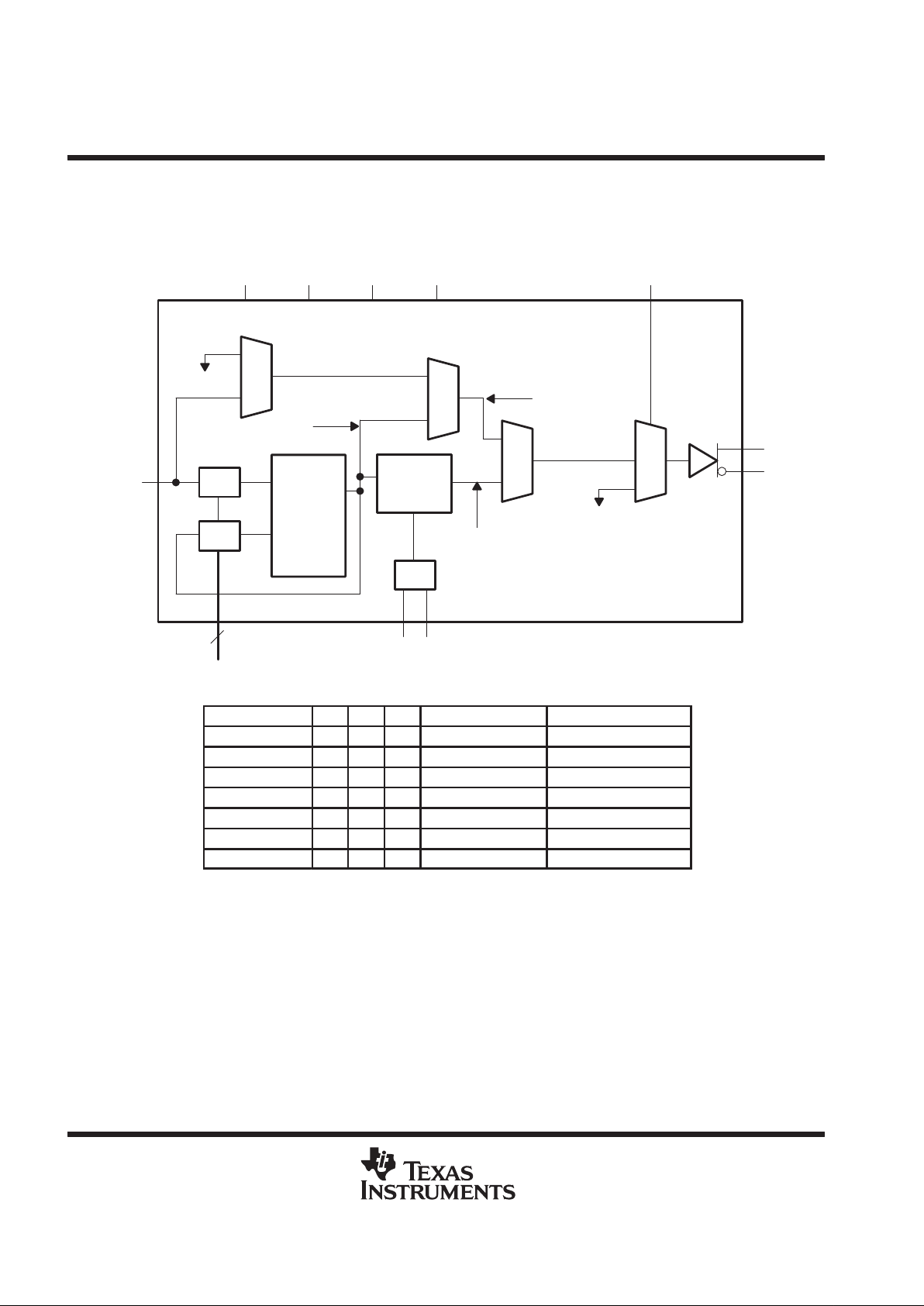
The DRCG provides clock multiplication and phase alignment for a Direct Rambus memory subsystem to
enable synchronous communication between the Rambus channel and ASIC clock domains. In a Direct
Rambus memory subsystem, a system clock source provides the REFCLK and PCLK clock references to the
DRCG and memory controller, respectively. The DRCG multiplies REFCLK and drives a high-speed BUSCLK
to RDRAMs and the memory controller. Gear ratio logic in the memory controller divides the PCLK and BUSCLK
frequencies by ratios M and N such that PCLK/M = SYNCLK/N, where SYNCLK = BUSCLK/4. The DRCG
detects the phase difference between PCLK/M and SYNCLK/N and adjusts the phase of BUSCLK such that
the skew between PCLK/M and SYNCLK/N is minimized. This allows data to be transferred across the
SYNCLK/PCLK boundary without incurring additional latency.
User control is provided by multiply and mode selection terminals. The multiply terminals provide selection of
one of four clock frequency multiply ratios, generating BUSCLK frequencies ranging from 267 MHz to 400 MHz
with clock references ranging from 33 MHz to 100 MHz. The CDCR81 meets Rambus Clock Generator,
Revision 1.0 specification up to 300 MHz. The mode select terminals can be used to select a bypass mode
where the frequency multiplied reference clock is directly output to the Rambus channel for systems where
synchronization between the Rambus clock and a system clock is not required. Test modes are provided to
bypass the PLL and output REFCLK on the Rambus channel and to place the outputs in a high-impedance state
for board testing.
Copyright 1999, Texas Instruments Incorporated
PRODUCTION DATA information is current as of publication date.
Products conform to specifications per the terms of Texas Instruments
standard warranty. Production processing does not necessarily include
testing of all parameters.
Please be aware that an important notice concerning availability, standard warranty, and use in critical applications of
Texas Instruments semiconductor products and disclaimers thereto appears at the end of this data sheet.
Direct Rambus and Rambus are trademarks of Rambus Inc.
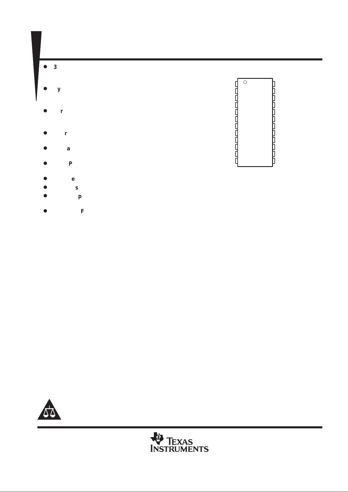
1
2
3
4
5
6
7
8
9
10
11
12
24
23
22
21
20
19
18
17
16
15
14
13
VDDIR
REFCLK
V
DD
P
GNDP
GNDI
PCLKM
SYNCLKN
GNDC
V
DD
C
V
DD
IPD
STOPB
PWRDNB
S0
S1
V
DD
O
GNDO
CLK
NC
CLKB
GNDO
V
DD
O
MULT0
MULT1
S2
DBQ PACKAGE
(TOP VIEW)
NC – No internal connection
Page 2
CDCR81
DIRECT RAMBUS CLOCK GENERATOR
SCAS606B – NOVEMBER 1998 – REVISED NOVEMBER 1999
2
POST OFFICE BOX 655303 • DALLAS, TEXAS 75265
description (continued)
The CDCR81 is characterized for operation over free-air temperatures of 0°C to 85°C.
functional block diagram
Bypass MUX
Test MUX
B
A
PLL
Phase
Aligner
PACLK
PLLCLK
ByPCLK
CLK
CLKB
REFCLK
φ
D
SYNCLKNPCLKM
MULT0
MULT1
2
PWRDWNB S0 S1 S2 STOPB
FUNCTION TABLE
†
MODE
S0 S1 S2 CLK CLKB
Normal 0 0 0 Phase aligned clock Phase aligned clock B
Bypass 1 0 0 PLLCLK PLLCLKB
Test 1 1 0 REFCLK REFCLKB
Output test (OE) 0 1 X Hi-Z Hi-Z
Reserved 0 0 1 — —
Reserved 1 0 1 — —
Reserved 1 1 1 Hi-Z Hi-Z
†
X = don’t care, Hi-Z = high impedance
Page 3
CDCR81
DIRECT RAMBUS CLOCK GENERATOR
SCAS606B – NOVEMBER 1998 – REVISED NOVEMBER 1999
3
POST OFFICE BOX 655303 • DALLAS, TEXAS 75265
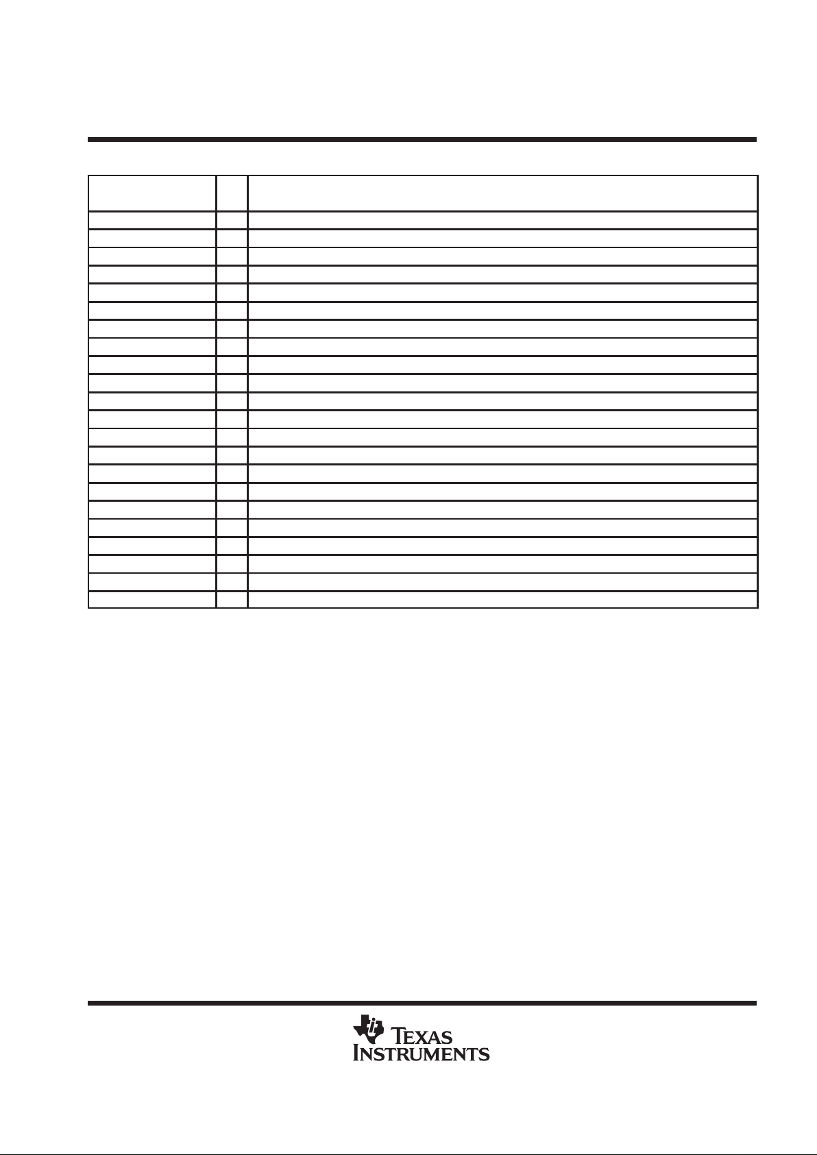
Terminal Functions
TERMINAL
NAME NO.
I/O
DESCRIPTION
CLK 20 O Output clock
CLKB 18 O Output clock (complement)
GNDC 8 GND for phase aligner
GNDI 5 GND for control inputs
GNDO 17, 21 GND for clock outputs
GNDP 4 GND for PLL
MULT0 15 I PLL multiplier select
MULT1 14 I PLL multiplier select
NC 19 Not used
PCLKM 6 I Phase detector input
PWRDNB 12 I Active low power down
REFCLK 2 I Reference clock
S0 24 I Mode control
S1 23 I Mode control
S2 13 I Mode control
STOPB 11 I Active low output disable
SYNCLKN 7 I Phase detector input
VDDC 9 VDD for phase aligner
VDDIPD 10 Reference voltage for phase detector inputs and STOPB
VDDIR 1 Reference voltage for REFCLK
VDDO 16, 22 VDD for clock outputs
VDDP 3 VDD for PLL
Page 4
CDCR81
DIRECT RAMBUS CLOCK GENERATOR
SCAS606B – NOVEMBER 1998 – REVISED NOVEMBER 1999
4
POST OFFICE BOX 655303 • DALLAS, TEXAS 75265
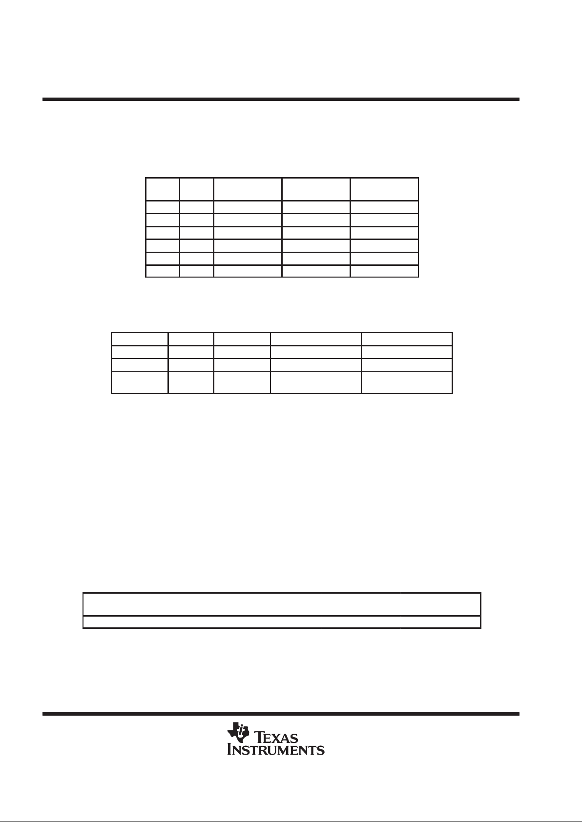
PLL divider selection
Table 1 lists the supported REFCLK and BUSCLK frequencies. Other REFCLK frequencies are permitted,
provided that (267 MHz < BUSCLK < 400 MHz) and (33 MHz < REFCLK < 100 MHz).
Table 1. REFCLK and BUSCLK Frequencies
MULT0 MULT1
REFCLK
(MHz)
MULTIPLY
RATIO
BUSCLK
(MHz)
0 0 67 4 267
0 1 50 6 300
0 1 67 6 400
1 1 33 8 267
1 1 50 8 400
1 0 100 8/3 267
clock output driver states
Table 2. Clock Output Driver States
STATE PWRDNB STOPB CLK CLKB
Powerdown 0 X GND GND
CLK stop 1 0 VX,
STOP
VX,
STOP
Normal 1 1
PACLK/PLLCLK/
REFCLK
†
PACLKB/PLLCLKB/
REFCLKB
†
Depending on the state of S0, S1, and S2.
absolute maximum ratings over operating free-air temperature (unless otherwise noted)
†
Supply voltage range, VDD (see Note 1) –0.5 V to 4 V. . . . . . . . . . . . . . . . . . . . . . . . . . . . . . . . . . . . . . . . . . . . . .
Output voltage range, VO, at any output terminal –0.5 V to V
DD
+ 0.5 V. . . . . . . . . . . . . . . . . . . . . . . . . . . . . . . .
Input voltage range,VI, at any input terminal –0.5 V to VDD + 0.5 V. . . . . . . . . . . . . . . . . . . . . . . . . . . . . . . . . . . .
ESD rating TBD. . . . . . . . . . . . . . . . . . . . . . . . . . . . . . . . . . . . . . . . . . . . . . . . . . . . . . . . . . . . . . . . . . . . . . . . . . . . . . . .
Continuous total power dissipation see Dissipation Rating Table. . . . . . . . . . . . . . . . . . . . . . . . . . . . . . . . . . . . . .
Operating free-air temperature range, T
A
0°C to 85°C. . . . . . . . . . . . . . . . . . . . . . . . . . . . . . . . . . . . . . . . . . . . . .
Storage temperature range, T
stg
–65°C to 150°C. . . . . . . . . . . . . . . . . . . . . . . . . . . . . . . . . . . . . . . . . . . . . . . . . . .
Lead temperature 1,6 mm (1/16 inch) from case for 10 seconds 260°C. . . . . . . . . . . . . . . . . . . . . . . . . . . . . . .
†
Stresses beyond those listed under “absolute maximum ratings” may cause permanent damage to the device. These are stress ratings only, and
functional operation of the device at these or any other conditions beyond those indicated under “recommended operating conditions” is not
implied. Exposure to absolute-maximum-rated conditions for extended periods may affect device reliability.
NOTE 1: All voltage values are with respect to the GND terminals.
DISSIPATION RATING TABLE
PACKAGE
TA ≤ 25°C
POWER RATING
DERATING FACTOR
ABOVE TA = 25°C
‡
TA = 70°C
POWER RATING
TA = 85°C
POWER RATING
DBQ 1400 mW 11 mW/°C 905 mW 740 mW
‡
This is the inverse of the junction-to-ambient thermal resistance when board-mounted and with no air flow.
Page 5
CDCR81
DIRECT RAMBUS CLOCK GENERATOR
SCAS606B – NOVEMBER 1998 – REVISED NOVEMBER 1999
5
POST OFFICE BOX 655303 • DALLAS, TEXAS 75265
recommended operating conditions
MIN NOM MAX UNIT
Supply voltage, V
DD
3.135 3.3 3.465 V
High-level input voltage, VIH (CMOS) 0.7×V
DD
V
Low-level input voltage, VIL (CMOS) 0.3×V
DD
V
Initial phase error at phase detector inputs
(required range for phase aligner)
–0.5×t
c(PD)
0.5×t
c(PD)
REFCLK low-level input voltage, V
IL
0.3×VDDIR V
REFCLK high-level input voltage, V
IH
0.7×VDDIR V
Input signal low voltage, VIL (STOPB) 0.3×VDDIPD V
Input signal high voltage, VIH (STOPB) 0.7×VDDIPD V
Input reference voltage for (REFCLK) (VDDIR) 1.235 3.465 V
Input reference voltage for (PCLKM and SYSCLKN) (VDDIPD) 1.235 3.465 V
High-level output current, I
OH
–16 mA
Low-level output current, I
OL
16 mA
Operating free-air temperature, T
A
0 85 °C
timing requirements
MIN MAX UNIT
Input cycle time, t
c(in)
10 40 ns
Input cycle-to-cycle jitter 250 ps
Input duty cycle over 10,000 cycles 40% 60%
Input frequency modulation, f
mod
30 33 kHz
Modulation index, non-linear maximum 0.5% 0.6%
Phase detector input cycle time (PCLKM and SYNCLKN) 30 100 ns
Input slew rate, SR 1 4 V/ns
Input duty cycle (PCLKM and SYNCLKN) 25% 75%
Page 6
CDCR81
DIRECT RAMBUS CLOCK GENERATOR
SCAS606B – NOVEMBER 1998 – REVISED NOVEMBER 1999
6
POST OFFICE BOX 655303 • DALLAS, TEXAS 75265
electrical characteristics over recommended operating free-air temperature range (unless
otherwise noted)
PARAMETER TEST CONDITIONS
†
MIN TYP‡MAX UNIT
V
O(STOP)
Output voltage during CLK Stop (StopB=0) See Figure 1 1.1 2
V
O(X)
Output crossing-point voltage See Figures 1 and 6 1.3 1.8 V
V
O
Output voltage swing See Figure 1 0.4 0.6 V
V
IK
Input clamp voltage VDD = 3.135 V , II = –18 mA –1.2 V
See Figure 1 2
V
OH
High-level output voltage
VDD = min to max,
IOH = –1 mA
VDD–
0.1 V
V
VDD = 3.135 V , IOH = –16 mA 2.4
See Figure 1 1
V
OL
Low-level output voltage
VDD = min to max,
IOL = 1 mA 0.1
V
VDD = 3.135 V , IOL = 16 mA 0.5
VDD = 3.135 V , VO = 1 V –32 –52
I
OH
High-level output current
VDD = 3.3 V,
VO = 1.65 V –51
mA
VDD = 3.465 V , VO = 3.135 V –14.5 –21
VDD = 3.135 V , VO = 1.95 V 43 61.5
I
OL
Low-level output current
VDD = 3.3 V,
VO = 1.65 V 65
mA
VDD = 3.465 V , VO = 0.4 V 25.5 36
I
OZ
High-impedance-state output current S0 = 0, S1 = 1 ±10 µA
I
OZ(STOP)
High-impedance-state output current
during CLK stop
Stop= 0, VO = GND or V
DD
±100 µA
I
OZ(PD)
High-impedance-state output current in
powerdown state
PWDNB= 0,
VO = GND or V
DD
–10 100 µA
High-level input
REFCLK, PCLKM,
SYNCLKN, STOPB
VDD = 3.465 V , VI = V
DD
10
I
IH
g
current
PWRDNB, S0, S1,
S2, MULT0, MULT1
VDD = 3.465 V , VI = V
DD
10
µ
A
Low-level input
REFCLK, PCLKM,
SYNCLKN, STOPB
VDD = 3.465 V , VI = 0 –10
I
IL
current
PWRDNB, S0, S1,
S2, MULT0, MULT1
VDD = 3.465 V , VI = 0 –10
µ
A
p
p
High state RI at IO –14.5 mA to –16.5 mA 15 26 40
ZOOutput impedance
Low state RI at IO 14.5 mA to 16.5 mA 11 17 35
Ω
PWRDNB = 0 50 µA
Reference current
VDDIR, VDDIPD
V
DD
= 3.
465 V
,
PWRDNB = 1 0.5 mA
C
I
Input capacitance VI = VDD or GND 1.8 pF
C
O
Output capacitance VO = VDD or GND 3.1 pF
I
DD(PD)
Supply current in powerdown state
REFCLK = 0 MHz to 100 MHz,
PWDNB = 0, STOPB = 1
200 µA
I
DD(CLKSTOP)
Supply current in CLK stop state BUSCLK configured for 400 MHz 30 mA
I
DD(NORMAL)
Supply current in normal state BUSCLK = 400 MHz 70 mA
†
VDD refers to any of the following; VDD, VDDIPD, VDDIR, VDDO, VDDC, and VDDP
‡
All typical values are at VDD = 3.3 V, TA = 25°C.
Page 7
CDCR81
DIRECT RAMBUS CLOCK GENERATOR
SCAS606B – NOVEMBER 1998 – REVISED NOVEMBER 1999
7
POST OFFICE BOX 655303 • DALLAS, TEXAS 75265
switching characteristics over recommended operating free-air temperature range (unless
otherwise noted)
PARAMETER TEST CONDITIONS MIN TYP†MAX UNIT
t
c(out) Clock output cycle time
2.5 3.75 ns
Total cycle jitter over 1, 2
,
Stopped phase
alignment
267 MHz –
400 MHz
See Figure 3 60 ps
t
(jitter)
Total cycle jitter over 1, 2,
3, 4, 5, or 6 clock cycles
Infinite phase
267 MHz
80
p
alignment
300 MHz
See Figure 3
70
ps
t
(phase)
Phase detector phase error for distributed loop Static phase error –50 50 ps
t
(phase, SSC)
PLL output phase error when tracking SSC Dynamic phase error –100 100 ps
t
(DC)
Output duty cycle over 10,000 cycles See Figure 4 45% 55%
Stopped phase
alignment
267 MHz –
400 MHz
See Figure 5 50 ps
t
Output cycle-to-cycle
267 MHz 70
(DC,err)
duty cycle error
Infinite phase
300 MHz
See Figure 5
80
ps
alignment
400 MHz 90
tr, t
f
Output rise and fall times (measured at 20%-80% of
output voltage)
See Figure 7 200 450 ps
∆t
Difference between rise and fall times on a single device
(20%–80%) |tf – tr|
See Figure 7 100 ps
†
All typical values are at VDD = 3.3 V, TA = 25°C.
state transition latency specifications
PARAMETER FROM TO
TEST
CONDITIONS
MIN TYP†MAX UNIT
Delay time, PWRDNB↑ to CLK/CLKB output
settled (excluding t
(DISTLOCK)
)
Power-
See Figure 8 3
t
(powerup)
Delay time, PWRDNB↑ to internal PLL and
clock are on and settled
down
Normal3ms
Delay time, powerup to CLK/CLKB output
settled
See Figure 8 3
t
(VDDpowerup)
Delay time, powerup to internal PLL and clock
are on and settled
VDDNormal3ms
t
(MULT)
MULT0 and MULT1 change to CLK/CLKB
output resettled (excluding t
(DISTLOCK)
)
Normal Normal See Figure 9 1 ms
t
(CLKON)
STOPB↑ to CLK/CLKB glitch-free clock edges
CLK
Stop
Normal See Figure 10 10 ns
t
(CLKSETL)
STOPB↑ to CLK/CLKB output settled to within
50 ps of the phase before STOPB was disabled
CLK
Stop
Normal See Figure 10 20 cycles
t
(CLKOFF)
STOPB↑ to CLK/CLKB output disabled Normal
CLK
Stop
See Figure 10 5 ns
t
(powerdown)
Delay time, PWRDNB↓ to the device in powerdown mode
STOPB
Powerdown
1 ms
t
(STOP)
Maximum time in CLKSTOP (STOPB = 0)
before re-entering normal mode (STOPB = 1)
STOPB Normal 100 µs
Page 8
CDCR81
DIRECT RAMBUS CLOCK GENERATOR
SCAS606B – NOVEMBER 1998 – REVISED NOVEMBER 1999
8
POST OFFICE BOX 655303 • DALLAS, TEXAS 75265
state transition latency specifications (continued)
PARAMETER FROM TO
TEST
CONDITIONS
MIN TYP†MAX UNIT
t
(ON)
Minimum time in normal mode (STOPB = 1)
before re-entering CLKSTOP (STOPB = 0)
Normal
CLK
stop
100 ms
t
(DISTLOCK)
Time from when CLK/CLKB output is settled to
when the phase error between SYNCLKN and
PCLKM falls within t
(ERR-PD)
Un-
locked
Locked 5 ms
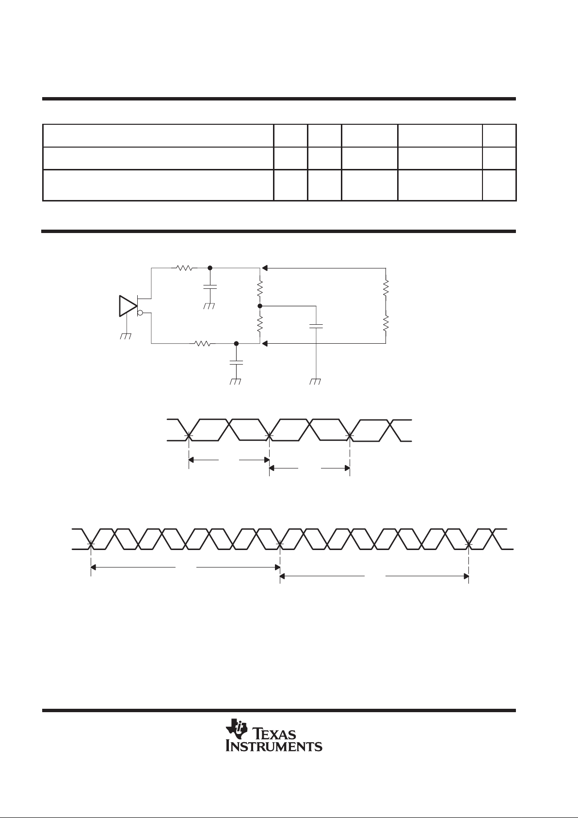
PARAMETER MEASUREMENT INFORMATION
39 Ω, ±5%
68 Ω, ±5%
68 Ω, ±5%
10 pF
100 pF
39 Ω, ±5%
10 pF
RT = 28 Ω
RT = 28 Ω
Figure 1. Test Load and Voltage Definitions (V
O(STOP)
, V
O(X)
, VO, VOH, VOL)
CLK
CLKB
t
c1
t
c2
Cycle-to-cycle jitter = | tc1 – tc2| over 10000 consecutive cycles
Figure 2. Cycle-to-Cycle Jitter
CLK
CLKB
t
c3
Cycle-to-cycle jitter = | tc3 – tc4| over 10000 consecutive cycles
t
c4
Figure 3. Short Term Cycle-to-Cycle Jitter over 4 Cycles
Page 9

CDCR81
DIRECT RAMBUS CLOCK GENERATOR
SCAS606B – NOVEMBER 1998 – REVISED NOVEMBER 1999
9
POST OFFICE BOX 655303 • DALLAS, TEXAS 75265
PARAMETER MEASUREMENT INFORMATION
CLK
CLKB
t
pd1
t
c5
Duty cycle = (t
Pd1/tc5
)
Figure 4. Output Duty Cycle
CLK
CLKB
t
pd2
t
c6
Duty cycle error = t
pd2
– t
pd3
t
pd3
t
c7
Figure 5. Duty Cycle Error (Cycle-to-Cycle)
CLK
CLKB
V
O(X)+
V
O(X), nom
V
O(X)–
Figure 6. Crossing-Point Voltage
80%
t
f
t
r
20%
V
OL
V
OH
Figure 7. Voltage Waveforms
ООООООО
PWRDNB
CLK/CLKB
t
powerdown
t
powerup
Figure 8. PWRDNB Transition Timings
Page 10

CDCR81
DIRECT RAMBUS CLOCK GENERATOR
SCAS606B – NOVEMBER 1998 – REVISED NOVEMBER 1999
10
POST OFFICE BOX 655303 • DALLAS, TEXAS 75265
PARAMETER MEASUREMENT INFORMATION
MULT0 and/or
MULT1
CLK/CLKB
t
MULT
Figure 9. MULT Transition Timings
STOPB
t
CLKOFF
(see Note A)
t
ON
t
STOP
t
CLKSETL
t
CLKON
(see Note A)
Clock output settled
within 50 ps of the
phase before disabled
Clock enabled
and glitch free
Output clock
not specified
glitches ok
CLK/CLKB
NOTE A: V
ref
= VO ±200 mV
Figure 10. STOPB Transition Timings
Page 11
CDCR81
DIRECT RAMBUS CLOCK GENERATOR
SCAS606B – NOVEMBER 1998 – REVISED NOVEMBER 1999
11
POST OFFICE BOX 655303 • DALLAS, TEXAS 75265
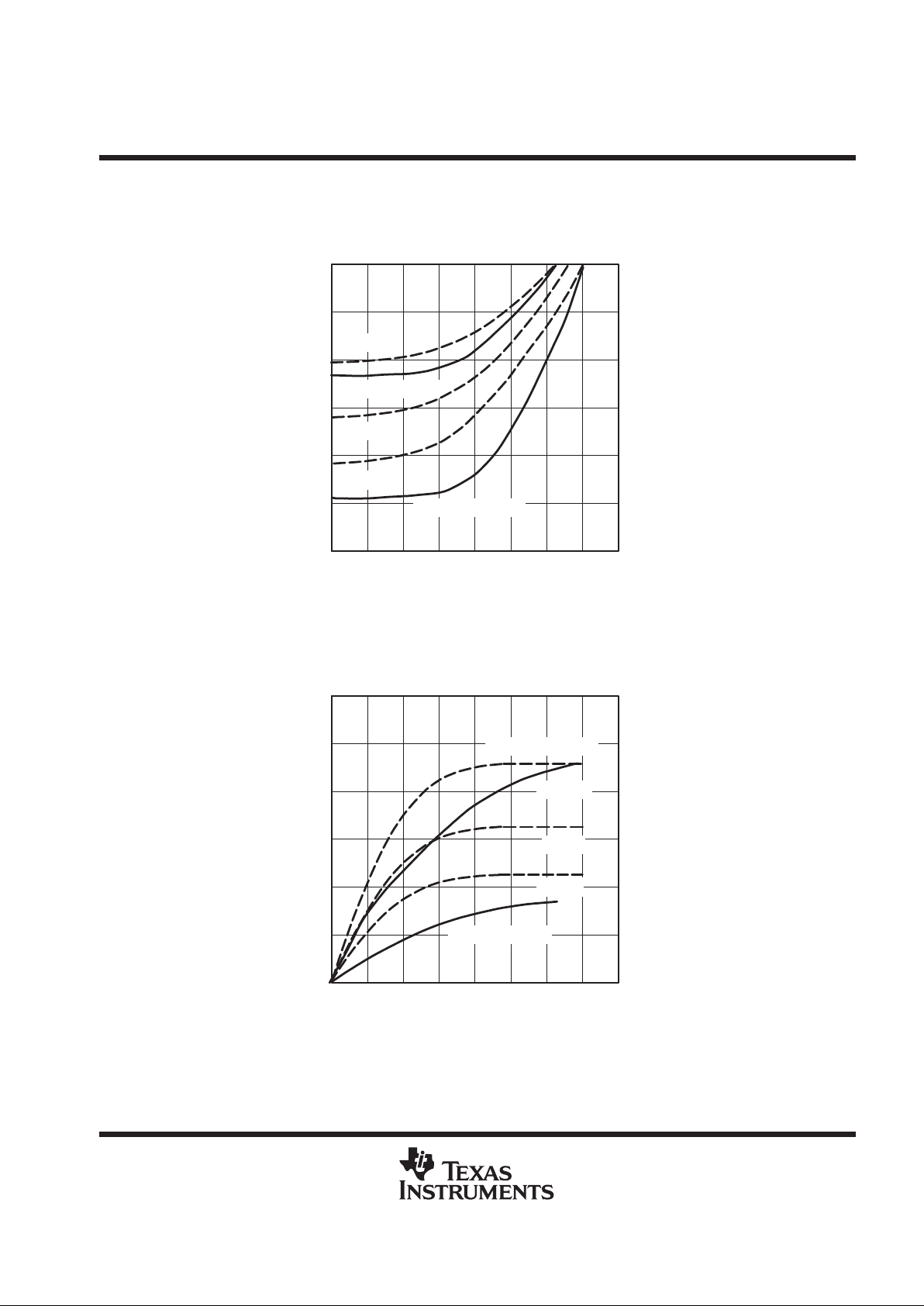
PARAMETER MEASUREMENT INFORMATION
VOH – High-Level Output Voltage – V
HIGH-LEVEL OUTPUT CURRENT
vs
HIGH-LEVEL OUTPUT VOLTAGE
0
–0.04
–0.08
–0.12
0.5 1.5
–0.02
–0.06
–0.1
120
2.5 3 3.5 4
I
OH
– High-Level Output Current – A
Strong
Weak
Nom
Rambus (min)
Rambus (max)
Figure 11. Pullup IBIS I/V Chart
VOL – Low-Level Output Voltage – V
LOW-LEVEL OUTPUT CURRENT
vs
LOW-LEVEL OUTPUT VOLTAGE
0.12
0.08
0.04
0
0.5 1.5
0.1
0.06
0.02
120
2.5 3 3.5 4
I
OL
– Low-Level Output Current – A
Strong
Weak
Nom
Rambus (min)
Rambus (max)
Figure 12. Pulldown IBIS I/V Chart
Page 12

CDCR81
DIRECT RAMBUS CLOCK GENERATOR
SCAS606B – NOVEMBER 1998 – REVISED NOVEMBER 1999
12
POST OFFICE BOX 655303 • DALLAS, TEXAS 75265
MECHANICAL DATA
DBQ (R-PDSO-G**) PLASTIC SMALL-OUTLINE PACKAGE
Gage Plane
0.008 (0,20) NOM
0.010 (0,25)
0.016 (0,40)
0.035 (0,89)
2420
Seating Plane
(8,74)
(8,56)
0.3370.337
(8,56)
(8,74)
0.344 0.344
4073301/C 02/97
13
0.150 (3,81)
0.157 (3,99)
0.012 (0,30)
0.008 (0,20)
12
A
24–PIN SHOWN
1
24
16
DIM
PINS **
A MIN
A MAX
0.004 (0,10)
0.010 (0,25)
0.069 (1,75) MAX
0.244 (6,20)
0.228 (5,80)
0.197
(5,00)
(4,78)
0.188
0.004 (0,10)
M
0.005 (0,13)
0.025 (0,64)
0°–8°
NOTES: A. All linear dimensions are in inches (millimeters).
B. This drawing is subject to change without notice.
C. Body dimensions do not include mold flash or protrusion not to exceed 0.006 (0,15).
D. Falls within JEDEC MO-137
Page 13

IMPORTANT NOTICE
T exas Instruments and its subsidiaries (TI) reserve the right to make changes to their products or to discontinue
any product or service without notice, and advise customers to obtain the latest version of relevant information
to verify, before placing orders, that information being relied on is current and complete. All products are sold
subject to the terms and conditions of sale supplied at the time of order acknowledgement, including those
pertaining to warranty, patent infringement, and limitation of liability.
TI warrants performance of its semiconductor products to the specifications applicable at the time of sale in
accordance with TI’s standard warranty. Testing and other quality control techniques are utilized to the extent
TI deems necessary to support this warranty. Specific testing of all parameters of each device is not necessarily
performed, except those mandated by government requirements.
CERT AIN APPLICATIONS USING SEMICONDUCTOR PRODUCTS MAY INVOLVE POTENTIAL RISKS OF
DEATH, PERSONAL INJURY, OR SEVERE PROPERTY OR ENVIRONMENTAL DAMAGE (“CRITICAL
APPLICATIONS”). TI SEMICONDUCTOR PRODUCTS ARE NOT DESIGNED, AUTHORIZED, OR
WARRANTED TO BE SUITABLE FOR USE IN LIFE-SUPPORT DEVICES OR SYSTEMS OR OTHER
CRITICAL APPLICATIONS. INCLUSION OF TI PRODUCTS IN SUCH APPLICA TIONS IS UNDERSTOOD T O
BE FULLY AT THE CUSTOMER’S RISK.
In order to minimize risks associated with the customer’s applications, adequate design and operating
safeguards must be provided by the customer to minimize inherent or procedural hazards.
TI assumes no liability for applications assistance or customer product design. TI does not warrant or represent
that any license, either express or implied, is granted under any patent right, copyright, mask work right, or other
intellectual property right of TI covering or relating to any combination, machine, or process in which such
semiconductor products or services might be or are used. TI’s publication of information regarding any third
party’s products or services does not constitute TI’s approval, warranty or endorsement thereof.
Copyright 1999, Texas Instruments Incorporated
 Loading...