

Page 1
查询CDCR61A供应商
CDCR61A
DIRECT RAMBUS CLOCK GENERATOR – LITE
SCAS626 – FEBRUARY 2000
D
400-MHz Differential Clock Source for
Direct Rambus Memory Systems for an
800-MHz Data Transfer Rate
D
Operates From Two (3.3-V and 1.80-V)
Power Supplies With 180 mW (Typ) at 400
MHz Total
D
Packaged in a Thin Shrink Small-Outline
Package (PW)
D
External Crystal Required for Input
V
DDP
GNDP
XOUT
XIN
V
DDL
LCLK
GNDL
S1
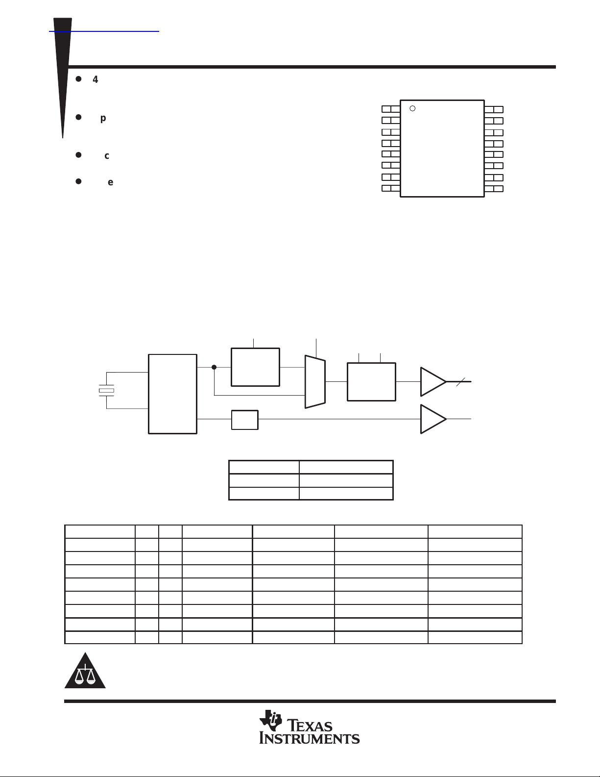
PW PACKAGE
(TOP VIEW)
1
2
3
4
5
6
7
8
16
15
14
13
12
11
10
9
description
The Direct Rambus clock generator – lite (DRCG-Lite) is an independent crystal clock generator. It performs
clock multiplication using PLL, sourced by an internal crystal oscillator. It provides one dif ferential, high-speed
Rambus channel compatible output pair. Also, one single-ended output is available to deliver 1/2 of the crystal
frequency. The Rambus channel operates at up to 400 MHz with an option to select 300 MHz as well. The
desired crystal is a 18.75-MHz crystal in a series resonance fundamental application.
The CDCR61A is characterized for operation over free-air temperatures of 0°C to 85°C.
functional block diagram
XTAL
XIN
OSC
S0
PLL
V
DDP
S1 S2
DIV
2
BUSCLK
S0
V
DD
GND
CLK
CLKB
GND
V
DD
S2
XOUT
V
DDP
ON 0 0 Normal CLK CLKB XIN divided by 2
ON 1 1 Normal CLK CLKB XIN divided by 2
ON 0 1 Test Divided by 2 Divided by 2 XIN divided by 2
ON 1 0 Test Divided by 4 Divided by 4 XIN divided by 2
0 V 0 0 Test XIN XIN (invert) XIN divided by 2
0 V 1 1 Test XIN XIN (invert) XIN divided by 2
0 V 0 1 Test XIN divided by 2 XIN (invert) divided by 2 XIN divided by 2
0 V 1 0 Test XIN divided by 4 XIN (invert) divided by 4 XIN divided by 2
Direct Rambus and Rambus are trademarks of Rambus Inc.
PRODUCTION DATA information is current as of publication date.
Products conform to specifications per the terms of Texas Instruments
standard warranty. Production processing does not necessarily include
testing of all parameters.
S1 S2 MODE CLK CLKB LCLK
Please be aware that an important notice concerning availability, standard warranty, and use in critical applications of
Texas Instruments semiconductor products and disclaimers thereto appears at the end of this data sheet.
/2
BUSCLK FREQUENCY SETTINGS
S0
0 16
1 or Open 64/3
FUNCTION TABLE
M (PLL MULTIPLIER)
Copyright 2000, Texas Instruments Incorporated
LCLK
POST OFFICE BOX 655303 • DALLAS, TEXAS 75265
1
Page 2
CDCR61A
I/O
DESCRIPTION
DIRECT RAMBUS CLOCK GENERATOR – LITE
SCAS626 – FEBRUARY 2000
Terminal Functions
TERMINAL
NAME NO.
CLK 13 O Output clock, connect to Rambus channel
CLKB 12 O Output clock (complement), connect to Rambus channel
GNDP, GNDL,
GND
LCLK 6 O LVCMOS output, 1/2 of crystal frequency
S0, S1, S2 16, 8, 9 I LVTTL level logic select terminal for function selection
V
DD
V
DDP
V
DDL
XIN 4 I Reference crystal input
XOUT 3 O Reference crystal feedback
2, 7,
11, 14
10, 15 Power supply, 3.3 V
1 Power supply for PLL, 3.3 V (0 V for Test mode)
5 Power supply for LCLK, 1.8 V
Ground
absolute maximum ratings over operating free-air temperature (unless otherwise noted)
Supply voltage range, VDD or V
Supply voltage range, V
Input voltage range,V
(see Note 1) –0.5 V to 4 V. . . . . . . . . . . . . . . . . . . . . . . . . . . . . . . . . . . . . . . . . . . . .
DDL
, at any input terminal –0.5 V to VDD + 0.5 V. . . . . . . . . . . . . . . . . . . . . . . . . . . . . . . . . . . .
I
Output voltage range, VO, at any output terminal (CLK, CLKB) –0.5 V to V
Output voltage range, VO, at any output terminal (LCLK) –0.5 V to V
(see Note 1) –0.5 V to 4 V. . . . . . . . . . . . . . . . . . . . . . . . . . . . . . . . . . . . . .
DDP
†
DD
DDL
+ 0.5 V. . . . . . . . . . . . . . . . . . . .
+ 0.5 V. . . . . . . . . . . . . . . . . . . . . . . .
ESD rating (MIL-STD 883C, Method 3015) > 2 kV, Machine Model >200 V. . . . . . . . . . . . . . . . . . . . . . . . . . . . .
Continuous total power dissipation see Dissipation Rating Table. . . . . . . . . . . . . . . . . . . . . . . . . . . . . . . . . . . . . .
Operating free-air temperature range, T
Storage temperature range, T
–65°C to 150°C. . . . . . . . . . . . . . . . . . . . . . . . . . . . . . . . . . . . . . . . . . . . . . . . . . .
stg
0°C to 85°C. . . . . . . . . . . . . . . . . . . . . . . . . . . . . . . . . . . . . . . . . . . . . .
A
Lead temperature 1,6 mm (1/16 inch) from case for 10 seconds 260°C. . . . . . . . . . . . . . . . . . . . . . . . . . . . . . .
†
Stresses beyond those listed under “absolute maximum ratings” may cause permanent damage to the device. These are stress ratings only, and
functional operation of the device at these or any other conditions beyond those indicated under “recommended operating conditions” is not
implied. Exposure to absolute-maximum-rated conditions for extended periods may affect device reliability.
NOTE 1: All voltage values are with respect to the GND terminals.
DISSIPATION RATING TABLE
PACKAGE
PW 1400 mW 11 mW/°C 740 mW
‡
This is the inverse of the junction-to-ambient thermal resistance when board-mounted and with
no air flow.
TA ≤ 25°C
POWER RATING
DERATING FACTOR
ABOVE TA = 25°C
‡
POWER RATING
TA = 85°C
2
POST OFFICE BOX 655303 • DALLAS, TEXAS 75265
Page 3
Low-level input voltage, V
V
High-level input voltage, V
V
Internal pullup resistance
kΩ
Low-level output current, I
mA
High-level output current, I
mA
I
(CMOS), C
†
pF
CDCR61A
DIRECT RAMBUS CLOCK GENERATOR – LITE
SCAS626 – FEBRUARY 2000
recommended operating conditions
MIN NOM MAX UNIT
Supply voltage, V
LCLK supply voltage, V
p
Input frequency at crystal input 14.0625 18.75 MHz
nput capacitance
Operating free-air temperature, T
†
Capacitance measured at f = 1 MHz, dc bias = 0.9 V, and VAC < 100 mV
DD
DDL
p
p
p
p
p
IL
IH
OL
OH
I
A
S0 0.35×V
S1, S2 0.35×V
S0 0.65×V
S1, S2 0.65×V
S0 10 55 100
S1, S2 90 145 250
CLK, CLKB 16
LCLK 10
CLK, CLKB –16
LCLK –10
S0, S1, S2 2.5
XIN, XOUT 20
3 3.3 3.6 V
1.7 1.8 2.1 V
DD
DD
DD
DD
0 85 °C
p
timing requirements
MIN MAX UNIT
Clock cycle time, t
Input slew rate, SR 0.5 4 V/ns
State transition latency (V
(cycle)
or S0 to CLKs – normal mode), t
DDX
(STL)
2.5 3.7 ns
3 ms
crystal specifications
MIN MAX UNIT
Frequency 14.0625 18.75 MHz
Frequency tolerance (at 25°C ±3°C) –15 15 ppm
Equivalent resistance (CL = 10 pF) 100 Ω
Temperature drift (–10°C to 75°C) 10 ppm
Drive level 0.01 1500 µW
Motional inductance 20.7 25.3 mH
Insulation resistance 500 MΩ
Spurious attenuation ratio (at frequency ±500 kHz) 3 dB
Overtone spurious 8 dB
POST OFFICE BOX 655303 • DALLAS, TEXAS 75265
3
Page 4

CDCR61A
A
A
VOHHigh-level output voltage
V
VOLLow-level output voltage
V
IOHHigh-level output current
mA
IOLLow-level output current
mA
COOutput capacitance
pF
DIRECT RAMBUS CLOCK GENERATOR – LITE
SCAS626 – FEBRUARY 2000
electrical characteristics over recommended operating free-air temperature range (unless
otherwise noted)
PARAMETER TEST CONDITIONS
V
O(X)
V
O(PP)
V
IK
R
I
I
IH
I
IL
r
OH
r
OL
†
VDD refers to any of the following; VDD, V
‡
All typical values are at VDD = 3.3 V, V
§
rO = ∆VO/∆IO. This is defined at the output terminals, not at the measurement point of Figure 1.
Differential crossing-point output voltage See Figures 1 and 7 1.25 1.85 V
Peak-to-peak output voltage swing,
single ended
Input clamp voltage VDD = 3 V, II = –18 mA –1.2 V
Input resistance XIN, XOUT VDD = 3.3 V, VI = V
XOUT VDD = 3.3 V, VO = 2 V 27 mA
High-level input current
Low-level input current
p
p
p
p
High-level dynamic output resistance
Low-level dynamic output resistance
p
p
DDL
S0
S1, S2 VDD = 3.6 V, VI = V
XOUT VDD = 3.3 V, VO = 0 V –5.7 mA
S0
S1, S2 VDD = 3.6 V, VI = 0 V –10 –50
CLK, CLKB
LCLK V
CLK, CLKB
LCLK V
CLK, CLKB
LCLK
CLK, CLKB
LCLK
CLK, CLKB 3
LCLK 3
, and V
DDL
= 1.8 V, TA = 25°C.
VOH – VOL, See Figure 1 0.4 0.7 V
VDD = 3.6 V, VI = V
VDD = 3.6 V, VI = 0 V –30 –100
See Figure 1 2.1
VDD = min to max, IOH = –1 mA
VDD = 3 V, IOH = –16 mA 2.2
= min to max, IOH = – 10 mA
DDL
See Figure 1 1
VDD = min to max, IOL = 1 mA 0.1
VDD = 3 V, IOL = 16 mA 0.5
= min to max, IOL = 10 mA 0 0.45
DDL
VDD = 3.135 V, VO = 1 V –32 –52
VDD = 3.3 V, VO = 1.65 V –51
VDD = 3.465 V, VO = 3.135 V –14.5 –21
V
= 1.7 V, VO = 0.5 V –11 –26
DDL
V
= 1.8 V, VO = 0.9 V –28
DDL
V
= 2.1 V, VO = 1.6 V –24.5 –35
DDL
VDD = 3.135 V, VO = 1.95 V 43 61.5
VDD = 3.3 V, VO = 1.65 V 65
VDD = 3.465 V, VO = 0.4 V 25.5 36
V
= 1.7 V, VO = 1.2 V 11 27
DDL
V
= 1.8 V, VO = 0.9 V 30
DDL
V
= 2.1 V, VO = 0.5 V 28 38
DDL
§
∆IO – 14.5 mA to ∆IO – 16.5 mA 12 25 40 Ω
§
∆IO + 14.5 mA to ∆IO + 16.5 mA 12 17 40 Ω
DDP
†
O
DD
DD
MIN TYP‡MAX UNIT
>50 kΩ
10
10
VDD–
0.1 V
V
–
DDL
0.45 V
V
DDL
µ
µ
p
4
POST OFFICE BOX 655303 • DALLAS, TEXAS 75265
Page 5

I
Supply current in normal state
t
j ,,,,,
See Figure 3
ps
tjLLong-term jitter
See Figure 4
ps
t
Output cycle-to-cycle duty cycle error
See Figure 6
ps
PLL loop bandwidth
dB
CDCR61A
DIRECT RAMBUS CLOCK GENERATOR – LITE
SCAS626 – FEBRUARY 2000
electrical characteristics over recommended operating free-air temperature range (unless
otherwise noted) (continued)
PARAMETER TEST CONDITIONS
I
DD
I
DDL
DD(NORMAL)
I
DDL(NORMAL)
†
VDD refers to any of the following; VDD, V
‡
All typical values are at VDD = 3.3 V, V
Static supply current Outputs high or low (V
Static supply current (LVCMOS) Outputs high or low (V
pp
Supply current in normal state
(LVCMOS)
DDL
= 1.8 V, TA = 25°C.
DDL
, and V
300 MHz 39 mA
400 MHz 50 mA
400 MHz 8 mA
DDP
switching characteristics over recommended operating free-air temperature range (unless
otherwise noted)
PARAMETER TEST CONDITIONS MIN TYP
t
(cycle)
cj
t
DC
DC,ERR
tr, t
f
∆t
t
c(LCLK)
t
(cj)
t
(cj10)
t
DC
tr, t
f
†
All typical values are at VDD = 3.3 V, TA = 25°C.
‡
Output short-term jitter specification is peak-to-peak (see Figure 9).
§
LCLK cycle jitter and 10-cycle jitter are defined as the difference between the measured period and the nominal period.
¶
LCLK 10-cycle jitter specification is based on the measured value of LCLK cycle jitter.
#
VDD= 3.3 V
Clock cycle time (CLK, CLKB) 2.5 3.7 ns
Total jitter over 1, 2, 3, 4, 5, or 6
clock cycles
Output duty cycle over 10,000 cycles See Figure 5 45% 55%
Output rise and fall times (measured
at 20%-80% of output voltage)
Difference between rise and fall times on a single
device (20%–80%) |tf – tr|
Clock cycle time (LCLK) 106.6 142.2 ns
LCLK cycle jitter
LCLK 10-cycle jitter
Output duty cycle LCLK 40% 60%
Output rise and fall times (measured
at 20%-80% of output voltage)
‡
p
#
#
§
§¶
p
300 MHz
400 MHz
300 MHz
400 MHz
300 MHz
400 MHz
CLK, CLKB See Figure 9, 160 400 ps
See Figure 9, 100 ps
See Figure 11 –0.2 0.2 ns
See Figure 11 –1.3 t
LCLK See Figure 9 1 ns
f
= 50 kHz –3
mod
f
= 8 MHz –20
mod
†
= 0 V) 6.5 mA
DDP
= 0 V) 50 µA
DDP
MIN TYP‡MAX UNIT
†
MAX UNIT
(cj)
1.3 t
140
100
400
300
70
55
(cj)
p
p
p
ns
POST OFFICE BOX 655303 • DALLAS, TEXAS 75265
5
Page 6

CDCR61A
DIRECT RAMBUS CLOCK GENERATOR – LITE
SCAS626 – FEBRUARY 2000
PARAMETER MEASUREMENT INFORMATION
68 Ω, ±5%
CLK
3 pF
See Note A
68 Ω, ±5%
NOTE A: These capacitors represent parasitic capacitance. No discrete capacitors are used on the test
board during device characterization.
Figure 1. Test Load and Voltage Definitions (V
CLK
CLKB
Cycle-to-cycle jitter = | tc1 – tc2| over 10000 consecutive cycles
39 Ω, ±5%
39 Ω, ±5%
3 pF
See Note A
t
c1
100 pF
O(STOP)
t
c2
RT = 28 Ω
RT = 28 Ω
, V
O(X)
, VO, VOH, VOL)
Figure 2. Cycle-to-Cycle Jitter
(CLK)
Measurement
Node
(CLKB)
CLKB
t
c(i)
t
= nominal expected time
c(i)
Cycle-to-cycle jitter = | t
c(i)
– t
| over 10000 consecutive cycles
c(i+1)
t
c(i+1)
Figure 3. Short-Term Cycle-to-Cycle Jitter over 2, 3, 4, or 6 Cycles
CLK
CLKB
t
(cycle)
tjL = | t
(cycle), max
– t
(cycle), min
| over 10000 consecutive cycles
Figure 4. Long-Term Jitter
6
POST OFFICE BOX 655303 • DALLAS, TEXAS 75265
Page 7

CDCR61A
DIRECT RAMBUS CLOCK GENERATOR – LITE
SCAS626 – FEBRUARY 2000
PARAMETER MEASUREMENT INFORMATION
CLK
CLK
CLKB
Duty cycle error (t
CLK
CLKB
CLKB
Duty cycle (tDC) = (t
t
pW+/t(cycle)
(cycle)
)
t
pW+
Figure 5. Output Duty Cycle
t
pW+(i)
DC,ERR
) = t
t
(cycle)
pW+(i)
– t
pW+(i+1)
t
(cycle)
Figure 6. Duty Cycle Error (Cycle-to-Cycle)
Figure 7. Crossing-Point Voltage
t
pW+(i+1)
V
O(X)+
V
O(X), nom
V
O(X)–
1.8 V
LCLK
10 pF
120 Ω
120 Ω
20%
t
r
80%
t
f
V
OH
V
OL
Figure 8. LCLK Test Load Circuit and Voltage Waveform for CLK/CLKB and LCLK
POST OFFICE BOX 655303 • DALLAS, TEXAS 75265
7
Page 8

CDCR61A
ООООООО
DIRECT RAMBUS CLOCK GENERATOR – LITE
SCAS626 – FEBRUARY 2000
PARAMETER MEASUREMENT INFORMATION
VDD, V
CLK/CLKB
LCLK
DDP
t
(cj)
, or
S0
t
(STL)
Figure 9. PLL Frequency Transition Timing
t
(cj10)
Figure 10. LCLK Jitter
8
POST OFFICE BOX 655303 • DALLAS, TEXAS 75265
Page 9

CDCR61A
DIRECT RAMBUS CLOCK GENERATOR – LITE
SCAS626 – FEBRUARY 2000
MECHANICAL DATA
PW (R-PDSO-G**) PLASTIC SMALL-OUTLINE P ACKAGE
14 PIN SHOWN
0,65
14
1
1,20 MAX
0,30
0,19
8
6,60
4,50
4,30
6,20
7
A
0,15
0,05
M
0,10
Seating Plane
0,10
0,15 NOM
Gage Plane
0,25
0°–8°
0,75
0,50
PINS **
DIM
A MAX
A MIN
NOTES: A. All linear dimensions are in millimeters.
B. This drawing is subject to change without notice.
C. Body dimensions do not include mold flash or protrusion not to exceed 0,15.
D. Falls within JEDEC MO-153
8
3,10
2,90
14
5,10
4,90
16
5,10
20
6,60
6,404,90
24
7,90
7,70
28
9,80
9,60
4040064/E 08/96
POST OFFICE BOX 655303 • DALLAS, TEXAS 75265
9
Page 10

IMPORTANT NOTICE
T exas Instruments and its subsidiaries (TI) reserve the right to make changes to their products or to discontinue
any product or service without notice, and advise customers to obtain the latest version of relevant information
to verify, before placing orders, that information being relied on is current and complete. All products are sold
subject to the terms and conditions of sale supplied at the time of order acknowledgement, including those
pertaining to warranty, patent infringement, and limitation of liability.
TI warrants performance of its semiconductor products to the specifications applicable at the time of sale in
accordance with TI’s standard warranty. Testing and other quality control techniques are utilized to the extent
TI deems necessary to support this warranty . Specific testing of all parameters of each device is not necessarily
performed, except those mandated by government requirements.
CERTAIN APPLICA TIONS USING SEMICONDUCT OR PRODUCTS MAY INVOLVE POTENTIAL RISKS OF
DEATH, PERSONAL INJURY, OR SEVERE PROPERTY OR ENVIRONMENTAL DAMAGE (“CRITICAL
APPLICATIONS”). TI SEMICONDUCTOR PRODUCTS ARE NOT DESIGNED, AUTHORIZED, OR
WARRANTED TO BE SUITABLE FOR USE IN LIFE-SUPPORT DEVICES OR SYSTEMS OR OTHER
CRITICAL APPLICA TIONS. INCLUSION OF TI PRODUCTS IN SUCH APPLICATIONS IS UNDERST OOD TO
BE FULLY AT THE CUSTOMER’S RISK.
In order to minimize risks associated with the customer’s applications, adequate design and operating
safeguards must be provided by the customer to minimize inherent or procedural hazards.
TI assumes no liability for applications assistance or customer product design. TI does not warrant or represent
that any license, either express or implied, is granted under any patent right, copyright, mask work right, or other
intellectual property right of TI covering or relating to any combination, machine, or process in which such
semiconductor products or services might be or are used. TI’s publication of information regarding any third
party’s products or services does not constitute TI’s approval, warranty or endorsement thereof.
Copyright 2000, Texas Instruments Incorporated
 Loading...