

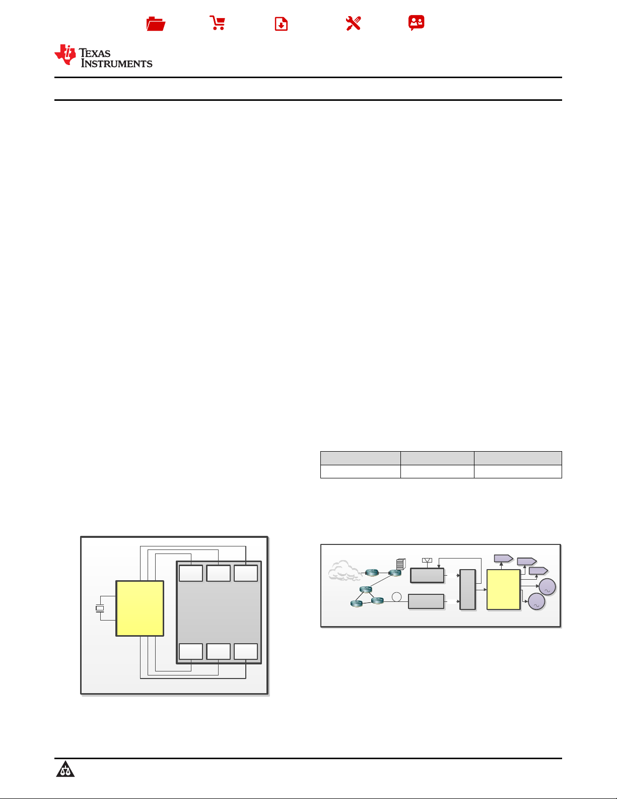
CDCM6208
Synthesizer
Mode
TMS320TCI6616/18
DSP
AIF ALT
CORE
SRIO
PCIePacket
Accel
DR
Base Band DSP
Clocking
Pico Cell Clocking
DPLL
CDCM6208
APLL
GPS receiver
IEEE1588
timing extract
Ethernet
SyncE
Ethernet
Timing
Server
1pps
1pps
Core
Packet
network
FBADC
RXADC
TXDAC
RF LO
RF LO
Product
Folder
Sample &
Buy
Technical
Documents
Tools &
Software
Support &
Community
CDCM6208V1F 2:8 Clock Generator, Jitter Cleaner with Fractional Dividers
1 Features 2 Applications
1
• Superior Performance with Low Power:
– Low Noise Synthesizer (265 fs-rms Typical
Jitter) or Low Noise Jitter Cleaner (1.6 ps-rms
Typical Jitter)
– 0.5 W Typical Power Consumption
– High Channel-to-Channel Isolation and
Excellent PSRR
– Device Performance Customizable Through
Flexible 1.8 V, 2.5 V and 3.3 V Power
Supplies, Allowing Mixed Output Voltages
• Flexible Frequency Planning:
– 4x Integer Down-divided Differential Clock
Outputs Supporting LVPECL-like, CML, or
LVDS-like Signaling
– 4x Fractional or Integer Divided Differential
Clock Outputs Supporting HCSL, LVDS-like
Signaling, or Eight CMOS Outputs
– Fractional Output Divider Achieve 0 ppm to < 1
ppm Frequency Error and Eliminates need for
Crystal Oscillators and Other Clock Generators
– Output frequencies up to 800 MHz
• Two Differential Inputs, XTAL Support, Ability for
Smart Switching
• SPI, I2C™, and Pin Programmable
• Professional user GUI for Quick Design
Turnaround
• 7 x 7 mm 48-QFN package (RGZ)
• -40 °C to 85 °C temperature range
• Base Band Clocking (Wireless Infrastructure)
• Networking and Data Communications
• Keystone C66x Multicore DSP Clocking
• Storage Server, Portable Test Equipment,
• Medical Imaging, High End A/V
3 Description
The CDCM6208V1F is a highly versatile, low jitter,
low-power frequency synthesizer that can generate
eight low jitter clock outputs, selectable between
LVPECL-like high-swing CML, normal-swing CML,
LVDS-like low-power CML, HCSL, or LVCMOS, from
one of two inputs that can feature a low frequency
crystal or CML, LVPECL, LVDS, or LVCMOS signals
for a variety of wireless infrastructure baseband,
wireline data communication, computing, low power
medical imaging and portable test and measurement
applications. The CDCM6208V1F also features an
innovative fractional divider architecture for four of its
outputs that can generate any frequency with better
than 1ppm frequency accuracy. The CDCM6208V1F
can be easily configured through I2C or SPI
programming interface and in the absence of serial
interface, pin mode is also available that can set the
device in 1 of 32 distinct pre-programmed
configurations using control pins.
Device Information
PART NUMBER PACKAGE BODY SIZE (NOM)
CDCM6208V1F VQFN (48) 7.00 mm × 7.00 mm
(1) For all available packages, see the orderable addendum at
the end of the datasheet.
CDCM6208V1F
SCAS943 –MAY 2015
(1)
4 Simplified Schematics
1
An IMPORTANT NOTICE at the end of this data sheet addresses availability, warranty, changes, use in safety-critical applications,
intellectual property matters and other important disclaimers. PRODUCTION DATA.
CDCM6208V1F
SCAS943 –MAY 2015
www.ti.com
Table of Contents
1 Features.................................................................. 1
2 Applications ........................................................... 1
3 Description ............................................................. 1
4 Simplified Schematics........................................... 1
5 Revision History..................................................... 2
6 Description (continued)......................................... 3
7 Pin Configuration and Functions......................... 3
8 Specifications......................................................... 6
8.1 Absolute Maximum Ratings ..................................... 6
8.2 ESD Ratings.............................................................. 6
8.3 Recommended Operating Conditions....................... 7
8.4 Thermal Information, Airflow = 0 LFM ..................... 7
8.5 Thermal Information, Airflow = 150 LFM ................. 8
8.6 Thermal Information, Airflow = 250 LFM ................. 8
8.7 Thermal Information, Airflow = 500 LFM ................. 8
8.8 Single Ended Input Characteristics .......................... 9
8.9 Single Ended Input Characteristics (PRI_REF,
SEC_REF) ................................................................. 9
8.10 Differential Input Characteristics (PRI_REF,
SEC_REF) ............................................................... 10
8.11 Crystal Input Characteristics (SEC_REF) ............. 10
8.12 Single Ended Output Characteristics (STATUS1,
STATUS0, SDO, SDA) ............................................ 11
8.13 PLL Characteristics............................................... 11
8.14 LVCMOS Output Characteristics .......................... 12
8.15 LVPECL (High-Swing CML) Output
Characteristics ......................................................... 13
8.16 CML Output Characteristics.................................. 13
8.17 LVDS (Low-Power CML) Output Characteristics. 14
8.18 HCSL Output Characteristics............................... 14
8.19 Output Skew and Sync to Output Propagation Delay
Characteristics ......................................................... 15
8.20 Device Individual Block Current Consumption...... 16
8.21 Worst Case Current Consumption........................ 17
8.22 I2C TIMING .......................................................... 18
8.23 SPI Timing Requirements ..................................... 19
8.24 Typical Characteristics ......................................... 20
9 Parameter Measurement Information................ 22
9.1 Characterization Test Setup ................................... 22
10 Detailed Description ........................................... 28
10.1 Overview............................................................... 28
10.2 Functional Block Diagram ..................................... 28
10.3 Feature Description............................................... 29
10.4 Device Functional Modes...................................... 30
10.5 Programming......................................................... 38
10.6 Register Maps....................................................... 42
11 Application and Implementation........................ 53
11.1 Application Information.......................................... 53
11.2 Typical Applications .............................................. 53
12 Power Supply Recommendations..................... 72
12.1 Power Rail Sequencing, Power Supply Ramp Rate,
and Mixing Supply Domains .................................... 72
13 Layout................................................................... 74
13.1 Layout Guidelines ................................................. 74
13.2 Layout Example .................................................... 74
14 Device and Documentation Support................. 80
14.1 Trademarks........................................................... 80
14.2 Documentation Support ....................................... 80
14.3 Electrostatic Discharge Caution............................ 80
14.4 Glossary................................................................ 80
15 Mechanical, Packaging, and Orderable
Information........................................................... 80
5 Revision History
DATE REVISION NOTES
May 2015 * Initial release.
2 Submit Documentation Feedback Copyright © 2015, Texas Instruments Incorporated
Product Folder Links: CDCM6208V1F
48
VDD_PLL1
47
RESETN/PWR
46
PDN
45
SYNCN
44
Y7_N
43
Y7_P
42
41
VDD_Y7
40
Y6_N
39
Y6_P
38
VDD_Y6
VDD_Y5
36
37
35
34
33
STATUS0
STATUS1/PIN0
ELF
17
18
19
20
21
22
23
24
28
27
26
29
25
30
31
32
Y0_P
Y1_N
Y1_P
VDD_Y0_Y1
VDD_Y2_Y3
Y2_P
Y2_N
VDD_Y0_Y1
SDI/SDA/PIN1
SDO/AD0/PIN2
SCS/AD1/PIN3
REF_SEL
SCL/PIN4
1
2
3
4
5
6
7
8
9
10
11
131214
15
16
Y5_P
PRI_REFN
Y0_N
PRI_REFP
SI_MODE0
Y4_N
Y3_N
REG_CAP
VDD_VCO
SEC_REFP
SEC_REFN
Y3_P
VDD_Y2_Y3
Y4_P
VDD_Y4
Y5_N
VDD_PLL2
SI_MODE1
DVDD
DVDD
VDD VDD_Y 2_Y3
VDD_Y4
VDD_Y5
VDD_Y6
VDD_Y7
VDD_PRI_REF
VDD_SECI_REF
VDD_SEC_REF
_Y0_Y1
VDD_PRI_REF
CDCM6208V1F
www.ti.com
SCAS943 –MAY 2015
6 Description (continued)
In synthesizer mode, the overall output jitter performance is less than 0.5 ps-rms (10 k - 20 MHz) or 20 ps-pp
(unbound) on output using integer dividers and is between 50 to 220 ps-pp (10 k - 40 MHz) on outputs using
fractional dividers depending on the prescaler output frequency.
In jitter cleaner mode, the overall output jitter is less than 2.1 ps-rms (10 k - 20 MHz) or 40 ps-pp on output
using integer dividers and is less than 70 ps to 240 ps-pp on outputs using fractional dividers. The
CDCM6208V1F is packaged in a small 48-pin 7 mm x 7 mm QFN package.
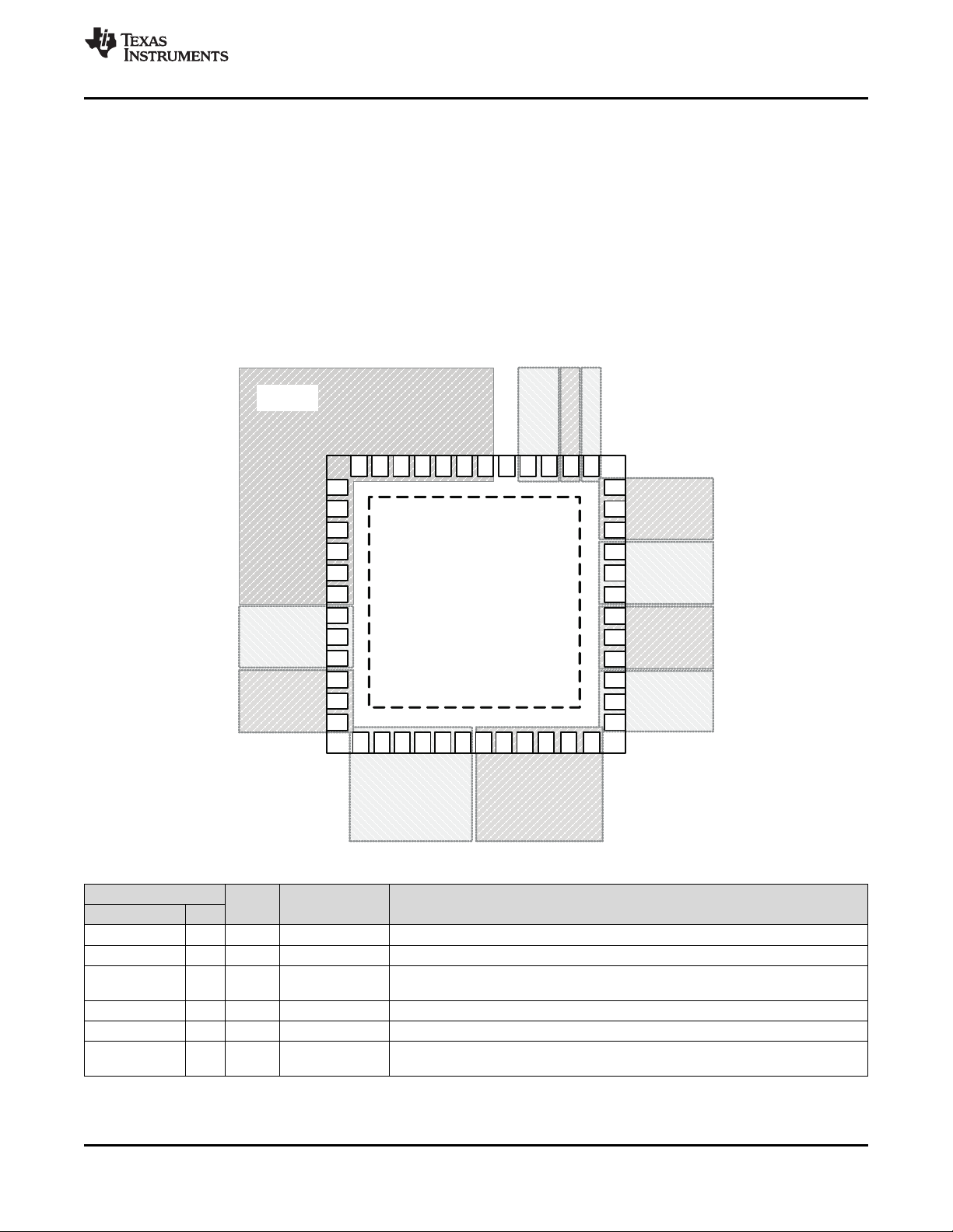
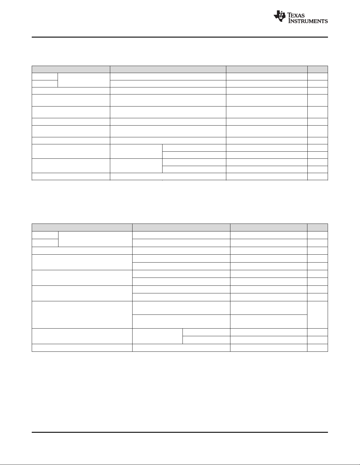
7 Pin Configuration and Functions
RGZ Package
48 Pin VQFN
Top View
PIN
NAME NO.
PRI_REFP 8 Input Universal Primary Reference Input +
PRI_REFN 9 Input Universal Primary Reference Input –
VDD_PRI_REF 7 PWR Analog
SEC_REFP 11 Input Universal Secondary Reference Input +
SEC_REFN 12 Input Universal Secondary Reference Input –
VDD_SEC_REF 10 PWR Analog
(1) If Secondary input buffer is disabled (Register 4 Bit 5 = 0), it is possible to connect VDD_SEC_REF to GND.
Copyright © 2015, Texas Instruments Incorporated Submit Documentation Feedback 3
I/O TYPE DESCRIPTION
Product Folder Links: CDCM6208V1F
Pin Functions
Supply pin for reference inputs to set between 1.8 V, 2.5 V, or 3.3 V or connect to
VDD_SEC_REF.
Supply pin for reference inputs to set between 1.8 V, 2.5 V, or 3.3 V or connect to
VDD_PRI_REF
(1)
.
CDCM6208V1F
SCAS943 –MAY 2015
Pin Functions (continued)
PIN
NAME NO.
REF_SEL 6 Input
ELF 41 Output Analog External loop filter pin for PLL
Y0_P 14 Output Universal Output 0 Positive Terminal
Y0_N 15 Output Universal Output 0 Negative Terminal
Y1_P 17 Output Universal Output 1 Positive Terminal
Y1_N 16 Output Universal Output 1 Negative Terminal
VDD_Y0_Y1 (2 13,
pins) 18
Y2_P 20 Output Universal Output 2 Positive Terminal
Y2_N 21 Output Universal Output 2 Negative Terminal
Y3_P 23 Output Universal Output 3 Positive Terminal
Y3_N 22 Output Universal Output 3 Negative Terminal
VDD_Y2_Y3 (2 19,
pins) 24
Y4_P 26 Output Universal Output 4 Positive Terminal
Y4_N 25 Output Universal Output 4 Negative Terminal
VDD_Y4 27 PWR Analog Supply pin for output 4 to set between 1.8 V, 2.5 V or 3.3 V
Y5_P 29 Output Universal Output 5 Positive Terminal
Y5_N 28 Output Universal Output 5 Negative Terminal
VDD_Y5 30 PWR Analog Supply pin for output 5 to set between 1.8 V, 2.5 V or 3.3 V
Y6_P 32 Output Universal Output 6 Positive Terminal
Y6_N 33 Output Universal Output 6 Negative Terminal
VDD_Y6 31 PWR Analog Supply pin for output 6 to set between 1.8 V, 2.5 V or 3.3 V
Y7_P 35 Output Universal Output 7 Positive Terminal
Y7_N 36 Output Universal Output 7 Negative Terminal
VDD_Y7 34 PWR Analog Supply pin for output 7 to set between 1.8 V, 2.5 V or 3.3 V
VDD_VCO 39 PWR Analog supply of this pin and the VDD_PLL2 supply pin can be combined as they are both
VDD_PLL1 37 PWR Analog Analog Power Supply Connections
VDD_PLL2 38 PWR Analog supply of VDD_PLL2 and VDD_VCO can be combined as these pins are both
DVDD 48 PWR Analog
GND PAD PWR Analog Power Supply Ground and Thermal Pad
STATUS0 46 Output LVCMOS Status pin 0 (see Table 7 for details)
STATUS1/PIN0 45 and
SI_MODE1 47 Input mode;SI_MODE[1:0]=01: I2C mode;SI_MODE[1:0]=10: Pin Mode (No serial
SI_MODE0 1
SDI/SDA/PIN1 2 I/O
I/O TYPE DESCRIPTION
LVCMOS selection is also controlled through Register 4 bit 12.REF_SEL = 0 (≤ VIL): selects
w/ 50kΩ pull-up PRI_REFREF_SEL = 1 (≥ VIH): selects SEC_REF (when Reg 4.12 = 1). See
PWR Analog Supply pin for outputs 0, 1 to set between 1.8 V, 2.5 V or 3.3 V
PWR Analog Supply pin for outputs 2, 3 to set between 1.8 V, 2.5 V or 3.3 V
Output
Input
LVCMOS STATUS1: Status pin in SPI/I2C modes. For details see Table 6 for pin modes and
no pull resistor Table 7 for status mode. PIN0: Control pin 0 in pin mode.
LVCMOSw
50kΩ pull-up
LVCMOSw
50kΩ pull-down
LVCMOS in
Open drain out SDI: SPI Serial Data Input SDA: I2C Serial Data (Read/Write bi-directional), open
LVCMOS in drain output; requires a pull-up resistor in I2C mode;PIN1: Control pin 1 in pin mode
no pull resistor
Manual Reference Selection MUX for PLL. In SPI or I2C mode the reference
Table 36 for detail.
Analog power supply for PLL/VCO; This pin is sensitive to power supply noise; The
analog and sensitive supplies;
Analog Power Supply Connections; This pin is sensitive to power supply noise; The
power-sensitive, analog supply pins
Digital Power Supply Connections; This is also the reference supply voltage for all
control inputs and must match the expected input signal swing of control inputs.
Serial Interface Mode or Pin mode selection.SI_MODE[1:0]=00: SPI
programming);SI_MODE[1:0]=11: RESERVED
www.ti.com
4 Submit Documentation Feedback Copyright © 2015, Texas Instruments Incorporated
Product Folder Links: CDCM6208V1F

CDCM6208V1F
www.ti.com
SCAS943 –MAY 2015
Pin Functions (continued)
PIN
NAME NO.
SDO/AD0/PIN2 3
SCS/AD1/PIN 3 4 Input
SCL/PIN4 5 Input SCL: SPI/I2C ClockPIN4: Control pin 4 in pin mode
RESETN/PWR 44 Input up).
REG_CAP 40 Output Analog
PDN 43 Input the entire device and defaults all registers. It is recommended to connect a capacitor
SYNCN 42 Input
(2) Note: the device cannot be programmed in I2C while RESETN is held low.
I/O TYPE DESCRIPTION
LVCMOS out
Output/I LVCMOS in SDO: SPI Serial Data AD0: I2C Address Offset Bit 0 inputPIN2: Control pin 2 in pin
nput LVCMOS in mode
no pull resistor
LVCMOS no pull SCS: SPI Latch EnableAD1: I2C Address Offset Bit 1 inputPIN3: Control pin 3 in pin
resistor mode
LVCMOS no pull
resistor
In SPI/I2C programming mode, external RESETN signal (active low).
RESETN = VIL: device in reset (registers values are retained)
RESETN = VIH: device active. The device can be programmed via SPI while
LVCMOS
w/ 50kΩ pull-up
RESETN is held low (this is useful to avoid any false output frequencies at power
(2)
In Pin mode this pin controls device core and I/O supply voltage setting. 0 = 1.8 V, 1
= 2.5/3.3 V for the device core and I/O power supply voltage. In pin mode, it is not
possible to mix and match the supplies. All supplies should either be 1.8 V or 2.5/3.3
V.
Regulator Capacitor; connect a 10 µF cap with ESR below 1 Ω to GND at
frequencies above 100 kHz
Power Down Active low. When PDN = VIHis normal operation. When PDN = VIL, the
LVCMOS
w/ 50kΩ pull-up
device is disabled and current consumption minimized. Exiting power down resets
to GND to hold the device in power-down until the digital and PLL related power
supplies are stable. See section on power down in the application section.
LVCMOS Active low. Device outputs are synchronized on a low-to-high transition on the
w/ 50kΩ pull-up SYNCN pin. SYNCN held low disables all outputs.
Copyright © 2015, Texas Instruments Incorporated Submit Documentation Feedback 5
Product Folder Links: CDCM6208V1F
CDCM6208V1F
SCAS943 –MAY 2015
8 Specifications
www.ti.com
8.1 Absolute Maximum Ratings
(1)
over operating free-air temperature range (unless otherwise noted)
PARAMETER MIN MAX UNIT
Supply Voltage Range, VDD_PRI, VDD_SEC, VDD_Yx_Yy, VDD_PLL[2:1], DVDD -0.5 4.6 V
4.6
Input Voltage Range CMOS control inputs, V
IN
-0.5 and V
V
+ 0.5
DVDD
4.6
Input Voltage Range PRI/SEC inputs and V
Output Voltage Range, V
Input Current, I
IN
Output Current, I
Junction Temperature, T
OUT
OUT
J
Storage temperature range, T
V
VDDPRI.SEC
-0.5 V
stg
-65 150 °C
+ 0.5
+ 0.5 V
YxYy
20 mA
50 mA
125 °C
(1) Stresses beyond those listed under "absolute maximum ratings" may cause permanent damage to the device. These are stress ratings
only and functional operation of the device at these or any other conditions beyond those indicated under "recommended operating
conditions" is not implied. Exposure to absolute—maximum—rated conditions for extended periods may affect device reliability.
8.2 ESD Ratings
VALUE UNIT
Human body model (HBM), per ANSI/ESDA/JEDEC JS-001, all pins
V
(ESD)
Electrostatic discharge V
Charged device model (CDM), per JEDEC specification JESD22-C101, all
(2)
pins
(1) JEDEC document JEP155 states that 500-V HBM allows safe manufacturing with a standard ESD control process.
(2) JEDEC document JEP157 states that 250-V CDM allows safe manufacturing with a standard ESD control process.
(1)
±2000
±500
6 Submit Documentation Feedback Copyright © 2015, Texas Instruments Incorporated
Product Folder Links: CDCM6208V1F
CDCM6208V1F
www.ti.com
SCAS943 –MAY 2015
8.3 Recommended Operating Conditions
over operating free-air temperature range (unless otherwise noted)
MIN NOM MAX UNIT
VDD_Yx_Yy Output Supply Voltage 1.71 1.8/2.5/3.3 3.465 V
VDD_PLL1
VDD_PLL2
DVDD Core Digital Supply Voltage 1.71 1.8/2.5/3.3 3.465 V
VDD_PRI,
VDD_SEC
ΔVDD/Δt 50 < t
T
A
SDA and SCL in I2C MODE (SI_MODE[1:0] = 01)
V
I
d
R
V
IH
V
IL
C
BUS_I2C
(1) For fast power up ramps under 50 ms and when all supply pins are driven from the same power supply source, PDN can be left floating.
For slower power up ramps or if supply pins are sequenced with uncertain time delays, PDN needs to be held low until DVDD,
VDD_PLLx, and VDD_PRI/SEC reach at least 1.45V supply voltage. See application section on mixing power supplies and particularly
Figure 58 for details.
Core Analog Supply Voltage 1.71 1.8/2.5/3.3 3.465 V
Reference Input Supply Voltage 1.71 1.8/2.5/3.3 3.465 V
VDD power-up ramp time (0 to 3.3 V) PDN left open, all VDD tight
together PDN low-high is delayed
(1)
PDN
ms
Ambient Temperature -40 85 °C
Input Voltage
Data Rate kbps
High-level input voltage V
DVDD = 1.8 V –0.5 2.45 V
DVDD = 3.3 V –0.5 3.965 V
100
400
0.7 x
DVDD
Low-level input voltage 0.3 x DVDD V
Total capacitive load for each bus line 400 pF
8.4 Thermal Information, Airflow = 0 LFM
(1) (2) (3) (4)
CDCM6208
THERMAL METRIC
(1)
RGZ UNIT
48 PINS VQFN
R
θJA
R
θJC(top)
R
θJB
ψ
JT
ψ
JB
R
θJC(bot)
Junction-to-ambient thermal resistance 30.27
Junction-to-case (top) thermal resistance 16.58
Junction-to-board thermal resistance 6.83
Junction-to-top characterization parameter 0.23
Junction-to-board characterization parameter 6.8
Junction-to-case (bottom) thermal resistance 1.06
°C/W
(1) For more information about traditional and new thermal metrics, see the IC Package Thermal Metrics application report, SPRA953.
(2) The package thermal resistance is calculated in accordance with JESD 51 and JEDEC2S2P (high-k board).
(3) Connected to GND with 36 thermal vias (0.3 mm diameter).
(4) θJB(junction to board) is used for the QFN package, the main heat flow is from the junction to the GND pad of the QFN.
Copyright © 2015, Texas Instruments Incorporated Submit Documentation Feedback 7
Product Folder Links: CDCM6208V1F
CDCM6208V1F
SCAS943 –MAY 2015
www.ti.com
8.5 Thermal Information, Airflow = 150 LFM
(1) (2) (3) (4)
CDCM6208
THERMAL METRIC
(1)
RGZ UNIT
48 PINS
R
θJA
R
θJC(top)
R
θJB
ψ
JT
ψ
JB
R
θJC(bot)
Junction-to-ambient thermal resistance 21.8
Junction-to-case (top) thermal resistance
Junction-to-board thermal resistance 6.61
Junction-to-top characterization parameter 0.37
Junction-to-board characterization parameter
Junction-to-case (bottom) thermal resistance 1.06
°C/W
(1) For more information about traditional and new thermal metrics, see the IC Package Thermal Metrics application report, SPRA953.
(2) The package thermal resistance is calculated in accordance with JESD 51 and JEDEC2S2P (high-k board).
(3) Connected to GND with 36 thermal vias (0.3 mm diameter).
(4) θJB(junction to board) is used for the QFN package, the main heat flow is from the junction to the GND pad of the QFN.
8.6 Thermal Information, Airflow = 250 LFM
(1) (2) (3) (4)
CDCM6208
THERMAL METRIC
(1)
RGZ UNIT
48 PINS
R
θJA
R
θJC(top)
R
θJB
ψ
JT
ψ
JB
R
θJC(bot)
Junction-to-ambient thermal resistance 19.5
Junction-to-case (top) thermal resistance
Junction-to-board thermal resistance 6.6
Junction-to-top characterization parameter 0.45
Junction-to-board characterization parameter
Junction-to-case (bottom) thermal resistance 1.06
°C/W
(1) For more information about traditional and new thermal metrics, see the IC Package Thermal Metrics application report, SPRA953.
(2) The package thermal resistance is calculated in accordance with JESD 51 and JEDEC2S2P (high-k board).
(3) Connected to GND with 36 thermal vias (0.3 mm diameter).
(4) θJB(junction to board) is used for the QFN package, the main heat flow is from the junction to the GND pad of the QFN.
8.7 Thermal Information, Airflow = 500 LFM
(1) (2) (3) (4)
CDCM6208
THERMAL METRIC
(1)
RGZ UNIT
48 PINS
R
θJA
R
θJC(top)
R
θJB
ψ
JT
ψ
JB
R
θJC(bot)
Junction-to-ambient thermal resistance 17.7
Junction-to-case (top) thermal resistance
Junction-to-board thermal resistance 6.58
Junction-to-top characterization parameter 0.58
Junction-to-board characterization parameter
Junction-to-case (bottom) thermal resistance 1.05
°C/W
(1) For more information about traditional and new thermal metrics, see the IC Package Thermal Metrics application report, SPRA953.
(2) The package thermal resistance is calculated in accordance with JESD 51 and JEDEC2S2P (high-k board).
(3) Connected to GND with 36 thermal vias (0.3 mm diameter).
(4) θJB(junction to board) is used for the QFN package, the main heat flow is from the junction to the GND pad of the QFN.
8 Submit Documentation Feedback Copyright © 2015, Texas Instruments Incorporated
Product Folder Links: CDCM6208V1F
CDCM6208V1F
www.ti.com
SCAS943 –MAY 2015
8.8 Single Ended Input Characteristics
(SI_MODE[1:0], SDI/SDA/PIN1, SCL/PIN4, SDO/ADD0/PIN2, SCS/ADD1/PIN3, STATUS1/PIN0, RESETN/PWR, PDN,
SYNCN, REF_SEL), DVDD = 1.71V to 1.89V, 2.375V to 2.625V, 3.135V to 3.465V, TA= –40°C to 85°C
PARAMETER TEST CONDITIONS MIN TYP MAX UNIT
V
IH
V
IL
I
IH
I
IL
ΔV/ΔT 20% - 80% 0.75 V/ns
minPulse 10 ns
C
IN
RESETN, PWR, SYNCN, PDN, REF_SEL, SI_MODE[1:0]:
R Input Pullup and Pulldown Resistor 35 50 65 kΩ
SDA and SCL in I2C Mode (SI_MODE[1:0]=01)
V
HYS_I2C
I
H
V
OL
C
IN
Input High Voltage 0.8 x DVDD V
Input Low Voltage 0.2 x DVDD V
Input High Current 30 µA
DVDD = 3.465V, VIH= 3.465 V (pull-up
resistor excluded)
Input Low Current DVDD = 3.465V, VIL= 0 V -30 µA
PDN, RESETN, SYNCN, REF_SEL Input
Edge Rate
PDN, RESETN, SYNCN low pulse to
trigger proper device reset
Input Capacitance 2.25 pF
Input hysteresis
DVDD = 1.8 V 0.1 V
DVDD = 2.5/3.3 V 0.05 V
DVDD
DVDD
High-level input current VI= DVDD –5 5 µA
Output Low Voltage IOL= 3mA 0.2 x DVDD V
Input Capacitance terminal 5 pF
V
V
8.9 Single Ended Input Characteristics (PRI_REF, SEC_REF)
VDD_PRI, VDD_SEC = 1.71 V to 1.89 V, 2.375 V to 2.625 V, 3.135 V to 3.465 V, TA= –40°C to 85°C
PARAMETER TEST CONDITIONS MIN TYP MAX UNIT
f
IN
V
V
V
I
IH
I
IL
IH
IL
HYST
Reference and Bypass Input
Frequency
Input High Voltage VDD_PRI/V V
Input Low Voltage VDD_PRI/V V
Input hysteresis 20 65 150 mV
Input High Current VDD_PRI/VDD_SEC = 3.465 V, VIH= 3.465 V 30 µA
Input Low Current VDD_PRI/VDD_SEC = 3.465 V, VIL= 0 V -30 µA
ΔV/ΔT Reference Input Edge Rate 20% - 80% 0.75 V/ns
IDC
C
SE
IN
Reference Input Duty Cycle
Input Capacitance 2.25 pF
VDD_PRI/SEC = 1.8 V 0.008 200 MHz
VDD_PRI/SEC = 3.3 V 0.008 250 MHz
0.8 x
DD_SEC
0.2 x
DD_SEC
f
≤ 200MHz 40% 60%
PRI
200 ≤ f
≤ 250 MHz 43% 60%
PRI
Copyright © 2015, Texas Instruments Incorporated Submit Documentation Feedback 9
Product Folder Links: CDCM6208V1F
CDCM6208V1F
SCAS943 –MAY 2015
www.ti.com
8.10 Differential Input Characteristics (PRI_REF, SEC_REF)
VDD_PRI, VDD_SEC = 1.71 V to 1.89 V, 2.375 V to 2.625 V, 3.135 V to 3.465 V, TA= –40°C TO 85°C
PARAMETER TEST CONDITIONS MIN TYP MAX UNIT
f
IN
V
I
V
ICM
V
ICM
V
HYST
I
IH
I
IL
ΔV/ΔT Reference Input Edge Rate 20% - 80% 0.75 V/ns
IDC
DIFF
C
IN
Reference and Bypass Input Frequency 0.008 250 MHz
Differential Input Voltage Swing, Peak-to-
Peak
Input Common Mode Voltage CML input signaling, R4[7:6] = 00 DD_SEC- DD_SEC- V
Input Common Mode Voltage 0.8 1.2 1.5 V
Input hysteresis
Input High Current VDD_PRI/SEC = 3.465 V, VIH= 3.465 V 30 µA
Input Low Current VDD_PRI/SEC = 3.465V, VIL= 0 V -30 µA
Reference Input Duty Cycle 30% 70%
Input Capacitance 2.7 pF
VDD_PRI/SEC = 2.5/3.3 V 0.2 1.6 V
VDD_PRI/SEC = 1.8 V 0.2 1 V
VDD_PRI/V VDD_PRI/V
0.4 0.1
LVDS, VDD_PRI/SEC
= 1.8/2.5/3.3 V,
R4[7:6] = 01, R4.1 = d.c.,
R4.0 = d.c.
LVDS (Q4[7:6,4:3] = 01) 15 65 mV
CML (Q4[7:6,4:3] = 00) 20 85 mV
8.11 Crystal Input Characteristics (SEC_REF)
VDD_SEC = 1.71 to 1.89 V, 2.375 V to 2.625 V, 3.135 V to 3.465 V,TA= –40°C to 85°C
PARAMETER MIN TYP MAX UNIT
MODE OF OSCILLATION FUNDAMENTAL
Frequency
See note
See note
10 MHz 150
Equivalent Series Resistance (ESR) 25 MHz 70
50 MHz 30
1.8 V / 3.3 V SEC_REFP 3.5 4.5 5.5
On-chip load capacitance 1.8 V SEC_REFN 5.5 7.25 8.5 pF
3.3 V SEC_REFN 6.5 7.34 8.5
Drive Level See note
(1) Verified with crystals specified for a load capacitance of CL=8pF, the pcb related capacitive load was estimated to be 2.3pF, and
completed with a load capacitors of 4pF on each crystal terminal connected to GND. XTALs tested: NX3225GA 10MHz EXS00ACG02813 CRG, NX3225GA 19.44MHz EXS00A-CG02810 CRG, NX3225GA 25MHz EXS00A-CG02811 CRG, and NX3225GA
30.72MHz EXS00A-CG02812 CRG.
(2) For 30.73 MHz to 50 MHz, it is recommended to verify sufficient negative resistance and initial frequency accuracy with the crystal
vendor. The 50 MHz use case was verified with a NX3225GA 50MHz EXS00A-CG02814 CRG. To meet a minimum frequency error, the
best choice of the XTAL was one with CL= 7pF instead of CL= 8pF.
(3) With NX3225GA_10M the measured remaining negative resistance on the EVM is 6430 Ω (43 x margin)
(4) With NX3225GA_25M the measured remaining negative resistance on the EVM is 1740 Ω (25 x margin)
(5) With NX3225GA_50M the measured remaining negative resistance on the EVM is 350 Ω (11 x margin)
(6) Maximum drive level measured was 145 µW; XTAL should at least tolerate 200 µW
(1)
(2)
(6)
10 30.72 MHz
30.73 50 MHz
(3)
(4)
(5)
200 µW
PP
PP
pp
pp
Ω
10 Submit Documentation Feedback Copyright © 2015, Texas Instruments Incorporated
Product Folder Links: CDCM6208V1F
CDCM6208V1F
www.ti.com
SCAS943 –MAY 2015
8.12 Single Ended Output Characteristics (STATUS1, STATUS0, SDO, SDA)
VDD_Yx_Yy, VDD_PRI, VDD_SEC, VDD_PLLx, DVDD, VDD_VCO = 1.71V to 1.89V, 2.375V to 2.625V, 3.135V to 3.465V;
TA= –40°C to 85°C (Output load capacitance 10 pF unless otherwise noted)
PARAMETER TEST CONDITIONS MIN TYP MAX UNIT
Status 1, Status 0, and SDO only;
V
OH
V
OL
V
slew
I
OZH
I
OZL
t
LOS
t
LOCK
Output High Voltage V
Output Low Voltage IOL= 1 mA V
Output slew rate 30% - 70% 0.5 V/ns
3-stat Output High Current DVDD = 3.465 V, VIH= 3.465 V 5 µA
3-stat Output Low Current DVDD = 3.465 V, VIL= 0 V -5 µA
Status Loss of Signal Detection
Time
Status PLL Lock Detection Time 1/f
SDA is open drain and relies on 0.8 x
external pullup for high output; IOH= DVDD
1 mA
0.2 x
DVDD
LOS_REFfvco 1 2 1/f
Detect lock 2304
Detect unlock 512
PFD
PFD
8.13 PLL Characteristics
VDD_PLLx, VDD_VCO = 1.71 V to 1.89 V, 2.375 V to 2.625 V, 3.135 V to 3.465 V, TA= –40°C TO 85°C
PARAMETER TEST CONDITIONS MIN TYP MAX UNIT
f
VCO
K
VCO
f
PFD
I
CP-L
f
FOM
t
STARTUP
VCO Frequency Range 2.39 2.55 GHz
2.39 GHz 178
VCO Gain 2.50 GHz 204 MHz/V
2.55 GHz 213
PFD Input Frequency 0.008 100 MHz
High Impedance Mode Charge
Pump Leakage
Estimated PLL Figure of Merit
(FOM)
Measured in-band phase noise at
the VCO output minus 20log(N- –224 dBc/Hz
divider) at the flat region
±700 nA
Power supply ramp time of 1ms from
0 V to 1.7 V, final frequency
Startup time (see Figure 42 )
accuracy of 10 ppm, f
C
PDN_to_GND
= 22nF
= 25 MHz,
PFD
w/ PRI input signal 12.8 ms
w/ NDK 25 MHz crystal 12.85 ms
Copyright © 2015, Texas Instruments Incorporated Submit Documentation Feedback 11
Product Folder Links: CDCM6208V1F
CDCM6208V1F
SCAS943 –MAY 2015
www.ti.com
8.14 LVCMOS Output Characteristics
VDD_Yx_Yy = 1.71 V to 1.89V, 2.375 V to 2.625 V, 3.135 V to 3.465 V, TA= –40°C TO 85°C
PARAMETER TEST CONDITIONS MIN TYP MAX UNIT
Fract Out divVDD_Yx_Yy = 2.5/3.3 V 0.78 250
f
OUT-F
f
ACC-F
V
OH
V
OL
V
OH
V
OL
I
OH
I
OL
t
SLEW-RATE-N
t
SLEW-RATE-S
PN-floor Phase Noise Floor f
ODC Output Duty Cycle Not in bypass mode 45% 55%
R
OUT
(1) The User's GUI calculates exact frequency error. It is a fixed, static offset. If the desired output target frequency is with the exact reach
of a multiple 1 over 220, the actual output frequency error is 0.
Note: In LVCMOS Mode, positive and negative outputs are in phase.
Output Frequency Integer out divVDD_Yx_Yy = 2.5/3.3 V 1.55 250 MHz
Int or frac out divVDD_Yx_Yy = 1.8 V 0.78/1.5 200
Output Frequency Error
Output High Voltage (normal mode) VDD_Yx = min to max, IOH= -1 mA V
Output Low Voltage(normal mode) VDD_Yx = min to max, IOL= 100 µA V
Output High Voltage (slow mode) VDD_Yx = min to max, IOH= -100 µA V
Output Low Voltage(slow mode) VDD_Yx = min to max, IOL= 100 µA V
(1)
Fractional Output Divider –1 1 ppm
0.8 x
VDD_Yx_Yy
0.2 x
VDD_Yx_Yy
0.7 x
VDD_Yx_Yy
0.3 x
VDD_Yx_Yy
V
= VDD_Yx_Yy/2
OUT
Output High Current Normal mode –50 -8 mA
Slow mode –45 -5 mA
V
= VDD_Yx_Yy/2
OUT
Output Low Current Normal mode 10 55 mA
Slow mode 5 40 mA
Output Rise/Fall Slew Rate (normal
mode)
Output Rise/Fall Slew Rate (normal
mode)
Output Rise/Fall Slew Rate (slow
mode)
Output Rise/Fall Slew Rate (slow
mode)
Output Impedance
20% to 80%, VDD_Yx_Yy = 2.5/3.3 V,
CL= 5 pF
20% to 80%, VDD_Yx_Yy = 1.8 V,
CL= 5 pF
20% to 80%, VDD_Yx_Yy = 2.5/3.3 V,
CL= 5 pF
20% to 80%, VDD_Yx_Yy = 1.8 V,
CL= 5 pF
= 122.88 MHz –159.5 –154 dBc/Hz
OUT
V
= VDD_Yx/2
OUT
5.37 V/ns
2.62 V/ns
4.17 V/ns
1.46 V/ns
Normal mode 30 50 90
Slow mode 45 74 130
Ω
12 Submit Documentation Feedback Copyright © 2015, Texas Instruments Incorporated
Product Folder Links: CDCM6208V1F
CDCM6208V1F
www.ti.com
SCAS943 –MAY 2015
8.15 LVPECL (High-Swing CML) Output Characteristics
VDD_Yx_Yy = 1.71 V to 3.465 V, VDD_PRI, VDD_SEC, VDD_PLLx, DVDD, VDD_VCO = 1.71 V to 1.89 V, 2.375 V to 2.625
V, 3.135 V to 3.465 V, TA= –40°C TO 85°C
PARAMETER TEST CONDITIONS MIN TYP MAX UNIT
f
OUT-I
V
CM-DC
|VOD| Differential output voltage
V
OUT
tR/t
t
slew
PN-floor Phase noise floor VDD_Yx_Yy = 3.3 V (See Figure 54) –161.4 –155.8 dBc/Hz
ODC Output duty cycle Not in bypass mode 47.5% 52.5%
R
OUT
Output frequency Integer Output Divider 1.55 800 MHz
Output DC coupled common mode
voltage
DC coupled with 50 Ω external termination to VDD_Yx_Yy V
100 Ω diff load AC coupling (See Figure 12), f
≤ 250 MHz
OUT
VDD_Yx
_
Yy – 0.4
VDD_Yx_Yy ≤ 1.89 V 0.45 0.75 1.12 V
VDD_Yx_Yy ≥ 2.375 V 0.6 0.8 1.12 V
100 Ω diff load AC coupling (See Figure 12), f
≥ 250 MHz
OUT
VDD_Yx_Yy ≤ 1.89 V 0.73 V
VDD_Yx_Yy ≥ 2.375 V 0.55 0.75 1.12 V
Differential output peak-to-peak
voltage
Output rise/fall time
F
±200 mV around crossing point 109 217 ps
20% to 80% V
OD
2 x |VOD| V
211 ps
Output rise/fall slew rate 3.7 5.1 7.3 V/ns
Output impedance measured from pin to VDD_Yx_Yy 50 Ω
8.16 CML Output Characteristics
VDD_Yx_Yy, VDD_PRI, VDD_SEC, VDD_PLLx, DVDD, VDD_VCO = 1.71V to 1.89V, 2.375V to 2.625V, 3.135V to 3.465V,
TA= –40°C to 85°C
PARAMETER TEST CONDITIONS MIN TYP MAX UNIT
f
OUT-I
V
CM-AC
V
CM-DC
|VOD| Differential output voltage 100 Ω diff load AC coupling, (See Figure 12) 0.3 0.45 0.58 V
V
OUT
tR/t
F
PN-floor Phasenoise floor at > 5 Hz offset f
ODC Output duty cycle Not in bypass mode 47.5% 52.5%
R
OUT
Output frequency Integer Output Divider 1.55 800 MHz
Output AC coupled common
mode voltage
Output DC coupled common
mode voltage
Differential output peak-to-peak
voltage
Output rise/fall time 20% to 80%
AC coupled with 50 Ω receiver termination VDD_Yx_Yy – 0.46 V
DC coupled with 50 Ω on-chip termination
to VDD_Yx_Yy
VDD_Yx_Yy – 0.2 V
2 x |VOD| V
VDDYx = 1.8 V 100 151 300 ps
VDDYx = 2.5 V/3.3 V 100 143 200 ps
= 122.88 MHz
OUT
VDD_Yx_Yy = 1.8 V –161.2 –155.8 dBc/Hz
VDD_Yx_Yy = 3.3 V –161.2 –153.8 dBc/Hz
Output impedance measured from pin to VDD_Yx_Yy 50 Ω
Copyright © 2015, Texas Instruments Incorporated Submit Documentation Feedback 13
Product Folder Links: CDCM6208V1F
CDCM6208V1F
SCAS943 –MAY 2015
www.ti.com
8.17 LVDS (Low-Power CML) Output Characteristics
VDD_Yx_Yy, VDD_PRI, VDD_SEC, VDD_PLLx, DVDD, VDD_VCO = 1.71 V to 1.89 V, 2.375 V to 2.625 V, 3.135V to
3.465V, TA= –40°C to 85°C
PARAMETER TEST CONDITIONS MIN TYP MAX UNIT
f
OUT-I
f
OUT-F
f
ACC-F
V
CM-AC
V
CM-DC
|VOD| Differential output voltage 100 Ω diff load AC coupling, (See Figure 12) 0.247 0.34 0.454 V
V
OUT
tR/t
F
PN-floor Phase noise floor f
ODC Output duty cycle Not in bypass mode
R
OUT
Output frequency
Output frequency error
Output AC coupled
common mode voltage
Output DC coupled
common mode voltage
Differential output peak-topeak voltage
Output rise/fall time ±100mV around crossing point 300 ps
Output impedance Measured from pin to VDD_Yx_Yy 167 Ω
(1) The User's GUI calculates exact frequency error. It is a fixed, static offset. If the desired output target frequency is with the exact reach
of a multiple of 1 over 220, the actual output frequency error is 0.
Integer output divider 1.55 400 MHz
Fractional output divider 0.78 400 MHz
(1)
Fractional output divider -1 1 ppm
AC coupled with 50 Ω receiver termination VDD_Yx_Yy – 0.76 V
DC coupled with 50 Ω on-chip termination to VDD_Yx_Yy VDD_Yx_Yy – 0.13 V
2 x |VOD| V
= 122.88 MHz
OUT
VDD_Yx = 1.8 V –159.3 –154.5 dBc/Hz
VDD_Yx = 2.5/3.3 V –159.1 –154.9 dBc/Hz
Y[3:0] 47.5% 52.5%
Y[7:4] 45% 55%
8.18 HCSL Output Characteristics
VDD_Yx_Yy, VDD_PRI, VDD_SEC, VDD_PLLx, DVDD, VDD_VCO = 1.71 to 1.89 V, 2.375 V to 2.625 V,3.135 V to 3.465 V,
TA= –40°C to 85°C
PARAMETER TEST CONDITIONS MIN TYP MAX UNIT
f
OUT-I
f
OUT-F
f
ACC-F
V
CM
Output frequency
Output Frequency Error
(1)
Output Common Mode Voltage
|VOD| Differential Output Voltage
V
tR/t
OUT
F
Differential Output Peak-to-peak
Voltage
Output Rise/Fall Time ps
PN-floor Phase Noise Floor f
ODC Output Duty Cycle Not in bypass mode 45% 55%
(1) The User's GUI calculates exact frequency error. It is a fixed, static offset. If the desired output target frequency is with the exact reach
of A 1/220multiple, the actual output frequency error is 0.
Integer Output Divider 1.55 400 MHz
Fractional Output Divider 0.78 400 MHz
Fractional Output Divider -1 1 ppm
VDD_Yx_Yy = 2.5/3.3 V 0.2 0.34 0.55 V
VDD_Yx_Yy = 1.8 V 0.2 0.33 0.55 V
VDD_Yx_Yy = 2.5/3.3 V 0.4 0.67 1.0 V
VDD_Yx_Yy = 1.8 V 0.4 0.65 1.0 V
VDD_Yx_Yy = 2.5/3.3 V 1.0 2.1 V
VDD_Yx_Yy = 1.8 V 2 x|VOD| V
Measured from V
V
= +100mV, VDD_Yx_Yy = 2.5/3.3 V
DIFF
Measured from V
V
= +100 mV, VDD_Yx_Yy = 1.8 V
DIFF
= 122.88 MHz
OUT
= –100 mV to
DIFF
= –100 mV to
DIFF
100 167 250
120 192 295
VDD_Yx_Yy = 1.8 V –158.8 –153 dBc/Hz
VDD_Yx = 2.5/3.3 V –157.6 –153 dBc/Hz
14 Submit Documentation Feedback Copyright © 2015, Texas Instruments Incorporated
Product Folder Links: CDCM6208V1F
CDCM6208V1F
www.ti.com
SCAS943 –MAY 2015
8.19 Output Skew and Sync to Output Propagation Delay Characteristics
VDD_Yx_Yy = 1.71 to 1.89 V, 2.375 V to 2.625 V, 3.135V to 3.465 V, TA= –40°C to 85°C
PARAMETER TEST CONDITIONS MIN TYP MAX UNIT
t
PD-PS
Propagation delay SYNCN↑ to output
toggling high
f
= 2.5 GHz PS_A = 5 9 10.2 11 1/f
VCO
Part-to-Part Propagation delay
Δt
PD-PS
variation SYNCN↑ to output toggling Fixed supply voltage, temp, and device setting
(1)
high
OUTPUT SKEW – ALL OUTPUTS USE IDENTICAL OUTPUT SIGNALING, INTEGER DIVIDERS ONLY; PS_A = PS_B = 6, OutDiv = 4
t
SK,LVDS
t
SK,LVDS
t
SK,LVDS
t
SK,CML
t
SK,PECL
t
SK,HCSL
t
SK,SE
Skew between Y[7:4] LVDS Y[7:4] = LVDS 40 ps
Skew between Y[3:0] LVDS Y[3:0] = LVDS 40 ps
Skew between Y[7:0] LVDS Y[7:0] = LVDS 80 ps
Skew between Y[3:0] CML Y[3:0] = CML 40 ps
Skew between Y[3:0] PECL Y[3:0] = LVPECL 40 ps
Skew between Y[7:4] HCSL Y[7:4] = HCSL 40 ps
Skew between Y[7:4] CMOS Y[7:4] = CMOS 50 ps
OUTPUT SKEW - MIXED SIGNAL OUTPUT CONFIGURATION, INTEGER DIVIDERS ONLY; PS_A = PS_B = 6, OutDiv = 4
t
SK,CMOS-LVDS
t
SK,CMOS-PECL
t
SK,PECL-LVDS
t
SK,PECL-CML
t
SK,LVDS-PECL
t
SK,LVDS-HCSL
Skew between Y[7:4] LVDS and
CMOS mixed
Skew between Y[7:0] CMOS and
LVPECL mixed
Skew between Y[3:0] LVPECL and
LVDS mixed
Skew between Y[3:0] LVPECL and
CML mixed
Skew between Y[7:0] LVDS and
LVPECL mixed
Skew between Y[7:4] LVDS and
HCSL mixed
Y[4] = CMOS, Y[7:5] = LVDS 2.5 ns
Y[7:4] = CMOS, Y[3:0] = LVPECL 2.5 ns
Y[0] = LVPECL, Y[3:1] = LVDS 120 ps
Y[0] = LVPECL, Y[3:1] = CML 40 ps
Y[7:4] = LVDS, Y[3:0] = LVPECL 180 ps
Y[4] = LVDS, Y[7:5] = HCSL 250 ps
OUTPUT SKEW - USING FRACTIONAL OUTPUT DIVISION; PS_A = PS_B = 6, OutDiv = 3.125
Skew between Y[7:4] LVDS using all
t
SK,DIFF, frac
fractional divider with the same Y[7:4] = LVDS 200 ps
divider setting
(1) SYNC is toggled 10,000 times for each device. Test is repeated over process voltage and temperature (PVT).
PS_A = 4 9 10.5 11 1/f
PS_A = 6 9 10.0 11 1/f
(1)
0 1 1/f
PS_A
PS_A
PS_A
PS_A
Copyright © 2015, Texas Instruments Incorporated Submit Documentation Feedback 15
Product Folder Links: CDCM6208V1F
CDCM6208V1F
SCAS943 –MAY 2015
www.ti.com
8.20 Device Individual Block Current Consumption
VDD_Yx_Yy, VDD_PRI, VDD_SEC, VDD_PLLx, DVDD, VDD_VCO = 1.8 V, 2.5 V, or 3.3 V, TA= –40°C to 85°C, Output
Types = LVPECL/CML/LVDS/LVCMOS/HCSL
BLOCK CONDITION TYPICAL CURRENT CONSUMPTION (mA)
Core CDCM6208V1F Core, active mode, PS_A = PS_B = 4 75
CML output, AC coupled w/ 100 Ω diff load 24.25
LVPECL, AC coupled w/ 100 Ω diff load 40
Output Buffer 1.8 + V x f
LVCMOS output, transient, 'CL' load, 'f' MHz output
frequency, 'V' output swing
x (CL+ 12 x 10
OUT
LVDS output, AC coupled w/ 100 Ω diff load 19.7
HCSL output, 50 Ω load to GND on each output pin 31
Integer Divider Bypass (Divide = 1) 3
Output Divide Circuitry
Integer Divide Enabled, Divide > 1 8
Fractional Divider Enabled 12
additional current when PS_A differs from PS_B 15
Device Settings (V2)
1. PRI input enabled, set to LVDS mode
2. SEC input XTAL
3. Input bypass off, PRI only sent to PLL
4. Reference clock 30.72 MHz
5. PRI input divider set to 1
(excl. I
termination_resistors
(1.8 V: 251 mA
2.5 V: 254 mA
(incl. I
termination_resistors
(1.8 V: 310 mA
2.5 V: 313 mA
Total Device, CDCM6208V1F
6. Reference input divider set to 1
7. Charge Pump Current = 2.5 mA
8. VCO Frequency = 3.072 GHz 3.3 V: 257 mA)
9. PS_A = PS_B divider ration = 4
10. Feedback divider ratio = 25
11. Output divider ratio = 5 3.3 V: 316 mA)
12. Fractional divider pre-divider = 2
13. Fractional divider core input frequency = 384 MHz
14. Fractional divider value = 3.84, 5.76, 3.072, 7.68
15. CML outputs selected for CH0-3 (153.6 MHz)
LVDS outputs selected for CH4-7 (100 MHz, 66.66 MHz,
125 MHz, 50 MHz)
Total Device, CDCM6208V1F Power Down (PDN = '0') 0.35
-12
)
)
) x 10
3
Helpful Note: The CDCM6208V1F User GUI does an excellent job estimating the total device current
consumption based on the actual device configuration. Therefore, it is recommended to use the GUI to estimate
device power consumption.
The individual supply terminal current consumption for Pin mode P23 was measured to come out the following:
Table 1. Individual Supplies Measured
Y0-1 Y2-3 Y4 Y5 Y6 Y7 PRI PLL1 PLL2 VCO DVDD TOTAL
PWR PIN 39 = GND
V
= 1.8 V 61 mA 40 mA 21 mA 29 mA 30 mA 31 mA 12 mA 70 mA 1.5 mA 295.5 mA
PRI
V
= 1.8 V
OUT
Customer EVM
16 Submit Documentation Feedback Copyright © 2015, Texas Instruments Incorporated
Product Folder Links: CDCM6208V1F
SEC SEC
(V
= 1.8V) (V
SEC
SEC
= 2.5V)
CDCM6208V1F
www.ti.com
SCAS943 –MAY 2015
8.21 Worst Case Current Consumption
VDD_Yx_Yy, VDD_PRI, VDD_SEC, VDD_PLLx, DVDD, VDD_VCO = 3.45 V, TA= T-40°C to 85°C, Output Types = maximum
swing, all blocks including duty cycle correction and fractional divider enabled and operating at maximum operation
BLOCK CONDITION CURRENT CONSUMPTION
TYP / MAX
All conditions over PVT, AC coupled outputs with all outputs
terminated, device configuration:
Device Settings (V2)
1. PRI input enabled, set to LVDS mode
2. SEC input XTAL
3. Input bypass off, PRI only sent to PLL
4. Reference clock 30.72 MHz
5. PRI input divider set to 1
6. Reference input divider set to 1
Total Device, CDCM6208V1F
7. Charge Pump Current = 2.5 mA
8. VCO Frequency = 3.072 GHz 3.3 V: 318 mA / +21% (excl term)
9. PS_A = PS_B divider ration = 4
10. Feedback divider ratio = 25
11. Output divider ratio = 5
12. Fractional divider pre-divider = 2
13. Fractional divider core input frequency = 384 MHz
14. Fractional divider value = 3.84, 5.76, 3.072, 7.68
15. CML outputs selected for CH0-3 (153.6 MHz)
LVDS outputs selected for CH4-7 (100MHz, 66.66 MHz, 125
MHz, 50 MHz)
1.8 V: 310 mA / +21% (excl term)
Copyright © 2015, Texas Instruments Incorporated Submit Documentation Feedback 17
Product Folder Links: CDCM6208V1F
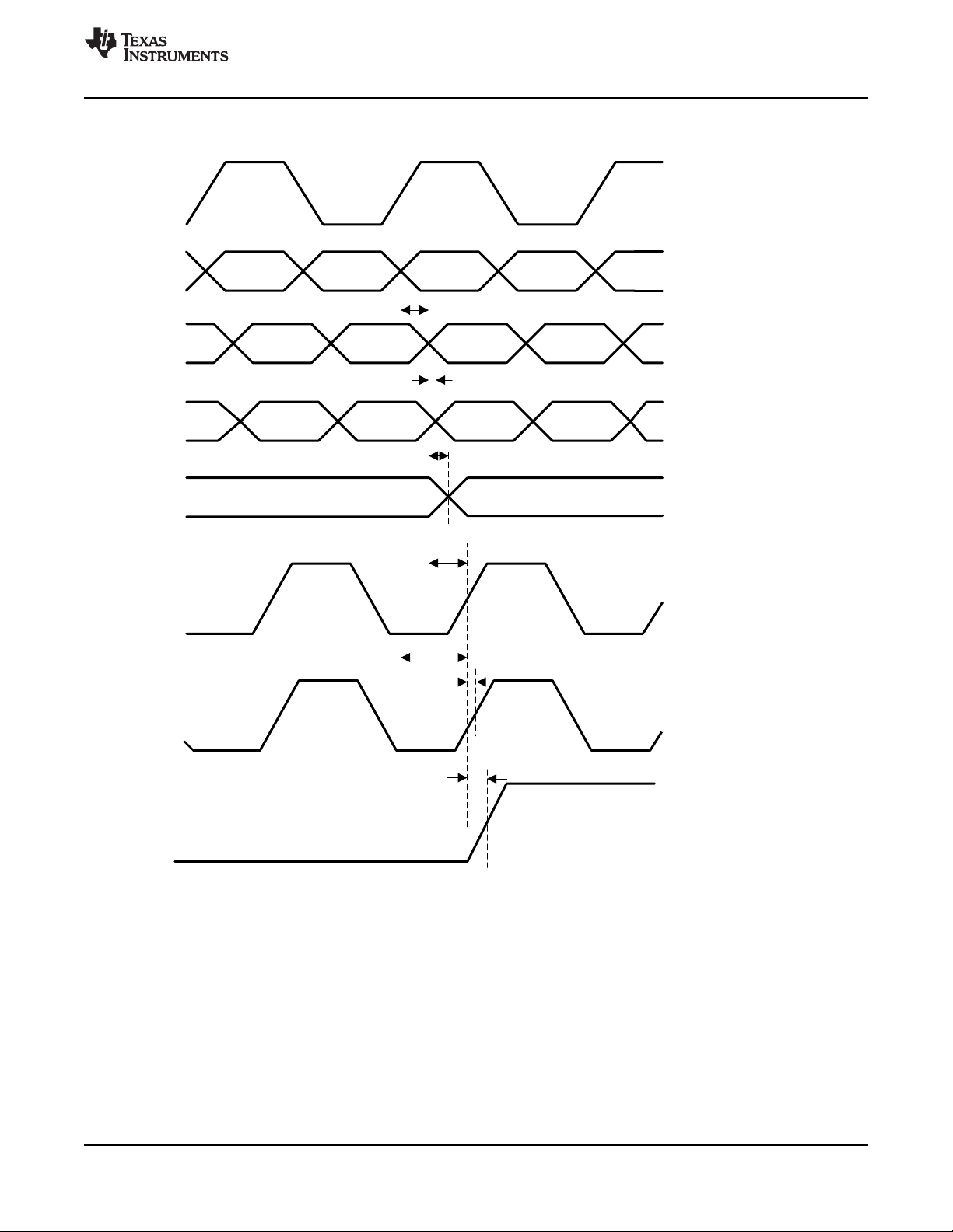
SCL
SCS
SDO
t
4
t
5
t
2
t
3
t
7
t
6
t
1
SDI
t
8
A31 D0D1
D15 D1 D0
A30
'21¶7&$5(
'21¶7&$5(
tri-state
CDCM6208V1F
SCAS943 –MAY 2015
www.ti.com
8.22 I2C TIMING
(1)
PARAMETER STANDARD MODE FAST MODE UNIT
MIN MAX MIN MAX
f
SCL
t
su(START)
t
h(START)
t
w(SCLL)
t
w(SCLH)
t
h(SDA)
t
su(SDA)
t
r-in
t
f-in
t
f-out
t
su(STOP)
t
BUS
t
glitch_filter
SCL Clock Frequency 0 100 0 400 kHz
START Setup Time (SCL high before SDA low) 4.7 0.6 μs
START Hold Time (SCL low after SDA low) 4.0 0.6 μs
SCL Low-pulse duration 4.7 1.3 μs
SCL High-pulse duration 4.0 0.6 μs
SDA Hold Time (SDA valid after SCL low) 0
(2)
3.45 0 0.9 μs
SDA Setup Time 250 100 ns
SCL / SDA input rise time 1000 300 ns
SCL / SDA input fall time 300 300 ns
SDA Output fall time from VIHmin to VILmax with a bus 250 250 ns
capacitance from 10 pF to 400 pF
STOP Setup Time 4.0 0.6 μs
Bus free time between a STOP and START condition 4.7 1.3 μs
Pulse width of spikes suppressed by the input glitch filter 75 300 75 300 ns
(1) For additional information, refer to the I2C-Bus specification, Version 2.1 (January 2000); the CDCM6208V1F meets the switching
characteristics for standard mode and fast mode transfer.
(2) The I2C master must internally provide a hold time of at least 300 ns for the SDA signal to bridge the undefined region of the falling edge
of SCL.
Figure 2. CDCM6208V1F SPI Port Timing
18 Submit Documentation Feedback Copyright © 2015, Texas Instruments Incorporated
Product Folder Links: CDCM6208V1F
STOP
~
~
START
STOP
~
~
~
~
~
~
~
~
t
BUS
t
SU(START)
SDA
SCL
t
h(START)
t
r(SM)
t
SU(SDATA)
t
W(SCLL)tW(SCLH)
t
h(SDATA)
t
r(SM)
t
f(SM)
t
f(SM)
t
SU(STOP)
V
IH(SM)
V
IL(SM)
V
IH(SM)
V
IL(SM)
ACK
www.ti.com
8.23 SPI Timing Requirements
PARAMETER MIN NOM MAX UNIT
f
Clock Frequency for the SCL 20 MHz
Clock
t
SPI_LE to SCL setup time 10 ns
1
t
SDI to SCL setup time 10 ns
2
t
SDO to SCL hold time 10 ns
3
t
SCL high duration 25 ns
4
t
SCL low duration 25 ns
5
t
SCL to SCS Setup time 10 ns
6
t
SCS Pulse Width 20 ns
7
t
SDI to SCL Data Valid (First Valid Bit after SCS) 10 ns
8
CDCM6208V1F
SCAS943 –MAY 2015
Figure 3. I2C Timing Diagram
Copyright © 2015, Texas Instruments Incorporated Submit Documentation Feedback 19
Product Folder Links: CDCM6208V1F
Frequency (Hz)
Jitter
2.9 ps
-50
10M10K100 1000 100k 1M
9.2 ps
0.92 ps
-60
0.29 ps
-70
-100
-80
-90
0.092 ps
-65
-55
-75
-85
-95
PSRR (dBc)
Frequency (MHz)
Jitter
0 ps-pp
60 ps-pp
100 ps-pp
120 ps-pp
140 ps-pp
180 ps-pp
200 ps-pp
400220 280 380
160 ps-pp
80 ps-pp
20 ps-pp
40 ps-pp
200 240 260 300 320 340 360
MSB-9, (1/1024) typ
all zero, (0) typ
MSB, (1/2) typ
MSB-1, (1/4) typ
MSB-2, (1/8) typ
MSB-3, (1/16) typ
MSB-4, (1/32) typ
MSB-5, (1/54) typ
MSB-6, (1/128) typ
MSB-7, (1/256) typ
MSB-13, (1/16384) typ
0x50A33D (÷x.315) typ
LSB, (1/1048576) typ
0x828F5 (÷x.51) typ
0xBAE14 (÷x.73) typ
Frequency (MHz)
Jitter
0
60
100
120
140
180
200
400
160
80
20
40
200 250 300 350
all zero, (0) max
MSB-9, (1/1024) typ
MSB-9, (1/1024) max
MSB-4, (1/32) max
MSB-13, (1/16384) max
MSB-13, (1/16384) typ
LSB, (1/1048576) max
LSB, (1/1048576) typ
MSB, (1/2) max
MSB, (1/2) typ
CDCM6208V1F
SCAS943 –MAY 2015
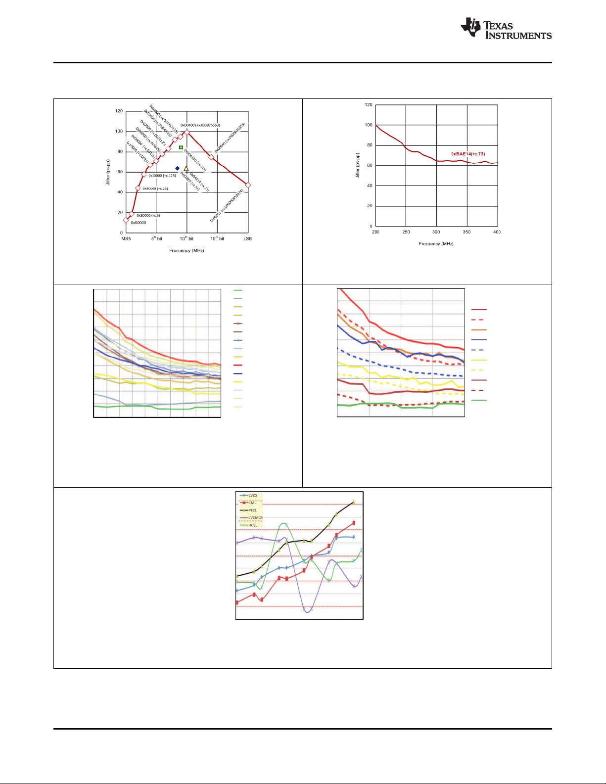
8.24 Typical Characteristics
www.ti.com
f
= 300 MHz
FRAC
Figure 4. Fractional Divider Bit Selection Impact on Jitter
Figure 6. Fractional Divider Bit Selection Impact on T
J
(Typical)
Using Divide by x.73 Example
Figure 5. Fractional Divider Input Frequency Impact on Jitter
Figure 7. Fractional Divider Bit Selection Impact on T
(Maximum Jitter Across Process, Voltage & Temperature)
J
20 Submit Documentation Feedback Copyright © 2015, Texas Instruments Incorporated
f
= 122 MHz
OUT
Figure 8. PSRR (in dBc and DJ [ps]) Over Frequency [Hz] and Output Signal Format
Product Folder Links: CDCM6208V1F

(spur/20)
-12
p-p
CLK
2 x 10
x fp
CDCM6208V1F
www.ti.com
SCAS943 –MAY 2015
8.24.1 Fractional Output Divider Jitter Performance
The fractional output divider jitter performance is a function of the fraction output divider input frequency as well
as actual fractional divide setting itself. To minimize the fractional output jitter, it is recommended to use the least
number of fractional bits and the highest input frequency possible into the divider. As observable in Figure 4, the
largest jitter contribution occurs when only one fractional divider bit is selected, and especially when the bits in
the middle range of the fractional divider are selected. Tested using a LeCroy 40 Gbps RealTime scope over a
time window of 200 ms. The RJimpact on TJis estimated for a BERT 10
(–12)
– 1. This measurement result is
overly pessimistic, as it does not bandwidth limit the high-frequencies. In a real system, the SERDES TX will BW
limit the jitter through its PLL roll-off above the TX PLL bandwidth of typically bit rate divided by 10.
8.24.2 Power Supply Ripple Rejection (PSRR) versus Ripple Frequency
See Figure 8 for reference.
Many system designs become increasingly more sensitive to power supply noise rejection. In order to simplify
design and cost, the CDCM6208V1F has built in internal voltage regulation, improving the power supply noise
rejection over designs with no regulators. As a result, the following output rejection is achieved:
The DJ due to PSRR can be estimated using Equation 1:
(1)
Example: Therefore, if 100 mV noise with a frequency of 10 kHz were observed at the output supply, the
according output jitter for a 122.88 MHz output signal with LVDS signaling could be estimated with DJ = 0.7ps.
Copyright © 2015, Texas Instruments Incorporated Submit Documentation Feedback 21
Product Folder Links: CDCM6208V1F
CDCM6208
LVCMOS
Phase Noise/
Spectrum
Analyzer
50
CDCM6208
LVCMOS
Oscilloscope
High impedance probe
1mA
CDCM6208
LVCMOS
Oscilloscope
High impedance probe
1mA
VDD_Yx
CDCM6208
LVCMOS
5pF
Oscilloscope
High impedance probe
CDCM6208V1F
SCAS943 –MAY 2015
9 Parameter Measurement Information
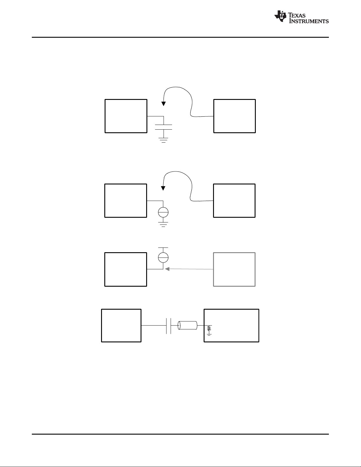
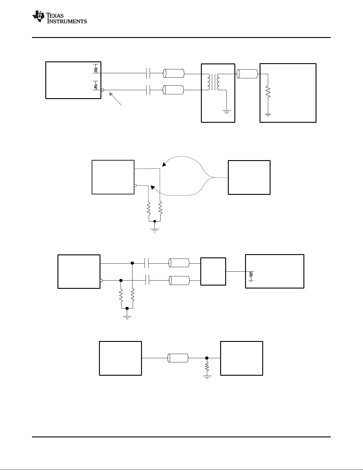
9.1 Characterization Test Setup
This section describes the characterization test setup of each block in the CDCM6208V1F.
www.ti.com
Figure 9. LVCMOS Output AC Configuration During Device Test (VOH, VOL, t
Figure 10. LVCMOS Output DC Configuration During Device Test
SLEW
)
22 Submit Documentation Feedback Copyright © 2015, Texas Instruments Incorporated
Figure 11. LVCMOS Output AC Configuration During Device Phase Noise Test
Product Folder Links: CDCM6208V1F
Signal
Generator
LVCMOS
CDCM6208
50
Offset = VDD_PRI/SEC/2
CDCM6208
HCSL
HCSL
50 50
Balun
Phase Noise/
Spectrum
Analyzer
50
CDCM6208
HCSL
HCSL
50
50
Oscilloscope
High impedance differential probe
Set to one of the following signaling
levels: LVPECL, CML, LVDS
CDCM6208
50 O
50
50
50 Balun
Phase Noise/
Spectrum
Analyzer
Y
N
Y
P
www.ti.com
Characterization Test Setup (continued)
Figure 12. LVDS, CML, and LVPECL Output AC Configuration During Device Test
CDCM6208V1F
SCAS943 –MAY 2015
Copyright © 2015, Texas Instruments Incorporated Submit Documentation Feedback 23
Figure 13. HCSL Output DC Configuration During Device Test
Figure 14. HCSL Output AC Configuration During Device Test
Figure 15. LVCMOS Input DC Configuration During Device Test
Product Folder Links: CDCM6208V1F
Signal
Generator
CDCM6208
Differential
100
100
VDD_PRI/SEC
100
100
Signal
Generator
LVPECL
LVPECL
50 50
CDCM6208
VDD_PRI/SEC - 2
Signal
Generator
LVDS
CDCM6208
LVDS
100
Signal
Generator
CML
CDCM6208
50
50
VDD_PRI/SEC
CML
CDCM6208V1F
SCAS943 –MAY 2015
Characterization Test Setup (continued)
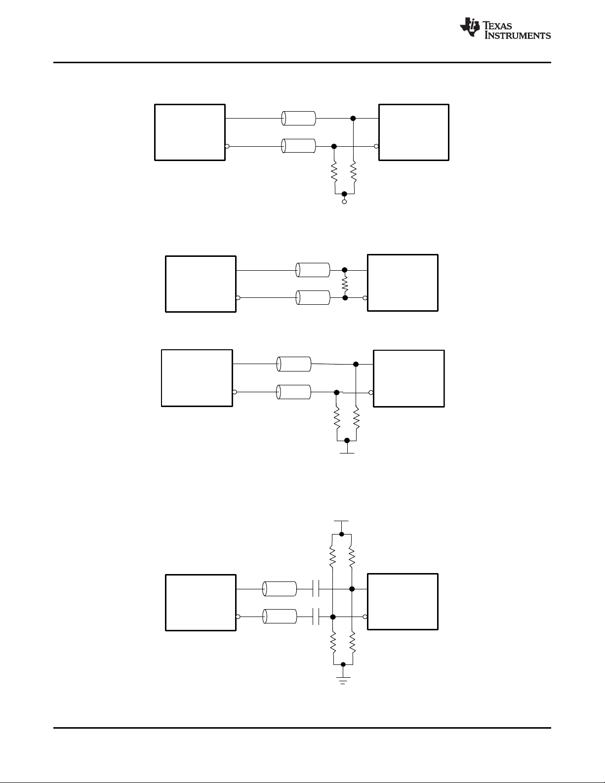
Figure 16. CML Input DC Configuration During Device Test
Figure 17. LVDS Input DC Configuration During Device Test
www.ti.com
Figure 18. LVPECL Input DC Configuration During Device Test
Figure 19. Differential Input AC Configuration During Device Test
24 Submit Documentation Feedback Copyright © 2015, Texas Instruments Incorporated
Product Folder Links: CDCM6208V1F
CDCM6208
Signal
Generator
Sine wave
Modulator
Reference
Input
Device Output
Power Supply
50 50
Balun
Phase Noise/
Spectrum
Analyzer
50
CDCM6208
Signal
Generator
Sine wave
Modulator
Reference
Input
Device Output
50 50
Balun
Phase Noise/
Spectrum
Analyzer
50
CDCM6208
www.ti.com
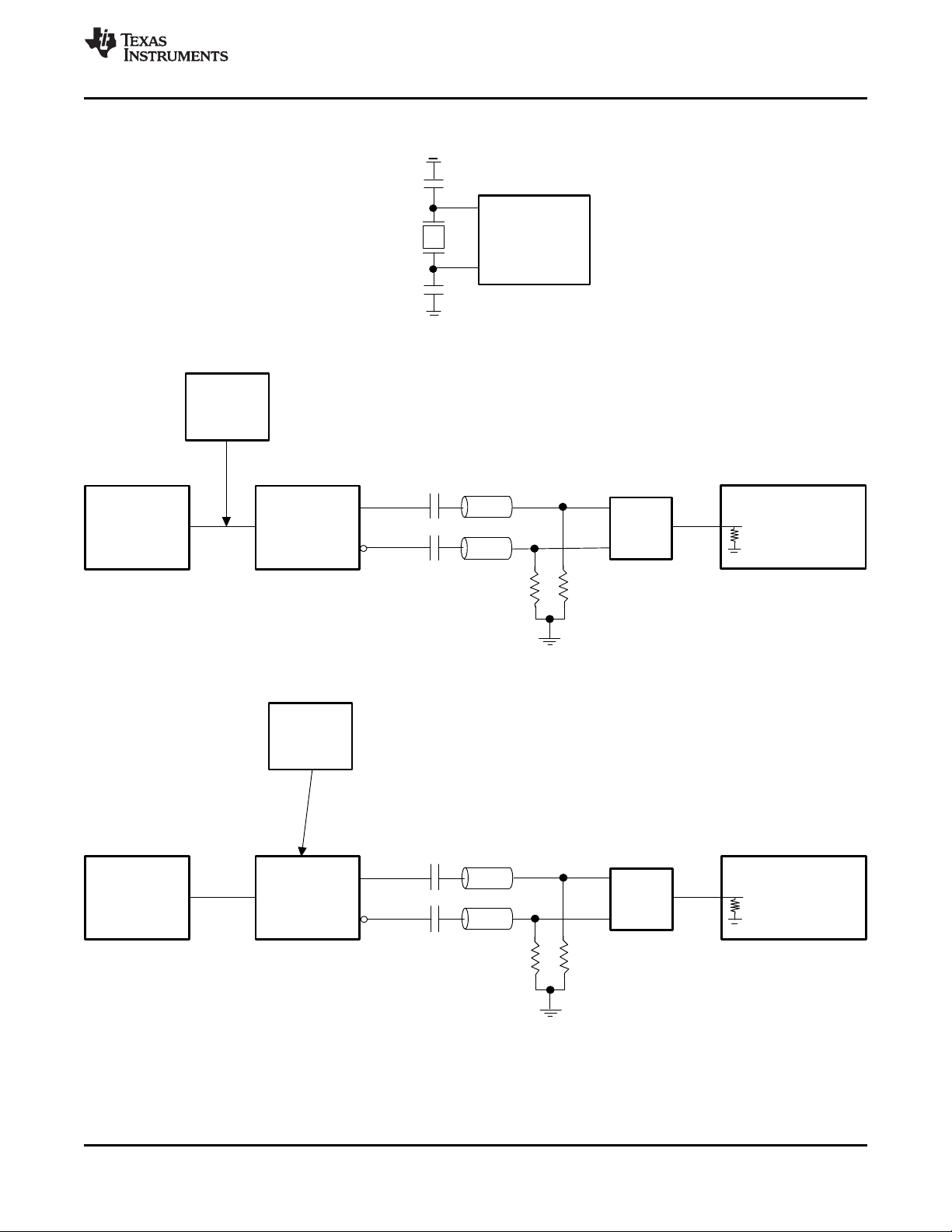
Characterization Test Setup (continued)
Figure 20. Crystal Reference Input Configuration During Device Test
CDCM6208V1F
SCAS943 –MAY 2015
Figure 21. Jitter transfer Test Setup
Copyright © 2015, Texas Instruments Incorporated Submit Documentation Feedback 25
Figure 22. PSNR Test Setup
Product Folder Links: CDCM6208V1F
V
OUT,SE
t
t
20%
80%
V
OD
Yx_N
V
OUT,DIFF,PP
= 2 x V
OD
0 V
20%
80%
t
R
t
F
CDCM6208V1F
SCAS943 –MAY 2015
Characterization Test Setup (continued)
Figure 23. Differential Output Voltage and Rise and Fall Time
www.ti.com
Figure 24. Single Ended Output Voltage and Rise and Fall Time
26 Submit Documentation Feedback Copyright © 2015, Texas Instruments Incorporated
Product Folder Links: CDCM6208V1F
VCXO_P
Yx_P
Yx_N
Yx_P
Yx_N
Yx_P
Yx_N
Yx_P/N
Yx_P/N
Differential
Differential, Integer Divide
Differential, Integer Divide
Differential, Fractional Divide
Single Ended, Integer Divide
Single Ended, Integer Divide
t
PD, SE
t
SK,SE,FRAC
t
PD,DIFF
t
SK,DIFF,INT
t
SK,DIFF,FRAC
Yx_P/N
t
SK,SE,INT
Single Ended, Fractional Divide
VCXO_P
Single Ended
t
SK,SE-DIFF,INT
www.ti.com
Characterization Test Setup (continued)
CDCM6208V1F
SCAS943 –MAY 2015
Figure 25. Differential and Single Ended Output Skew and Propagation Delay
Copyright © 2015, Texas Instruments Incorporated Submit Documentation Feedback 27
Product Folder Links: CDCM6208V1F

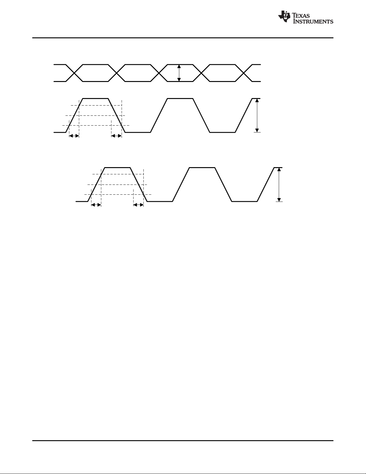
Control
Output
PLLInput
N
8-b,10-b
R
4-b
Host
Interface
Status/
Monitoring
Power
Conditioning
CDCM6208
Differential
XTAL
LVPECL/
CML/
LVDS
LVDS/
LVCMOS/
HCSL
Fractional Div
M
14-b
Integer Div
LVDS/
LVCMOS/
HCSL
VCO:
(2.39-2.55) GHz
Y0
Y1
Y2
Y3
Y4
Y5
Y6
Y7
PRI REF_
SEC REF_
Integer Div
PreScaler PS_A
÷4, ÷5, ÷6
ELF
REF_SEL
Smat MUX
Fractional Div
20-b
20-b
8-b
8-b
Fractional Div
20-b
Fractional Div
20-b
PreScaler PS_B
÷4, ÷5, ÷6
Φ
CDCM6208V1F
SCAS943 –MAY 2015
www.ti.com
10 Detailed Description
10.1 Overview
Supply Voltage: The CDCM6208V1F supply is internally regulated. Therefore each core and I/O supply can be
mixed and matched in any order according to the application needs. The device jitter performance is independent
of supply voltage.
Frequency Range: The PLL includes dual reference inputs with input multiplexer, charge pump, loop filter, and
VCO that operates from 2.39 GHz to 2.55 GHz.
Reference inputs: The primary and secondary reference inputs support differential and single ended signals from
8 kHz to 250 MHz. The secondary reference input also supports crystals from 10 MHz to 50 MHz. There is a 4bit reference divider available on the primary reference input. The input mux between the two references
supports simply switching or can be configured as Smart MUX and supports glitchless input switching.
Divider and Prescaler: In addition to the 4-bit input divider of the primary reference a 14-b input divider at the
output of input MUX and a cascaded 8-b and 10-b continuous feedback dividers are available. Two independent
prescaler dividers offer divide by /4, /5 and /6 options of the VCO frequency of which any combination can then
be chosen for a bank of 4 outputs (2 with fractional dividers and 2 that share an integer divider) through an
output MUX. A total of 2 output MUXes are available.
Phase Frequency Detector and Charge Pump: The PFD input frequency can range from 8 kHz to 100 MHz. The
charge pump gain is programmable and the loop filter consists of internal + partially external passive
components and supports bandwidths from a few Hz up to 400kHz.
10.2 Functional Block Diagram
28 Submit Documentation Feedback Copyright © 2015, Texas Instruments Incorporated
Figure 26. High-Level Block Diagram of CDCM6208V1F
Product Folder Links: CDCM6208V1F
CDCM6208V1F
www.ti.com
SCAS943 –MAY 2015
10.3 Feature Description
Phase Noise: The Phase Noise performance of the device can be summarized to:
Table 2. Synthesizer Mode (Loop filter BW >250 kHz)
RANDOM JITTER (ALL OUTPUTS) TOTAL JITTER
TYPICAL MAXIMUM MAXIMUM
10k-20MHz 12k-20MHz 10k-100MHz DJ-unbound DJ 10k-40MHz
0.27 ps-rms (Integer division) 50-220 ps-pp,
0.7ps-rms (fractional div) see
(1) Integrated Phase Noise (12kHz - 20 MHz) for 156.25 MHz output clock measured at room temperature using a 25 MHz Low Noise
reference source
(2) TJ= 20 psppapplies for LVPECL, CML, and LVDS signaling. TJlab characterization measured 8 pspp, (typical) and 12 pspp(max) over
PVT.
0.3 ps-rms (int div)
(1)
0.625 ps-rms (int div) 20 ps-pp
Table 3. Jitter Cleaner Mode (Loop filter BW < 1 kHz)
RANDOM JITTER (ALL OUTPUTS) TOTAL JITTER
TYPICAL MAXIMUM MAXIMUM
10k-20MHz 10k-20MHz 10k-100MHz DJ unbound DJ 10k-40MHz
1.6 ps-rms (Integer division) 70-240 ps-pp,
2.3 ps-rms (fractional div) 10k-20MHz see
2.1 ps-rms (int div) 2.14 ps-rms (int div) 40 ps-pp
Integer divider Fractional divider
RJ 10k-20MHz RJ 10k-20MHz
(2)
Integer divider Fractional divider
RJ 10k-20MHz RJ 10k-20MHz
Figure 4
Figure 4
Spurious Performance: The spurious performance is as follows:
• Less than -80 dBc spurious from PFD/reference clocks at 122.88 MHz output frequency in the Nyquist range.
• Less than -68 dBc spurious from output channel-to-channel coupling on the victim output at differential
signaling level operated at 122.88 MHz output frequency in the Nyquist range.
Device outputs:
The Device outputs offer multiple signaling formats: high-swing CML (LVPECL like), normal-swing CML (CML),
low-swing CML (LVDS like), HCSL, and LVCMOS signaling.
Table 4. Device Outputs
Outputs LVPECL CML LVDS HCSL LVCMOS OUTPUT DIVIDER
Y[3:0] X X X Integer only 1.55 - 800 MHz
Y[7:4] X X X
Integer 1.55 - 800 MHz
Fractional 1.00 - 400 MHz
FREQUENCY
RANGE
Outputs [Y0:Y3] are driven by 8-b continuous integer dividers per pair. Outputs [Y4:Y7] are each driven by 20-b
fractional dividers that can achieve any frequency with better than 1ppm frequency accuracy. The output skew is
typically less than 40 ps for differential outputs. The LVCMOS outputs support adjustable slew rate control to
control EMI. Pairs of 2 outputs can be operated at 1.8 V, 2.5 V or 3.3 V power supply voltage.
Device Configuration:32 distinct pin modes are available that cover many common use cases without the need
for any serial programming of the device. For maximum flexibility the device also supports SPI and I2C
programming. I2C offers 4 distinct addresses to support up to 4 devices on the same programming lines.
Copyright © 2015, Texas Instruments Incorporated Submit Documentation Feedback 29
Product Folder Links: CDCM6208V1F

10GbE
CDCM6208
Synthesizer
Mode
4x10G Ethernet ASIC
10G
PHY
10G
PHY
10G
PHY
10G
PHY
DDR1G
PHY
PCIe10G
PHY
DPLL
CDCM6208V1F
SCAS943 –MAY 2015
www.ti.com
Figure 27. Typical Use Case: CDCM6208V1F Example in Wireless Infrastructure Baseband Application
10.4 Device Functional Modes
10.4.1 Control Pins Definition
In the absence of a host interface, the CDCM6208V1F can be powered up in one of 32 pre-configured settings
when the pins are SI_MODE[1:0] = 10. The CDCM6208V1F has 5 control pins identified to achieve commonly
used networking frequencies, and change output types. The Smart Input MUX for the PLL is set in most
configurations to manual mode in pin mode. Based on the control pins settings for the on-chip PLL, the device
generates the appropriate frequencies and appropriate output signaling types at start-up. In the case of the PLL
loop filter, "JC" denotes PLL bandwidths of ≤ 1 kHz and "Synth" denotes PLL bandwidths of ≥ 100 kHz.
30 Submit Documentation Feedback Copyright © 2015, Texas Instruments Incorporated
Product Folder Links: CDCM6208V1F
www.ti.com
CDCM6208V1F
SCAS943 –MAY 2015
fout(Y4)
(1) (2)
Type(Y4)
fout(Y5)
Type(Y5)
fout(Y6)
Type(Y6)
12.000
66.666
33.333
fout(Y7)
1055
6667
3333
Table 5. Pre-Configured Settings of CDCM6208V1F Accessible by PIN[4:0]
pin[4:0]
SI_MODE[1:0]
0 I/O 25 Disable 25 Crystal 25 2500 125 PECL 125 PECL 125 PECL 125 PECL 25 HCSL 100 HCSL 100 Disable 100 Disable
1 I/O 25 Disable 25 Crystal 25 2500 125 PECL 125 PECL 125 PECL 125 PECL 25 HCSL 100 HCSL 100 Disable 100 Disable
Reserv
11
ed
10 0x00 1-V1F 25 25 Crystal 25 2500 156.25 LVDS 156.25 LVDS 156.25 LVDS 156.25 LVDS 156.25 LVDS 156.25 LVDS 156.25 LVDS 156.25 LVDS
10 0x01 2-V1F 25 25 Crystal 25 2500 125 LVDS 125 LVDS 125 LVDS 125 LVDS 25 LVDS 25 LVDS 25 LVDS 25 LVDS
10 0x02 3-V1F 25 25 Crystal 25 2500 156.25 LVDS 156.25 LVDS 156.25 LVDS 156.25 LVDS 25 LVDS 25 LVDS 25 25
10 0x03 4-V1F 25 25 Crystal 25 2500 125 LVDS 125 LVDS 125 LVDS 125 LVDS 156.25 LVDS 156.25 LVDS 25 LVDS 125
10 0x04 5-V1F 25 25 Crystal 25 2500 156.25 LVDS 156.25 LVDS 156.25 LVDS 156.25 LVDS 25 LVDS 25 LVDS 125 125
10 0x05 6-V1F 25 25 Crystal 25 2500 100 PECL 100 PECL 156.25 PECL 156.25 PECL 25 LVDS 100 HCSL 156.25 LVDS 156.25 LVDS
10 0x06 7-V1F 25 25 Crystal 25 2500 125 LVDS 125 LVDS 125 LVDS 125 LVDS 125 156.25 LVDS 156.25 LVDS 25 LVDS
10 0x07 8-V1F 25 25 Crystal 25 2500 156.25 PECL 156.25 PECL 25 PECL 25 PECL 125 156.25 LVDS 100 HCSL 100 HCSL
10 0x08 9-V1F 25 25 Crystal 25 2500 156.25 PECL 156.25 PECL 100 PECL 100 PECL 156.25 LVDS 156.25 LVDS 100 HCSL 100 HCSL
10 0x09 10-V1F 25 25 Crystal 25 2500 100 PECL 100 PECL 156.25 CML 156.25 CML 25 LVDS 100 HCSL 156.25 LVDS 156.25 LVDS
10 0x0A 11-V1F 25 25 Crystal 25 2500 100 PECL 100 PECL 100 PECL 100 PECL 25 125 50 000183
10 0x0B 12-V1F 25 25 Crystal 25 2400 25 PECL 25 PECL 100 CML 100 CML 25 25 100 HCSL 12
10 0x0C 13-V1F 25 25 Crystal 25 2500 156.25 PECL 156.25 PECL 125 PECL 125 PECL 25 25 25 LVDS 100 HCSL
10 0x0D 14-V1F 25 25 Crystal 25 2500 25 PECL 25 PECL 156.25 PECL 156.25 PECL 100 HCSL 100 HCSL 156.25 LVDS 666666
10 0x0E 15-V1F 25 25 Crystal 25 2500 125 LVDS 125 LVDS 125 LVDS 125 LVDS 25 LVDS 25 LVDS 25 LVDS 333333
Use Case
SPI MAN-
Default SEC
I2C MAN-
Default SEC
Type Type2 f(PFD) f(VCO)
fin(PRI_REF)
LVCM MAN-
OS SEC
LVCM MAN-
OS SEC
LVCM MAN- LVCM LVCM
OS SEC OS-PN OS-PN
LVCM MAN- LVCM
OS SEC OS-PN
LVCM MAN- LVCM LVCM
OS SEC OS-PN OS-PN
LVCM MAN-
OS SEC
LVCM MAN- LVCM
OS SEC OS-PN
LVCM MAN- LVCM
OS SEC OS-PN
LVCM MAN-
OS SEC
LVCM MAN-
OS SEC
LVCM MAN- LVCM LVCM LVCM LVCM
OS SEC OS-PN OS-PN OS-PN OS-PN
LVCM MAN- LVCM LVCM LVCM
OS SEC OS-PN OS-PN OS-PN
LVCM MAN- LVCM LVCM
OS SEC OS-PN OS-PN
LVCM MAN- LVCM
OS SEC OS-PN
LVCM MAN- LVCM
OS SEC OS-PN
fin(SEC_REF)
REF_SEL
fout(Y0)
TYPE(Y0)
fout(Y1)
Type(Y1)
fout(Y2)
Type(Y2)
fout(Y3)
Type(Y3)
Type(Y7)
(1) The functionality of the status 0 and status 1 pins in SPI and I2C mode is programmable.
(2) The REF_SEL input pin selects the primary or secondary input in MANUAL mode. That is: If the system only uses a XTAL on the secondary input, REF_SEL should be tied to VDD. The
primary and secondary input stage power supply must be always connected.
For all pin modes, STATUS0 outputs the PLL_LOCK signal and STATUS1 the LOSS OF REFERENCE.
General Note: in all pin mode, all voltage supplies must either be 1.8 V or 2.5/3.3 V and the PWR pin number 44 must be set to 0 or 1 accordingly. In SPI and I2C mode, the supply
voltages can be "mixed and matched" as long as the corresponding register bits reflect the supply voltage setting for each desired 1.8 V or 2.5/3.3 V supply. Exception: inputs configured
for LVDS signaling (Type = LVDS) are supply agnostic, and therefore can be powered from 2.5 V/3.3 V or 1.8 V regardless of the supply select setting of pin number 44.
Copyright © 2015, Texas Instruments Incorporated Submit Documentation Feedback 31
Product Folder Links: CDCM6208V1F
CDCM6208V1F
SCAS943 –MAY 2015
www.ti.com
Table 5. Pre-Configured Settings of CDCM6208V1F Accessible by PIN[4:0]
pin[4:0]
SI_MODE[1:0]
10 0x0F 16-V1F 25 25 Crystal 25 2500 156.25 LVDS 156.25 LVDS 100 PECL 100 PECL 25 25 LVDS 100 HCSL 100 HCSL
10 0x10 17-V1F 25 25 Crystal 25 2500 25 LVDS 25 LVDS 25 LVDS 25 LVDS 25 LVDS 156.25 LVDS 333333 333333
10 0x11 18-V1F 25 25 Crystal 25 2500 25 LVDS 25 LVDS 25 LVDS 25 PECL 25 LVDS 156.25 LVDS 156.25 LVDS 156.25 LVDS
10 0x12 19-V1F 25 25 Crystal 25 2500 100 CML 100 CML 100 CML 100 CML 100 HCSL 100 HCSL 100 HCSL 100 HCSL
10 0x13 20-V1F 25 25 Crystal 25 2500 156.25 PECL 156.25 PECL 125 PECL 125 PECL 156.25 HCSL 156.25 HCSL 100 HCSL 100 HCSL
10 0x14 21-V1F 25 25 Crystal 25 2400 100 LVDS 100 LVDS 100 LVDS 100 LVDS 24 100 LVDS 100 LVDS 333333
10 0x15 22-V1F 25 25 Crystal 25 2500 125 LVDS 125 LVDS 125 LVDS 125 LVDS 125 156.25 LVDS 156.25 LVDS 100
10 0x16 23-V1F 25 25 Crystal 25 2500 125 LVDS 125 LVDS 125 LVDS 125 LVDS 125 156.25 LVDS 100 LVDS 100
10 0x17 24-V1F 25 25 Crystal 25 2500 125 LVDS 125 LVDS 125 LVDS 125 LVDS 125 125 LVDS 156.25 LVDS 100
10 0x18 25-V1F 25 25 Crystal 25 2500 125 LVDS 125 LVDS 125 LVDS 125 LVDS 125 125 LVDS 100 LVDS 100
10 0x19 26-V1F 25 25 Crystal 25 2500 100 LVDS 100 LVDS 156.25 LVDS 156.25 LVDS 100 LVDS 100 HCSL 100 HCSL 100 HCSL
10 0x1A 27-V1F 25 25 Crystal 25 2500 100 LVDS 100 LVDS 156.25 LVDS 156.25 LVDS 100 LVDS 100 HCSL 156.25 LVDS 156.25 LVDS
10 0x1B 28-V1F 25 25 Crystal 25 2500 100 LVDS 100 LVDS 156.25 LVDS 156.25 LVDS 100 LVDS 100 HCSL 100 HCSL 156.25 LVDS
10 0x1C 29-V1F 25 25 Crystal 25 2500 100 LVDS 100 LVDS 100 LVDS 100 LVDS 999267 125 125 LVDS 333333
10 0x1D 30-V1F 25 25 Crystal 25 2500 100 LVDS 100 LVDS 100 LVDS 100 LVDS 999267 125 125 LVDS 100
10 0x1E 31-V1F 25 25 Crystal 25 2500 100 LVDS 100 LVDS 100 LVDS 100 LVDS 999267 125 125 LVDS 666666
10 0x1F 32-V1F 25 LVDS 25 Crystal 25 2500 156.25 LVDS 156.25 LVDS 100 LVDS 100 LVDS 125 LVDS 25 100 LVDS 100 LVDS
Use Case
Type Type2 f(PFD) f(VCO)
fin(PRI_REF)
LVCM MAN- LVCM
OS SEC OS-PN
LVCM MAN- LVCM LVCM
OS SEC OS-PN OS-PN
LVCM MAN-
OS SEC
LVCM MAN-
OS SEC
LVCM MAN-
OS SEC
LVCM MAN- LVCM LVCM
OS SEC OS-PN OS-PN
LVCM MAN- LVCM LVCM
OS SEC OS-PN OS-PN
LVCM MAN- LVCM LVCM
OS SEC OS-PN OS-PN
LVCM MAN- LVCM LVCM
OS SEC OS-PN OS-PN
LVCM MAN- LVCM LVCM
OS SEC OS-PN OS-PN
LVCM MAN-
OS SEC
LVCM MAN-
OS SEC
LVCM MAN-
OS SEC
LVCM MAN- LVCM LVCM LVCM
OS SEC OS-PN OS-PN OS-PN
LVCM MAN- LVCM LVCM LVCM
OS SEC OS-PN OS-PN OS-PN
LVCM MAN- LVCM LVCM LVCM
OS SEC OS-PN OS-PN OS-PN
fin(SEC_REF)
REF_SEL
MAN- LVCM
SEC OS-PN
fout(Y0)
TYPE(Y0)
fout(Y1)
Type(Y1)
fout(Y2)
Type(Y2)
fout(Y3)
(1) (2)
(continued)
fout(Y4)
Type(Y3)
23.999 83.333
5781 3333
23.999
5781
23.999 66.666
5781 6667
Type(Y4)
fout(Y5)
fout(Y6)
Type(Y5)
33.333 33.333
3333 3333
Type(Y6)
133.33
fout(Y7)
3333
Type(Y7)
32 Submit Documentation Feedback Copyright © 2015, Texas Instruments Incorporated
Product Folder Links: CDCM6208V1F

CDCM6208V1F
www.ti.com
SCAS943 –MAY 2015
10.4.2 Loop Filter Recommendations for Pin Modes
The following two tables provide the internal charge pump and R3/C3 settings for pin modes. The designer can
either design their own optimized loop filter, or use the suggested loop filter in the Table 6.
Table 6. CDCM6208V1F Loop Filter Recommendation for Pin Mode
PRI_REF SEC_REF
Use Case Loop Filter
pin [4:0]
SI_MODE[1:0]
0 I/O 25 Disable 25 Crystal 25 2.5m 100pF/500Ohm/22nF 242.5
1 I/O 25 Disable 25 Crystal 25 2.5m 100pF/500Ohm/22nF 242.5
Reserv
11
10 0x00 1-V1F 25 LVCMOS 25 Crystal 25 2.5m 100pF/500Ohm/22nF 242.5
10 0x01 2-V1F 25 LVCMOS 25 Crystal 25 2.5m 100pF/500Ohm/22nF 242.5
10 0x02 3-V1F 25 LVCMOS 25 Crystal 25 2.5m 100pF/500Ohm/22nF 242.5
10 0x03 4-V1F 25 LVCMOS 25 Crystal 25 2.5m 100pF/500Ohm/22nF 242.5
10 0x04 5-V1F 25 LVCMOS 25 Crystal 25 2.5m 100pF/500Ohm/22nF 242.5
10 0x05 6-V1F 25 LVCMOS 25 Crystal 25 2.5m 100pF/500Ohm/22nF 242.5
10 0x06 7-V1F 25 LVCMOS 25 Crystal 25 2.5m 100pF/500Ohm/22nF 242.5
10 0x07 8-V1F 25 LVCMOS 25 Crystal 25 2.5m 100pF/500Ohm/22nF 242.5
10 0x08 9-V1F 25 LVCMOS 25 Crystal 25 2.5m 100pF/500Ohm/22nF 337.5
10 0x09 10-V1F 25 LVCMOS 25 Crystal 25 2.5m 100pF/500Ohm/22nF 242.5
10 0x0A 11-V1F 25 LVCMOS 25 Crystal 25 2.5m 100pF/500Ohm/22nF 242.5
10 0x0B 12-V1F 25 LVCMOS 25 Crystal 25 2.5m 100pF/500Ohm/22nF 242.5
10 0x0C 13-V1F 25 LVCMOS 25 Crystal 25 2.5m 100pF/500Ohm/22nF 242.5
10 0x0D 14-V1F 25 LVCMOS 25 Crystal 25 2.5m 100pF/500Ohm/22nF 242.5
10 0x0E 15-V1F 25 LVCMOS 25 Crystal 25 2.5m 100pF/500Ohm/22nF 242.5
10 0x0F 16-V1F 25 LVCMOS 25 Crystal 25 2.5m 100pF/500Ohm/22nF 242.5
10 0x10 17-V1F 25 LVCMOS 25 Crystal 25 2.5m 100pF/500Ohm/22nF 242.5
10 0x11 18-V1F 25 LVCMOS 25 Crystal 25 2.5m 100pF/500Ohm/22nF 242.5
10 0x12 19-V1F 25 LVCMOS 25 Crystal 25 2.5m 100pF/500Ohm/22nF 242.5
10 0x13 20-V1F 25 LVCMOS 25 Crystal 25 2.5m 100pF/500Ohm/22nF 242.5
10 0x14 21-V1F 25 LVCMOS 25 Crystal 25 2.5m 100pF/500Ohm/22nF 242.5
10 0x15 22-V1F 25 LVCMOS 25 Crystal 25 2.5m 100pF/500Ohm/22nF 242.5
10 0x16 23-V1F 25 LVCMOS 25 Crystal 25 2.5m 100pF/500Ohm/22nF 242.5
ed
SPI MAN- 100
Default SEC Ohm
I2C MAN- 100
Default SEC Ohm
Freq Freq R3 C3
(MHz) (MHz) (Ohm) (pF)
Type Type
MAN- 100
SEC Ohm
MAN- 100
SEC Ohm
MAN- 100
SEC Ohm
MAN- 100
SEC Ohm
MAN- 100
SEC Ohm
MAN- 100
SEC Ohm
MAN- 100
SEC Ohm
MAN- 100
SEC Ohm
MAN- 100
SEC Ohm
MAN- 100
SEC Ohm
MAN- 100
SEC Ohm
MAN- 100
SEC Ohm
MAN- 100
SEC Ohm
MAN- 100
SEC Ohm
MAN- 100
SEC Ohm
MAN- 100
SEC Ohm
MAN- 100
SEC Ohm
MAN- 100
SEC Ohm
MAN- 100
SEC Ohm
MAN- 100
SEC Ohm
MAN- 100
SEC Ohm
MAN- 100
SEC Ohm
MAN- 100
SEC Ohm
f(PFD) ICP
(MHz) (mA)
REF_SEL
Recommended
C1/R2/C2
Internal LPF
Components
Copyright © 2015, Texas Instruments Incorporated Submit Documentation Feedback 33
Product Folder Links: CDCM6208V1F
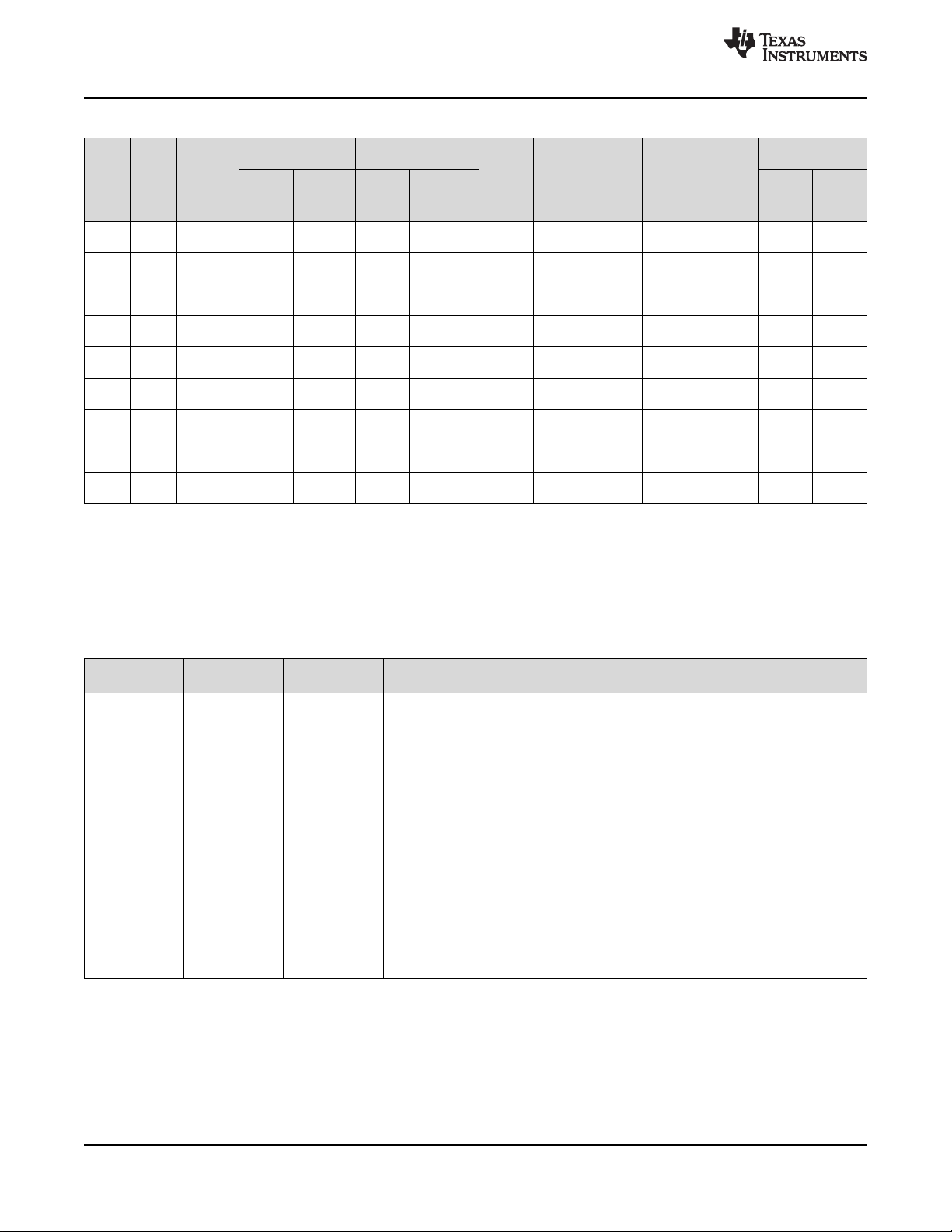
CDCM6208V1F
SCAS943 –MAY 2015
www.ti.com
Table 6. CDCM6208V1F Loop Filter Recommendation for Pin Mode (continued)
PRI_REF SEC_REF
Use Case Loop Filter
pin [4:0]
SI_MODE[1:0]
10 0x17 24-V1F 25 LVCMOS 25 Crystal 25 2.5m 100pF/500Ohm/22nF 242.5
10 0x18 25-V1F 25 LVCMOS 25 Crystal 25 2.5m 100pF/500Ohm/22nF 242.5
10 0x19 26-V1F 25 LVCMOS 25 Crystal 25 2.5m 100pF/500Ohm/22nF 242.5
10 0x1A 27-V1F 25 LVCMOS 25 Crystal 25 2.5m 100pF/500Ohm/22nF 242.5
10 0x1B 28-V1F 25 LVCMOS 25 Crystal 25 2.5m 100pF/500Ohm/22nF 242.5
10 0x1C 29-V1F 25 LVCMOS 25 Crystal 25 2.5m 100pF/500Ohm/22nF 242.5
10 0x1D 30-V1F 25 LVCMOS 25 Crystal 25 2.5m 100pF/500Ohm/22nF 242.5
10 0x1E 31-V1F 25 LVCMOS 25 Crystal 25 2.5m 100pF/500Ohm/22nF 242.5
10 0x1F 32-V1F 25 LVDS 25 Crystal 25 2.5m 100pF/500Ohm/22nF 242.5
Freq Freq R3 C3
(MHz) (MHz) (Ohm) (pF)
Type Type
MAN- 100
SEC Ohm
MAN- 100
SEC Ohm
MAN- 100
SEC Ohm
MAN- 100
SEC Ohm
MAN- 100
SEC Ohm
MAN- 100
SEC Ohm
MAN- 100
SEC Ohm
MAN- 100
SEC Ohm
MAN- 100
SEC Ohm
f(PFD) ICP
(MHz) (mA)
REF_SEL
Recommended
C1/R2/C2
Internal LPF
Components
10.4.3 Status Pins Definition
The device vitals such as input signal quality, smart mux input selection, and PLL lock can be monitored by
reading device registers or at the status pins STATUS1, and STATUS0. Register 3[12:7] allows for customization
of which vitals are mapped to these two pins. Table 7 lists the three events that can be mapped to each status
pin and which can also be read in the register space.
Table 7. CDCM6208V1F Status Pin Definition List
STATUS REGISTER BIT
SIGNAL NAME NO.
SEL_REF LVCMOS STATUS0, 1 Reg 3.12 Indicates Reference Selected for PLL:
LOS_REF LVCMOS STATUS0, 1 Reg 3.11 Loss of selected reference input observed at active input:
PLL_UNLOCK LVCMOS STATUS0, 1 Reg 3.10 Indicates unlock status for PLL (digital):
(1) The reverse logic between the register Q21.2 and the external output signal on STATUS0 or STATUS1.
SIGNAL TYPE SIGNAL NAME DESCRIPTION
Reg 3.9 0 → Primary input selected to drive PLL
1 → Secondary input selected to drive PLL
Reg 3.8 0 → Reference input present
1 → Loss of reference input
Important Note 1: For LOS_REF to operate properly, the secondary
input SEC_IN must be enabled. Set register Q4.5=1. If register
Q4.5 is set to zero, LOS_REF will output a static high signal
regardless of the actual input signal status on PRI_IN.
Reg 3.7 PLL locked → Q21.02 = 0 and V
PLL unlocked → Q21.2 = 1 and V
Note 2: I f the smartmux is enabled and both reference clocks stall,
STATUS0/1
STATUS0/1
the STATUSx output signal will 98% of the time indicate the LOS
condition with a static high signal. However, in 2% of the cases, the
LOS detection engine erroneously stalls at a state where the
STATUSx output PLL lock indicator will signalize high for 511 out of
every 512 PFD clock cycles.
= V
IH
= VILSee note
(1)
34 Submit Documentation Feedback Copyright © 2015, Texas Instruments Incorporated
Product Folder Links: CDCM6208V1F

Device
Control
And
Status
STATUS0
STATUS1/PIN0
PDN
RESETN/PWR
SCL/PIN4
SDI/SDA/PIN1
SDO/AD0/PIN2
SCS/AD1/PIN3
SI_MODE0
15 14 13 12 11 10 9 8 7 6 5 4 3 2 1 0
Reg 0
15 14 13 12 11 10 9 8 7 6 5 4 3 2 1 0
Reg1
15 14 13 12 11 10 9 8 7 6 5 4 3 2 1 0
Reg2
15 14 13 12 11 10 9 8 7 6 5 4 3 2 1 0
Reg3
15 14 13 12 11 10 9 8 7 6 5 4 3 2 1 0
Reg 20
15 14 13 12 11 10 9 8 7 6 5 4 3 2 1 0
Reg 21
15 14 13 12 11 10 9 8 7 6 5 4 3 2 1 0
Reg 22
15 14 13 12 11 10 9 8 7 6 5 4 3 2 1 0
Reg 23
15 14 13 12 11 10 9 8 7 6 5 4 3 2 1 0
Reg30
15 14 13 12 11 10 9 8 7 6 5 4 3 2 1 0
Reg31
REGISTER SPACE
Device
Hardware
SPI/
I2C
Port
Status
Pins
SPI: SI_MODE[1:0]=00; I2C: SI_MODE[1:0]=01; Pin Mode: SI_MODE[1:0]=10
SI_MODE1
Comm
Select
User Space
TI only
space
CDCM6208V1F
www.ti.com
SCAS943 –MAY 2015
NOTE
It is recommended to assert only one out of the three register bits for each of the status
pins. For example, to monitor the PLL lock status on STATUS0 and the selected reference
clock sources on STATUS1 output, the device register settings would be Q3.12 = Q3.7 =
1 and Q3.11 = Q3.10 = Q3.9 = Q3.8 = 0. If a status pin is unused, it is recommended to
set the according 3 register bits to zero (e.g. Q3[12:9] = 0 for STATUS0 = 0). If more than
one bit is enabled for each STATUS signal, the function becomes OR'ed. For example, if
Q3.11 = Q3.10 = 1 and Q3.12 = 0, the STATUS0 output would be high either if the device
goes out of lock or the selected reference clock signal is lost.
10.4.4 PLL Lock Detect
The PLL lock detection circuit is a digital detection circuit which detects any frequency error, even a single cycle
slip. The PLL unlock is signalized when a certain number of cycle slips have been exceeded, at which point the
counter is reset. A frequency error of 2% will cause PLL unlock to stay low. A 0.5% frequency error shows up as
toggling the PLL lock output with roughly 50% duty cycle at roughly 1/1000thof the PFD update frequency to the
device. A frequency error of 1ppm would show up as rare toggling low for a duration of approximately 1000 PFD
update clock cycles. If the system plans using PLL lock to toggle a system reset, then consider adding an RC
filter on the PLL LOCK output (Status 1 or Status 0) to avoid rare cycle slips from triggering an entire system
reset.
10.4.5 Interface and Control
The host (DSP, Microcontroller, FPGA, etc) configures and monitors the CDCM6208V1F via the SPI or I2C port.
The host reads and writes to a collection of control/status bits called the register file. Typically, a hardware block
is controlled and monitored via a specific grouping of bits located within the register file. The host controls and
monitors certain device-wide critical parameters directly, via control/status pins. In the absence of a host, the
CDCM6208V1F can be configured to operate in pin mode where the control pins [PIN0-PIN4] can be set
appropriately to generate the necessary clock outputs out of the device.
Figure 28. CDCM6208V1F Interface and Control Block
Within this register space, there are certain bits that have read/write access. Other bits are read-only (an attempt
to write to a read only bit will not change the state of the bit).
Copyright © 2015, Texas Instruments Incorporated Submit Documentation Feedback 35
Product Folder Links: CDCM6208V1F

5 4 3 2
Reg05
(s)
Bit Number(s)
R05.2
CDCM6208V1F
SCAS943 –MAY 2015
10.4.5.1 Register File Reference Convention
Figure 29 shows the method this document employs to refer to an individual register bit or a grouping of register
bits. If a drawing or text references an individual bit, the format is to specify the register number first and the bit
number second. The CDCM6208V1F contains 21 registers that are 16 bits wide. The register addresses and the
bit positions both begin with the number zero (0). A period separates the register address and bit address. The
first bit in the register file is address 'R0.0' meaning that it is located in Register 0 and is bit position 0. The last
bit in the register file is address R31.15 referring to the 16thbit of register address 31 (the 32ndregister in the
device
Figure 29. CDCM6208V1F Register Reference Format
www.ti.com
36 Submit Documentation Feedback Copyright © 2015, Texas Instruments Incorporated
Product Folder Links: CDCM6208V1F

OSC
=
OUT
(O × PS_A)
f
f
SEC_REF
VCO
=
M
(N × PS_A)
f
f
PRI_REF
VCO
=
(M × R)
(N × PS_A)
f
f
D15D14D13D12D11D10D9D8D7D6D5D4D3D2D1D
0
0 0 0 0
R/W
A10A9A8A7A6A5A4A3A2A1A
0
Fixed (4 bits) Register Address (11 bits) Data Payload (16 bits)
1 2 3 4 5 6 7 8 9 10 11 12 13 14 15 16 17 18 19 20 21 22 23 24 25 26 27 28 29 30 31 32
Message Field Definition
Bit Definition
Order of Transmission
Examples: Read Register 4: 1|000 0|000 0000 0100| xxxx xxxx xxxx xxxx
Write 0xF0F1 to Register 5: 0
|000 0|000 0000 0101| 1111 0000 1111 0001
MSB
LSB
CDCM6208V1F
www.ti.com
SCAS943 –MAY 2015
10.4.5.2 SPI - Serial Peripheral Interface
To enable the SPI port, tie the communication select pins SI_MODE[1:0] to ground. SPI is a master/slave
protocol in which the host system is always the master; therefore, the host always initiates communication
to/from the device. The SPI interface consists of four signal pins. The device SPI address is 0000.
Table 8. Serial Port Signals in SPI Mode
PIN
NAME NUMBER
SDI/SDA/PIN1 2 Input SDI: SPI Serial Data Input
SDO/AD0/PIN2 3 Output SDO: SPI Serial Data
SCS/AD1/PIN3 4 Input SCS: SPI Latch Enable
SCL/PIN4 5 Input SCL: SPI/I2C Clock
I/O DESCRIPTION
The host must present data to the device MSB first. A message includes a transfer direction bit, an address field,
and a data field as depicted in Figure 30
Figure 30. CDCM6208V1F SPI Message Format
10.4.5.2.1 Configuring the PLL
The CDCM6208V1F allows configuring the PLL to accommodate various input and output frequencies either
through an I2C or SPI programming interface or in the absence of programming, the PLL can be configured
through control pins. The PLL can be configured by setting the Smart Input MUX, Reference Divider, PLL Loop
Filter, Feedback Divider, Prescaler Divider, and Output Dividers.
For the PLL to operate in closed loop mode, the following condition in Equation 2 has to be met when using
primary input for the reference clock, and the condition in Equation 3 has to be met when using secondary input
for the reference clock.
(2)
(3)
In Equation 2 and Equation 3, ƒ
PRI_REF
is the reference input frequency on the primary input and ƒ
SEC_REF
is the
reference input frequency on the secondary input, R is the reference divider, M is the input divider, N is the
feedback divider, and PS_A the prescaler divider A.
The output frequency, ƒ
, is a function of ƒ
OUT
, the prescaler A, and the output divider (O), and is given by
VCO
Equation 4. (Use PS_B in for outputs 2, 3, 6, and 7).
(4)
Copyright © 2015, Texas Instruments Incorporated Submit Documentation Feedback 37
Product Folder Links: CDCM6208V1F

CDCM6208V1F
SCAS943 –MAY 2015
www.ti.com
When the output frequency plan calls for the use of some output dividers as fractional values, the following steps
are needed to calculate the closest achievable frequencies for those using fractional output dividers and the
frequency errors (difference between the desired frequency and the closest achievable frequency).
• Based on system needs, decide the frequencies that need to have best possible jitter performance.
• Once decided, these frequencies need to be placed on integer output dividers.
• Then a frequency plan for these frequencies with strict jitter requirements can be worked out using the
common divisor algorithm.
• Once the integer divider plans are worked out, the PLL settings (including VCO frequency, feedback divider,
input divider and prescaler divider) can be worked out to map the input frequency to the frequency out of the
prescaler divider.
• Then calculate the fractional divider values (whose values must be greater than 2) that are needed to support
the output frequencies that are not part of the common frequency plan from the common divisor algorithm
already worked out.
• For each fractional divider value, try to represent the fractional portion in a 20 bit binary scheme, where the
first fractional bit is represented as 0.5, the second fractional bit is represented as 0.25, third fractional bit is
represented as 0.125 and so on. Continue this process until the entire 20 bit fractional binary word is
exhausted.
• Once exhausted, the fraction can be calculated as a cumulative sum of the fractional bit x fractional value of
the fractional bit. Once this is done, the closest achievable output frequency can be calculated with the
mathematical function of the frequency out of the prescaler divider divided by the achievable fractional
divider.
• The frequency error can then be calculated as the difference between the desired frequency and the closest
achievable frequency.
10.5 Programming
10.5.1 Writing to the CDCM6208V1F
To initiate a SPI data transfer, the host asserts the SCS (serial chip select) pin low. The first rising edge of the
clock signal (SCL) transfers the bit presented on the SDI pin of the CDCM6208V1F. This bit signals if a read
(first bit high) or a write (first bit low) will transpire. The SPI port shifts data to the CDCM6208V1F with each
rising edge of SCL. Following the W/R bit are 4 fixed bits followed by 11 bits that specify the address of the
target register in the register file. The 16 bits that follow are the data payload. If the host sends an incomplete
message, (i.e. the host de-asserts the SCS pin high prior to a complete message transmission), then the
CDCM6208V1F aborts the transfer, and device makes no changes to the register file or the hardware. Figure 32
shows the format of a write transaction on the CDCM6208V1F SPI port. The host signals the CDCM6208V1F of
the completed transfer and disables the SPI port by de-asserting the SCS pin high.
38 Submit Documentation Feedback Copyright © 2015, Texas Instruments Incorporated
Product Folder Links: CDCM6208V1F

SCS
SCL
SCI
READ
SCI
SCO
HI-Z
16-BIT COMMAND 16-BIT DATA
'21¶7&$5(
A31 A30
A29 A28
A27
A26
A25
A24 A23
A22
A21
A20 A19
A18 A17
A16 D15
D14
D13
D12 D11
D10 D9 D8D7D6 D5 D4D3D2 D1 D0
D0
D1D2
D3
D4D5D6
D7
D8
D9
D10
D11
D12D13D14D15
A16A17
A18
A19
A20
A21
A22
A23
A24
A25
A26
A27
A28
A29A30
A31
CDCM6208
SDO
(#34)
Data out
SCS (#37)
LVCMOS
&
0
0
0
SDO internal
enable signal
CDCM6208V1F
www.ti.com
SCAS943 –MAY 2015
Programming (continued)
10.5.2 Reading from the CDCM6208V1F
As with the write operation, the host first initiates a SPI transfer by asserting the SCS pin low. The host signals a
read operation by shifting a logical high in the first bit position, signaling the CDCM6208V1F that the host is
imitating a read data transfer from the device. During the portion of the message in which the host specifies the
CDCM6208V1F register address, the host presents this information on the SDI pin of the device (for the first 15
clock cycles after the W/R bit). During the 16 clock cycles that follow, the CDCM6208V1F presents the data from
the register specified in the first half of the message on the SDO pin. The SDO output is 3-stated anytime SCS is
high, so that multiple SPI slave devices can be connected to the same serial bus. The host signals the
CDCM6208V1F that the transfer is complete by de-asserting the SCS pin high.
Figure 31.
10.5.3 Block Write/Read Operation
The device supports a block write and block read operation. The host need only specify the lowest address of the
sequence of addresses that the host needs to access. The CDCM6208V1F will automatically increment the
internal register address pointer if the SCS pin remains low after the SPI port finishes the initial 32-bit
transmission sequence. Each transmission of 16 bits (a data payload width) results in the device automatically
incrementing the address pointer (provided the SCS pin remains active low for all sequences).
Figure 32. CDCM6208V1F SPI Port Message Sequencing
10.5.4 I2C Serial Interface
With SI_MODE1=0 and SI_MODE0=1 the CDCM6208V1F enters I2C mode. The I2C port on the CDCM6208V1F
works as a slave device and supports both the 100 kHz standard mode and 400 kHz fast mode operations. Fast
mode imposes a glitch tolerance requirement on the control signals. Therefore, the input receivers ignore pulses
of less than 50 ns duration. The inputs of the device also incorporates a Schmitt trigger at the SDA and SCL
inputs to provide receiver input hysteresis for increased noise robustness.
NOTE
Communication through I2C is not possible while RESETN is held low.
Product Folder Links: CDCM6208V1F
Copyright © 2015, Texas Instruments Incorporated Submit Documentation Feedback 39

SDA
Data in
Data out
CDCM6208
CDCM6208V1F
SCAS943 –MAY 2015
www.ti.com
Programming (continued)
In an I2C bus system, the CDCM6208V1F acts as a slave device and is connected to the serial bus (data bus
SDA and clock bus SCL). The SDA port is bidirectional and uses an open drain driver to permit multiple devices
to be connected to the same serial bus. The CDCM6208V1F allows up to four unique CDCM6208V1F slave
devices to occupy the I2C bus in addition to any other I2C slave device with a different I2C address. These slave
devices are accessed via a 7-bit slave address transmitted as part of an I2C packet. Only the device with a
matching slave address responds to subsequent I2C commands. The device slave address is 10101xx (the two
LSBs are determined by the AD1 and AD0 pins). The five MSBs are hard-wired, while the two LSBs are set
through pins on device powerup.
During the data transfer through the I2C port interface, one clock pulse is generated for each data bit transferred.
The data on the SDA line must be stable during the high period of the clock. The high or low state of the data
line can change only when the clock signal on the SCL line is low. The start data transfer condition is
characterized by a high-to-low transition on the SDA line while SCL is high. The stop data transfer condition is
characterized by a low-to-high transition on the SDA line while SCL is high. The start and stop conditions are
always initiated by the master. Every byte on the SDA line must be eight bits long. Each byte must be followed
by an acknowledge bit and bytes are sent MSB first.
The acknowledge bit (A) or non-acknowledge bit (A) is the 9thbit attached to any 8-bit data byte and is always
generated by the receiver to inform the transmitter that the byte has been received (when A = 0) or not (when A
= 1). A = 0 is done by pulling the SDA line low during the 9thclock pulse and A = 1 is done by leaving the SDA
line high during the 9thclock pulse.
The I2C master initiates the data transfer by asserting a start condition which initiates a response from all slave
devices connected to the serial bus. Based on the 8-bit address byte sent by the master over the SDA line
(consisting of the 7-bit slave address (MSB first) and an R/W bit), the device whose address corresponds to the
transmitted address responds by sending an acknowledge bit. All other devices on the bus remain idle while the
selected device waits for data transfer with the master. The CDCM6208V1F slave address bytes are given in
below table.
After the data transfer has occurred, stop conditions are established. In write mode, the master asserts a stop
condition to end data transfer during the 10thclock pulse following the acknowledge bit for the last data byte from
the slave. In read mode, the master receives the last data byte from the slave but does not pull SDA low during
the 9thclock pulse. This is known as a non-acknowledge bit. By receiving the non-acknowledge bit, the slave
knows the data transfer is finished and enters the idle mode. The master then takes the data line low during the
low period before the 10thclock pulse, and high during the 10thclock pulse to assert a stop condition.
40 Submit Documentation Feedback Copyright © 2015, Texas Instruments Incorporated
Figure 33.
Product Folder Links: CDCM6208V1F
CDCM6208V1F
www.ti.com
SCAS943 –MAY 2015
Programming (continued)
For "Register Write/Read" operations, the I2C master can individually access addressed registers, that are made
of two 8-bit data bytes.
Table 9. I2C Slave Address Byte
A6 A5 A4 A3 A2 AD1 AD0 R/W
1 0 1 0 1 0 0 1/0
1 0 1 0 1 0 1 1/0
1 0 1 0 1 1 0 1/0
1 0 1 0 1 1 1 1/0
Table 10. Generic Programming Sequence
S Start Condition
Sr Repeated Condition
R/W 1 = Read (Rd) from slave; 0 = Write (Wr) to slave
A Acknowledge (ACK = 0 and NACK = 1)
P Stop Condition
Master to Slave Transmission
Slave to Master Transmission
Figure 34. Register Write Programming Sequence
1 7 1 1 8 1 8 1 8 1 8 1 1
SLAVE Register Register Data Data
S Wr A A A A A P
Address Address Address Byte Byte
Figure 35. Register Read Programming Sequence
1 7 1 1 8 1 8 1 1 1 1 1 8 1 8 1 1
SLAVE Register Register Slave Data Data
S Wr A A A S Rd A A A P
Address Address Address Address Byte Byte
Copyright © 2015, Texas Instruments Incorporated Submit Documentation Feedback 41
Product Folder Links: CDCM6208V1F

PRI
Y0
OUTMUX
INT
DIV
I
INMUX
SEC
R
N
M
Charge Pump
and
Loop Filter
Y1Y2Y3
Y6
Y7
INT
DIV
FRAC
DIV
FRAC
DIV
FRAC
DIV
FRAC
DIV
VCO
PSA
PSB
OUTMUX
PRI
SEC
PRI
SEC
REG 6
REG 8
REG 9,10,11
REG 15,16,17
REG 18,19, 20
REG 12,13,14
REG 0
REG 1
REG 2 / REG1
REG 3
REG 4
CDCM6208 Register programming
REG 9
REG 12
REG 4
REG 4
REG 5
REG 7
Y5 Y4
CDCM6208V1F
SCAS943 –MAY 2015
www.ti.com
10.6 Register Maps
In SPI/I2C mode the device can be configured through twenty registers. Register 4 configures the input, Reg 0-3
the PLL and dividers, and Register 5 - 20 configures the 8 different outputs.
Figure 36. Device Register Map
42 Submit Documentation Feedback Copyright © 2015, Texas Instruments Incorporated
Product Folder Links: CDCM6208V1F
www.ti.com
Register Maps (continued)
Table 11. Register 0
BIT BIT NAME RELATED BLOCK DESCRIPTION/FUNCTION
15:10 RESERVED These bits must be set to 0
PLL Internal Loop Filter Capacitor (C3) Selection
000 → 35 pF
001→ 112.5 pF
9:7 LF_C3[2:0] 011 → 242.5 pF
6:4 LF_R3[2:0] 011 → 100 Ω
3:1 PLL_ICP[2:0] PLL Charge Pump 011 → 2.0 mA
0 RESERVED
PLL Internal Loop Filter
(C3)
PLL Internal Loop Filter
(R3)
010 → 177.5 pF
100 → 310 pF
101 → 377.5 pF
110 → 445 pF
111 → 562.5 pF
PLL Internal Loop Filter Resistor (R3) Selection
000 → 10 Ω
001 → 30 Ω
010 → 60 Ω
100 → 530 Ω
101→ 1050 Ω
110 → 2080 Ω
111 → 4010 Ω
PLL Charge Pump Current Setting
000 → 500 µA
001 → 1.0 mA
010 → 1.5 mA
100 → 2.5 mA
101 → 3.0 mA
110 → 3.5 mA
111→ 4.0 mA
This bit is tied to zero statically, and it is recommended to set to 0
when writing to register.
CDCM6208V1F
SCAS943 –MAY 2015
Table 12. Register 1
BIT BIT NAME RELATED BLOCK DESCRIPTION/FUNCTION
15:2 PLL_REFDIV[13:0] PLL Reference Divider
1:0 PLL_FBDIV1[9:8] PLL Feedback Divider 1 PLL Feedback 10-b Divider Selection, Bits 9:8
PLL Reference 14-b Divider Selection
(Divider value is register value +1)
Table 13. Register 2
BIT BIT NAME RELATED BLOCK DESCRIPTION/FUNCTION
15:8 PLL_FBDIV1[7:0] PLL Feedback Divider 1
7:0 PLL_FBDIV0[7:0] PLL Feedback Divider 0
PLL Feedback 10-b Divider Selection, Bits 7:0
(Divider value is register value +1)
PLL Feedback 8-b Divider Selection
(Divider value is register value +1)
Copyright © 2015, Texas Instruments Incorporated Submit Documentation Feedback 43
Product Folder Links: CDCM6208V1F

CDCM6208V1F
SCAS943 –MAY 2015
Table 14. Register 3
BIT BIT NAME RELATED BLOCK DESCRIPTION/FUNCTION
15:13 RESERVED These bits must be set to 0
12 ST1_SEL_REFCLK 0 → Disable
11 ST1_LOR_EN 0 → Disable"
10 ST1_PLLLOCK_EN 0 → Disable
Device Status
9 ST0_SEL_REFCLK 0 → Disable
8 ST0_LOR_EN 0 → Disable
7 ST0_PLLLOCK_EN 0 → Disable
6 RSTN Device Reset 0 → Device In Reset (retains register values)
5 SYNCN Output Divider 0 → Forces synchronization
4 ENCAL PLL/VCO 0 → Disable
3:2 PS_B[1:0] PLL Prescaler Divider B
1:0 PS_A[1:0] PLL Prescaler Divider A
Reference clock status enable on Status 1 pin:
1 → Enable (See Table 7 for full description)
Loss-of-reference Enable on Status 1 pin:
1 → Enable (See Table 7 for full description)
PLL Lock Indication Enable on Status 1 pin:
1 → Enable (See Table 7 for full description)
Reference clock status enable on Status 0 pin:
1 → Enable (See Table 7 for full description)
Loss-of-reference Enable on Status 0 pin:
1 → Enable (See Table 7 for full description)
PLL Lock Indication Enable on Status 0 pin:"
1 → Enable (See Table 7 for full description)
Device Reset Selection:
1 → Normal Operation
Output Channel Dividers Synchronization Enable:
1 → Exits synchronization
PLL/VCO Calibration Enable:
1 → Enable
PLL Prescaler 1 Integer Divider Selection:
00 → Divide-by-4
01→ Divide-by-5
10 → Divide-by-6
11 → RESERVED
used for Y2, Y3, Y6, and Y7
PLL Prescaler 0 Integer Divider Selection:
00 → Divide-by-4
01 → Divide-by-5
10 → Divide-by-6
11 → RESERVED
used in PLL feedback, Y0, Y1, Y4, and Y5
www.ti.com
Table 15. Register 4
BIT BIT NAME RELATED BLOCK DESCRIPTION/FUNCTION
Smart MUX Pulse Width Selection. This bit controls the Smart MUX
delay and waveform reshaping.
15:14 SMUX_PW[1:0] in all pin modes)
Reference Input Smart
13 SMUX_MODE_SEL 1 → Manual select
12 SMUX_REF_SEL 1 → Secondary (only if REF_SEL pin is high)
44 Submit Documentation Feedback Copyright © 2015, Texas Instruments Incorporated
MUX
Product Folder Links: CDCM6208V1F
00 → PLL Smart MUX Clock Delay and Reshape Disabled (default
01 → PLL Smart MUX Clock Delay Enable
10 → PLL Smart MUX Clock Reshape Enable
11 → PLL Smart MUX Clock Delay and Reshape Enable
Smart MUX Mode Selection:
0 → Auto select
Note: in Auto select mode, both input buffers must be enabled. Set
R4.5 = 1 and R4.2 = 1
Smart MUX Selection for PLL Reference:
0 → Primary
This bit is ignored when smartmux is set to auto select (e.g. R4.13 =
0). See Table 7 for details.

CDCM6208V1F
www.ti.com
SCAS943 –MAY 2015
Table 15. Register 4 (continued)
BIT BIT NAME RELATED BLOCK DESCRIPTION/FUNCTION
11:8 CLK_PRI_DIV[3:0] Primary Input Divider 0000 → Divide by 1
7:6 SEC_SELBUF[1:0] 01 → LVDS
Secondary Input
5 EN_SEC_CLK 0 → Disable
4:3 PRI_SELBUF[1:0] 01→ LVDS
Primary Input
2 EN_PRI_CLK 0 → Disable
1 SEC_SUPPLY
0 PRI_SUPPLY
(1)
(2)
Secondary Input 0 → 1.8 V
Primary Input 0 → 1.8 V
(1) It is ok to power up the device with a 2.5 V/3.3 V supply while this bit is set to 0. To ensure best device performance this registers
should be updated after power-up to reflect the true VDD_SEC supply voltage used.
(2) It is ok to power up the device with a 2.5 V/3.3 V supply while this bit is set to 0. To ensure best device performance this registers
should be updated after power-up to reflect the true VDD_PRI supply voltage used.
Primary Input (R) Divider Selection:
1111 → Divide by 16
Secondary Input Buffer Type Selection:
00 → CML
10 → LVCMOS
11 → Crystal
Secondary input enable:
1 → Enable
Primary Input Buffer Type Selection:
00 → CML
10 → LVCMOS
11 → LVCMOS
Primary input enable:
1 → Enable
Supply voltage for secondary input:
1 → 2.5/3.3 V
Supply voltage for primary input:
1 → 2.5/3.3 V
Table 16. Register 5
BIT BIT NAME RELATED BLOCK DESCRIPTION/FUNCTION
15 RESERVED This bit must be set to 0
14 RESERVED This bit must be set to 0
13 RESERVED This bit must be set to 0
12 RESERVED This bit must be set to 0
11 RESERVED This bit must be set to 0
10 RESERVED This bit must be set to 0
9 RESERVED This bit must be set to 0
Output Channel 1 Type Selection:
8:7 SEL_DRVR_CH1[1:0]
Output Channel 1
6:5 EN _CH1[1:0] 01 → Enable
4:3 SEL_DRVR_CH0[1:0]
Output Channel 0
2:1 EN_CH0[1:0] 01 → Enable
00, 01 → LVDS
10 → CML
11 → PECL
Output channel 1 enable:
00 → Disable
10 → Drive static 0
11 → Drive static 1
Output Channel 0 Type Selection:
00, 01 → LVDS
10 → CML
11 → PECL
Output channel 0 enable:
00 → Disable
10 → Drive static 0
11 → Drive static 1
Copyright © 2015, Texas Instruments Incorporated Submit Documentation Feedback 45
Product Folder Links: CDCM6208V1F

CDCM6208V1F
SCAS943 –MAY 2015
Table 16. Register 5 (continued)
BIT BIT NAME RELATED BLOCK DESCRIPTION/FUNCTION
0 SUPPLY_CH0_1
(1) It is ok to power up the device with a 2.5 V/3.3 V supply while this bit is set to 0 and to update this bit thereafter.
(1)
Output Channels 0
and 1
Output Channels 0 and 1 Supply Voltage Selection:
0 → 1.8 V
1 → 2.5/3.3 V
Table 17. Register 6
BIT BIT NAME RELATED BLOCK DESCRIPTION/FUNCTION
15 RESERVED This bit must be set to 0
14 RESERVED This bit must be set to 0
13 RESERVED This bit must be set to 0
12 RESERVED This bit must be set to 0
11 RESERVED This bit must be set to 0
10 RESERVED This bit must be set to 0
9 RESERVED This bit must be set to 0
8 RESERVED This bit must be set to 0
7:0 OUTDIV0_1[7:0]
Output Channels 0 Output channels 0 and 1 8-b output integer divider setting
and 1 (Divider value is register value +1)
Table 18. Register 7
BIT BIT NAME RELATED BLOCK DESCRIPTION/FUNCTION
15 RESERVED This bit must be set to 0
14 RESERVED This bit must be set to 0
13 RESERVED This bit must be set to 0
12 RESERVED This bit must be set to 0
11 RESERVED This bit must be set to 0
10 RESERVED This bit must be set to 0
9 RESERVED This bit must be set to 0
Output Channel 3 Type Selection:
8:7 SEL_DRVR_CH3[1:0]
Output Channel 3
6:5 EN_CH3[1:0] 01 → Enable
4:3 SEL_DRVR_CH2[1:0]
Output Channel 2
2:1 EN_CH2[1:0] 01 → Enable
0 SUPPLY_CH2_3
(1) It is ok to power up the device with a 2.5 V/3.3 V supply while this bit is set to 0 and to update this bit thereafter.
(1)
Output Channels 2
and 3
00, 01 → LVDS
10 → CML
11 → PECL
Output channel 3 enable:
00 → Disable
10 → Drive static 0
11 → Drive static 1
Output Channel 2 Type Selection:
00, 01 → LVDS
10 → CML"
11 → PECL
Output channel 2 enable:
00 → Disable
10 → Drive static 0
11 → Drive static 1
Output Channels 2 and 3 Supply Voltage Selection:
0 → 1.8 V
1 → 2.5/3.3 V
www.ti.com
46 Submit Documentation Feedback Copyright © 2015, Texas Instruments Incorporated
Product Folder Links: CDCM6208V1F

www.ti.com
Table 19. Register 8
BIT BIT NAME RELATED BLOCK DESCRIPTION/FUNCTION
15 RESERVED This bit must be set to 0
14 RESERVED This bit must be set to 0
13 RESERVED This bit must be set to 0
12 RESERVED This bit must be set to 0
11 RESERVED This bit must be set to 0
10 RESERVED This bit must be set to 0
9 RESERVED This bit must be set to 0
8 RESERVED This bit must be set to 0
7:0 OUTDIV2_3[7:0]
Output Channels 2 Output channels 2 and 3 8-b output integer divider setting
and 3 (Divider value is register value +1)
Table 20. Register 9
BIT BIT NAME RELATED BLOCK DESCRIPTION/FUNCTION
15 RESERVED This bit must be set to 0
Output MUX setting for output channel 4:
14:13 OUTMUX_CH4[1:0]
12:10 PRE_DIV_CH4[2:0]
9 EN_FRACDIV_CH4 0 → Disable
8 LVCMOS_SLEW_CH4 0 → Normal
7 EN_LVCMOS_N_CH4
6 EN_LVCMOS_P_CH4 0 → Disable
5 RESERVED This bit must be set to 0
4:3 SEL_DRVR_CH4[2:0]
2:1 EN_CH4[1:0] 01 → Enable
0 SUPPLY_CH4
(1) It is ok to power up the device with a 2.5 V / 3.3 V supply while this bit is set to 0 and to update this bit thereafter.
(1)
Output Channel 4
00 and 11 → PLL
01 → Primary input
10 → Secondary input
Output channel 4 fractional divider's 3-b pre-divider setting (this predivider is bypassed if Q9.9 = 0)
000 → Divide by 2
001 → Divide by 3
111 → Divide by 1
All other combinations reserved
Output channel 4 fractional divider enable:
1 → Enable
Output channel 4 LVCMOS output slew:
1 → Slow
Output channel 4 negative-side LVCMOS enable:
0 → Disable
1 → Enable (Negative side can only be enabled if positive side is
enabled)
Output channel 4 positive-side LVCMOS enable:
1 → Enable
Output channel 4 type selection:
00 or 01 → LVDS
10 → LVCMOS
11 → HCSL
Output channel 4 enable:
00 → Disable
10 → Drive static 0
11 → Drive static 1
Output channel 4 Supply Voltage Selection:
0 → 1.8 V
1 → 2.5/3.3 V
CDCM6208V1F
SCAS943 –MAY 2015
Table 21. Register 10
BIT BIT NAME RELATED BLOCK DESCRIPTION/FUNCTION
15 RESERVED This bit must be set to 0
14 RESERVED This bit must be set to 0
Copyright © 2015, Texas Instruments Incorporated Submit Documentation Feedback 47
Product Folder Links: CDCM6208V1F
CDCM6208V1F
SCAS943 –MAY 2015
Table 21. Register 10 (continued)
BIT BIT NAME RELATED BLOCK DESCRIPTION/FUNCTION
13 RESERVED This bit must be set to 0
12 RESERVED This bit must be set to 0
11:4 OUTDIV4[7:0]
3:0 FRACDIV4[19:16] Output channel 4 20-b fractional divider setting, bits 19 - 16
Output Channel 4
Output channel 4 8-b integer divider setting
(Divider value is register value +1)
Table 22. Register 11
BIT BIT NAME RELATED BLOCK DESCRIPTION/FUNCTION
15:0 FRACDIV4[15:0] Output Channel 4 Output channel 4 20-b fractional divider setting, bits 15 - 0
Table 23. Register 12
BIT BIT NAME RELATED BLOCK DESCRIPTION/FUNCTION
15 RESERVED This bit must be set to 0
Output MUX setting for output channel 5:
14:13 OUTMUX_CH5[1:0]
12:10 PRE_DIV_CH5[2:0]
9 EN_FRACDIV_CH5 0 → Disable
8 LVCMOS_SLEW_CH5 0 → Normal
7 EN_LVCMOS_N_CH5
6 EN_LVCMOS_P_CH5 0 → Disable
5 RESERVED This bit must be set to 0
4:3 SEL_DRVR_CH5[2:0]
2:1 EN_CH5[1:0] 01 → Enable
0 SUPPLY_CH5
(1) It is ok to power up the device with a 2.5 V/3.3 V supply while this bit is set to 0 and to update this bit thereafter.
(1)
Output Channel 5
00 and 11 → PLL
01 → Primary input
10 → Secondary input
Output channel 5 fractional divider's 3-b pre-divider setting (this predivider is bypassed if Q12.9 = 0)
000 → Divide by 2
001 → Divide by 3
111 → Divide by 1
All other combinations reserved
Output channel 5 fractional divider enable:
1 → Enable
Output channel 5 LVCMOS output slew:
1 → Slow
Output channel 5 negative-side LVCMOS enable:
0 → Disable
1 → Enable (Negative side can only be enabled if positive side is
enabled)
Output channel 5 positive-side LVCMOS enable:
1 → Enable
Output channel 5 type selection:
00 or 01 → LVDS
10 → LVCMOS
11 → HCSL
Output channel 5 enable:
00 → Disable
10 → Drive static 0
11 → Drive static 1
Output channel 5Supply Voltage Selection:
0 → 1.8 V
1 → 2.5/3.3 V
www.ti.com
Table 24. Register 13
BIT BIT NAME RELATED BLOCK DESCRIPTION/FUNCTION
15 RESERVED This bit must be set to 0
14 RESERVED This bit must be set to 0
48 Submit Documentation Feedback Copyright © 2015, Texas Instruments Incorporated
Product Folder Links: CDCM6208V1F

www.ti.com
Table 24. Register 13 (continued)
BIT BIT NAME RELATED BLOCK DESCRIPTION/FUNCTION
13 RESERVED This bit must be set to 0
12 RESERVED This bit must be set to 0
11:4 OUTDIV5[7:0]
3:0 FRACDIV5[19:16] Output channel 5 20-b fractional divider setting, bits 19-16
Output Channel 5
Output channel 5 8-b integer divider setting
(Divider value is register value +1)
Table 25. Register 14
BIT BIT NAME RELATED BLOCK DESCRIPTION/FUNCTION
15:0 FRACDIV5[15:0] Output Channel 5 Output channel 5 20-b fractional divider setting, bits 15-0
Table 26. Register 15
BIT BIT NAME RELATED BLOCK DESCRIPTION/FUNCTION
15 RESERVED This bit must be set to 0
14 RESERVED This bit must be set to 0
13 RESERVED This bit must be set to 0
Output channel 6 fractional divider's 3-b pre-divider setting (this predivider is bypassed if Q15.9 = 0)
12:10 PRE_DIV_CH6[2:0]
9 EN_FRACDIV_CH6 0 → Disable
8 LVCMOS_SLEW_CH6 0 → Normal
7 EN_LVCMOS_N_CH6
Output Channel 6
6 EN_LVCMOS_P_CH6 0 → Disable
5 RESERVED This bit must be set to 0
4:3 SEL_DRVR_CH6[1:0]
2:1 EN_CH6[1:0] 01 → Enable
0 SUPPLY_CH6
(1) It is ok to power up the device with a 2.5 V/3.3 V supply while this bit is set to 0 and to update this bit thereafter.
(1)
000 → Divide by 2
001 → Divide by 3
111 → Divide by 1
All other combinations reserved
Output channel 6 fractional divider enable:
1 → Enable
Output channel 6 LVCMOS output slew:
1 → Slow
Output channel 6 negative-side LVCMOS enable:
0 → Disable
1 → Enable (Negative side can only be enabled if positive side is
enabled)
Output channel 6 positive-side LVCMOS enable:
1 → Enable
Output channel 6 type selection:
00 or 01 → LVDS
10 → LVCMOS
11 → HCSL
Output channel 6 enable:
00 → Disable
10 → Drive static 0
11 → Drive static 1
Output channel 6 Supply Voltage Selection:
0 → 1.8 V
1 → 2.5/3.3 V
CDCM6208V1F
SCAS943 –MAY 2015
Table 27. Register 16
BIT BIT NAME RELATED BLOCK DESCRIPTION/FUNCTION
15 RESERVED This bit must be set to 0
14 RESERVED This bit must be set to 0
13 RESERVED This bit must be set to 0
12 RESERVED This bit must be set to 0
Copyright © 2015, Texas Instruments Incorporated Submit Documentation Feedback 49
Product Folder Links: CDCM6208V1F

CDCM6208V1F
SCAS943 –MAY 2015
Table 27. Register 16 (continued)
BIT BIT NAME RELATED BLOCK DESCRIPTION/FUNCTION
11:4 OUTDIV6[7:0]
3:0 FRACDIV6[19:16] Output channel 6 20-b fractional divider setting, bits 19-16
Output Channel 6
Output channel 6 8-b integer divider setting
(Divider value is register value +1)
Table 28. Register 17
BIT BIT NAME RELATED BLOCK DESCRIPTION/FUNCTION
15:0 FRACDIV6[15:0] Output Channel 6 Output channel 6 20-b fractional divider setting, bits 15-0
Table 29. Register 18
BIT BIT NAME RELATED BLOCK DESCRIPTION/FUNCTION
15 RESERVED This bit must be set to 0
14 RESERVED This bit must be set to 0
13 RESERVED This bit must be set to 0
Output channel 7 fractional divider's 3-b pre-divider setting (this predivider is bypassed if Q18.9 = 0)
12:10 PRE_DIV_CH7[2:0]
9 EN_FRACDIV_CH7
8 LVCMOS_SLEW_CH7 Output channel 7 LVCMOS output slew: 0 → Normal, 1 → Slow
7 EN_LVCMOS_N_CH7 Enable (Negative side can only be enabled if positive side is
6 EN_LVCMOS_P_CH7
5 RESERVED This bit must be set to 0
4:3 SEL_DRVR_CH7[2:0]
2:1 EN_CH7[1:0]
0 SUPPLY_CH7
(1) It is ok to power up the device with a 2.5 V/3.3 V supply while this bit is set to 0 and to update this bit thereafter.
(1)
Output Channel 7
000 → Divide by 2
001 → Divide by 3
111 → Divide by 1
All other combinations reserved
Output channel 7 fractional divider enable: 0 → Disable, 1 →
Enable
Output channel 7 negative-side LVCMOS enable: 0 → Disable, 1 →
enabled)
Output channel 7 positive-side LVCMOS enable: 0 → Disable, 1 →
Enable
Output channel 7 type selection:00 or 01 → LVDS, 10 → LVCMOS,
11 → HCSL
Output channel 7 enable: 00 → Disable, 01 → Enable, 10 → Drive
static low, 11 → Drive static high
Output channel 7 Supply Voltage Selection: 0 → 1.8 V, 1 → 2.5/3.3
V
www.ti.com
Table 30. Register 19
BIT BIT NAME RELATED BLOCK DESCRIPTION/FUNCTION
15 RESERVED This bit must be set to 0
14 RESERVED This bit must be set to 0
13 RESERVED This bit must be set to 0
12 RESERVED This bit must be set to 0
11:4 OUTDIV7[7:0]
3:0 FRACDIV7[19:16] Output channel 7 20-b fractional divider setting, bits 19-16
Output Channel 7
Output channel 7 8-b integer divider setting
(Divider value is register value +1)
Table 31. Register 20
BIT BIT NAME RELATED BLOCK DESCRIPTION/FUNCTION
15:0 FRACDIV7[15:0] Output Channel 7 Output channel 7 20-b fractional divider setting, bits 15-0
50 Submit Documentation Feedback Copyright © 2015, Texas Instruments Incorporated
Product Folder Links: CDCM6208V1F

www.ti.com
Table 32. Register 21 (Read Only)
BIT BIT NAME RELATED BLOCK DESCRIPTION/FUNCTION
15 RESERVED This bit will read a 0
14 RESERVED This bit will read a 0
13 RESERVED This bit will read a 0
12 RESERVED This bit will read a 0
11 RESERVED This bit will read a 0
10 RESERVED This bit will read a 0
9 RESERVED This bit will read a 0
8 RESERVED This bit will read a 0
7 RESERVED This bit will read a 0
6 RESERVED This bit will read a 0
5 RESERVED This bit will read a 0
4 RESERVED This bit will read a 0
3 RESERVED This bit will read a 0
Indicates unlock status for PLL (digital):
0 → PLL locked
2 PLL_UNLOCK
Device Status
Monitoring
1 LOS_REF
0 SEL_REF 0 → Primary
1 → PLL unlocked
Note: the external output signal on Status 0 or Status 1 uses a
reversed logic, and indicates "lock" with a VOHsignal and unlock
with a VOLsignaling level.
Loss of reference input observed at input Smart MUX output in
observation window for PLL:
0 → Reference input present
1 → Loss of reference input
Indicates Reference Selected for PLL:
1 → Secondary
CDCM6208V1F
SCAS943 –MAY 2015
Table 33. Register 40 (Read Only)
BIT BIT NAME RELATED BLOCK DESCRIPTION/FUNCTION
15 RESERVED Ignore
14 RESERVED Ignore
13 RESERVED Ignore
12 RESERVED Ignore
11 RESERVED Ignore
10 RESERVED Ignore
9 RESERVED Ignore
8 RESERVED Ignore
7 RESERVED Ignore
6 RESERVED Ignore
5:3 VCO_VERSION
Device Information
2:0 DIE_REVISION 00X --> Engineering Prototypes
Indicates the device version (Read only):
000 → CDCM6208V1F
Indicates the silicon die revision (Read only):
010 --> Production Material
Copyright © 2015, Texas Instruments Incorporated Submit Documentation Feedback 51
Product Folder Links: CDCM6208V1F
CDCM6208V1F
SCAS943 –MAY 2015
www.ti.com
Table 34. Default Register Setting For SPI/I2C Modes
Register CDCM6208V1F
0 0x01B9
1 0x0000
2 0x0018
3 0x08F4
4 0x20B7
5 0x01BA
6 0x0003
7 0x0002
8 0x0003
9 0x0000
10 0x0040
11 0x0000
12 0x0000
13 0x0040
14 0x0000
15 0x0000
16 0x0040
17 0x0000
18 0x0002
19 0x0040
20 0x7940
. .
. .
. .
40 0x0001
52 Submit Documentation Feedback Copyright © 2015, Texas Instruments Incorporated
Product Folder Links: CDCM6208V1F

Pico Cell Clocking
DPLL
CDCM6208
APLL
GPS receiver
IEEE1588
timing extract
Ethernet
SyncE
Ethernet
Timing
Server
1pps
1pps
Core
Packet
network
FBADC
RXADC
TXDAC
RF LO
RF LO
CDCM6208
Synthesizer
Mode
TMS320TCI6616/18
DSP
AIF ALT
CORE
SRIO
PCIePacket
Accel
DR
Base Band DSP
Clocking
CDCM6208V1F
www.ti.com
SCAS943 –MAY 2015
11 Application and Implementation
NOTE
Information in the following applications sections is not part of the TI component
specification, and TI does not warrant its accuracy or completeness. TI’s customers are
responsible for determining suitability of components for their purposes. Customers should
validate and test their design implementation to confirm system functionality.
11.1 Application Information
The CDCM6208 is a highly integrated clock generator and jitter cleaner. The CDCM6208 derives its output
clocks from an on-chip oscillator which can be buffered through integer or fractional output dividers.
11.2 Typical Applications
Figure 37. Typical Application Circuit
Figure 38. Typical Application Circuit
11.2.1 Design Requirements
The most jitter sensitive application besides driving A-to-D converters are systems deploying a serial link using
Serializer and De-serializer implementation (for example, a 10 GigEthernet). Fully estimating the clock jitter
impact on the link budget requires an understanding of the transmit PLL bandwidth and the receiver CDR
bandwidth.
Copyright © 2015, Texas Instruments Incorporated Submit Documentation Feedback 53
Product Folder Links: CDCM6208V1F

CDCM6208V1F
SCAS943 –MAY 2015
www.ti.com
Typical Applications (continued)
11.2.1.1 Device Block-level Description
The CDCM6208V1F includes an on-chip PLL with an on-chip VCO. The PLL blocks consist of a universal input
interface, a phase frequency detector (PFD), charge pump, partially integrated loop filter, and a feedback divider.
Completing the CDCM6208V1F device are the combination of integer and fractional output dividers, and
universal output buffers. The PLL is powered by on-chip low dropout (LDO), linear voltage regulators and the
regulated supply network is partitioned such that the sensitive analog supplies are running from separate LDOs
than the digital supplies which use their own LDO. The LDOs provide isolation of the PLL from any noise in the
external power supply rail with a PSNR of better than -50 dB at all frequencies. The regulator capacitor pin
REG_CAP should be connected to ground by a 10 µF capacitor with low ESR (e.g. below 1 Ω ESR) to ensure
stability.
11.2.1.2 Device Configuration Control
Figure 40 illustrates the relationships between device states, the control pins, device initialization and
configuration, and device operational modes. In pin mode, the state of the control pins determines the
configuration of the device for all device states. In programming mode, the device registers are initialized to their
default state and the host can update the configuration by writing to the device registers. A system may transition
a device from pin mode to host connected mode by changing the state of the SI_MODE pins and then triggering
a device reset (either via the RESETN pin or via setting the RESETN bit in the device registers). In reset, the
device disables the outputs so that unwanted sporadic activity associated with device initialization does not
appear on the device outputs.
54 Submit Documentation Feedback Copyright © 2015, Texas Instruments Incorporated
Product Folder Links: CDCM6208V1F
(c) (PIN Mode)(b) (SPI/I2C Host Mode)
50k
#44 (RESET)
DVDD
CDCM6208
50k
#44 (RESET)
DVDD
CDCM6208
GPO
50k
#44 (PWR)
DVDD
CDCM6208
R
PD
if I/O power = 1.8V: RPD=0-Ohm
if I/O power=3.3V: RPD=open
(a)
(SPI/I2C Host mode)
5k
Host
Controller
www.ti.com
Typical Applications (continued)
11.2.1.3 Configuring the RESETN Pin
Figure 39 shows two typical applications examples of the RESETN pin.
Figure 39. RESETN/PWR Pin Configurations
CDCM6208V1F
SCAS943 –MAY 2015
Figure 39 (a) SPI / I2C mode only: shows the RESETN pin connected to a digital device that controls device
reset. The resistor and capacitor combination ensure reset is held low even if the CDCM6208V1F is powered up
before the host controller output signal is valid.
Figure 39 (b) SPI / I2C mode only:shows a configuration in which the user wishes to introduce a delay between
the time that the system applies power to the device and the device exiting reset. If the user does not use a
capacitor, then the device effectively ignores the state of the RESETN pin.
Figure 39 (c) Pin mode only: shows a configuration useful if the device is used in Pin Mode. Here device pin
number 44 becomes the PWR input. An external pull down resistor can be used to pull this pin down. If the
resistor is not installed, the pin is internally pulled high.
Copyright © 2015, Texas Instruments Incorporated Submit Documentation Feedback 55
Product Folder Links: CDCM6208V1F

PDN =1?
no
I2C Mode
(activate I2C IF)
SI_MODE1
SI_MODE0
10
01
00
SPI Mode
(activate SPI IF)
Pin Mode
latch PIN0 to PIN4, and
PWR
load device registers with defaults; registers
are customer programmable through serial IF
wait for selected reference
input signal (PRI/SEC) to
become valid
Configure all device settings
Calibrate VCO
Enter Pin Mode specified by
the PINx and PWR
PDN=1?
Normal device operation in
PIN mode
yes
PDN=1?
Normal device operation in
HOST mode
yes
wait for selected reference input
signal (PRI/SEC) to become valid
Calibrate VCO
Synchronize outputs
Enable all outputs
RESETN =1?
no
SYNCN=1?
no
Disable
all
outputs
Disable
all
outputs
SYNCN =1?
no
RESETN=1?
no
Disable
all
outputs
SYNCN=1?
no
Synchronize outputs
Enable outputs
SYNCN =1?
no
Disable
all
outputs
(all outputs are disabled)
Power on
Reset
RESETN =1?
no
CDCM6208V1F
SCAS943 –MAY 2015
www.ti.com
Typical Applications (continued)
Figure 40 shows how the different possible device configurations and when the VCO becomes calibrated and the
outputs turn on and off.
56 Submit Documentation Feedback Copyright © 2015, Texas Instruments Incorporated
Figure 40. Device Power up and Configuration
Product Folder Links: CDCM6208V1F

RESET=low
CDCM6208
Step 1
SPI or I2C
Master
GPO
Configure
Registers
0 to 21
CDCM6208
Step 2
SPI or I2C
Master
GPO
Release
RESET
50k
DVDD
RESET=high
50k
DVDD
outputs off
outputs on
SPI/I2C
SPI/I2C
Register
Space
Register
Space
CDCM6208V1F
www.ti.com
SCAS943 –MAY 2015
Typical Applications (continued)
11.2.1.4 Preventing False Output Frequencies in SPI/I2C Mode at Startup:
Some systems require a custom configuration and cannot tolerate any output to start up with a wrong frequency.
Holding RESET low at power-up until the device is fully configured keeps all outputs disabled. The device
calibrates automatically after RESET becomes released and starts out with the desired output frequency.
NOTE
The RESETN pin cannot be held low during I2C communication. Instead, use the SYNC
pin to disable the outputs during an I2C write operation, and toggle RESETN pin
afterwards. Alternatively, other options exist such as using the RESETN bit in the register
space to disable outputs until the write operation is complete.
Figure 41. Reset Pin Control During Register Loading
11.2.1.5 Power Down
When the PDN pin = 0, the device enters a complete power down mode with a current consumption of no more
than 1 mA from the entire device.
11.2.1.6 Device Power Up Timing:
Before the device outputs turn on after power up, the device goes through the following initialization routine:
Step 1: Power up ramp
Step 2: XO startup (if crystal is
used)
STEP DURATION COMMENTS
Depends on customer supply The POR monitor holds the device in power-down or reset until the
ramp time VDD supply voltage reaches 1.06 V (min) to 1.26 V (max)
Depends on XTAL. Could be This step assumes RESETN = 1 and PDN = 1.The XTAL startup
several ms; time is the time it takes for the XTAL to oscillate with sufficient
For NX3225GA 25 MHz typical amplitude. The CDCM6208V1F has a built-in amplitude detection
XTAL startup time measures 200 circuit, and holds the device in reset until the XTAL stage has
µs. sufficient swing.
Copyright © 2015, Texas Instruments Incorporated Submit Documentation Feedback 57
Table 35. Initialization Routine
Product Folder Links: CDCM6208V1F

1.05V
Outputs tristated
Step 2
XO startup
Step 3
Ref Clk Cntr
Step 4
FBCLK Cntr
Step 5
VCO CAL
Step 6: PLL lock time
Step 1: Pwr up
From here
on Device
is locked
Device outputs held static low (YxP=low, Yxn=high)
Y4 (HCSL)
Y4p
Y4n
1.8V
CDCM6208V1F
SCAS943 –MAY 2015
www.ti.com
Typical Applications (continued)
Table 35. Initialization Routine (continued)
STEP DURATION COMMENTS
This counter of 64 k clock cycles needs to expire before any further
Step 3: Ref Clock Counter the input to the PFD from PRI or SEC input has stabilized in
64k Reference clock cycles at
PFD input
64k FBCLK cycles with CW=32;
The duration is similar to Step 3, The Feedback counter delays the startup by another 64k PFD clock
Step 4: FBCLK counter
or can be more accurately cycles. This is so that all counters are well initialized and also ensure
estimated as: additional timing margin for the reference clock to settle. This step
Approximately 64k x PS_A x can range from 640 µs (f
N/2.48 GHz
Step 5: VCO calibration 128k PFD reference clock cycles takes exactly 128k PFD clock cycles. The duration can therefore
Step 6: PLL lock time approximately 3 x LBW synthesizer mode typically 10 µs). The initial output frequency will be
Step 7: PLL Lock indicator high will go high after approximately 2048 to 2560 PFD clock cycles to
approximately 2305 PFD clock
cycles
power-up step is done inside the device. This counter ensures that
frequency. The duration of this step can range from 640 µs (f
100 MHz) to 8 sec (8 kHz PFD).
= 100 MHz) to 8 sec (f
PFD
PFD
= 8kHz).
PFD
=
This step calibrates the VCO to the exact frequency range, and
range from 1280 µs (f
= 100 MHz) to 16 sec (f
PFD
= 8 KHz).
PFD
The Outputs turn on immediately after calibration. A small frequency
error remains for the duration of approximately 3 x LBW (so in
lower than the target output frequency, as the loop filter starts out
initially discharged.
The PLL lock indicator if selected on output STATUS0 or STATUS1
indicate PLL is now locked.
58 Submit Documentation Feedback Copyright © 2015, Texas Instruments Incorporated
Figure 42. Powerup Time
Product Folder Links: CDCM6208V1F
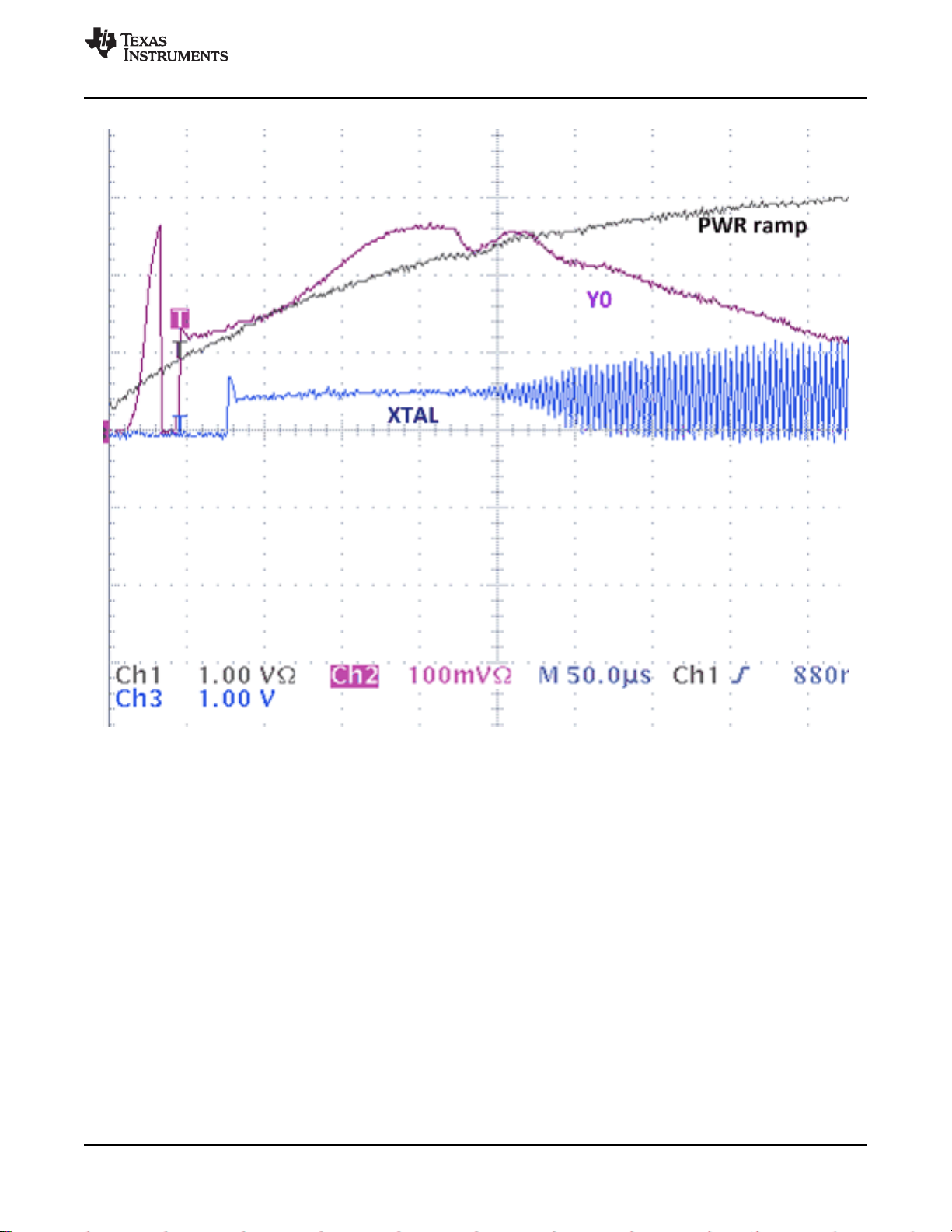
www.ti.com
CDCM6208V1F
SCAS943 –MAY 2015
Figure 43. XTAL Startup Using NX3225GA 25 MHz (Step 2)
Copyright © 2015, Texas Instruments Incorporated Submit Documentation Feedback 59
Product Folder Links: CDCM6208V1F

4=3.5%
250ns
140ns
Step 7
Time from PLL Lock
to LOCK signal asserting high on STATUS0 = 78s
CDCM6208V1F
SCAS943 –MAY 2015
www.ti.com
Figure 44. PLL Lock Behavior (Step 6)
11.2.1.7 Input Mux and Smart Input Mux
The Smart Input MUX supports auto-switching and manual-switching using control pin (and through register).
The Smart Input MUX is designed such that glitches created during switching in both auto and manual modes
are suppressed at the MUX output.
Table 36. Input Mux Selection
SI_MODE1 REGISTER 4 BIT 12 REF_SEL
PIN NO. 47 SMUX_REF_SEL PIN NO. 6
0 (SPI/I2C mode)
1 (pin mode) not available
Example 1:An application desired to auto-select the clock reference in SPI/I2C mode. During production testing
REGISTER 4 BIT
13SMUX_MODE_SE SELECTED INPUT
L
0 X X
0 Primary input
1
1 Secondary input
1
Auto Select Priority is given to Primary
Reference input.
1
0 Primary input
1 Secondary input
0 Primary or Auto (see Table 5)
1 Secondary or Auto (see Table 5)
input select through
SPI/I2C
input select through
external pin
however, the system needs to force the device to use the primary followed by the secondary input. The settings
would be as follows:
1. Tie REF_SEL pin always high
2. For primary clock input testing, use R4[13:12] = 10
3. For secondary clock input testing, set R4[13:12] = 11.
4. For the auto-mux setting in the final product shipment, set R3[13:12]=01 or 00
Example 2: The application wants to select the clock input manually without programming SPI/I2C. In this case,
program R4[13:12] = 11, and select primary or secondary input by toggling REF_SEL low or high.
60 Submit Documentation Feedback Copyright © 2015, Texas Instruments Incorporated
Product Folder Links: CDCM6208V1F

CDCM6208V1F
www.ti.com
SCAS943 –MAY 2015
SmartMux input frequency limitation: In the automatic mode, the frequencies of both inputs to the smart mux
(PRI_REF divided by R and SEC_REF) need to be similar; however, they can vary by up to 20%.
Switching behavior: The input clocks can have any phase. When switching happens between one input clock to
the other, the phase of the output clock slowly transitions to the phase of the newly selected input clock. There
will be no-phase jump at the output. The phase transition time to the new reference clock signal depends on the
PLL loop filter bandwidth. Auto-switch assigns higher priority to PRI_REF and lower priority to SEC_REF. The
timing diagram of an auto-switch at the input MUX is shown in Figure 45.
Figure 45. Smart Input MUX Auto-Switch Mode Timing Diagram
11.2.1.8 Universal INPUT Buffer (PRI_REF, SEC_REF)
The universal input buffers support multiple signaling formats (LVDS, CML or LVCMOS) and these require
external termination schemes. The secondary input buffer also supports crystal inputs and Table 28 provides the
characteristics of the crystal that can be used. Both inputs incorporate hysteresis.
11.2.1.9 VCO Calibration
The LC VCO is designed using high-Q monolithic inductors and has low phase noise characteristics. The VCO of
the CDCM6208V1F must be calibrated to ensure that the clock outputs deliver optimal phase noise performance.
Fundamentally, a VCO calibration establishes an optimal operating point within the tuning range of the VCO.
While transparent to the user, the CDCM6208V1F and the host system perform the following steps comprising a
VCO calibration sequence:
1. Normal Operation- When the CDCM6208V1F is in normal (operational) mode, the state of both the power
down pin (PDN) and reset pin (RESETN) is high.
2. Entering the reset state – If the user wishes to restore all device defaults and initiate a VCO calibration
sequence, then the host system must place the device in reset via the PDN pin, via the RESETN pin, or by
removing and restoring device power. Pulling either of these pins low places the device in the reset state.
Holding either pin low holds the device in reset.
3. Exiting the reset state – The device calibrates the VCO either by exiting the device reset state or through
the device reset command initiated via the host interface. Exiting the reset state occurs automatically after
power is applied and/or the system restores the state of the PDN or RESETN pins from the low to high state.
Exiting the reset state using this method causes the device defaults to be loaded/reloaded into the device
register bank. Invoking a device reset via the register bit does not restore device defaults; rather, the device
retains settings related to the current clock frequency plan. Using this method allows for a VCO calibration
for a frequency plan other than the default state (i.e. the device calibrates the VCO based on the settings
contained within the register bank at the time that the register bit is accessed). The nominal state of this bit is
low. Writing this bit to a high state and then returning it to the low state invokes a device reset without
restoring device defaults.
4. Device stabilization – After exiting the reset state as described in Step 3, the device monitors internal
voltages and starts a reset timer. Only after internal voltages are at the correct level and the reset time has
expired will the device initiate a VCO calibration. This ensures that the device power supplies and phase
locked loops have stabilized prior to calibrating the VCO.
5. VCO Calibration – The CDCM6208V1F calibrates the VCO. During the calibration routine, the device holds
Copyright © 2015, Texas Instruments Incorporated Submit Documentation Feedback 61
Product Folder Links: CDCM6208V1F

CDCM6208V1F
SCAS943 –MAY 2015
www.ti.com
all outputs in reset so that the CDCM6208V1F generates no spurious clock signals.
11.2.1.10 Reference Divider (R)
The reference (R) divider is a continuous 4-b counter (1 – 16) that is present on the primary input before the
Smart Input MUX. It is operational in the frequency range of 8 kHz to 250 MHz. The output of the R divider sets
the input frequency for the Smart MUX, and the auto switch capability of the Smart MUX can then be employed
as long as the secondary input frequency is no more than ± 20% different from the output of the R divider.
11.2.1.11 Input Divider (M)
The input (M) divider is a continuous 14-b counter (1 – 16384) that is present after the Smart Input MUX. It is
operational in the frequency range of 8 kHz to 250 MHz. The output of the M divider sets the PFD frequency to
the PLL and should be in the range of 8 kHz to 100 MHz.
11.2.1.12 Feedback Divider (N)
The feedback (N) divider is made up of cascaded 8-b counter divider (1 – 256) followed by a 10-b counter divider
(1 – 1024) that are present on the feedback path of the PLL. It is operational in the frequency range of 8 kHz to
800 MHz. The output of the N divider sets the PFD frequency to the PLL and should be in the range of 8 kHz to
100 MHz. The frequency out of the first divider is required to be less than or equal to 200 MHz to ensure proper
operation.
11.2.1.13 Prescaler Dividers (PS_A, PS_B)
The prescaler (PS) dividers are fed by the output of the VCO and are distributed to the output dividers (PS_A to
the dividers for Outputs 0, 1, 4, and 5 and PS_B to the dividers for Outputs 2, 3, 6, and 7. PS_A also completes
the PLL as it also drives the input of the Feedback Divider (N).
11.2.1.14 Phase Frequency Detector (PFD)
The PFD takes inputs from the Smart Input MUX output and the feedback divider output and produces an output
that is dependent on the phase and frequency difference between the two inputs. The allowable range of
frequencies at the inputs of the PFD is from 8 kHz to 100 MHz.
11.2.1.15 Charge Pump (CP)
The charge pump is controlled by the PFD which dictates either to pump up or down in order to charge or
discharge the integrating section of the on-chip loop filter. The integrated and filtered charge pump current is then
converted to a voltage that drives the control voltage node of the internal VCO through the loop filter. The range
of the charge pump current is from 500 µA to 4 mA.
11.2.1.16 Programmable Loop Filter
The on-chip PLL supports a partially internal and partially external loop filter configuration for all PLL loop
bandwidths where the passive external components C1, C2, and R2 are connected to the ELF pin as shown in
Figure 46 to achieve PLL loop bandwidths from 400 kHz down to 10 Hz.
62 Submit Documentation Feedback Copyright © 2015, Texas Instruments Incorporated
Product Folder Links: CDCM6208V1F

ELF
R2
C2
C1
R3
C3
CDCM6208V1F
www.ti.com
SCAS943 –MAY 2015
Figure 46. CDCM6208V1F PLL Loop Filter Topology
11.2.1.16.1 Loop Filter Component Selection
The loop filter setting and external resistor selection is important to set the PLL to best possible bandwidth and to
minimize jitter. A high bandwidth (≥ 100 kHz) provides best input signal tracking and is therefore desired with a
clean input reference (synthesizer mode). A low bandwidth (≤ 1 kHz) is desired if the input signal quality is
unknown (jitter cleaner mode). TI provides a software tool that makes it easy to select the right loop filter
components. C1, R2, and C2 are external loop filter components, connected to the ELF pin. The 3rdpole of the
loop filter is device internal with R3 and C3 register selectable.
11.2.1.16.2 Device Output Signaling
LVDS-like: All outputs Y[7:0] support LVDS-like signaling. The actual output stage uses a CML structure and
drives a signal swing identical to LVDS (~350mV). The output slew rate is faster than standard LVDS for best
jitter performance. The LVDS-like outputs should be AC-coupled when interfacing to a LVDS receiver. See
reference schematic Figure 64 for an example. The supply voltage for outputs configured LVDS can be selected
freely between 1.8 V and 3.3 V.
LVPECL-like: Outputs Y[3:0] support LVPECL-like signaling. The actual output stage uses a CML structure but
drives the same signal amplitude and rise time as true emitter coupled logic output stages. The LVPECL-like
outputs should be AC-coupled, and contrary to standard PECL designs, no external termination resistor to VCC2V is used (fewer components for lowest BOM cost). See reference schematic Figure 64 for an example. The
supply voltage for outputs configured LVPECL-like is recommended to be 3.3 V, though even 1.8 V provides
nearly the same output swing and performance at much lower power consumption.
CML: Outputs Y[3:0] support standard CML signaling. The supply voltage for outputs configured CML can be
selected freely between 1.8 V and 3.3 V. A true CML receiver can be driven DC coupled. All other differential
receiver should connected using AC coupling. See reference schematic Figure 64 for a circuit example.
HCSL: Outputs Y[7:4] support HCSL signaling. The supply voltage for outputs configured HCSL can be selected
freely between 1.8 V and 3.3 V. HCSL is referenced to GND, and requires external 50 Ω termination to GND.
See reference schematic for an example.
CMOS: Outputs Y[7:4] support 1.8 V, 2.5 V, and 3.3 V CMOS signaling. A fast or reduced slew rate can be
selected through register programming. Each differential output port can drive one or two CMOS output signals.
Both signals are “in-phase”, meaning their phase offset is zero degrees, and not 180˚. The output swing is set by
providing the according supply voltage (for example, if VDD_Y4=2.5 V, the output swing on Y4 will be 2.5 V
CMOS). Outputs configured for CMOS should only be terminated with a series-resistor near the device output to
preserve the full signal swing. Terminating CMOS signals with a 50 Ω resistor to GND would reduce the output
signal swing significantly.
Copyright © 2015, Texas Instruments Incorporated Submit Documentation Feedback 63
Product Folder Links: CDCM6208V1F
÷ 1, 2 or 3
Pre-Scaler
output clock
398-800MHz
Limit: 200-400MHz
÷ 4, 5 or 6
VCO
2.39-2.55GHz
2.94-3.13GHz
Pre-Scaler PS_A or PS_B
FracDiv Pre Divider
Reg 9.12:10
Reg 12.12:10
Reg 15.12:10
Reg 18.12:10
÷ 1 to 256
Reg 10.11:4
Reg 13.11:4
Reg 16.11:4
Reg 19.11:4
Integer Divider
Reg 3.4:0
.xxx
Reg 10.3:0 + Reg 11
Reg 13.3:0 + Reg 14
Reg 16.3:0 + Reg 17
Reg 19.3:0 + Reg 20
Fractional Divider (simplified)
Fractional division
CDCM6208V1F
SCAS943 –MAY 2015
11.2.1.16.3 Integer Output Divider (IO)
www.ti.com
Each integer output divider is made up of a continuous 10-b counter. The output buffer itself contributes only little
to the total device output jitter due to a low output buffer phase noise floor. The typical output phase noise floor
at an output frequency of 122.88 MHz, 20 MHz offset from the carrier measures as follows: LVCMOS: -157.8
dBc/Hz, LVDS: -158 dBc/Hz, LVPECL: -158.25 dBc/Hz, HCSL: -160 dBc/Hz. Therefore, the overall contribution
of the output buffer to the total jitter is approximately 50 fs-rms (12 k - 20 MHz). An actual measurement of phase
noise floor with different output frequencies for one nominal until yielded the following:
Table 37. Integer Output Divider (IO)
f
OUT
737.28 MHz -154.0 dBc/Hz -154.8 dBc/Hz -154.4 dBc/Hz -153.1 dBc/Hz -150.9 dBc/Hz
368.64 MHz -157.0 dBc/Hz -155.8 dBc/Hz -156.4 dBc/Hz -153.9 dBc/Hz -153.1 dBc/Hz
184.32 MHz -157.3 dBc/Hz -158.6 dBc/Hz 158.1 dBc/Hz -154.7 dBc/Hz -156.2 dBc/Hz
92.16 MHz -161.2 dBc/Hz -161.6 dBc/Hz -161.4 dBc/Hz -155.2 dBc/Hz -159.4 dBc/Hz
46.08 MHz -162.2 dBc/Hz -165.0 dBc/Hz -163.0 dBc/Hz -154.0 dBc/Hz -162.8 dBc/Hz
11.2.1.16.4 Fractional Output Divider (FOD)
LVDS (Y0) PECL (Y0) CML (Y0) HCSL (Y4) CMOS 3p3V (Y7)
The CDCM6208V1F incorporates a fractional output divider on Y[7:4], allowing these outputs to run at noninteger output divide ratios of the PLL frequencies. This feature is useful when systems require different,
unrelated frequencies. The fractional output divider architecture is shown in Figure 47.
Figure 47. Fractional Output Divider Principle Architecture
(Simplified Graphic, not Showing Output Divider Bypass Options)
The fractional output divider requires an input frequency between 400 MHz and 800 MHz, and outputs any
frequency equal or less than 400 MHz (the minimum fractional output divider setting is 2). The fractional divider
block has a first stage integer pre-divider followed by a fractional sigma-delta output divider block that is deep
enough such as to generate any output frequency in the range of 0.78 MHz to 400 MHz from any input frequency
in the range of 400 MHz to 800 MHz with a worst case frequency accuracy of no more than ±1ppm. The
fractional values available are all possible 20-b representations of fractions within the following range:
• 1.0 ≤ ƒrac
• 2.0 ≤ ƒrac
• 4.0 ≤ ƒrac
• x.0 ≤ ƒrac
• 254.0 ≤ ƒrac
• 256.0 ≤ ƒrac
≤ 1.9375
DIV
≤ 3.875
DIV
≤ 5.875
DIV
≤ (x + 1) + 0.875 with x being all even numbers from x = 2, 4, 6, 8, 10, ...., 254
DIV
≤ 255.875
DIV
≤ 256.99999
DIV
The CDCM6208V1F user GUI comprehends the fractional divider limitations; therefore, using the GUI to
comprehend frequency planning is recommended.
64 Submit Documentation Feedback Copyright © 2015, Texas Instruments Incorporated
Product Folder Links: CDCM6208V1F

1 2 3 4 5 6 7 8 9 10 11 12
PS_A
SYNCN
Y0
Y0
One pre-scaler clock cycle
uncertainty, of when the
output turns on for one
device in one particular
configuration
Outputs tristates
Outputs turned on
CDCM6208V1F
www.ti.com
SCAS943 –MAY 2015
The fractional divider output jitter is a function of fractional divider input frequency and furthermore depends on
which bits are exercised within the fractional divider. Exercising only MSB or LSB bits provides better jitter than
exercising bits near the center of the fractional divider. Jitter data are provided in this document, and vary from
50 ps-pp to 200 ps-pp, when the device is operated as a frequency synthesizer with high PLL bandwidths
(approximately 100 kHz to 400 kHz). When the device is operated as a jitter cleaner with low PLL bandwidths (<
1 kHz), its additive total jitter increases by as much as 30 ps-pp. The fractional divider can be used in integer
mode. However, if only an integer divide ratio is needed, it is important to disable the corresponding fractional
divider enable bit, which engages the higher performing integer divider.
11.2.1.16.5 Output Synchronization
Both types of output dividers can be synchronized using the SYNCN signal. For the CDCM6208V1F, this signal
comes from the SYNCN pin or the soft SYNCN register bit R3.5. The most common way to execute the output
synchronization is to toggle the SYNCN pin. When SYNC is asserted (V
(high-impedance) and the output dividers are reset. When SYNC is de-asserted (V
≤ VIL), all outputs are disabled
SYNCN
≥ VIH), the device first
SYNCN
internally latches the signal, then retimes the signal with the pre-scaler, and finally turns all outputs on
simultaneously. The first rising edge of the outputs is therefore approximately 15 ns to 20 ns delayed from the
SYNC pin assertion. For one particular device configuration, the uncertainty of the delay is ±1 PS_A clock cycles.
For one particular device and one particular configuration, the delay uncertainty is one PS_A clock cycle.
The SYNC feature is particularly helpful in systems with multiple CDCM6208V1F. If SYNC is released
simultaneously for all devices, the total remaining output skew uncertainty is ±1 clock cycles for all devices
configured to identical pre-scaler settings. For devices with varying pre-scaler settings, the total part-to-part skew
uncertainty due to sync remains ±2 clock cycles.
Outputs Y0, Y1, Y4, and Y5 are aligned with the PS_A output while outputs Y2, Y3, Y6, and Y7 are aligned with
the PS_B output). All outputs Y[7:0] turn on simultaneously, if PS_B and PS_A are set to identical divide values
(PS_A=PS_B).
Figure 48. SYNCN to Output Delay Uncertainty
Copyright © 2015, Texas Instruments Incorporated Submit Documentation Feedback 65
Product Folder Links: CDCM6208V1F

CDCM6208V1F
SCAS943 –MAY 2015
11.2.1.16.6 Output MUX on Y4 and Y5
www.ti.com
The CDCM6208V1F device outputs Y4 and Y5 can either be used as independent fractional outputs or allow
bypassing of the PLL in order to output the primary or secondary input signal directly.
11.2.1.16.7 Staggered CLK Output Powerup for Power Sequencing of a DSP
DSPs are sensitive to any kind of voltage swing on unpowered input rails. To protect the DSP from long-term
reliability problems, it is recommended to avoid any clock signal to the DSP until the DSP power rail is also
powered up. This can be achieved in two ways using the CDCM6208V1F:
1. Digital control: Initiating a configuration of all registers so that all outputs are disabled, and then turning on
outputs one by one through serial interface after each DSP rail becomes powered up accordingly.
2. Output Power supply domain control: An even easier scheme might be to connect the clock output power
supply VDD_Yx to the corresponding DSP input clock supply domain. In this case, the CDCM6208V1F
output will remain disabled until the DSP rails ramps up as well. Figure 49 shows the turn-on behavior.
Figure 49. Sequencing the Output Turn-on Through Sequencing the Output Supplies. Output Y2 Powers
Up While Output Y0 is Already Running.
66 Submit Documentation Feedback Copyright © 2015, Texas Instruments Incorporated
Product Folder Links: CDCM6208V1F

De-SerializerSerializer
TX REF
CLOCK
TX PLL
serial data with
embedded clock
CDR
RX REF
CLOCK
Parallel in
Parallel out
20
dB
/
dec
f
high
=BW
TX PLL
H
TXPLL
(f)
RX PLL
20
dB
/
dec
f
low
=BW
RX PLL
1-H
RXPLL
(f)
20
dB
/
dec
f
high
H
Transfer
(f)
20dB
/
dec
f
low
H
Transfer
(f) = H
TXPLL
* ( 1 - H
RXPLL
)
f
low
=1.875MHz for 10GbE
f
high
=20MHz for 10GbE
CDCM6208V1F
www.ti.com
SCAS943 –MAY 2015
11.2.2 Detailed Design Procedure
11.2.2.1 Jitter Considerations in SERDES Systems
The most jitter sensitive application besides driving A-to-D converters are systems deploying a serial link using
Serializer and De-serializer implementation (for example, 10 GigEthernet). Fully estimating the clock jitter impact
on the link budget requires an understanding of the transmit PLL bandwidth and the receiver CDR bandwidth. As
can be seen in Figure 50, the bandwidth of TX and RX is the frequency range in which clock jitter adds without
any attenuation to the jitter budget of the link. Outside of these frequencies, the SERDES link will attenuate clock
jitter with a 20 dB/dec or even steeper roll-off.
Figure 50. Serial Link Jitter Budget Explanation
Example: SERDES link with KeyStone™ I DSP
The SERDES TX PLL of the TI KeyStone™ I DSP family (see SPRABI2) for the SRIO interface, has a 13 MHz
PLL bandwidth (Low Pass Characteristic, see Figure 50). The CDCM6208V2, pin-mode 27, was characterized in
this example over Process, Voltage and Temperature (PVT) with a low pass filter of 13 MHz to simulate the TX
PLL. The attenuation is higher or equal to 20 dB/dec; therefore, the characterization used 20 dB/dec as worst
case.
Table 38 shows the maximum Total Jitter
OUTPUT with 13 MHz LOW PASS
Y0 122.88 56 9.43 8.19
Y2 30.72 56 9.60 7.36
Y3 30.72 56 9.47 7.42
(1) Input signal: 250fs RMS (Integration Range 12kHz to 5MHz)
Copyright © 2015, Texas Instruments Incorporated Submit Documentation Feedback 67
Table 38. Maximum Total Jitter Over PVT With and Without Low Pass Filter
(1)
FREQUENCY MAX TJ[ps] MAX TJ[ps]
[MHz] DSP SPEC without LOW PASS FILTER
Product Folder Links: CDCM6208V1F
over PVT with and without Low Pass Filter.
MAX TJ[ps]
FILTER

CDCM6208V1F
SCAS943 –MAY 2015
www.ti.com
Table 38. Maximum Total Jitter Over PVT With and Without Low Pass Filter (continued)
OUTPUT with 13 MHz LOW PASS
Y4 56 57.66 17.48
Y5 56 76.87 32.32
Y6 100.00 56 86.30 33.86
Y7 66.667 300 81.71 35.77
FREQUENCY MAX TJ[ps] MAX TJ[ps]
[MHz] DSP SPEC without LOW PASS FILTER
156.25
(6 bit fraction)
156.25
(20 bit fraction)
MAX TJ[ps]
FILTER
Figure 51 shows the maximum Total Jitter with, without Low Pass Filter characteristic and the maximum TI
KeyStone™ I specification.
Figure 51. Maximum Jitter Over PVT
NOTE
Due to the damping characteristic of the DSP SERDES PLLs, the actual TJdata can be
worse.
68 Submit Documentation Feedback Copyright © 2015, Texas Instruments Incorporated
Product Folder Links: CDCM6208V1F

CDCM6208V1F
www.ti.com
SCAS943 –MAY 2015
11.2.2.2 Jitter Considerations in ADC and DAC Systems
A/D and D/A converters are sensitive to clock jitter in two ways: They are sensitive to phase noise in a particular
frequency band, and also have maximum spur level requirements to achieve maximum noise floor sensitivity.
The following test results were achieved connecting the CDCM6208V1F to ADC and DACs:
Figure 52. IF = 60 MHz Fclk = 122.88 MHz Baseline (Lab Clk Generator) ADC: ADS62P48-49
Figure 53. IF = 60 MHz Fclk = 122.88 MHz CDCM6208V1F driving ADC
Copyright © 2015, Texas Instruments Incorporated Submit Documentation Feedback 69
Product Folder Links: CDCM6208V1F

A
Ref
-14.1 dBm
Att
5 dB
*
*
*
*
1 RM
CLRWR
RBW
30 kHz
VBW
300 kHz
SWT
1 s
NOR
*
Center
245.76 MHz
Span
25.5 MHz
2.55 MHz/
PRN
-110
-100
-90
-80
-70
-60
-50
-40
-30
-20
Tx Channel
W-CDMA 3GPP FWD
Bandwidth 3.84 MHz
Po we r -9 .3 9 dBm
Adjacent Channel
Bandwidth 3.84 MHz
Lo we r - 72 .8 1 dB
Spacing 5 MHz
Up pe r - 72 .4 0 dB
Alternate Channel
Bandwidth 3.84 MHz
Lo we r - 77 .79 d B
Spacing 10 MHz
Up pe r - 78 .31 d B
A
Ref
-14.1 dBm
Att
5 dB
*
*
*
*
1 RM
CLRWR
RBW
30 kHz
VBW
300 kHz
SWT
1 s
NOR
*
Center
245.76 MHz
Span
25.5 MHz
2.55 MHz/
PRN
-110
-100
-90
-80
-70
-60
-50
-40
-30
-20
Tx Channel
W-CDMA 3GPP FWD
Bandwidth 3.84 MHz
Po we r -9 .4 0 dBm
Adjacent Channel
Bandwidth 3.84 MHz
Lo we r - 73 .1 2 dB
Spacing 5 MHz
Up pe r - 73 .0 6 dB
Alternate Channel
Bandwidth 3.84 MHz
Lo we r - 79 .22 d B
Spacing 10 MHz
Up pe r - 79 .19 d B
245.76MHz DAC
driven from ³LGHDOVRXUFH´
(Wenzel oscillator buffered by HP8133A)
245.76MHz DAC
driven from CDCM6208
(no performance degradation observed)
CDCM6208V1F
SCAS943 –MAY 2015
www.ti.com
Observation: up to an IF = 100 MHz, The ADC performance when driven by the CDCM6208V1F (Figure 53) is
similar to when the ADC is driven by an expensive lab signal generator with additional passive source filtering
(Figure 52).
Conclusion Therefore, the CDCM6208V1F is usable for applications up to 100 MHz IF. For IF above 100 MHz,
the SNR starts degrading in our experiments. Measurements were conducted with ADC connected to Y0 and
other outputs running at different integer frequencies.
Important note on crosstalk: it is highly recommended that both pre-dividers are configured identically, as
otherwise SFDR and SNR suffer due to crosstalk between the two pre-divider frequencies.
Figure 54. DAC Driven by Lab Source and CDCM6208V1F in Comparison (Performance Identical)
Observation/Conclusion: The DAC performance was not degraded at all by the CDCM6208V1F compared to
driving the DAC with a perfect lab source. Therefore, the CDCM6208V1F provides sufficient low noise to drive a
245.76 MHz DAC.
70 Submit Documentation Feedback Copyright © 2015, Texas Instruments Incorporated
Product Folder Links: CDCM6208V1F

1 10 100 10k 10M 100M
Frequency (Hz)
0
Noise (dB/Hz)
-160
-140
-120
-100
-80
-60
-40
-20
156.25MHz output using 60Hz Loop
Bandwidth; Clock source is ok to be noisy,
as CDCM6208 filters the jitter out of the
noisy source; RJ=1.2ps-rms (12k-20MHz)
156.25MHz output using 300kHz
bandwidth; Clock source needs to
be clean (e.g. XTAL source)
RJ=265fs-rms
156.25 MHZ
with 60 Hz BW
156.25 MHZ
closed loop
1k 100k 1M
www.ti.com
11.2.3 Application Performance Plots
11.2.3.1 Typical Device Jitter
CDCM6208V1F
SCAS943 –MAY 2015
Figure 55. Typical Device Output Phase Noise and Jitter
for 25 MHz
Figure 56. Typical Device Output Phase Noise and Jitter
for 312.5 MHz
Figure 57. Phase Noise Plot for Jitter Cleaning Mode (blue) and Synthesizer Mode (green)
Copyright © 2015, Texas Instruments Incorporated Submit Documentation Feedback 71
Product Folder Links: CDCM6208V1F

CDCM
6208
50
k
PDN
V
DVDD
PDN
t ? 0
V
DVDD
V
PDN
1 . 3
V
V
IH ( min
)
0
V
0
V
1 . 8
V , 2 . 5
V
,
or
3 . 3
V
V
DVDD
VDD _ PLL 1 ,
VDD _ PLL
2
,
VDD _ PRI
,
VDD _ SEC all must rise before PDN toggles high
CDCM6208V1F
SCAS943 –MAY 2015
www.ti.com
12 Power Supply Recommendations
12.1 Power Rail Sequencing, Power Supply Ramp Rate, and Mixing Supply Domains
Mixing Supplies: The CDCM6208V1F incorporates a very flexible power supply architecture. Each building
block has its own power supply domain, and can be driven independently with 1.8 V, 2.5 V, or 3.3 V . This is
especially of advantage to minimize total system cost by deploying multiple low-cost LDOs instead of one, moreexpensive LDO. This also allows mixed IO supply voltages (e.g. one CMOS output with 1.8 V, another with 3.3
V) or interfacing to a SPI/I2C controller with 3.3 V supply while other blocks are driven from a lower supply
voltage to minimize power consumption. The CDCM6208V1F current consumption is practically independent of
the supply voltage, and therefore a lower supply voltage consumes lower device power. Also note that outputs
Y3:0 if used for PECL swing will provide higher output swing if the according output domains are connected to
2.5 V or 3.3 V.
Power-on Reset: The CDCM6208V1F integrates a built-in POR circuit, that holds the device in powerdown until
all input, digital, and PLL supplies have reached at least 1.06 V (min) to 1.24 V (max). After this power-on
release, device internal counters start (see previous section on device power up timing) followed by device
calibration. While the device digital circuit resets properly at this supply voltage level, the device is not ready to
calibrate at such a low voltage. Therefore, for slow power up ramps, the counters expire before the supply
voltage reaches the minimum voltage of 1.71 V. Hence for slow power-supply ramp rates, it is necessary to delay
calibration further using the PDN input.
Slow power-up supply ramp: No particular power supply sequence is required for the CDCM6208V1F.
However, it is necessary to ensure that device calibration occurs AFTER the DVDD supply as well as the
VDD_PLL1, VDD_PLL2, VDD_PRI, and VDD_SEC supply are all operational, and the voltage on each supply is
higher than 1.45. This is best realized by delaying the PDN low-to-high transition. The PDN input incorporates a
50 kΩ resistor to DVDD. Assuming the DVDD supply ramp has a fixed time relationship to the slowest of all PLL
and input power supplies, a capacitor from PDN to GND can delay the PDN input signal sufficiently to toggle
PDN low-to-high AFTER all other supplies are stable. However, if the DVDD supply ramps much sooner than the
PLL or input supplies, additional means are necessary to prevent PDN from toggling too early. A premature
toggling of PDN would possibly result in failed PLL calibration, which can only be corrected by re-calibrating the
PLL by either toggling PDN or RESET high-low-high.
Figure 58. PDN Delay When Using Slow Ramping Power Supplies (Supply Ramp > 50 ms)
12.1.1 Fast Power-up Supply Ramp
If the supply ramp time for DVDD, VDD_PLL1, VDD_PLL2, VDD_PRI, and VDD_SEC are faster than 50 ms from
0 V to 1.8 V, no special provisions are necessary on PDN; the PDN pin can be left floating. Even an external
capacitor to GND can be omitted in this circumstance, as the device delays calibration sufficiently by internal
means.
72 Submit Documentation Feedback Copyright © 2015, Texas Instruments Incorporated
Product Folder Links: CDCM6208V1F

CDCM6208V1F
www.ti.com
SCAS943 –MAY 2015
Power Rail Sequencing, Power Supply Ramp Rate, and Mixing Supply Domains (continued)
12.1.2 Delaying VDD_Yx_Yy to Protect DSP IOs
DSPs and other highly integrated processors sometimes do not permit any clock signal to be present until the
DSP power supply for the corresponding IO is also present. The CDCM6208V1F allows to either sequence
output clock signals by writing to the corresponding output enable bit through SPI/I2C, or alternatively it is
possible to connect the DSP IO supply and the CDCM6208V1F output supply together, in which case the
CDCM6208V1F output will not turn on until the DSP supply is also valid. This second implementation avoids
SPI/I2C programming.
Copyright © 2015, Texas Instruments Incorporated Submit Documentation Feedback 73
Product Folder Links: CDCM6208V1F
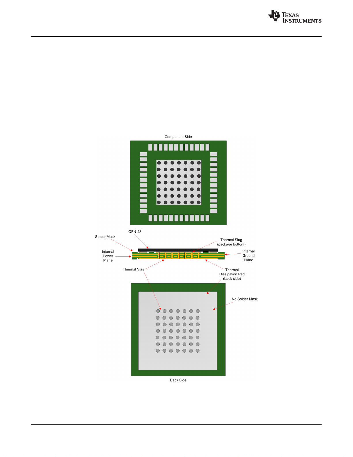
CDCM6208V1F
SCAS943 –MAY 2015
www.ti.com
13 Layout
13.1 Layout Guidelines
Employing the thermally enhanced printed circuit board layout shown in Figure 59 insures good thermal
performance of the solution. Observing good thermal layout practices enables the thermal pad on the backside of
the QFN-48 package to provide a good thermal path between the die contained within the package and the
ambient air. This thermal pad also serves as the ground connection the device; therefore, a low inductance
connection to the ground plane is essential.
13.2 Layout Example
Figure 59 shows a layout optimized for good thermal performance and a good power supply connection as well.
The 7×7 filled via pattern facilitates both considerations.
Figure 59. Recommended PCB layout of CDCM6208
74 Submit Documentation Feedback Copyright © 2015, Texas Instruments Incorporated
Product Folder Links: CDCM6208V1F
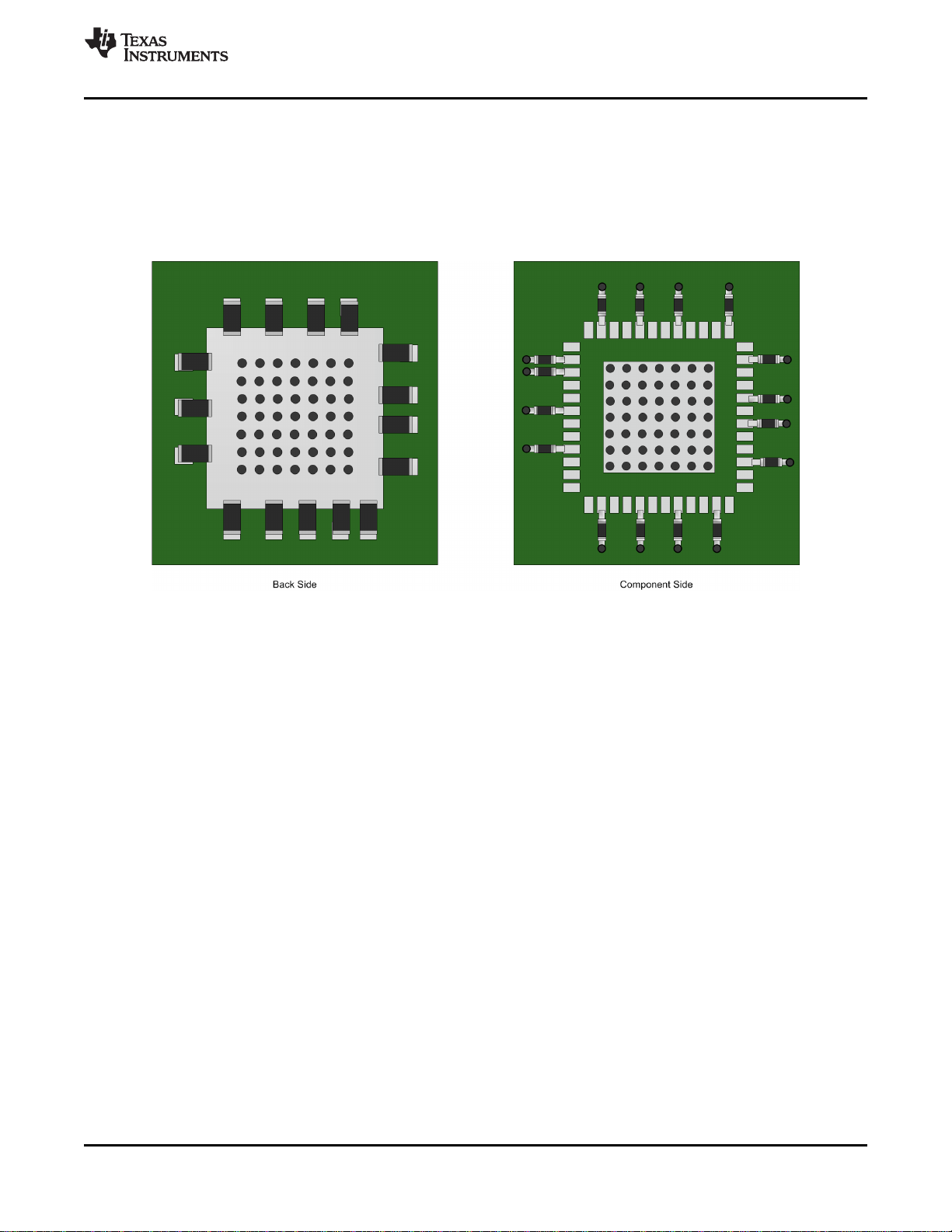
CDCM6208V1F
www.ti.com
SCAS943 –MAY 2015
Layout Example (continued)
Figure 60 shows two conceptual layouts detailing recommended placement of power supply bypass capacitors. If
the capacitors are mounted on the back side, 0402 components can be employed; however, soldering to the
Thermal Dissipation Pad can be difficult. For component side mounting, use 0201 body size capacitors to
facilitate signal routing. Keep the connections between the bypass capacitors and the power supply on the
device as short as possible. Ground the other side of the capacitor using a low impedance connection to the
ground plane.
Figure 60. PCB Conceptual Layouts
Copyright © 2015, Texas Instruments Incorporated Submit Documentation Feedback 75
Product Folder Links: CDCM6208V1F

5
5
4
4
3
3
2
2
1
1
D D
C C
B B
A A
01
CDCM6208 Reference Schematic
1 3December, 2011
Title
Rev
Date: Sheet
of
DNI
C308
1uF
C291
0.1uF
0.1uF
C303
0.1uF
C286
1uF
0.1uF
C279
0.1uF
C274
0.1uF
0.1uF
C82
10uF/6.3V
0.1uF
C275
1uF
DNI
0.1uF
C305
1uF
C295
0.1uF
DNI
C300
1uF
C285
0.1uF
C284
0.1uF
U1
SI_MODE0
1
SDI/SDA/PIN1
2
SDO/AD0/PIN2
3
SCS/AD1/PIN3
4
SCL/PIN4
5
REF_SEL
6
VDD_PRI_REF
7
PRI_REFP
8
PRI_REFN
9
VDD_SEC_REF
10
SEC_REFP
11
SEC_REFN
12
Y4_N
25
Y4_P
26
VDD_Y4
27
Y5_N
28
Y5_P
29
VDD_Y5
30
VDD_Y6
31
Y6_P
32
Y6_N
33
VDD_Y7
34
Y7_P
35
Y7_N
36
VDD_PLL137VDD_PLL2
38
VDD_VCO
39
REG_CAP
40
ELF
41
SYNCN
42
PDN
43
RESETN/PWR
44
STATUS1/PIN0
45
STATUS0
46
SI_MODE1
47
DVDD
48
POWER_PAD
49
VDD1_Y0_Y113Y0_P14Y0_N15Y1_N16Y1_P17VDD2_Y0_Y118VDD1_Y2_Y319Y2_P20Y2_N21Y3_N22Y3_P23VDD2_Y2_Y3
24
CDCM6208
C282
1uF
0.1uF
DNI
C307
0.1uF
0.1uF
DNI DNI
0.1uF
L1
BLM15HD102SN1D
1 2
C298
0.1uF
0.1uF
0.1uF
C304
0.1uF
C302
1uF
C281
10uF
C287
0.1uF
C280
0.1uF
C288
0.1uF
C292
0.1uF
C290
0.1uF
C289
0.1uF
C293
1uF
0.1uF
C277
1uF
C276
1uF
0.1uF
DNI DNI
0.1uF
0.1uF
0.1uF
C301
0.1uF
C299
0.1uF
C283
100pF
DNIDNI
0.1uF
VDD_OUT01
DVDD
VDD_PLL_A
VDD_OUT7
VDD_OUT23
VDD_OUT23
VDD_OUT01
VDD_OUT01
DVDD
VDD_PLL
VDD_SEC_IN
VDD_PRI_IN
VDD_OUT6
VDD_OUT5
VDD_OUT4
REG_CAP
REG_CAP
VDD_PLL
VDD_PLL_A
RESET_PWR
VDD_OUT23
VDD_OUT4
VDD_OUT5
VDD_OUT6
VDD_OUT7
VDD_PRI_IN
VDD_SEC_IN
DVDD DVDD DVDD DVDD DVDD
DSP_CLK7P
DSP_CLK7N
DSP_CLK6P
DSP_CLK6N
DSP_CLK5N
DSP_CLK5P
DSP_CLK4N
DSP_CLK4P
REF_SEL
SCL_PIN4
SCS_AD1_PIN3
SDO_AD0_PIN2
SDI_SDA_PIN1
SI_MODE0
PRI_REFP
PRI_REFN
SEC_REFP
SEC_REFN
DSP_CLK0P
DSP_CLK0N
DSP_CLK1P
DSP_CLK1N
DSP_CLK2P
DSP_CLK2N
DSP_CLK3P
DSP_CLK3N
ELF
SYNCN
PDN
RESET_PWR
STATUS1_PIN0
STATUS0
SI_MODE1
STATUS1_PIN0 SDI_SDA_PIN1 SDO_AD0_PIN2 SCS_AD1_PIN3 SCL_PIN4
Place 10uF close to
device pin to minimize
series resistance
General Power supply related note:
Place all 0.1uF bypass caps as close as possible to device pins.
Device Reset can connect to
power monitor or left unconnected;
pin has internal 150k pullup
PWR_MONITOR
CDCM6208V1F
SCAS943 –MAY 2015
13.2.1 Reference Schematic
www.ti.com
76 Submit Documentation Feedback Copyright © 2015, Texas Instruments Incorporated
Figure 61. Schematic Page 1
Product Folder Links: CDCM6208V1F
5
5
4
4
3
3
2
2
1
1
D D
C C
B B
A A
01
CDCM6208 Reference Schematic
December, 2011
Title
Rev
Date:
Sheet
of
C1
R86
49.9
C296
1uF
R_SEC_PDN
R73
DNI
R_PRI_PUP
C28
4pF
C297
1uF
C2
R83
49.9
R84
49.9
R72
DNI
R89
0.0
R85
49.9
R_SEC_PUP
R_PRI_PDN
C27
4pF
C_PRI_N
1uF
C29
1uF
C_PRI_P
1uF
R87
0.0
C30
1uF
R2
Y1
NX3225GA
1
1
GND1
2
3
3
GND0
4
25MHz
VDD_SEC_IN
CLKIN_SECP
CLKIN_SECN
VDD_PRI_IN
CLKIN_PRIP
CLKIN_PRIN
PRI_REFP
PRI_REFN
SEC_REFP
SEC_REFN
ELF
PRIMARY REFERENCE INPUT
SECONDARY REFERENCE INPUT
Loop Filter
Examples:
LOOP FILTER
Synthesizer mode (high loop bandwidth)
CDCM6208V1:
With C1=100pF, R2=500Ö, C2=22nF and
Internal components R3=100Ö, C3=242.5pF,
f
PFD
=25MHz, and ICP=2.5mA:
Loop bandwidth ~ (300kHz)
CDCM6208V2:
With C1=470pF, R2=560Ö, C2=100nF and
Internal components R3=100Ö, C3=242.5pF,
f
PFD
=30.72MHz, and ICP=2.5mA:
Loop bandwidth ~ (300kHz)
Jitter cleaner mode (low loop bandwidth):
CDCM6208V1:
With C1=4.7éF, R2=145Ö, C2=47éF and
Internal components R3=4.01kÖ, C3=662.5pF,
f
PFD
=40kHz, and ICP=500éA:
Loop bandwidth ~ (40Hz)
CDCM6208V2:
With C1=5éF, R2=100Ö, C2=100éF and
Internal components R3=4.01kÖ, C3=662.5pF,
f
PFD
=80kHz, and ICP=500éA:
Loop bandwidth ~ (100Hz)
2 3
The following input biasing is recommended:
AC coupled differential signals with VDD_PRI/SEC=2.5/3.3V:
select Reg4[7:6]=01 and/or Reg4[4:3]=01 (LVDS),
target V
BIAS
=1.2V, therefore
set R_PRI_PUP=5.5k, RPRI_PDN=3.14k
D
C coupled LVDS signals with VDD_PRI/SEC=2.5/3.3V:
select Reg4[7:6]=01 and/or Reg4[4:3]=01 (LVDS),
R_PRI_PUP=5.5k, RPRI_PDN=3.14k
replace C_PRI_P=C_PRI_N=0Ö
D
C coupled 3.3V CMOS signals:
Connect VDD_SEC_IN=3.3V,
select Reg4[7:6]=10 and/or Reg4[4:3]=10 (CMOS),
R83,R84,R85, & R86=DNI, replace C_PRI_P=C_PRI_N=0Ö
f
or VDD_PRI/SEC=1.8V:
target V
BIAS
=0.9V, therefore
set R_PRI_PUP=5.5k, RPRI_PDN=5.5k
f
or VDD_PRI/SEC=1.8V:
R_PRI_PUP=5.5k, RPRI_PDN=3.14k
f
or 1.8V CMOS signals:
Connect VDD_SEC_IN=1.8V:
DC coupled CML only (VDD_PRI/6(&YROWDJHLVGRQ¬WFDUH):
select Reg4[7:6]=00 and/or Reg4[4:3]=00 (CML),
set R_PRI_PUP=0Ö, RPRI_PDN=DNI,
Replace CPRI_P=0Ö, C_PRI_N=0Ö
Use of Crystal on secondary reference input (VDD_SEC_,1YROWDJHLVGRQ¬WFDUH):
select Reg4[7:6]=11 (XTAL),
set R87=DNI, R89=DNI, R72=0Ö, R73=0Ö
www.ti.com
CDCM6208V1F
SCAS943 –MAY 2015
Copyright © 2015, Texas Instruments Incorporated Submit Documentation Feedback 77
Figure 62. Schematic Page 2
Product Folder Links: CDCM6208V1F

5
5
4
4
3
3
2
2
1
1
D D
C C
B B
A A
C48
0.01uF
DNI
2
DNI
2
0
2
0
2
0
2
R58
12.5k
1 2
C38
0.01uF
R2p5
DNI
DNI
2
C51
0.01uF
R54
10k
1 2
0
2
DNI
2
DNI
2
C50
750pF
DNI
2
DNI
2
0
2
DNI
2
0
2
0
2
DNI
2
R56
10k
1 2
C39
10uF/6.3V
C53
1300pF
DNI
2
DNI
2
R41
10k
1 2
U7
OUT1
1
OUT2
2
FB
3
GND
4
EN
5
NR
6
IN2
7
IN1
8
GND_PAD
9
TPS7A8001
DNI
2
DNI
2
DNI
2
C35
10uF/6.3V
C34
10uF/6.3V
0
2
0
2
C49
10uF/6.3V
R40
30.9k
1 2
DNI
2
DNI
2
DNI
2
U8
OUT1
1
OUT2
2
FB
3
GND
4
EN
5
NR
6
IN2
7
IN1
8
GND_PAD
9
TPS7A8001
C37
510pF
R3p3
DNI
DNI
2
C36
10uF/6.3V
U6
OUT1
1
OUT2
2
FB
3
GND
4
EN
5
NR
6
IN2
7
IN1
8
GND_PAD
9
TPS7A8001
R1p8
0
C52
10uF/6.3V
R55
21k
1 2
3p3V
3p3V
1p8V
2p5V
+5V
2p5V
+5V
1p8V
+5V
VDD_PLL
3p3V
1p8V
2p5V
VDD_OUT01
3p3V
1p8V
2p5V
VDD_OUT23
3p3V
1p8V
2p5V
VDD_OUT4
3p3V
1p8V
2p5V
VDD_OUT5
3p3V
1p8V
2p5V
VDD_OUT7
3p3V
1p8V
2p5V
VDD_PRI_IN
3p3V
1p8V
2p5V
VDD_SEC_IN
3p3V
1p8V
2p5V
3p3V
1p8V
2p5V
DVDD
VDD_OUT6
3.3V Power Supply
MANY VIAS with Heat Sink
2.5V Power Supply
MANY VIAS with Heat Sink
1.8V Power Supply
MANY VIAS with Heat Sink
If SPI or I2C is used, set DVDD to the same
supply voltage (e.g. 1.8V, 2.5V, or 3.3V)
VDD_OUT4, 5, 6, and VDD_OUT7 supply setting
reflect the CMOS signal output swing
01
CDCM6208 Reference Schematic
December, 2011
Title
Rev
Date:
Sheet
of
3 3
Every supply can individually be connected to either 1.8V, 2.5V, or 3.3V. It is also possible to
run all IO from one single supply at 1.8V, 2.5V, or 3.3V.
CDCM6208V1F
SCAS943 –MAY 2015
www.ti.com
Figure 63. Schematic Page 3
78 Submit Documentation Feedback Copyright © 2015, Texas Instruments Incorporated
Product Folder Links: CDCM6208V1F
PICe phy
DSP with receiver input
termination and self-
biasing
5
5
4
4
3
3
2
2
1
1
D
D
C
B B
A A
01
CDCM6208 Reference Schematic (Extra: output termination)
December, 2011
Title
Rev
Date: Sheet
of
1uF
0
1uF
49.949.9
0
Y4-7_HCSL_P
Y4-7_HCSL_N
Y0-7 LVDS_P
PCIe_PHY_N
PCIe_PHY_P
HCSL connection example (DC coupled)
Outputs 4 to 7 have option for HCSL, LVCMOS, LPCML
For HCSL, install 50 ohm termination resistors and adjust
series resistor between 0 and 33 ohms to improve ringing.
TX-line 50Ö
R
S(P)
R
S(N)
TX-line 50Ö
Diff_in_N
Diff_in_P
LVDS or LVPECL connection example (AC coupled)
TX-line 50Ö
TX-line 50Ö
Y0-7 LVDS_N
DSP without receiver
input termination and
self-biasing
1uF
1uF
Y0-7 LVDS_P
Diff_in_N
Diff_in_P
LVDS or LVPECL connection example (AC coupled)
TX-line 50Ö
TX-line 50Ö
Y0-7 LVDS_N
49.9
Vbias
100n
49.9
extra
www.ti.com
CDCM6208V1F
SCAS943 –MAY 2015
Figure 64. Schematic Page 4
Copyright © 2015, Texas Instruments Incorporated Submit Documentation Feedback 79
Product Folder Links: CDCM6208V1F

CDCM6208V1F
SCAS943 –MAY 2015
14 Device and Documentation Support
14.1 Trademarks
KeyStone is a trademark of Texas Instruments.
I2C is a trademark of NXP B.V. Corporation.
All other trademarks are the property of their respective owners.
14.2 Documentation Support
14.2.1 Related Documentation
IC Package Thermal Metrics application report, SPRA953.
Hardware Design Guide for KeyStone Devices SPRABI2 for the SRIO interface.
14.3 Electrostatic Discharge Caution
These devices have limited built-in ESD protection. The leads should be shorted together or the device placed in conductive foam
during storage or handling to prevent electrostatic damage to the MOS gates.
14.4 Glossary
SLYZ022 — TI Glossary.
This glossary lists and explains terms, acronyms, and definitions.
www.ti.com
15 Mechanical, Packaging, and Orderable Information
The following pages include mechanical, packaging, and orderable information. This information is the most
current data available for the designated devices. This data is subject to change without notice and revision of
this document. For browser-based versions of this data sheet, refer to the left-hand navigation.
80 Submit Documentation Feedback Copyright © 2015, Texas Instruments Incorporated
Product Folder Links: CDCM6208V1F
PACKAGE OPTION ADDENDUM
www.ti.com
10-Dec-2020
PACKAGING INFORMATION
Orderable Device Status
CDCM6208V1FRGZR ACTIVE VQFN RGZ 48 2500 RoHS & Green NIPDAU Level-3-260C-168 HR -40 to 85 CM6208V1F
CDCM6208V1FRGZT ACTIVE VQFN RGZ 48 250 RoHS & Green NIPDAU Level-3-260C-168 HR -40 to 85 CM6208V1F
(1)
The marketing status values are defined as follows:
ACTIVE: Product device recommended for new designs.
LIFEBUY: TI has announced that the device will be discontinued, and a lifetime-buy period is in effect.
NRND: Not recommended for new designs. Device is in production to support existing customers, but TI does not recommend using this part in a new design.
PREVIEW: Device has been announced but is not in production. Samples may or may not be available.
OBSOLETE: TI has discontinued the production of the device.
Package Type Package
(1)
Drawing
Pins Package
Qty
Eco Plan
(2)
Lead finish/
Ball material
(6)
MSL Peak Temp
(3)
Op Temp (°C) Device Marking
(4/5)
(2)
RoHS: TI defines "RoHS" to mean semiconductor products that are compliant with the current EU RoHS requirements for all 10 RoHS substances, including the requirement that RoHS substance
do not exceed 0.1% by weight in homogeneous materials. Where designed to be soldered at high temperatures, "RoHS" products are suitable for use in specified lead-free processes. TI may
reference these types of products as "Pb-Free".
RoHS Exempt: TI defines "RoHS Exempt" to mean products that contain lead but are compliant with EU RoHS pursuant to a specific EU RoHS exemption.
Green: TI defines "Green" to mean the content of Chlorine (Cl) and Bromine (Br) based flame retardants meet JS709B low halogen requirements of <=1000ppm threshold. Antimony trioxide based
flame retardants must also meet the <=1000ppm threshold requirement.
(3)
MSL, Peak Temp. - The Moisture Sensitivity Level rating according to the JEDEC industry standard classifications, and peak solder temperature.
(4)
There may be additional marking, which relates to the logo, the lot trace code information, or the environmental category on the device.
(5)
Multiple Device Markings will be inside parentheses. Only one Device Marking contained in parentheses and separated by a "~" will appear on a device. If a line is indented then it is a continuation
of the previous line and the two combined represent the entire Device Marking for that device.
(6)
Lead finish/Ball material - Orderable Devices may have multiple material finish options. Finish options are separated by a vertical ruled line. Lead finish/Ball material values may wrap to two
lines if the finish value exceeds the maximum column width.
Important Information and Disclaimer:The information provided on this page represents TI's knowledge and belief as of the date that it is provided. TI bases its knowledge and belief on information
provided by third parties, and makes no representation or warranty as to the accuracy of such information. Efforts are underway to better integrate information from third parties. TI has taken and
continues to take reasonable steps to provide representative and accurate information but may not have conducted destructive testing or chemical analysis on incoming materials and chemicals.
TI and TI suppliers consider certain information to be proprietary, and thus CAS numbers and other limited information may not be available for release.
In no event shall TI's liability arising out of such information exceed the total purchase price of the TI part(s) at issue in this document sold by TI to Customer on an annual basis.
Samples
Addendum-Page 1

PACKAGE OPTION ADDENDUM
www.ti.com
10-Dec-2020
Addendum-Page 2

PACKAGE MATERIALS INFORMATION
www.ti.com 15-May-2015
TAPE AND REEL INFORMATION
*All dimensions are nominal
Device Package
CDCM6208V1FRGZR VQFN RGZ 48 2500 330.0 16.4 7.3 7.3 1.1 12.0 16.0 Q2
CDCM6208V1FRGZT VQFN RGZ 48 250 180.0 16.4 7.3 7.3 1.1 12.0 16.0 Q2
Type
Package
Drawing
Pins SPQ Reel
Diameter
(mm)
Reel
Width
W1 (mm)
A0
(mm)B0(mm)K0(mm)P1(mm)W(mm)
Pin1
Quadrant
Pack Materials-Page 1

PACKAGE MATERIALS INFORMATION
www.ti.com 15-May-2015
*All dimensions are nominal
Device Package Type Package Drawing Pins SPQ Length (mm) Width (mm) Height (mm)
CDCM6208V1FRGZR VQFN RGZ 48 2500 367.0 367.0 38.0
CDCM6208V1FRGZT VQFN RGZ 48 250 210.0 185.0 35.0
Pack Materials-Page 2

GENERIC PACKAGE VIEW
VQFN - 1 mm max heightRGZ 48
7 x 7, 0.5 mm pitch
PLASTIC QUADFLAT PACK- NO LEAD
Images above are just a representation of the package family, actual package may vary.
Refer to the product data sheet for package details.
www.ti.com
4224671/A

PACKAGE OUTLINE
PIN 1 INDEX AREA
1 MAX
SCALE 2.000
B
7.15
6.85
A
7.15
6.85
VQFN - 1 mm max heightRGZ0048B
PLASTIC QUAD FLATPACK - NO LEAD
C
SEATING PLANE
0.05
0.00
44X 0.5
2X
5.5
PIN 1 ID
(OPTIONAL)
12
2X 5.5
4.1 0.1
13
49
1
48
SYMM
48X
24
25
SYMM
36
37
0.5
0.3
0.08 C
EXPOSED
THERMAL PAD
0.30
48X
0.18
0.1 C B A
0.05
(0.2) TYP
4218795/B 02/2017
NOTES:
1. All linear dimensions are in millimeters. Any dimensions in parenthesis are for reference only. Dimensioning and tolerancing
per ASME Y14.5M.
2. This drawing is subject to change without notice.
3. The package thermal pad must be soldered to the printed circuit board for thermal and mechanical performance.
www.ti.com

48X (0.24)
44X (0.5)
48X (0.6)
SYMM
EXAMPLE BOARD LAYOUT
VQFN - 1 mm max heightRGZ0048B
PLASTIC QUAD FLATPACK - NO LEAD
( 4.1)
(1.115) TYP
(0.685)
48
1
TYP
49
37
36
(1.115)
TYP
(0.685)
TYP
( 0.2) TYP
VIA
(R0.05)
TYP
0.07 MAX
ALL AROUND
EXPOSED METAL
12
13
SYMM
(6.8)
LAND PATTERN EXAMPLE
EXPOSED METAL SHOWN
SCALE:12X
ALL AROUND
METAL
EXPOSED METAL
SOLDER MASK
OPENING
(6.8)
25
24
0.07 MIN
SOLDER MASK
OPENING
METAL UNDER
SOLDER MASK
NON SOLDER MASK
DEFINED
(PREFERRED)
SOLDER MASK
DEFINED
SOLDER MASK DETAILS
4218795/B 02/2017
NOTES: (continued)
4. This package is designed to be soldered to a thermal pad on the board. For more information, see Texas Instruments literature
number SLUA271 (www.ti.com/lit/slua271).
5. Vias are optional depending on application, refer to device data sheet. If any vias are implemented, refer to their locations shown
on this view. It is recommended that vias under paste be filled, plugged or tented.
www.ti.com

48X (0.6)
48X (0.24)
EXAMPLE STENCIL DESIGN
VQFN - 1 mm max heightRGZ0048B
PLASTIC QUAD FLATPACK - NO LEAD
(1.37)
48
1
TYP
37
36
44X (0.5)
(R0.05) TYP
METAL
TYP
SYMM
49
12
13
SYMM
(6.8)
SOLDER PASTE EXAMPLE
BASED ON 0.125 mm THICK STENCIL
EXPOSED PAD 49
73% PRINTED SOLDER COVERAGE BY AREA UNDER PACKAGE
SCALE:12X
24
(1.37)
(
25
TYP
(6.8)
9X
1.17)
4218795/B 02/2017
NOTES: (continued)
6. Laser cutting apertures with trapezoidal walls and rounded corners may offer better paste release. IPC-7525 may have alternate
design recommendations.
www.ti.com

IMPORTANT NOTICE AND DISCLAIMER
TI PROVIDES TECHNICAL AND RELIABILITY DATA (INCLUDING DATASHEETS), DESIGN RESOURCES (INCLUDING REFERENCE
DESIGNS), APPLICATION OR OTHER DESIGN ADVICE, WEB TOOLS, SAFETY INFORMATION, AND OTHER RESOURCES “AS IS”
AND WITH ALL FAULTS, AND DISCLAIMS ALL WARRANTIES, EXPRESS AND IMPLIED, INCLUDING WITHOUT LIMITATION ANY
IMPLIED WARRANTIES OF MERCHANTABILITY, FITNESS FOR A PARTICULAR PURPOSE OR NON-INFRINGEMENT OF THIRD
PARTY INTELLECTUAL PROPERTY RIGHTS.
These resources are intended for skilled developers designing with TI products. You are solely responsible for (1) selecting the appropriate
TI products for your application, (2) designing, validating and testing your application, and (3) ensuring your application meets applicable
standards, and any other safety, security, or other requirements. These resources are subject to change without notice. TI grants you
permission to use these resources only for development of an application that uses the TI products described in the resource. Other
reproduction and display of these resources is prohibited. No license is granted to any other TI intellectual property right or to any third
party intellectual property right. TI disclaims responsibility for, and you will fully indemnify TI and its representatives against, any claims,
damages, costs, losses, and liabilities arising out of your use of these resources.
TI’s products are provided subject to TI’s Terms of Sale (www.ti.com/legal/termsofsale.html) or other applicable terms available either on
ti.com or provided in conjunction with such TI products. TI’s provision of these resources does not expand or otherwise alter TI’s applicable
warranties or warranty disclaimers for TI products.
Mailing Address: Texas Instruments, Post Office Box 655303, Dallas, Texas 75265
Copyright © 2020, Texas Instruments Incorporated
 Loading...