

Page 1
www.ti.com
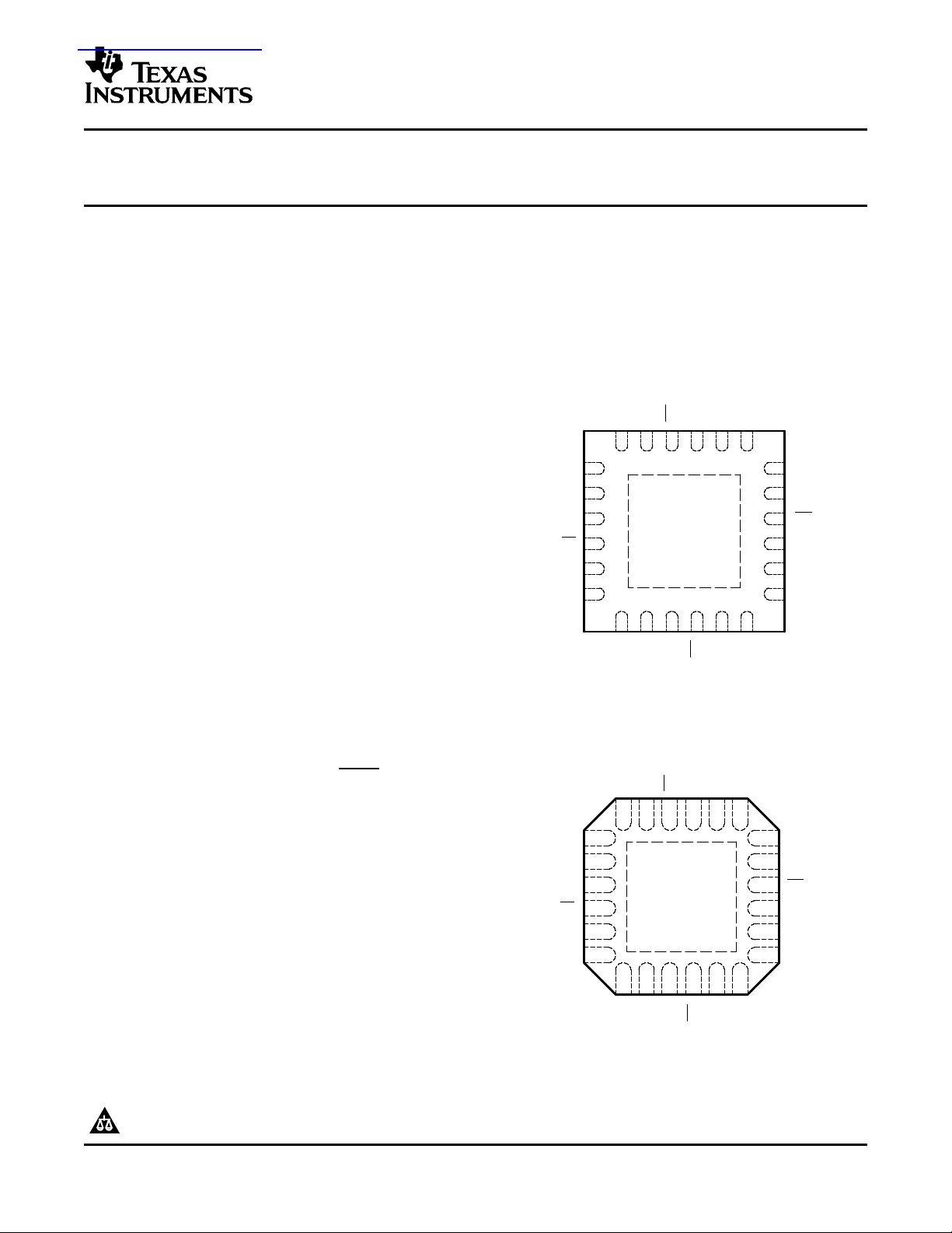
V
SS
(1)
S0
VDD1
Y1
Y1
VDD1
VDD3
18
17
16
15
14
13
1
2
3
4
5
6
EN
VDDPECL
IN
IN
VDDPECL
VBB
24 23 22 21 20 19
7 8 9 10 11 12
S2
V
DD
0
Y0
Y0
V
DD
0
S1
V
SS
V
DD
2
Y2
Y2
V
DD
2
Y3
RGE PACKAGE
(TOP VIEW)
(1)
Thermal pad must be connected to VSS.
P0024-01
(1)
Thermal pad must be connected to VSS.
P0025-01
18
17
16
15
14
13
S0
VDD1
Y1
Y1
VDD1
VDD3
1
2
3
4
5
6
7
8
9
10
11
12
24
23
22
21
20
19
EN
VDDPECL
IN
IN
VDDPECL
VBB
S2
V
DD
0
Y0Y0V
DD
0
S1
V
SS
V
DD
2
Y2
Y2
V
DD
2
Y3
V
SS
(1)
RTH PACKAGE
(TOP VIEW)
查询CDCM1804供应商
LVCMOS OUTPUT AND PROGRAMMABLE DIVIDER
CDCM1804
SCAS697E – JULY 2003 – REVISED MAY 2005
1:3 LVPECL CLOCK BUFFER + ADDITIONAL
FEATURES
• Distributes One Differential Clock Input to
Three LVPECL Differential Clock Outputs and
One LVCMOS Single-Ended Output
• Programmable Output Divider for Two
LVPECL Outputs and LVCMOS Output
• Low-Output Skew 15 ps (Typical) for
Clock-Distribution Applications for LVPECL
Outputs; 1.6-ns Output Skew Between
LVCMOS and LVPECL Transitions Minimizing
Noise
• V
• Signaling Rate Up to 800-MHz LVPECL and
• Differential Input Stage for Wide
• Provides VBB Bias Voltage Output for
• Receiver Input Threshold ± 75 mV
• 24-Terminal QFN Package (4 mm × 4 mm)
• Accepts Any Differential Signaling:
Range 3 V–3.6 V
CC
200-MHz LVCMOS
Common-Mode Range
Single-Ended Input Signals
LVDS, HSTL, CML, VML, SSTL-2, and
Single-Ended: LVTTL/LVCMOS
The CDCM1804 is characterized for operation from
–40 ° C to 85 ° C.
For use in single-ended driver applications, the
CDCM1804 also provides a VBB output terminal that
can be directly connected to the unused input as a
common-mode voltage reference.
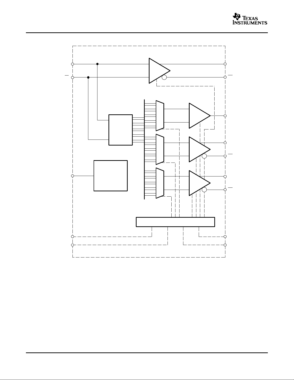
DESCRIPTION
The CDCM1804 clock driver distributes one pair of
differential clock inputs to three pairs of LVPECL
differential clock outputs Y[2:0] and Y[2:0], with minimum skew for clock distribution. The CDCM1804 is
specifically designed for driving 50- Ω transmission
lines. Additionally, the CDCM1804 offers a
single-ended LVCMOS output Y3. This output is
delayed by 1.6 ns over the three LVPECL output
stages to minimize noise impact during signal transitions.
The CDCM1804 has three control terminals, S0, S1,
and S2, to select different output mode settings. The
S[2:0] terminals are 3-level inputs and therefore allow
up to 33= 27 combinations. Additionally, an enable
terminal (EN) is provided to disable or enable all
outputs simultaneously. The EN terminal is a 3-level
input as well and extends the number of settings to
2 × 27 = 54. See Table 1 for details.
PRODUCTION DATA information is current as of publication date.
Products conform to specifications per the terms of the Texas
Instruments standard warranty. Production processing does not
necessarily include testing of all parameters.
Please be aware that an important notice concerning availability, standard warranty, and use in critical applications of Texas
Instruments semiconductor products and disclaimers thereto appears at the end of this data sheet.
Copyright © 2003–2005, Texas Instruments Incorporated
Page 2
www.ti.com
Control
VBB
LVPECL
Y1
Y1
LVPECL
Y2
Y2
LVPECL
Y3
LVCMOS
Y0
Y0
Div 1
Div 2
Div 4
Div 8
Div 16
Bias
Generator
VDD − 1.3 V
(I
max
< 1.5 mA)
IN
IN
S2
ENS0
S1
B0059-01
CDCM1804
SCAS697E – JULY 2003 – REVISED MAY 2005
FUNCTIONAL BLOCK DIAGRAM
2
Page 3
www.ti.com
CDCM1804
SCAS697E – JULY 2003 – REVISED MAY 2005
TERMINAL FUNCTIONS
TERMINAL
NAME NO.
EN 1 I ENABLE: Enables or disables all outputs simultaneously. The EN terminal offers three
IN, IN 3, 4 I (differential) Differential input clock: Input stage is sensitive and has a wide common-mode range.
S[2:0] 18, 19, 24 I Select mode of operation: Defines the output configuration of Y[3:0]. Each terminal
VBB 6 O Bias voltage output to be used to bias unused complementary input IN for single-ended
V
SS
VDDPECL 2, 5 Supply Supply voltage LVPECL input + internal logic
VDD[2:0] 8, 11, 14, Supply LVPECL output supply voltage for output Y[2:0]. Each output can be disabled by pulling
VDD3 13 Supply Supply voltage LVCMOS output. The LVCMOS output can be disabled by pulling VDD3
Y[2:0] 9, 15, 21 O (LVPECL) LVPECL clock outputs. These outputs provide low-skew copies of IN or down-divided
Y[2:0] 10, 16, 22 copies of clock IN based on selected mode of operation S[2:0]. If an output is unused,
Y3 12 O LVCMOS clock output. This output provides copy of IN or down-divided copy of clock IN
7 Supply Device ground
17, 20, 23 the corresponding VDDx to GND.
I/O DESCRIPTION
(with 60-k Ω pullup) different configurations: tied to GND (logic 0), external 60-k Ω pulldown resistor (pull to
(with 60-k Ω pullup) offers three different configurations: tied to GND (logic 0), external 60-k Ω pulldown
VDD/2), or left floating (logic 1);
EN = 1: outputs on according to S[2:0] settings
EN = VDD/2: outputs on according to S[2:0] settings
EN = 0: outputs Y[3:0] off (high impedance)
See Table 1 for details.
Therefore, almost any type of differential signal can drive this input (LVPECL, LVDS,
CML, HSTL). Because the input is high-impedance, it is recommended to terminate the
PCB transmission line before the input (e.g., with 100 Ω across input). Input can also be
driven by single-ended signal if the complementary input is tied to VBB. A
more-advanced scheme for single-ended signals is given in the Application Information
section near the end of this document.
The inputs employ an ESD structure protecting the inputs in case of an input voltage
exceeding the rails by more than ~0.7 V. Reverse biasing of the IC through these inputs
is possible and must be prevented by limiting the input voltage < VDD.
resistor (pull to VDD/2), or left floating (logic 1); see Table 1 for details.
input signals.
The output voltage of VBB is V
is limited to about 1.5 mA.
CAUTION: In this mode, no voltage from outside may be forced, because internal
diodes could be forced in forward direction. Thus, it is recommended to disconnect the
output.
to GND.
CAUTION: In this mode, no voltage from outside may be forced because internal
diodes could be forced in a forward direction. Thus, it is recommended to leave Y3
unconnected, tied to GND, or terminated into GND.
the output can simply be left open to save power and minimize noise impact to the
remaining outputs.
based on selected mode of operation S[2:0]. Also, this output can be disabled when
VDD3 becomes tied to GND.
– 1.3 V. When driving a load, the output current drive
DD
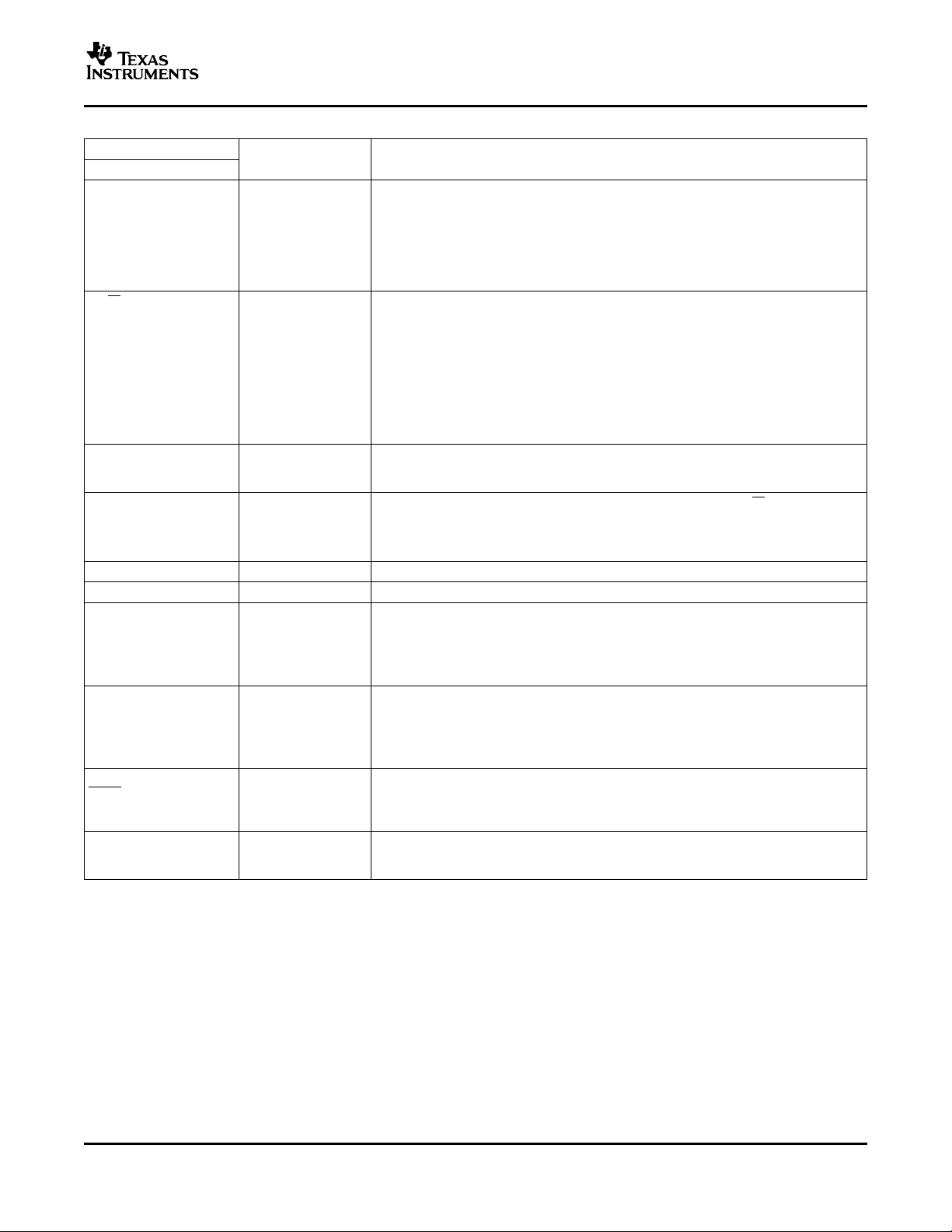
CONTROL TERMINAL SETTINGS
The CDCM1804 has three control terminals (S0, S1, and S2) and an enable terminal (EN) to select different
output mode settings. All four inputs (S0, S1, S2, and EN) are 3-level inputs offering 54 different combinations. In
addition, the EN input allows the disabling of all outputs and forcing them into a high-z (or 3-state) output state
when pulled to GND.
Each control input incorporates a 60-k Ω pullup resistor. Thus, it is easy to choose the input setting by designing
a resistor pad between the control input and GND. To choose a logic zero, the resistor value must be zero.
Setting the input high requires leaving the resistor pad empty (no resistor installed). For setting the input to
V
/2, the installed resistor must be a 60-k Ω pulldown to GND with a 10% tolerance or better.
DD
3
Page 4
www.ti.com
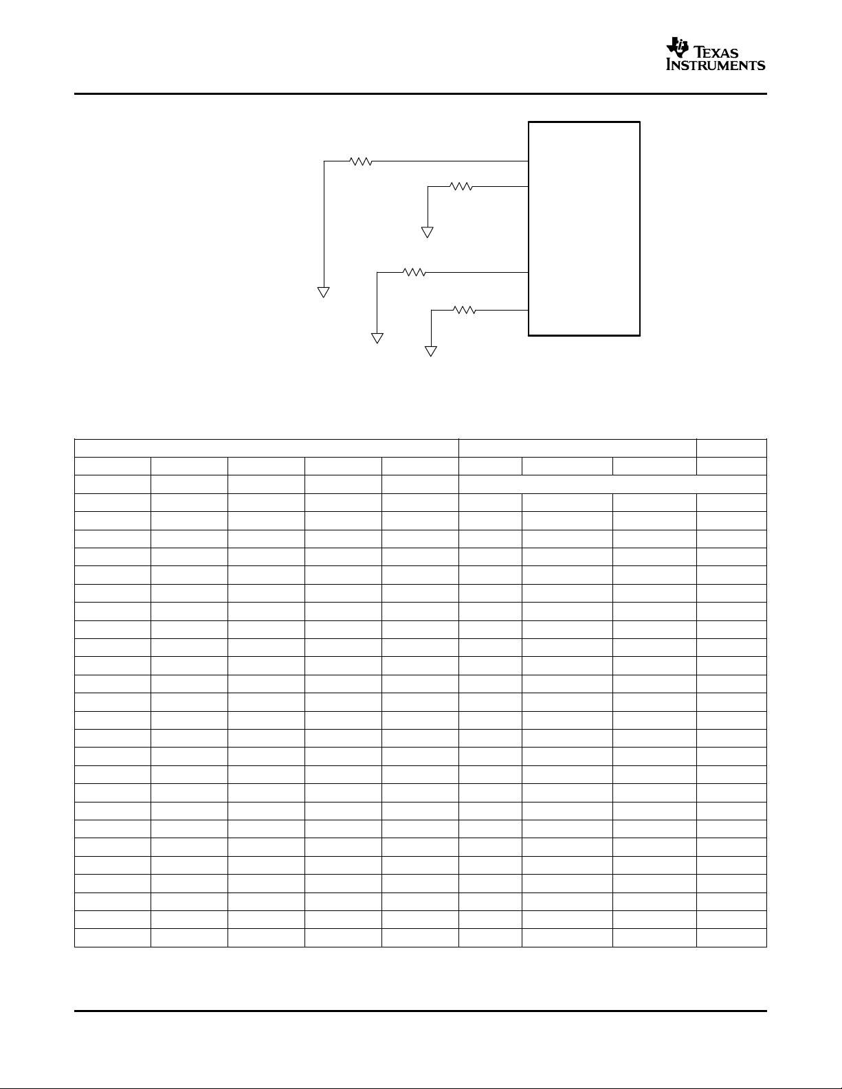
RS0 = 0 Ω
EN
CDCM1804
S1
S0
RS1 = 60 kΩ
REN = Open
Setting for Mode 13:
EN = 1
S2 = VDD/2
S1 = VDD/2
S0 = 0
RS2 = 60 kΩ
S2
S0084-01
CDCM1804
SCAS697E – JULY 2003 – REVISED MAY 2005
Figure 1. Control Terminal Setting for Example
Table 1. Selection Mode Table
LVPECL
MODE EN S2 S1 S0 Y0 Y1 Y2 Y3
0 0 x x x Off (high-z)
1 1 0 0 0 ÷ 1 ÷ 1 ÷ 1 Off (high-z)
2 1 0 0 VDD/2 ÷ 1 Off (high-z) Off (high-z) ÷ 4
3 1 0 0 1 ÷ 1 ÷ 1 Off (high-z) ÷ 4
4 1 0 VDD/2 0 ÷ 1 ÷ 2 Off (high-z) ÷ 4
5 1 0 VDD/2 VDD/2 ÷ 1 ÷ 4 Off (high-z) ÷ 4
6 1 0 VDD/2 1 ÷ 1 ÷ 8 Off (high-z) ÷ 4
7 1 0 1 0 ÷ 1 Off (high-z) ÷ 1 ÷ 4
8 1 0 1 VDD/2 ÷ 1 ÷ 1 ÷ 1 ÷ 4
9 1 0 1 1 ÷ 1 ÷ 2 ÷ 1 ÷ 4
10 1 VDD/2 0 0 ÷ 1 ÷ 4 ÷ 1 ÷ 4
11 1 VDD/2 0 VDD/2 ÷ 1 ÷ 8 ÷ 1 ÷ 4
12 1 VDD/2 0 1 ÷ 1 Off (high-z) ÷ 2 ÷ 4
13 1 VDD/2 VDD/2 0 ÷ 1 ÷ 1 ÷ 2 ÷ 4
14 1 VDD/2 VDD/2 VDD/2 ÷ 1 ÷ 2 ÷ 2 ÷ 4
15 1 VDD/2 VDD/2 1 ÷ 1 ÷ 4 ÷ 2 ÷ 4
16 1 VDD/2 1 0 ÷ 1 ÷ 8 ÷ 2 ÷ 4
17 1 VDD/2 1 VDD/2 ÷ 1 Off (high-z) ÷ 4 ÷ 4
18 1 VDD/2 1 1 ÷ 1 ÷ 1 ÷ 4 ÷ 4
19 1 1 0 0 ÷ 1 ÷ 2 ÷ 4 ÷ 4
20 1 1 0 VDD/2 ÷ 1 ÷ 4 ÷ 4 ÷ 4
21 1 1 0 1 ÷ 1 ÷ 8 ÷ 4 ÷ 4
22 1 1 VDD/2 0 ÷ 1 Off (high-z) ÷ 8 ÷ 4
23 1 1 VDD/2 VDD/2 ÷ 1 ÷ 1 ÷ 8 ÷ 4
24 1 1 VDD/2 1 ÷ 1 ÷ 2 ÷ 8 ÷ 4
25 1 1 1 0 ÷ 1 ÷ 4 ÷ 8 ÷ 4
(1)
LVCMOS
(1) The LVPECL outputs are open-emitter stages. Thus, if you leave the unused LVPECL outputs Y0, Y1, or Y2 unconnected, then the
current consumption is minimized and noise impact to remaining outputs is neglectable. Also, each output can be individually disabled
by connecting the corresponding V
4
DD
input to GND.
Page 5
www.ti.com
CDCM1804
SCAS697E – JULY 2003 – REVISED MAY 2005
Table 1. Selection Mode Table (continued)
LVPECL
MODE EN S2 S1 S0 Y0 Y1 Y2 Y3
26 1 1 1 VDD/2 ÷ 1 ÷ 8 ÷ 8 ÷ 4
27 1 1 1 1 ÷ 1 Off (high-z) ÷ 16 ÷ 4
28 VDD/2 0 0 0 ÷ 1 ÷ 1 ÷ 16 ÷ 4
29 VDD/2 0 0 VDD/2 ÷ 1 ÷ 2 ÷ 16 ÷ 4
30 VDD/2 0 0 1 ÷ 1 ÷ 4 ÷ 16 ÷ 4
31 VDD/2 0 VDD/2 0 ÷ 1 ÷ 8 ÷ 16 ÷ 4
32 VDD/2 0 VDD/2 VDD/2 ÷ 1 Off (high-z) Off (high-z) ÷ 1
33 VDD/2 0 VDD/2 1 ÷ 1 ÷ 1 Off (high-z) ÷ 1
34 VDD/2 0 1 0 ÷ 1 ÷ 2 Off (high-z) ÷ 1
35 VDD/2 0 1 VDD/2 ÷ 1 ÷ 1 Off (high-z) ÷ 2
36 VDD/2 0 1 1 ÷ 1 ÷ 2 Off (high-z) ÷ 2
37 VDD/2 VDD/2 0 0 ÷ 1 Off (high-z) Off (high-z) ÷ 2
38 VDD/2 VDD/2 0 VDD/2 ÷ 1 ÷ 1 ÷ 1 ÷ 2
39 VDD/2 VDD/2 0 1 ÷ 1 ÷ 2 ÷ 8 ÷ 2
40 VDD/2 VDD/2 VDD/2 0 ÷ 1 ÷ 2 ÷ 8 ÷ 8
41 VDD/2 VDD/2 VDD/2 VDD/2 ÷ 1 ÷ 4 Off (high-z) ÷ 1
42 VDD/2 VDD/2 VDD/2 1 ÷ 1 ÷ 8 Off (high-z) ÷ 1
43 VDD/2 VDD/2 1 0 ÷ 1 ÷ 4 Off (high-z) ÷ 2
44 VDD/2 VDD/2 1 VDD/2 ÷ 1 ÷ 8 Off (high-z) ÷ 2
45 VDD/2 VDD/2 1 1 ÷ 1 ÷ 1 ÷ 2 ÷ 2
46 VDD/2 1 0 0 ÷ 1 Off (high-z) Off (high-z) ÷ 8
47 VDD/2 1 0 VDD/2 ÷ 1 ÷ 4 Off (high-z) ÷ 8
48 VDD/2 1 0 1 ÷ 1 ÷ 4 ÷ 8 ÷ 8
49 VDD/2 1 VDD/2 0 ÷ 1 ÷ 8 Off (high-z) ÷ 8
50 VDD/2 1 VDD/2 VDD/2 ÷ 1 ÷ 2 ÷ 8 ÷ 16
Rsv VDD/2 1 VDD/2 1 Reserved Reserved Reserved Reserved
Rsv VDD/2 1 1 0 N/A Low Low Low
53 VDD/2 1 1 VDD/2 ÷ 1 ÷ 1 ÷ 1 ÷ 1
54 VDD/2 1 1 1 ÷ 1 ÷ 1 ÷ 1 ÷ 1
(1)
LVCMOS
ABSOLUTE MAXIMUM RATINGS
over operating free-air temperature (unless otherwise noted)
V
DD
V
I
V
O
T
stg
T
J
(1) Stresses beyond those listed under "absolute maximum ratings" may cause permanent damage to the device. These are stress ratings
Supply voltage –0.3 V to 3.8 V
Input voltage –0.2 V to (V
Output voltage –0.2 V to (V
Differential short-circuit current, Yn, Yn, I
OSD
Electrostatic discharge (HBM 1.5 k Ω , 100 pF), ESD >2000 V
Moisture level 24-terminal QFN package (solder reflow temperature of 235 ° C) MSL 2
Storage temperature –65 ° C to 150 ° C
Maximum junction temperature 125 ° C
only, and functional operation of the device at these or any other conditions beyond those indicated under "recommended operating
conditions" is not implied. Exposure to absolute-maximum-rated conditions for extended periods may affect device reliability.
(1)
DD
DD
Continuous
+ 0.2 V)
+ 0.2 V)
5
Page 6
www.ti.com
CDCM1804
SCAS697E – JULY 2003 – REVISED MAY 2005
RECOMMENDED OPERATING CONDITIONS
V
DD
T
A
ELECTRICAL CHARACTERISTICS
over recommended operating free-air temperature range (unless otherwise noted)
LVPECL INPUT IN, IN
f
clk
V
CM
V
IN
I
IN
R
IN
C
I
(1) Is required to maintain ac specifications
(2) Is required to maintain device functionality
Supply voltage 3 3.3 3.6 V
Operating free-air temperature –40 85 ° C
PARAMETER TEST CONDITIONS MIN TYP MAX UNIT
Input frequency 0 800 MHz
High-level input common mode 1 V
Input voltage swing between IN and IN
Input voltage swing between IN and IN
Input current VI= V
(1)
(2)
or 0 V ± 10 µ A
DD
Input impedance 300 k Ω
Input capacitance at IN, IN 1 pF
MIN TYP MAX UNIT
DD
500 1300
150 1300
– 0.3 V
mV
LVPECL OUTPUT DRIVER Y[2:0], Y[2:0]
PARAMETER TEST CONDITIONS MIN TYP MAX UNIT
f
clk
V
OH
V
OL
V
O
I
OZL
I
OZH
tr/t
f
t
skpecl(o)
t
Duty
t
sk(pp)
C
O
Output frequency, see Figure 4 0 800 MHz
High-level output voltage Termination with 50 Ω to V
Low-level output voltage Termination with 50 Ω to V
Output voltage swing between Y and
Y, see Figure 4 .
Output 3-state current µ A
Rise and fall time 200 350 ps
Output skew between any LVPECL
output Y[2-0] and Y[2-0]
Output duty-cycle distortion
(1)
Termination with 50 Ω to V
V
= 3.6 V, VO= 0 V 5
DD
V
= 3.6 V, VO= V
DD
20% to 80% of V
ure 9 .
DD
OUTPP
See Note A in Figure 8 . 15 30 ps
Crossing point-to-crossing point dis-
tortion
– 2 V V
DD
– 2 V V
DD
– 2 V 500 mV
DD
– 1.18 V
DD
– 1.98 V
DD
DD
DD
– 0.8 V 10
, see Fig-
–50 50 ps
– 0.81 V
– 1.55 V
Part-to-part skew Any Y, see Note B in Figure 8 . 50 ps
Output capacitance VO= V
or GND 1 pF
DD
LOAD Expected output load 50 Ω
(1) For an 800-MHz signal, the 50-ps error would result in a duty-cycle distortion of ± 4% when driven by an ideal clock input signal.
LVPECL INPUT-TO-LVPECL OUTPUT PARAMETERS
PARAMETER TEST CONDITIONS MIN TYP MAX UNIT
LVPECL INPUT-TO-LVPECL OUTPUT PARAMETER
t
pd(lh)
t
pd(hl)
t
sk(p)
Propagation delay rising edge VOX to VOX 320 600 ps
Propagation delay falling edge VOX to VOX 320 600 ps
LVPECL pulse skew VOX to VOX, see Note C in Fig- 100 ps
ure 8 .
6
Page 7
www.ti.com
CDCM1804
SCAS697E – JULY 2003 – REVISED MAY 2005
LVCMOS OUTPUT PARAMETER, Y3
PARAMETER TEST CONDITIONS MIN TYP MAX UNIT
f
clk
t
skLVCMOS(o)
t
sk(pp)
V
OH
V
OL
I
OH
I
OL
I
OZ
C
O
t
Duty
t
pd(lh)
t
pd(hl)
t
r
t
f
OUTPUT frequency, see Figure 5
Output skew between the LVCMOS out-
put Y3 and LVPECL outputs Y[2:0]
Part-to-part skew Y3, see Note B in Figure 8 . 300 ps
High-level output voltage V
Low-level output voltage V
High-level output current V
Low-level output current V
High-impedance-state output current V
Output capacitance V
Output duty cycle distortion
Propagation delay rising edge from IN to
Y3
Propagation delay falling edge from IN
to Y3
Output rise slew rate 20% to 80% of swing, see Figure 10 . 1.4 2.3 V/ns
Output fall slew rate 80% to 20% of swing, see Figure 10 . 1.4 2.3 V/ns
(1) Operating the CDCM1804 LVCMOS output above the maximum frequency does not cause a malfunction to the device, but the Y3
output will not achieve enough signal swing to meet the output specification. Therefore, the CDCM1804 can be operated at higher
frequencies, while the LVCMOS output Y3 becomes unusable.
(2) For a 200-MHz signal, the 150-ps error would result in a duty cycle distortion of ± 3% when driven by an ideal clock input signal.
(1)
. 0 200 MHz
VOX to VDD/2, see Figure 8 . 1.3 1.6 2.1 ns
V
= min to max IOH= –100 µ A V
DD
= 3 V IOH= –6 mA 2.4 V
DD
V
= 3 V IOH= –12 mA 2
DD
V
= min to max IOL= 100 µ A 0.1
DD
= 3 V IOL= 6 mA 0.5 V
DD
V
= 3 V IOL= 12 mA 0.8
DD
= 3.3 V VO= 1.65 V –29 mA
DD
= 3.3 V VO= 1.65 V 37 mA
DD
= 3.6 V VO= V
DD
= 3.3 V 2 pF
(2)
DD
Measured at VDD/2 –150 150 ps
or 0 V ± 5 µ A
DD
– 0.1
DD
VOX to VDD/2 load, see Figure 10 . 1.6 2.6 ns
VOX to VDD/2 load, see Figure 10 . 1.6 2.6 ns
JITTER CHARACTERISTICS
PARAMETER TEST CONDITIONS MIN TYP MAX UNIT
12 kHz to 20 MHz,
f
= 250 MHz to 800 MHz, 0.15
out
t
jitterLVPECL
t
jitterLVCMOS
Additive phase jitter from input to
LVPECL output Y[2:0], see Figure 2 .
Additive phase jitter from input to
LVCMOS output Y3, see Figure 3 .
divide-by-1 mode
50 kHz to 40 MHz,
f
= 250 MHz to 800 MHz, 0.25
out
divide-by-1 mode
12 kHz to 20 MHz, f
divide-by-1 mode
50 kHz to 40 MHz, f
divide-by-1 mode
= 250 MHz,
out
= 250 MHz,
out
ps rms
0.25
ps rms
0.4
7
Page 8
www.ti.com
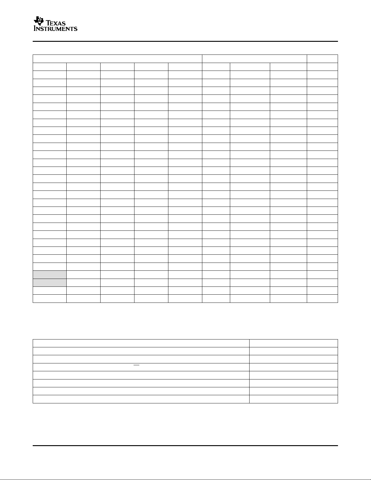
−160
−155
−150
−145
−140
−135
−130
−125
−120
−115
−110
VDD = 3.3 V
TA = 25°C
f = 622 MHz
÷1 Mode
Additive Phase Noise − dBc/Hz
f − Frequency Offset From Carrier − Hz
10 100 1k 100M10k 100k 10M1M
G001
−160
−155
−150
−145
−140
−135
−130
−125
−120
−115
−110
−105
−100
VDD = 3.3 V
TA = 25°C
f = 250 MHz
÷1 Mode
Additive Phase Noise − dBc/Hz
f − Frequency Offset From Carrier − Hz
10 100 1k 100M10k 100k 10M1M
G002
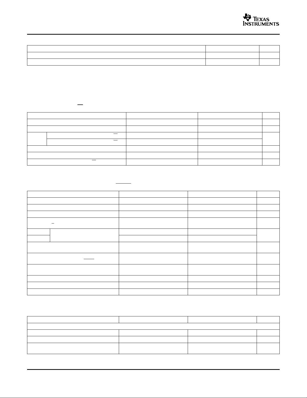
f − Frequency − GHz
0.40
0.45
0.50
0.55
0.60
0.65
0.70
0.75
0.80
0.85
0.90
0.1 0.3 0.5 0.7 0.9 1.1 1.3 1.5
LVPECL Output Swing − V
TA = 25°C
Load = 50 Ω to VDD − 2 V
VDD = 3.6 V
VDD = 3.3 V
VDD = 3 V
G003
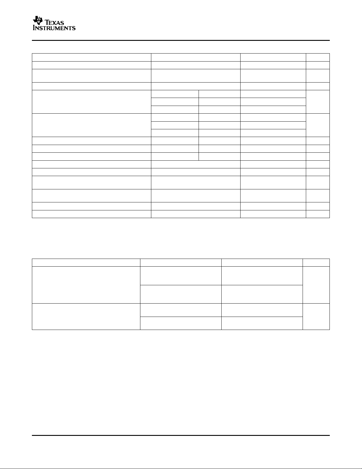
f − Frequency − MHz
0.0
0.5
1.0
1.5
2.0
2.5
3.0
3.5
25 75 125 175 225 275 325 375 425 475
LVCMOS Output Swing − V
TA = 25°C
Load = See Figure 10
VDD3 = 3 V
VDD3 = 3.6 V
VDD = 3.3 V
G004
CDCM1804
SCAS697E – JULY 2003 – REVISED MAY 2005
ADDITIVE PHASE NOISE ADDITIVE PHASE NOISE
vs vs
FREQUENCY OFFSET FROM CARRIER – LVPECL FREQUENCY OFFSET FROM CARRIER – LVCMOS
Figure 2. Figure 3.
LVPECL OUTPUT SWING LVCMOS OUTPUT SWING
vs vs
FREQUENCY FREQUENCY
8
Figure 4. Figure 5.
Page 9

www.ti.com
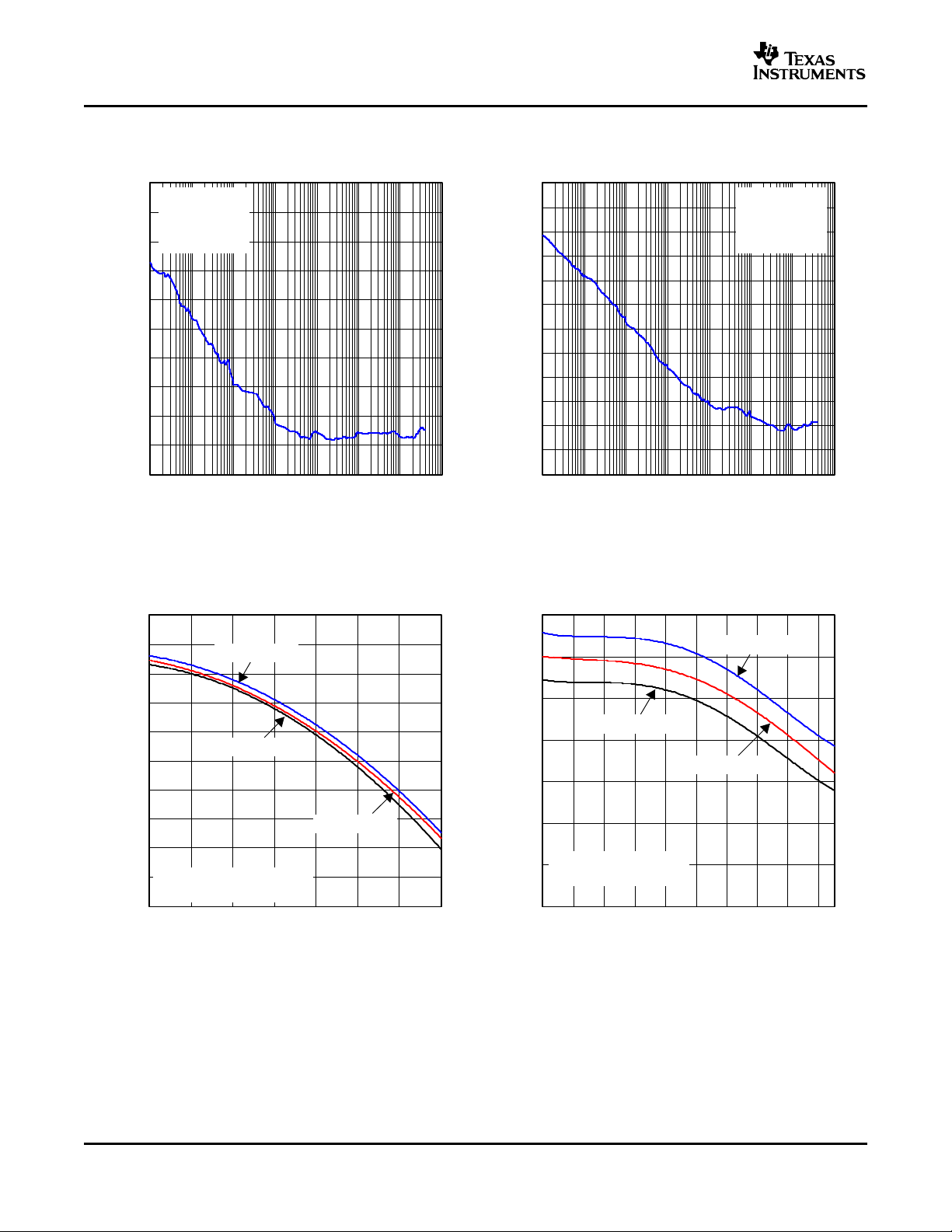
SUPPLY CURRENT ELECTRICAL CHARACTERISTICS
f − Frequency − MHz
110
120
130
140
150
160
170
180
100 300 500 700 900 1100 1300 1500
I
DD
− Supply Current − mA
VDD = 3.3 V
TA = 25°C
Load = 10 pF/1k/1k for LVCMOS
50 Ω to VDD − 2 V for LVPECL
3 LVPECL Outputs (÷1),
LVCMOS Output (÷4)
3 LVPECL Outputs (÷1)
Running, LVCMOS Output Off
2 LVPECL Outputs (÷1),
LVCMOS Output (÷4)
G005
over recommended operating free-air temperature range (unless otherwise noted)
PARAMETER TEST CONDITIONS MIN TYP MAX UNIT
All outputs enabled and terminated with 50 Ω to
V
– 2 V on LVPECL outputs and 10 pF on LVCMOS
Full load 160
Supply current mA
I
DD
No load 110
Supply current saving per LVPECL
output stage disabled, no load
I
Supply current, 3-state Hz, 0.5 mA
DDZ
DD
output, f = 800 MHz for LVPECL outputs and 200 MHz for
LVCMOS, V
= 3.3 V
DD
Outputs enabled, no output load, f = 800 MHz for LVPECL
outputs and 200 MHz for LVCMOS, V
f = 800 MHz for LVPECL output, V
All outputs in the high-impedance state by control logic, f = 0
V
= 3.6 V
DD
SUPPLY CURRENT
vs
FREQUENCY
SCAS697E – JULY 2003 – REVISED MAY 2005
= 3.6 V
DD
= 3.3 V 10 mA
DD
CDCM1804
Figure 6.
9
Page 10
www.ti.com
CDCM1804
SCAS697E – JULY 2003 – REVISED MAY 2005
PACKAGE THERMAL RESISTANCE
PARAMETER TEST CONDITIONS MIN TYP MAX UNIT
R
R
QFN-24 package thermal resistance
θ JA-1
QFN-24 package thermal resistance 4-layer JEDEC test board (JESD51-7) with four
with thermal vias in PCB
θ JA-2
(1)
(1) It is recommended to provide four thermal vias to connect the thermal pad of the package effectively with the PCB and ensure a good
heat sink.
Example:
Calculation of the junction-lead temperature with a 4-layer JEDEC test board using four thermal vias:
T
P
θ T
T
= 85 ° C (temperature of the chassis)
Chassis
= I
effective
Junction
Junction
max
= R
= θ T
T
die-max
Junction
= 125 ° C is not violated)
× V
θ JA-2
= 110 mA × 3.6 V = 396 mW (maximum power consumption inside the package)
max
× P
effective
+ T
Chassis
CONTROL INPUT CHARACTERISTICS
over recommended operating free-air temperature range
PARAMETER TEST CONDITIONS MIN TYP MAX UNIT
t
su
t
h
t
(disable)
t
(enable)
Rpullup Internal pullup resistor on S[2:0] and EN inputs 42 60 78 k Ω
V
IH(H)
V
IM(M)
V
IL(L)
I
IH
I
IL
(1) Leaving this terminal floating automatically pulls the logic level high to V
Setup time, S0, S1, S2, and EN terminals before clock IN 25 ns
Hold time, S0, S1, S2, and EN terminals after clock IN 0 ns
Time between latching the EN low transition and when all
outputs are disabled (how much time is required until the 10 ns
outputs turn off)
Time between latching the EN low-to-high transition and when
outputs are enabled based on control settings (how much time 1 µ s
passes before the outputs carry valid signals)
Three-level input high, S0, S1, S2, and EN terminals
Three-level input MID, S0, S1, S2, and EN terminals 0.3 V
Three-level input low, S0, S1, S2, and EN terminals 0.1 V
Input current, S0, S1, S2, and EN terminals
(1)
4-layer JEDEC test board (JESD51-7),
airflow = 0 ft/min
thermal vias of 22-mil diameter each, 55.4 ° C/W
airflow = 0 ft/min
= 55.45 ° C/W × 396 mW = 21.96 ° C
= 21.96 ° C + 85 ° C = 107 ° C (the maximum junction temperature of
(1)
VI= V
DD
VI= GND 38 85 µ A
through an internal pullup resistor of 60 k Ω .
DD
0.9 V
DD
DD
106.6 ° C/W
0.7 V
DD
DD
–5 µ A
V
V
V
BIAS VOLTAGE VBB
over recommended operating free-air temperature range
PARAMETER TEST CONDITIONS MIN TYP MAX UNIT
VBB Output reference voltage V
10
DD
= 3 V–3.6 V, IBB= –0.2 mA V
– 1.4 V
DD
DD
– 1.2 V
Page 11

www.ti.com
I − Load − mA
0.0
0.5
1.0
1.5
2.0
2.5
3.0
3.5
4.0
−5 0 5 10 15 20 25 30 35
VDD = 3.3 V
V
BB
− Output Reference Voltage − V
G006
OUTPUT REFERENCE VOLTAGE (VBB)
vs
LOAD
Figure 7.
CDCM1804
SCAS697E – JULY 2003 – REVISED MAY 2005
11
Page 12

www.ti.com
IN
IN
Y0
Y0
t
pd(LH1)
Y1
Y1
t
pd(LH2)
t
skLVCMOS(o)
Y3
0.5 × VDD3
Y2
Y2
NOTES: A. Output skew, t
sk(o)
, is calculated as the greater of:
− The difference between the fastest and the slowest t
pd(LH)n
(n = 0…2)
− The difference between the fastest and the slowest t
pd(HL)n
(n = 0…2)
B. Part-to-part skew, t
sk(pp)
, is calculated as the greater of:
− The difference between the fastest and the slowest t
pd(LH)n
(n = 0…2 for LVPECL, n = 3 for LVCMOS) across multiple devices
− The difference between the fastest and the slowest t
pd(HL)n
(n = 0…2 for LVPECL, n = 3 for LVCMOS) across multiple devices
C. Pulse skew, t
sk(p)
, is calculated as the magnitude of the absolute time difference between the high-to-low (t
pd(HL
) and the low-to-high
(t
pd(LH)
) propagation delays when a single switching input causes one or more outputs to switch, t
sk(p)
= | t
pd(HL)
− t
pd(LH)
|. Pulse skew
is sometimes referred to as pulse width distortion or duty cycle skew.
T0067-01
|YnYn|
Yn
Yn
V
OH
V
OL
80%
20%
0 V
t
r
t
f
V
OUT(pp)
T0058-02
CDCM1804
SCAS697E – JULY 2003 – REVISED MAY 2005
PARAMETER MEASUREMENT INFORMATION
12
Figure 8. Waveforms for Calculation of t
sk(o)
Figure 9. LVPECL Differential Output Voltage and Rise/Fall Time
and t
sk(pp)
Page 13

www.ti.com
LVCMOS
10 pF
Y3
CDCM1804
1 kΩ
1 kΩ
S0079-02
CDCM1804
SCAS697E – JULY 2003 – REVISED MAY 2005
PARAMETER MEASUREMENT INFORMATION (continued)
Figure 10. LVCMOS Output Loading During Device Test
PCB DESIGN FOR THERMAL FUNCTIONALITY
It is recommended to take special care of the PCB design for good thermal flow from the QFN-24 terminal
package to the PCB.
Due to the three LVPECL outputs, the current consumption of the CDCM1804 is fixed.
JEDEC JESD51-7 specifies thermal conductivity for standard PCB boards.
Modeling the CDCM1804 with a standard 4-layer JEDEC board results in a 67.22 ° C maximum temperature with
R
of 106.62 ° C/W for 25 ° C ambient temperature.
θ JA
When deploying four thermal vias (one per quadrant), the thermal flow improves significantly, yielding 46.94 ° C
maximum temperature with R
To ensure sufficient thermal flow, it is recommended to design with four thermal vias in applications enabling all
four outputs at once.
of 55.4 ° C/W for 25 ° C ambient temperature.
θ JA
13
Page 14

www.ti.com
Package Thermal Pad
(Underside)
Top Side
Island
Thermal Via
Dia 0.020 In.
Heat
Dissipation
VSS Copper Plane
VSS Copper Plane
M0029-01
CDCM1804
SCAS697E – JULY 2003 – REVISED MAY 2005
PARAMETER MEASUREMENT INFORMATION (continued)
Figure 11. Recommended Thermal Via Placement
See the application reports Quad Flatpack No-Lead Logic Packages (SCBA017 ) and QFN/SON PCB Attachment
(SLUA271 ) for further package-related information.
14
Page 15

www.ti.com
IN
150 Ω
150 Ω
C
AC
C
AC
50 Ω
50 Ω
IN
CDCM1804
C
VBB
50 Ω
50 Ω
S0085-01
LVPECL
LVPECL
130 Ω
83 Ω
CDCM1804
50 Ω
50 Ω
130 Ω
83 Ω
S0086-01
IN
IN
CDCM1804
SCAS697E – JULY 2003 – REVISED MAY 2005
APPLICATION INFORMATION
LVPECL RECEIVER INPUT TERMINATION
The input of the CDCM1804 has a high impedance and comes with a large common-mode voltage range.
For optimized noise performance, it is recommended to properly terminate the PCB trace (transmission line). If a
differential signal drives the CDCM1804, then a 100- Ω termination resistor is recommended to be placed as
close as possible across the input terminals. An even better approach is to install 2 × 50 Ω , with the center tap
connected to a capacitor (C) to terminate odd-mode noise and make up for transmission-line mismatches. The
VBB output can also be connected to the center tap to bias the input signal to (V
– 1.3 V) (see Figure 12 ).
DD
Figure 12. Recommended AC-Coupling LVPECL Receiver Input Termination
Figure 13. Recommended DC-Coupling LVPECL Receiver Input Termination
The CDCM1804 can also be driven by single-ended signals. Typically, the input signal becomes connected to
one input, while the complementary input must be properly biased to the center voltage of the incoming input
signal. For LVCMOS signals, this would be V
The best option (especially if the dc offset of the input signal might vary) is to ac-couple the input signal and then
/2, realized by a simple voltage divider (e.g., two 10-k Ω resistors).
CC
rebias the signal using the VBB reference output. See Figure 14 .
15
Page 16

www.ti.com
IN
CLK
C
AC
IN
CDCM1804
C
CT
VBB
R
dc
NOTE: CAC − AC-coupling capacitor (e.g., 10 nF)
CCT − Capacitor keeps voltage at IN constant (e.g., 10 nF)
Rdc − Load and correct duty cycle (e.g., 50 Ω)
VBB − Bias voltage output
S0087-01
CDCM1804
SCAS697E – JULY 2003 – REVISED MAY 2005
APPLICATION INFORMATION (continued)
Figure 14. Typical Application Setting for Single-Ended Input Signals Driving the CDCM1804
DEVICE BEHAVIOR DURING RESET AND CONTROL-TERMINAL SWITCHING
Output Behavior From Enabling the Device (EN = 0 → 1)
In disable mode (EN = 0), all output drivers are switched in high-Z mode. The S[2:0] control inputs are also
switched off. In the same mode, all flip-flops are reset. The typical current consumption is below 500 µ A.
When the device is enabled again, it takes typically 1 µ s for the settling of the reference voltage and currents.
During this time, the outputs Y[2:0] and Y[2:0] drive a high signal. Y3 is unknown (could be high or low). After the
settle time, the outputs go into the low state. Due to the synchronization of each output driver signal with the
input clock, the state of the waveforms after enabling the device is as shown in Figure 15 . The inverting input
and output signal are not included. The Y:/1 waveform is the undivided output driver state.
16
Page 17

www.ti.com
High-Z
EN
IN
Y:/1 Undefined
Low
High-ZY:/2 Undefined
Low
High-ZY:/4 Undefined
Low
1 µs
Signal State After the Device is Enabled (IN = Low)
High-Z
EN
IN
Y:/1 Undefined
Low
High-ZY:/2 Undefined
Low
High-ZY:/4 Undefined
Low
1 µs
Signal State After the Device is Enabled (IN = High)
Undivided State is Valid After the First
Positive Transition of the Input Clock
T0068-01
APPLICATION INFORMATION (continued)
CDCM1804
SCAS697E – JULY 2003 – REVISED MAY 2005
Enabling a Single Output Stage
If a single output stage becomes enabled:
• Y[2:0] is either low or high (undefined).
• Y[2:0] is the inverted signal of Y[2:0].
With the first positive clock transition, the undivided output becomes the input clock state. The divided output
states are equal to the actual internal divider. The internal divider is not reset while enabling single-output drivers.
Figure 15. Waveforms
17
Page 18

www.ti.com
High-Z
ENABLE Yx:
IN
Yx:/1
High-ZYx:/x Undefined
EnabledDisabled
Divider State
Undivided State is Valid After the First
Positive Transition of the Input Clock
Undefined
T0069-01
High-Z
ENABLE Yx:
IN
Yx:/1 Undefined
High-ZYx:/x Undefined Divider State
EnabledDisabled
Undivided State is Valid After the First
Positive Transition of the Input Clock
T0070-01
CDCM1804
SCAS697E – JULY 2003 – REVISED MAY 2005
APPLICATION INFORMATION (continued)
Figure 16. Signal State After an Output Driver Becomes Enabled While IN = 0
Figure 17. Signal State After an Output Driver Becomes Enabled While IN = 1
18
Page 19

Page 20

Page 21

Page 22

Page 23

PACKAGE OPTION ADDENDUM
www.ti.com
8-Aug-2005
PACKAGING INFORMATION
Orderable Device Status
(1)
Package
Type
Package
Drawing
Pins Package
Qty
Eco Plan
CDCM1804RGER ACTIVE QFN RGE 24 3000 Green (RoHS &
no Sb/Br)
CDCM1804RGERG4 ACTIVE QFN RGE 24 3000 Green (RoHS &
no Sb/Br)
CDCM1804RGET ACTIVE QFN RGE 24 250 Green (RoHS &
no Sb/Br)
CDCM1804RGETG4 ACTIVE QFN RGE 24 250 Green (RoHS &
no Sb/Br)
CDCM1804RTHR ACTIVE QFN RTH 24 3000 TBD CU SNPB Level-2-235C-1 YEAR
CDCM1804RTHT ACTIVE QFN RTH 24 250 TBD CU SNPB Level-2-235C-1 YEAR
(1)
The marketing status values are defined as follows:
ACTIVE: Product device recommended for new designs.
LIFEBUY: TI has announced that the device will be discontinued, and a lifetime-buy period is in effect.
NRND: Not recommended for new designs. Device is in production to support existing customers, but TI does not recommend using this part in
a new design.
PREVIEW: Device has been announced but is not in production. Samples may or may not be available.
OBSOLETE: TI has discontinued the production of the device.
(2)
Eco Plan - The planned eco-friendly classification: Pb-Free (RoHS) or Green (RoHS & no Sb/Br) - please check
http://www.ti.com/productcontent for the latest availability information and additional product content details.
TBD: The Pb-Free/Green conversion plan has not been defined.
Pb-Free (RoHS): TI's terms "Lead-Free" or "Pb-Free" mean semiconductor products that are compatible with the current RoHS requirements
for all 6 substances, including the requirement that lead not exceed 0.1% by weight in homogeneous materials. Where designed to be soldered
at high temperatures, TI Pb-Free products are suitable for use in specified lead-free processes.
Green (RoHS & no Sb/Br): TI defines "Green" to mean Pb-Free (RoHS compatible), and free of Bromine (Br) and Antimony (Sb) based flame
retardants (Br or Sb do not exceed 0.1% by weight in homogeneous material)
(2)
Lead/Ball Finish MSL Peak Temp
CU NIPDAU Level-2-260C-1 YEAR
CU NIPDAU Level-2-260C-1 YEAR
CU NIPDAU Level-2-260C-1 YEAR
CU NIPDAU Level-2-260C-1 YEAR
(3)
(3)
MSL, Peak Temp. -- The Moisture Sensitivity Level rating according to the JEDEC industry standard classifications, and peak solder
temperature.
Important Information and Disclaimer:The information provided on this page represents TI's knowledge and belief as of the date that it is
provided. TI bases its knowledge and belief on information provided by third parties, and makes no representation or warranty as to the
accuracy of such information. Efforts are underway to better integrate information from third parties. TI has taken and continues to take
reasonable steps to provide representative and accurate information but may not have conducted destructive testing or chemical analysis on
incoming materials and chemicals. TI and TI suppliers consider certain information to be proprietary, and thus CAS numbers and other limited
information may not be available for release.
In no event shall TI's liability arising out of such information exceed the total purchase price of the TI part(s) at issue in this document sold by TI
to Customer on an annual basis.
Addendum-Page 1
Page 24

IMPORTANT NOTICE
Texas Instruments Incorporated and its subsidiaries (TI) reserve the right to make corrections, modifications,
enhancements, improvements, and other changes to its products and services at any time and to discontinue
any product or service without notice. Customers should obtain the latest relevant information before placing
orders and should verify that such information is current and complete. All products are sold subject to TI’s terms
and conditions of sale supplied at the time of order acknowledgment.
TI warrants performance of its hardware products to the specifications applicable at the time of sale in
accordance with TI’s standard warranty. Testing and other quality control techniques are used to the extent TI
deems necessary to support this warranty . Except where mandated by government requirements, testing of all
parameters of each product is not necessarily performed.
TI assumes no liability for applications assistance or customer product design. Customers are responsible for
their products and applications using TI components. To minimize the risks associated with customer products
and applications, customers should provide adequate design and operating safeguards.
TI does not warrant or represent that any license, either express or implied, is granted under any TI patent right,
copyright, mask work right, or other TI intellectual property right relating to any combination, machine, or process
in which TI products or services are used. Information published by TI regarding third-party products or services
does not constitute a license from TI to use such products or services or a warranty or endorsement thereof.
Use of such information may require a license from a third party under the patents or other intellectual property
of the third party, or a license from TI under the patents or other intellectual property of TI.
Reproduction of information in TI data books or data sheets is permissible only if reproduction is without
alteration and is accompanied by all associated warranties, conditions, limitations, and notices. Reproduction
of this information with alteration is an unfair and deceptive business practice. TI is not responsible or liable for
such altered documentation.
Resale of TI products or services with statements different from or beyond the parameters stated by TI for that
product or service voids all express and any implied warranties for the associated TI product or service and
is an unfair and deceptive business practice. TI is not responsible or liable for any such statements.
Following are URLs where you can obtain information on other Texas Instruments products and application
solutions:
Products Applications
Amplifiers amplifier.ti.com Audio www.ti.com/audio
Data Converters dataconverter.ti.com Automotive www.ti.com/automotive
DSP dsp.ti.com Broadband www.ti.com/broadband
Interface interface.ti.com Digital Control www.ti.com/digitalcontrol
Logic logic.ti.com Military www.ti.com/military
Power Mgmt power.ti.com Optical Networking www.ti.com/opticalnetwork
Microcontrollers microcontroller.ti.com Security www.ti.com/security
Telephony www.ti.com/telephony
Video & Imaging www.ti.com/video
Wireless www.ti.com/wireless
Mailing Address: Texas Instruments
Post Office Box 655303 Dallas, Texas 75265
Copyright 2005, Texas Instruments Incorporated
 Loading...