

查询CDCF2510供应商
CDCF2510
3.3-V PHASE-LOCK LOOP CLOCK DRIVER
SCAS628B – APRIL 1999 REVISED NOVEMBER 1999
D
Designed to Meet PC133 SDRAM
Registered DIMM Specification Rev. 0.9
D
Spread Spectrum Clock Compatible
D
Operating Frequency 25 MHz to 140 MHz
D
Static tPhase Error Distribution at 66MHz to
133 MHz is ±125 ps
D
Jitter (cyc – cyc) at 66 MHz to 133 MHz Is
|70| ps
D
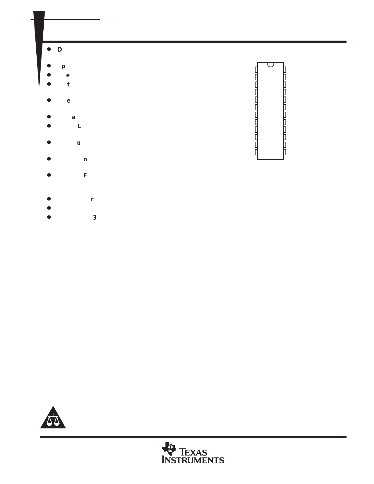
Available in Plastic 24-Pin TSSOP
D
Phase-Lock Loop Clock Distribution for
Synchronous DRAM Applications
D
Distributes One Clock Input to One Bank of
Ten Outputs
D
Output Enable Pin to Enable/Disable All 10
Outputs
D
External Feedback (FBIN) Terminal Is Used
to Synchronize the Outputs to the Clock
Input
D
On-Chip Series Damping Resistors
D
No External RC Network Required
D
Operates at 3.3 V
AGND
V
CC
1Y0
1Y1
1Y2
GND
GND
1Y3
1Y4
V
CC
FBOUT
PW PACKAGE
(TOP VIEW)
1
2
3
4
5
6
7
8
9
10
G
11
12
24
23
22
21
20
19
18
17
16
15
14
13
CLK
AV
CC
V
CC
1Y9
1Y8
GND
GND
1Y7
1Y6
1Y5
V
CC
FBIN
description
The CDCF2510 is a high-performance, low-skew, low-jitter, phase-lock loop (PLL) clock driver. It uses a PLL
to precisely align, in both frequency and phase, the feedback (FBOUT) output to the clock (CLK) input signal.
It is specifically designed for use with synchronous DRAMs. The CDCF2510 operates at 3.3 V VCC. It also
provides integrated series-damping resistors that make it ideal for driving point-to-point loads.
One bank of ten outputs provide ten low-skew, low-jitter copies of CLK. Output signal duty cycles are adjusted
to 50%, independent of the duty cycle at CLK. The outputs can be enabled/disabled with the control (G) input.
When the G input is high, the outputs switch in phase and frequency with CLK; when the G input is low, the
outputs are disabled to the logic-low state.
Unlike many products containing PLLs, the CDCF2510 does not require external RC networks. The loop filter
for the PLL is included on-chip, minimizing component count, board space, and cost.
Because it is based on PLL circuitry , the CDCF2510 requires a stabilization time to achieve phase lock of the
feedback signal to the reference signal. This stabilization time is required, following power up and application
of a fixed-frequency, fixed-phase signal at CLK, and following any changes to the PLL reference or feedback
signals. The PLL can be bypassed for test purposes by strapping AV
The CDCF2510 is characterized for operation from 0°C to 85°C.
For application information refer to application reports
CDC509/516/2509/2510/2516
Spectrum Clocking (SSC)
(literature number SLMA003) and
(literature number SCAA039).
High Speed Distribution Design Techniques for
to ground.
CC
Using CDC2509A/2510A PLL with Spread
Please be aware that an important notice concerning availability, standard warranty, and use in critical applications of
Texas Instruments semiconductor products and disclaimers thereto appears at the end of this data sheet.
PRODUCTION DATA information is current as of publication date.
Products conform to specifications per the terms of Texas Instruments
standard warranty. Production processing does not necessarily include
testing of all parameters.
POST OFFICE BOX 655303 • DALLAS, TEXAS 75265
Copyright 1999, Texas Instruments Incorporated
1
CDCF2510
3.3-V PHASE-LOCK LOOP CLOCK DRIVER
SCAS628B – APRIL 1999 REVISED NOVEMBER 1999
FUNCTION TABLE
INPUTS
G CLK
X L L L
L HLH
H H H H
functional block diagram
11
G
OUTPUTS
1Y
(0:9)
FBOUT
3
1Y0
4
1Y1
5
1Y2
CLK
FBIN
AV
CC
24
13
23
PLL
AVAILABLE OPTIONS
PACKAGE
T
A
0°C to 85°C CDCF2510PWR
SMALL OUTLINE
(PW)
15
16
17
20
21
12
8
9
1Y3
1Y4
1Y5
1Y6
1Y7
1Y8
1Y9
FBOUT
2
POST OFFICE BOX 655303 • DALLAS, TEXAS 75265
TYPE
DESCRIPTION
3.3-V PHASE-LOCK LOOP CLOCK DRIVER
SCAS628B – APRIL 1999 REVISED NOVEMBER 1999
Terminal Functions
TERMINAL
NAME NO.
Clock input. CLK provides the clock signal to be distributed by the CDCF2510 clock driver. CLK is used
to provide the reference signal to the integrated PLL that generates the clock output signals. CLK must
CLK 24 I
FBIN 13 I
G 11 I
FBOUT 12 O
3, 4, 5, 8, 9,
CC
15, 16, 17, 20,
21
23 Power
2, 10, 14, 22 Power Power supply
1Y (0:9)
AV
AGND 1 Ground Analog ground. AGND provides the ground reference for the analog circuitry.
V
CC
GND 6, 7, 18, 19 Ground Ground
have a fixed frequency and fixed phase for the PLL to obtain phase lock. Once the circuit is powered
up and a valid CLK signal is applied, a stabilization time is required for the PLL to phase lock the
feedback signal to its reference signal.
Feedback input. FBIN provides the feedback signal to the internal PLL. FBIN must be hard-wired to
FBOUT to complete the PLL. The integrated PLL synchronizes CLK and FBIN so that there is nominally
zero phase error between CLK and FBIN.
Output bank enable. G is the output enable for outputs 1Y(0:9). When G is low, outputs 1Y(0:9) are
disabled to a logic-low state. When G is high, all outputs 1Y(0:9) are enabled and switch at the same
frequency as CLK.
Feedback output. FBOUT is dedicated for external feedback. It switches at the same frequency as CLK.
When externally wired to FBIN, FBOUT completes the feedback loop of the PLL. FBOUT has an
integrated 25-Ω series-damping resistor .
Clock outputs. These outputs provide low-skew copies of CLK. Output bank 1Y(0:9) is enabled via the
G input. These outputs can be disabled to a logic-low state by deasserting the G control input. Each
O
output has an integrated 25-Ω series-damping resistor.
Analog power supply . AVCC provides the power reference for the analog circuitry. In addition, A VCC can
be used to bypass the PLL for test purposes. When AVCC is strapped to ground, PLL is bypassed and
CLK is buffered directly to the device outputs.
CDCF2510
POST OFFICE BOX 655303 • DALLAS, TEXAS 75265
3
CDCF2510
3.3-V PHASE-LOCK LOOP CLOCK DRIVER
SCAS628B – APRIL 1999 REVISED NOVEMBER 1999
absolute maximum ratings over operating free-air temperature range (unless otherwise noted)
Supply voltage range, AVCC (see Note 1) AVCC < VCC +0.7 V. . . . . . . . . . . . . . . . . . . . . . . . . . . . . . . . . . . . . . .
Supply voltage range, VCC –0.5 V to 4.6 V. . . . . . . . . . . . . . . . . . . . . . . . . . . . . . . . . . . . . . . . . . . . . . . . . . . . . . . . .
Input voltage range, V
(see Note 2) –0.5 V to 6.5 V. . . . . . . . . . . . . . . . . . . . . . . . . . . . . . . . . . . . . . . . . . . . . . . . .
I
Voltage range applied to any output in the high or low state,
VO (see Notes 2 and 3) –0.5 V to VCC + 0.5 V. . . . . . . . . . . . . . . . . . . . . . . . . . . . . . . . . . . . . . . . . . . . . . . . . . .
Input clamp current, I
Output clamp current, I
Continuous output current, I
(V
< 0) –50 mA. . . . . . . . . . . . . . . . . . . . . . . . . . . . . . . . . . . . . . . . . . . . . . . . . . . . . . . . . . .
IK
I
(V
< 0 or VO > VCC) ±50 mA. . . . . . . . . . . . . . . . . . . . . . . . . . . . . . . . . . . . . . . . . . . .
OK
O
(V
= 0 to VCC) ±50 mA. . . . . . . . . . . . . . . . . . . . . . . . . . . . . . . . . . . . . . . . . . . . . .
O
O
Continuous current through each VCC or GND ±100 mA. . . . . . . . . . . . . . . . . . . . . . . . . . . . . . . . . . . . . . . . . . . . .
Maximum power dissipation at TA = 55°C (in still air) (see Note 4) 0.7 W. . . . . . . . . . . . . . . . . . . . . . . . . . . . . . .
Storage temperature range, T
†
Stresses beyond those listed under “absolute maximum ratings” may cause permanent damage to the device. These are stress ratings only, and
functional operation of the device at these or any other conditions beyond those indicated under “recommended operating conditions” is not
implied. Exposure to absolute-maximum-rated conditions for extended periods may affect device reliability.
NOTES: 1. AVCC must not exceed VCC.
2. The input and output negative-voltage ratings may be exceeded if the input and output clamp-current ratings are observed.
3. This value is limited to 4.6 V maximum.
4. The maximum package power dissipation is calculated using a junction temperature of 150°C and a board trace length of 750 mils.
For more information, refer to the
Book
, literature number SCBD002.
–65°C to 150°C. . . . . . . . . . . . . . . . . . . . . . . . . . . . . . . . . . . . . . . . . . . . . . . . . . .
stg
Package Thermal Considerations
application note in the
ABT Advanced BiCMOS T echnology Data
recommended operating conditions (see Note 5)
MIN MAX UNIT
VCC, AVCCSupply voltage 3 3.6 V
V
IH
V
IL
V
I
I
OH
I
OL
T
A
NOTE 5: Unused inputs must be held high or low to prevent them from floating.
High-level input voltage 2 V
Low-level input voltage 0.8 V
Input voltage 0 V
High-level output current –12 mA
Low-level output current 12 mA
Operating free-air temperature 0 85 °C
CC
V
†
timing requirements over recommended ranges of supply voltage and operating free-air
temperature
MIN MAX UNIT
f
clk
†
Time required for the integrated PLL circuit to obtain phase lock of its feedback signal to its reference signal. For phase lock to be obtained, a
fixed-frequency , fixed-phase reference signal must be present at CLK. Until phase lock is obtained, the specifications for propagation delay, skew ,
and jitter parameters given in the switching characteristics table are not applicable. This parameter does not apply for input modulation under
SSC application.
4
Clock frequency 25 140 MHz
Input clock duty cycle 40% 60%
Stabilization time
†
POST OFFICE BOX 655303 • DALLAS, TEXAS 75265
1 ms

(INPUT)/CONDITION
(OUTPUT)
Clkin
133 MH
ps
(cycle cycle)
CDCF2510
3.3-V PHASE-LOCK LOOP CLOCK DRIVER
SCAS628B – APRIL 1999 REVISED NOVEMBER 1999
electrical characteristics over recommended operating free-air temperature range (unless
otherwise noted)
PARAMETER TEST CONDITIONS VCC, AV
V
IK
V
OH
V
OL
I
OH
I
OL
I
I
I
CC
∆I
C
C
‡
For conditions shown as MIN or MAX, use the appropriate value specified under recommended operating conditions.
§
For ICC of AVCC, and ICC vs Frequency (see Figures 8 and 9).
Input clamp voltage II = –18 mA 3 V –1.2 V
IOH = –100 µA MIN to MAX VCC–0.2
High-level output voltage
Low-level output voltage
High-level output current
Low-level output current
Input current VI = VCC or GND 3.6 V ±5 µA
§
Supply current
Change in supply current
CC
Input capacitance VI = VCC or GND 3.3 V 4 pF
i
Output capacitance VO = VCC or GND 3.3 V 6 pF
o
IOH = –12 mA 3 V 2.1
IOH = –6 mA 3 V 2.4
IOL = 100 µA MIN to MAX 0.2
IOL = 12 mA 3 V 0.8
IOL = 6 mA 3 V 0.55
VO = 1 V 3.135 V –32
VO = 1.65 V 3.3 V –36
VO = 3.135 V 3.465 V –12
VO = 1.95 V 3.135 V 34
VO = 1.65 V 3.3 V 40
VO = 0.4 V 3.465 V 14
VI = VCC or GND,
Outputs: low or high
One input at VCC – 0.6 V,
Other inputs at VCC or GND
IO = 0,
3.3 V to 3.6 V 500 µA
CC
3.6 V 10 µA
MIN TYP‡MAX UNIT
V
V
switching characteristics over recommended ranges of supply voltage and operating free-air
temperature, C
Phase error time – static (normalized)
(See Figures 3 – 6)
t
sk(o)
t
r
t
f
‡
These parameters are not production tested.
§
The t
NOTES: 6. The specifications for parameters in this table are applicable only after any appropriate stabilization time has elapsed.
Intel is a trademark of Intel Corporation.
PC SDRAM Register DIMM Design Support Document is published by Intel Corporation.
Output skew time
Phase error time – jitter (see Note 7)
Jitter
(See Figure 7)
Duty cycle F(clkin > 60 MHz) Any Y or FBOUT 45% 55%
Rise time (See Notes 8 and 9)
Fall time (See Notes 8 and 9)
specification is only valid for equal loading of all outputs.
sk(o)
7. Calculated per PC DRAM SPEC (t
8. This is equivalent to 0.8 ns/2.5 ns and 0.8 ns/2.7 ns into standard 500 Ω/ 30 pf load for output swing of 04. V to 2 V.
9. 64 MB DIMM configuration according to PC SDRAM Registered DIMM Design Support Document, Figure 20 and Table 13.
= 25 pF (see Note 6 and Figures 1 and 2)
L
PARAMETER
§
-
CLKIN↑ = 66 MHz to133 MHz FBIN↑ –125 125 ps
Clkin = 100 MHz to 133 MHz
phase error
FROM
Any Y or FBOUT Any Y or FBOUT 200 ps
= 66 MHz to
VO = 1.2 V to 1.8 V,
IBIS simulation
VO = 1.2 V to 1.8 V,
IBIS simulation
, static – jitter
(cycle-to-cycle)
‡
TO
Any Y or FBOUT –50 50
z
Any Y or FBOUT |70|
Any Y or FBOUT |65| ps
Any Y or FBOUT 2.5 1 V/ns
Any Y or FBOUT 2.5 1 V/ns
).
VCC, AVCC = 3.3 V
± 0.3 V
MIN TYP MAX
UNIT
p
POST OFFICE BOX 655303 • DALLAS, TEXAS 75265
5

CDCF2510
3.3-V PHASE-LOCK LOOP CLOCK DRIVER
SCAS628B – APRIL 1999 REVISED NOVEMBER 1999
PARAMETER MEASUREMENT INFORMATION
From Output
Under Test
500
25 pF
W
Input
Output
3 V
50% V
CC
t
pd
t
r
0.4 V
2 V
50% V
CC
2 V
t
f
0.4 V
0 V
V
V
OH
OL
LOAD CIRCUIT FOR OUTPUTS
NOTES: A. CL includes probe and jig capacitance.
B. All input pulses are supplied by generators having the following characteristics: PRR ≤ 133 MHz, ZO = 50 Ω, tr ≤ 1.2 ns, tf≤ 1.2 ns.
C. The outputs are measured one at a time with one transition per measurement.
Figure 1. Load Circuit and Voltage Waveforms
CLKIN
FBIN
t
phase error
FBOUT
Any Y
t
sk(o)
VOLTAGE WAVEFORMS
PROPAGATION DELAY TIMES
Any Y
Any Y
t
sk(o)
Figure 2. Phase Error and Skew Calculations
6
POST OFFICE BOX 655303 • DALLAS, TEXAS 75265
CDCF2510
3.3-V PHASE-LOCK LOOP CLOCK DRIVER
SCAS628B – APRIL 1999 REVISED NOVEMBER 1999
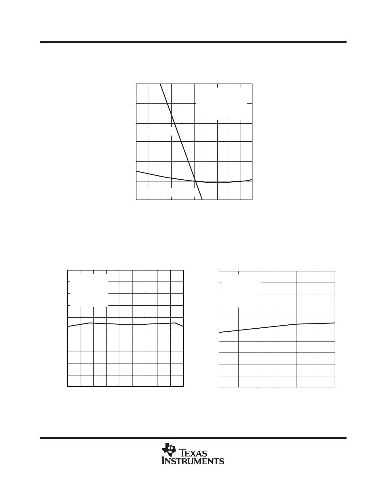
TYPICAL CHARACTERISTICS
PHASE ADJUSTMENT SLOPE AND PHASE ERROR
vs
LOAD CAPACITANCE
20
10
0
Phase Error
VCC = 3.3 V
fc = 133 MHz
C
= 25pF
(LY)
TA = 25°C
See Notes A and B
200
100
0
–10
–20
Phase Adjustment Slope – ps/pF
–30
Phase Adjustment Slope
–40
0 5 10 15 20 25 30 35 40
C
– Lumped Feedback Capacitance at FBIN – pF
(LF)
–100
–200
–300
–400
45 50
Figure 3
NOTES: A. Trace feedback length FBOUT to FBIN = 5 mm, ZO = 50 Ω Phase error measured from CLK to Y
B. CLF = Lumped feedback capacitance at FBIN
PHASE ERROR
vs
CLOCK FREQUENCY
0
VCC = 3.3 V
–50
C
= 25 pF
(LY)
C
= 12 pF
–100
–150
–200
(LF)
TA = 25°C
See Note A
–50
–100
–150
–200
0
fc = 133 MHz
C
C
TA = 25°C
See Note A
(LY)
(LF)
PHASE ERROR
SUPPLY VOLTAGE
= 25 pF
= 12 pF
Phase Error – ps
vs
–250
–300
Phase Error – ps
–350
–400
–450
–500
50 60 70 80 90 100 110 120
fc – Clock Frequency – MHz
130 140
Figure 4
NOTE A: Trace feedback length FBOUT to FBIN = 5 mm, ZO = 50 Ω
POST OFFICE BOX 655303 • DALLAS, TEXAS 75265
–250
–300
Phase Error – ps
–350
–400
–450
–500
3.1 3.2 3.3 3.4 3.5
VCC – Supply Voltage – V
Figure 5
3.63
7

CDCF2510
3.3-V PHASE-LOCK LOOP CLOCK DRIVER
SCAS628B – APRIL 1999 REVISED NOVEMBER 1999
TYPICAL CHARACTERISTICS
STATIC PHASE ERROR
vs
CLOCK FREQUENCY
0
VCC = 3.3 V
–50
C
= 25 pF
(LY)
C
= 12 pF
–100
–150
–200
–250
–300
Phase Error – ps
–350
–400
–450
–500
(LF)
TA = 25°C
See Note A
50 60 70 80 90 100 110 120
fc – Clock Frequency – MHz
130 140
Figure 6
NOTES: A. Trace feedback length FBOUT to FBIN = 5 mm, ZO = 50 Ω
B. Phase error measured from CLK to FBIN
C. CLY = Lumped capacitive load at Y
D. CLF = Lumped feedback capacitance at FBIN
JITTER
vs
CLOCK FREQUENCY
300
250
200
150
Jitter – ps
100
50
Cycle to Cycle
0
50 60 70 80 90 100 110 120 130 140
fc – Clock Frequency – MHz
VCC = 3.3 V
C
= 25 pF
(LY)
C
= 12 pF
(LF)
TA = 25°C
See Notes A and B
Peak to Peak
Figure 7
8
POST OFFICE BOX 655303 • DALLAS, TEXAS 75265

CDCF2510
3.3-V PHASE-LOCK LOOP CLOCK DRIVER
SCAS628B – APRIL 1999 REVISED NOVEMBER 1999
TYPICAL CHARACTERISTICS
ANALOG SUPPLY CURRENT
16
AVCC = VCC = 3.465 V
14
Bias = 0/3 V
C
= 25 pf
(LY)
C
= 0
(LF)
12
TA = 25°C
See Notes A and B
10
8
6
– Analog Supply Current – mA
4
CC
AI
2
0
10 30 50 70 90 110 130 150
fc – Clock Frequency – MHz
NOTES: A. C
B. C
= Lumped capacitive load at Y
(LY)
= Lumped feedback capacitance at FBIN
(LF)
vs
CLOCK FREQUENCY
Figure 8
SUPPLY CURRENT
vs
CLOCK FREQUENCY
300
AVCC = VCC = 3.465 V
Bias = 0/3 V
C
250
200
150
– Supply Current – mA
100
CC
I
50
0
10 30 50 70 90 110 130 150
= 25 pf
(LY)
C
= 0
(LF)
TA = 25°C
See Notes A and B
fc – Clock Frequency – MHz
Figure 9
POST OFFICE BOX 655303 • DALLAS, TEXAS 75265
9

CDCF2510
3.3-V PHASE-LOCK LOOP CLOCK DRIVER
SCAS628B – APRIL 1999 REVISED NOVEMBER 1999
MECHANICAL INFORMATION
PW (R-PDSO-G**) PLASTIC SMALL-OUTLINE PACKAGE
14 PIN SHOWN
0,65
14
1
1,20 MAX
A
7
0,05 MIN
0,30
0,19
8
6,60
4,50
4,30
6,20
M
0,10
Seating Plane
0,10
0,15 NOM
Gage Plane
0,25
0°–8°
0,75
0,50
PINS **
DIM
A MAX
A MIN
NOTES: A. All linear dimensions are in millimeters.
B. This drawing is subject to change without notice.
C. Body dimensions do not include mold flash or protrusion not to exceed 0,15.
D. Falls within JEDEC MO-153
8
3,10
2,90
14
5,10
4,90
16
5,10
20
6,60
6,404,90
24
7,90
7,70
28
9,80
9,60
4040064/E 08/96
10
POST OFFICE BOX 655303 • DALLAS, TEXAS 75265

IMPORTANT NOTICE
T exas Instruments and its subsidiaries (TI) reserve the right to make changes to their products or to discontinue
any product or service without notice, and advise customers to obtain the latest version of relevant information
to verify, before placing orders, that information being relied on is current and complete. All products are sold
subject to the terms and conditions of sale supplied at the time of order acknowledgement, including those
pertaining to warranty, patent infringement, and limitation of liability.
TI warrants performance of its semiconductor products to the specifications applicable at the time of sale in
accordance with TI’s standard warranty. Testing and other quality control techniques are utilized to the extent
TI deems necessary to support this warranty . Specific testing of all parameters of each device is not necessarily
performed, except those mandated by government requirements.
CERTAIN APPLICATIONS USING SEMICONDUCTOR PRODUCTS MAY INVOLVE POTENTIAL RISKS OF
DEATH, PERSONAL INJURY, OR SEVERE PROPERTY OR ENVIRONMENTAL DAMAGE (“CRITICAL
APPLICATIONS”). TI SEMICONDUCTOR PRODUCTS ARE NOT DESIGNED, AUTHORIZED, OR
WARRANTED TO BE SUITABLE FOR USE IN LIFE-SUPPORT DEVICES OR SYSTEMS OR OTHER
CRITICAL APPLICA TIONS. INCLUSION OF TI PRODUCTS IN SUCH APPLICATIONS IS UNDERST OOD TO
BE FULLY AT THE CUSTOMER’S RISK.
In order to minimize risks associated with the customer’s applications, adequate design and operating
safeguards must be provided by the customer to minimize inherent or procedural hazards.
TI assumes no liability for applications assistance or customer product design. TI does not warrant or represent
that any license, either express or implied, is granted under any patent right, copyright, mask work right, or other
intellectual property right of TI covering or relating to any combination, machine, or process in which such
semiconductor products or services might be or are used. TI’s publication of information regarding any third
party’s products or services does not constitute TI’s approval, warranty or endorsement thereof.
Copyright 2000, Texas Instruments Incorporated
 Loading...