

www.DataSheet4U.com
Data sheet acquired from Harris Semiconductor
[
(
C
C
C
/
(
S
C
L
4
i
SCHS195C
January 1998 - Revised October 2003
CD54HC670, CD74HC670,
CD74HCT670
High-Speed CMOS Logic
4x4 Register File
/Title
CD74H
670,
D74H
T670)
Subject
High-
peed
MOS
ogic
x4 Reg-
ster
Features
• Simultaneous and Independent Read and Write
Operations
• Expandable to 512 Words of n-Bits
• Three-State Outputs
• Organized as 4 Words x 4 Bits Wide
• Buffered Inputs
• Typical Read Time = 16ns for ’HC670 V
15pF, T
• Fanout (Over Temperature Range)
- Standard Outputs. . . . . . . . . . . . . . . 10 LSTTL Loads
- Bus Driver Outputs . . . . . . . . . . . . . 15 LSTTL Loads
• Wide Operating Temperature Range . . . -55
• Balanced Propagation Delay and Transition Times
• Significant Power Reduction Compared to LSTTL
Logic ICs
• HC Types
- 2V to 6V Operation
- High Noise Immunity: N
• HCT Types
- 4.5V to 5.5V Operation
- Direct LSTTL Input Logic Compatibility,
- CMOS Input Compatibility, I
= 25oC
A
at VCC = 5V
V
= 0.8V (Max), VIH = 2V (Min)
IL
= 30%, NIH = 30% of V
IL
≤ 1µA at VOL, V
l
= 5V, CL =
CC
o
C to 125oC
OH
Description
The ’HC670 and CD74HCT670 are 16-bit register files
organized as 4 words x 4 bits each. Read and write address
and enableinputs allow simultaneouswritinginto one location
while reading another. Four data inputs are provided to store
the 4-bit word. The write address inputs (WA0 and WA1)
determine the location of the stored word in the register.
When write enable (
address location and it remains transparent to the data. The
outputs will reflect the true form of the input data. When (
is high data and address inputs are inhibited. Data acquisition
from the four registers is made possible by the read address
inputs (RA1 and RA0). The addressed word appears at the
output when the read enable (
high impedance state when the (
tied together to increase the word capacity to 512 x 4 bits.
WE) is low the word is entered into the
RE) is low. The output is in the
RE) is high. Outputs can be
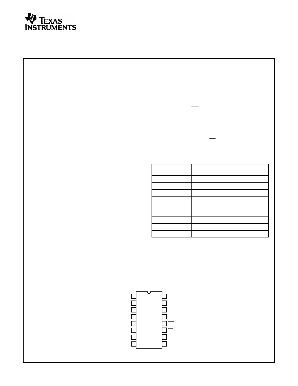
Ordering Information
TEMP. RANGE
PART NUMBER
CD54HC670F3A -55 to 125 16 Ld CERDIP
CD74HC670E -55 to 125 16 Ld PDIP
CD74HC670M -55 to 125 16 Ld SOIC
CC
CD74HC670MT -55 to 125 16 Ld SOIC
CD74HC670M96 -55 to 125 16 Ld SOIC
CD74HCT670E -55 to 125 16 Ld PDIP
CD74HCT670M -55 to 125 16 Ld SOIC
CD74HCT670MT -55 to 125 16 Ld SOIC
CD74HCT670M96 -55 to 125 16 Ld SOIC
NOTE: When ordering, use the entire part number. The suffix 96
denotes tape and reel. The suffix T denotes a small-quantity reel of
250.
(oC) PACKAGE
WE)
Pinout
CD54HC670
(CERDIP)
CD74HC670, CD74HCT670
(PDIP, SOIC)
TOP VIEW
16
1
D1
2
D2
3
D3
4
RA1
5
RA0
6
Q3
7
Q2
8
GND
CAUTION: These devices are sensitive to electrostatic discharge. Users should follow proper IC Handling Procedures.
Copyright
© 2003, Texas Instruments Incorporated
1
V
CC
15
D0
14
WA0
13
WA1
12
WE
11
RE
10
Q0
9
Q1
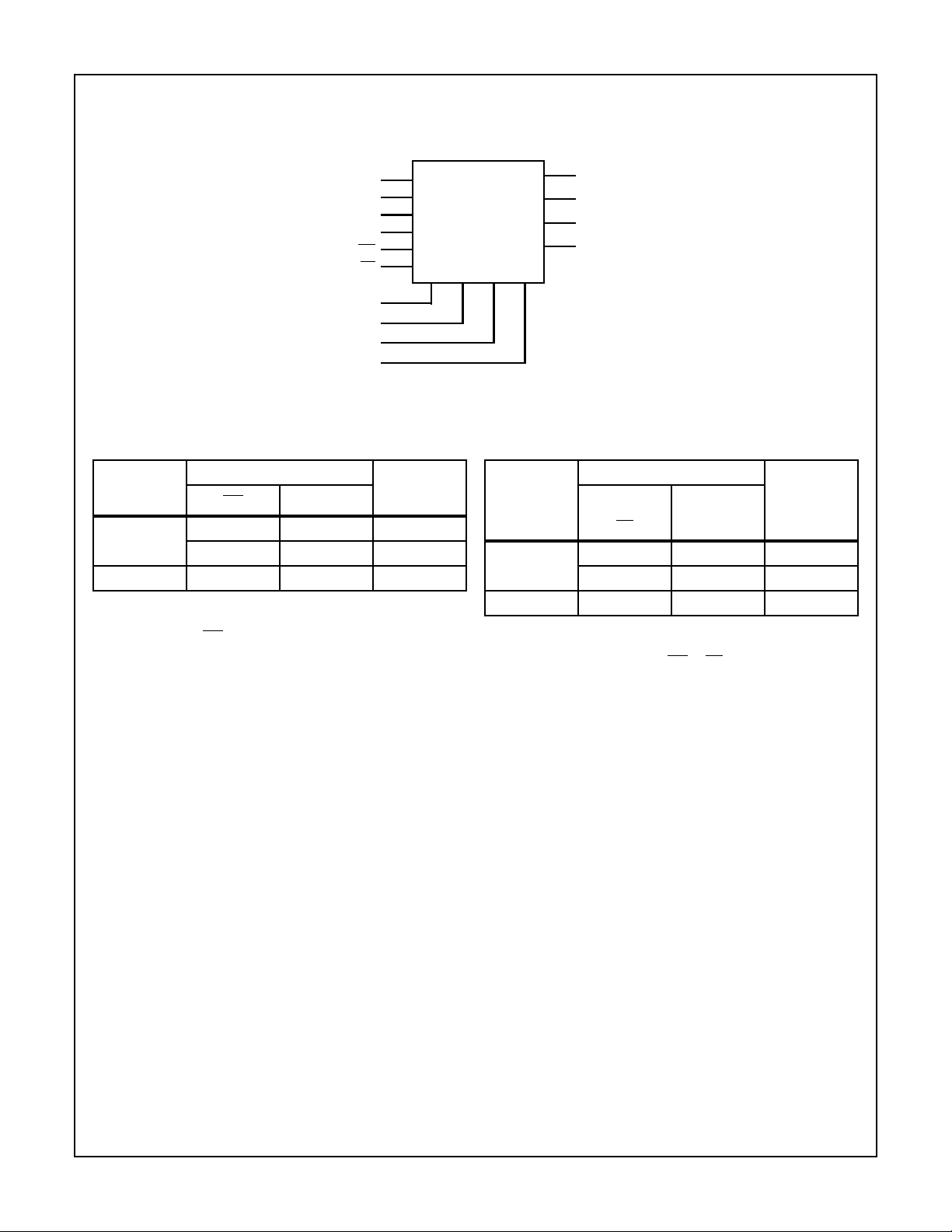
Functional Diagram
CD54HC670, CD74HC670, CD74HCT670CD54HC670, CD74HC670, CD74HCT670
15
D0
1
D1
2
D2
3
D3
12
WE
11
RE
RA1
RA0
WA0
WA1
4
WRITE MODE SELECT TABLE
INPUTS INTERNAL
OPERATING
MODE
N
LATCHES
(NOTE 1)WE D
Write Data L L L
LHH
Data Latched H X No Change
NOTE:
1. The Write Address (WA0 andWA1) to the “internal latches”must
be stable while WE is LOW for conventional operation.
10
Q0
9
Q1
7
Q2
6
Q3
514 13
READ MODE SELECT TABLE
INPUTS
INTERNAL
OPERATING
MODE
RE
LATCHES
(NOTE 2)
Read L L L
LHH
Disabled H X (Z)
NOTE:
2. The selection ofthe“internal latches” byReadAddress (RA0 and
RA1) are not constrained by WE or RE operation.
H = High Voltage Level
L = Low Voltage Level
X= Don’t Care
Z = High Impedance “Off” State
OUTPUT
Q
N
2
CD54HC670, CD74HC670, CD74HCT670CD54HC670, CD74HC670, CD74HCT670
Absolute Maximum Ratings Thermal Information
DC Supply Voltage, VCC. . . . . . . . . . . . . . . . . . . . . . . . -0.5V to 7V
DC Input Diode Current, I
IK
For VI < -0.5V or VI > VCC + 0.5V. . . . . . . . . . . . . . . . . . . . . .±20mA
DC Output Diode Current, I
OK
For VO < -0.5V or VO > VCC + 0.5V . . . . . . . . . . . . . . . . . . . .±20mA
DC Drain Current, per Output, I
O
For -0.5V < VO < VCC + 0.5V. . . . . . . . . . . . . . . . . . . . . . . . . .±35mA
DC Output Source or Sink Current per Output Pin, I
O
For VO > -0.5V or VO < VCC + 0.5V . . . . . . . . . . . . . . . . . . . .±25mA
DC VCC or Ground Current, ICC . . . . . . . . . . . . . . . . . . . . . . . . .±50mA
Operating Conditions
Temperature Range, TA . . . . . . . . . . . . . . . . . . . . . . -55oC to 125oC
Supply Voltage Range, V
HC Types . . . . . . . . . . . . . . . . . . . . . . . . . . . . . . . . . . . . .2V to 6V
HCT Types . . . . . . . . . . . . . . . . . . . . . . . . . . . . . . . . .4.5V to 5.5V
DC Input or Output Voltage, VI, VO . . . . . . . . . . . . . . . . . 0V to V
Input Rise and Fall Time
2V . . . . . . . . . . . . . . . . . . . . . . . . . . . . . . . . . . . . . . 1000ns (Max)
4.5V. . . . . . . . . . . . . . . . . . . . . . . . . . . . . . . . . . . . . . 500ns (Max)
6V . . . . . . . . . . . . . . . . . . . . . . . . . . . . . . . . . . . . . . . 400ns (Max)
CAUTION: Stresses above those listed in “Absolute Maximum Ratings” may cause permanent damage to the device. This is a stress only rating and operation
of the device at these or any other conditions above those indicated in the operational sections of this specification is not implied.
NOTE:
3. The package thermal impedance is calculated in accordance with JESD 51-7.
CC
Thermal Resistance (Typical, Note 3) θJA (oC/W)
E (PDIP) Package . . . . . . . . . . . . . . . . . . . . . . . . . . 67
M (SOIC) Package. . . . . . . . . . . . . . . . . . . . . . . . . . 73
Maximum Junction Temperature. . . . . . . . . . . . . . . . . . . . . . .150oC
Maximum Storage Temperature Range . . . . . . . . . .-65oC to 150oC
Maximum Lead Temperature (Soldering 10s). . . . . . . . . . . . .300oC
(SOIC - Lead Tips Only)
CC
DC Electrical Specifications
PARAMETER SYMBOL
HC TYPES
High Level Input
Voltage
Low Level Input
Voltage
High Level Output
Voltage
CMOS Loads
High Level Output
Voltage
TTL Loads
Low Level Output
Voltage
CMOS Loads
Low Level Output
Voltage
TTL Loads
Input Leakage
Current
V
IH
V
IL
V
OH
V
OL
I
I
TEST
CONDITIONS
(V) IO(mA) MIN TYP MAX MIN MAX MIN MAX
I
V
CC
(V)
o
C -40oC TO 85oC -55oC TO 125oC
25
UNITSV
- - 2 1.5 - - 1.5 - 1.5 - V
4.5 3.15 - - 3.15 - 3.15 - V
6 4.2 - - 4.2 - 4.2 - V
- - 2 - - 0.5 - 0.5 - 0.5 V
4.5 - - 1.35 - 1.35 - 1.35 V
6 - - 1.8 - 1.8 - 1.8 V
VIHor VIL-0.02 2 1.9 - - 1.9 - 1.9 - V
-0.02 4.5 4.4 - - 4.4 - 4.4 - V
-0.02 6 5.9 - - 5.9 - 5.9 - V
- - ---- - - - V
-6 4.5 3.98 - - 3.84 - 3.7 - V
-7.8 6 5.48 - - 5.34 - 5.2 - V
VIHor VIL0.02 2 - - 0.1 - 0.1 - 0.1 V
0.02 4.5 - - 0.1 - 0.1 - 0.1 V
0.02 6 - - 0.1 - 0.1 - 0.1 V
- - ---- - - - V
6 4.5 - - 0.26 - 0.33 - 0.4 V
7.8 6 - - 0.26 - 0.33 - 0.4 V
VCC or
-6--±0.1 - ±1-±1 µA
GND
3
CD54HC670, CD74HC670, CD74HCT670CD54HC670, CD74HC670, CD74HCT670
DC Electrical Specifications (Continued)
TEST
CONDITIONS
PARAMETER SYMBOL
Quiescent Device
I
CC
Current
Three-State Leakage
Current
HCT TYPES
High Level Input
Voltage
Low Level Input
Voltage
High Level Output
Voltage
V
IH
V
IL
V
OH
CMOS Loads
High Level Output
Voltage
TTL Loads
Low Level Output
V
OL
Voltage
CMOS Loads
Low Level Output
Voltage
TTL Loads
Input Leakage
Current
Quiescent Device
Current
I
I
I
CC
Three-State Leakage
Current
Additional Quiescent
Device Current Per
∆I
CC
(Note 4)
Input Pin: 1 Unit Load
NOTE:
4. For dual-supply systems theoretical worst case (V
(V) IO(mA) MIN TYP MAX MIN MAX MIN MAX
I
VCC or
GND
or VIHVO =
V
IL
VCC or
GND
- - 4.5 to
- - 4.5 to
VIHor VIL-0.02 4.5 4.4 - - 4.4 - 4.4 - V
VIHor VIL0.02 4.5 - - 0.1 - 0.1 - 0.1 V
VCCand
GND
VCC or
GND
or VIHVO =
V
IL
VCC or
GND
V
CC
-2.1
o
C -40oC TO 85oC -55oC TO 125oC
V
CC
(V)
25
UNITSV
0 6 - - 8 - 80 - 160 µA
6--±0.5 - ±5.0 - ±10 µA
2--2- 2 - V
5.5
- - 0.8 - 0.8 - 0.8 V
5.5
-6 4.5 3.98 - - 3.84 - 3.7 - V
6 4.5 - - 0.26 - 0.33 - 0.4 V
0 5.5 - ±0.1 - ±1-±1 µA
0 5.5 - - 8 - 80 - 160 µA
5.5 - - ±0.5 - ±5.0 - ±10 µA
- 4.5 to
- 100 360 - 450 - 490 µA
5.5
= 2.4V, VCC = 5.5V) specification is 1.8mA.
I
HCT Input Loading Table
INPUT UNIT LOADS
WE 0.3
WA0 0.2
WA1 0.4
RE 1.5
DATA 0.15
RA0 0.4
RA1 0.7
NOTE: UnitLoad is∆ICClimitspecific in DC Electrical Specifications
Table, e.g., 360µA max. at 25oC.
4
CD54HC670, CD74HC670, CD74HCT670CD54HC670, CD74HC670, CD74HCT670
Prerequisite for Switching Specifications
25oC -40oC TO 85oC -55oC TO 125oC
PARAMETER SYMBOL VCC(V)
HC TYPES
Setup Time
tSU, t
h
Data to WE
Write to WE
Hold Time
tH, t
W
Data to WE
Write to WE
Pulse Width WE t
Latch Time WE to RA0,
W
t
LATCH
RA1
HCT TYPES
Setup Time
tSU, t
h
Data to WE
UNITSMIN TYP MAX MIN TYP MAX MIN TYP MAX
260- -75- -90--ns
4.5 12 - - 15 - - 18 - - ns
610- -13- -15--ns
25--5--5--ns
4.5 5 - - 5 - - 5 - - ns
65--5--5--ns
2 80 - - 100 - - 120 - - ns
4.5 16 - - 20 - - 24 - - ns
614- -17- -20--ns
2 100 - - 125 - - 150 - - ns
4.5 20 - - 25 - - 30 - - ns
617- -21- -26--ns
4.5 12 - - 15 - - 18 - - ns
Hold Time
tH, t
W
4.5 5 - - 5 - - 5 - - ns
Data to WE
Write to WE
Setup Time
t
SU
4.5 18 - - 23 - - 27 - - ns
Write to WE
Pulse Width WE t
Latch Time WE to RA0,
t
LATCH
W
4.5 20 - - 25 - - 30 - - ns
4.5 25 - - 31 - - 38 - - ns
RA1
Switching Specifications C
PARAMETER SYMBOL
= 50pF, Input tr, tf= 6ns
L
TEST
CONDITIONS VCC(V)
25oC
-40oC TO
85oC
-55oC TO
125oC
HC TYPES
Propagation Delay t
PLH
, t
PHLCL
= 50pF
Reading Any Word 2 - - 195 - 245 - 295 ns
4.5 - - 39 - 49 - 59 ns
CL = 15pF 5 - 16 - - - - - ns
CL = 50pF 6 - - 33 - 42 - 50 ns
Write Enable to Output t
PLH,tPHLCL
= 50pF 2 - - 250 - 315 - 375 ns
4.5 - - 50 - 63 - 75 ns
CL = 15pF 5 - 21 - - - - - ns
CL = 50pF 6 - - 43 - 54 - 64 ns
UNITSMIN TYP MAX MIN MAX MIN MAX
5

CD54HC670, CD74HC670, CD74HCT670
Switching Specifications C
PARAMETER SYMBOL
Data to Output t
= 50pF, Input tr, tf= 6ns (Continued)
L
TEST
CONDITIONS VCC(V)
PLH,tPHLCL
= 50pF 2 - - 256 - 315 - 375 ns
25oC
-40oC TO
85oC
-55oC TO
125oC
4.5 - - 50 - 63 - 75 ns
CL = 15pF 5 - 21 - - - - - ns
CL = 50pF 6 - - 43 - 54 - 64 ns
Output Disable Time t
PLZ,tPHZ
CL = 50pF 2 - - 150 - 190 - 225 ns
4.5 - - 30 - 38 - 45 ns
CL = 15pF 5 - 12 - - - - - ns
CL = 50pF 6 - - 26 - 33 - 38 ns
Output Enable Time t
PZL,tPZH
CL = 50pF 2 - - 150 - 190 - 225 ns
4.5 - - 30 - 38 - 45 ns
CL = 15pF 5 - 12 - - - - - ns
CL = 50pF 6 - - 26 - 33 - 38 ns
Output Transition Time t
THL
, t
CL = 50pF 2 - - 75 - 95 - 110 ns
TLH
4.5 - - 15 - 19 - 22 ns
6 - - 13 - 10 - 19 ns
Input Capacitance C
Three-State Output
I
C
O
CL = 50pF - 10 - 10 - 10 - 10 pF
- - 20 - 20 - 20 - 20 pF
Capacitance
Power Dissipation Capacitance
C
PD
CL = 15pF 5 - 59 - - - - - pF
(Notes 5, 6)
HCT TYPES
Propagation Delay t
PHL,tPLH
Reading Any Word CL = 50pF 4.5 - - 40 - 50 - 53 ns
CL = 15pF 5 - 17 - - - - - ns
Write Enable to Output t
PHL,tPLH
CL = 50pF 4.5 - - 50 - 63 - 75 ns
CL = 15pF 5 - 21 - - - - - ns
Data to Output t
PHL,tPLH
CL = 50pF 4.5 - - 50 - 63 - 75 ns
CL = 15pF 5 - 21 - - - - - ns
Output Disable Time t
PLZ,tPHZ
CL = 50pF 4.5 - - 35 - 44 - 53 ns
CL = 15pF 5 - 14 - - - - - ns
Output Enable Time t
PZL,tPZH
CL = 50pF 4.5 - - 38 - 48 - 57 ns
CL = 15pF 5 - 16 - - - - - ns
Output Transition Time t
Input Capacitance C
Three-State Output
TLH
, t
I
C
O
CL = 50pF 4.5 - - 15 - 19 - 22 ns
THL
CL = 50pF - 10 - 10 - 10 - 10 pF
- - 20 - 20 - 20 - 20 pF
Capacitance
Power Dissipation Capacitance
C
PD
CL = 15pF 5 - 66 - - - - - pF
(Notes 5, 6)
NOTES:
5. CPD is used to determine the dynamic power consumption, per output.
6. PD=CPDV
CC
2
fi+ ∑ CLV
2
fOwhere fi= Input Frequency, fO= Output Frequency, CL= Output Load Capacitance, VCC= Supply
CC
Voltage.
UNITSMIN TYP MAX MIN MAX MIN MAX
6

I
CD54HC670, CD74HC670, CD74HCT670CD54HC670, CD74HC670, CD74HCT670
Test Circuits and Waveforms
trC
L
CLOCK
10%
90%
50%
10%
tfC
t
L
WL
tWL+ tWH=
50%
t
WH
fC
50%
+ tWH=
t
t
WH
WL
1.3V
fC
L
3V
GND
I
L
V
CC
GND
trCL= 6ns
CLOCK
0.3V
2.7V
1.3V
0.3V
t
fCL
t
WL
= 6ns
1.3V
NOTE: Outputs should be switching from 10% VCC to 90% VCC in
accordance with device truth table. For f
, input duty cycle = 50%.
MAX
FIGURE 1. HC CLOCK PULSE RISE AND FALL TIMES AND
PULSE WIDTH
tr = 6ns tf = 6ns
V
t
CC
GND
TLH
INPUT
t
THL
90%
50%
10%
90%
t
PLH
50%
10%
INVERTING
OUTPUT
t
PHL
FIGURE 3. HC TRANSITION TIMES AND PROPAGATION
DELAY TIMES, COMBINATION LOGIC
tfC
L
V
CC
50%
GND
t
H(L)
V
CC
50%
t
SU(L)
GND
CLOCK
INPUT
DAT A
INPUT
t
SU(H)
trC
L
90%
10%
t
H(H)
NOTE: Outputs should be switching from 10% VCC to 90% VCC in
accordance with device truth table. For f
, input duty cycle = 50%.
MAX
FIGURE 2. HCT CLOCK PULSE RISE AND FALL TIMES AND
PULSE WIDTH
= 6ns
tr = 6ns
INPUT
t
2.7V
1.3V
0.3V
THL
t
f
3V
GND
t
TLH
90%
t
PLH
1.3V
10%
INVERTING
OUTPUT
t
PHL
FIGURE 4. HCT TRANSITION TIMES AND PROPAGATION
DELAY TIMES, COMBINATION LOGIC
CLOCK
INPUT
DAT A
INPUT
t
SU(H)
trC
L
2.7V
0.3V
t
H(H)
1.3V
1.3V
tfC
L
3V
1.3V
GND
t
H(L)
3V
1.3V
t
SU(L)
GND
OUTPUT
t
REM
V
CC
SET, RESET
OR PRESET
50%
90%
t
PLH
IC
t
TLH
t
THL
90%
50%
10%
t
PHL
GND
C
L
50pF
FIGURE 5. HC SETUP TIMES, HOLD TIMES, REMOVAL TIME,
AND PROPAGATION DELAY TIMES FOR EDGE
TRIGGERED SEQUENTIAL LOGIC CIRCUITS
OUTPUT
t
REM
3V
SET, RESET
1.3V
90%
1.3V
t
t
PLH
TLH
90%
1.3V
10%
t
PHL
t
THL
OR PRESET
IC
C
L
50pF
FIGURE 6. HCTSETUP TIMES, HOLD TIMES, REMOVALTIME,
AND PROPAGATION DELAY TIMES FOR EDGE
TRIGGERED SEQUENTIAL LOGIC CIRCUITS
7
GND

D
O
D
O
T
H
CD54HC670, CD74HC670, CD74HCT670CD54HC670, CD74HC670, CD74HCT670
Test Circuits and Waveforms (Continued)
6ns 6ns
OUTPUT
DISABLE
OUTPUT LOW
TO OFF
UTPUT HIGH
TO OFF
50%
t
t
OUTPUTS
ENABLED
PLZ
PHZ
10%
90%
90%
10%
t
PZL
t
PZH
OUTPUTS
DISABLED
FIGURE 7. HCTHREE-STATE PROPAGATION DELAY
WAVEFORM
OTHER
INPUTS
IED HIGH
OR LOW
OUTPUT
DISABLE
NOTE: Open drain waveforms t
PLZ
and t
are the same as those for three-state shown on the left. The test circuit is Output RL=1kΩ to
PZL
VCC, CL = 50pF.
FIGURE 9. HC AND HCT THREE-STATE PROPAGATION DELAY TEST CIRCUIT
50%
50%
OUTPUTS
ENABLED
IC WITH
THREE-
STATE
OUTPUT
V
CC
GN
OUTPUT
R
0.3
t
t
PZH
6ns
PZL
t
r
OUTPUT
DISABLE
OUTPUT LOW
TO OFF
UTPUT HIGH
TO OFF
t
t
OUTPUTS
ENABLED
6ns t
PLZ
PHZ
10%
90%
f
2.7
1.3
OUTPUTS
DISABLED
FIGURE 8. HCTTHREE-STATE PROPAGATION DELAY
WAVEFORM
= 1kΩ
L
C
L
50pF
VCC FOR t
GND FOR t
PLZ
PHZ
AND t
AND t
PZL
PZ
3V
GN
1.3V
1.3V
OUTPUTS
ENABLED
8

PACKAGE OPTION ADDENDUM
www.ti.com
26-Sep-2005
PACKAGING INFORMATION
Orderable Device Status
(1)
Package
Type
Package
Drawing
Pins Package
Qty
Eco Plan
CD54HC670F3A ACTIVE CDIP J 16 1 TBD Call TI Level-NC-NC-NC
CD74HC670E ACTIVE PDIP N 16 25 Pb-Free
CD74HC670EE4 ACTIVE PDIP N 16 25 Pb-Free
CD74HC670M ACTIVE SOIC D 16 40 Green (RoHS &
no Sb/Br)
CD74HC670M96 ACTIVE SOIC D 16 2500 Green (RoHS &
no Sb/Br)
CD74HC670M96E4 ACTIVE SOIC D 16 2500 Green (RoHS &
no Sb/Br)
CD74HC670ME4 ACTIVE SOIC D 16 40 Green (RoHS &
no Sb/Br)
CD74HC670MT ACTIVE SOIC D 16 250 Green (RoHS &
no Sb/Br)
CD74HC670MTE4 ACTIVE SOIC D 16 250 Green (RoHS &
no Sb/Br)
CD74HCT670E ACTIVE PDIP N 16 25 Pb-Free
CD74HCT670EE4 ACTIVE PDIP N 16 25 Pb-Free
CD74HCT670M ACTIVE SOIC D 16 40 Green (RoHS &
no Sb/Br)
CD74HCT670M96 ACTIVE SOIC D 16 2500 Green (RoHS &
no Sb/Br)
CD74HCT670M96E4 ACTIVE SOIC D 16 2500 Green (RoHS &
no Sb/Br)
CD74HCT670ME4 ACTIVE SOIC D 16 40 Green (RoHS &
no Sb/Br)
CD74HCT670MT ACTIVE SOIC D 16 250 Green (RoHS &
no Sb/Br)
CD74HCT670MTE4 ACTIVE SOIC D 16 250 Green (RoHS &
no Sb/Br)
(1)
The marketing status values are defined as follows:
ACTIVE: Product device recommended for new designs.
LIFEBUY: TI has announced that the device will be discontinued, and a lifetime-buy period is in effect.
NRND: Not recommended for new designs. Device is in production to support existing customers, but TI does not recommend using this part in
a new design.
PREVIEW: Device has been announced but is not in production. Samples may or may not be available.
OBSOLETE: TI has discontinued the production of the device.
(RoHS)
(RoHS)
(RoHS)
(RoHS)
(2)
Lead/Ball Finish MSL Peak Temp
CU NIPDAU Level-NC-NC-NC
CU NIPDAU Level-NC-NC-NC
CU NIPDAU Level-1-260C-UNLIM
CU NIPDAU Level-1-260C-UNLIM
CU NIPDAU Level-1-260C-UNLIM
CU NIPDAU Level-1-260C-UNLIM
CU NIPDAU Level-1-260C-UNLIM
CU NIPDAU Level-1-260C-UNLIM
CU NIPDAU Level-NC-NC-NC
CU NIPDAU Level-NC-NC-NC
CU NIPDAU Level-1-260C-UNLIM
CU NIPDAU Level-1-260C-UNLIM
CU NIPDAU Level-1-260C-UNLIM
CU NIPDAU Level-1-260C-UNLIM
CU NIPDAU Level-1-260C-UNLIM
CU NIPDAU Level-1-260C-UNLIM
(3)
(2)
Eco Plan - The planned eco-friendly classification: Pb-Free (RoHS) or Green (RoHS & no Sb/Br) - please check
http://www.ti.com/productcontent for the latest availability information and additional product content details.
TBD: The Pb-Free/Green conversion plan has not been defined.
Pb-Free (RoHS): TI's terms "Lead-Free" or "Pb-Free" mean semiconductor products that are compatible with the current RoHS requirements
for all 6 substances, including the requirement that lead not exceed 0.1% by weight in homogeneous materials. Where designed to be soldered
at high temperatures, TI Pb-Free products are suitable for use in specified lead-free processes.
Green (RoHS & no Sb/Br): TI defines "Green" to mean Pb-Free (RoHS compatible), and free of Bromine (Br) and Antimony (Sb) based flame
retardants (Br or Sb do not exceed 0.1% by weight in homogeneous material)
(3)
MSL, Peak Temp. -- The Moisture Sensitivity Level rating according to the JEDEC industry standard classifications, and peak solder
Addendum-Page 1

PACKAGE OPTION ADDENDUM
www.ti.com
temperature.
Important Information and Disclaimer:The information provided on this page represents TI's knowledge and belief as of the date that it is
provided. TI bases its knowledge and belief on information provided by third parties, and makes no representation or warranty as to the
accuracy of such information. Efforts are underway to better integrate information from third parties. TI has taken and continues to take
reasonable steps to provide representative and accurate information but may not have conducted destructive testing or chemical analysis on
incoming materials and chemicals. TI and TI suppliers consider certain information to be proprietary, and thus CAS numbers and other limited
information may not be available for release.
In no event shall TI's liability arising out of such information exceed the total purchase price of the TI part(s) at issue in this document sold by TI
to Customer on an annual basis.
26-Sep-2005
Addendum-Page 2


IMPORTANT NOTICE
Texas Instruments Incorporated and its subsidiaries (TI) reserve the right to make corrections, modifications,
enhancements, improvements, and other changes to its products and services at any time and to discontinue
any product or service without notice. Customers should obtain the latest relevant information before placing
orders and should verify that such information is current and complete. All products are sold subject to TI’s terms
and conditions of sale supplied at the time of order acknowledgment.
TI warrants performance of its hardware products to the specifications applicable at the time of sale in
accordance with TI’s standard warranty. Testing and other quality control techniques are used to the extent TI
deems necessary to support this warranty . Except where mandated by government requirements, testing of all
parameters of each product is not necessarily performed.
TI assumes no liability for applications assistance or customer product design. Customers are responsible for
their products and applications using TI components. To minimize the risks associated with customer products
and applications, customers should provide adequate design and operating safeguards.
TI does not warrant or represent that any license, either express or implied, is granted under any TI patent right,
copyright, mask work right, or other TI intellectual property right relating to any combination, machine, or process
in which TI products or services are used. Information published by TI regarding third-party products or services
does not constitute a license from TI to use such products or services or a warranty or endorsement thereof.
Use of such information may require a license from a third party under the patents or other intellectual property
of the third party, or a license from TI under the patents or other intellectual property of TI.
Reproduction of information in TI data books or data sheets is permissible only if reproduction is without
alteration and is accompanied by all associated warranties, conditions, limitations, and notices. Reproduction
of this information with alteration is an unfair and deceptive business practice. TI is not responsible or liable for
such altered documentation.
Resale of TI products or services with statements different from or beyond the parameters stated by TI for that
product or service voids all express and any implied warranties for the associated TI product or service and
is an unfair and deceptive business practice. TI is not responsible or liable for any such statements.
Following are URLs where you can obtain information on other Texas Instruments products and application
solutions:
Products Applications
Amplifiers amplifier.ti.com Audio www.ti.com/audio
Data Converters dataconverter.ti.com Automotive www.ti.com/automotive
DSP dsp.ti.com Broadband www.ti.com/broadband
Interface interface.ti.com Digital Control www.ti.com/digitalcontrol
Logic logic.ti.com Military www.ti.com/military
Power Mgmt power.ti.com Optical Networking www.ti.com/opticalnetwork
Microcontrollers microcontroller.ti.com Security www.ti.com/security
Telephony www.ti.com/telephony
Video & Imaging www.ti.com/video
Wireless www.ti.com/wireless
Mailing Address: Texas Instruments
Post Office Box 655303 Dallas, Texas 75265
Copyright 2005, Texas Instruments Incorporated
 Loading...