

Texas Instruments CD74HCT4024M, CD74HC4024PW, CD74HC4024M96, CD74HC4024M, CD74HC4024E Datasheet
...
CD74HC4024,
/
j
[ /Title
(CD74
HC402
4,
CD74
HCT40
24)
Subect
(High
Speed
CMOS
Data sheet acquired from Harris Semiconductor
SCHS202
November 1997
Features
• Fully Static Operation
• Buffered Inputs
• Common Reset
• Negative Edge Clocking
• Typical f
T
= 25oC
A
• Fanout (Over Temperature Range)
- Standard Outputs. . . . . . . . . . . . . . . 10 LSTTL Loads
- Bus Driver Outputs . . . . . . . . . . . . . 15 LSTTL Loads
• Wide Operating Temperature Range . . . -55
• Balanced Propagation Delay and Transition Times
• Significant Power Reduction Compared to LSTTL
Logic ICs
• HC Types
- 2V to 6V Operation
- High Noise Immunity: N
= 60 MHz at VCC = 5V, CL = 15pF,
MAX
= 30%, NIH = 30% of V
IL
o
C to 125oC
CC
CD74HCT4024
High Speed CMOS Logic
7-Stage Binary Ripple Counter
at VCC = 5V
• HCT Types
- 4.5V to 5.5V Operation
- Direct LSTTL Input Logic Compatibility,
V
= 0.8V (Max), VIH = 2V (Min)
IL
- CMOS Input Compatibility, I
Description
The Harris CD74HC4024 and CD74HCT4024 are 7-stage
ripple-carry binary counters. All counter stages are masterslave flip-flops. The state of the stage advances one count
on the negative transition of each input pulse; a high voltage
level on the MR line resets all counters to their zero state. All
inputs and outputs are buffered.
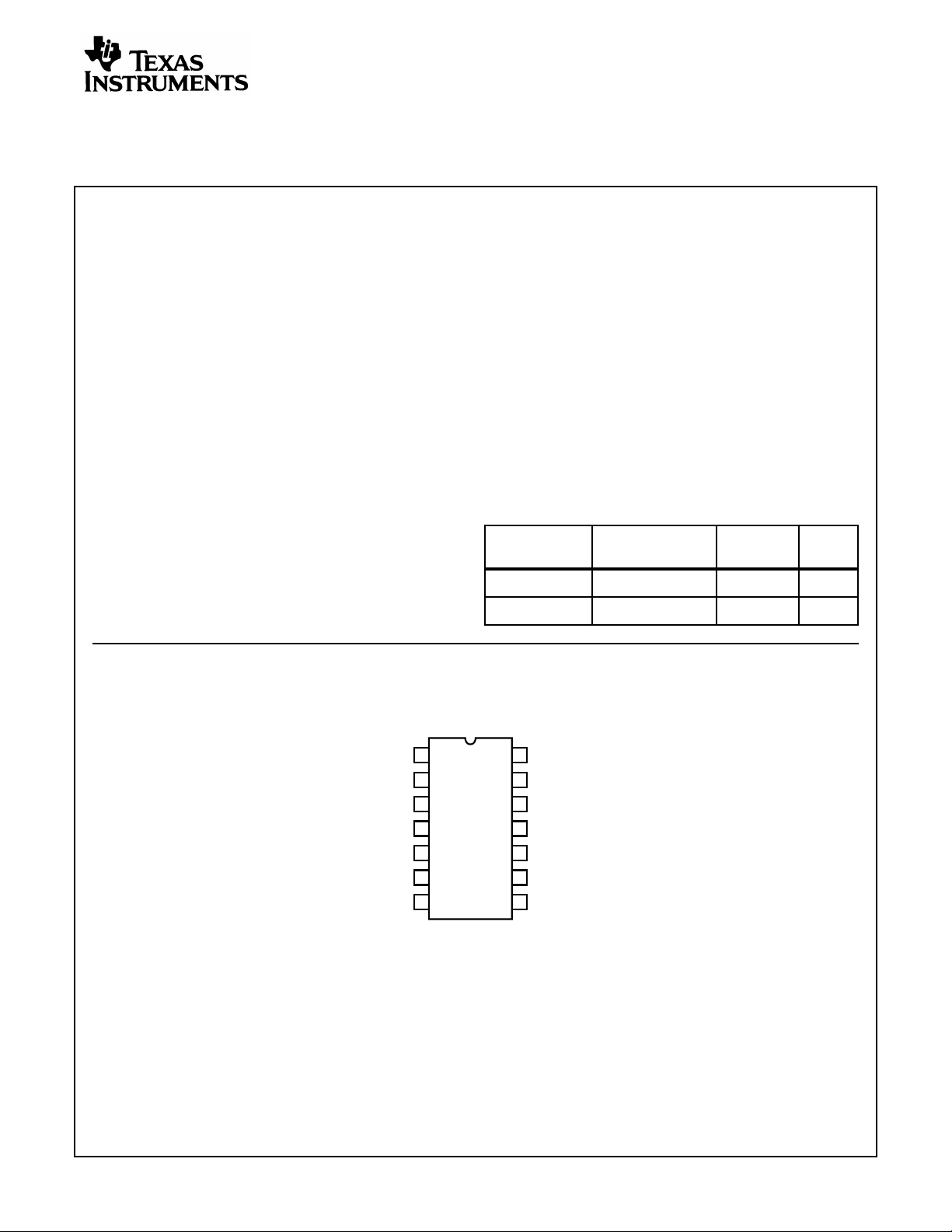
Ordering Information
PART NUMBER TEMP. RANGE (oC) PACKAGE
CD74HC4024E -55 to 125 14 Ld PDIP E14.3
CD74HCT4024M -55 to 125 14 Ld SOIC M14.15
≤ 1µA at VOL, V
l
OH
PKG.
NO.
Pinout
CD74HC4024, CD74HCT4024
(PDIP, SOIC)
TOP VIEW
CP
MR
Q
Q
Q
Q
GND
1
2
3
7
4
6
5
5
6
4
7
V
14
NC
13
12
Q
11
Q
NC
10
9
Q
NC
8
CC
1
2
3
’
CAUTION: These devices are sensitive to electrostatic discharge. Users should follow proper IC Handling Procedures.
Copyright
© Harris Corporation 1997
1
File Number 1683.1
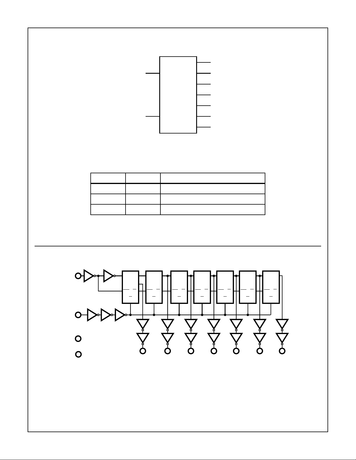
Functional Diagram
CD74HC4024, CD74HCT4024
12
Q1’
1
CP
2
MR
TRUTH TABLE
CP COUNT MR OUTPUT STATE
↑ L No Change
11
Q
2
9
Q
3
6
Q
4
5
Q
5
4
Q
6
3
Q
7
Logic Diagram
1
CP
2
MR
7
GND
14
V
CC
↓ L Advance to Next State
X H All Outputs Are Low
NOTE: H = High Voltage Level, L = Low Voltage Level, X = Don’t Care,
↑ = Transition from Low to High Level, ↓ = Transition from High to Low.
CP
CP
Q
Q1
1
Q
R
Q
CP
2
Q
CP
R
12
’
Q
1
Q
CP
3
Q
CP
R
11
Q
2
Q
CP
4
Q
CP
R
9
Q
3
Q
CP
5
Q
CP
R
6
Q
4
Q
CP
6
Q
CP
R
5
Q
5
Q
CP
7
Q
CP
R
4
Q
6
3
Q
7
2
CD74HC4024, CD74HCT4024
Absolute Maximum Ratings Thermal Information
DC Supply Voltage, VCC. . . . . . . . . . . . . . . . . . . . . . . . -0.5V to 7V
DC Input Diode Current, I
IK
For VI < -0.5V or VI > VCC + 0.5V. . . . . . . . . . . . . . . . . . . . . .±20mA
DC Output Diode Current, I
OK
For VO < -0.5V or VO > VCC + 0.5V . . . . . . . . . . . . . . . . . . . .±20mA
DC Output Source or Sink Current per Output Pin, I
O
For VO > -0.5V or VO < VCC + 0.5V . . . . . . . . . . . . . . . . . . . .±25mA
DC VCC or Ground Current, ICC . . . . . . . . . . . . . . . . . . . . . . . . .±50mA
Operating Conditions
Temperature Range (TA) . . . . . . . . . . . . . . . . . . . . . -55oC to 125oC
Supply Voltage Range, V
HC Types . . . . . . . . . . . . . . . . . . . . . . . . . . . . . . . . . . . . .2V to 6V
HCT Types . . . . . . . . . . . . . . . . . . . . . . . . . . . . . . . . .4.5V to 5.5V
DC Input or Output Voltage, VI, VO . . . . . . . . . . . . . . . . . 0V to V
Input Rise and Fall Time
2V . . . . . . . . . . . . . . . . . . . . . . . . . . . . . . . . . . . . . . 1000ns (Max)
4.5V. . . . . . . . . . . . . . . . . . . . . . . . . . . . . . . . . . . . . . 500ns (Max)
6V . . . . . . . . . . . . . . . . . . . . . . . . . . . . . . . . . . . . . . . 400ns (Max)
CAUTION: Stresses above those listed in “Absolute Maximum Ratings” may cause permanent damage to the device. This is a stress only rating and operation
of the device at these or any other conditions above those indicated in the operational sections of this specification is not implied.
NOTE:
3. θJA is measured with the component mounted on an evaluation PC board in free air.
CC
Thermal Resistance (Typical, Note 3) θJA (oC/W)
PDIP Package. . . . . . . . . . . . . . . . . . . . . . . . . . . . . 90
SOIC Package. . . . . . . . . . . . . . . . . . . . . . . . . . . . . 175
Maximum Junction Temperature. . . . . . . . . . . . . . . . . . . . . . . 150oC
Maximum Storage Temperature Range . . . . . . . . . .-65oC to 150oC
Maximum Lead Temperature (Soldering 10s). . . . . . . . . . . . . 300oC
(SOIC - Lead Tips Only)
CC
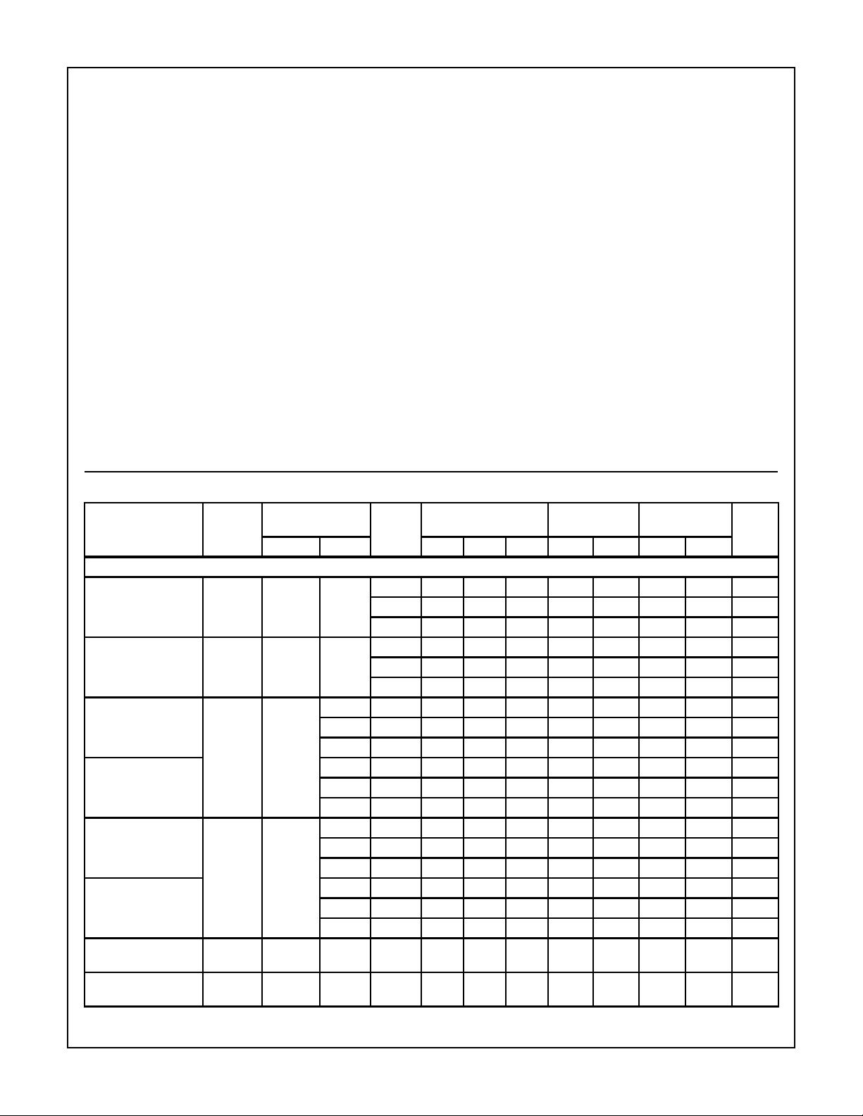
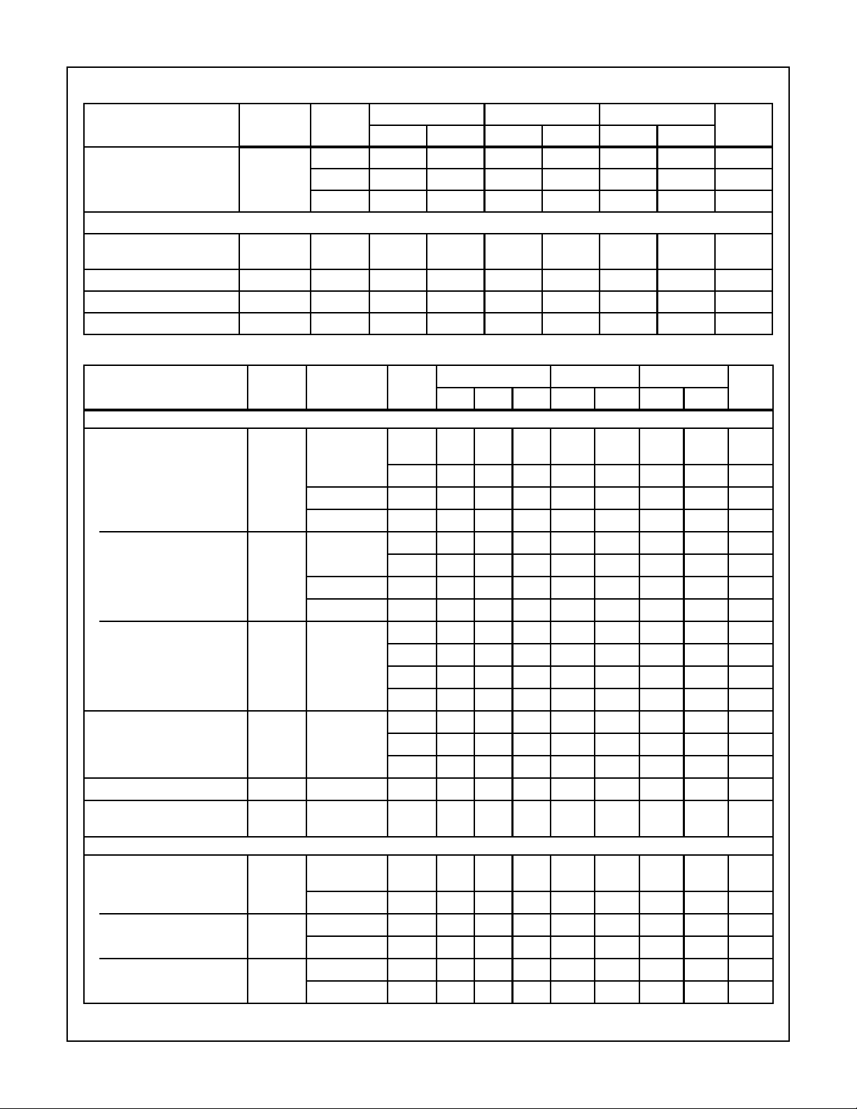
DC Electrical Specifications
PARAMETER SYMBOL
HC TYPES
High Level Input
Voltage
Low Level Input
Voltage
High Level Output
Voltage
CMOS Loads
High Level Output
Voltage
TTL Loads
Low Level Output
Voltage
CMOS Loads
Low Level Output
Voltage
TTL Loads
Input Leakage
Current
Quiescent Device
Current
V
IH
V
IL
V
OH
V
OL
I
I
I
CC
TEST
CONDITIONS
(V) IO(mA) MIN TYP MAX MIN MAX MIN MAX
I
V
CC
(V)
o
C -40oC TO 85oC -55oCTO125oC
25
UNITSV
- - 2 1.5 - - 1.5 - 1.5 - V
4.5 3.15 - - 3.15 - 3.15 - V
6 4.2 - - 4.2 - 4.2 - V
- - 2 - - 0.5 - 0.5 - 0.5 V
4.5 - - 1.35 - 1.35 - 1.35 V
6 - - 1.8 - 1.8 - 1.8 V
VIHor VIL-0.02 2 1.9 - - 1.9 - 1.9 - V
-0.02 4.5 4.4 - - 4.4 - 4.4 - V
-0.02 6 5.9 - - 5.9 - 5.9 - V
- - ---- - - - V
-4 4.5 3.98 - - 3.84 - 3.7 - V
-5.2 6 5.48 - - 5.34 - 5.2 - V
VIHor VIL0.02 2 - - 0.1 - 0.1 - 0.1 V
0.02 4.5 - - 0.1 - 0.1 - 0.1 V
0.02 6 - - 0.1 - 0.1 - 0.1 V
- - ---- - - - V
4 4.5 - - 0.26 - 0.33 - 0.4 V
5.2 6 - - 0.26 - 0.33 - 0.4 V
VCC or
-6--±0.1 - ±1-±1µA
GND
VCC or
0 6 - - 8 - 80 - 160 µA
GND
3
CD74HC4024, CD74HCT4024
DC Electrical Specifications (Continued)
TEST
CONDITIONS
PARAMETER SYMBOL
HCT TYPES
High Level Input
Voltage
Low Level Input
Voltage
High Level Output
Voltage
V
IH
V
IL
V
OH
CMOS Loads
High Level Output
Voltage
TTL Loads
Low Level Output
Voltage
V
OL
CMOS Loads
Low Level Output
Voltage
TTL Loads
Input Leakage
Current
Quiescent Device
Current
Additional Quiescent
Device Current Per
I
I
I
CC
∆I
CC
Input Pin: 1 Unit Load
NOTE: For dual-supply systems theoretical worst case (V
(V) IO(mA) MIN TYP MAX MIN MAX MIN MAX
I
- - 4.5 to
- - 4.5 to
VIHor VIL-0.02 4.5 4.4 - - 4.4 - 4.4 - V
-4 4.5 3.98 - - 3.84 - 3.7 - V
VIHor VIL0.02 4.5 - - 0.1 - 0.1 - 0.1 V
4 4.5 - - 0.26 - 0.33 - 0.4 V
VCCand
0 5.5 - - ±0.1 - ±1-±1µA
GND
VCC or
0 5.5 - - 8 - 80 - 160 µA
GND
V
CC
- 4.5 to
-2.1
o
C -40oC TO 85oC -55oCTO125oC
V
CC
25
(V)
2--2- 2 - V
5.5
- - 0.8 - 0.8 - 0.8 V
5.5
- 100 360 - 450 - 490 µA
5.5
= 2.4V, VCC = 5.5V) specification is 1.8mA.
I
UNITSV
HCT Input Loading Table
INPUT UNIT LOADS
CP, MR 0.5
NOTE: Unit Load is ∆ICClimit specified in DC Electrical Table, e.g.,
360µA max at 25oC.
Prerequisite for Switching Specifications
PARAMETER SYMBOL VCC (V)
HC TYPES
Maximum Input Pulse
Frequency
Input Pulse Width t
Reset Removal Time t
f
MAX
W
REM
26-5-4-MHz
4.5 30 - 24 - 20 - MHz
635-29-24-MHz
2 80 - 100 - 120 - ns
4.516-20-24-ns
614-17-20-ns
250-65-75-ns
4.510-13-15-ns
6 9 -11-13-ns
o
25
C -40oC TO 85oC -55oC TO 125oC
UNITSMIN MAX MIN MAX MIN MAX
4
CD74HC4024, CD74HCT4024
Prerequisite for Switching Specifications (Continued)
25
PARAMETER SYMBOL V
Reset Pulse Width t
HCT TYPES
Maximum Input Pulse
Frequency
Input Pulse Width t
Reset Recovery Time t
Reset Pulse Width t
f
MAX
REC
W
W
W
(V)
CC
2 80 - 100 - 120 - ns
4.516-20-24-ns
614-17-20-ns
4.5 25 - 20 - 16 - MHz
4.520-25-30-ns
4.510-13-15-ns
4.520-25-30-ns
o
C -40oC TO 85oC -55oC TO 125oC
UNITSMIN MAX MIN MAX MIN MAX
Switching Specifications Input t
PARAMETER SYMBOL
, tf = 6ns
r
CONDITIONS
TEST
V
CC
25oC -40oC TO 85oC -55oCTO125oC
(V)
HC TYPES
Propagation Delay Time
(Figure 1)
t
PLH,
t
PHL
CL= 50pF 2 - - 140 - 175 - 210 ns
CP to Q1’ Output 4.5 - - 28 - 35 - 42 ns
CL=15pF 5 - 11 - - - - - ns
CL= 50pF 6 - - 24 - 30 - 36 ns
Qnto Qn+ 1 t
PLH,
t
CL= 50pF 2 - - 75 - 95 - 110 ns
PHL
4.5 - - 15 - 19 - 22 ns
CL=15pF 5 - 6 - - - - - ns
CL= 50pF 6 - - 13 - 13 - 19 ns
MR to Q
n
t
PLH,
t
PHL
CL= 50pF 2 - - 170 - 215 - 255 ns
4.5 - - 34 - 43 - 51 ns
5 - 14 - - - - - ns
6 - - 29 - 27 - 43 ns
Output Transition Time
(Figure 1)
t
TLH,tTHLCL
= 50pF 2 - - 75 - 95 - 110 ns
4.5 - - 15 - 19 - 22 ns
6 - - 13 - 16 - 19 ns
Input Capacitance C
Power Dissipation Capacitance
C
CL= 50pF - - - 10 - 10 - 10 pF
IN
CL=15pF 5 - 30 - - - - - pF
PD
(Notes 4, 5)
HCT TYPES
Propagation Delay Time
(Figure 2)
t
PLH,
t
PHL
CL= 50pF 4.5 - - 40 - 50 - 60 ns
CP to Q1’ Output CL=15pF 5 - 17 - - - - - ns
Qnto Qn+ 1 t
MR to Q
n
PLH,
t
t
PLH,
t
CL= 50pF 4.5 - - 15 - 19 - 22 ns
PHL
CL=15pF 5 - 6 - - - - - ns
CL= 50pF 4.5 - - 40 - 50 - 60 ns
PHL
CL=15pF 5 - 17 - - - - - ns
UNITSMIN TYP MAX MIN MAX MIN MAX
5

CD74HC4024, CD74HCT4024
Switching Specifications Input t
PARAMETER SYMBOL
Output Transition t
Input Capacitance C
Power Dissipation Capacitance
, tf = 6ns (Continued)
r
CONDITIONS
TLH,tTHLCL
CL=15pF - - - 10 - 10 - 10 pF
IN
C
CL=15pF 5 - 30 - - - - - pF
PD
TEST
V
CC
(V)
= 50pF 4.5 - - 15 - 19 - 22 ns
(Notes 4, 5)
NOTES:
4. CPD is used to determine the dynamic power consumption, per package.
5. PD=V
CC
2
fi+ ∑ (CLV
2
fi/M) where: M = 21,22,23,24,25,26,27fi= Input Frequency, CL= Output Load Capacitance, VCC= Supply
CC
Voltage.
Test Circuits and Waveforms
trC
L
CLOCK
10%
90%
50%
10%
tfC
t
L
WL
tWL+ tWH=
50%
t
WH
NOTE: Outputs should be switching from 10% VCC to 90% VCC in
accordance with device truth table.For f
, input duty cycle = 50%.
MAX
FIGURE 1. HC CLOCK PULSE RISE AND FALLTIMES AND
PULSE WIDTH
fC
50%
I
L
V
CC
GND
NOTE: Outputs should be switching from 10% VCC to 90% VCC in
accordance with device truth table.For f
25oC -40oC TO 85oC -55oCTO125oC
UNITSMIN TYP MAX MIN MAX MIN MAX
t
rCL
CLOCK
= 6ns
0.3V
2.7V
1.3V
0.3V
t
t
fCL
WL
= 6ns
+ tWH=
t
WL
1.3V
t
WH
, input duty cycle = 50%.
MAX
I
fC
3V
1.3V
GND
FIGURE 2. HCT CLOCK PULSE RISE AND FALLTIMES AND
PULSE WIDTH
L
tr = 6ns tf = 6ns
V
t
CC
GND
TLH
INPUT
t
INVERTING
OUTPUT
THL
t
PHL
90%
50%
10%
t
PLH
90%
50%
10%
FIGURE 3. HC AND HCU TRANSITION TIMES AND PROPAGA-
TION DELAY TIMES, COMBINATION LOGIC
= 6ns
t
PLH
t
f
1.3V
10%
90%
t
3V
GND
TLH
tr = 6ns
INPUT
INVERTING
OUTPUT
t
THL
t
2.7V
1.3V
0.3V
PHL
FIGURE 4. HCT TRANSITION TIMES AND PROPAGATION
DELAY TIMES, COMBINATION LOGIC
6

IMPORTANT NOTICE
T exas Instruments and its subsidiaries (TI) reserve the right to make changes to their products or to discontinue
any product or service without notice, and advise customers to obtain the latest version of relevant information
to verify, before placing orders, that information being relied on is current and complete. All products are sold
subject to the terms and conditions of sale supplied at the time of order acknowledgement, including those
pertaining to warranty, patent infringement, and limitation of liability.
TI warrants performance of its semiconductor products to the specifications applicable at the time of sale in
accordance with TI’s standard warranty. Testing and other quality control techniques are utilized to the extent
TI deems necessary to support this warranty . Specific testing of all parameters of each device is not necessarily
performed, except those mandated by government requirements.
CERT AIN APPLICATIONS USING SEMICONDUCTOR PRODUCTS MAY INVOLVE POTENTIAL RISKS OF
DEATH, PERSONAL INJURY, OR SEVERE PROPERTY OR ENVIRONMENTAL DAMAGE (“CRITICAL
APPLICATIONS”). TI SEMICONDUCTOR PRODUCTS ARE NOT DESIGNED, AUTHORIZED, OR
WARRANTED TO BE SUITABLE FOR USE IN LIFE-SUPPORT DEVICES OR SYSTEMS OR OTHER
CRITICAL APPLICA TIONS. INCLUSION OF TI PRODUCTS IN SUCH APPLICATIONS IS UNDERST OOD TO
BE FULLY AT THE CUSTOMER’S RISK.
In order to minimize risks associated with the customer’s applications, adequate design and operating
safeguards must be provided by the customer to minimize inherent or procedural hazards.
TI assumes no liability for applications assistance or customer product design. TI does not warrant or represent
that any license, either express or implied, is granted under any patent right, copyright, mask work right, or other
intellectual property right of TI covering or relating to any combination, machine, or process in which such
semiconductor products or services might be or are used. TI’s publication of information regarding any third
party’s products or services does not constitute TI’s approval, warranty or endorsement thereof.
Copyright 1999, Texas Instruments Incorporated
 Loading...