

Texas Instruments CD74HCT40105M96, CD74HCT40105M, CD74HCT40105E, CD74HC40105M, CD74HC40105E Datasheet
...
CD74HC40105,
[ /Title
(CD74
HC401
05,
CD74
HCT40
105)
/Subject
(High
Speed
CMOS
Data sheet acquired from Harris Semiconductor
SCHS222
February 1998
Features
• Independent Asynchronous Inputs and Outputs
• Expandable in Either Direction
• Reset Capability
• Status Indicators on Inputs and Outputs
• Three-State Outputs
• Shift-Out Independent of Three-State Control
• Fanout (Over Temperature Range)
- Standard Outputs. . . . . . . . . . . . . . . 10 LSTTL Loads
- Bus Driver Outputs . . . . . . . . . . . . . 15 LSTTL Loads
• Wide Operating Temperature Range . . . -55
• Balanced Propagation Delay and Transition Times
• Significant Power Reduction Compared to LSTTL
Logic ICs
• HC Types
- 2V to 6V Operation
- High Noise Immunity: N
at VCC = 5V
• HCT Types
- 4.5V to 5.5V Operation
- Direct LSTTL Input Logic Compatibility,
V
= 0.8V (Max), VIH = 2V (Min)
IL
- CMOS Input Compatibility, I
= 30%, NIH = 30% of V
IL
≤ 1µA at VOL, V
l
o
Applications
• Bit-Rate Smoothing
• CPU/Terminal Buffering
• Data Communications
• Peripheral Buffering
• Line Printer Input Buffers
• Auto-Dialers
• CRT Buffer Memories
• Radar Data Acquisition
C to 125oC
CC
OH
CD74HCT40105
High Speed CMOS Logic
4-Bit x 16-Word FIFO Register
Description
The Harris CD74HC40105 and CD74HCT40105 are highspeed silicon-gate CMOS devices that are compatible,
except for “shift-out” circuitry, with the Harris CD40105B.
They are low-power first-in-out (FIFO) “elastic” storage
registers that can store 16 four-bit words. The 40105 is
capable ofhandling input and outputdata at different shifting
rates. This feature makes particularly useful as a buffer
between asynchronous systems.
Each work position in the register is clocked by a control flipflop, which stores a marker bit. A “1” signifies that the position’s data is filled and a “0” denotes a vacancy in that position. The control flip-flop detects the state of the preceding
flip-flop and communicates its own status to the succeeding
flip-flop. When a control flip-flop is in the “0” state and sees a
“1” in the preceeding flip-flop, it generates a clock pulse that
transfers data from the preceding four data latches into its
own four data latches and resets the preceding flip-flop to
“0”. The first and last control flip-flops have buffered outputs.
Since all empty locations “bubble” automatically to the input
end, and all valid data ripple through to the output end, the
status of the first control flip-flop (DATA-IN READY) indicates
if the FIFO is full, and the status of the last flip-flop (DATAOUT READY) indicates if the FIFO contains data. As the
earliest data are removed from the bottom of the data stack
(the output end), all data entered later will automatically
propagate (ripple) toward the output.
Ordering Information
TEMP. RANGE
PART NUMBER
CD74HC40105E -55 to 125 16 Ld PDIP E16.3
CD74HCT40105E -55 to 125 16 Ld PDIP E16.3
CD74HC40105M -55 to 125 16 Ld SOIC M16.15
CD74HCT40105M -55 to 125 16 Ld SOIC M16.15
NOTES:
1. When ordering,use the entire partnumber. Add the suffix 96 to
obtain the variant in the tape and reel.
2. Wafer and die for this part number is available which meets all
electrical specifications. Please contact your local sales office or
Harris customer service for ordering information.
(oC) PACKAGE PKG. NO.
CAUTION: These devices are sensitive to electrostatic discharge. Users should follow proper IC Handling Procedures.
Copyright
© Harris Corporation 1998
1
File Number 1834.1
CD74HC40105, CD74HCT40105
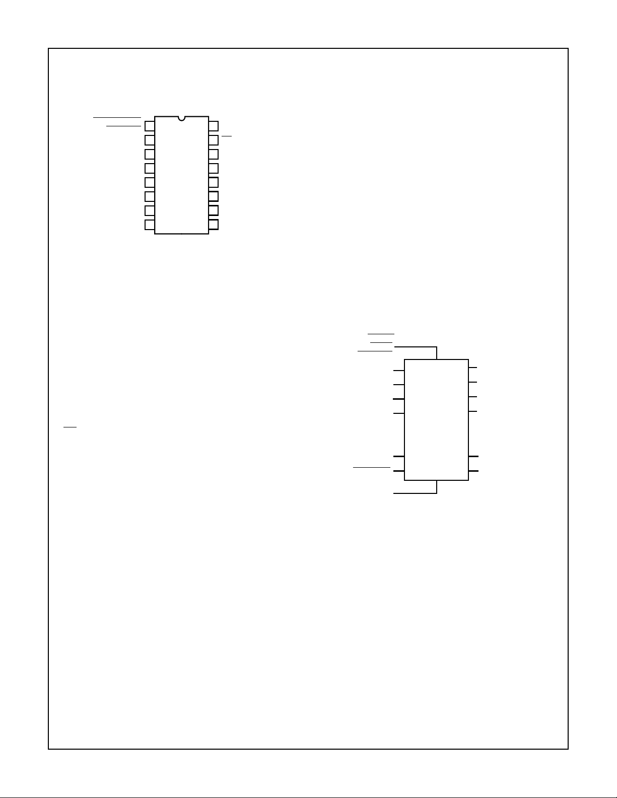
Pinout
CD74HC40105, CD74HCT40105
(PDIP, SOIC)
TOP VIEW
THREE-STATE
CONTROL
DIR
D0
D1
D2
D3
GND
1
2
3
SI
4
5
6
7
8
Loading Data
Data can be entered whenever the DATA-IN READY (DIR)
flag is high, by a low to high transition on the SHIFT-IN (SI)
input. This input must go low momentarily before the next
word is accepted by the FIFO. The DIR flag will go low
momentarily, until the data have been transferred to the second location. The flag will remain low when all 16-word locations are filled with valid data, and further pulses on the SI
input will be ignored until DIR goes high.
Unloading Data
As soon as the first word has rippled to the output, the dataout ready output (DOR) goes HIGH and data of the first word
is available on the outputs. Data of other words can be
removed by a negative-going transition on the shift-out input
(
SO). This negative-going transition causes the DOR signal
to go LOW while the next word moves to the output. As long
as valid data is available in the FIFO, the DOR signal will go
high again, signifying that the next word is ready at the
output. When the FIFO is empty, DOR will remain LOW, and
any further commands will be ignored until a “1” marker
ripples down to the last control register and DOR goes
HIGH. If during unloading SI is HIGH, (FIFO is full) data on
the data input of the FIFO is entered in the first location.
V
16
CC
15
SO
14
DOR
13
Q0
12
Q1
Q2
11
10
Q3
MR
9
Three-State Outputs
In order to facilitate data busing, three-state outputs (Q0 to
Q3) are provided on the data output lines, while the load
condition of the register can be detected by the state of the
DOR output. A HIGH on the three-state control flag (output
enable input OE) forces the outputs into the high-impedance
OFF-state mode. Note that the shift-out signal, unlike that in
the Harris CD40105B, is independent of the three-state
output control. In the CD40105B, the three-state control
must not be shifted from High to Low when the shift-out
signal is Low (data loss would occur). In the high-speed
CMOS version this restriction has been eliminated.
Cascading
The 40105 can be cascaded to form longer registers simply
by connecting the DIR to SO and DOR to SI. In the cascaded
mode, a MASTER RESET pulse must be applied after the
supply voltage is turnedon. For words wider than four bits, the
DIR and the DOR outputs must be gated together with AND
gates. Theri outputs drive the SI and SO inputs in parallel, if
expanding is done in both directions (see Figures 12 and 13).
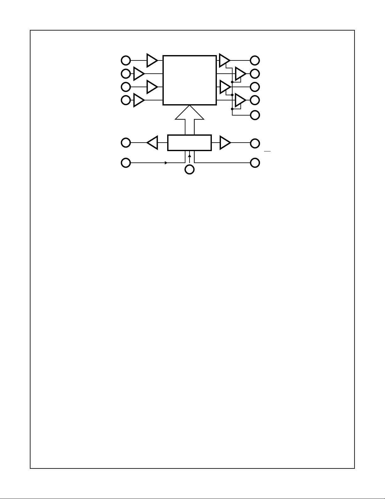
Functional Diagram
THREE-
STATE
CONTROL
D0
D1
D2
D3
SHIFT IN
SHIFT OUT
MASTER
RESET
4
5
6
7
3
15
1
9
GND = 8
V
= 16
CC
13
Q0
12
Q1
11
Q2
10
Q3
14
DATA-OUT
READY
2
DATA-IN
READY
Master Reset
A high on the MASTER RESET (MR) sets all the control
logic marker bits to “0”. DOR goes low and DIR goes high.
The contents of the data register are not changed, only
declared invalid, and will be superseded when the first word
is loaded. Thus, MR does not clear data within the register
but only the control logic. If the shift-in flag (SI) is HIGH
during the master reset pulse, data present at the input (D0
to D3) are immediately moved into the first location upon
completion of the reset process.
2
CD74HC40105, CD74HCT40105
INPUT
BUFFERS
4
D0
5
D1
6
D2
7
D3
DATA-IN READY (DIR)
2 CONTROL LOGIC
3 15
SHIFT IN (SI)
FIGURE 1. FUNCTIONAL BLOCK DIAGRAM
4 x 16
DAT A
REGISTER
9
MASTER
RESET
(MR)
OUTPUT
BUFFERS
13
Q0
12
Q1
11
Q2
10
Q3
1
THREE-STATE CONTROL
DATA-OUT READY (DOR)
14
SHIFT OUT (
SO)
3
MR
DIR
D0
D1
D2
D3
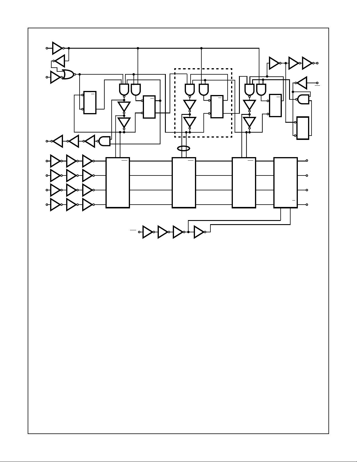
CD74HC40105, CD74HCT40105
9
14
3
SI
F/Fs
R Q
†
QS
2
4
CL CL
5
4
6
7
LATCHES
L1
POSITION 1
F/F1
R Q
† †
QS
14 x
CL CL
4 x 14
LATCHES
14 x L1
POSITION 2-15 POSITIONS 16
2-15
R Q
† †
QS
14 x
CL CL
4
LATCHES
L16
F/F16
R Q
† †
QS
THREE-
OUTPUT
BUFFERS
E
STATE
DOR
15
S0
R
†
QS
13
Q0
12
Q1
11
Q2
10
E
Q3
† “S” overrides “R”.
†† “R” overrides “S”.
1
OE
FIGURE 2. LOGIC DIAGRAM
4
CD74HC40105, CD74HCT40105
Absolute Maximum Ratings Thermal Information
DC Supply Voltage, VCC. . . . . . . . . . . . . . . . . . . . . . . . -0.5V to 7V
DC Input Diode Current, I
IK
For VI < -0.5V or VI > VCC + 0.5V. . . . . . . . . . . . . . . . . . . . . .±20mA
DC Output Diode Current, I
OK
For VO < -0.5V or VO > VCC + 0.5V . . . . . . . . . . . . . . . . . . . .±20mA
DC Output Source or Sink Current per Output Pin, I
O
For VO > -0.5V or VO < VCC + 0.5V . . . . . . . . . . . . . . . . . . . .±25mA
DC VCC or Ground Current, ICC . . . . . . . . . . . . . . . . . . . . . . . . .±50mA
Operating Conditions
Temperature Range (TA) . . . . . . . . . . . . . . . . . . . . . -55oC to 125oC
Supply Voltage Range, V
HC Types . . . . . . . . . . . . . . . . . . . . . . . . . . . . . . . . . . . . .2V to 6V
HCT Types . . . . . . . . . . . . . . . . . . . . . . . . . . . . . . . . .4.5V to 5.5V
DC Input or Output Voltage, VI, VO . . . . . . . . . . . . . . . . . 0V to V
Input Rise and Fall Time
2V . . . . . . . . . . . . . . . . . . . . . . . . . . . . . . . . . . . . . . 1000ns (Max)
4.5V. . . . . . . . . . . . . . . . . . . . . . . . . . . . . . . . . . . . . . 500ns (Max)
6V . . . . . . . . . . . . . . . . . . . . . . . . . . . . . . . . . . . . . . . 400ns (Max)
CAUTION: Stresses above those listed in “Absolute Maximum Ratings” may cause permanent damage to the device. This is a stress only rating and operation
of the device at these or any other conditions above those indicated in the operational sections of this specification is not implied.
NOTE:
3. θJA is measured with the component mounted on an evaluation PC board in free air.
CC
Thermal Resistance (Typical, Note 3) θJA (oC/W)
PDIP Package. . . . . . . . . . . . . . . . . . . . . . . . . . . . . 90
SOIC Package. . . . . . . . . . . . . . . . . . . . . . . . . . . . . 160
Maximum Junction Temperature . . . . . . . . . . . . . . . . . . . . . . . 150oC
Maximum Storage Temperature Range . . . . . . . . . .-65oC to 150oC
Maximum Lead Temperature (Soldering 10s) . . . . . . . . . . . . . 300oC
(SOIC - Lead Tips Only)
CC
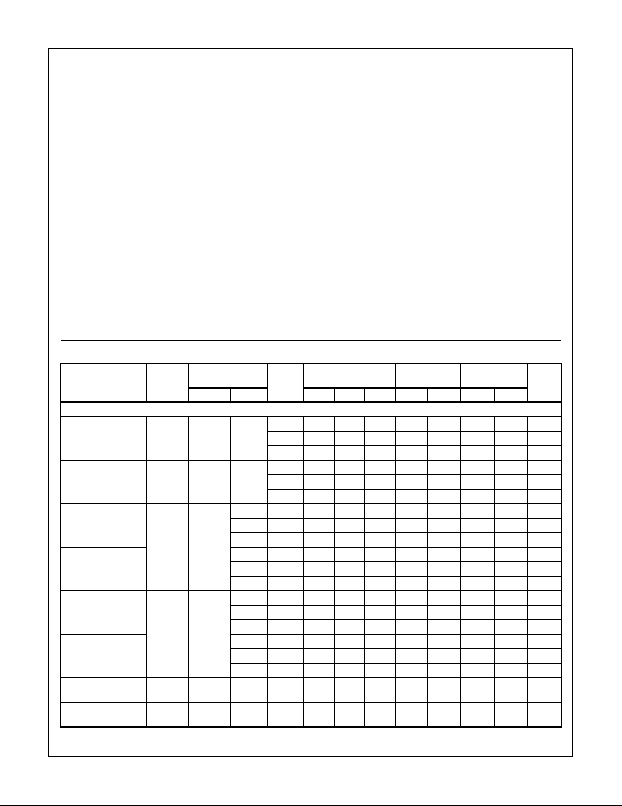
DC Electrical Specifications
PARAMETER SYMBOL
HC TYPES
High Level Input
Voltage
Low Level Input
Voltage
High Level Output
Voltage
CMOS Loads
High Level Output
Voltage
TTL Loads
Low Level Output
Voltage
CMOS Loads
Low Level Output
Voltage
TTL Loads
Input Leakage
Current
Quiescent Device
Current
V
IH
V
IL
V
OH
V
OL
I
I
I
CC
TEST
CONDITIONS
(V) IO(mA) MIN TYP MAX MIN MAX MIN MAX
I
V
CC
(V)
o
C -40oC TO 85oC -55oCTO125oC
25
UNITSV
- - 2 1.5 - - 1.5 - 1.5 - V
4.5 3.15 - - 3.15 - 3.15 - V
6 4.2 - - 4.2 - 4.2 - V
- - 2 - - 0.5 - 0.5 - 0.5 V
4.5 - - 1.35 - 1.35 - 1.35 V
6 - - 1.8 - 1.8 - 1.8 V
VIHor VIL-0.02 2 1.9 - - 1.9 - 1.9 - V
-0.02 4.5 4.4 - - 4.4 - 4.4 - V
-0.02 6 5.9 - - 5.9 - 5.9 - V
- - ---- - - - V
-4 4.5 3.98 - - 3.84 - 3.7 - V
-5.2 6 5.48 - - 5.34 - 5.2 - V
VIHor VIL0.02 2 - - 0.1 - 0.1 - 0.1 V
0.02 4.5 - - 0.1 - 0.1 - 0.1 V
0.02 6 - - 0.1 - 0.1 - 0.1 V
- - ---- - - - V
4 4.5 - - 0.26 - 0.33 - 0.4 V
5.2 6 - - 0.26 - 0.33 - 0.4 V
VCC or
-6--±0.1 - ±1-±1µA
GND
VCC or
0 6 - - 8 - 80 - 160 µA
GND
5

CD74HC40105, CD74HCT40105
DC Electrical Specifications (Continued)
TEST
CONDITIONS
PARAMETER SYMBOL
Three-State Leakage
I
OZ
Current
HCT TYPES
High Level Input
Voltage
Low Level Input
Voltage
High Level Output
Voltage
V
IH
V
IL
V
OH
CMOS Loads
High Level Output
Voltage
TTL Loads
Low Level Output
Voltage
V
OL
CMOS Loads
Low Level Output
Voltage
TTL Loads
Input Leakage
Current
Quiescent Device
Current
Three-State Leakage
Current
Additional Quiescent
Device Current Per
I
I
I
CC
I
OZ
∆I
CC
(Note)
Input Pin: 1 Unit Load
NOTE: For dual-supply systems theoretical worst case (V
(V) IO(mA) MIN TYP MAX MIN MAX MIN MAX
I
VILor VIHVO =
VCC or
GND
- - 4.5 to
- - 4.5 to
VIHor VIL-0.02 4.5 4.4 - - 4.4 - 4.4 - V
-4 4.5 3.98 - - 3.84 - 3.7 - V
VIHor VIL0.02 4.5 - - 0.1 - 0.1 - 0.1 V
4 4.5 - - 0.26 - 0.33 - 0.4 V
VCCand
0 5.5 - - ±0.1 - ±1-±1µA
GND
VCC or
0 5.5 - - 8 - 80 - 160 µA
GND
VILor VIHVO =
VCC or
GND
V
CC
- 4.5 to
-2.1
o
C -40oC TO 85oC -55oCTO125oC
V
CC
25
(V)
6--±0.5 - ±5-±10 µA
2--2- 2 - V
5.5
- - 0.8 - 0.8 - 0.8 V
5.5
5.5 - - ±0.5 - ±5-±10 µA
- 100 360 - 450 - 490 µA
5.5
= 2.4V, VCC = 5.5V) specification is 1.8mA.
I
UNITSV
HCT Input Loading Table
INPUT UNIT LOADS
OE 0.75
SI, SO 0.4
Dn 0.3
MR 1.5
NOTE: Unit Load is ∆ICClimit specified in DC Electrical Table, e.g.,
360µA max at 25oC.
6

CD74HC40105, CD74HCT40105
Prerequisite for Switching Specifications
PARAMETER SYMBOL VCC (V)
HC TYPES
SI Pulse Width
HIGH or LOW
SO Pulse Width
HIGH or LOW
DIR Pulse Width
HIGH or LOW
DOR Pulse Width
HIGH or LOW
MR Pulse Width HIGH t
Removal Time
MR to SI
Set-Up Time
Dn to SI
Hold Time
Dn to SI
Maximum Pulse Frequency
SI, SO
HCT TYPES
SI Pulse Width HIGH or LOW t
SO Pulse Width HIGH or
LOW
DIR Pulse Width HIGH or
LOW
DOR Pulse Width HIGH or
LOW
MR Pulse Width HIGH t
Removal Time MR to SI t
Set-Up Time Dn to SI t
Hold Time Dn to SI t
Maximum Pulse Frequency
SI, SO
t
t
t
t
t
REM
t
SU
t
f
MAX
t
t
t
REM
SU
f
MAX
W
2 80 - 100 - 120 - ns
4.5 16 - 20 - 24 - ns
6 14 - 17 - 20 - ns
W
2 120 - 150 - 180 - ns
4.5 24 - 30 - 36 - ns
6 20 - 26 - 31 - ns
W
2 200 - 250 - 300 - ns
4.5 40 - 50 - 60 - ns
6 34 - 43 - 51 - ns
W
2 200 - 250 - 300 - ns
4.5 40 - 50 - 60 - ns
6 34 - 43 - 51 - ns
W
2 120 - 150 - 180 - ns
4.5 24 - 30 - 36 - ns
6 20 - 26 - 31 - ns
2 50 - 65 - 75 - ns
4.5 10 - 13 - 15 - ns
6 9 -11-13-ns
2 5-5-5-ns
4.5 5 - 5 - 5 - ns
6 5-5-5-ns
H
2 125 - 155 - 190 - ns
4.5 25 - 31 - 38 - ns
6 21 - 26 - 32 - ns
2 3-2-2-MHz
4.5 15 - 12 - 10 - MHz
6 18 - 14 - 12 - MHz
W
W
W
W
W
4.5 16 - 20 - 24 - ns
4.5 16 - 20 - 24 - ns
4.5 40 - 50 - 60 - ns
4.5 40 - 50 - 60 - ns
4.5 24 - 30 - 36 - ns
4.5 15 - 19 - 22 - ns
4.5 0 - 0 - 0 - ns
H
4.5 25 - 31 - 38 - ns
4.5 15 - 12 - 10 - MHz
25oC -40oC TO 85oC -55oC TO 125oC
UNITSMIN MAX MIN MAX MIN MAX
7

CD74HC40105, CD74HCT40105
Switching Specifications Input t
PARAMETER SYMBOL
, tf = 6ns
r
CONDITIONS
TEST
V
CC
25oC -40oC TO 85oC -55oCTO125oC
(V)
HC TYPES
Propagation Delay t
MR to DIR, DOR CL= 50pF 4.5 - - 35 - 44 - 53 ns
PHL,
t
CL= 50pF 2 - - 175 - 220 - 265 ns
PLH
CL= 15pF 5 - 15 - - - - - ns
CL= 50pF 6 - - 30 - 37 - 45 ns
SI to DIR t
PHL,
t
CL= 50pF 2 - - 210 - 265 - 315 ns
PLH
CL= 50pF 4.5 - - 42 - 53 - 63 ns
CL= 15pF 5 - 18 - - - - - ns
CL= 50pF 6 - - 36 - 45 - 54 ns
SO to DOR t
PHL,
t
CL= 50pF 2 - - 210 - 265 - 315 ns
PLH
CL= 50pF 4.5 - - 42 - 53 - 63 ns
CL= 15pF 5 - 18 - - - - - ns
CL= 50pF 6 - - 36 - 45 - 54 ns
SO to Qn t
PHL,
t
CL= 50pF 2 - - 400 - 500 - 600 ns
PLH
CL= 50pF 4.5 - - 80 - 100 - 120 ns
CL= 15pF 5 - 35 - - - - - ns
CL= 50pF 6 - - 68 - 85 - 102 ns
Propagation Delay/Ripple thru
Delay
SI to DOR
t
PLH
CL= 50pF 2 - - 2000 - 2500 - 3000 ns
4.5 - - 400 - 500 - 600 ns
6 - - 340 - 425 - 510 ns
Propagation Delay/Ripple thru
Delay
SO to DIR
t
PLH
CL= 50pF 2 - - 2500 - 3125 - 3750 ns
4.5 - - 500 - 625 - 750 ns
6 - - 425 - 532 - 638 ns
Propagation Delay/Ripple thru
Delay
SI to Qn
t
PLH
CL= 50pF 2 - - 1500 - 1900 - 2250 ns
4.5 - - 300 - 380 - 450 ns
6 - - 260 - 330 - 380 ns
Three-State Output Enable
OE to Q
n
t
PZH,tPZLCL
= 50pF 2 - - 150 - 190 - 225 ns
4.5 - - 30 - 38 - 45 ns
6 - - 26 - 33 - 38 ns
Three-State Output Disabe
OE to Qn
t
PHZ,tPLZCL
= 50pF 2 - - 140 - 175 - 210 ns
CL= 50pF 4.5 - - 28 - 35 - 42 ns
CL= 50pF 6 - - 24 - 30 - 36 ns
Output Transition Time t
TLH,tTHLCL
= 50pF 2 - - 75 - 95 - 110 ns
4.5 - - 15 - 19 - 22 ns
6 - - 13 - 16 - 19 ns
Maximum SI, SO Frequency f
Input Capacitance C
Power Dissipation Capacitance
MAX
C
CL= 15pF 5 - 32 - - - - - MHz
CL= 50pF - - - 10 - 10 - 10 pF
IN
CL= 15pF 5 - 83 - - - - - pF
PD
(Notes 4, 5)
UNITSMIN TYP MAX MIN MAX MIN MAX
8

CD74HC40105, CD74HCT40105
Switching Specifications Input t
PARAMETER SYMBOL
Three-State Output
, tf = 6ns (Continued)
r
TEST
CONDITIONS
C
CL= 50pF - - - 15 - 15 - 15 pF
O
V
CC
(V)
25oC -40oC TO 85oC -55oCTO125oC
Capacitance
HCT TYPES
Propagation Delay Time t
MR to DIR, DOR CL= 15pF 5 - 15 - - - - - ns
SI to DIR t
PLH,
t
PLH,
t
SO to DOR t
PLH,
t
SO to Qn t
PLH,
t
Propagation Delay/Ripple thru
t
CL= 50pF 4.5 - - 36 - 45 - 54 ns
PHL
CL= 50pF 4.5 - - 42 - 53 - 63 ns
PHL
CL=15pF 5 - 18 - - - - - ns
CL= 50pF 4.5 - - 42 - 53 - 63 ns
PHL
CL=15pF 5 - 18 - - - - - ns
CL= 50pF 4.5 - - 80 - 100 - 120 ns
PHL
CL=15pF 5 - 35 - - - - - ns
CL= 50pF 4.5 - - 400 - 500 - 600 ns
PLH
Delay
SI to DOR
Propagation Delay/Ripple thru
t
PLH
CL= 50pF 4.5 - - 500 - 625 - 750 ns
Delay
SO to DIR
Propagation Delay/Ripple thru
t
PLH
CL= 50pF 4.5 - - 300 - 380 - 450 ns
Delay
SI to Qn
Three-State Output Enable
OE to Q
n
Three-State Output Disabe
t
PZH,tPZLCL
t
PHZ,tPLZCL
= 50pF 4.5 - - 35 - 44 - 53 ns
= 50pF 4.5 - - 30 - 38 - 45 ns
OE to Qn
Output Transition Time t
TLH,tTHLCL
Maximum CP Frequency f
Input Capacitance C
Power Dissipation Capacitance
MAX
C
PD
IN
= 50pF 4.5 - - 15 - 19 - 22 ns
CL=15pF 5 - 32 - - - - - MHz
CL= 50pF - - - 10 - 10 - 10 pF
CL=15pF 5 - 83 - - - - - pF
(Notes 4, 5)
Three-State Output
C
CL= 50pF - - - 15 - 15 - 15 pF
O
Capacitance
NOTES:
4. CPD is used to determine the dynamic power consumption, per package.
5. PD=CPDV
CC
2
fi+ Σ (CLV
2
fo) where fi= Input Frequency, fo= Output Frequency, CL= Output Load Capacitance, VCC= Supply
CC
Voltage.
UNITSMIN TYP MAX MIN MAX MIN MAX
9

Test Circuits and Waveforms
trC
L
CLOCK
10%
90%
50%
10%
tfC
t
L
WL
tWL+ tWH=
50%
t
CD74HC40105, CD74HCT40105
WH
fC
50%
I
L
V
CC
GND
t
rCL
CLOCK
= 6ns
2.7V
0.3V
1.3V
0.3V
t
t
fCL
WL
= 6ns
1.3V
t
WH
t
WL
+ tWH=
1.3V
I
fC
L
3V
GND
NOTE: Outputs should be switching from 10% VCC to 90% VCC in
accordance with device truth table. For f
, input duty cycle = 50%.
MAX
FIGURE 3. HC CLOCK PULSE RISE AND FALL TIMES AND
PULSE WIDTH
tr = 6ns tf = 6ns
V
t
CC
GND
TLH
INPUT
t
INVERTING
OUTPUT
THL
t
PHL
90%
50%
10%
t
PLH
90%
50%
10%
FIGURE 5. HC TRANSITION TIMES AND PROPAGATION
DELAY TIMES, COMBINATION LOGIC
NOTE: Outputs should be switching from 10% VCC to 90% VCC in
accordance with device truth table. For f
, input duty cycle = 50%.
MAX
FIGURE 4. HCT CLOCK PULSE RISE AND FALL TIMES AND
PULSE WIDTH
= 6ns
t
PLH
t
f
1.3V
10%
90%
t
3V
GND
TLH
tr = 6ns
INPUT
t
INVERTING
OUTPUT
THL
t
PHL
2.7V
1.3V
0.3V
FIGURE 6. HCT TRANSITION TIMES AND PROPAGATION
DELAY TIMES, COMBINATION LOGIC
10

CD74HC40105, CD74HCT40105
Test Circuits and Waveforms
90%
t
PLH
IC
t
TLH
tfC
L
50%
C
50pF
CLOCK
INPUT
DAT A
INPUT
t
SU(H)
OUTPUT
t
REM
V
CC
SET, RESET
OR PRESET
trC
L
90%
10%
t
H(H)
50%
(Continued)
t
H(L)
t
SU(L)
t
THL
90%
50%
10%
t
PHL
L
V
CC
GND
V
CC
50%
GND
GND
CLOCK
INPUT
DAT A
INPUT
t
SU(H)
OUTPUT
t
REM
3V
SET, RESET
OR PRESET
trC
L
2.7V
0.3V
t
H(H)
tfC
L
3V
1.3V
GND
t
H(L)
3V
t
SU(L)
90%
1.3V
10%
t
1.3V
t
PHL
GND
THL
1.3V
90%
1.3V
t
1.3V
t
PLH
TLH
1.3V
GND
IC
C
L
50pF
FIGURE 7. HC SETUP TIMES, HOLD TIMES, REMOVAL TIME,
AND PROPAGATION DELAY TIMES FOR EDGE
TRIGGERED SEQUENTIAL LOGIC CIRCUITS
6ns 6ns
OUTPUT
DISABLE
OUTPUT LOW
TO OFF
OUTPUT HIGH
TO OFF
50%
t
t
OUTPUTS
ENABLED
PLZ
PHZ
10%
90%
90%
10%
t
PZL
t
PZH
OUTPUTS
DISABLED
50%
50%
OUTPUTS
ENABLED
FIGURE 9. HC THREE-STATE PROPAGATION DELAY
WAVEFORM
OTHER
INPUTS
TIED HIGH
OR LOW
OUTPUT
DISABLE
IC WITH
THREE-
STATE
OUTPUT
V
CC
GND
OUTPUT
R
FIGURE 8. HCT SETUP TIMES, HOLD TIMES, REMOVAL TIME,
AND PROPAGATION DELAY TIMES FOR EDGE
TRIGGERED SEQUENTIAL LOGIC CIRCUITS
0.3
t
t
PZL
PZH
6ns
1.3V
t
r
OUTPUT
DISABLE
OUTPUT LOW
TO OFF
OUTPUT HIGH
TO OFF
t
t
OUTPUTS
ENABLED
6ns t
PLZ
PHZ
10%
90%
f
2.7
1.3
OUTPUTS
DISABLED
FIGURE 10. HCT THREE-STATE PROPAGATION DELAY
WAVEFORM
= 1kΩ
L
C
L
50pF
VCC FOR t
GND FOR t
PLZ
PHZ
AND t
AND t
PZL
PZH
3V
GND
1.3V
OUTPUTS
ENABLED
NOTE: Open drain waveforms t
VCC, CL = 50pF.
FIGURE 11. HC AND HCT THREE-STATE PROPAGATION DELAY TEST CIRCUIT
PLZ
and t
are the same as those for three-state shown on the left. The test circuit is Output RL=1kΩto
PZL
11

SHIFT IN
DATA OUT
READY
SI DOR
D0
D1
D2
D3
MR
DIR
8-BIT
DAT A
SI DOR
D0
D1
D2
D3
MR
DIR
DATA IN READY
MASTER RESET
(NOTE)
NOTE: Pulse must be applied for cascading by 16 N bits.
FIGURE 13. EXPANSION, 8-BITS WIDE BY 16 N-BITS LONG USING HC/HCT40105
SO
SO
Q0
Q1
Q2
Q3
Q0
Q1
Q2
Q3
SI DOR
D0
D1
D2
D3
MR
DIR
SI DOR
D0
D1
D2
D3
MR
DIR
Q0
Q1
Q2
Q3
SO
8-BIT
DAT A
Q0
Q1
Q2
Q3
SO
SHIFT OUT
12

MASTER
RESET
SHIFT IN
INPUTS
OUTPUTS
INPUTS
(DATA VALID)
≈180ns
(NOTE 7)
SHIFT OUT
SHIFT-OUT PULSES
HAVE NO EFFECT
INPUT READY
(CLEAR OUT)
(NOTE 6)
OUTPUT READY
(DATA VALID)
DATA IN
(Db)
THREE-STATE
(OUTPUT
ENABLE)
DATA OUT (UNKNOWN) HIGH Z
(NOTE 6)
1011 100011111000
SHIFT-IN PULSES
HAVE NO EFFECT
≈180ns
(NOTE 8)
101110
INVALID
NOTES:
6. Data valid goes to high level in advance of the data out by a maximum of 38ns at VCC = 4.5V for CL = 50pF and TA = 25oC.
7. At VCC = 4.5V, ripple time from position 1 to position 16.
8. At VCC = 4.5V, ripple time from position 16 to position 1.
FIGURE 14. TIMING DIAGRAM FOR THE CD74HC/HCT40105
13

IMPORTANT NOTICE
T exas Instruments and its subsidiaries (TI) reserve the right to make changes to their products or to discontinue
any product or service without notice, and advise customers to obtain the latest version of relevant information
to verify, before placing orders, that information being relied on is current and complete. All products are sold
subject to the terms and conditions of sale supplied at the time of order acknowledgement, including those
pertaining to warranty, patent infringement, and limitation of liability.
TI warrants performance of its semiconductor products to the specifications applicable at the time of sale in
accordance with TI’s standard warranty. Testing and other quality control techniques are utilized to the extent
TI deems necessary to support this warranty . Specific testing of all parameters of each device is not necessarily
performed, except those mandated by government requirements.
CERT AIN APPLICATIONS USING SEMICONDUCTOR PRODUCTS MAY INVOLVE POTENTIAL RISKS OF
DEATH, PERSONAL INJURY, OR SEVERE PROPERTY OR ENVIRONMENTAL DAMAGE (“CRITICAL
APPLICATIONS”). TI SEMICONDUCTOR PRODUCTS ARE NOT DESIGNED, AUTHORIZED, OR
WARRANTED TO BE SUITABLE FOR USE IN LIFE-SUPPORT DEVICES OR SYSTEMS OR OTHER
CRITICAL APPLICA TIONS. INCLUSION OF TI PRODUCTS IN SUCH APPLICATIONS IS UNDERST OOD TO
BE FULLY AT THE CUSTOMER’S RISK.
In order to minimize risks associated with the customer’s applications, adequate design and operating
safeguards must be provided by the customer to minimize inherent or procedural hazards.
TI assumes no liability for applications assistance or customer product design. TI does not warrant or represent
that any license, either express or implied, is granted under any patent right, copyright, mask work right, or other
intellectual property right of TI covering or relating to any combination, machine, or process in which such
semiconductor products or services might be or are used. TI’s publication of information regarding any third
party’s products or services does not constitute TI’s approval, warranty or endorsement thereof.
Copyright 1999, Texas Instruments Incorporated
 Loading...