

Texas Instruments CC430F6137, CC430F6135, CC430F6126, CC430F6125, CC430F5137 User Manual
...Page 1

ECCN 5E002 TSPA - Technology / Software Publicly Available
CC430F6137, CC430F6135, CC430F6127, CC430F6126, CC430F6125
CC430F5137, CC430F5135, CC430F5133
www.ti.com
SLAS554H –MAY 2009–REVISED SEPTEMBER 2013
MSP430™ SoC With RF Core
Check for Samples: CC430F6137, CC430F6135, CC430F6127, CC430F6126, CC430F6125, CC430F5137, CC430F5135, CC430F5133
1
FEATURES
23
• True System-on-Chip (SoC) for Low-Power
Wireless Communication Applications
• Wide Supply Voltage Range: Core
3.6 V Down to 1.8 V
• Ultralow-Power Consumption:
– CPU Active Mode (AM): 160 µA/MHz
– Standby Mode (LPM3 RTC Mode): 2.0 µA 389 MHz to 464 MHz, and 779 MHz to
– Off Mode (LPM4 RAM Retention): 1.0 µA
– Radio in RX: 15 mA, 250 kbps, 915 MHz
• MSP430 System and Peripherals
– 16-Bit RISC Architecture, Extended
Memory, up to 20-MHz System Clock
– Wake Up From Standby Mode in Less
Than 6 µs
– Flexible Power-Management System With
SVS and Brownout
– Unified Clock System With FLL
– 16-Bit Timer TA0, Timer_A With Five
Capture/Compare Registers
– 16-Bit Timer TA1, Timer_A With Three
Capture/Compare Registers
– Hardware Real-Time Clock (RTC)
– Two Universal Serial Communication
Interfaces
– USCI_A0 Supports UART, IrDA, SPI Listen-Before-Talk Systems)
– USCI_B0 Supports I2C, SPI – Digital RSSI Output
– 12-Bit Analog-to-Digital Converter (ADC) – Suited for Systems Targeting Compliance
With Internal Reference, Sample-and-Hold, With EN 300 220 (Europe) and
and Autoscan Features (CC430F613x and FCC CFR Part 15 (US)
CC430F513x Only)
– Comparator With Wireless M-Bus Standard EN
– Integrated LCD Driver With Contrast
Control for up to 96 Segments – Support for Asynchronous and
(CC430F61xx Only) Synchronous Serial Receive or Transmit
– 128-Bit AES Security Encryption and
Decryption Coprocessor
– 32-Bit Hardware Multiplier
– Three-Channel Internal DMA
– Serial Onboard Programming, No External
Programming Voltage Needed
1
Please be aware that an important notice concerning availability, standard warranty, and use in critical applications of
Texas Instruments semiconductor products and disclaimers thereto appears at the end of this data sheet.
2MSP430 is a trademark of Texas Instruments.
3All other trademarks are the property of their respective owners.
PRODUCTION DATA information is current as of publication date.
Products conform to specifications per the terms of the Texas
Instruments standard warranty. Production processing does not
necessarily include testing of all parameters.
– Embedded Emulation Module (EEM)
• High-Performance Sub-1-GHz RF Transceiver
– Same as in CC1101
– Wide Supply Voltage Range: 2.0 V to 3.6 V
– Frequency Bands: 300 MHz to 348 MHz,
928 MHz
– Programmable Data Rate From 0.6 kBaud
to 500 kBaud
– High Sensitivity (–117 dBm at 0.6 kBaud,
–111 dBm at 1.2 kBaud, 315 MHz,
1% Packet Error Rate)
– Excellent Receiver Selectivity and Blocking
Performance
– Programmable Output Power Up to
+12 dBm for All Supported Frequencies
– 2-FSK, 2-GFSK, and MSK Supported as
Well as OOK and Flexible ASK Shaping
– Flexible Support for Packet-Oriented
Systems: On-Chip Support for Sync Word
Detection, Address Check, Flexible Packet
Length, and Automatic CRC Handling
– Support for Automatic Clear Channel
Assessment (CCA) Before Transmitting (for
– Suited for Systems Targeting Compliance
13757‑‑4:2005
Mode for Backward Compatibility With
Existing Radio Communication Protocols
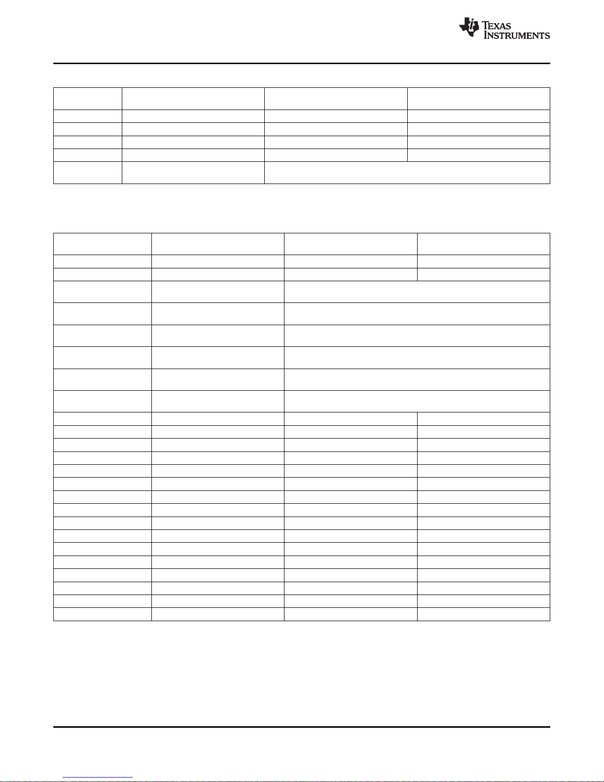
• Table 1 Summarizes Family Members
• For Complete Module Descriptions, See the
CC430 Family User's Guide (SLAU259)
Copyright © 2009–2013, Texas Instruments Incorporated
Page 2

ECCN 5E002 TSPA - Technology / Software Publicly Available
CC430F6137, CC430F6135, CC430F6127, CC430F6126, CC430F6125
CC430F5137, CC430F5135, CC430F5133
SLAS554H –MAY 2009–REVISED SEPTEMBER 2013
APPLICATIONS
• Wireless Analog and Digital Sensor Systems
• Heat Cost Allocators
• Thermostats
• AMR or AMI Metering
• Smart Grid Wireless Networks
DESCRIPTION
The Texas Instruments CC430 family of ultralow-power microcontroller system-on-chip (SoC) with integrated RF
transceiver cores consists of several devices featuring different sets of peripherals targeted for a wide range of
applications. The architecture, combined with five low-power modes, is optimized to achieve extended battery life
in portable measurement applications. The device features the powerful MSP430 16-bit RISC CPU, 16-bit
registers, and constant generators that contribute to maximum code efficiency.
The CC430 family provides a tight integration between the microcontroller core, its peripherals, software, and the
RF transceiver, making these true SoC solutions easy to use as well as improving performance.
The CC430F61xx series are microcontroller SoC configurations that combine the excellent performance of the
state-of-the-art CC1101 sub-1-GHz RF transceiver with the MSP430 CPUXV2, up to 32KB of in-system
programmable flash memory, up to 4KB of RAM, two 16-bit timers, a high-performance 12-bit analog-to-digital
converter (ADC) with eight external inputs plus internal temperature and battery sensors on CC430F613x
devices, a comparator, universal serial communication interfaces (USCIs), a 128-bit AES security accelerator, a
hardware multiplier, a DMA, a real-time clock (RTC) module with alarm capabilities, an LCD driver, and up to
44 I/O pins.
The CC430F513x series are microcontroller SoC configurations that combine the excellent performance of the
state-of-the-art CC1101 sub-1-GHz RF transceiver with the MSP430 CPUXV2, up to 32KB of in-system
programmable flash memory, up to 4KB of RAM, two 16-bit timers, a high performance 12-bit ADC with six
external inputs plus internal temperature and battery sensors, a comparator, universal serial communication
interfaces (USCIs), a 128-bit AES security accelerator, a hardware multiplier, a DMA, an RTC module with alarm
capabilities, and up to 30 I/O pins.
Typical applications for these devices include wireless analog and digital sensor systems, heat cost allocators,
thermostats, metering (AMR or AMI), and smart grid wireless networks.
www.ti.com
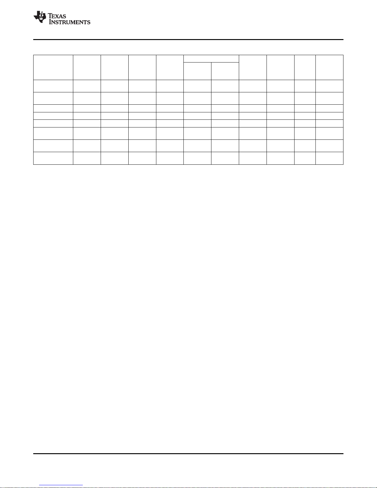
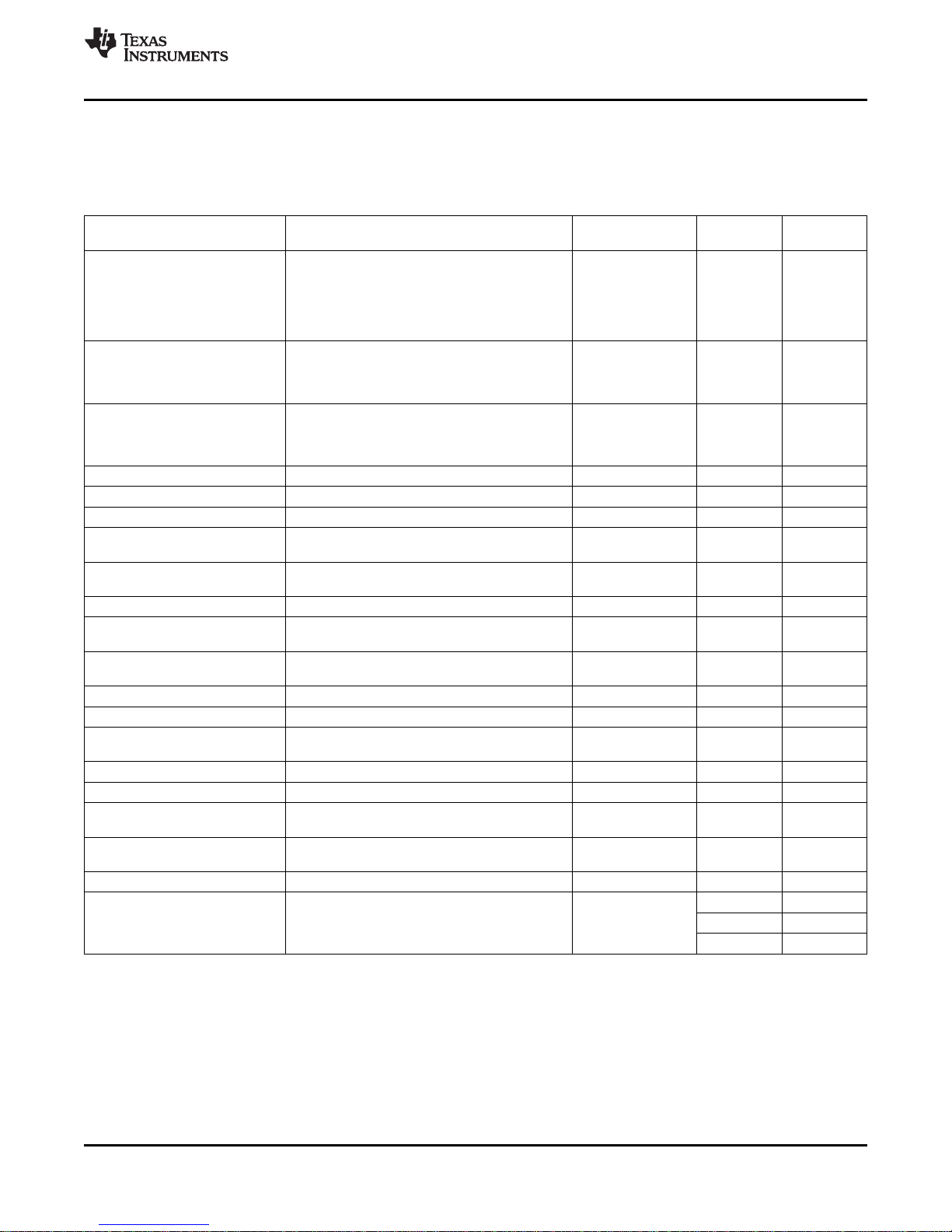
Table 1 summarizes the available family members.
For complete module descriptions, see the CC430 Family User's Guide (SLAU259).
2 Submit Documentation Feedback Copyright © 2009–2013, Texas Instruments Incorporated
Product Folder Links: CC430F6137 CC430F6135 CC430F6127 CC430F6126 CC430F6125 CC430F5137
CC430F5135 CC430F5133
Page 3
ECCN 5E002 TSPA - Technology / Software Publicly Available
CC430F6137, CC430F6135, CC430F6127, CC430F6126, CC430F6125
CC430F5137, CC430F5135, CC430F5133
www.ti.com
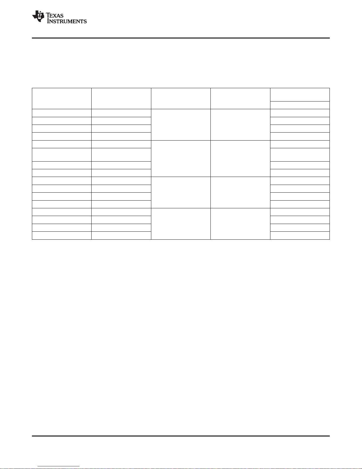
Table 1. Family Members
USCI
Device SRAM (KB) Timer_A
CC430F6137 32 4 5, 3 96 seg 1 1 8 ch. 44 64 RGC
CC430F6135 16 2 5, 3 96 seg 1 1 8 ch. 44 64 RGC
CC430F6127 32 4 5, 3 96 seg 1 1 n/a 8 ch. 44 64 RGC
CC430F6126 32 2 5, 3 96 seg 1 1 n/a 8 ch. 44 64 RGC
CC430F6125 16 2 5, 3 96 seg 1 1 n/a 8 ch. 44 64 RGC
CC430F5137 32 4 5, 3 n/a 1 1 6 ch. 30 48 RGZ
CC430F5135 16 2 5, 3 n/a 1 1 6 ch. 30 48 RGZ
CC430F5133 8 2 5, 3 n/a 1 1 6 ch. 30 48 RGZ
Program Package
(KB) Type
(1) For the most current package and ordering information, see the Package Option Addendum at the end of this document, or see the TI
web site at www.ti.com.
(2) Package drawings, thermal data, and symbolization are available at www.ti.com/packaging.
(3) Each number in the sequence represents an instantiation of Timer_A with its associated number of capture compare registers and PWM
output generators available. For example, a number sequence of 5, 3 would represent two instantiations of Timer_A, the first
instantiation having 5 and the second instantiation having 3 capture compare registers and PWM output generators, respectively.
(4) n/a = not available
(3)
LCD_B
(4)
Channel A: Channel B:
UART, LIN,
IrDA, SPI
SPI, I2C
SLAS554H –MAY 2009–REVISED SEPTEMBER 2013
(1)(2)
8 ext,
4 int ch.
8 ext,
4 int ch.
6 ext,
4 int ch.
6 ext,
4 int ch.
6 ext,
4 int ch.
(4)
Comp_B I/O
ADC12_A
Copyright © 2009–2013, Texas Instruments Incorporated Submit Documentation Feedback 3
Product Folder Links: CC430F6137 CC430F6135 CC430F6127 CC430F6126 CC430F6125 CC430F5137
CC430F5135 CC430F5133
Page 4
RAM
4kB
2kB
Power
Mgmt
LDO
SVM/SVS
Brownout
SYS
TA0
5 CC
Registers
EEM
(S: 3+1)
RTC_A
Comp_B
Flash
32kB
16kB
SMCLK
ACLK
MDB
MAB
XOUTXIN
Spy-Bi-
Wire
CRC16
Bus
Cntrl
Logic
MAB
MDB
MAB
MDB
MCLK
USCI_A0
(UART,
IrDA, SPI)
USCI_B0
(SPI, I2C)
LCD_B
96
Segments
1,2,3,4
Mux
I/O Ports
P1/P2
2x8 I/Os
PA
1x16 I/Os
P1.x/P2.x
2x8
I/O Ports
P3/P4
2x8 I/Os
PB
1x16 I/Os
P3.x/P4.x
2x8
I/O Ports
P5
1x8 I/Os
P5.x
1x8
AES128
Security
En-/Decryption
RF_XOUTRF_XIN
RF_NRF_P
TA1
3 CC
Registers
MODEM
RF/ANALOG
TX & RX
Frequency
Synthesizer
CPU Interface
Packet
Handler
Digital RSSI
Carrier Sense
PQI / LQI
CCA
Sub-1GHz
Radio
(CC1101)
MPY32
ADC12
(32kHz) (26MHz)
Unified
Clock
System
CPUXV2
incl. 16
Registers
JTAG
Interface
DMA
Controller
3 Channel
Port
Mapping
Controller
Watch-
dog
REF
Voltage
Reference
ECCN 5E002 TSPA - Technology / Software Publicly Available
CC430F6137, CC430F6135, CC430F6127, CC430F6126, CC430F6125
CC430F5137, CC430F5135, CC430F5133
SLAS554H –MAY 2009–REVISED SEPTEMBER 2013
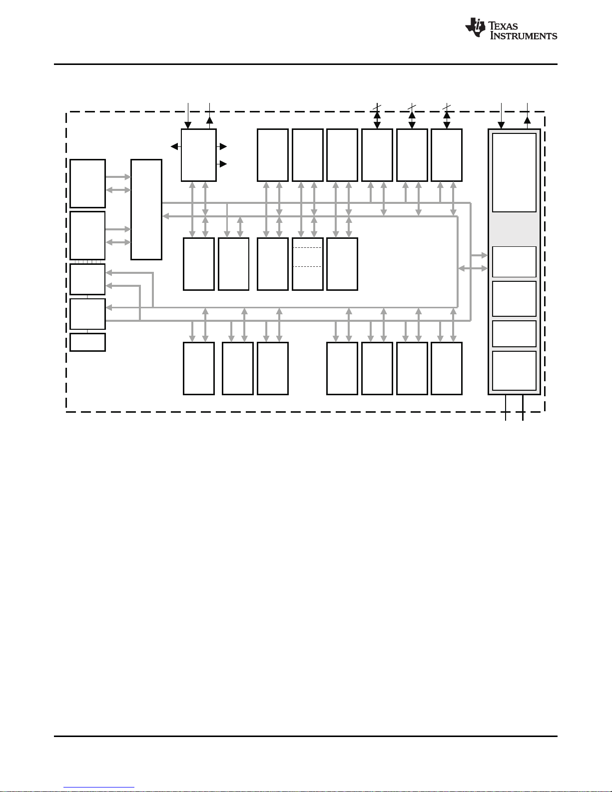
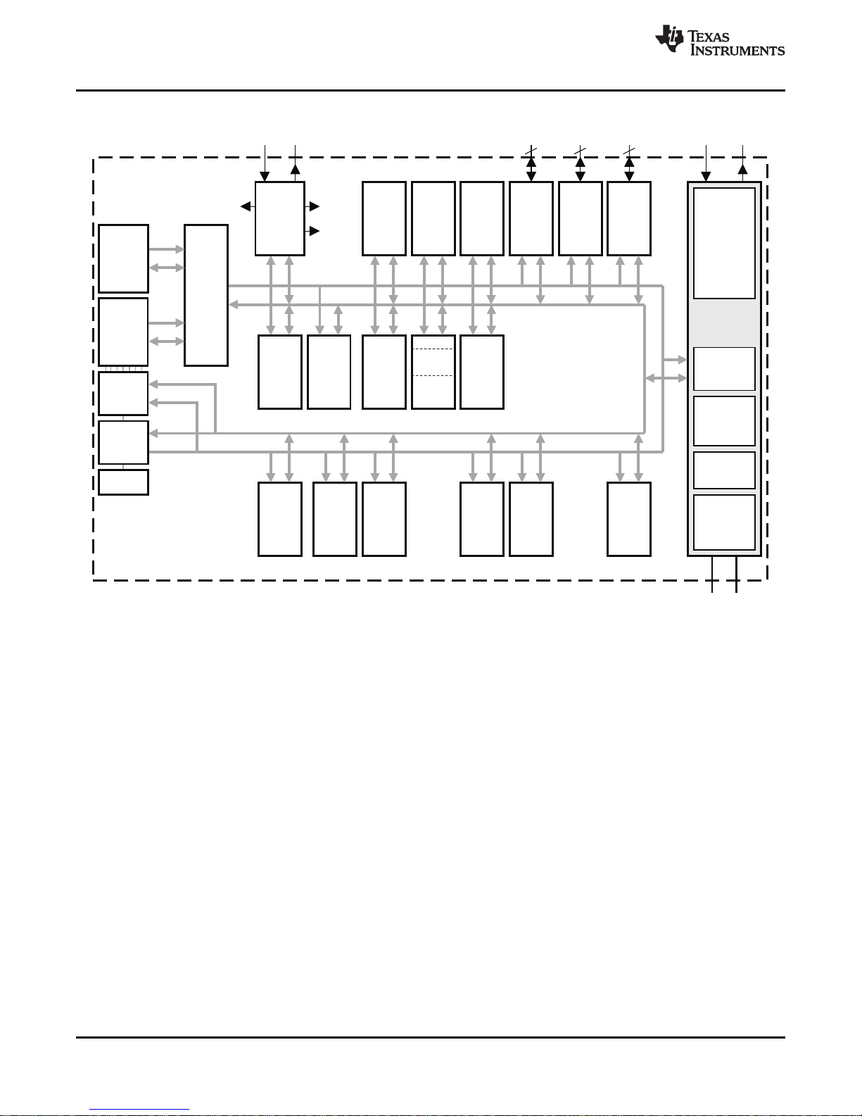
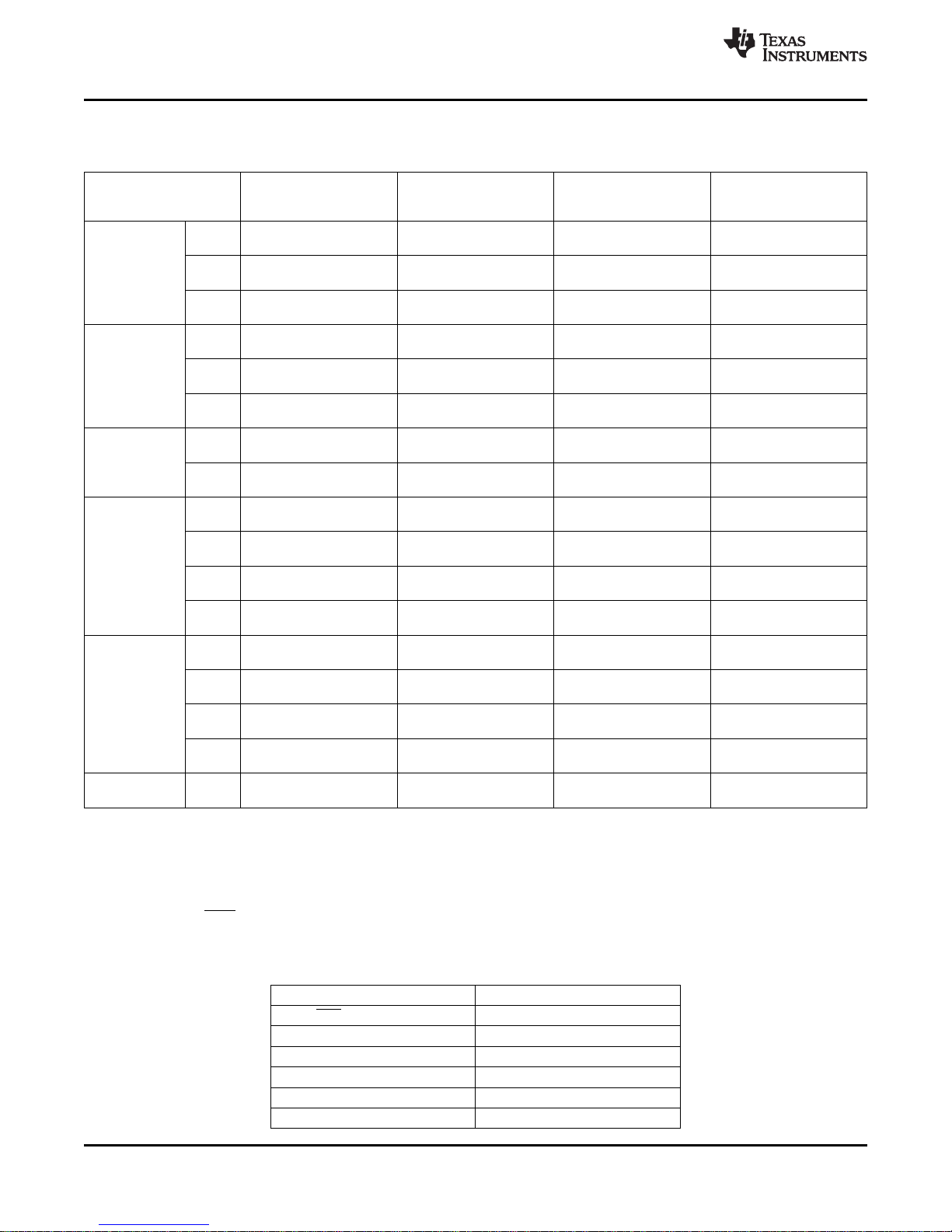
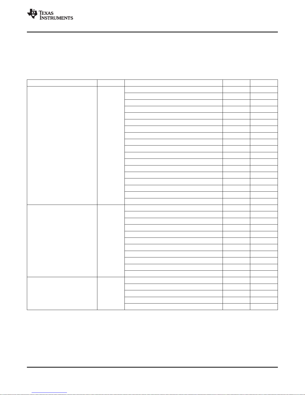
CC430F613x Functional Block Diagram
www.ti.com
4 Submit Documentation Feedback Copyright © 2009–2013, Texas Instruments Incorporated
Product Folder Links: CC430F6137 CC430F6135 CC430F6127 CC430F6126 CC430F6125 CC430F5137
CC430F5135 CC430F5133
Page 5

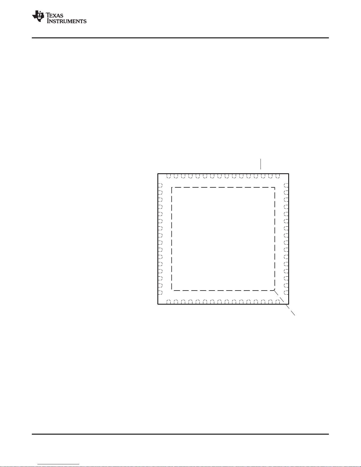
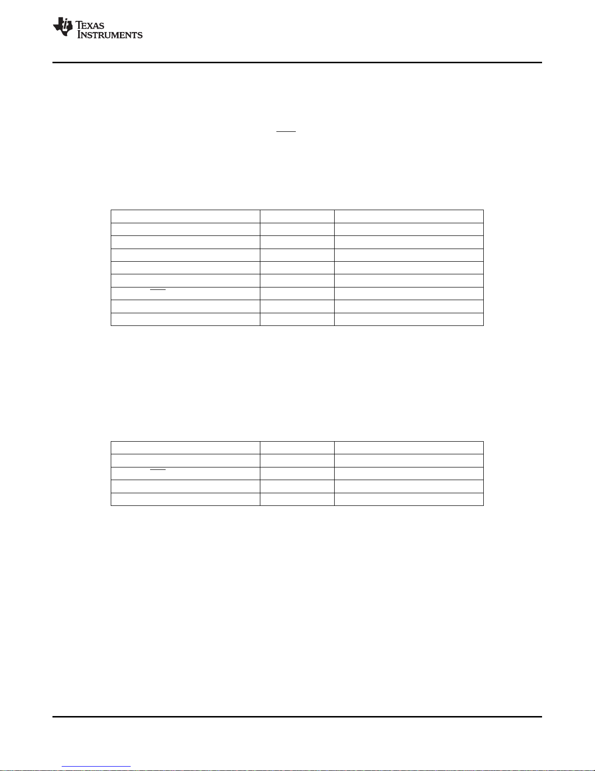
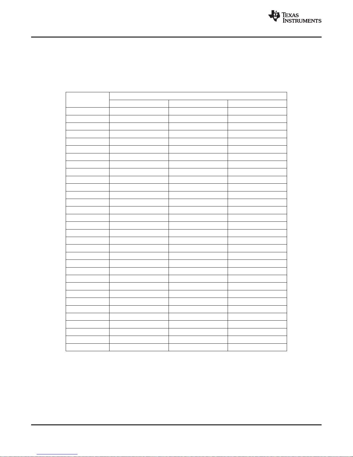
RGC PACKAGE
(TOP VIEW)
CC430F613x
P3.7/PM_SMCLK/S17
P2.0/PM_CBOUT1/PM_TA1CLK/CB0/A0
17
64
P3.6/PM_RFGDO1/S16
P2.1/PM_TA1CCR0A/CB1/A1
18
63
P3.5/PM_TA0CCR4A/S15
P2.2/PM_TA1CCR1A/CB2/A2
19
62
P2.3/PM_TA1CCR2A/CB3/A3
P3.4/PM_TA0CCR3A/S14
20
61
P2.4/PM_RTCCLK/CB4/A4/VREF-/VeREF-
P3.3/PM_TA0CCR2A/S13
21
60
P2.5/ /CB5/A5PM_SVMOUT /VREF+/VeREF+
P3.2/PM_TA0CCR1A/S12
22
59
DVCC
P4.4/S6
29
52
RST/NMI/SBWTDIO
P4.3/S5
30
51
TEST/SBWTCK
P4.2/S4
31
50
PJ.3/TCK
P4.1/S3
32
49
P2.6/PM_ACLK/CB6/A6
P3.1/PM_TA0CCR0A/S11
23
58
P2.7/ /CB7/A7PM_ADC12CLK/PM_DMAE0
P3.0/PM_CBOUT0/PM_TA0CLK/S10
24
57
AVCC
DVCC
25
56
P5.0/XIN
P4.7/S9
26
55
P5.1/XOUT
P4.6/S8
27
54
AVSS
P4.5/S7
28
53
P4.0/S2P1.0/PM_RFGDO0/S18
3316
P5.3/S1
P1.1/PM_RFGDO2/S19
3415
P5.2/S0
P1.2/PM_UCB0SOMI/PM_UCB0SCL/S20
35
14
RF_XINP1.3/PM_UCB0SIMO/PM_UCB0SDA/S21
3613
RF_XOUTP1.4/PM_UCB0CLK/PM_UCA0STE/S22
37
12
AVCC_RFDVCC
38
11
GUARD
LCDCAP/R33
45
4
PJ.0/TDO
P1.5/PM_UCA0RXD/PM_UCA0SOMI/R23
463
PJ.1/TDI/TCLK
P1.6/PM_UCA0TXD/PM_UCA0SIMO/R13/LCDREF
472
PJ.2/TMS
P1.7/PM_UCA0CLK/PM_UCB0STE/R03
48
1
AVCC_RF
VCORE
3910
RF_P
P5.4/S23
409
RF_NP5.5/COM3/S24
41
8
AVCC_RFP5.6/COM2/S25
42
7
AVCC_RF
P5.7/COM1/S26
436
R_BIAS
COM0
44
5
VSS
Exposed die
attached pad
www.ti.com
ECCN 5E002 TSPA - Technology / Software Publicly Available
CC430F6137, CC430F6135, CC430F6127, CC430F6126, CC430F6125
CC430F5137, CC430F5135, CC430F5133
SLAS554H –MAY 2009–REVISED SEPTEMBER 2013
NOTE: The secondary digital functions on ports P1, P2, and P3 are fully mappable. This pinout shows only the default
mapping. See Table 9 for details.
CAUTION: The LCDCAP/R33 must be connected to VSS if not used.
Copyright © 2009–2013, Texas Instruments Incorporated Submit Documentation Feedback 5
Product Folder Links: CC430F6137 CC430F6135 CC430F6127 CC430F6126 CC430F6125 CC430F5137
CC430F5135 CC430F5133
Page 6
RAM
4kB
2kB
2kB
Power
Mgmt
LDO
SVM/SVS
Brownout
TA0
5 CC
Registers
EEM
(S: 3+1)
RTC_A
Comp_B
Flash
32kB
32kB
16kB
SMCLK
ACLK
MDB
MAB
XOUTXIN
Spy-Bi-
Wire
CRC16
Bus
Cntrl
Logic
MAB
MDB
MAB
MDB
MCLK
USCI_A0
(UART,
IrDA, SPI)
USCI_B0
(SPI, I2C)
LCD_B
96
Segments
1,2,3,4
Mux
I/O Ports
P1/P2
2x8 I/Os
PA
1x16 I/Os
P1.x/P2.x
2x8
I/O Ports
P3/P4
2x8 I/Os
PB
1x16 I/Os
P3.x/P4.x
2x8
I/O Ports
P5
1x8 I/Os
P5.x
1x8
AES128
Security
En-/Decryption
RF_XOUTRF_XIN
RF_NRF_P
TA1
3 CC
Registers
MODEM
RF/ANALOG
TX & RX
Frequency
Synthesizer
CPU Interface
Packet
Handler
Digital RSSI
Carrier Sense
PQI / LQI
CCA
Sub-1GHz
Radio
(CC1101)
MPY32
(32kHz) (26MHz)
Unified
Clock
System
JTAG
Interface
DMA
Controller
3 Channel
SYS
Port
Mapping
Controller
Watch-
dog
REF
Voltage
Reference
CPUXV2
incl. 16
Registers
ECCN 5E002 TSPA - Technology / Software Publicly Available
CC430F6137, CC430F6135, CC430F6127, CC430F6126, CC430F6125
CC430F5137, CC430F5135, CC430F5133
SLAS554H –MAY 2009–REVISED SEPTEMBER 2013
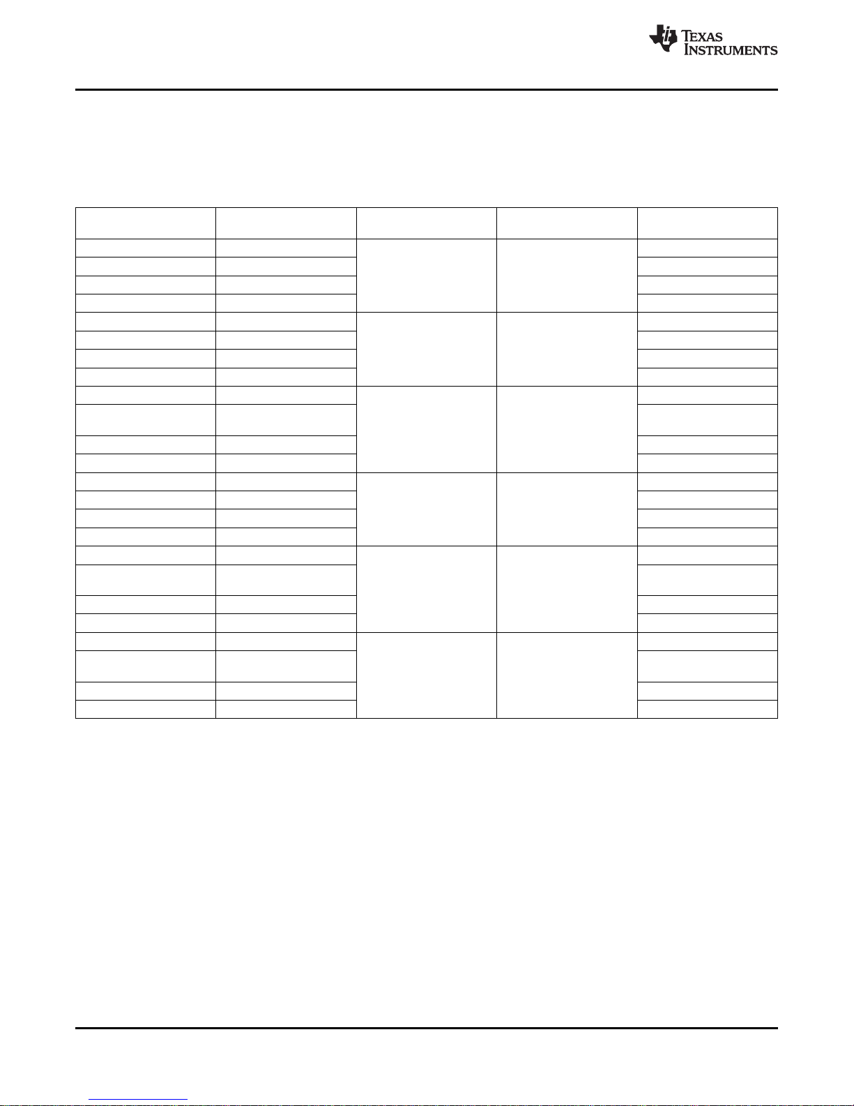
CC430F612x Functional Block Diagram
www.ti.com
6 Submit Documentation Feedback Copyright © 2009–2013, Texas Instruments Incorporated
Product Folder Links: CC430F6137 CC430F6135 CC430F6127 CC430F6126 CC430F6125 CC430F5137
CC430F5135 CC430F5133
Page 7
RGC PACKAGE
(TOP VIEW)
CC430F612x
P3.7/PM_SMCLK/S17
P2.0/PM_CBOUT1/PM_TA1CLK/CB0
17
64
P3.6/PM_RFGDO1/S16
P2.1/PM_TA1CCR0A/CB1
18
63
P3.5/PM_TA0CCR4A/S15
P2.2/PM_TA1CCR1A/CB2
19
62
P2.3/PM_TA1CCR2A/CB3
P3.4/PM_TA0CCR3A/S14
20
61
P2.4/PM_RTCCLK/CB4
P3.3/PM_TA0CCR2A/S13
21
60
P2.5/ /CB5PM_SVMOUT
P3.2/PM_TA0CCR1A/S12
22
59
DVCC
P4.4/S6
29
52
RST/NMI/SBWTDIO
P4.3/S5
30
51
TEST/SBWTCK
P4.2/S4
31
50
PJ.3/TCK
P4.1/S3
32
49
P2.6/PM_ACLK/CB6
P3.1/PM_TA0CCR0A/S11
23
58
P2.7/ /CB7PM_DMAE0
P3.0/PM_CBOUT0/PM_TA0CLK/S10
24
57
AVCC
DVCC
25
56
P5.0/XIN
P4.7/S9
26
55
P5.1/XOUT
P4.6/S8
27
54
AVSS
P4.5/S7
28
53
P4.0/S2P1.0/PM_RFGDO0/S18
3316
P5.3/S1
P1.1/PM_RFGDO2/S19
3415
P5.2/S0
P1.2/PM_UCB0SOMI/PM_UCB0SCL/S20
35
14
RF_XINP1.3/PM_UCB0SIMO/PM_UCB0SDA/S21
3613
RF_XOUTP1.4/PM_UCB0CLK/PM_UCA0STE/S22
37
12
AVCC_RFDVCC
38
11
GUARD
LCDCAP/R33
45
4
PJ.0/TDO
P1.5/PM_UCA0RXD/PM_UCA0SOMI/R23
463
PJ.1/TDI/TCLK
P1.6/PM_UCA0TXD/PM_UCA0SIMO/R13/LCDREF
472
PJ.2/TMS
P1.7/PM_UCA0CLK/PM_UCB0STE/R03
48
1
AVCC_RF
VCORE
3910
RF_P
P5.4/S23
409
RF_NP5.5/COM3/S24
41
8
AVCC_RFP5.6/COM2/S25
42
7
AVCC_RF
P5.7/COM1/S26
436
R_BIAS
COM0
44
5
VSS
Exposed die
attached pad
www.ti.com
ECCN 5E002 TSPA - Technology / Software Publicly Available
CC430F6137, CC430F6135, CC430F6127, CC430F6126, CC430F6125
CC430F5137, CC430F5135, CC430F5133
SLAS554H –MAY 2009–REVISED SEPTEMBER 2013
NOTE: The secondary digital functions on ports P1, P2, and P3 are fully mappable. This pinout shows only the default
mapping. See Table 9 for details.
CAUTION: The LCDCAP/R33 must be connected to VSS if not used.
Copyright © 2009–2013, Texas Instruments Incorporated Submit Documentation Feedback 7
Product Folder Links: CC430F6137 CC430F6135 CC430F6127 CC430F6126 CC430F6125 CC430F5137
CC430F5135 CC430F5133
Page 8
RAM
4kB
2kB
Power
Mgmt
LDO
SVM/SVS
Brownout
TA0
5 CC
Registers
EEM
(S: 3+1)
RTC_A
Comp_B
Flash
32
kB
16kB
8kB
SMCLK
ACLK
MDB
MAB
XOUTXIN
Spy-Bi-
Wire
CRC16
Bus
Cntrl
Logic
MAB
MDB
MAB
MDB
MCLK
USCI_A0
(UART,
IrDA, SPI)
USCI_B0
(SPI, I2C)
I/O Ports
P1/P2
2x8 I/Os
PA
1x16 I/Os
P1.x/P2.x
2x8
I/O Ports
P3
1x8 I/Os
P3.x
1x8
I/O Ports
P5
1x2 I/Os
P5.x
1x2
AES128
Security
En-/Decryption
RF_XOUTRF_XIN
RF_NRF_P
MODEM
RF/ANALOG
TX & RX
Frequency
Synthesizer
CPU Interface
Packet
Handler
Digital RSSI
Carrier Sense
PQI / LQI
CCA
Sub-1GHz
Radio
(CC1101)
MPY32
ADC12
(32kHz) (26MHz)
Unified
Clock
System
JTAG
Interface
DMA
Controller
3 Channel
SYS
Port
Mapping
Controller
Watch-
dog
REF
Voltage
Reference
CPUXV2
incl. 16
Registers
TA1
3 CC
Registers
ECCN 5E002 TSPA - Technology / Software Publicly Available
CC430F6137, CC430F6135, CC430F6127, CC430F6126, CC430F6125
CC430F5137, CC430F5135, CC430F5133
SLAS554H –MAY 2009–REVISED SEPTEMBER 2013
CC430F513x Functional Block Diagram
www.ti.com
8 Submit Documentation Feedback Copyright © 2009–2013, Texas Instruments Incorporated
Product Folder Links: CC430F6137 CC430F6135 CC430F6127 CC430F6126 CC430F6125 CC430F5137
CC430F5135 CC430F5133
Page 9
RGZ PACKAGE
(TOP VIEW)
12
11
4
3
2
1
10
9
8
7
6
5
13
14 15 16
17 181920
21 22
23
24
25
26
27
28
29
30
31
32
33
34
35
36
48
47 46 45
44 434241
40 39
38
37
P1.1/PM_RFGDO2
P1.2/PM_UCB0SOMI/PM_UCB0SCL
P1.7/PM_UCA0CLK/PM_UCB0STE
P2.0/PM_CBOUT1/PM_TA1CLK/CB0/A0
P2.1/PM_TA1CCR0A/CB1/A1
P2.2/PM_TA1CCR1A/CB2/A2
P1.3/PM_UCB0SIMO/PM_UCB0SDA
P1.4/PM_UCB0CLK/PM_UCA0STE
DVCC
VCORE
P1.5/PM_UCA0RXD/PM_UCA0SOMI
P1.6/PM_UCA0TXD/PM_UCA0SIMO
RF_XIN
RF_XOUT
AVCC_RF
GUARD
PJ.0/TDO
PJ.1/TDI/TCLK
AVCC_RF
RF_P
RF_N
AVCC_RF
AVCC_RF
R_BIAS
P2.3/PM_TA1CCR2A/CB3/A3
P2.4/PM_RTCCLK/CB4/A4/VREF-/VeREF-
RST/NMI/SBWTDIO
TEST/SBWTCK
PJ.3/TCK
PJ.2/TMS
P2.5/PM_SVMOUT/CB5/A5/VREF+/VeREF+
AVCC
P5.0/XIN
P5.1/XOUT
AVSS
DVCC
P1.0/PM_RFGDO0
P3.7/PM_SMCLK
P3.6/PM_RFGDO1
P3.5/PM_TA0CCR4A
P3.4/PM_TA0CCR3A
P3.3/PM_TA0CCR2A
P3.2/PM_TA0CCR1A
P3.1/PM_TA0CCR0A
P3.0/PM_CBOUT0/PM_TA0CLK
DVCC
P2.7/PM_ADC12CLK/PM_DMAE0
P2.6/PM_ACLK
VSS
Exposed die
attached pad
CC430F513x
www.ti.com
ECCN 5E002 TSPA - Technology / Software Publicly Available
CC430F6137, CC430F6135, CC430F6127, CC430F6126, CC430F6125
CC430F5137, CC430F5135, CC430F5133
SLAS554H –MAY 2009–REVISED SEPTEMBER 2013
NOTE: The secondary digital functions on ports P1, P2, and P3 are fully mappable. This pinout shows only the default
mapping. See Table 9 for details.
Copyright © 2009–2013, Texas Instruments Incorporated Submit Documentation Feedback 9
Product Folder Links: CC430F6137 CC430F6135 CC430F6127 CC430F6126 CC430F6125 CC430F5137
CC430F5135 CC430F5133
Page 10
ECCN 5E002 TSPA - Technology / Software Publicly Available
CC430F6137, CC430F6135, CC430F6127, CC430F6126, CC430F6125
CC430F5137, CC430F5135, CC430F5133
SLAS554H –MAY 2009–REVISED SEPTEMBER 2013
Table 2. CC430F613x and CC430F612x Terminal Functions
TERMINAL
NAME NO.
P1.7/ PM_UCA0CLK/
PM_UCB0STE/ R03
P1.6/ PM_UCA0TXD/ Default mapping: USCI_A0 UART transmit data; USCI_A0 SPI slave in master out
PM_UCA0SIMO/ R13/LCDREF Input/output port of third most positive analog LCD voltage (V3 or V4)
P1.5/ PM_UCA0RXD/
PM_UCA0SOMI/ R23
LCDCAP/ R33 4 I/O Input/output port of most positive analog LCD voltage (V1)
COM0 5 O LCD common output COM0 for LCD backplane
P5.7/ COM1/ S26 6 I/O LCD common output COM1 for LCD backplane
P5.6/ COM2/ S25 7 I/O LCD common output COM2 for LCD backplane
P5.5/ COM3/ S24 8 I/O LCD common output COM3 for LCD backplane
P5.4/ S23 9 I/O
VCORE 10 Regulated core power supply
DVCC 11 Digital power supply
P1.4/ PM_UCB0CLK/
PM_UCA0STE/ S22
P1.3/ PM_UCB0SIMO/
PM_UCB0SDA/ S21
P1.2/ PM_UCB0SOMI/
PM_UCB0SCL/ S20
P1.1/ PM_RFGDO2/ S19 15 I/O Default mapping: Radio GDO2 output
P1.0/ PM_RFGDO0/ S18 16 I/O Default mapping: Radio GDO0 output
P3.7/ PM_SMCLK/ S17 17 I/O Default mapping: SMCLK output
P3.6/ PM_RFGDO1/ S16 18 I/O Default mapping: Radio GDO1 output
P3.5/ PM_TA0CCR4A/ S15 19 I/O Default mapping: TA0 CCR4 compare output or capture input
P3.4/ PM_TA0CCR3A/ S14 20 I/O Default mapping: TA0 CCR3 compare output or capture input
P3.3/ PM_TA0CCR2A/ S13 21 I/O Default mapping: TA0 CCR2 compare output or capture input
1 I/O Default mapping: USCI_A0 clock input/output; USCI_B0 SPI slave transmit enable
2 I/O
3 I/O Default mapping: USCI_A0 UART receive data; USCI_A0 SPI slave out master in
12 I/O Default mapping: USCI_B0 clock input/output; USCI_A0 SPI slave transmit enable
13 I/O Default mapping: USCI_B0 SPI slave in master out; USCI_B0 I2C data
14 I/O Default mapping: USCI_B0 SPI slave out master in; UCSI_B0 I2C clock
(1)
I/O
General-purpose digital I/O with port interrupt and mappable secondary function
Input/output port of lowest analog LCD voltage (V5)
General-purpose digital I/O with port interrupt and mappable secondary function
External reference voltage input for regulated LCD voltage
General-purpose digital I/O with port interrupt and mappable secondary function
Input/output port of second most positive analog LCD voltage (V2)
LCD capacitor connection
CAUTION: Must be connected to VSS if not used.
General-purpose digital I/O
LCD segment output S26
General-purpose digital I/O
LCD segment output S25
General-purpose digital I/O
LCD segment output S24
General-purpose digital I/O
LCD segment output S23
General-purpose digital I/O with port interrupt and mappable secondary function
LCD segment output S22
General-purpose digital I/O with port interrupt and mappable secondary function
LCD segment output S21
General-purpose digital I/O with port interrupt and mappable secondary function
LCD segment output S20
General-purpose digital I/O with port interrupt and mappable secondary function
LCD segment output S19
General-purpose digital I/O with port interrupt and mappable secondary function
LCD segment output S18
General-purpose digital I/O with mappable secondary function
LCD segment output S17
General-purpose digital I/O with mappable secondary function
LCD segment output S16
General-purpose digital I/O with mappable secondary function
LCD segment output S15
General-purpose digital I/O with mappable secondary function
LCD segment output S14
General-purpose digital I/O with mappable secondary function
LCD segment output S13
DESCRIPTION
www.ti.com
(1) I = input, O = output
10 Submit Documentation Feedback Copyright © 2009–2013, Texas Instruments Incorporated
Product Folder Links: CC430F6137 CC430F6135 CC430F6127 CC430F6126 CC430F6125 CC430F5137
CC430F5135 CC430F5133
Page 11
ECCN 5E002 TSPA - Technology / Software Publicly Available
CC430F6137, CC430F6135, CC430F6127, CC430F6126, CC430F6125
CC430F5137, CC430F5135, CC430F5133
www.ti.com
Table 2. CC430F613x and CC430F612x Terminal Functions (continued)
TERMINAL
NAME NO.
P3.2/ PM_TA0CCR1A/ S12 22 I/O Default mapping: TA0 CCR1 compare output or capture input
P3.1/ PM_TA0CCR0A/ S11 23 I/O Default mapping: TA0 CCR0 compare output or capture input
P3.0/ PM_CBOUT0/PM_TA0CLK/
S10
DVCC 25 Digital power supply
P4.7/ S9 26 I/O
P4.6/ S8 27 I/O
P4.5/ S7 28 I/O
P4.4/ S6 29 I/O
P4.3/ S5 30 I/O
P4.2/ S4 31 I/O
P4.1/ S3 32 I/O
P4.0/ S2 33 I/O
P5.3/ S1 34 I/O
P5.2/ S0 35 I/O
RF_XIN 36 I Input terminal for RF crystal oscillator, or external clock input
RF_XOUT 37 O Output terminal for RF crystal oscillator
AVCC_RF 38 Radio analog power supply
AVCC_RF 39 Radio analog power supply
RF_P 40
RF_N 41
AVCC_RF 42 Radio analog power supply
AVCC_RF 43 Radio analog power supply
RBIAS 44 External bias resistor for radio reference current
GUARD 45 Power supply connection for digital noise isolation
PJ.0/ TDO 46 I/O
PJ.1/ TDI/ TCLK 47 I/O
PJ.2/ TMS 48 I/O
PJ.3/ TCK 49 I/O
TEST/ SBWTCK 50 I
24 I/O Default mapping: Comparator_B output; TA0 clock input
(1)
I/O
General-purpose digital I/O with mappable secondary function
LCD segment output S12
General-purpose digital I/O with mappable secondary function
LCD segment output S11
General-purpose digital I/O with mappable secondary function
LCD segment output S10
General-purpose digital I/O
LCD segment output S9
General-purpose digital I/O
LCD segment output S8
General-purpose digital I/O
LCD segment output S7
General-purpose digital I/O
LCD segment output S6
General-purpose digital I/O
LCD segment output S5
General-purpose digital I/O
LCD segment output S4
General-purpose digital I/O
LCD segment output S3
General-purpose digital I/O
LCD segment output S2
General-purpose digital I/O
LCD segment output S1
General-purpose digital I/O
LCD segment output S0
RF Positive RF input to LNA in receive mode
I/O Positive RF output from PA in transmit mode
RF Negative RF input to LNA in receive mode
I/O Negative RF output from PA in transmit mode
General-purpose digital I/O
Test data output port
General-purpose digital I/O
Test data input or test clock input
General-purpose digital I/O
Test mode select
General-purpose digital I/O
Test clock
Test mode pin – select digital I/O on JTAG pins
Spy-Bi-Wire input clock
SLAS554H –MAY 2009–REVISED SEPTEMBER 2013
DESCRIPTION
Copyright © 2009–2013, Texas Instruments Incorporated Submit Documentation Feedback 11
Product Folder Links: CC430F6137 CC430F6135 CC430F6127 CC430F6126 CC430F6125 CC430F5137
CC430F5135 CC430F5133
Page 12
ECCN 5E002 TSPA - Technology / Software Publicly Available
CC430F6137, CC430F6135, CC430F6127, CC430F6126, CC430F6125
CC430F5137, CC430F5135, CC430F5133
SLAS554H –MAY 2009–REVISED SEPTEMBER 2013
Table 2. CC430F613x and CC430F612x Terminal Functions (continued)
TERMINAL
NAME NO.
RST/NMI/ SBWTDIO 51 I/O Non-maskable interrupt input
DVCC 52 Digital power supply
AVSS 53 Analog ground supply for ADC12
P5.1/ XOUT 54 I/O
P5.0/ XIN 55 I/O
AVCC 56 Analog power supply
P2.7/ PM_ADC12CLK/ Default mapping: ADC12CLK output; DMA external trigger input
PM_DMAE0/ CB7 (/A7) Comparator_B input CB7
P2.6/ PM_ACLK/ CB6 (/A6) 58 I/O
P2.5/ PM_SVMOUT/ CB5 Comparator_B input CB5
(/A5/ VREF+/ VeREF+) Analog input A5 – 12-bit ADC (CC430F613x only)
P2.4/ PM_RTCCLK/ CB4 Comparator_B input CB4
(/A4/ VREF-/ VeREF-) Analog input A4 – 12-bit ADC (CC430F613x only)
P2.3/ PM_TA1CCR2A/ CB3 (/A3) 61 I/O
P2.2/ PM_TA1CCR1A/ CB2 (/A2) 62 I/O
P2.1/PM_TA1CCR0A/CB1(/A1) 63 I/O
P2.0/ PM_CBOUT1/ PM_TA1CLK/ Default mapping: Comparator_B output; TA1 clock input
CB0 (/A0) Comparator_B input CB0
VSS - Exposed die attach pad The exposed die attach pad must be connected to a solid ground plane as this is
57 I/O
59 I/O
60 I/O
64 I/O
(1)
I/O
Reset input active low
Spy-Bi-Wire data input/output
General-purpose digital I/O
Output terminal of crystal oscillator XT1
General-purpose digital I/O
Input terminal for crystal oscillator XT1
General-purpose digital I/O with port interrupt and mappable secondary function
Analog input A7 – 12-bit ADC (CC430F613x only)
General-purpose digital I/O with port interrupt and mappable secondary function
Default mapping: ACLK output
Comparator_B input CB6
Analog input A6 – 12-bit ADC (CC430F613x only)
General-purpose digital I/O with port interrupt and mappable secondary function
Default mapping: SVM output
Output of reference voltage to the ADC (CC430F613x only)
Input for an external reference voltage to the ADC (CC430F613x only)
General-purpose digital I/O with port interrupt and mappable secondary function
Default mapping: RTCCLK output
Negative terminal for the ADC's reference voltage for both sources, the internal
reference voltage, or an external applied reference voltage (CC430F613x only)
General-purpose digital I/O with port interrupt and mappable secondary function
Default mapping: TA1 CCR2 compare output or capture input
Comparator_B input CB3
Analog input A3 – 12-bit ADC (CC430F613x only)
General-purpose digital I/O with port interrupt and mappable secondary function
Default mapping: TA1 CCR1 compare output or capture input
Comparator_B input CB2
Analog input A2 – 12-bit ADC (CC430F613x only)
General-purpose digital I/O with port interrupt and mappable secondary function
Default mapping: TA1 CCR0 compare output or capture input
Comparator_B input CB1
Analog input A1 – 12-bit ADC (CC430F613x only)
General-purpose digital I/O with port interrupt and mappable secondary function
Analog input A0 – 12-bit ADC (CC430F613x only)
Ground supply
the ground connection for the chip.
DESCRIPTION
www.ti.com
12 Submit Documentation Feedback Copyright © 2009–2013, Texas Instruments Incorporated
Product Folder Links: CC430F6137 CC430F6135 CC430F6127 CC430F6126 CC430F6125 CC430F5137
CC430F5135 CC430F5133
Page 13
ECCN 5E002 TSPA - Technology / Software Publicly Available
CC430F6137, CC430F6135, CC430F6127, CC430F6126, CC430F6125
CC430F5137, CC430F5135, CC430F5133
www.ti.com
Table 3. CC430F513x Terminal Functions
TERMINAL
NAME NO.
P2.2/ PM_TA1CCR1A/ CB2/ A2 1 I/O
P2.1/ PM_TA1CCR0A/ CB1/ A1 2 I/O
P2.0/ PM_CBOUT1/ PM_TA1CLK/ Default mapping: Comparator_B output; TA1 clock input
CB0/ A0 Comparator_B input CB0
P1.7/ PM_UCA0CLK/ General-purpose digital I/O with port interrupt and mappable secondary function
PM_UCB0STE Default mapping: USCI_A0 clock input/output / USCI_B0 SPI slave transmit enable
P1.6/ PM_UCA0TXD/ General-purpose digital I/O with port interrupt and mappable secondary function
PM_UCA0SIMO Default mapping: USCI_A0 UART transmit data; USCI_A0 SPI slave in master out
P1.5/ PM_UCA0RXD/ General-purpose digital I/O with port interrupt and mappable secondary function
PM_UCA0SOMI Default mapping: USCI_A0 UART receive data; USCI_A0 SPI slave out master in
VCORE 7 Regulated core power supply
DVCC 8 Digital power supply
P1.4/ PM_UCB0CLK/ General-purpose digital I/O with port interrupt and mappable secondary function
PM_UCA0STE Default mapping: USCI_B0 clock input/output / USCI_A0 SPI slave transmit enable
P1.3/ PM_UCB0SIMO/ General-purpose digital I/O with port interrupt and mappable secondary function
PM_UCB0SDA Default mapping: USCI_B0 SPI slave in master out/USCI_B0 I2C data
P1.2/ PM_UCB0SOMI/ General-purpose digital I/O with port interrupt and mappable secondary function
PM_UCB0SCL Default mapping: USCI_B0 SPI slave out master in/UCSI_B0 I2C clock
P1.1/ PM_RFGDO2 12 I/O
P1.0/ PM_RFGDO0 13 I/O
P3.7/ PM_SMCLK 14 I/O
P3.6/ PM_RFGDO1 15 I/O
P3.5/ PM_TA0CCR4A 16 I/O
P3.4/ PM_TA0CCR3A 17 I/O
P3.3/ PM_TA0CCR2A 18 I/O
P3.2/ PM_TA0CCR1A 19 I/O
P3.1/ PM_TA0CCR0A 20 I/O
P3.0/ PM_CBOUT0/ PM_TA0CLK 21 I/O
DVCC 22 Digital power supply
P2.7/ PM_ADC12CLK/ General-purpose digital I/O with port interrupt and mappable secondary function
PM_DMAE0 Default mapping: ADC12CLK output; DMA external trigger input
P2.6/ PM_ACLK 24 I/O
RF_XIN 25 I Input terminal for RF crystal oscillator, or external clock input
RF_XOUT 26 O Output terminal for RF crystal oscillator
AVCC_RF 27 Radio analog power supply
3 I/O
4 I/O
5 I/O
6 I/O
9 I/O
10 I/O
11 I/O
23 I/O
(1)
I/O
General-purpose digital I/O with port interrupt and mappable secondary function
Default mapping: TA1 CCR1 compare output or capture input
Comparator_B input CB2
Analog input A2 – 12-bit ADC
General-purpose digital I/O with port interrupt and mappable secondary function
Default mapping: TA1 CCR0 compare output or capture input
Comparator_B input CB1
Analog input A1 – 12-bit ADC
General-purpose digital I/O with port interrupt and mappable secondary function
Analog input A0 – 12-bit ADC
General-purpose digital I/O with port interrupt and mappable secondary function
Default mapping: Radio GDO2 output
General-purpose digital I/O with port interrupt and mappable secondary function
Default mapping: Radio GDO0 output
General-purpose digital I/O with mappable secondary function
Default mapping: SMCLK output
General-purpose digital I/O with mappable secondary function
Default mapping: Radio GDO1 output
General-purpose digital I/O with mappable secondary function
Default mapping: TA0 CCR4 compare output or capture input
General-purpose digital I/O with mappable secondary function
Default mapping: TA0 CCR3 compare output or capture input
General-purpose digital I/O with mappable secondary function
Default mapping: TA0 CCR2 compare output or capture input
General-purpose digital I/O with mappable secondary function
Default mapping: TA0 CCR1 compare output or capture input
General-purpose digital I/O with mappable secondary function
Default mapping: TA0 CCR0 compare output or capture input
General-purpose digital I/O with mappable secondary function
Default mapping: Comparator_B output; TA0 clock input
General-purpose digital I/O with port interrupt and mappable secondary function
Default mapping: ACLK output
SLAS554H –MAY 2009–REVISED SEPTEMBER 2013
DESCRIPTION
(1) I = input, O = output
Copyright © 2009–2013, Texas Instruments Incorporated Submit Documentation Feedback 13
Product Folder Links: CC430F6137 CC430F6135 CC430F6127 CC430F6126 CC430F6125 CC430F5137
CC430F5135 CC430F5133
Page 14
ECCN 5E002 TSPA - Technology / Software Publicly Available
CC430F6137, CC430F6135, CC430F6127, CC430F6126, CC430F6125
CC430F5137, CC430F5135, CC430F5133
SLAS554H –MAY 2009–REVISED SEPTEMBER 2013
Table 3. CC430F513x Terminal Functions (continued)
TERMINAL
NAME NO.
AVCC_RF 28 Radio analog power supply
RF_P 29
RF_N 30
AVCC_RF 31 Radio analog power supply
AVCC_RF 32 Radio analog power supply
RBIAS 33 External bias resistor for radio reference current
GUARD 34 Power supply connection for digital noise isolation
PJ.0/ TDO 35 I/O
PJ.1/ TDI/ TCLK 36 I/O
PJ.2/ TMS 37 I/O
PJ.3/ TCK 38 I/O
TEST/ SBWTCK 39 I
RST/NMI/ SBWTDIO 40 I/O Non-maskable interrupt input
DVCC 41 Digital power supply
AVSS 42 Analog ground supply for ADC12
P5.1/ XOUT 43 I/O
P5.0/ XIN 44 I/O
AVCC 45 Analog power supply
P2.5/ PM_SVMOUT/ CB5/ Comparator_B input CB5
A5/ VREF+/ VeREF+ Analog input A5 – 12-bit ADC
P2.4/ PM_RTCCLK/ CB4/ Comparator_B input CB4
A4/ VREF-/ VeREF- Analog input A4 – 12-bit ADC
P2.3/ PM_TA1CCR2A/ CB3/ A3 48 I/O
VSS - Exposed die attach pad The exposed die attach pad must be connected to a solid ground plane as this is
46 I/O
47 I/O
(1)
I/O
RF Positive RF input to LNA in receive mode
I/O Positive RF output from PA in transmit mode
RF Negative RF input to LNA in receive mode
I/O Negative RF output from PA in transmit mode
General-purpose digital I/O
Test data output port
General-purpose digital I/O
Test data input or test clock input
General-purpose digital I/O
Test mode select
General-purpose digital I/O
Test clock
Test mode pin – select digital I/O on JTAG pins
Spy-Bi-Wire input clock
Reset input active low
Spy-Bi-Wire data input/output
General-purpose digital I/O
Output terminal of crystal oscillator XT1
General-purpose digital I/O
Input terminal for crystal oscillator XT1
General-purpose digital I/O with port interrupt and mappable secondary function
Default mapping: SVM output
Output of reference voltage to the ADC
Input for an external reference voltage to the ADC
General-purpose digital I/O with port interrupt and mappable secondary function
Default mapping: RTCCLK output
Negative terminal for the ADC's reference voltage for both sources, the internal
reference voltage, or an external applied reference voltage
General-purpose digital I/O with port interrupt and mappable secondary function
Default mapping: TA1 CCR2 compare output or capture input
Comparator_B input CB3
Analog input A3 – 12-bit ADC
Ground supply
the ground connection for the chip.
DESCRIPTION
www.ti.com
14 Submit Documentation Feedback Copyright © 2009–2013, Texas Instruments Incorporated
Product Folder Links: CC430F6137 CC430F6135 CC430F6127 CC430F6126 CC430F6125 CC430F5137
CC430F5135 CC430F5133
Page 15
BIAS
PA
RBIAS RF_XIN RF_XOUT
XOSC
LNA
0
90
FREQ
SYNTH
ADC
DEMODULATOR
PACKET HANDLER
RXFIFOTXFIFO
INTERFACE TO MCU
RADIOCONTROL
RF_P
RF_N
RCOSC
ADC
MODULATOR
ECCN 5E002 TSPA - Technology / Software Publicly Available
CC430F6137, CC430F6135, CC430F6127, CC430F6126, CC430F6125
CC430F5137, CC430F5135, CC430F5133
www.ti.com
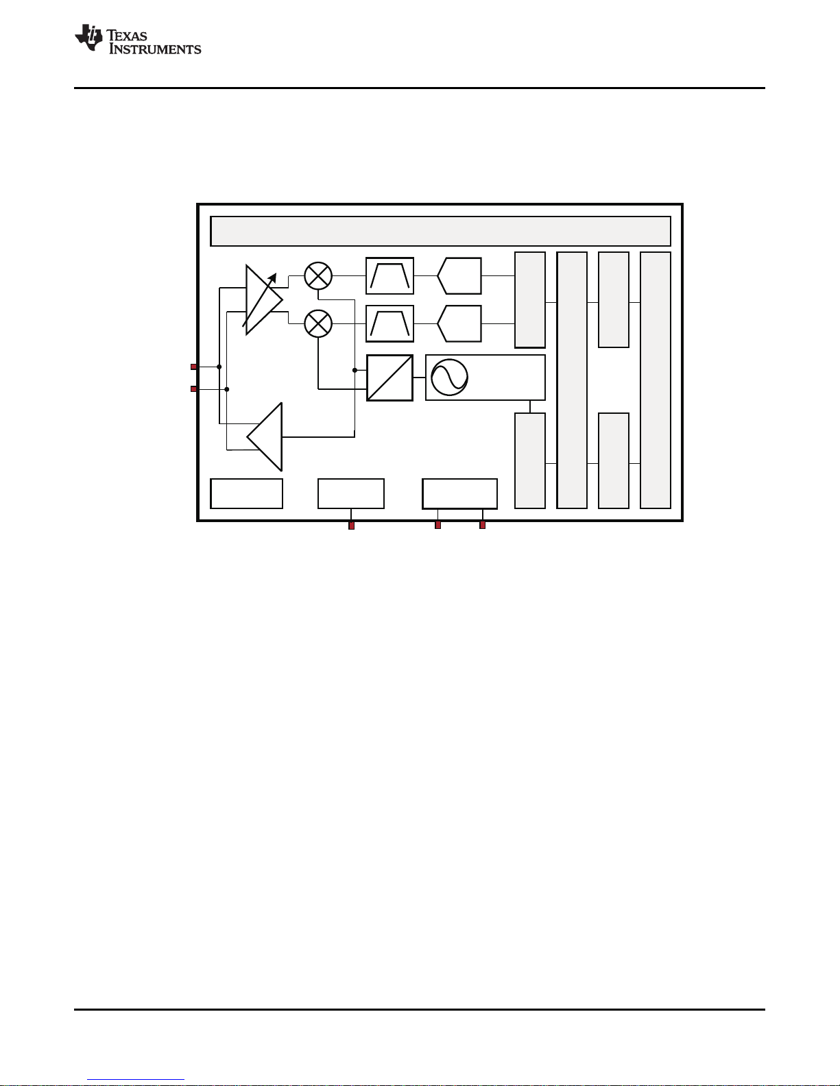
Short-Form Description
Sub-1-GHz Radio
The implemented sub-1-GHz radio module is based on the industry-leading CC1101, requiring very few external
components. Figure 1 shows a high-level block diagram of the implemented radio.
SLAS554H –MAY 2009–REVISED SEPTEMBER 2013
Figure 1. Sub-1-GHz Radio Block Diagram
The radio features a low-IF receiver. The received RF signal is amplified by a low-noise amplifier (LNA) and
down-converted in quadrature to the intermediate frequency (IF). At IF, the I/Q signals are digitized. Automatic
gain control (AGC), fine channel filtering, demodulation bit and packet synchronization are performed digitally.
The transmitter part is based on direct synthesis of the RF frequency. The frequency synthesizer includes a
completely on-chip LC VCO and a 90° phase shifter for generating the I and Q LO signals to the downconversion mixers in receive mode.
The 26-MHz crystal oscillator generates the reference frequency for the synthesizer, as well as clocks for the
ADC and the digital part.
A memory mapped register interface is used for data access, configuration, and status request by the CPU.
The digital baseband includes support for channel configuration, packet handling, and data buffering.
For complete module descriptions, see the CC430 Family User's Guide (SLAU259).
Copyright © 2009–2013, Texas Instruments Incorporated Submit Documentation Feedback 15
Product Folder Links: CC430F6137 CC430F6135 CC430F6127 CC430F6126 CC430F6125 CC430F5137
CC430F5135 CC430F5133
Page 16

ECCN 5E002 TSPA - Technology / Software Publicly Available
CC430F6137, CC430F6135, CC430F6127, CC430F6126, CC430F6125
CC430F5137, CC430F5135, CC430F5133
SLAS554H –MAY 2009–REVISED SEPTEMBER 2013
CPU
The MSP430 CPU has a 16-bit RISC architecture that is highly transparent to the application. All operations,
other than program-flow instructions, are performed as register operations in conjunction with seven addressing
modes for source operand and four addressing modes for destination operand.
The CPU is integrated with 16 registers that provide reduced instruction execution time. The register-to-register
operation execution time is one cycle of the CPU clock.
Four of the registers, R0 to R3, are dedicated as program counter, stack pointer, status register, and constant
generator, respectively. The remaining registers are general-purpose registers.
Peripherals are connected to the CPU using data, address, and control buses and can be handled with all
instructions.
The instruction set consists of the original 51 instructions with three formats and seven address modes and
additional instructions for the expanded address range. Each instruction can operate on word and byte data.
Operating Modes
The CC430 has one active mode and five software-selectable low-power modes of operation. An interrupt event
can wake up the device from any of the low-power modes, service the request, and restore back to the lowpower mode on return from the interrupt program.
The following six operating modes can be configured by software:
• Active mode (AM)
– All clocks are active
• Low-power mode 0 (LPM0)
– CPU is disabled
– ACLK and SMCLK remain active, MCLK is disabled
– FLL loop control remains active
• Low-power mode 1 (LPM1)
– CPU is disabled
– FLL loop control is disabled
– ACLK and SMCLK remain active, MCLK is disabled
• Low-power mode 2 (LPM2)
– CPU is disabled
– MCLK and FLL loop control and DCOCLK are disabled
– DCO's dc-generator remains enabled
– ACLK remains active
• Low-power mode 3 (LPM3)
– CPU is disabled
– MCLK, FLL loop control, and DCOCLK are disabled
– DCO's dc-generator is disabled
– ACLK remains active
• Low-power mode 4 (LPM4)
– CPU is disabled
– ACLK is disabled
– MCLK, FLL loop control, and DCOCLK are disabled
– DCO's dc-generator is disabled
– Crystal oscillator is stopped
– Complete data retention
www.ti.com
16 Submit Documentation Feedback Copyright © 2009–2013, Texas Instruments Incorporated
Product Folder Links: CC430F6137 CC430F6135 CC430F6127 CC430F6126 CC430F6125 CC430F5137
CC430F5135 CC430F5133
Page 17
ECCN 5E002 TSPA - Technology / Software Publicly Available
CC430F6137, CC430F6135, CC430F6127, CC430F6126, CC430F6125
CC430F5137, CC430F5135, CC430F5133
www.ti.com
Interrupt Vector Addresses
The interrupt vectors and the power-up start address are located in the address range 0FFFFh to 0FF80h. The
vector contains the 16-bit address of the appropriate interrupt-handler instruction sequence.
Table 4. Interrupt Sources, Flags, and Vectors
INTERRUPT SOURCE INTERRUPT FLAG PRIORITY
System Reset
Power-Up
External Reset
Watchdog Timeout, Password
WDTIFG, KEYV (SYSRSTIV)
Violation
Flash Memory Password Violation
System NMI
PMM
Vacant Memory Access
JTAG Mailbox
SVMLIFG, SVMHIFG, DLYLIFG, DLYHIFG,
VLRLIFG, VLRHIFG, VMAIFG, JMBNIFG, (Non)maskable 0FFFCh 62
JMBOUTIFG (SYSSNIV)
User NMI
NMI
Oscillator Fault
NMIIFG, OFIFG, ACCVIFG (SYSUNIV)
Flash Memory Access Violation
Comparator_B Comparator_B Interrupt Flags (CBIV)
Watchdog Interval Timer Mode WDTIFG Maskable 0FFF6h 59
USCI_A0 Receive or Transmit UCA0RXIFG, UCA0TXIFG (UCA0IV)
USCI_B0 Receive or Transmit Maskable 0FFF2h 57
ADC12_A
(Reserved on CC430F612x)
UCB0RXIFG, UCB0TXIFG, I2C Status Interrupt
Flags (UCB0IV)
ADC12IFG0 ... ADC12IFG15 (ADC12IV)
TA0 TA0CCR0 CCIFG0 Maskable 0FFEEh 55
TA0 Maskable 0FFECh 54
RF1A CC1101-based Radio Maskable 0FFEAh 53
TA0CCR1 CCIFG1 ... TA0CCR4 CCIFG4,
TA0IFG (TA0IV)
Radio Interface Interrupt Flags (RF1AIFIV)
Radio Core Interrupt Flags (RF1AIV)
DMA DMA0IFG, DMA1IFG, DMA2IFG (DMAIV)
TA1 TA1CCR0 CCIFG0 Maskable 0FFE6h 51
TA1 Maskable 0FFE4h 50
TA1CCR1 CCIFG1 ... TA1CCR2 CCIFG2,
TA1IFG (TA1IV)
I/O Port P1 P1IFG.0 to P1IFG.7 (P1IV)
I/O Port P2 P2IFG.0 to P2IFG.7 (P2IV)
(Reserved on CC430F513x)
LCD_B
RTC_A Maskable 0FFDCh 46
LCD_B Interrupt Flags (LCDBIV)
RTCRDYIFG, RTCTEVIFG, RTCAIFG,
RT0PSIFG, RT1PSIFG (RTCIV)
AES AESRDYIFG Maskable 0FFDAh 45
Reserved Reserved
(4)
(1) Multiple source flags
(2) A reset is generated if the CPU tries to fetch instructions from within peripheral space.
(3) (Non)maskable: the individual interrupt-enable bit can disable an interrupt event, but the general-interrupt enable cannot disable it.
(4) Reserved interrupt vectors at addresses are not used in this device and can be used for regular program code if necessary. To maintain
compatibility with other devices, it is recommended to reserve these locations.
(1)(2)
(1)(3)
(1)(3)
(1)
(1)
(1)
(1)
(1)
(1)
(1)
(1)
(1)
(1)
(1)
SLAS554H –MAY 2009–REVISED SEPTEMBER 2013
SYSTEM WORD
INTERRUPT ADDRESS
Reset 0FFFEh 63, highest
(Non)maskable 0FFFAh 61
Maskable 0FFF8h 60
Maskable 0FFF4h 58
Maskable 0FFF0h 56
Maskable 0FFE8h 52
Maskable 0FFE2h 49
Maskable 0FFE0h 48
Maskable 0FFDEh 47
0FFD8h 44
⋮ ⋮
0FF80h 0, lowest
Copyright © 2009–2013, Texas Instruments Incorporated Submit Documentation Feedback 17
Product Folder Links: CC430F6137 CC430F6135 CC430F6127 CC430F6126 CC430F6125 CC430F5137
CC430F5135 CC430F5133
Page 18
ECCN 5E002 TSPA - Technology / Software Publicly Available
CC430F6137, CC430F6135, CC430F6127, CC430F6126, CC430F6125
CC430F5137, CC430F5135, CC430F5133
SLAS554H –MAY 2009–REVISED SEPTEMBER 2013
Memory Organization
Table 5. Memory Organization
CC430F6137 CC430F6135
CC430F6127 CC430F6126
CC430F5137
Main Memory Total 32kB 32kB 16kB 8kB
(flash) Size
Main: Interrupt 00FFFFh to 00FF80h 00FFFFh to 00FF80h 00FFFFh to 00FF80h 00FFFFh to 00FF80h
vector
Main: code Bank 0 32kB 32kB 16kB 8kB
memory 00FFFFh to 008000h 00FFFFh to 008000h 00FFFFh to 00C000h 00FFFFh to 00E000h
RAM
Device
Descriptor
Information
memory (flash)
Bootstrap loader
(BSL) memory
(flash)
Peripherals
(1) All memory regions not specified here are vacant memory, and any access to them causes a Vacant Memory Interrupt.
Total 4kB 2kB 2kB 2kB
Size
Sect 1 2kB not available not available not available
002BFFh to 002400h
Sect 0 2kB 2kB 2kB 2kB
0023FFh to 001C00h 0023FFh to 001C00h 0023FFh to 001C00h 0023FFh to 001C00h
128 B 128 B 128 B 128 B
001AFFh to 001A80h 001AFFh to 001A80h 001AFFh to 001A80h 001AFFh to 001A80h
128 B 128 B 128 B 128 B
001A7Fh to 001A00h 001A7Fh to 001A00h 001A7Fh to 001A00h 001A7Fh to 001A00h
Info A 128 B 128 B 128 B 128 B
0019FFh to 001980h 0019FFh to 001980h 0019FFh to 001980h 0019FFh to 001980h
Info B 128 B 128 B 128 B 128 B
00197Fh to 001900h 00197Fh to 001900h 00197Fh to 001900h 00197Fh to 001900h
Info C 128 B 128 B 128 B 128 B
0018FFh to 001880h 0018FFh to 001880h 0018FFh to 001880h 0018FFh to 001880h
Info D 128 B 128 B 128 B 128 B
00187Fh to 001800h 00187Fh to 001800h 00187Fh to 001800h 00187Fh to 001800h
BSL 3 512 B 512 B 512 B 512 B
0017FFh to 001600h 0017FFh to 001600h 0017FFh to 001600h 0017FFh to 001600h
BSL 2 512 B 512 B 512 B 512 B
0015FFh to 001400h 0015FFh to 001400h 0015FFh to 001400h 0015FFh to 001400h
BSL 1 512 B 512 B 512 B 512 B
0013FFh to 001200h 0013FFh to 001200h 0013FFh to 001200h 0013FFh to 001200h
BSL 0 512 B 512 B 512 B 512 B
0011FFh to 001000h 0011FFh to 001000h 0011FFh to 001000h 0011FFh to 001000h
000FFFh to 0h 000FFFh to 0h 000FFFh to 0h 000FFFh to 0h
(1)
4 KB 4 KB 4 KB 4 KB
(1)
CC430F6125 CC430F5133
CC430F5135
(1)
www.ti.com
(1)
Bootstrap Loader (BSL)
The BSL enables users to program the flash memory or RAM using various serial interfaces. Access to the
device memory via the BSL is protected by an user-defined password. BSL entry requires a specific entry
sequence on the RST/NMI/SBWTDIO and TEST/SBWTCK pins. For a complete description of the features of the
BSL and its implementation, see the MSP430 Programming Via the Bootstrap Loader User's Guide (SLAU319).
Table 6. UART BSL Pin Requirements and Functions
RST/NMI/SBWTDIO Entry sequence signal
18 Submit Documentation Feedback Copyright © 2009–2013, Texas Instruments Incorporated
Product Folder Links: CC430F6137 CC430F6135 CC430F6127 CC430F6126 CC430F6125 CC430F5137
DEVICE SIGNAL BSL FUNCTION
TEST/SBWTCK Entry sequence signal
P1.6 Data transmit
P1.5 Data receive
VCC Power supply
VSS Ground supply
CC430F5135 CC430F5133
Page 19
ECCN 5E002 TSPA - Technology / Software Publicly Available
CC430F6137, CC430F6135, CC430F6127, CC430F6126, CC430F6125
CC430F5137, CC430F5135, CC430F5133
www.ti.com
JTAG Operation
JTAG Standard Interface
The CC430 family supports the standard JTAG interface which requires four signals for sending and receiving
data. The JTAG signals are shared with general-purpose I/O. The TEST/SBWTCK pin is used to enable the
JTAG signals. In addition to these signals, the RST/NMI/SBWTDIO is required to interface with MSP430
development tools and device programmers. The JTAG pin requirements are shown in Table 7. For further
details on interfacing to development tools and device programmers, see the MSP430 Hardware Tools User's
Guide (SLAU278). For a complete description of the features of the JTAG interface and its implementation, see
MSP430 Programming Via the JTAG Interface (SLAU320).
Table 7. JTAG Pin Requirements and Functions
DEVICE SIGNAL DIRECTION FUNCTION
PJ.3/TCK IN JTAG clock input
PJ.2/TMS IN JTAG state control
PJ.1/TDI/TCLK IN JTAG data input, TCLK input
PJ.0/TDO OUT JTAG data output
TEST/SBWTCK IN Enable JTAG pins
RST/NMI/SBWTDIO IN External reset
VCC Power supply
VSS Ground supply
SLAS554H –MAY 2009–REVISED SEPTEMBER 2013
Spy-Bi-Wire Interface
In addition to the standard JTAG interface, the CC430 family supports the two wire Spy-Bi-Wire interface. Spy-BiWire can be used to interface with MSP430 development tools and device programmers. The Spy-Bi-Wire
interface pin requirements are shown in Table 8. For further details on interfacing to development tools and
device programmers, see the MSP430 Hardware Tools User's Guide (SLAU278). For a complete description of
the features of the JTAG interface and its implementation, see MSP430 Programming Via the JTAG Interface
(SLAU320).
Table 8. Spy-Bi-Wire Pin Requirements and Functions
DEVICE SIGNAL DIRECTION FUNCTION
TEST/SBWTCK IN Spy-Bi-Wire clock input
RST/NMI/SBWTDIO IN, OUT Spy-Bi-Wire data input/output
VCC Power supply
VSS Ground supply
Flash Memory
The flash memory can be programmed via the JTAG port, Spy-Bi-Wire (SBW), or in-system by the CPU. The
CPU can perform single-byte, single-word, and long-word writes to the flash memory. Features of the flash
memory include:
• Flash memory has n segments of main memory and four segments of information memory (Info A to Info D)
of 128 bytes each. Each segment in main memory is 512 bytes in size.
• Segments 0 to n may be erased in one step, or each segment may be individually erased.
• Segments Info A to Info D can be erased individually, or as a group with the main memory segments.
Segments Info A to Info D are also called information memory.
• Segment A can be locked separately.
Copyright © 2009–2013, Texas Instruments Incorporated Submit Documentation Feedback 19
Product Folder Links: CC430F6137 CC430F6135 CC430F6127 CC430F6126 CC430F6125 CC430F5137
CC430F5135 CC430F5133
Page 20

ECCN 5E002 TSPA - Technology / Software Publicly Available
CC430F6137, CC430F6135, CC430F6127, CC430F6126, CC430F6125
CC430F5137, CC430F5135, CC430F5133
SLAS554H –MAY 2009–REVISED SEPTEMBER 2013
RAM Memory
The RAM memory is made up of n sectors. Each sector can be completely powered down to save leakage,
however, all data is lost. Features of the RAM memory include:
• RAM memory has n sectors of 2k bytes each.
• Each sector 0 to n can be complete disabled, however data retention is lost.
• Each sector 0 to n automatically enters low power retention mode when possible.
Peripherals
Peripherals are connected to the CPU through data, address, and control busses and can be handled using all
instructions. For complete module descriptions, see the CC430 Family User's Guide (SLAU259).
Oscillator and System Clock
The Unified Clock System (UCS) module includes support for a 32768-Hz watch crystal oscillator, an internal
very-low-power low-frequency oscillator (VLO), an internal trimmed low-frequency oscillator (REFO), an
integrated internal digitally-controlled oscillator (DCO), and a high-frequency crystal oscillator. The UCS module
is designed to meet the requirements of both low system cost and low-power consumption. The UCS module
features digital frequency locked loop (FLL) hardware that, in conjunction with a digital modulator, stabilizes the
DCO frequency to a programmable multiple of the watch crystal frequency. The internal DCO provides a fast
turn-on clock source and stabilizes in less than 5 µs. The UCS module provides the following clock signals:
• Auxiliary clock (ACLK), sourced from a 32768-Hz watch crystal, a high-frequency crystal, the internal lowfrequency oscillator (VLO), or the trimmed low-frequency oscillator (REFO).
• Main clock (MCLK), the system clock used by the CPU. MCLK can be sourced by same sources made
available to ACLK.
• Sub-Main clock (SMCLK), the subsystem clock used by the peripheral modules. SMCLK can be sourced by
same sources made available to ACLK.
• ACLK/n, the buffered output of ACLK, ACLK/2, ACLK/4, ACLK/8, ACLK/16, ACLK/32.
www.ti.com
Power Management Module (PMM)
The PMM includes an integrated voltage regulator that supplies the core voltage to the device and contains
programmable output levels to provide for power optimization. The PMM also includes supply voltage supervisor
(SVS) and supply voltage monitoring (SVM) circuitry, as well as brownout protection. The brownout circuit is
implemented to provide the proper internal reset signal to the device during power-on and power-off. The
SVS/SVM circuitry detects if the supply voltage drops below a user-selectable level and supports both supply
voltage supervision (the device is automatically reset) and supply voltage monitoring (SVM, the device is not
automatically reset). SVS and SVM circuitry is available on the primary supply and core supply.
Digital I/O
There are up to five 8-bit I/O ports implemented: ports P1 through P5.
• All individual I/O bits are independently programmable.
• Any combination of input, output, and interrupt conditions is possible.
• Programmable pullup or pulldown on all ports.
• Programmable drive strength on all ports.
• Edge-selectable interrupt input capability for all the eight bits of ports P1 and P2.
• Read/write access to port-control registers is supported by all instructions.
• Ports can be accessed byte-wise (P1 through P5) or word-wise in pairs (PA and PB).
20 Submit Documentation Feedback Copyright © 2009–2013, Texas Instruments Incorporated
Product Folder Links: CC430F6137 CC430F6135 CC430F6127 CC430F6126 CC430F6125 CC430F5137
CC430F5135 CC430F5133
Page 21
ECCN 5E002 TSPA - Technology / Software Publicly Available
CC430F6137, CC430F6135, CC430F6127, CC430F6126, CC430F6125
CC430F5137, CC430F5135, CC430F5133
www.ti.com
Port Mapping Controller
The port mapping controller allows the flexible and re-configurable mapping of digital functions to port pins of
ports P1 through P3.
Table 9. Port Mapping, Mnemonics and Functions
VALUE PxMAPy MNEMONIC INPUT PIN FUNCTION (PxDIR.y = 0)
0 PM_NONE None DVSS
(1)
1
(1)
2
3 PM_ACLK None ACLK output
4 PM_MCLK None MCLK output
5 PM_SMCLK None SMCLK output
6 PM_RTCCLK None RTCCLK output
(1)
7
8 PM_SVMOUT None SVM output
9 PM_TA0CCR0A TA0 CCR0 capture input CCI0A TA0 CCR0 compare output Out0
10 PM_TA0CCR1A TA0 CCR1 capture input CCI1A TA0 CCR1 compare output Out1
11 PM_TA0CCR2A TA0 CCR2 capture input CCI2A TA0 CCR2 compare output Out2
12 PM_TA0CCR3A TA0 CCR3 capture input CCI3A TA0 CCR3 compare output Out3
13 PM_TA0CCR4A TA0 CCR4 capture input CCI4A TA0 CCR4 compare output Out4
14 PM_TA1CCR0A TA1 CCR0 capture input CCI0A TA1 CCR0 compare output Out0
15 PM_TA1CCR1A TA1 CCR1 capture input CCI1A TA1 CCR1 compare output Out1
16 PM_TA1CCR2A TA1 CCR2 capture input CCI2A TA1 CCR2 compare output Out2
(2)
17
(2)
18
(3)
19
(4)
20
(4)
21
(5)
22
23 PM_RFGDO0 Radio GDO0 (direction controlled by Radio)
24 PM_RFGDO1 Radio GDO1 (direction controlled by Radio)
25 PM_RFGDO2 Radio GDO2 (direction controlled by Radio)
26 Reserved None DVSS
PM_CBOUT0
PM_TA0CLK TA0 clock input -
PM_CBOUT1 -
PM_TA1CLK TA1 clock input -
PM_ADC12CLK - ADC12CLK output
PM_DMAE0 DMA external trigger input -
PM_UCA0RXD USCI_A0 UART RXD (Direction controlled by USCI - input)
PM_UCA0SOMI USCI_A0 SPI slave out master in (direction controlled by USCI)
PM_UCA0TXD USCI_A0 UART TXD (Direction controlled by USCI - output)
PM_UCA0SIMO USCI_A0 SPI slave in master out (direction controlled by USCI)
PM_UCA0CLK USCI_A0 clock input/output (direction controlled by USCI)
PM_UCB0STE USCI_B0 SPI slave transmit enable (direction controlled by USCI - input)
PM_UCB0SOMI USCI_B0 SPI slave out master in (direction controlled by USCI)
PM_UCB0SCL USCI_B0 I2C clock (open drain and direction controlled by USCI)
PM_UCB0SIMO USCI_B0 SPI slave in master out (direction controlled by USCI)
PM_UCB0SDA USCI_B0 I2C data (open drain and direction controlled by USCI)
PM_UCB0CLK USCI_B0 clock input/output (direction controlled by USCI)
PM_UCA0STE USCI_A0 SPI slave transmit enable (direction controlled by USCI - input)
SLAS554H –MAY 2009–REVISED SEPTEMBER 2013
OUTPUT PIN FUNCTION
(PxDIR.y = 1)
Comparator_B output (on TA0 clock
input)
Comparator_B output (on TA1 clock
input)
(1) Input or output function is selected by the corresponding setting in the port direction register PxDIR.
(2) UART or SPI functionality is determined by the selected USCI mode.
(3) UCA0CLK function takes precedence over UCB0STE function. If the mapped pin is required as UCA0CLK input or output USCI_B0 will
be forced to 3-wire SPI mode even if 4-wire mode is selected.
(4) SPI or I2C functionality is determined by the selected USCI mode. In case the I2C functionality is selected the output of the mapped pin
drives only the logical 0 to VSSlevel.
(5) UCB0CLK function takes precedence over UCA0STE function. If the mapped pin is required as UCB0CLK input or output USCI_A0 will
be forced to 3-wire SPI mode even if 4-wire mode is selected.
Copyright © 2009–2013, Texas Instruments Incorporated Submit Documentation Feedback 21
Product Folder Links: CC430F6137 CC430F6135 CC430F6127 CC430F6126 CC430F6125 CC430F5137
CC430F5135 CC430F5133
Page 22
ECCN 5E002 TSPA - Technology / Software Publicly Available
CC430F6137, CC430F6135, CC430F6127, CC430F6126, CC430F6125
CC430F5137, CC430F5135, CC430F5133
SLAS554H –MAY 2009–REVISED SEPTEMBER 2013
Table 9. Port Mapping, Mnemonics and Functions (continued)
VALUE PxMAPy MNEMONIC INPUT PIN FUNCTION (PxDIR.y = 0)
27 Reserved None DVSS
28 Reserved None DVSS
29 Reserved None DVSS
30 Reserved None DVSS
31 (0FFh)
(6) The value of the PM_ANALOG mnemonic is set to 0FFh. The port mapping registers are only 5 bits wide and the upper bits are ignored
resulting in a read out value of 31.
(6)
PM_ANALOG
Disables the output driver as well as the input Schmitt-trigger to prevent
parasitic cross currents when applying analog signals.
OUTPUT PIN FUNCTION
(PxDIR.y = 1)
Table 10. Default Mapping
PIN PxMAPy MNEMONIC
P1.0/P1MAP0 PM_RFGDO0 None Radio GDO0
P1.1/P1MAP1 PM_RFGDO2 None Radio GDO2
P1.2/P1MAP2 PM_UCB0SOMI/PM_UCB0SCL
P1.3/P1MAP3 PM_UCB0SIMO/PM_UCB0SDA
P1.4/P1MAP4 PM_UCB0CLK/PM_UCA0STE
P1.5/P1MAP5 PM_UCA0RXD/PM_UCA0SOMI
P1.6/P1MAP6 PM_UCA0TXD/PM_UCA0SIMO
P1.7/P1MAP7 PM_UCA0CLK/PM_UCB0STE
P2.0/P2MAP0 PM_CBOUT1/PM_TA1CLK TA1 clock input Comparator_B output
P2.1/P2MAP1 PM_TA1CCR0A TA1 CCR0 capture input CCI0A TA1 CCR0 compare output Out0
P2.2/P2MAP2 PM_TA1CCR1A TA1 CCR1 capture input CCI1A TA1 CCR1 compare output Out1
P2.3/P2MAP3 PM_TA1CCR2A TA1 CCR2 capture input CCI2A TA1 CCR2 compare output Out2
P2.4/P2MAP4 PM_RTCCLK None RTCCLK output
P2.5/P2MAP5 PM_SVMOUT None SVM output
P2.6/P2MAP6 PM_ACLK None ACLK output
P2.7/P2MAP7 PM_ADC12CLK/PM_DMAE0 DMA external trigger input ADC12CLK output
P3.0/P3MAP0 PM_CBOUT0/PM_TA0CLK TA0 clock input Comparator_B output
P3.1/P3MAP1 PM_TA0CCR0A TA0 CCR0 capture input CCI0A TA0 CCR0 compare output Out0
P3.2/P3MAP2 PM_TA0CCR1A TA0 CCR1 capture input CCI1A TA0 CCR1 compare output Out1
P3.3/P3MAP3 PM_TA0CCR2A TA0 CCR2 capture input CCI2A TA0 CCR2 compare output Out2
P3.4/P3MAP4 PM_TA0CCR3A TA0 CCR3 capture input CCI3A TA0 CCR3 compare output Out3
P3.5/P3MAP5 PM_TA0CCR4A TA0 CCR4 capture input CCI4A TA0 CCR4 compare output Out4
P3.6/P3MAP6 PM_RFGDO1 None Radio GDO1
P3.7/P3MAP7 PM_SMCLK None SMCLK output
INPUT PIN FUNCTION OUTPUT PIN FUNCTION
(PxDIR.y = 0) (PxDIR.y = 1)
USCI_B0 SPI slave out master in (direction controlled by USCI),
USCI_B0 I2C clock (open drain and direction controlled by USCI)
USCI_B0 SPI slave in master out (direction controlled by USCI),
USCI_B0 I2C data (open drain and direction controlled by USCI)
USCI_B0 clock input/output (direction controlled by USCI),
USCI_A0 SPI slave transmit enable (direction controlled by USCI - input)
USCI_A0 UART RXD (Direction controlled by USCI - input),
USCI_A0 SPI slave out master in (direction controlled by USCI)
USCI_A0 UART TXD (Direction controlled by USCI - output),
USCI_A0 SPI slave in master out (direction controlled by USCI)
USCI_A0 clock input/output (direction controlled by USCI),
USCI_B0 SPI slave transmit enable (direction controlled by USCI - input)
www.ti.com
22 Submit Documentation Feedback Copyright © 2009–2013, Texas Instruments Incorporated
Product Folder Links: CC430F6137 CC430F6135 CC430F6127 CC430F6126 CC430F6125 CC430F5137
CC430F5135 CC430F5133
Page 23
ECCN 5E002 TSPA - Technology / Software Publicly Available
CC430F6137, CC430F6135, CC430F6127, CC430F6126, CC430F6125
CC430F5137, CC430F5135, CC430F5133
www.ti.com
System Module (SYS)
The SYS module handles many of the system functions within the device. These include power on reset and
power up clear handling, NMI source selection and management, reset interrupt vector generators, boot strap
loader entry mechanisms, as well as, configuration management (device descriptors). It also includes a data
exchange mechanism via JTAG called a JTAG mailbox that can be used in the application.
Table 11. System Module Interrupt Vector Registers
INTERRUPT VECTOR REGISTER ADDRESS INTERRUPT EVENT VALUE PRIORITY
SYSRSTIV, System Reset 019Eh No interrupt pending 00h
Brownout (BOR) 02h Highest
RST/NMI (POR) 04h
DoBOR (BOR) 06h
Reserved 08h
Security violation (BOR) 0Ah
SVSL (POR) 0Ch
SVSH (POR) 0Eh
SVML_OVP (POR) 10h
SVMH_OVP (POR) 12h
DoPOR (POR) 14h
WDT timeout (PUC) 16h
WDT password violation (PUC) 18h
KEYV flash password violation (PUC) 1Ah
Reserved 1Ch
Peripheral area fetch (PUC) 1Eh
PMM password violation (PUC) 20h
Reserved 22h to 3Eh Lowest
SYSSNIV, System NMI 019Ch No interrupt pending 00h
SVMLIFG 02h Highest
SVMHIFG 04h
DLYLIFG 06h
DLYHIFG 08h
VMAIFG 0Ah
JMBINIFG 0Ch
JMBOUTIFG 0Eh
VLRLIFG 10h
VLRHIFG 12h
Reserved 14h to 1Eh Lowest
SYSUNIV, User NMI 019Ah No interrupt pending 00h
NMIFG 02h Highest
OFIFG 04h
ACCVIFG 06h
Reserved 08h to 1Eh Lowest
SLAS554H –MAY 2009–REVISED SEPTEMBER 2013
Copyright © 2009–2013, Texas Instruments Incorporated Submit Documentation Feedback 23
Product Folder Links: CC430F6137 CC430F6135 CC430F6127 CC430F6126 CC430F6125 CC430F5137
CC430F5135 CC430F5133
Page 24
ECCN 5E002 TSPA - Technology / Software Publicly Available
CC430F6137, CC430F6135, CC430F6127, CC430F6126, CC430F6125
CC430F5137, CC430F5135, CC430F5133
SLAS554H –MAY 2009–REVISED SEPTEMBER 2013
DMA Controller
The DMA controller allows movement of data from one memory address to another without CPU intervention.
Using the DMA controller can increase the throughput of peripheral modules. The DMA controller reduces
system power consumption by allowing the CPU to remain in sleep mode, without having to awaken to move
data to or from a peripheral.
www.ti.com
Table 12. DMA Trigger Assignments
TRIGGER
0 DMAREQ DMAREQ DMAREQ
1 TA0CCR0 CCIFG TA0CCR0 CCIFG TA0CCR0 CCIFG
2 TA0CCR2 CCIFG TA0CCR2 CCIFG TA0CCR2 CCIFG
3 TA1CCR0 CCIFG TA1CCR0 CCIFG TA1CCR0 CCIFG
4 TA1CCR2 CCIFG TA1CCR2 CCIFG TA1CCR2 CCIFG
5 Reserved Reserved Reserved
6 Reserved Reserved Reserved
7 Reserved Reserved Reserved
8 Reserved Reserved Reserved
9 Reserved Reserved Reserved
10 Reserved Reserved Reserved
11 Reserved Reserved Reserved
12 Reserved Reserved Reserved
13 Reserved Reserved Reserved
14 Reserved Reserved Reserved
15 Reserved Reserved Reserved
16 UCA0RXIFG UCA0RXIFG UCA0RXIFG
17 UCA0TXIFG UCA0TXIFG UCA0TXIFG
18 UCB0RXIFG UCB0RXIFG UCB0RXIFG
19 UCB0TXIFG UCB0TXIFG UCB0TXIFG
20 Reserved Reserved Reserved
21 Reserved Reserved Reserved
22 Reserved Reserved Reserved
23 Reserved Reserved Reserved
24 ADC12IFGx
25 Reserved Reserved Reserved
26 Reserved Reserved Reserved
27 Reserved Reserved Reserved
28 Reserved Reserved Reserved
29 MPY ready MPY ready MPY ready
30 DMA2IFG DMA0IFG DMA1IFG
31 DMAE0 DMAE0 DMAE0
(1) Reserved DMA triggers may be used by other devices in the family. Reserved DMA triggers will not
cause any DMA trigger event when selected.
(2) Only on CC430F613x and CC430F513x. Reserved on CC430F612x.
0 1 2
(2)
CHANNEL
ADC12IFGx
(1)
(2)
ADC12IFGx
(2)
Watchdog Timer (WDT_A)
The primary function of the watchdog timer is to perform a controlled system restart after a software problem
occurs. If the selected time interval expires, a system reset is generated. If the watchdog function is not needed
in an application, the timer can be configured as an interval timer and can generate interrupts at selected time
intervals.
24 Submit Documentation Feedback Copyright © 2009–2013, Texas Instruments Incorporated
Product Folder Links: CC430F6137 CC430F6135 CC430F6127 CC430F6126 CC430F6125 CC430F5137
CC430F5135 CC430F5133
Page 25

ECCN 5E002 TSPA - Technology / Software Publicly Available
CC430F6137, CC430F6135, CC430F6127, CC430F6126, CC430F6125
CC430F5137, CC430F5135, CC430F5133
www.ti.com
CRC16
The CRC16 module produces a signature based on a sequence of entered data values and can be used for data
checking purposes. The CRC16 module signature is based on the CRC-CCITT standard.
Hardware Multiplier
The multiplication operation is supported by a dedicated peripheral module. The module performs operations with
32-bit, 24-bit, 16-bit, and 8-bit operands. The module is capable of supporting signed and unsigned multiplication
as well as signed and unsigned multiply and accumulate operations.
AES128 Accelerator
The AES accelerator module performs encryption and decryption of 128-bit data with 128-bit keys according to
the Advanced Encryption Standard (AES) (FIPS PUB 197) in hardware.
Universal Serial Communication Interface (USCI)
The USCI module is used for serial data communication. The USCI module supports synchronous
communication protocols such as SPI (3 or 4 pin) and I2C, and asynchronous communication protocols such as
UART, enhanced UART with automatic baudrate detection, and IrDA.
The USCI_An module provides support for SPI (3 or 4 pin), UART, enhanced UART, and IrDA.
The USCI_Bn module provides support for SPI (3 or 4 pin) and I2C.
A USCI_A0 and USCI_B0 module are implemented.
SLAS554H –MAY 2009–REVISED SEPTEMBER 2013
Copyright © 2009–2013, Texas Instruments Incorporated Submit Documentation Feedback 25
Product Folder Links: CC430F6137 CC430F6135 CC430F6127 CC430F6126 CC430F6125 CC430F5137
CC430F5135 CC430F5133
Page 26
ECCN 5E002 TSPA - Technology / Software Publicly Available
CC430F6137, CC430F6135, CC430F6127, CC430F6126, CC430F6125
CC430F5137, CC430F5135, CC430F5133
SLAS554H –MAY 2009–REVISED SEPTEMBER 2013
TA0
TA0 is a 16-bit timer/counter (Timer_A type) with five capture/compare registers. TA0 can support multiple
capture/compares, PWM outputs, and interval timing. TA0 also has extensive interrupt capabilities. Interrupts
may be generated from the counter on overflow conditions and from each of the capture/compare registers.
Table 13. TA0 Signal Connections
DEVICE INPUT SIGNAL MODULE INPUT NAME MODULE BLOCK
PM_TA0CLK TACLK
ACLK (internal) ACLK
SMCLK (internal) SMCLK
RFCLK/192
(1)
INCLK
Timer NA
PM_TA0CCR0A CCI0A PM_TA0CCR0A
DV
DV
DV
SS
SS
CC
CCI0B
GND
V
CC
CCR0 TA0
PM_TA0CCR1A CCI1A PM_TA0CCR1A
CBOUT (internal) CCI1B
DV
DV
SS
CC
GND
V
CC
CCR1 TA1
PM_TA0CCR2A CCI2A PM_TA0CCR2A
ACLK (internal) CCI2B
DV
DV
SS
CC
GND
V
CC
CCR2 TA2
PM_TA0CCR3A CCI3A PM_TA0CCR3A
GDO1 from Radio
(internal)
DV
SS
DV
CC
CCI3B
GND
V
CC
CCR3 TA3
PM_TA0CCR4A CCI4A PM_TA0CCR4A
GDO2 from Radio
(internal)
DV
SS
DV
CC
CCI4B
GND
V
CC
CCR4 TA4
(1) If a different RFCLK divider setting is selected for a radio GDO output, this divider setting is also used for the Timer_A INCLK.
(2) Only on CC430F613x and CC430F513x
MODULE OUTPUT DEVICE OUTPUT
SIGNAL SIGNAL
ADC12 (internal)
ADC12SHSx = {1}
www.ti.com
(2)
26 Submit Documentation Feedback Copyright © 2009–2013, Texas Instruments Incorporated
Product Folder Links: CC430F6137 CC430F6135 CC430F6127 CC430F6126 CC430F6125 CC430F5137
CC430F5135 CC430F5133
Page 27
ECCN 5E002 TSPA - Technology / Software Publicly Available
CC430F6137, CC430F6135, CC430F6127, CC430F6126, CC430F6125
CC430F5137, CC430F5135, CC430F5133
www.ti.com
TA1
TA1 is a 16-bit timer/counter (Timer_A type) with three capture/compare registers. TA1 can support multiple
capture/compares, PWM outputs, and interval timing. TA1 also has extensive interrupt capabilities. Interrupts
may be generated from the counter on overflow conditions and from each of the capture/compare registers.
Table 14. TA1 Signal Connections
DEVICE INPUT SIGNAL MODULE INPUT NAME MODULE BLOCK
PM_TA1CLK TACLK
ACLK (internal) ACLK
SMCLK (internal) SMCLK
DV
DV
DV
DV
DV
DV
SS
CC
SS
CC
SS
CC
(1)
INCLK
CCI0B RF Async. Input (internal)
GND
V
CC
GND
V
CC
GND
V
CC
RFCLK/192
PM_TA1CCR0A CCI0A PM_TA1CCR0A
RF Async. Output
(internal)
PM_TA1CCR1A CCI1A PM_TA1CCR1A
CBOUT (internal) CCI1B
PM_TA1CCR2A CCI2A PM_TA1CCR2A
ACLK (internal) CCI2B
(1) If a different RFCLK divider setting is selected for a radio GDO output, this divider setting is also used for the Timer_A INCLK.
Timer NA
CCR0 TA0
CCR1 TA1
CCR2 TA2
SLAS554H –MAY 2009–REVISED SEPTEMBER 2013
MODULE OUTPUT
SIGNAL
DEVICE OUTPUT
SIGNAL
PZ
Real-Time Clock (RTC_A)
The RTC_A module can be used as a general-purpose 32-bit counter (counter mode) or as an integrated realtime clock (RTC) (calendar mode). In counter mode, the RTC_A also includes two independent 8-bit timers that
can be cascaded to form a 16-bit timer/counter. Both timers can be read and written by software. Calendar mode
integrates an internal calendar which compensates for months with less than 31 days and includes leap year
correction. The RTC_A also supports flexible alarm functions and offset-calibration hardware.
REF Voltage Reference
The reference module (REF) is responsible for generation of all critical reference voltages that can be used by
the various analog peripherals in the device. These include the ADC12_A, LCD_B, and COMP_B modules.
LCD_B (Only CC430F613x and CC430F612x)
The LCD_B driver generates the segment and common signals required to drive a liquid crystal display (LCD).
The LCD_B controller has dedicated data memories to hold segment drive information. Common and segment
signals are generated as defined by the mode. Static, 2-mux, 3-mux, and 4-mux LCDs are supported. The
module can provide a LCD voltage independent of the supply voltage with its integrated charge pump. It is
possible to control the level of the LCD voltage and thus contrast by software. The module also provides an
automatic blinking capability for individual segments.
Comparator_B
The primary function of the Comparator_B module is to support precision slope analog-to-digital conversions,
battery voltage supervision, and monitoring of external analog signals.
Copyright © 2009–2013, Texas Instruments Incorporated Submit Documentation Feedback 27
Product Folder Links: CC430F6137 CC430F6135 CC430F6127 CC430F6126 CC430F6125 CC430F5137
CC430F5135 CC430F5133
Page 28

ECCN 5E002 TSPA - Technology / Software Publicly Available
CC430F6137, CC430F6135, CC430F6127, CC430F6126, CC430F6125
CC430F5137, CC430F5135, CC430F5133
SLAS554H –MAY 2009–REVISED SEPTEMBER 2013
ADC12_A (Only CC430F613x and CC430F513x)
The ADC12_A module supports fast, 12-bit analog-to-digital conversions. The module implements a 12-bit SAR
core, sample select control, reference generator and a 16 word conversion-and-control buffer. The conversionand-control buffer allows up to 16 independent ADC samples to be converted and stored without any CPU
intervention.
Embedded Emulation Module (EEM) (S Version)
The Embedded Emulation Module (EEM) supports real-time in-system debugging. The S version of the EEM
implemented on all devices has the following features:
• Three hardware triggers or breakpoints on memory access
• One hardware trigger or breakpoint on CPU register write access
• Up to four hardware triggers can be combined to form complex triggers or breakpoints
• One cycle counter
• Clock control on module level
www.ti.com
28 Submit Documentation Feedback Copyright © 2009–2013, Texas Instruments Incorporated
Product Folder Links: CC430F6137 CC430F6135 CC430F6127 CC430F6126 CC430F6125 CC430F5137
CC430F5135 CC430F5133
Page 29
www.ti.com
Peripheral File Map
32-Bit Hardware Multiplier (see Table 36) 04C0h 000h-02Fh
ECCN 5E002 TSPA - Technology / Software Publicly Available
CC430F6137, CC430F6135, CC430F6127, CC430F6126, CC430F6125
CC430F5137, CC430F5135, CC430F5133
SLAS554H –MAY 2009–REVISED SEPTEMBER 2013
Table 15. Peripherals
MODULE NAME BASE ADDRESS
Special Functions (see Table 16) 0100h 000h-01Fh
PMM (see Table 17) 0120h 000h-00Fh
Flash Control (see Table 18) 0140h 000h-00Fh
CRC16 (see Table 19) 0150h 000h-007h
RAM Control (see Table 20) 0158h 000h-001h
Watchdog (see Table 21) 015Ch 000h-001h
UCS (see Table 22) 0160h 000h-01Fh
SYS (see Table 23) 0180h 000h-01Fh
Shared Reference (see Table 24) 01B0h 000h-001h
Port Mapping Control (see Table 25) 01C0h 000h-007h
Port Mapping Port P1 (see Table 26) 01C8h 000h-007h
Port Mapping Port P2 (see Table 27) 01D0h 000h-007h
Port Mapping Port P3 (see Table 28) 01D8h 000h-007h
Port P1, P2 (see Table 29) 0200h 000h-01Fh
Port P3, P4 (see Table 30)
(P4 not available on CC430F513x)
Port P5 (see Table 31) 0240h 000h-01Fh
Port PJ (see Table 32) 0320h 000h-01Fh
TA0 (see Table 33) 0340h 000h-03Fh
TA1 (see Table 34) 0380h 000h-03Fh
RTC_A (see Table 35) 04A0h 000h-01Fh
DMA Module Control (see Table 37) 0500h 000h-00Fh
DMA Channel 0 (see Table 38) 0510h 000h-00Fh
DMA Channel 1 (see Table 39) 0520h 000h-00Fh
DMA Channel 2 (see Table 40) 0530h 000h-00Fh
USCI_A0 (see Table 41) 05C0h 000h-01Fh
USCI_B0 (see Table 42) 05E0h 000h-01Fh
ADC12 (see Table 43)
(only CC430F613x and CC430F513x)
Comparator_B (see Table 44) 08C0h 000h-00Fh
AES Accelerator (see Table 45) 09C0h 000h-00Fh
LCD_B (see Table 46)
(only CC430F613x and CC430F612x)
Radio Interface (see Table 47) 0F00h 000h-03Fh
0220h 000h-01Fh
0700h 000h-03Fh
0A00h 000h-05Fh
OFFSET ADDRESS
RANGE
Copyright © 2009–2013, Texas Instruments Incorporated Submit Documentation Feedback 29
Product Folder Links: CC430F6137 CC430F6135 CC430F6127 CC430F6126 CC430F6125 CC430F5137
CC430F5135 CC430F5133
Page 30
ECCN 5E002 TSPA - Technology / Software Publicly Available
CC430F6137, CC430F6135, CC430F6127, CC430F6126, CC430F6125
CC430F5137, CC430F5135, CC430F5133
SLAS554H –MAY 2009–REVISED SEPTEMBER 2013
Table 16. Special Function Registers (Base Address: 0100h)
REGISTER DESCRIPTION REGISTER OFFSET
SFR interrupt enable SFRIE1 00h
SFR interrupt flag SFRIFG1 02h
SFR reset pin control SFRRPCR 04h
Table 17. PMM Registers (Base Address: 0120h)
REGISTER DESCRIPTION REGISTER OFFSET
PMM Control 0 PMMCTL0 00h
PMM control 1 PMMCTL1 02h
SVS high side control SVSMHCTL 04h
SVS low side control SVSMLCTL 06h
PMM interrupt flags PMMIFG 0Ch
PMM interrupt enable PMMIE 0Eh
PMM power mode 5 control PM5CTL0 10h
Table 18. Flash Control Registers (Base Address: 0140h)
REGISTER DESCRIPTION REGISTER OFFSET
Flash control 1 FCTL1 00h
Flash control 3 FCTL3 04h
Flash control 4 FCTL4 06h
www.ti.com
Table 19. CRC16 Registers (Base Address: 0150h)
REGISTER DESCRIPTION REGISTER OFFSET
CRC data input CRC16DI 00h
CRC initialization and result CRCINIRES 04h
Table 20. RAM Control Registers (Base Address: 0158h)
REGISTER DESCRIPTION REGISTER OFFSET
RAM control 0 RCCTL0 00h
Table 21. Watchdog Registers (Base Address: 015Ch)
REGISTER DESCRIPTION REGISTER OFFSET
Watchdog timer control WDTCTL 00h
Table 22. UCS Registers (Base Address: 0160h)
REGISTER DESCRIPTION REGISTER OFFSET
UCS control 0 UCSCTL0 00h
UCS control 1 UCSCTL1 02h
UCS control 2 UCSCTL2 04h
UCS control 3 UCSCTL3 06h
UCS control 4 UCSCTL4 08h
UCS control 5 UCSCTL5 0Ah
UCS control 6 UCSCTL6 0Ch
UCS control 7 UCSCTL7 0Eh
UCS control 8 UCSCTL8 10h
30 Submit Documentation Feedback Copyright © 2009–2013, Texas Instruments Incorporated
Product Folder Links: CC430F6137 CC430F6135 CC430F6127 CC430F6126 CC430F6125 CC430F5137
CC430F5135 CC430F5133
Page 31
ECCN 5E002 TSPA - Technology / Software Publicly Available
CC430F6137, CC430F6135, CC430F6127, CC430F6126, CC430F6125
CC430F5137, CC430F5135, CC430F5133
www.ti.com
Table 23. SYS Registers (Base Address: 0180h)
REGISTER DESCRIPTION REGISTER OFFSET
System control SYSCTL 00h
Bootstrap loader configuration area SYSBSLC 02h
JTAG mailbox control SYSJMBC 06h
JTAG mailbox input 0 SYSJMBI0 08h
JTAG mailbox input 1 SYSJMBI1 0Ah
JTAG mailbox output 0 SYSJMBO0 0Ch
JTAG mailbox output 1 SYSJMBO1 0Eh
Bus Error vector generator SYSBERRIV 18h
User NMI vector generator SYSUNIV 1Ah
System NMI vector generator SYSSNIV 1Ch
Reset vector generator SYSRSTIV 1Eh
Table 24. Shared Reference Registers (Base Address: 01B0h)
REGISTER DESCRIPTION REGISTER OFFSET
Shared reference control REFCTL 00h
SLAS554H –MAY 2009–REVISED SEPTEMBER 2013
Table 25. Port Mapping Control Registers (Base Address: 01C0h)
REGISTER DESCRIPTION REGISTER OFFSET
Port mapping key register PMAPKEYID 00h
Port mapping control register PMAPCTL 02h
Table 26. Port Mapping Port P1 Registers (Base Address: 01C8h)
REGISTER DESCRIPTION REGISTER OFFSET
Port P1.0 mapping register P1MAP0 00h
Port P1.1 mapping register P1MAP1 01h
Port P1.2 mapping register P1MAP2 02h
Port P1.3 mapping register P1MAP3 03h
Port P1.4 mapping register P1MAP4 04h
Port P1.5 mapping register P1MAP5 05h
Port P1.6 mapping register P1MAP6 06h
Port P1.7 mapping register P1MAP7 07h
Table 27. Port Mapping Port P2 Registers (Base Address: 01D0h)
REGISTER DESCRIPTION REGISTER OFFSET
Port P2.0 mapping register P2MAP0 00h
Port P2.1 mapping register P2MAP1 01h
Port P2.2 mapping register P2MAP2 02h
Port P2.3 mapping register P2MAP3 03h
Port P2.4 mapping register P2MAP4 04h
Port P2.5 mapping register P2MAP5 05h
Port P2.6 mapping register P2MAP6 06h
Port P2.7 mapping register P2MAP7 07h
Copyright © 2009–2013, Texas Instruments Incorporated Submit Documentation Feedback 31
Product Folder Links: CC430F6137 CC430F6135 CC430F6127 CC430F6126 CC430F6125 CC430F5137
CC430F5135 CC430F5133
Page 32
ECCN 5E002 TSPA - Technology / Software Publicly Available
CC430F6137, CC430F6135, CC430F6127, CC430F6126, CC430F6125
CC430F5137, CC430F5135, CC430F5133
SLAS554H –MAY 2009–REVISED SEPTEMBER 2013
Table 28. Port Mapping Port P3 Registers (Base Address: 01D8h)
REGISTER DESCRIPTION REGISTER OFFSET
Port P3.0 mapping register P3MAP0 00h
Port P3.1 mapping register P3MAP1 01h
Port P3.2 mapping register P3MAP2 02h
Port P3.3 mapping register P3MAP3 03h
Port P3.4 mapping register P3MAP4 04h
Port P3.5 mapping register P3MAP5 05h
Port P3.6 mapping register P3MAP6 06h
Port P3.7 mapping register P3MAP7 07h
Table 29. Port P1, P2 Registers (Base Address: 0200h)
REGISTER DESCRIPTION REGISTER OFFSET
Port P1 input P1IN 00h
Port P1 output P1OUT 02h
Port P1 direction P1DIR 04h
Port P1 pullup/pulldown enable P1REN 06h
Port P1 drive strength P1DS 08h
Port P1 selection P1SEL 0Ah
Port P1 interrupt vector word P1IV 0Eh
Port P1 interrupt edge select P1IES 18h
Port P1 interrupt enable P1IE 1Ah
Port P1 interrupt flag P1IFG 1Ch
Port P2 input P2IN 01h
Port P2 output P2OUT 03h
Port P2 direction P2DIR 05h
Port P2 pullup/pulldown enable P2REN 07h
Port P2 drive strength P2DS 09h
Port P2 selection P2SEL 0Bh
Port P2 interrupt vector word P2IV 1Eh
Port P2 interrupt edge select P2IES 19h
Port P2 interrupt enable P2IE 1Bh
Port P2 interrupt flag P2IFG 1Dh
www.ti.com
Table 30. Port P3, P4 Registers (Base Address: 0220h)
REGISTER DESCRIPTION REGISTER OFFSET
Port P3 input P3IN 00h
Port P3 output P3OUT 02h
Port P3 direction P3DIR 04h
Port P3 pullup/pulldown enable P3REN 06h
Port P3 drive strength P3DS 08h
Port P3 selection P3SEL 0Ah
Port P4 input P4IN 01h
Port P4 output P4OUT 03h
Port P4 direction P4DIR 05h
Port P4 pullup/pulldown enable P4REN 07h
Port P4 drive strength P4DS 09h
Port P4 selection P4SEL 0Bh
32 Submit Documentation Feedback Copyright © 2009–2013, Texas Instruments Incorporated
Product Folder Links: CC430F6137 CC430F6135 CC430F6127 CC430F6126 CC430F6125 CC430F5137
CC430F5135 CC430F5133
Page 33

ECCN 5E002 TSPA - Technology / Software Publicly Available
CC430F6137, CC430F6135, CC430F6127, CC430F6126, CC430F6125
CC430F5137, CC430F5135, CC430F5133
www.ti.com
Table 31. Port P5 Registers (Base Address: 0240h)
REGISTER DESCRIPTION REGISTER OFFSET
Port P5 input P5IN 00h
Port P5 output P5OUT 02h
Port P5 direction P5DIR 04h
Port P5 pullup/pulldown enable P5REN 06h
Port P5 drive strength P5DS 08h
Port P5 selection P5SEL 0Ah
Table 32. Port J Registers (Base Address: 0320h)
REGISTER DESCRIPTION REGISTER OFFSET
Port PJ input PJIN 00h
Port PJ output PJOUT 02h
Port PJ direction PJDIR 04h
Port PJ pullup/pulldown enable PJREN 06h
Port PJ drive strength PJDS 08h
SLAS554H –MAY 2009–REVISED SEPTEMBER 2013
Table 33. TA0 Registers (Base Address: 0340h)
REGISTER DESCRIPTION REGISTER OFFSET
TA0 control TA0CTL 00h
Capture/compare control 0 TA0CCTL0 02h
Capture/compare control 1 TA0CCTL1 04h
Capture/compare control 2 TA0CCTL2 06h
Capture/compare control 3 TA0CCTL3 08h
Capture/compare control 4 TA0CCTL4 0Ah
TA0 counter register TA0R 10h
Capture/compare register 0 TA0CCR0 12h
Capture/compare register 1 TA0CCR1 14h
Capture/compare register 2 TA0CCR2 16h
Capture/compare register 3 TA0CCR3 18h
Capture/compare register 4 TA0CCR4 1Ah
TA0 expansion register 0 TA0EX0 20h
TA0 interrupt vector TA0IV 2Eh
Table 34. TA1 Registers (Base Address: 0380h)
REGISTER DESCRIPTION REGISTER OFFSET
TA1 control TA1CTL 00h
Capture/compare control 0 TA1CCTL0 02h
Capture/compare control 1 TA1CCTL1 04h
Capture/compare control 2 TA1CCTL2 06h
TA1 counter register TA1R 10h
Capture/compare register 0 TA1CCR0 12h
Capture/compare register 1 TA1CCR1 14h
Capture/compare register 2 TA1CCR2 16h
TA1 expansion register 0 TA1EX0 20h
TA1 interrupt vector TA1IV 2Eh
Copyright © 2009–2013, Texas Instruments Incorporated Submit Documentation Feedback 33
Product Folder Links: CC430F6137 CC430F6135 CC430F6127 CC430F6126 CC430F6125 CC430F5137
CC430F5135 CC430F5133
Page 34

ECCN 5E002 TSPA - Technology / Software Publicly Available
CC430F6137, CC430F6135, CC430F6127, CC430F6126, CC430F6125
CC430F5137, CC430F5135, CC430F5133
SLAS554H –MAY 2009–REVISED SEPTEMBER 2013
Table 35. Real Time Clock Registers (Base Address: 04A0h)
REGISTER DESCRIPTION REGISTER OFFSET
RTC control 0 RTCCTL0 00h
RTC control 1 RTCCTL1 01h
RTC control 2 RTCCTL2 02h
RTC control 3 RTCCTL3 03h
RTC prescaler 0 control RTCPS0CTL 08h
RTC prescaler 1 control RTCPS1CTL 0Ah
RTC prescaler 0 RTCPS0 0Ch
RTC prescaler 1 RTCPS1 0Dh
RTC interrupt vector word RTCIV 0Eh
RTC seconds/counter register 1 RTCSEC/RTCNT1 10h
RTC minutes/counter register 2 RTCMIN/RTCNT2 11h
RTC hours/counter register 3 RTCHOUR/RTCNT3 12h
RTC day of week/counter register 4 RTCDOW/RTCNT4 13h
RTC days RTCDAY 14h
RTC month RTCMON 15h
RTC year low RTCYEARL 16h
RTC year high RTCYEARH 17h
RTC alarm minutes RTCAMIN 18h
RTC alarm hours RTCAHOUR 19h
RTC alarm day of week RTCADOW 1Ah
RTC alarm days RTCADAY 1Bh
www.ti.com
Table 36. 32-Bit Hardware Multiplier Registers (Base Address: 04C0h)
REGISTER DESCRIPTION REGISTER OFFSET
16-bit operand 1 – multiply MPY 00h
16-bit operand 1 – signed multiply MPYS 02h
16-bit operand 1 – multiply accumulate MAC 04h
16-bit operand 1 – signed multiply accumulate MACS 06h
16-bit operand 2 OP2 08h
16 × 16 result low word RESLO 0Ah
16 × 16 result high word RESHI 0Ch
16 × 16 sum extension register SUMEXT 0Eh
32-bit operand 1 – multiply low word MPY32L 10h
32-bit operand 1 – multiply high word MPY32H 12h
32-bit operand 1 – signed multiply low word MPYS32L 14h
32-bit operand 1 – signed multiply high word MPYS32H 16h
32-bit operand 1 – multiply accumulate low word MAC32L 18h
32-bit operand 1 – multiply accumulate high word MAC32H 1Ah
32-bit operand 1 – signed multiply accumulate low word MACS32L 1Ch
32-bit operand 1 – signed multiply accumulate high word MACS32H 1Eh
32-bit operand 2 – low word OP2L 20h
32-bit operand 2 – high word OP2H 22h
32 × 32 result 0 – least significant word RES0 24h
32 × 32 result 1 RES1 26h
32 × 32 result 2 RES2 28h
32 × 32 result 3 – most significant word RES3 2Ah
MPY32 control register 0 MPY32CTL0 2Ch
34 Submit Documentation Feedback Copyright © 2009–2013, Texas Instruments Incorporated
Product Folder Links: CC430F6137 CC430F6135 CC430F6127 CC430F6126 CC430F6125 CC430F5137
CC430F5135 CC430F5133
Page 35

ECCN 5E002 TSPA - Technology / Software Publicly Available
CC430F6137, CC430F6135, CC430F6127, CC430F6126, CC430F6125
CC430F5137, CC430F5135, CC430F5133
www.ti.com
Table 37. DMA Module Control Registers (Base Address: 0500h)
REGISTER DESCRIPTION REGISTER OFFSET
DMA module control 0 DMACTL0 00h
DMA module control 1 DMACTL1 02h
DMA module control 2 DMACTL2 04h
DMA module control 3 DMACTL3 06h
DMA module control 4 DMACTL4 08h
DMA interrupt vector DMAIV 0Ah
Table 38. DMA Channel 0 Registers (Base Address: 0510h)
REGISTER DESCRIPTION REGISTER OFFSET
DMA channel 0 control DMA0CTL 00h
DMA channel 0 source address low DMA0SAL 02h
DMA channel 0 source address high DMA0SAH 04h
DMA channel 0 destination address low DMA0DAL 06h
DMA channel 0 destination address high DMA0DAH 08h
DMA channel 0 transfer size DMA0SZ 0Ah
SLAS554H –MAY 2009–REVISED SEPTEMBER 2013
Table 39. DMA Channel 1 Registers (Base Address: 0520h)
REGISTER DESCRIPTION REGISTER OFFSET
DMA channel 1 control DMA1CTL 00h
DMA channel 1 source address low DMA1SAL 02h
DMA channel 1 source address high DMA1SAH 04h
DMA channel 1 destination address low DMA1DAL 06h
DMA channel 1 destination address high DMA1DAH 08h
DMA channel 1 transfer size DMA1SZ 0Ah
Table 40. DMA Channel 2 Registers (Base Address: 0530h)
REGISTER DESCRIPTION REGISTER OFFSET
DMA channel 2 control DMA2CTL 00h
DMA channel 2 source address low DMA2SAL 02h
DMA channel 2 source address high DMA2SAH 04h
DMA channel 2 destination address low DMA2DAL 06h
DMA channel 2 destination address high DMA2DAH 08h
DMA channel 2 transfer size DMA2SZ 0Ah
Copyright © 2009–2013, Texas Instruments Incorporated Submit Documentation Feedback 35
Product Folder Links: CC430F6137 CC430F6135 CC430F6127 CC430F6126 CC430F6125 CC430F5137
CC430F5135 CC430F5133
Page 36

ECCN 5E002 TSPA - Technology / Software Publicly Available
CC430F6137, CC430F6135, CC430F6127, CC430F6126, CC430F6125
CC430F5137, CC430F5135, CC430F5133
SLAS554H –MAY 2009–REVISED SEPTEMBER 2013
Table 41. USCI_A0 Registers (Base Address: 05C0h)
REGISTER DESCRIPTION REGISTER OFFSET
USCI control 1 UCA0CTL1 00h
USCI control 0 UCA0CTL0 01h
USCI baud rate 0 UCA0BR0 06h
USCI baud rate 1 UCA0BR1 07h
USCI modulation control UCA0MCTL 08h
USCI status UCA0STAT 0Ah
USCI receive buffer UCA0RXBUF 0Ch
USCI transmit buffer UCA0TXBUF 0Eh
USCI LIN control UCA0ABCTL 10h
USCI IrDA transmit control UCA0IRTCTL 12h
USCI IrDA receive control UCA0IRRCTL 13h
USCI interrupt enable UCA0IE 1Ch
USCI interrupt flags UCA0IFG 1Dh
USCI interrupt vector word UCA0IV 1Eh
www.ti.com
Table 42. USCI_B0 Registers (Base Address: 05E0h)
REGISTER DESCRIPTION REGISTER OFFSET
USCI synchronous control 1 UCB0CTL1 00h
USCI synchronous control 0 UCB0CTL0 01h
USCI synchronous bit rate 0 UCB0BR0 06h
USCI synchronous bit rate 1 UCB0BR1 07h
USCI synchronous status UCB0STAT 0Ah
USCI synchronous receive buffer UCB0RXBUF 0Ch
USCI synchronous transmit buffer UCB0TXBUF 0Eh
USCI I2C own address UCB0I2COA 10h
USCI I2C slave address UCB0I2CSA 12h
USCI interrupt enable UCB0IE 1Ch
USCI interrupt flags UCB0IFG 1Dh
USCI interrupt vector word UCB0IV 1Eh
36 Submit Documentation Feedback Copyright © 2009–2013, Texas Instruments Incorporated
Product Folder Links: CC430F6137 CC430F6135 CC430F6127 CC430F6126 CC430F6125 CC430F5137
CC430F5135 CC430F5133
Page 37

ECCN 5E002 TSPA - Technology / Software Publicly Available
CC430F6137, CC430F6135, CC430F6127, CC430F6126, CC430F6125
CC430F5137, CC430F5135, CC430F5133
www.ti.com
Table 43. ADC12_A Registers (Base Address: 0700h)
REGISTER DESCRIPTION REGISTER OFFSET
Control register 0 ADC12CTL0 00h
Control register 1 ADC12CTL1 02h
Control register 2 ADC12CTL2 04h
Interrupt-flag register ADC12IFG 0Ah
Interrupt-enable register ADC12IE 0Ch
Interrupt-vector-word register ADC12IV 0Eh
ADC memory-control register 0 ADC12MCTL0 10h
ADC memory-control register 1 ADC12MCTL1 11h
ADC memory-control register 2 ADC12MCTL2 12h
ADC memory-control register 3 ADC12MCTL3 13h
ADC memory-control register 4 ADC12MCTL4 14h
ADC memory-control register 5 ADC12MCTL5 15h
ADC memory-control register 6 ADC12MCTL6 16h
ADC memory-control register 7 ADC12MCTL7 17h
ADC memory-control register 8 ADC12MCTL8 18h
ADC memory-control register 9 ADC12MCTL9 19h
ADC memory-control register 10 ADC12MCTL10 1Ah
ADC memory-control register 11 ADC12MCTL11 1Bh
ADC memory-control register 12 ADC12MCTL12 1Ch
ADC memory-control register 13 ADC12MCTL13 1Dh
ADC memory-control register 14 ADC12MCTL14 1Eh
ADC memory-control register 15 ADC12MCTL15 1Fh
Conversion memory 0 ADC12MEM0 20h
Conversion memory 1 ADC12MEM1 22h
Conversion memory 2 ADC12MEM2 24h
Conversion memory 3 ADC12MEM3 26h
Conversion memory 4 ADC12MEM4 28h
Conversion memory 5 ADC12MEM5 2Ah
Conversion memory 6 ADC12MEM6 2Ch
Conversion memory 7 ADC12MEM7 2Eh
Conversion memory 8 ADC12MEM8 30h
Conversion memory 9 ADC12MEM9 32h
Conversion memory 10 ADC12MEM10 34h
Conversion memory 11 ADC12MEM11 36h
Conversion memory 12 ADC12MEM12 38h
Conversion memory 13 ADC12MEM13 3Ah
Conversion memory 14 ADC12MEM14 3Ch
Conversion memory 15 ADC12MEM15 3Eh
SLAS554H –MAY 2009–REVISED SEPTEMBER 2013
Copyright © 2009–2013, Texas Instruments Incorporated Submit Documentation Feedback 37
Product Folder Links: CC430F6137 CC430F6135 CC430F6127 CC430F6126 CC430F6125 CC430F5137
CC430F5135 CC430F5133
Page 38

ECCN 5E002 TSPA - Technology / Software Publicly Available
CC430F6137, CC430F6135, CC430F6127, CC430F6126, CC430F6125
CC430F5137, CC430F5135, CC430F5133
SLAS554H –MAY 2009–REVISED SEPTEMBER 2013
Table 44. Comparator_B Registers (Base Address: 08C0h)
REGISTER DESCRIPTION REGISTER OFFSET
Comp_B control register 0 CBCTL0 00h
Comp_B control register 1 CBCTL1 02h
Comp_B control register 2 CBCTL2 04h
Comp_B control register 3 CBCTL3 06h
Comp_B interrupt register CBINT 0Ch
Comp_B interrupt vector word CBIV 0Eh
Table 45. AES Accelerator Registers (Base Address: 09C0h)
REGISTER DESCRIPTION REGISTER OFFSET
AES accelerator control register 0 AESACTL0 00h
Reserved 02h
AES accelerator status register AESASTAT 04h
AES accelerator key register AESAKEY 06h
AES accelerator data in register AESADIN 008h
AES accelerator data out register AESADOUT 00Ah
www.ti.com
Table 46. LCD_B Registers (Base Address: 0A00h)
REGISTER DESCRIPTION REGISTER OFFSET
LCD_B control register 0 LCDBCTL0 000h
LCD_B control register 1 LCDBCTL1 002h
LCD_B blinking control register LCDBBLKCTL 004h
LCD_B memory control register LCDBMEMCTL 006h
LCD_B voltage control register LCDBVCTL 008h
LCD_B port control register 0 LCDBPCTL0 00Ah
LCD_B port control register 1 LCDBPCTL1 00Ch
LCD_B charge pump control register LCDBCTL0 012h
LCD_B interrupt vector word LCDBIV 01Eh
LCD_B memory 1 LCDM1 020h
LCD_B memory 2 LCDM2 021h
...
LCD_B memory 14 LCDM14 02Dh
LCD_B blinking memory 1 LCDBM1 040h
LCD_B blinking memory 2 LCDBM2 041h
...
LCD_B blinking memory 14 LCDBM14 04Dh
38 Submit Documentation Feedback Copyright © 2009–2013, Texas Instruments Incorporated
Product Folder Links: CC430F6137 CC430F6135 CC430F6127 CC430F6126 CC430F6125 CC430F5137
CC430F5135 CC430F5133
Page 39

ECCN 5E002 TSPA - Technology / Software Publicly Available
CC430F6137, CC430F6135, CC430F6127, CC430F6126, CC430F6125
CC430F5137, CC430F5135, CC430F5133
www.ti.com
Table 47. Radio Interface Registers (Base Address: 0F00h)
REGISTER DESCRIPTION REGISTER OFFSET
Radio interface control register 0 RF1AIFCTL0 00h
Radio interface control register 1 RF1AIFCTL1 02h
Radio interface error flag register RF1AIFERR 06h
Radio interface error vector word RF1AIFERRV 0Ch
Radio interface interrupt vector word RF1AIFIV 0Eh
Radio instruction word register RF1AINSTRW 10h
Radio instruction word register, 1-byte auto-read RF1AINSTR1W 12h
Radio instruction word register, 2-byte auto-read RF1AINSTR2W 14h
Radio data in register RF1ADINW 16h
Radio status word register RF1ASTATW 20h
Radio status word register, 1-byte auto-read RF1ASTAT1W 22h
Radio status word register, 2-byte auto-read RF1AISTAT2W 24h
Radio data out register RF1ADOUTW 28h
Radio data out register, 1-byte auto-read RF1ADOUT1W 2Ah
Radio data out register, 2-byte auto-read RF1ADOUT2W 2Ch
Radio core signal input register RF1AIN 30h
Radio core interrupt flag register RF1AIFG 32h
Radio core interrupt edge select register RF1AIES 34h
Radio core interrupt enable register RF1AIE 36h
Radio core interrupt vector word RF1AIV 38h
SLAS554H –MAY 2009–REVISED SEPTEMBER 2013
Copyright © 2009–2013, Texas Instruments Incorporated Submit Documentation Feedback 39
Product Folder Links: CC430F6137 CC430F6135 CC430F6127 CC430F6126 CC430F6125 CC430F5137
CC430F5135 CC430F5133
Page 40

ECCN 5E002 TSPA - Technology / Software Publicly Available
CC430F6137, CC430F6135, CC430F6127, CC430F6126, CC430F6125
CC430F5137, CC430F5135, CC430F5133
SLAS554H –MAY 2009–REVISED SEPTEMBER 2013
Absolute Maximum Ratings
(1)
over operating free-air temperature range (unless otherwise noted)
Voltage applied at DVCC and AVCC pins to V
Voltage applied to any pin (excluding VCORE, RF_P, RF_N, and R_BIAS)
Voltage applied to VCORE, RF_P, RF_N, and R_BIAS
SS
(2)
(2)
Input RF level at pins RF_P and RF_N 10 dBm
Diode current at any device terminal ±2 mA
Storage temperature range
Maximum junction temperature, T
(3)
, T
stg
J
(1) Stresses beyond those listed under Absolute Maximum Ratings may cause permanent damage to the device. These are stress ratings
only, and functional operation of the device at these or any other conditions beyond those indicated under Recommended Operating
Conditions is not implied. Exposure to absolute-maximum-rated conditions for extended periods may affect device reliability.
(2) All voltages referenced to VSS.
(3) Higher temperature may be applied during board soldering according to the current JEDEC J-STD-020 specification with peak reflow
temperatures not higher than classified on the device label on the shipping boxes or reels.
–0.3 V to 4.1 V
–0.3 V to (VCC+ 0.3 V),
4.1 V Max
–0.3 V to 2.0 V
–55°C to 150°C
Thermal Packaging Characteristics CC430F51xx
θ
Junction-to-ambient thermal resistance, still air
JA
Low-K board 48 QFN (RGZ) 98°C/W
High-K board 48 QFN (RGZ) 28°C/W
www.ti.com
95°C
Thermal Packaging Characteristics CC430F61xx
θ
Junction-to-ambient thermal resistance, still air
JA
Low-K board 64 QFN (RGC) 83°C/W
High-K board 64 QFN (RGC) 26°C/W
Recommended Operating Conditions
Typical values are specified at VCC= 3.3 V and TA= 25°C (unless otherwise noted)
Supply voltage range applied at all DVCC and AVCC PMMCOREVx = 0
(1)
pins
V
CC
V
CC
V
CC
V
SS
T
A
T
J
C
VCORE
C
/ Capacitor ratio of capacitor at DVCC to capacitor at
DVCC
C
VCORE
during program execution and flash programming (default after POR)
with PMM default settings, Radio is not operational with
PMMCOREVx = 0 or 1
Supply voltage range applied at all DVCC and AVCC PMMCOREVx = 2 2.2 3.6
(1)
pins
during program execution, flash programming, and V
radio operation with PMM default settings
Supply voltage range applied at all DVCC and AVCC
(1)
pins
during program execution, flash programming and PMMCOREVx = 2,
(2)(3)
(2)(3)
PMMCOREVx = 1 2.0 3.6
PMMCOREVx = 3 2.4 3.6
radio operation with PMMCOREVx = 2, high-side SVS SVSHRVLx = SVSHRRRLx = 1 2.0 3.6 V
level lowered (SVSHRVL = SVSMHRRL = 1) or high-side or SVSHE = 0
SVS disabled (SVSHE = 0)
(2)(3)(4)
Supply voltage applied at the exposed die attach VSS and
AVSS pin
Operating free-air temperature –40 85 °C
Operating junction temperature –40 85 °C
Recommended capacitor at VCORE
(5)
VCORE
MIN NOM MAX UNIT
1.8 3.6
V
0 V
470 nF
10
(1) It is recommended to power AVCC and DVCC from the same source. A maximum difference of 0.3 V between AVCC and DVCC can be
tolerated during power up and operation.
(2) Modules may have a different supply voltage range specification. See the specification of the respective module in this data sheet.
(3) The minimum supply voltage is defined by the supervisor SVS levels when it is enabled. See the PMM, SVS High Side threshold
parameters for the exact values and further details.
(4) Lowering the high-side SVS level or disabling the high-side SVS might cause the LDO to operate out of regulation, but the core voltage
will still stay within its limits and is still supervised by the low-side SVS ensuring reliable operation.
(5) A capacitor tolerance of ±20% or better is required.
40 Submit Documentation Feedback Copyright © 2009–2013, Texas Instruments Incorporated
Product Folder Links: CC430F6137 CC430F6135 CC430F6127 CC430F6126 CC430F6125 CC430F5137
CC430F5135 CC430F5133
Page 41
2.01.8
8
0
12
20
System Frequency - MHz
Supply Voltage - V
The numbers within the fields denote the supported PMMCOREVx settings.
2.2 2.4 3.6
0, 1, 2, 30, 1, 20, 10
1, 2, 3
1, 2
1
2, 3
3
2
16
ECCN 5E002 TSPA - Technology / Software Publicly Available
CC430F6137, CC430F6135, CC430F6127, CC430F6126, CC430F6125
CC430F5137, CC430F5135, CC430F5133
www.ti.com
Recommended Operating Conditions (continued)
Typical values are specified at VCC= 3.3 V and TA= 25°C (unless otherwise noted)
PMMCOREVx = 0
(default condition)
f
SYSTEM
P
INT
P
IO
P
MAX
Processor (MCLK) frequency
Internal power dissipation VCC× I
I/O power dissipation of I/O pins powered by DVCC W
Maximum allowed power dissipation, P
(6)
(see Figure 2) MHz
> PIO+ P
MAX
(6) Modules may have a different maximum input clock specification. See the specification of the respective module in this data sheet.
PMMCOREVx = 1 0 12
PMMCOREVx = 2 0 16
PMMCOREVx = 3 0 20
INT
SLAS554H –MAY 2009–REVISED SEPTEMBER 2013
MIN NOM MAX UNIT
0 8
(DVCC)
(VCC- V
) × I
IOH
V
× I
IOL
IOL
(TJ- TA) / θ
JA
IOH
+
W
W
Copyright © 2009–2013, Texas Instruments Incorporated Submit Documentation Feedback 41
Product Folder Links: CC430F6137 CC430F6135 CC430F6127 CC430F6126 CC430F6125 CC430F5137
Figure 2. Maximum System Frequency
CC430F5135 CC430F5133
Page 42

0
1
2
3
4
5
0 5 10 15 20
MCLK Frequency - M Hz
I
AM
- Active Mode Supply Current - mA
VCC= 3.0 V
PMM VCOREx=2
PMM VCOREx=0
PMM VCOREx=1
PMM VCOREx=3
ECCN 5E002 TSPA - Technology / Software Publicly Available
CC430F6137, CC430F6135, CC430F6127, CC430F6126, CC430F6125
CC430F5137, CC430F5135, CC430F5133
SLAS554H –MAY 2009–REVISED SEPTEMBER 2013
Electrical Characteristics
Active Mode Supply Current Into VCCExcluding External Current
over recommended operating free-air temperature (unless otherwise noted)
PARAMETER V
I
AM, Flash
(5)
I
AM, RAM
(1) All inputs are tied to 0 V or to VCC. Outputs do not source or sink any current.
(2) The currents are characterized with a Micro Crystal MS1V-T1K crystal with a load capacitance of 12.5 pF. The internal and external load
capacitance are chosen to closely match the required 12.5 pF.
(3) Characterized with program executing typical data processing.
f
ACLK
XTS = CPUOFF = SCG0 = SCG1 = OSCOFF= SMCLKOFF = 0.
(4) Active mode supply current when program executes in flash at a nominal supply voltage of 3.0 V.
(5) Active mode supply current when program executes in RAM at a nominal supply voltage of 3.0 V.
EXECUTION
MEMORY
(4)
= 32786 Hz, f
PMMCOREVx 1 MHz 8 MHz 12 MHz 16 MHz 20 MHz UNIT
CC
TYP MAX TYP MAX TYP MAX TYP MAX TYP MAX
0 0.23 0.26 1.35 1.60
Flash 3.0 V mA
1 0.25 0.28 1.55 2.30 2.65
2 0.27 0.30 1.75 2.60 3.45 3.90
3 0.28 0.32 1.85 2.75 3.65 4.55 5.10
0 0.18 0.20 0.95 1.10
RAM 3.0 V mA
1 0.20 0.22 1.10 1.60 1.85
2 0.21 0.24 1.20 1.80 2.40 2.70
3 0.22 0.25 1.30 1.90 2.50 3.10 3.60
= f
DCO
MCLK
= f
at specified frequency.
SMCLK
(1) (2) (3)
FREQUENCY (f
DCO
= f
MCLK
= f
SMCLK
)
www.ti.com
Typical Characteristics - Active Mode Supply Currents
Active Mode Supply Current
MCLK Frequency
Figure 3.
vs
42 Submit Documentation Feedback Copyright © 2009–2013, Texas Instruments Incorporated
Product Folder Links: CC430F6137 CC430F6135 CC430F6127 CC430F6126 CC430F6125 CC430F5137
CC430F5135 CC430F5133
Page 43
ECCN 5E002 TSPA - Technology / Software Publicly Available
CC430F6137, CC430F6135, CC430F6127, CC430F6126, CC430F6125
CC430F5137, CC430F5135, CC430F5133
www.ti.com
Low-Power Mode Supply Currents (Into VCC) Excluding External Current
over recommended ranges of supply voltage and operating free-air temperature (unless otherwise noted)
PARAMETER V
I
LPM0,1MHz
I
LPM2
I
LPM3,XT1LF
I
LPM3,VLO
I
LPM4
Low-power mode 0
Low-power mode 2
Low-power mode 3, crystal
(6) (4)
mode
Low-power mode 3,
VLO mode
Low-power mode 4
(3) (4)
(5) (4)
(7) (4)
(8) (4)
2.2 V 0 80 100 80 100 80 100 80 100
3.0 V 3 90 110 90 110 90 110 90 110
2.2 V 0 6.5 11 6.5 11 6.5 11 6.5 11
3.0 V 3 7.5 12 7.5 12 7.5 12 7.5 12
3.0 V µA
3.0 V µA
3.0 V µA
(1) All inputs are tied to 0 V or to VCC. Outputs do not source or sink any current.
(2) The currents are characterized with a Micro Crystal MS1V-T1K crystal with a load capacitance of 12.5 pF. The internal and external load
capacitance are chosen to closely match the required 12.5 pF.
(3) Current for watchdog timer clocked by SMCLK included. ACLK = low frequency crystal operation (XTS = 0, XT1DRIVEx = 0).
CPUOFF = 1, SCG0 = 0, SCG1 = 0, OSCOFF = 0 (LPM0); f
(4) Current for brownout, high side supervisor (SVSH) normal mode included. Low side supervisor and monitors disabled (SVSL, SVML).
High side monitor disabled (SVMH). RAM retention enabled.
(5) Current for watchdog timer and RTC clocked by ACLK included. ACLK = low frequency crystal operation (XTS = 0, XT1DRIVEx = 0).
CPUOFF = 1, SCG0 = 0, SCG1 = 1, OSCOFF = 0 (LPM2); f
MHz operation, DCO bias generator enabled.
(6) Current for watchdog timer and RTC clocked by ACLK included. ACLK = low frequency crystal operation (XTS = 0, XT1DRIVEx = 0).
CPUOFF = 1, SCG0 = 1, SCG1 = 1, OSCOFF = 0 (LPM3); f
(7) Current for watchdog timer and RTC clocked by ACLK included. ACLK = VLO.
CPUOFF = 1, SCG0 = 1, SCG1 = 1, OSCOFF = 0 (LPM3); f
(8) CPUOFF = 1, SCG0 = 1, SCG1 = 1, OSCOFF = 1 (LPM4); f
PMMCOREVx -40°C 25°C 60°C 85°C UNIT
CC
TYP MAX TYP MAX TYP MAX TYP MAX
0 1.8 2.0 2.6 3.0 4.0 4.4 5.9
1 1.9 2.1 3.2 4.8
2 2.0 2.2 3.4 5.1
3 2.0 2.2 2.9 3.5 4.8 5.3 7.4
0 0.9 1.1 2.3 2.1 3.7 3.5 5.6
1 1.0 1.2 2.3 3.9
2 1.1 1.3 2.5 4.2
3 1.1 1.3 2.6 2.6 4.5 4.4 7.1
0 0.8 1.0 2.2 2.0 3.6 3.4 5.5
1 0.9 1.1 2.2 3.8
2 1.0 1.2 2.4 4.1
3 1.0 1.2 2.5 2.5 4.4 4.3 7.0
= 32768 Hz, f
ACLK
ACLK
ACLK
ACLK
DCO
= f
= 32768 Hz, f
= 32768 Hz, f
= f
VLO
ACLK
, f
= f
MCLK
MCLK
MCLK
MCLK
MCLK
= f
SLAS554H –MAY 2009–REVISED SEPTEMBER 2013
(1) (2)
Temperature (TA)
= 0 MHz, f
= 0 MHz, f
= f
SMCLK
= f
SMCLK
SMCLK
= f
DCO
= 0 MHz
SMCLK
SMCLK
= f
DCO
= 0 MHz
= f
= 1 MHz
DCO
= f
= 0 MHz; DCO setting = 1
DCO
= 0 MHz
µA
µA
Copyright © 2009–2013, Texas Instruments Incorporated Submit Documentation Feedback 43
Product Folder Links: CC430F6137 CC430F6135 CC430F6127 CC430F6126 CC430F6125 CC430F5137
CC430F5135 CC430F5133
Page 44

0
1
2
3
4
5
-40 -20 0 20 40 60 80
TA- Free-Air Temperature - °C
I
LPM3,XT1LF
- LPM3 Supply Current - uA
VCC= 3.0 V
PMM COREVx = 3
PMM COREVx = 0
0
1
2
3
4
5
-40 -20 0 20 40 60 80
TA- Free-Air Temperature - °C
I
LPM4
- LPM4 Supply Current - uA
VDD= 3.0 V
PMM COREVx = 3
PMM COREVx = 0
ECCN 5E002 TSPA - Technology / Software Publicly Available
CC430F6137, CC430F6135, CC430F6127, CC430F6126, CC430F6125
CC430F5137, CC430F5135, CC430F5133
SLAS554H –MAY 2009–REVISED SEPTEMBER 2013
Typical Characteristics - Low-Power Mode Supply Currents
www.ti.com
LPM3 Supply Current LPM4 Supply Current
vs vs
Temperature Temperature
Figure 4. Figure 5.
44 Submit Documentation Feedback Copyright © 2009–2013, Texas Instruments Incorporated
Product Folder Links: CC430F6137 CC430F6135 CC430F6127 CC430F6126 CC430F6125 CC430F5137
CC430F5135 CC430F5133
Page 45

ECCN 5E002 TSPA - Technology / Software Publicly Available
CC430F6137, CC430F6135, CC430F6127, CC430F6126, CC430F6125
CC430F5137, CC430F5135, CC430F5133
www.ti.com
Low-Power Mode with LCD Supply Currents (Into VCC) Excluding External Current
over recommended ranges of supply voltage and operating free-air temperature (unless otherwise noted)
PARAMETER V
I
LPM3
LCD, 3.0 V µA
ext. bias
Low-power mode 3
(LPM3) current, LCD 4mux mode, external
(3) (4)
biasing
Low-power mode 3
I
LPM3
LCD, mux mode, internal 3.0 V µA
int. bias biasing, charge pump
(LPM3) current, LCD 4-
(3) (5)
disabled
Low-power mode 3
I
LPM3
LCD,CP
(LPM3) current, LCD 4mux mode, internal 0 4.2 µA
biasing, charge pump
(3) (6)
enabled
(1) All inputs are tied to 0 V or to VCC. Outputs do not source or sink any current.
(2) The currents are characterized with a Micro Crystal MS1V-T1K crystal with a load capacitance of 12.5 pF. The internal and external load
capacitance are chosen to closely match the required 12.5 pF.
(3) Current for watchdog timer and RTC clocked by ACLK included. ACLK = low frequency crystal operation (XTS = 0, XT1DRIVEx = 0).
CPUOFF = 1, SCG0 = 1, SCG1 = 1, OSCOFF = 0 (LPM3); f
Current for brownout, high side supervisor (SVSH) normal mode included. Low side supervisor and monitors disabled (SVSL, SVML).
High side monitor disabled (SVMH). RAM retention enabled.
(4) LCDMx = 11 (4-mux mode), LCDREXT = 1, LCDEXTBIAS = 1 (external biasing), LCD2B = 0 (1/3 bias), LCDCPEN = 0 (charge pump
disabled), LCDSSEL=0, LCDPREx=101, LCDDIVx=00011 (f
Current through external resistors not included (voltage levels are supplied by test equipment).
Even segments S0, S2,...=0, odd segments S1, S3,...=1. No LCD panel load.
(5) LCDMx = 11 (4-mux mode), LCDREXT = 0, LCDEXTBIAS = 0 (internal biasing), LCD2B = 0 (1/3 bias), LCDCPEN = 0 (charge pump
disabled), LCDSSEL=0, LCDPREx=101, LCDDIVx=00011 (f
Even segments S0, S2,...=0, odd segments S1, S3,...=1. No LCD panel load.
(6) LCDMx = 11 (4-mux mode), LCDREXT = 0, LCDEXTBIAS = 0 (internal biasing), LCD2B = 0 (1/3 bias), LCDCPEN = 1 (charge pump
enabled), VLCDx = 1000 (V
Even segments S0, S2,...=0, odd segments S1, S3,...=1. No LCD panel load.
= 3 V typ.), LCDSSEL=0, LCDPREx=101, LCDDIVx=00011 (f
LCD
PMMCOREVx -40°C 25°C 60°C 85°C UNIT
CC
TYP MAX TYP MAX TYP MAX TYP MAX
0 2.2 2.4 3.5 4.9
1 2.3 2.5 3.7 5.3
2 2.4 2.6 3.9 5.6
3 2.4 2.6 4.0 5.8
0 3.1 3.3 4.0 4.3 5.8 7.4
1 3.2 3.4 4.5 6.2
2 3.3 3.5 4.7 6.5
3 3.3 3.5 4.3 4.8 6.7 8.9
0 4.0
2.2 V 1 4.1
2 4.2
3.0 V
1 4.3
2 4.5
3 4.5
= 32768 Hz, f
ACLK
= 32768 Hz/32/4 = 256 Hz)
LCD
= 32768 Hz/32/4 = 256 Hz)
LCD
MCLK
SLAS554H –MAY 2009–REVISED SEPTEMBER 2013
(1) (2)
Temperature (TA)
= f
SMCLK
= f
= 0 MHz
DCO
= 32768 Hz/32/4 = 256 Hz)
LCD
Copyright © 2009–2013, Texas Instruments Incorporated Submit Documentation Feedback 45
Product Folder Links: CC430F6137 CC430F6135 CC430F6127 CC430F6126 CC430F6125 CC430F5137
CC430F5135 CC430F5133
Page 46

ECCN 5E002 TSPA - Technology / Software Publicly Available
CC430F6137, CC430F6135, CC430F6127, CC430F6126, CC430F6125
CC430F5137, CC430F5135, CC430F5133
SLAS554H –MAY 2009–REVISED SEPTEMBER 2013
Digital Inputs
over recommended ranges of supply voltage and operating free-air temperature (unless otherwise noted)
V
IT+
V
IT–
V
hys
R
Pull
C
I
I
lkg(Px.y)
PARAMETER TEST CONDITIONS V
Positive-going input threshold voltage V
Negative-going input threshold voltage V
Input voltage hysteresis (V
Pullup or pulldown resistor 20 35 50 kΩ
Input capacitance VIN= VSSor V
High-impedance leakage current
IT+
– V
) V
IT–
For pullup: VIN= V
For pulldown: VIN= V
(1) (2)
SS
CC
CC
CC
1.8 V 0.80 1.40
3 V 1.50 2.10
1.8 V 0.45 1.00
3 V 0.75 1.65
1.8 V 0.3 0.8
3 V 0.4 1.0
1.8 V, 3 V ±50 nA
Ports with interrupt capability
t
(int)
External interrupt timing (External trigger pulse (see block diagram and
duration to set interrupt flag)
(3)
terminal function
1.8 V, 3 V 20 ns
descriptions).
(1) The leakage current is measured with VSSor VCCapplied to the corresponding pins, unless otherwise noted.
(2) The leakage of the digital port pins is measured individually. The port pin is selected for input and the pullup or pulldown resistor is
disabled.
(3) An external signal sets the interrupt flag every time the minimum interrupt pulse duration t
shorter than t
(int)
.
is met. It may be set by trigger signals
(int)
MIN TYP MAX UNIT
www.ti.com
5 pF
46 Submit Documentation Feedback Copyright © 2009–2013, Texas Instruments Incorporated
Product Folder Links: CC430F6137 CC430F6135 CC430F6127 CC430F6126 CC430F6125 CC430F5137
CC430F5135 CC430F5133
Page 47

ECCN 5E002 TSPA - Technology / Software Publicly Available
CC430F6137, CC430F6135, CC430F6127, CC430F6126, CC430F6125
CC430F5137, CC430F5135, CC430F5133
www.ti.com
Digital Outputs
over recommended ranges of supply voltage and operating free-air temperature (unless otherwise noted)
PARAMETER TEST CONDITIONS V
I
= –1 mA, PxDS.y = 0
(OHmax)
I
= –3 mA, PxDS.y = 0
V
OH
V
OL
V
OH
V
OL
f
Px.y
f
Port_CLK
High-level output voltage,
Reduced Drive Strength
Low-level output voltage,
Reduced Drive Strength
High-level output voltage,
Full Drive Strength
Low-level output voltage,
Full Drive Strength
Port output frequency
(with load)
Clock output frequency CL= 20 pF
(1)
(1)
(OHmax)
I
= –2 mA, PxDS.y = 0
(OHmax)
I
= –6 mA, PxDS.y = 0
(OHmax)
I
= 1 mA, PxDS.y = 0
(OLmax)
I
= 3 mA, PxDS.y = 0
(OLmax)
I
= 2 mA, PxDS.y = 0
(OLmax)
I
= 6 mA, PxDS.y = 0
(OLmax)
I
= –3 mA, PxDS.y = 1
(OHmax)
I
= –10 mA, PxDS.y = 1
(OHmax)
I
= –5 mA, PxDS.y = 1
(OHmax)
I
= –15 mA, PxDS.y = 1
(OHmax)
I
= 3 mA, PxDS.y = 1
(OLmax)
I
= 10 mA, PxDS.y = 1
(OLmax)
I
= 5 mA, PxDS.y = 1
(OLmax)
I
= 15 mA, PxDS.y = 1
(OLmax)
CL= 20 pF, R
(5)
L
(4) (5)
(1) Selecting reduced drive strength may reduce EMI.
(2) The maximum total current, I
specified.
(3) The maximum total current, I
drop specified.
(OHmax)
(OHmax)
and I
and I
, for all outputs combined should not exceed ±48 mA to hold the maximum voltage drop
(OLmax)
, for all outputs combined should not exceed ±100 mA to hold the maximum voltage
(OLmax)
(4) A resistive divider with 2 × R1 between VCCand VSSis used as load. The output is connected to the center tap of the divider. For full
drive strength, R1 = 550 Ω. For reduced drive strength, R1 = 1.6 kΩ. CL= 20 pF is connected to the output to VSS.
(5) The output voltage reaches at least 10% and 90% VCCat the specified toggle frequency.
(2)
(3)
(2)
(3)
(2)
(3)
(2)
(3)
(2)
(3)
(2)
(3)
(2)
(3)
(2)
(3)
SLAS554H –MAY 2009–REVISED SEPTEMBER 2013
CC
1.8 V
3.0 V
1.8 V
3.0 V
1.8 V
3 V
1.8 V
3 V
MIN MAX UNIT
VCC– 0.25 V
VCC– 0.60 V
VCC– 0.25 V
VCC– 0.60 V
VSSVSS+ 0.25
VSSVSS+ 0.60
VSSVSS+ 0.25
VSSVSS+ 0.60
VCC– 0.25 V
VCC– 0.60 V
VCC– 0.25 V
VCC– 0.60 V
VSSVSS+ 0.25
VSSVSS+ 0.60
VSSVSS+ 0.25
VSSVSS+ 0.60
VCC= 1.8 V,
PMMCOREVx = 0
VCC= 3 V,
PMMCOREVx = 2
VCC= 1.8 V,
PMMCOREVx = 0
VCC= 3 V,
PMMCOREVx = 2
CC
CC
CC
CC
CC
CC
CC
CC
16
MHz
25
16
MHz
25
V
V
V
V
Copyright © 2009–2013, Texas Instruments Incorporated Submit Documentation Feedback 47
Product Folder Links: CC430F6137 CC430F6135 CC430F6127 CC430F6126 CC430F6125 CC430F5137
CC430F5135 CC430F5133
Page 48
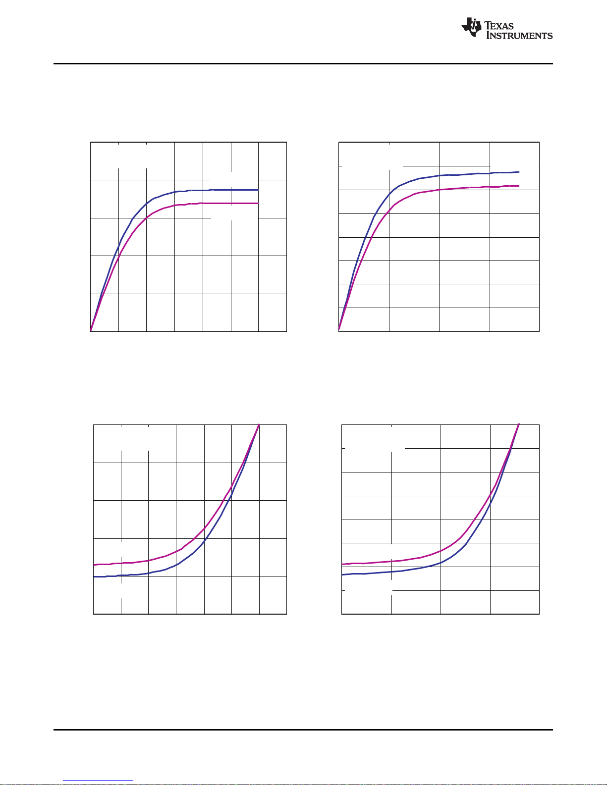
-25
-20
-15
-10
-5
0
0 0.5 1 1.5 2 2.5 3 3.5
VOH- High-Le vel Output V oltage - V
I
OH
- Typical High-Level Output Current - mA
VCC= 3.0 V
VCC= 3.0 V
P4.3
TA= 25°C
TA= 85°C
-8
-7
-6
-5
-4
-3
-2
-1
0
0 0.5 1 1.5 2
VOH- High-Le vel Output V oltage - V
I
OH
- Typical High-Level Output Current - mA
VDD= 5.5 VVDD= 5.5 V
VCC= 1.8 V
P4.3
TA= 25°C
TA= 85°C
0
5
10
15
20
25
0 0.5 1 1.5 2 2.5 3 3.5
VOL- Low -Leve l Output Voltage - V
I
OL
- Typical Low -Level Output Current - mA
VCC= 3.0 V
P4.3
TA= 25°C
TA= 85°C
0
1
2
3
4
5
6
7
8
0 0.5 1 1.5 2
VOL- Low -Leve l Output Voltage - V
I
OL
- Typical Low -Level Output Current - mA
VDD= 5.5 V
VCC= 1.8 V
P4.3
TA= 25°C
TA= 85°C
ECCN 5E002 TSPA - Technology / Software Publicly Available
CC430F6137, CC430F6135, CC430F6127, CC430F6126, CC430F6125
CC430F5137, CC430F5135, CC430F5133
SLAS554H –MAY 2009–REVISED SEPTEMBER 2013
Typical Characteristics - Outputs, Reduced Drive Strength (PxDS.y = 0)
www.ti.com
TYPICAL LOW-LEVEL OUTPUT CURRENT TYPICAL LOW-LEVEL OUTPUT CURRENT
LOW-LEVEL OUTPUT VOLTAGE LOW-LEVEL OUTPUT VOLTAGE
vs vs
Figure 6. Figure 7.
TYPICAL HIGH-LEVEL OUTPUT CURRENT TYPICAL HIGH-LEVEL OUTPUT CURRENT
HIGH-LEVEL OUTPUT VOLTAGE HIGH-LEVEL OUTPUT VOLTAGE
vs vs
Typical Characteristics - Outputs, Full Drive Strength (PxDS.y = 1)
48 Submit Documentation Feedback Copyright © 2009–2013, Texas Instruments Incorporated
Product Folder Links: CC430F6137 CC430F6135 CC430F6127 CC430F6126 CC430F6125 CC430F5137
Figure 8. Figure 9.
CC430F5135 CC430F5133
Page 49

-60
-50
-40
-30
-20
-10
0
0 0.5 1 1.5 2 2.5 3 3.5
VOH- High-Le vel Output V oltage - V
I
OH
- Typical High-Level Output Current - mA
VCC= 3.0 V
VCC= 3.0 V
P4.3
TA= 25°C
TA= 85°C
-25
-20
-15
-10
-5
0
0 0.5 1 1.5 2
VOH- High-Le vel Output V oltage - V
I
OH
- Typical High-Level Output Current - mA
VDD= 5.5 VVDD= 5.5 V
VCC= 1.8 V
P4.3
TA= 25°C
TA= 85°C
0
10
20
30
40
50
60
0 0.5 1 1.5 2 2.5 3 3.5
VOL- Low -Leve l Output Voltage - V
I
OL
- Typical Low -Level Output Current - mA
VCC= 3.0 V
P4.3
TA= 25°C
TA= 85°C
0
5
10
15
20
25
0 0.5 1 1.5 2
VOL- Low -Leve l Output Voltage - V
I
OL
- Typical Low -Level Output Current - mA
VDD= 5.5 V
VCC= 1.8 V
P4.3
TA= 25°C
TA= 85°C
www.ti.com
ECCN 5E002 TSPA - Technology / Software Publicly Available
CC430F6137, CC430F6135, CC430F6127, CC430F6126, CC430F6125
CC430F5137, CC430F5135, CC430F5133
SLAS554H –MAY 2009–REVISED SEPTEMBER 2013
TYPICAL LOW-LEVEL OUTPUT CURRENT TYPICAL LOW-LEVEL OUTPUT CURRENT
LOW-LEVEL OUTPUT VOLTAGE LOW-LEVEL OUTPUT VOLTAGE
vs vs
Figure 10. Figure 11.
TYPICAL HIGH-LEVEL OUTPUT CURRENT TYPICAL HIGH-LEVEL OUTPUT CURRENT
HIGH-LEVEL OUTPUT VOLTAGE HIGH-LEVEL OUTPUT VOLTAGE
vs vs
Copyright © 2009–2013, Texas Instruments Incorporated Submit Documentation Feedback 49
Product Folder Links: CC430F6137 CC430F6135 CC430F6127 CC430F6126 CC430F6125 CC430F5137
Figure 12. Figure 13.
CC430F5135 CC430F5133
Page 50
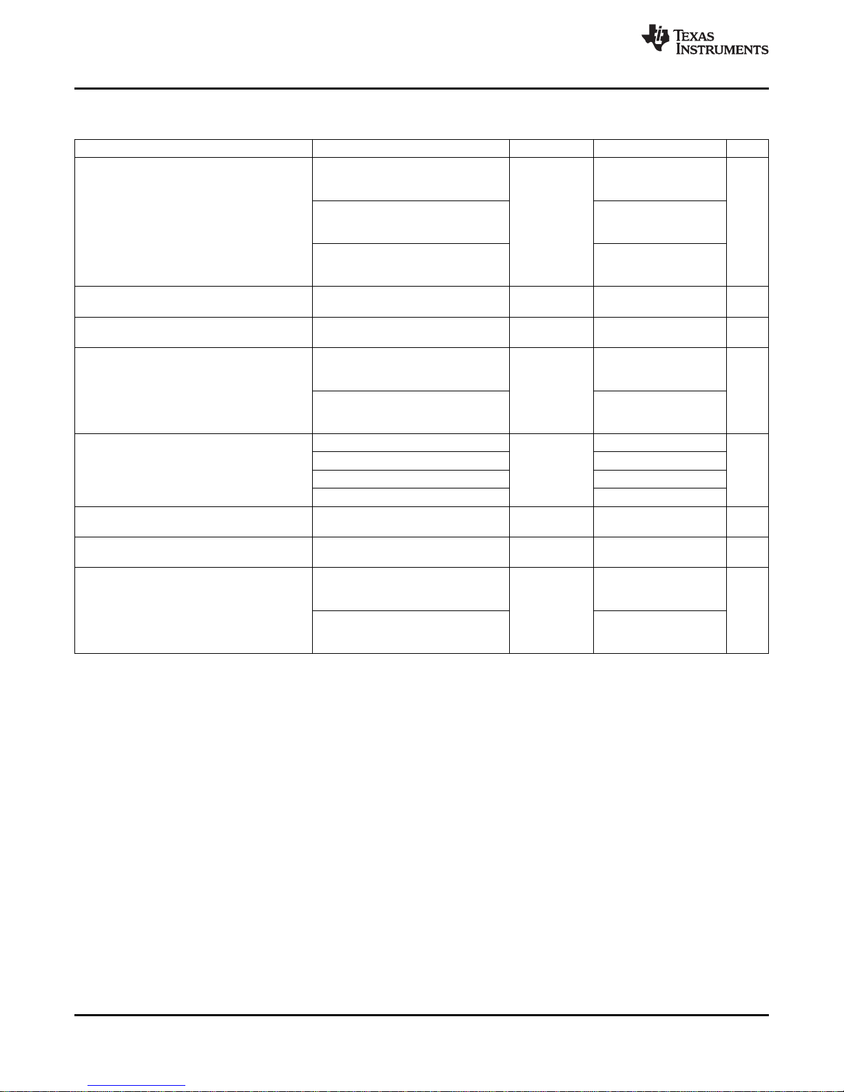
ECCN 5E002 TSPA - Technology / Software Publicly Available
CC430F6137, CC430F6135, CC430F6127, CC430F6126, CC430F6125
CC430F5137, CC430F5135, CC430F5133
SLAS554H –MAY 2009–REVISED SEPTEMBER 2013
Crystal Oscillator, XT1, Low-Frequency Mode
(1)
over recommended ranges of supply voltage and operating free-air temperature (unless otherwise noted)
PARAMETER TEST CONDITIONS V
f
= 32768 Hz, XTS = 0,
OSC
XT1BYPASS = 0, XT1DRIVEx = 1, 0.075
CC
TA= 25°C
ΔI
DVCC.LF
Differential XT1 oscillator crystal f
current consumption from lowest XT1BYPASS = 0, XT1DRIVEx = 2, 3.0 V 0.170 µA
drive setting, LF mode TA= 25°C
= 32768 Hz, XTS = 0,
OSC
f
= 32768 Hz, XTS = 0,
OSC
XT1BYPASS = 0, XT1DRIVEx = 3, 0.290
TA= 25°C
f
XT1,LF0
f
XT1,LF,SW
XT1 oscillator crystal frequency,
LF mode
XT1 oscillator logic-level squarewave input frequency, LF mode
XTS = 0, XT1BYPASS = 0 32768 Hz
XTS = 0, XT1BYPASS = 1
(2) (3)
XTS = 0,
XT1BYPASS = 0, XT1DRIVEx = 0, 210
OA
= 32768 Hz, C
LF
Oscillation allowance for
LF crystals
(4)
XT1,LF
XTS = 0,
L,eff
= 6 pF
f
XT1BYPASS = 0, XT1DRIVEx = 1, 300
f
= 32768 Hz, C
XT1,LF
XTS = 0, XCAPx = 0
C
L,eff
Integrated effective load
capacitance, LF mode
(5)
XTS = 0, XCAPx = 1 5.5
XTS = 0, XCAPx = 2 8.5
L,eff
(6)
= 12 pF
XTS = 0, XCAPx = 3 12.0
XTS = 0, Measured at ACLK,
f
= 32768 Hz
XT1,LF
XTS = 0
f
XT1BYPASS = 0, XT1DRIVEx = 0, 1000
TA= 25°C, C
f
XT1BYPASS = 0, XT1DRIVEx = 3, 500
TA= 25°C, C
(8)
= 32768 Hz, XTS = 0,
OSC
L,eff
= 32768 Hz, XTS = 0,
OSC
L,eff
= 6 pF
= 12 pF
f
Fault,LF
t
START,LF
Duty cycle, LF mode 30 70 %
Oscillator fault frequency,
LF mode
(7)
Startup time, LF mode 3.0 V ms
(1) To improve EMI on the XT1 oscillator, the following guidelines should be observed.
(a) Keep the trace between the device and the crystal as short as possible.
(b) Design a good ground plane around the oscillator pins.
(c) Prevent crosstalk from other clock or data lines into oscillator pins XIN and XOUT.
(d) Avoid running PCB traces underneath or adjacent to the XIN and XOUT pins.
(e) Use assembly materials and techniques that avoid any parasitic load on the oscillator XIN and XOUT pins.
(f) If conformal coating is used, make sure that it does not induce capacitive or resistive leakage between the oscillator pins.
(2) When XT1BYPASS is set, XT1 circuits are automatically powered down. Input signal is a digital square wave with parametrics defined in
the Schmitt-trigger Inputs section of this datasheet.
(3) Maximum frequency of operation of the entire device cannot be exceeded.
(4) Oscillation allowance is based on a safety factor of 5 for recommended crystals. The oscillation allowance is a function of the
XT1DRIVEx settings and the effective load. In general, comparable oscillator allowance can be achieved based on the following
guidelines, but should be evaluated based on the actual crystal selected for the application:
(a) For XT1DRIVEx = 0, C
(b) For XT1DRIVEx = 1, 6 pF ≤ C
(c) For XT1DRIVEx = 2, 6 pF ≤ C
(d) For XT1DRIVEx = 3, C
(5) Includes parasitic bond and package capacitance (approximately 2 pF per pin).
L,eff
L,eff
≤ 6 pF
L,eff
L,eff
≥ 6 pF
≤ 9 pF
≤ 10 pF
Because the PCB adds additional capacitance, it is recommended to verify the correct load by measuring the ACLK frequency. For a
correct setup, the effective load capacitance should always match the specification of the used crystal.
(6) Requires external capacitors at both terminals. Values are specified by crystal manufacturers.
(7) Frequencies below the MIN specification set the fault flag. Frequencies above the MAX specification do not set the fault flag.
Frequencies between the MIN and MAX specifications might set the flag
(8) Measured with logic-level input frequency but also applies to operation with crystals.
MIN TYP MAX UNIT
10 32.768 50 kHz
10 10000 Hz
www.ti.com
kΩ
2
pF
50 Submit Documentation Feedback Copyright © 2009–2013, Texas Instruments Incorporated
Product Folder Links: CC430F6137 CC430F6135 CC430F6127 CC430F6126 CC430F6125 CC430F5137
CC430F5135 CC430F5133
Page 51

ECCN 5E002 TSPA - Technology / Software Publicly Available
CC430F6137, CC430F6135, CC430F6127, CC430F6126, CC430F6125
CC430F5137, CC430F5135, CC430F5133
www.ti.com
Internal Very-Low-Power Low-Frequency Oscillator (VLO)
over recommended ranges of supply voltage and operating free-air temperature (unless otherwise noted)
PARAMETER TEST CONDITIONS V
f
VLO
df
VLO/dT
df
VLO
(1) Calculated using the box method: (MAX(-40 to 85°C) – MIN(-40 to 85°C)) / MIN(-40 to 85°C) / (85°C – (–40°C))
(2) Calculated using the box method: (MAX(1.8 to 3.6 V) – MIN(1.8 to 3.6 V)) / MIN(1.8 to 3.6 V) / (3.6 V – 1.8 V)
VLO frequency Measured at ACLK 1.8 V to 3.6 V 6 9.4 14 kHz
VLO frequency temperature drift Measured at ACLK
/dVCCVLO frequency supply voltage drift Measured at ACLK
(1)
(2)
Duty cycle Measured at ACLK 1.8 V to 3.6 V 40 50 60 %
Internal Reference, Low-Frequency Oscillator (REFO)
over recommended ranges of supply voltage and operating free-air temperature (unless otherwise noted)
PARAMETER TEST CONDITIONS V
I
REFO
f
REFO
df
REFO/dT
df
/dV
REFO
t
START
(1) Calculated using the box method: (MAX(-40 to 85°C) – MIN(-40 to 85°C)) / MIN(-40 to 85°C) / (85°C – (–40°C))
(2) Calculated using the box method: (MAX(1.8 to 3.6 V) – MIN(1.8 to 3.6 V)) / MIN(1.8 to 3.6 V) / (3.6 V – 1.8 V)
REFO oscillator current consumption TA= 25°C 1.8 V to 3.6 V 3 µA
REFO frequency calibrated Measured at ACLK 1.8 V to 3.6 V 32768 Hz
REFO absolute tolerance calibrated %
REFO frequency temperature drift Measured at ACLK
REFO frequency supply voltage drift Measured at ACLK
CC
Full temperature range 1.8 V to 3.6 V ±3.5
TA= 25°C 3 V ±1.5
(1)
(2)
Duty cycle Measured at ACLK 1.8 V to 3.6 V 40 50 60 %
REFO startup time 40%/60% duty cycle 1.8 V to 3.6 V 25 µs
SLAS554H –MAY 2009–REVISED SEPTEMBER 2013
CC
MIN TYP MAX UNIT
1.8 V to 3.6 V 0.5 %/°C
1.8 V to 3.6 V 4 %/V
CC
MIN TYP MAX UNIT
1.8 V to 3.6 V 0.01 %/°C
1.8 V to 3.6 V 1.0 %/V
Copyright © 2009–2013, Texas Instruments Incorporated Submit Documentation Feedback 51
Product Folder Links: CC430F6137 CC430F6135 CC430F6127 CC430F6126 CC430F6125 CC430F5137
CC430F5135 CC430F5133
Page 52

0
1 2
3
4
5
6
7
Typical DCO Frequency, V = 3.0 V, T = 25°C
CC A
DCORSEL
100
10
1
0.1
f – MHz
DCO
DCOx = 31
DCOx = 0
ECCN 5E002 TSPA - Technology / Software Publicly Available
CC430F6137, CC430F6135, CC430F6127, CC430F6126, CC430F6125
CC430F5137, CC430F5135, CC430F5133
SLAS554H –MAY 2009–REVISED SEPTEMBER 2013
DCO Frequency
over recommended ranges of supply voltage and operating free-air temperature (unless otherwise noted)
PARAMETER TEST CONDITIONS MIN TYP MAX UNIT
f
DCO(0,0)
f
DCO(0,31)
f
DCO(1,0)
f
DCO(1,31)
f
DCO(2,0)
f
DCO(2,31)
f
DCO(3,0)
f
DCO(3,31)
f
DCO(4,0)
f
DCO(4,31)
f
DCO(5,0)
f
DCO(5,31)
f
DCO(6,0)
f
DCO(6,31)
f
DCO(7,0)
f
DCO(7,31)
S
DCORSEL
S
DCO
DCO frequency (0, 0)
DCO frequency (0, 31)
DCO frequency (1, 0)
DCO frequency (1, 31)
DCO frequency (2, 0)
DCO frequency (2, 31)
DCO frequency (3, 0)
DCO frequency (3, 31)
DCO frequency (4, 0)
DCO frequency (4, 31)
DCO frequency (5, 0)
DCO frequency (5, 31)
DCO frequency (6, 0)
DCO frequency (6, 31)
DCO frequency (7, 0)
DCO frequency (7, 31)
Frequency step between range
DCORSEL and DCORSEL + 1
Frequency step between tap
DCO and DCO + 1
Duty cycle Measured at SMCLK 40 50 60 %
df
/dT DCO frequency temperature drift f
DCO
df
DCO
/dV
CC
DCO frequency voltage drift f
(1) When selecting the proper DCO frequency range (DCORSELx), the target DCO frequency, f
range of f
range n, tap 0 (DCOx = 0) and f
DCO(n, 0),MAX
≤ f
DCO
(DCOx = 31). This ensures that the target DCO frequency resides within the range selected. It should also be noted that if the actual
f
frequency for the selected range causes the FLL or the application to select tap 0 or 31, the DCO fault flag is set to report that the
DCO
selected range is at its minimum or maximum tap setting.
(1)
(1)
(1)
(1)
(1)
(1)
(1)
(1)
≤ f
DCO(n, 31),MIN
DCO(n,31),MIN
DCORSELx = 0, DCOx = 0, MODx = 0 0.07 0.20 MHz
(1)
DCORSELx = 0, DCOx = 31, MODx = 0 0.70 1.70 MHz
DCORSELx = 1, DCOx = 0, MODx = 0 0.15 0.36 MHz
(1)
DCORSELx = 1, DCOx = 31, MODx = 0 1.47 3.45 MHz
DCORSELx = 2, DCOx = 0, MODx = 0 0.32 0.75 MHz
(1)
DCORSELx = 2, DCOx = 31, MODx = 0 3.17 7.38 MHz
DCORSELx = 3, DCOx = 0, MODx = 0 0.64 1.51 MHz
(1)
DCORSELx = 3, DCOx = 31, MODx = 0 6.07 14.0 MHz
DCORSELx = 4, DCOx = 0, MODx = 0 1.3 3.2 MHz
(1)
DCORSELx = 4, DCOx = 31, MODx = 0 12.3 28.2 MHz
DCORSELx = 5, DCOx = 0, MODx = 0 2.5 6.0 MHz
(1)
DCORSELx = 5, DCOx = 31, MODx = 0 23.7 54.1 MHz
DCORSELx = 6, DCOx = 0, MODx = 0 4.6 10.7 MHz
(1)
DCORSELx = 6, DCOx = 31, MODx = 0 39.0 88.0 MHz
DCORSELx = 7, DCOx = 0, MODx = 0 8.5 19.6 MHz
(1)
DCORSELx = 7, DCOx = 31, MODx = 0 60 135 MHz
S
= f
RSEL
DCO(DCORSEL+1,DCO)/fDCO(DCORSEL,DCO)
S
= f
DCO
DCO(DCORSEL,DCO+1)/fDCO(DCORSEL,DCO)
= 1 MHz 0.1 %/°C
DCO
= 1 MHz 1.9 %/V
DCO
, should be set to reside within the
, where f
DCO(n, 0),MAX
represents the minimum frequency specified for the DCO frequency, range n, tap 31
represents the maximum frequency specified for the DCO frequency,
DCO
1.2 2.3 ratio
1.02 1.12 ratio
www.ti.com
52 Submit Documentation Feedback Copyright © 2009–2013, Texas Instruments Incorporated
Product Folder Links: CC430F6137 CC430F6135 CC430F6127 CC430F6126 CC430F6125 CC430F5137
Figure 14. Typical DCO frequency
CC430F5135 CC430F5133
Page 53
ECCN 5E002 TSPA - Technology / Software Publicly Available
CC430F6137, CC430F6135, CC430F6127, CC430F6126, CC430F6125
CC430F5137, CC430F5135, CC430F5133
www.ti.com
PMM, Brown-Out Reset (BOR)
over recommended ranges of supply voltage and operating free-air temperature (unless otherwise noted)
PARAMETER TEST CONDITIONS MIN TYP MAX UNIT
V(DVCC_BOR_IT–) BORHon voltage, DVCCfalling level | dDVCC/dt| < 3 V/s 1.45 V
V(DVCC_BOR_IT+) BORHoff voltage, DVCCrising level | dDVCC/dt| < 3 V/s 0.80 1.30 1.50 V
V(DVCC_BOR_hys) BORHhysteresis 60 250 mV
t
RESET
Pulse duration required at RST/NMI pin to accept a reset 2 µs
PMM, Core Voltage
over recommended ranges of supply voltage and operating free-air temperature (unless otherwise noted)
PARAMETER TEST CONDITIONS MIN TYP MAX UNIT
V
(AM) Core voltage, active mode, PMMCOREV = 3 2.4 V ≤ DVCC≤ 3.6 V 1.90 V
CORE3
V
(AM) Core voltage, active mode, PMMCOREV = 2 2.2 V ≤ DVCC≤ 3.6 V 1.80 V
CORE2
V
(AM) Core voltage, active mode, PMMCOREV = 1 2.0 V ≤ DVCC≤ 3.6 V 1.60 V
CORE1
V
(AM) Core voltage, active mode, PMMCOREV = 0 1.8 V ≤ DVCC≤ 3.6 V 1.40 V
CORE0
V
(LPM) Core voltage, low-current mode, PMMCOREV = 3 2.4 V ≤ DVCC≤ 3.6 V 1.94 V
CORE3
V
(LPM) Core voltage, low-current mode, PMMCOREV = 2 2.2 V ≤ DVCC≤ 3.6 V 1.84 V
CORE2
V
(LPM) Core voltage, low-current mode, PMMCOREV = 1 2.0 V ≤ DVCC≤ 3.6 V 1.64 V
CORE1
V
(LPM) Core voltage, low-current mode, PMMCOREV = 0 1.8 V ≤ DVCC≤ 3.6 V 1.44 V
CORE0
SLAS554H –MAY 2009–REVISED SEPTEMBER 2013
PMM, SVS High Side
over recommended ranges of supply voltage and operating free-air temperature (unless otherwise noted)
PARAMETER TEST CONDITIONS MIN TYP MAX UNIT
SVSHE = 0, DVCC= 3.6 V 0
I
(SVSH)
SVS current consumption SVSHE = 1, DVCC= 3.6 V, SVSHFP = 0 200
SVSHE = 1, DVCC= 3.6 V, SVSHFP = 1 1.5 µA
SVSHE = 1, SVSHRVL = 0 1.53 1.60 1.67
V
(SVSH_IT–)
SVSHon voltage level
(1)
SVSHE = 1, SVSHRVL = 1 1.73 1.80 1.87
SVSHE = 1, SVSHRVL = 2 1.93 2.00 2.07
SVSHE = 1, SVSHRVL = 3 2.03 2.10 2.17
SVSHE = 1, SVSMHRRL = 0 1.60 1.70 1.80
SVSHE = 1, SVSMHRRL = 1 1.80 1.90 2.00
SVSHE = 1, SVSMHRRL = 2 2.00 2.10 2.20
V
(SVSH_IT+)
SVSHoff voltage level
(1)
SVSHE = 1, SVSMHRRL = 3 2.10 2.20 2.30
SVSHE = 1, SVSMHRRL = 4 2.25 2.35 2.50
SVSHE = 1, SVSMHRRL = 5 2.52 2.65 2.78
SVSHE = 1, SVSMHRRL = 6 2.85 3.00 3.15
SVSHE = 1, SVSMHRRL = 7 2.85 3.00 3.15
t
pd(SVSH)
t
(SVSH)
dV
DVCC
SVSHpropagation delay µs
SVSHon or off delay time µs
/dt DVCCrise time 0 1000 V/s
SVSHE = 1, dV
SVSHE = 1, dV
SVSHE = 0 → 1, dV
SVSHE = 0 → 1, dV
/dt = 10 mV/µs, SVSHFP = 1 2.5
DVCC
/dt = 1 mV/µs, SVSHFP = 0 20
DVCC
/dt = 10 mV/µs, SVSHFP = 1 12.5
DVCC
/dt = 1 mV/µs, SVSHFP = 0 100
DVCC
(1) The SVSHsettings available depend on the VCORE (PMMCOREVx) setting. See the Power Management Module and Supply Voltage
Supervisor chapter in the CC430 Family User's Guide (SLAU259) on recommended settings and usage.
nA
V
V
Copyright © 2009–2013, Texas Instruments Incorporated Submit Documentation Feedback 53
Product Folder Links: CC430F6137 CC430F6135 CC430F6127 CC430F6126 CC430F6125 CC430F5137
CC430F5135 CC430F5133
Page 54

ECCN 5E002 TSPA - Technology / Software Publicly Available
CC430F6137, CC430F6135, CC430F6127, CC430F6126, CC430F6125
CC430F5137, CC430F5135, CC430F5133
SLAS554H –MAY 2009–REVISED SEPTEMBER 2013
PMM, SVM High Side
over recommended ranges of supply voltage and operating free-air temperature (unless otherwise noted)
PARAMETER TEST CONDITIONS MIN TYP MAX UNIT
SVMHE = 0, DVCC= 3.6 V 0
I
(SVMH)
V
(SVMH)
t
pd(SVMH)
t
(SVMH)
(1) The SVMHsettings available depend on the VCORE (PMMCOREVx) setting. See the Power Management Module and Supply Voltage
Supervisor chapter in the CC430 Family User's Guide (SLAU259) on recommended settings and usage.
SVMHcurrent consumption SVMHE= 1, DVCC= 3.6 V, SVMHFP = 0 200
SVMHE = 1, DVCC= 3.6 V, SVMHFP = 1 1.5 µA
SVMHE = 1, SVSMHRRL = 0 1.60 1.70 1.80
SVMHE = 1, SVSMHRRL = 1 1.80 1.90 2.00
SVMHE = 1, SVSMHRRL = 2 2.00 2.10 2.20
SVMHE = 1, SVSMHRRL = 3 2.10 2.20 2.30
SVMHon or off voltage level
(1)
SVMHE = 1, SVSMHRRL = 4 2.25 2.35 2.50 V
SVMHE = 1, SVSMHRRL = 5 2.52 2.65 2.78
SVMHE = 1, SVSMHRRL = 6 2.85 3.00 3.15
SVMHE = 1, SVSMHRRL = 7 2.85 3.00 3.15
SVMHE = 1, SVMHOVPE = 1 3.75
SVMHE = 1, dV
SVMHpropagation delay µs
SVMHFP = 1
SVMHE = 1, dV
SVMHFP = 0
SVMHE = 0 → 1, dV
SVMHon or off delay time µs
SVMHFP = 1
SVMHE = 0 → 1, dV
SVMHFP = 0
/dt = 10 mV/µs,
DVCC
/dt = 1 mV/µs,
DVCC
DVCC
DVCC
/dt = 10 mV/µs,
/dt = 1 mV/µs,
2.5
20
12.5
100
www.ti.com
nA
54 Submit Documentation Feedback Copyright © 2009–2013, Texas Instruments Incorporated
Product Folder Links: CC430F6137 CC430F6135 CC430F6127 CC430F6126 CC430F6125 CC430F5137
CC430F5135 CC430F5133
Page 55
ECCN 5E002 TSPA - Technology / Software Publicly Available
CC430F6137, CC430F6135, CC430F6127, CC430F6126, CC430F6125
CC430F5137, CC430F5135, CC430F5133
www.ti.com
PMM, SVS Low Side
over recommended ranges of supply voltage and operating free-air temperature (unless otherwise noted)
PARAMETER TEST CONDITIONS MIN TYP MAX UNIT
SVSLE = 0, PMMCOREV = 2 0 nA
I
(SVSL)
t
pd(SVSL)
t
(SVSL)
SVSLcurrent consumption SVSLE = 1, PMMCOREV = 2, SVSLFP = 0 200 nA
SVSLE = 1, PMMCOREV = 2, SVSLFP = 1 1.5 µA
SVSLE = 1, dV
SVSLpropagation delay µs
SVSLFP = 1
SVSLE = 1, dV
SVSLFP = 0
SVSLE = 0 → 1, dV
SVSLon or off delay time µs
SVSLFP = 1
SVSLE = 0 → 1, dV
SVSLFP = 0
/dt = 10 mV/µs,
CORE
/dt = 1 mV/µs,
CORE
CORE
CORE
/dt = 10 mV/µs,
/dt = 1 mV/µs,
PMM, SVM Low Side
over recommended ranges of supply voltage and operating free-air temperature (unless otherwise noted)
PARAMETER TEST CONDITIONS MIN TYP MAX UNIT
SVMLE = 0, PMMCOREV = 2 0 nA
I
(SVML)
t
pd(SVML)
t
(SVML)
SVMLcurrent consumption SVMLE= 1, PMMCOREV = 2, SVMLFP = 0 200 nA
SVMLE= 1, PMMCOREV = 2, SVMLFP = 1 1.5 µA
SVMLE = 1, dV
SVMLpropagation delay µs
SVMLFP = 1
SVMLE = 1, dV
SVMLFP = 0
SVMLE = 0 → 1, dV
SVMLon or off delay time µs
SVMLFP = 1
SVMLE = 0 → 1, dV
SVMLFP = 0
/dt = 10 mV/µs,
CORE
/dt = 1 mV/µs,
CORE
CORE
CORE
/dt = 10 mV/µs,
/dt = 1 mV/µs,
SLAS554H –MAY 2009–REVISED SEPTEMBER 2013
2.5
20
12.5
100
2.5
20
12.5
100
Wake Up From Low Power Modes and Reset
over recommended ranges of supply voltage and operating free-air temperature (unless otherwise noted)
PARAMETER TEST CONDITIONS MIN TYP MAX UNIT
t
WAKE-UP-FAST
t
WAKE-UP-SLOW
t
WAKE-UP-RESET
Wake-up time from LPM2, LPM3, or
LPM4 to active mode
Wake-up time from LPM2, LPM3 or
LPM4 to active mode
Wake-up time from RST or BOR
event to active mode
(1)
(2)
(3)
PMMCOREV = SVSMLRRL = n f
(where n = 0, 1, 2, or 3), µs
SVSLFP = 1
PMMCOREV = SVSMLRRL = n
(where n = 0, 1, 2, or 3), 150 165 µs
SVSLFP = 0
(1) This value represents the time from the wake-up event to the first active edge of MCLK. The wake-up time depends on the performance
mode of the low-side supervisor (SVSL) and low side monitor (SVML). Fastest wake-up times are possible with SVSLand SVMLin full
performance mode or disabled when operating in AM, LPM0, and LPM1. Various options are available for SVSLand SVMLwhile
operating in LPM2, LPM3, and LPM4. See the Power Management Module and Supply Voltage Supervisor chapter in the CC430 Family
User's Guide (SLAU259).
(2) This value represents the time from the wake-up event to the first active edge of MCLK. The wake-up time depends on the performance
mode of the low-side supervisor (SVSL) and low side monitor (SVML). In this case, the SVSLand SVMLare in normal mode (low current)
mode when operating in AM, LPM0, and LPM1. Various options are available for SVSLand SVMLwhile operating in LPM2, LPM3, and
LPM4. See the Power Management Module and Supply Voltage Supervisor chapter in the CC430 Family User's Guide (SLAU259).
(3) This value represents the time from the wake-up event to the reset vector execution.
≥ 4.0 MHz 5
MCLK
f
< 4.0 MHz 6
MCLK
2 3 ms
Copyright © 2009–2013, Texas Instruments Incorporated Submit Documentation Feedback 55
Product Folder Links: CC430F6137 CC430F6135 CC430F6127 CC430F6126 CC430F6125 CC430F5137
CC430F5135 CC430F5133
Page 56

ECCN 5E002 TSPA - Technology / Software Publicly Available
CC430F6137, CC430F6135, CC430F6127, CC430F6126, CC430F6125
CC430F5137, CC430F5135, CC430F5133
SLAS554H –MAY 2009–REVISED SEPTEMBER 2013
Timer_A
over recommended ranges of supply voltage and operating free-air temperature (unless otherwise noted)
f
TA
t
TA,cap
PARAMETER TEST CONDITIONS V
Internal: SMCLK, ACLK,
Timer_A input clock frequency External: TACLK, 1.8 V, 3 V 25 MHz
Duty cycle = 50% ± 10%
All capture inputs,
Timer_A capture timing Minimum pulse duration required for 1.8 V, 3 V 20 ns
capture.
CC
MIN TYP MAX UNIT
www.ti.com
56 Submit Documentation Feedback Copyright © 2009–2013, Texas Instruments Incorporated
Product Folder Links: CC430F6137 CC430F6135 CC430F6127 CC430F6126 CC430F6125 CC430F5137
CC430F5135 CC430F5133
Page 57

ECCN 5E002 TSPA - Technology / Software Publicly Available
CC430F6137, CC430F6135, CC430F6127, CC430F6126, CC430F6125
CC430F5137, CC430F5135, CC430F5133
www.ti.com
USCI (UART Mode) Recommended Operating Conditions
PARAMETER CONDITIONS V
Internal: SMCLK, ACLK,
f
USCI
f
BITCLK
USCI input clock frequency External: UCLK, f
Duty cycle = 50% ± 10%
BITCLK clock frequency
(equals baud rate in MBaud)
USCI (UART Mode)
over recommended ranges of supply voltage and operating free-air temperature (unless otherwise noted)
PARAMETER TEST CONDITIONS V
t
τ
UART receive deglitch time
(1) Pulses on the UART receive input (UCxRX) shorter than the UART receive deglitch time are suppressed. To ensure that pulses are
correctly recognized, their duration should exceed the maximum specification of the deglitch time.
(1)
USCI (SPI Master Mode) Recommended Operating Conditions
PARAMETER CONDITIONS V
f
USCI
USCI input clock frequency f
Internal: SMCLK, ACLK
Duty cycle = 50% ± 10%
SLAS554H –MAY 2009–REVISED SEPTEMBER 2013
CC
MIN TYP MAX UNIT
SYSTEM
1 MHz
CC
MIN TYP MAX UNIT
2.2 V 50 600
3 V 50 600
CC
MIN TYP MAX UNIT
SYSTEM
MHz
ns
MHz
USCI (SPI Master Mode)
over recommended ranges of supply voltage and operating free-air temperature (unless otherwise noted)
(see Note
t
SU,MI
t
HD,MI
t
VALID,MO
t
HD,MO
(1) f
(2) Specifies the time to drive the next valid data to the SIMO output after the output changing UCLK clock edge. See the timing diagrams
(3) Specifies how long data on the SIMO output is valid after the output changing UCLK clock edge. Negative values indicate that the data
(1)
, Figure 15 and Figure 16)
PARAMETER TEST CONDITIONS PMMCOREVx V
SOMI input data setup time
SOMI input data hold time
SIMO output data valid time
SIMO output data hold time
= 1/2t
UCxCLK
For the slave's parameters t
LO/HI
with t
LO/HI
≥ max(t
SU,SI(Slave)
UCLK edge to SIMO valid,
(2)
CL= 20 pF
(3)
CL= 20 pF
VALID,MO(USCI)
and t
+ t
VALID,SO(Slave)
SU,SI(Slave)
CC
0 ns
3 ns
0 ns
3 ns
0 ns
3 ns
0 ns
3 ns
, t
SU,MI(USCI)
see the SPI parameters of the attached slave.
+ t
VALID,SO(Slave)
1.8 V 55
3.0 V 38
2.4 V 30
3.0 V 25
1.8 V 0
3.0 V 0
2.4 V 0
3.0 V 0
1.8 V 20
3.0 V 18
2.4 V 16
3.0 V 15
1.8 V -10
3.0 V -8
2.4 V -10
3.0 V -8
).
MIN TYP MAX UNIT
in Figure 15 and Figure 16.
on the SIMO output can become invalid before the output changing clock edge observed on UCLK. See the timing diagrams in
Figure 15 and Figure 16.
Copyright © 2009–2013, Texas Instruments Incorporated Submit Documentation Feedback 57
Product Folder Links: CC430F6137 CC430F6135 CC430F6127 CC430F6126 CC430F6125 CC430F5137
CC430F5135 CC430F5133
Page 58
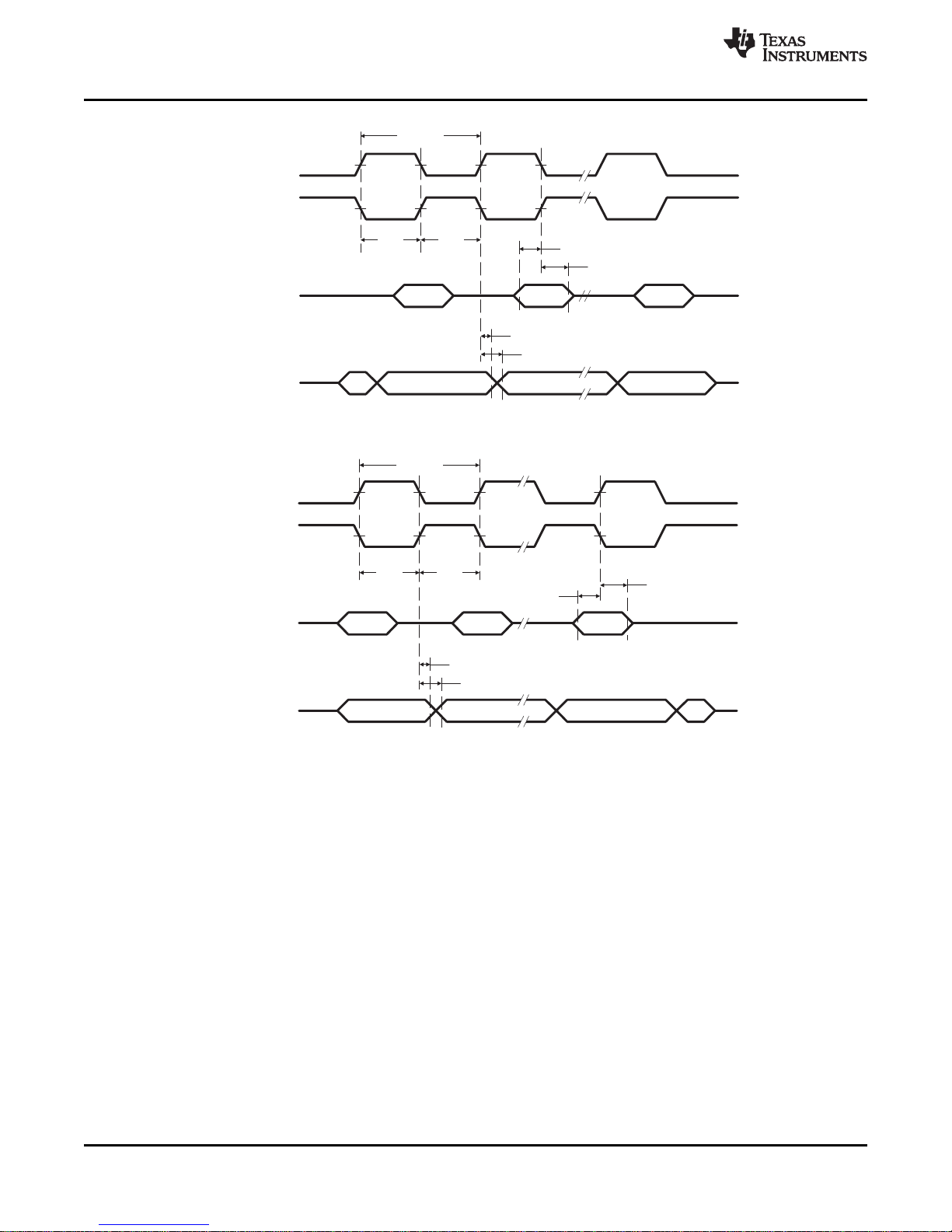
t
SU,MI
t
HD,MI
UCLK
SOMI
SIMO
t
VALID,MO
CKPL =0
CKPL =1
1/f
UCxCLK
t
HD,MO
t
LO/HI
t
LO/HI
t
SU,MI
t
HD,MI
UCLK
SOMI
SIMO
t
VALID,MO
t
HD,MO
CKPL =0
CKPL =1
t
LO/HI
t
LO/HI
1/f
UCxCLK
ECCN 5E002 TSPA - Technology / Software Publicly Available
CC430F6137, CC430F6135, CC430F6127, CC430F6126, CC430F6125
CC430F5137, CC430F5135, CC430F5133
SLAS554H –MAY 2009–REVISED SEPTEMBER 2013
Figure 15. SPI Master Mode, CKPH = 0
www.ti.com
58 Submit Documentation Feedback Copyright © 2009–2013, Texas Instruments Incorporated
Product Folder Links: CC430F6137 CC430F6135 CC430F6127 CC430F6126 CC430F6125 CC430F5137
Figure 16. SPI Master Mode, CKPH = 1
CC430F5135 CC430F5133
Page 59
ECCN 5E002 TSPA - Technology / Software Publicly Available
CC430F6137, CC430F6135, CC430F6127, CC430F6126, CC430F6125
CC430F5137, CC430F5135, CC430F5133
www.ti.com
USCI (SPI Slave Mode)
over recommended ranges of supply voltage and operating free-air temperature (unless otherwise noted)
(see Note
t
STE,LEAD
t
STE,LAG
t
STE,ACC
t
STE,DIS
t
SU,SI
t
HD,SI
t
VALID,SO
t
HD,SO
(1) f
(2) Specifies the time to drive the next valid data to the SOMI output after the output changing UCLK clock edge. See the timing diagrams
(3) Specifies how long data on the SOMI output is valid after the output changing UCLK clock edge. See the timing diagrams in Figure 15
(1)
, Figure 17 and Figure 18)
PARAMETER TEST CONDITIONS PMMCOREVx V
STE lead time, STE low to clock
STE lag time, Last clock to STE
high
STE access time, STE low to
SOMI data out
STE disable time, STE high to
SOMI high impedance
SIMO input data setup time
SIMO input data hold time
SOMI output data valid time
SOMI output data hold time
= 1/2t
UCxCLK
For the master's parameters t
LO/HI
with t
LO/HI
in Figure 15 and Figure 16.
and Figure 16.
(2)
(3)
≥ max(t
VALID,MO(Master)
SU,MI(Master)
UCLK edge to SOMI valid,
CL= 20 pF
CL= 20 pF
and t
VALID,MO(Master)
+ t
SU,SI(USCI)
, t
see the SPI parameters of the attached master.
SU,MI(Master)
+ t
SLAS554H –MAY 2009–REVISED SEPTEMBER 2013
CC
0 ns
3
0 ns
3
0 ns
3
0 ns
3
0 ns
3 ns
0 ns
3 ns
0 ns
3 ns
0 ns
3 ns
VALID,SO(USCI)
1.8 V 11
3.0 V 8
2.4 V 7
3.0 V 6
1.8 V 3
3.0 V 3
2.4 V 3
3.0 V 3
1.8 V 66
3.0 V 50
2.4 V 36
3.0 V 30
1.8 V 30
3.0 V 23
2.4 V 16
3.0 V 13
1.8 V 5
3.0 V 5
2.4 V 2
3.0 V 2
1.8 V 5
3.0 V 5
2.4 V 5
3.0 V 5
1.8 V 76
3.0 V 60
2.4 V 44
3.0 V 40
1.8 V 18
3.0 V 12
2.4 V 10
3.0 V 8
).
MIN TYP MAX UNIT
Copyright © 2009–2013, Texas Instruments Incorporated Submit Documentation Feedback 59
Product Folder Links: CC430F6137 CC430F6135 CC430F6127 CC430F6126 CC430F6125 CC430F5137
CC430F5135 CC430F5133
Page 60

STE
UCLK
CKPL =0
CKPL =1
SOMI
SIMO
t
SU,SI
t
HD,SI
t
VALID,SO
t
STE,LEAD
1/f
UCxCLK
t
STE,LAG
t
STE,DIS
t
STE,ACC
t
HD,MO
t
LO/HI
t
LO/HI
STE
UCLK
CKPL =0
CKPL =1
SOMI
SIMO
t
SU,SI
t
HD,SI
t
VALID,SO
t
STE,LEAD
1/f
UCxCLK
t
LO/HI
t
LO/HI
t
STE,LAG
t
STE,DIS
t
STE,ACC
t
HD,SO
ECCN 5E002 TSPA - Technology / Software Publicly Available
CC430F6137, CC430F6135, CC430F6127, CC430F6126, CC430F6125
CC430F5137, CC430F5135, CC430F5133
SLAS554H –MAY 2009–REVISED SEPTEMBER 2013
www.ti.com
Figure 17. SPI Slave Mode, CKPH = 0
Figure 18. SPI Slave Mode, CKPH = 1
60 Submit Documentation Feedback Copyright © 2009–2013, Texas Instruments Incorporated
Product Folder Links: CC430F6137 CC430F6135 CC430F6127 CC430F6126 CC430F6125 CC430F5137
CC430F5135 CC430F5133
Page 61

SDA
SCL
t
HD,DAT
t
SU,DAT
t
HD,STA
t
HIGH
t
LOW
t
BUF
t
HD,STA
t
SU,STA
t
SP
t
SU,STO
ECCN 5E002 TSPA - Technology / Software Publicly Available
CC430F6137, CC430F6135, CC430F6127, CC430F6126, CC430F6125
CC430F5137, CC430F5135, CC430F5133
www.ti.com
USCI (I2C Mode)
over recommended ranges of supply voltage and operating free-air temperature (unless otherwise noted) (see Figure 19)
PARAMETER TEST CONDITIONS V
f
USCI
f
SCL
t
HD,STA
t
SU,STA
t
HD,DAT
t
SU,DAT
t
SU,STO
t
SP
USCI input clock frequency External: UCLK f
SCL clock frequency 2.2 V, 3 V 0 400 kHz
Hold time (repeated) START 2.2 V, 3 V µs
Setup time for a repeated START 2.2 V, 3 V µs
Data hold time 2.2 V, 3 V 0 ns
Data setup time 2.2 V, 3 V 250 ns
Setup time for STOP 2.2 V, 3 V µs
Pulse duration of spikes suppressed by input filter ns
Internal: SMCLK, ACLK
Duty cycle = 50% ± 10%
f
≤ 100 kHz 4.0
SCL
f
> 100 kHz 0.6
SCL
f
≤ 100 kHz 4.7
SCL
f
> 100 kHz 0.6
SCL
f
≤ 100 kHz 4.0
SCL
f
> 100 kHz 0.6
SCL
SLAS554H –MAY 2009–REVISED SEPTEMBER 2013
CC
MIN TYP MAX UNIT
SYSTEM
2.2 V 50 600
3 V 50 600
MHz
Figure 19. I2C Mode Timing
Copyright © 2009–2013, Texas Instruments Incorporated Submit Documentation Feedback 61
Product Folder Links: CC430F6137 CC430F6135 CC430F6127 CC430F6126 CC430F6125 CC430F5137
CC430F5135 CC430F5133
Page 62

ECCN 5E002 TSPA - Technology / Software Publicly Available
CC430F6137, CC430F6135, CC430F6127, CC430F6126, CC430F6125
CC430F5137, CC430F5135, CC430F5133
SLAS554H –MAY 2009–REVISED SEPTEMBER 2013
LCD_B Recommended Operating Conditions
PARAMETER CONDITIONS MIN NOM MAX UNIT
V
CC,LCD_B,CP en,3.6
V
CC,LCD_B,CP en,3.3
V
CC,LCD_B,int. bias
V
CC,LCD_B,ext. bias
V
CC,LCD_B,VLCDEXT
V
LCDCAP/R33
C
LCDCAP
f
Frame
f
ACLK,in
C
Panel
V
R33
V
R23,1/3bias
V
R13,1/3bias
V
R13,1/2bias
V
R03
V
LCD-VR03
V
LCDREF/R13
Supply voltage range, charge LCDCPEN = 1, 0000 < VLCDx ≤ 1111
pump enabled, V
≤ 3.6 V (charge pump enabled, V
LCD
LCD
≤ 3.6 V)
Supply voltage range, charge LCDCPEN = 1, 0000 < VLCDx ≤ 1100
pump enabled, V
Supply voltage range, internal
biasing, charge pump disabled
Supply voltage range, external
biasing, charge pump disabled
≤ 3.3 V (charge pump enabled, V
LCD
LCDCPEN = 0, VLCDEXT=0 2.4 3.6 V
LCDCPEN = 0, VLCDEXT=0 2.4 3.6 V
LCD
≤ 3.3 V)
Supply voltage range, external
LCD voltage, internal or
external biasing, charge pump
LCDCPEN = 0, VLCDEXT=1 2.0 3.6 V
disabled
External LCD voltage at
LCDCAP/R33, internal or
external biasing, charge pump
LCDCPEN = 0, VLCDEXT=1 2.4 3.6 V
disabled
Capacitor on LCDCAP when LCDCPEN = 1, VLCDx > 0000 (charge
charge pump enabled pump enabled)
f
= 2 × mux × f
LCD frame frequency range 0 100 Hz
LCD
mux = 1 (static), 2, 3, 4
FRAME
with
ACLK input frequency range 30 32 40 kHz
Panel capacitance 100-Hz frame frequency 10000 pF
Analog input voltage at R33 LCDCPEN = 0, VLCDEXT=1 2.4 VCC+0.2 V
Analog input voltage at R23 V
LCDREXT = 1, LCDEXTBIAS = 1,
LCD2B = 0
Analog input voltage at R13 LCDREXT = 1, LCDEXTBIAS = 1,
with 1/3 biasing LCD2B = 0
Analog input voltage at R13 LCDREXT = 1, LCDEXTBIAS = 1,
with 1/2 biasing LCD2B = 1
Analog input voltage at R03 R0EXT=1 V
Voltage difference between
V
and R03
LCD
LCDCPEN = 0, R0EXT=1 2.4 VCC+0.2 V
External LCD reference
voltage applied at VLCDREFx = 01 0.8 1.2 1.5 V
LCDREF/R13
www.ti.com
2.2 3.6 V
2.0 3.6 V
4.7 4.7 10 µF
V
+
R03
2/3*(V
R13
V
R03
V
R03
SS
-V
V
1/3*(V
-V
V
1/2*(V
-V
R33
R03
R03
R33
R03
R03
R33
R03
V
)
R33
+
V
)
R23
+
V
)
R33
V
V
V
V
62 Submit Documentation Feedback Copyright © 2009–2013, Texas Instruments Incorporated
Product Folder Links: CC430F6137 CC430F6135 CC430F6127 CC430F6126 CC430F6125 CC430F5137
CC430F5135 CC430F5133
Page 63

ECCN 5E002 TSPA - Technology / Software Publicly Available
CC430F6137, CC430F6135, CC430F6127, CC430F6126, CC430F6125
www.ti.com
LCD_B Electrical Characteristics
over operating free-air temperature range (unless otherwise noted)
PARAMETER TEST CONDITIONS V
V
LCD
I
CC,Peak,CP
t
LCD,CP,on
I
CP,Load
R
LCD,Seg
R
LCD,COM
LCD voltage VLCDx = 0000, VLCDEXT = 0 2.4 V to 3.6 V V
LCDCPEN = 1, VLCDx = 0001 2.0 V to 3.6 V 2.54 V
LCDCPEN = 1, VLCDx = 0010 2.0 V to 3.6 V 2.60 V
LCDCPEN = 1, VLCDx = 0011 2.0 V to 3.6 V 2.66 V
LCDCPEN = 1, VLCDx = 0100 2.0 V to 3.6 V 2.72 V
LCDCPEN = 1, VLCDx = 0101 2.0 V to 3.6 V 2.78 V
LCDCPEN = 1, VLCDx = 0110 2.0 V to 3.6 V 2.84 V
LCDCPEN = 1, VLCDx = 0111 2.0 V to 3.6 V 2.90 V
LCDCPEN = 1, VLCDx = 1000 2.0 V to 3.6 V 2.96 V
LCDCPEN = 1, VLCDx = 1001 2.0 V to 3.6 V 3.02 V
LCDCPEN = 1, VLCDx = 1010 2.0 V to 3.6 V 3.08 V
LCDCPEN = 1, VLCDx = 1011 2.0 V to 3.6 V 3.14 V
LCDCPEN = 1, VLCDx = 1100 2.0 V to 3.6 V 3.20 V
LCDCPEN = 1, VLCDx = 1101 2.2 V to 3.6 V 3.26 V
LCDCPEN = 1, VLCDx = 1110 2.2 V to 3.6 V 3.32 V
LCDCPEN = 1, VLCDx = 1111 2.2 V to 3.6 V 3.38 3.6 V
Peak supply currents due to LCDCPEN = 1, VLCDx = 1111 2.2 V 200 µA
charge pump activities
Time to charge C
discharged LCDCPEN = 0→1,
when C
LCD
= 4.7µF, 2.2 V 100 500 ms
LCDCAP
VLCDx = 1111
Maximum charge pump load LCDCPEN = 1, VLCDx = 1111 2.2 V 50 µA
current
LCD driver output LCDCPEN = 1, VLCDx = 1000, 2.2 V 10 kΩ
impedance, segment lines I
LOAD
= ±10 µA
LCD driver output LCDCPEN = 1, VLCDx = 1000, 2.2 V 10 kΩ
impedance, common lines I
LOAD
= ±10 µA
CC430F5137, CC430F5135, CC430F5133
SLAS554H –MAY 2009–REVISED SEPTEMBER 2013
CC
MIN TYP MAX UNIT
CC
V
Copyright © 2009–2013, Texas Instruments Incorporated Submit Documentation Feedback 63
Product Folder Links: CC430F6137 CC430F6135 CC430F6127 CC430F6126 CC430F6125 CC430F5137
CC430F5135 CC430F5133
Page 64
ECCN 5E002 TSPA - Technology / Software Publicly Available
CC430F6137, CC430F6135, CC430F6127, CC430F6126, CC430F6125
CC430F5137, CC430F5135, CC430F5133
SLAS554H –MAY 2009–REVISED SEPTEMBER 2013
12-Bit ADC, Power Supply and Input Range Conditions
over recommended ranges of supply voltage and operating free-air temperature (unless otherwise noted)
PARAMETER TEST CONDITIONS V
AV
CC
V
(Ax)
I
ADC12_A
C
I
R
I
Analog supply voltage,
Full performance
Analog input voltage range
Operating supply current into
AVCC terminal
(3)
Input capacitance 2.2 V 20 25 pF
Input MUX ON resistance 0 V ≤ VAx≤ AV
AVCC and DVCC are connected together,
AVSS and DVSS are connected together, 2.2 3.6 V
V
= V
(AVSS)
(2)
All ADC12 analog input pins Ax 0 AV
f
ADC12CLK
REFON = 0, SHT0 = 0, SHT1 = 0, µA
= 0 V
(DVSS)
= 5.0 MHz, ADC12ON = 1, 2.2 V 125 155
ADC12DIV = 0
Only one terminal Ax can be selected at one
time
CC
(1) The leakage current is specified by the digital I/O input leakage.
(2) The analog input voltage range must be within the selected reference voltage range VR+to VR–for valid conversion results. If the
reference voltage is supplied by an external source or if the internal reference voltage is used and REFOUT = 1, then decoupling
capacitors are required. See REF, External Reference and REF, Built-In Reference.
(3) The internal reference supply current is not included in current consumption parameter I
CC
3 V 150 220
.
ADC12_A
(1)
MIN TYP MAX UNIT
10 200 1900 Ω
12-Bit ADC, Timing Parameters
over recommended ranges of supply voltage and operating free-air temperature (unless otherwise noted)
PARAMETER TEST CONDITIONS V
CC
For specified performance of ADC12 linearity
f
ADC12CLK
f
ADC12OSC
t
CONVERT
t
Sample
parameters using an external reference voltage or 0.45 4.8 5.0
AVCC as reference.
ADC conversion clock For specified performance of ADC12 linearity 2.2 V, 3 V MHz
parameters using the internal reference.
For specified performance of ADC12 linearity
parameters using the internal reference.
Internal ADC12
oscillator
(4)
ADC12DIV = 0, f
REFON = 0, Internal oscillator,
f
Conversion time µs
ADC12OSC
External f
ADC12SSEL ≠ 0
Sampling time 2.2 V, 3 V 1000 ns
RS= 400 Ω, RI= 1000 Ω, CI= 30 pF,
τ = [RS+ RI] × C
= 4.2 MHz to 5.4 MHz
ADC12CLK
(1)
(2)
(3)
ADC12CLK
= f
ADC12OSC
from ACLK, MCLK or SMCLK,
(6)
I
2.2 V, 3 V 4.2 4.8 5.4 MHz
2.2 V, 3 V 2.4 3.1
(1) REFOUT = 0, external reference voltage: SREF2 = 0, SREF1 = 1, SREF0 = 0. AVCC as reference voltage: SREF2 = 0, SREF1 = 0,
SREF0 = 0. The specified performance of the ADC12 linearity is ensured when using the ADC12OSC. For other clock sources, the
specified performance of the ADC12 linearity is ensured with f
(2) SREF2 = 0, SREF1 = 1, SREF0 = 0, ADC12SR = 0, REFOUT = 1
ADC12CLK
maximum of 5.0 MHz.
(3) SREF2 = 0, SREF1 = 1, SREF0 = 0, ADC12SR = 0, REFOUT = 0. The specified performance of the ADC12 linearity is ensured when
using the ADC12OSC divided by 2.
(4) The ADC12OSC is sourced directly from MODOSC inside the UCS.
(5) 13 × ADC12DIV × 1/f
(6) Approximately ten Tau (τ) are needed to get an error of less than ±0.5 LSB:
t
Sample
= ln(2
n+1
ADC12CLK
) x (RS+ RI) × CI+ 800 ns, where n = ADC resolution = 12, RS= external source resistance
MIN TYP MAX UNIT
0.45 2.4 4.0
0.45 2.4 2.7
(5)
www.ti.com
V
CC
64 Submit Documentation Feedback Copyright © 2009–2013, Texas Instruments Incorporated
Product Folder Links: CC430F6137 CC430F6135 CC430F6127 CC430F6126 CC430F6125 CC430F5137
CC430F5135 CC430F5133
Page 65

ECCN 5E002 TSPA - Technology / Software Publicly Available
CC430F6137, CC430F6135, CC430F6127, CC430F6126, CC430F6125
CC430F5137, CC430F5135, CC430F5133
www.ti.com
12-Bit ADC, Linearity Parameters Using an External Reference Voltage or AVCC as Reference
Voltage
over recommended ranges of supply voltage and operating free-air temperature (unless otherwise noted)
PARAMETER TEST CONDITIONS V
E
E
E
E
E
Integral linearity error
I
Differential linearity error
D
Offset error
O
Gain error
G
Total unadjusted error LSB
T
(3)
(3) (2)
(1)
(1) (2)
1.4 V ≤ dVREF ≤ 1.6 V
1.6 V < dVREF
dVREF ≤ 2.2 V
dVREF > 2.2 V
dVREF ≤ 2.2 V
dVREF > 2.2 V
(1) Parameters are derived using the histogram method.
(2) The external reference voltage is selected by: SREF2 = 0 or 1, SREF1 = 1, SREF0 = 0. dVREF = VR+- VR-, VR+< AVCC, VR-> AVSS.
Unless otherwise mentioned, dVREF > 1.5 V. Impedance of the external reference voltage R < 100 Ω and two decoupling capacitors,
10 µF and 100 nF, should be connected to VREF+/VREF- to decouple the dynamic current. See also the CC430 Family User's Guide
(SLAU259).
(3) Parameters are derived using a best fit curve.
(2)
(2)
(2)
(2)
(2)
(2)
SLAS554H –MAY 2009–REVISED SEPTEMBER 2013
CC
2.2 V, 3 V LSB
MIN TYP MAX UNIT
±2.0
±1.7
2.2 V, 3 V ±1.0 LSB
2.2 V, 3 V ±1.0 ±2.0
2.2 V, 3 V ±1.0 ±2.0
LSB
2.2 V, 3 V ±1.0 ±2.0 LSB
2.2 V, 3 V ±1.4 ±3.5
2.2 V, 3 V ±1.4 ±3.5
12-Bit ADC, Linearity Parameters Using the Internal Reference Voltage
over recommended ranges of supply voltage and operating free-air temperature (unless otherwise noted)
PARAMETER TEST CONDITIONS
I
Integral linearity
(2)
error
E
ADC12SR = 0, REFOUT = 1 f
ADC12SR = 0, REFOUT = 0 f
ADC12SR = 0, REFOUT = 1 f
D
Differential
linearity error
ADC12SR = 0, REFOUT = 1 f
(2)
E
ADC12SR = 0, REFOUT = 0 f
ADC12SR = 0, REFOUT = 1 f
E
E
E
O
G
T
Offset error
Gain error
Total unadjusted
error
(3)
ADC12SR = 0, REFOUT = 0 f
ADC12SR = 0, REFOUT = 1 f
(3)
ADC12SR = 0, REFOUT = 0 f
ADC12SR = 0, REFOUT = 1 f
ADC12SR = 0, REFOUT = 0 f
(1) The internal reference voltage is selected by: SREF2 = 0 or 1, SREF1 = 1, SREF0 = 1. dVREF = VR+- VR-.
(2) Parameters are derived using the histogram method.
(3) Parameters are derived using a best fit curve.
(4) The gain error and total unadjusted error are dominated by the accuracy of the integrated reference module absolute accuracy. In this
mode the reference voltage used by the ADC12_A is not available on a pin.
(1)
ADC12CLK
ADC12CLK
ADC12CLK
ADC12CLK
ADC12CLK
ADC12CLK
ADC12CLK
ADC12CLK
ADC12CLK
ADC12CLK
ADC12CLK
V
CC
≤ 4.0 MHz ±1.7
≤ 2.7 MHz ±2.5
2.2 V, 3 V LSB
MIN TYP MAX UNIT
≤ 4.0 MHz -1.0 +2.0
≤ 2.7 MHz 2.2 V, 3 V -1.0 +1.5 LSB
≤ 2.7 MHz -1.0 +2.5
≤ 4.0 MHz ±1.0 ±2.0
≤ 2.7 MHz ±1.0 ±2.0
≤ 4.0 MHz ±1.0 ±2.0 LSB
≤ 2.7 MHz ±1.5%
≤ 4.0 MHz ±1.4 ±3.5 LSB
≤ 2.7 MHz ±1.5%
2.2 V, 3 V LSB
2.2 V, 3 V
2.2 V, 3 V
(4)
VREF
(4)
VREF
Copyright © 2009–2013, Texas Instruments Incorporated Submit Documentation Feedback 65
Product Folder Links: CC430F6137 CC430F6135 CC430F6127 CC430F6126 CC430F6125 CC430F5137
CC430F5135 CC430F5133
Page 66
500
550
600
650
700
750
800
850
900
950
1000
-40 -30 -20 -10 0 10 20 30 40 50 60 70 80
Typical Temperature Sensor Voltage
- mV
Ambient Temperature - ˚C
ECCN 5E002 TSPA - Technology / Software Publicly Available
CC430F6137, CC430F6135, CC430F6127, CC430F6126, CC430F6125
CC430F5137, CC430F5135, CC430F5133
SLAS554H –MAY 2009–REVISED SEPTEMBER 2013
12-Bit ADC, Temperature Sensor and Built-In V
MID
(1)
over recommended ranges of supply voltage and operating free-air temperature (unless otherwise noted)
PARAMETER TEST CONDITIONS V
V
SENSOR
TC
SENSOR
t
SENSOR(sample)
V
MID
(2) (3)
See
(3)
See
Sample time required if ADC12ON = 1, INCH = 0Ah,
channel 10 is selected
(4)
AVCCdivider at channel 11,
V
factor
AVCC
ADC12ON = 1, INCH = 0Ah,
TA= 0°C
ADC12ON = 1, INCH = 0Ah mV/°C
Error of conversion result ≤ 1 LSB
ADC12ON = 1, INCH = 0Bh 0.48 0.5 0.52 V
AVCCdivider at channel 11 ADC12ON = 1, INCH = 0Bh V
t
VMID(sample)
Sample time required if ADC12ON = 1, INCH = 0Bh,
channel 11 is selected
(5)
Error of conversion result ≤ 1 LSB
(1) The temperature sensor is provided by the REF module. See the REF module parametric, I
the temperature sensor.
CC
2.2 V 680
3 V 680
2.2 V 2.25
3 V 2.25
2.2 V 30
3 V 30
2.2 V 1.06 1.1 1.14
3 V 1.44 1.5 1.56
2.2 V, 3 V 1000 ns
, regarding the current consumption of
REF+
(2) The temperature sensor offset can be as much as ±20°C. A single-point calibration is recommended to minimize the offset error of the
built-in temperature sensor.
(3) The device descriptor structure contains calibration values for 30°C ± 3°C and 85°C ± 3°C for each of the available reference voltage
levels. The sensor voltage can be computed as V
be computed from the calibration values for higher accuracy.
SENSE
= TC
* (Temperature, °C) + V
SENSOR
SENSOR
(4) The typical equivalent impedance of the sensor is 51 kΩ. The sample time required includes the sensor-on time t
(5) The on-time t
is included in the sampling time t
VMID(on)
VMID(sample)
; no additional on time is needed.
MIN TYP MAX UNIT
, where TC
SENSOR
SENSOR(on)
and V
www.ti.com
mV
µs
AVCC
SENSOR
.
can
Figure 20. Typical Temperature Sensor Voltage
66 Submit Documentation Feedback Copyright © 2009–2013, Texas Instruments Incorporated
Product Folder Links: CC430F6137 CC430F6135 CC430F6127 CC430F6126 CC430F6125 CC430F5137
CC430F5135 CC430F5133
Page 67
ECCN 5E002 TSPA - Technology / Software Publicly Available
CC430F6137, CC430F6135, CC430F6127, CC430F6126, CC430F6125
CC430F5137, CC430F5135, CC430F5133
www.ti.com
REF, External Reference
over recommended ranges of supply voltage and operating free-air temperature (unless otherwise noted)
PARAMETER TEST CONDITIONS V
V
eREF+
V
REF–/VeREF–
(V
– Differential external reference voltage
eREF+
V
REF–/VeREF–
I
VeREF+
I
VREF–/VeREF–
C
VREF+/-
(1) The external reference is used during ADC conversion to charge and discharge the capacitance array. The input capacitance, Ci, is also
the dynamic load for an external reference during conversion. The dynamic impedance of the reference supply should follow the
recommendations on analog-source impedance to allow the charge to settle for 12-bit accuracy.
(2) The accuracy limits the minimum positive external reference voltage. Lower reference voltage levels may be applied with reduced
accuracy requirements.
(3) The accuracy limits the maximum negative external reference voltage. Higher reference voltage levels may be applied with reduced
accuracy requirements.
(4) The accuracy limits minimum external differential reference voltage. Lower differential reference voltage levels may be applied with
reduced accuracy requirements.
(5) Two decoupling capacitors, 10 µF and 100 nF, should be connected to VREF to decouple the dynamic current required for an external
reference source if it is used for the ADC12_A. See also the CC430 Family User's Guide (SLAU259).
Positive external reference voltage input V
Negative external reference voltage input V
) input
Static input current
Capacitance at VREF+ or VREF- terminal,
external reference
(5)
> V
eREF+
eREF+
V
eREF+
1.4 V ≤ V
V
eREF–
f
ADC12CLK
MHz,ADC12SHTx = 1h,
REF–/VeREF–
> V
REF–/VeREF–
> V
REF–/VeREF–
≤ V
eREF+
= 0 V
AVCC
= 5 2.2 V, 3 V ±8.5 ±26 µA
Conversion rate 200ksps
1.4 V ≤ V
V
eREF–
f
ADC12CLK
MHz,ADC12SHTx = 8h,
≤ V
eREF+
= 0 V
AVCC
= 5 2.2 V, 3 V ±1 µA
Conversion rate 20ksps
SLAS554H –MAY 2009–REVISED SEPTEMBER 2013
(1)
(2)
CC
(3)
(4)
MIN TYP MAX UNIT
1.4 AV
0 1.2 V
1.4 AV
,
,
10 µF
CC
CC
V
V
Copyright © 2009–2013, Texas Instruments Incorporated Submit Documentation Feedback 67
Product Folder Links: CC430F6137 CC430F6135 CC430F6127 CC430F6126 CC430F6125 CC430F5137
CC430F5135 CC430F5133
Page 68

ECCN 5E002 TSPA - Technology / Software Publicly Available
CC430F6137, CC430F6135, CC430F6127, CC430F6126, CC430F6125
CC430F5137, CC430F5135, CC430F5133
SLAS554H –MAY 2009–REVISED SEPTEMBER 2013
REF, Built-In Reference
over recommended ranges of supply voltage and operating free-air temperature (unless otherwise noted)
PARAMETER TEST CONDITIONS V
REFVSEL = 2 for 2.5 V,
REFON = REFOUT = 1, 3 V 2.41 ±1.5%
I
= 0 A
VREF+
V
REF+
Positive built-in reference
voltage output
REFVSEL = 1 for 2.0 V,
REFON = REFOUT = 1, 3 V 1.93 ±1.5% V
I
= 0 A
VREF+
REFVSEL = 0 for 1.5 V,
REFON = REFOUT = 1, 2.2 V, 3 V 1.45 ±1.5%
I
= 0 A
VREF+
REFVSEL = 0 for 1.5 V, reduced performance 1.8
AV
CC(min)
AVCC minimum voltage,
Positive built-in reference V
active
REFVSEL = 0 for 1.5 V 2.2
REFVSEL = 1 for 2.0 V 2.3
REFVSEL = 2 for 2.5 V 2.8
I
REF+
Operating supply current into
AVCC terminal
(2)(3)
REFON = 1, REFOUT = 0, REFBURST = 0 3 V 100 140 µA
REFON = 1, REFOUT = 1, REFBURST = 0 3 V 0.9 1.5 mA
REFVSEL = 0, 1, or 2,
I
L(VREF+)
C
VREF+
TC
REF+
PSRR_DC TA= 25 °C, REFVSEL = 0, 1, or 2, 120 300 µV/V
PSRR_AC 6.4 mV/V
Load-current regulation, I
VREF+ terminal
(4)
Capacitance at VREF+
terminals, internal reference
Temperature coefficient of ppm/
built-in reference
(5)
Power supply rejection ratio
(dc)
Power supply rejection ratio TA= 25 °C, f = 1 kHz, ΔVpp = 100 mV,
(ac) REFVSEL = 0, 1, or 2,
= +10 µA or –1000 µA,
VREF+
AVCC= AV
REFON = REFOUT = 1
for each reference level,
CC (min)
REFON = REFOUT = 1 20 100 pF
I
= 0 A,
VREF+
REFVSEL = 0, 1, or 2, 30 50
REFON = 1, REFOUT = 0 or 1
AVCC= AV
CC (min)
- AV
CC(max)
,
REFON = 1, REFOUT = 0 or 1
AVCC= AV
CC (min)
- AV
CC(max)
REFON = 1, REFOUT = 0 or 1
t
SETTLE
Settling time of reference
(6)
voltage
AVCC= AV
REFVSEL = 0, 1, or 2, 75
REFOUT = 0, REFON = 0 → 1
AVCC= AV
C
= C
VREF
REFVSEL = 0, 1, or 2,
CC (min)
CC (min)
VREF
- AV
- AV
(max),
CC(max)
CC(max)
,
,
REFOUT = 1, REFON = 0 → 1
(1) The reference is supplied to the ADC by the REF module and is buffered locally inside the ADC. The ADC uses two internal buffers, one
smaller and one larger for driving the VREF+ terminal. When REFOUT = 1, the reference is available at the VREF+ terminal, as well as,
used as the reference for the conversion and utilizes the larger buffer. When REFOUT = 0, the reference is only used as the reference
for the conversion and utilizes the smaller buffer.
(2) The internal reference current is supplied from the AVCC terminal. Consumption is independent of the ADC12ON control bit, unless a
conversion is active. The REFON bit enables to settle the built-in reference before starting an A/D conversion. REFOUT = 0 represents
the current contribution of the smaller buffer. REFOUT = 1 represents the current contribution of the larger buffer without external load.
(3) The temperature sensor is provided by the REF module. Its current is supplied from the AVCC terminal and is equivalent to I
REFON =1 and REFOUT = 0.
(4) Contribution only due to the reference and buffer including package. This does not include resistance due to PCB trace or other causes.
(5) Calculated using the box method: (MAX(-40 to 85°C) – MIN(-40 to 85°C)) / MIN(-40 to 85°C)/(85°C – (–40°C)).
(6) The condition is that the error in a conversion started after t
capacitive load when REFOUT = 1.
is less than ±0.5 LSB. The settling time depends on the external
REFON
CC
(1)
MIN TYP MAX UNIT
75
www.ti.com
2500 µV/mA
°C
µs
with
REF+
68 Submit Documentation Feedback Copyright © 2009–2013, Texas Instruments Incorporated
Product Folder Links: CC430F6137 CC430F6135 CC430F6127 CC430F6126 CC430F6125 CC430F5137
CC430F5135 CC430F5133
Page 69

ECCN 5E002 TSPA - Technology / Software Publicly Available
CC430F6137, CC430F6135, CC430F6127, CC430F6126, CC430F6125
CC430F5137, CC430F5135, CC430F5133
www.ti.com
Comparator_B
over recommended ranges of supply voltage and operating free-air temperature (unless otherwise noted)
PARAMETER TEST CONDITIONS V
V
CC
I
AVCC_COMP
I
AVCC_REF
V
IC
V
OFFSET
C
IN
R
SIN
t
PD
t
PD,filter
t
EN_CMP
t
EN_REF
V
CB_REF
Supply voltage 1.8 3.6 V
Comparator operating supply current
CBPWRMD = 00 2.2 V 30 50
into AVCC, Excludes reference 3.0 V 40 65 µA
resistor ladder
CBPWRMD = 01 2.2 V, 3 V 10 30
CBPWRMD = 10 2.2 V, 3 V 0.1 0.5
Quiescent current of local reference
voltage amplifier into AVCC
CBREFACC = 1, CBREFLx = 01 22 µA
Common mode input range 0 VCC-1 V
Input offset voltage
CBPWRMD = 00 ±20 mV
CBPWRMD = 01, 10 ±10 mV
Input capacitance 5 pF
Series input resistance
ON - switch closed 3 4 kΩ
OFF - switch opened 30 MΩ
CBPWRMD = 00, CBF = 0 450 ns
Propagation delay, response time CBPWRMD = 01, CBF = 0 600 ns
CBPWRMD = 10, CBF = 0 50 µs
CBPWRMD = 00, CBON = 1,
CBF = 1, CBFDLY = 00
CBPWRMD = 00, CBON = 1,
Propagation delay with filter active
CBF = 1, CBFDLY = 01
CBPWRMD = 00, CBON = 1,
CBF = 1, CBFDLY = 10
CBPWRMD = 00, CBON = 1,
CBF = 1, CBFDLY = 11
Comparator enable time, settling time 1 2 µs
CBON = 0 to CBON = 1,
CBPWRMD = 00, 01, 10
Resistor reference enable time CBON = 0 to CBON = 1 0.3 1.5 µs
Reference voltage for a given tap VIN × (n+1) / 32 V
VIN = reference into resistor ladder,
n = 0 to 31
SLAS554H –MAY 2009–REVISED SEPTEMBER 2013
CC
MIN TYP MAX UNIT
1.8 V 40
0.35 0.6 1.0 µs
0.6 1.0 1.8 µs
1.0 1.8 3.4 µs
1.8 3.4 6.5 µs
Copyright © 2009–2013, Texas Instruments Incorporated Submit Documentation Feedback 69
Product Folder Links: CC430F6137 CC430F6135 CC430F6127 CC430F6126 CC430F6125 CC430F5137
CC430F5135 CC430F5133
Page 70
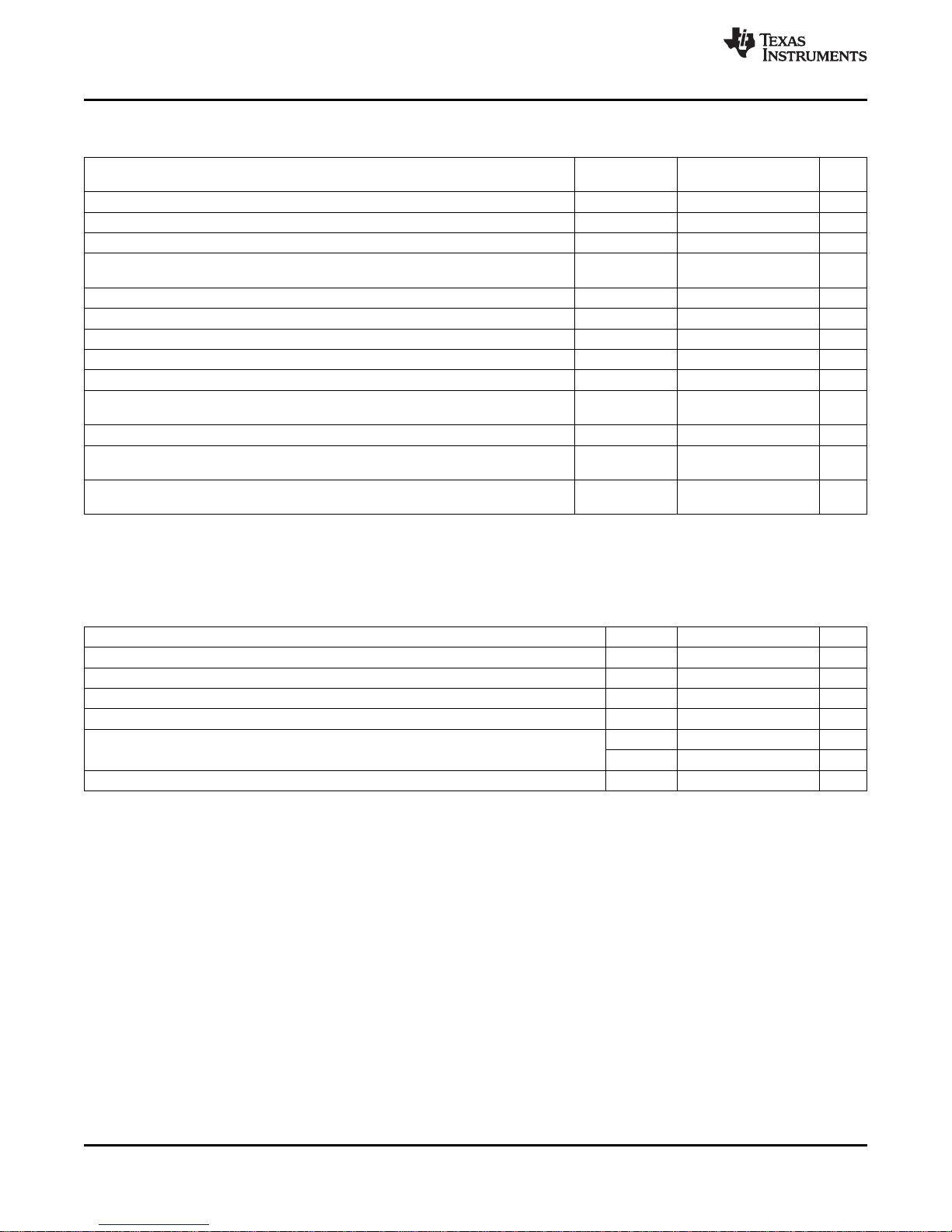
ECCN 5E002 TSPA - Technology / Software Publicly Available
CC430F6137, CC430F6135, CC430F6127, CC430F6126, CC430F6125
CC430F5137, CC430F5135, CC430F5133
SLAS554H –MAY 2009–REVISED SEPTEMBER 2013
Flash Memory
over recommended ranges of supply voltage and operating free-air temperature (unless otherwise noted)
PARAMETER MIN TYP MAX UNIT
DV
CC(PGM/ERASE)
I
PGM
I
ERASE
I
, I
MERASE
t
CPT
BANK
Program and erase supply voltage 1.8 3.6 V
Average supply current from DVCC during program 3 5 mA
Average supply current from DVCC during erase 2 6.5 mA
Average supply current from DVCC during mass erase or bank
erase
Cumulative program time
(1)
Program and erase endurance 10
t
Retention
t
Word
t
Block, 0
t
Block, 1–(N–1)
t
Block, N
t
Erase
f
MCLK,MGR
Data retention duration TJ= 25°C 100 years
Word or byte program time
Block program time for first byte or word
Block program time for each additional byte or word, except for last
byte or word
(2)
Block program time for last byte or word
Erase time for segment erase, mass erase, and bank erase when
available
(2)
(2)
(2)
(2)
MCLK frequency in marginal read mode
(FCTL4.MGR0 = 1 or FCTL4. MGR1 = 1)
(1) The cumulative program time must not be exceeded when writing to a 128-byte flash block. This parameter applies to all programming
methods: individual word write, individual byte write, and block write modes.
(2) These values are hardwired into the flash controller's state machine.
TEST
CONDITIONS
4
10
64 85 µs
49 65 µs
37 49 µs
55 73 µs
23 32 ms
0 1 MHz
www.ti.com
2 6.5 mA
16 ms
5
cycles
JTAG and Spy-Bi-Wire Interface
over recommended ranges of supply voltage and operating free-air temperature (unless otherwise noted)
PARAMETER V
f
SBW
t
SBW,Low
t
SBW, En
t
SBW,Rst
f
TCK
R
internal
Spy-Bi-Wire input frequency 2.2 V, 3 V 0 20 MHz
Spy-Bi-Wire low clock pulse duration 2.2 V, 3 V 0.025 15 µs
Spy-Bi-Wire enable time (TEST high to acceptance of first clock edge)
Spy-Bi-Wire return to normal operation time 15 100 µs
TCK input frequency - 4-wire JTAG
(2)
Internal pulldown resistance on TEST 2.2 V, 3 V 45 60 80 kΩ
(1) Tools that access the Spy-Bi-Wire interface need to wait for the minimum t
applying the first SBWTCK clock edge.
(2) f
may be restricted to meet the timing requirements of the module selected.
TCK
CC
(1)
2.2 V, 3 V 1 µs
2.2 V 0 5 MHz
3 V 0 10 MHz
time after pulling the TEST/SBWTCK pin high before
SBW,En
MIN TYP MAX UNIT
70 Submit Documentation Feedback Copyright © 2009–2013, Texas Instruments Incorporated
Product Folder Links: CC430F6137 CC430F6135 CC430F6127 CC430F6126 CC430F6125 CC430F5137
CC430F5135 CC430F5133
Page 71

ECCN 5E002 TSPA - Technology / Software Publicly Available
CC430F6137, CC430F6135, CC430F6127, CC430F6126, CC430F6125
CC430F5137, CC430F5135, CC430F5133
www.ti.com
RF1A CC1101-Based Radio Parameters
Recommended Operating Conditions
PARAMETER TEST CONDITIONS MIN TYP MAX UNIT
V
CC
PMMCOREVx Core voltage range, PMMCOREVx setting during radio operation 2 3
RF frequency range 389
Data rate 2-GFSK, OOK, and ASK 0.6 250 kBaud
RF crystal frequency 26 26 27 MHz
RF crystal tolerance Total tolerance including initial tolerance, crystal loading, aging and ±40 ppm
RF crystal load capacitance 10 13 20 pF
RF crystal effective series 100 Ω
resistance
(1) If using a 27-MHz crystal, the lower frequency limit for this band is 392 MHz.
(2) If using optional Manchester encoding, the data rate in kbps is half the baud rate.
(3) The acceptable crystal tolerance depends on frequency band, channel bandwidth, and spacing. Also see design note DN005 -- CC11xx
Sensitivity versus Frequency Offset and Crystal Accuracy (SWRA122).
Supply voltage range during radio operation 2.0 3.6 V
2-FSK 0.6 500
(Shaped) MSK (also known as differential offset QPSK)
temperature dependency.
(3)
SLAS554H –MAY 2009–REVISED SEPTEMBER 2013
300 348
(1)
779 928
(2)
26 500
464 MHz
RF Crystal Oscillator, XT2
TA= 25°C, VCC= 3 V (unless otherwise noted)
PARAMETER TEST CONDITIONS MIN TYP MAX UNIT
Start-up time
Duty cycle 45 50 55 %
(1) All measurement results are obtained using the EM430F6137RF900 with BOM according to tested frequency range (see Table 48).
(2) The start-up time depends to a very large degree on the used crystal.
(2)
(1)
150 810 µs
Current Consumption, Reduced-Power Modes
TA= 25°C, VCC= 3 V (unless otherwise noted)
PARAMETER TEST CONDITIONS MIN TYP MAX UNIT
Current RF crystal oscillator only (for example, SLEEP state with MCSM0.OSC_FORCE_ON = 100 µA
consumption 1)
IDLE state (including RF crystal oscillator) 1.7 mA
FSTXON state (only the frequency synthesizer is running)
(1) All measurement results are obtained using the EM430F6137RF900 with BOM according to tested frequency range (see Table 48).
(2) This current consumption is also representative of other intermediate states when going from IDLE to RX or TX, including the calibration
state.
(1)
(2)
9.5 mA
Copyright © 2009–2013, Texas Instruments Incorporated Submit Documentation Feedback 71
Product Folder Links: CC430F6137 CC430F6135 CC430F6127 CC430F6126 CC430F6125 CC430F5137
CC430F5135 CC430F5133
Page 72

ECCN 5E002 TSPA - Technology / Software Publicly Available
CC430F6137, CC430F6135, CC430F6127, CC430F6126, CC430F6125
CC430F5137, CC430F5135, CC430F5133
SLAS554H –MAY 2009–REVISED SEPTEMBER 2013
Current Consumption, Receive Mode
TA= 25°C, VCC= 3 V (unless otherwise noted)
PARAMETER RATE TEST CONDITIONS MIN TYP MAX UNIT
Current Register settings
consumption, 433 38.4 optimized for reduced mA
RX current
(1) All measurement results are obtained using the EM430F6137RF900 with BOM according to tested frequency range (see Table 48).
(2) Reduced current setting (MDMCFG2.DEM_DCFILT_OFF = 1) gives a slightly lower current consumption at the cost of a reduction in
sensitivity. See tables "RF Receive" for additional details on current consumption and sensitivity.
(3) For 868 or 915 MHz, see Figure 21 for current consumption with register settings optimized for sensitivity.
FREQ
(MHz)
315 38.4 optimized for reduced
868, 915 38.4 optimized for reduced
DATA
(kBaud)
1.2
250
1.2
250
1.2
250
(1) (2)
Register settings
current
Register settings
(3)
current
Input at -100 dBm (close to
sensitivity limit)
Input at -40 dBm (well above
sensitivity limit)
Input at -100 dBm (close to
sensitivity limit)
Input at -40 dBm (well above
sensitivity limit)
Input at -100 dBm (close to
sensitivity limit)
Input at -40 dBm (well above
sensitivity limit)
Input at -100 dBm (close to
sensitivity limit)
Input at -40 dBm (well above
sensitivity limit)
Input at -100 dBm (close to
sensitivity limit)
Input at -40 dBm (well above
sensitivity limit)
Input at -100 dBm (close to
sensitivity limit)
Input at -40 dBm (well above
sensitivity limit)
Input at -100 dBm (close to
sensitivity limit)
Input at -40 dBm (well above
sensitivity limit)
Input at -100 dBm (close to
sensitivity limit)
Input at -40 dBm (well above
sensitivity limit)
Input at -100 dBm (close to
sensitivity limit)
Input at -40 dBm (well above
sensitivity limit)
17
16
17
16
18
16.5
18
17
18
17
18.5
17
16
15
16
15
16
15
www.ti.com
72 Submit Documentation Feedback Copyright © 2009–2013, Texas Instruments Incorporated
Product Folder Links: CC430F6137 CC430F6135 CC430F6127 CC430F6126 CC430F6125 CC430F5137
CC430F5135 CC430F5133
Page 73

16
17
18
19
-100 -80 -60 -40 -20
Input Pow e r [dBm]
Radio Current [mA]
TA= 85°C
TA= 25°C
TA= -40°C
16
17
18
19
-100 -80 -60 -40 -20
Input Pow e r [dBm]
Radio Current [mA]
TA= 85°C
TA= 25°C
TA= -40°C
16
17
18
19
-100 -80 -60 -40 -20
Input Pow e r [dBm]
Radio Current [mA]
TA= 85°C
TA= 25°C
TA= -40°C
16
17
18
19
-100 -80 -60 -40 -20
Input Pow e r [dBm]
Radio Current [mA]
TA= 85°C
TA= 25°C
TA= -40°C
1.2 kBaud GFSK
250 kBaud GFSK
38.4 kBaud GFSK
500 kBaud MSK
www.ti.com
ECCN 5E002 TSPA - Technology / Software Publicly Available
CC430F6137, CC430F6135, CC430F6127, CC430F6126, CC430F6125
CC430F5137, CC430F5135, CC430F5133
SLAS554H –MAY 2009–REVISED SEPTEMBER 2013
Figure 21. Typical RX Current Consumption Over Temperature and Input Power Level, 868 MHz,
Copyright © 2009–2013, Texas Instruments Incorporated Submit Documentation Feedback 73
Product Folder Links: CC430F6137 CC430F6135 CC430F6127 CC430F6126 CC430F6125 CC430F5137
Sensitivity-Optimized Setting
CC430F5135 CC430F5133
Page 74
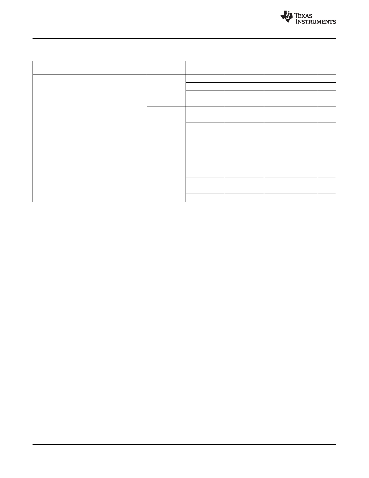
ECCN 5E002 TSPA - Technology / Software Publicly Available
CC430F6137, CC430F6135, CC430F6127, CC430F6126, CC430F6125
CC430F5137, CC430F5135, CC430F5133
SLAS554H –MAY 2009–REVISED SEPTEMBER 2013
Current Consumption, Transmit Mode
TA= 25°C, VCC= 3 V (unless otherwise noted)
PARAMETER MIN TYP MAX UNIT
Current consumption, TX
(1) All measurement results are obtained using the EM430F6137RF900 with BOM according to tested frequency range (see Table 48).
(2) Reduced current setting (MDMCFG2.DEM_DCFILT_OFF = 1) gives a slightly lower current consumption at the cost of a reduction in
sensitivity. See tables "RF Receive" for additional details on current consumption and sensitivity.
(1) (2)
FREQUENCY PATABLE OUTPUT
[MHz} Setting POWER (dBm)
0xC0 max. 26 mA
315
433
868
915
0xC4 +10 25 mA
0x51 0 15 mA
0x29 -6 15 mA
0xC0 max. 33 mA
0xC6 +10 29 mA
0x50 0 17 mA
0x2D -6 17 mA
0xC0 max. 36 mA
0xC3 +10 33 mA
0x8D 0 18 mA
0x2D -6 18 mA
0xC0 max. 35 mA
0xC3 +10 32 mA
0x8D 0 18 mA
0x2D -6 18 mA
www.ti.com
74 Submit Documentation Feedback Copyright © 2009–2013, Texas Instruments Incorporated
Product Folder Links: CC430F6137 CC430F6135 CC430F6127 CC430F6126 CC430F6125 CC430F5137
CC430F5135 CC430F5133
Page 75
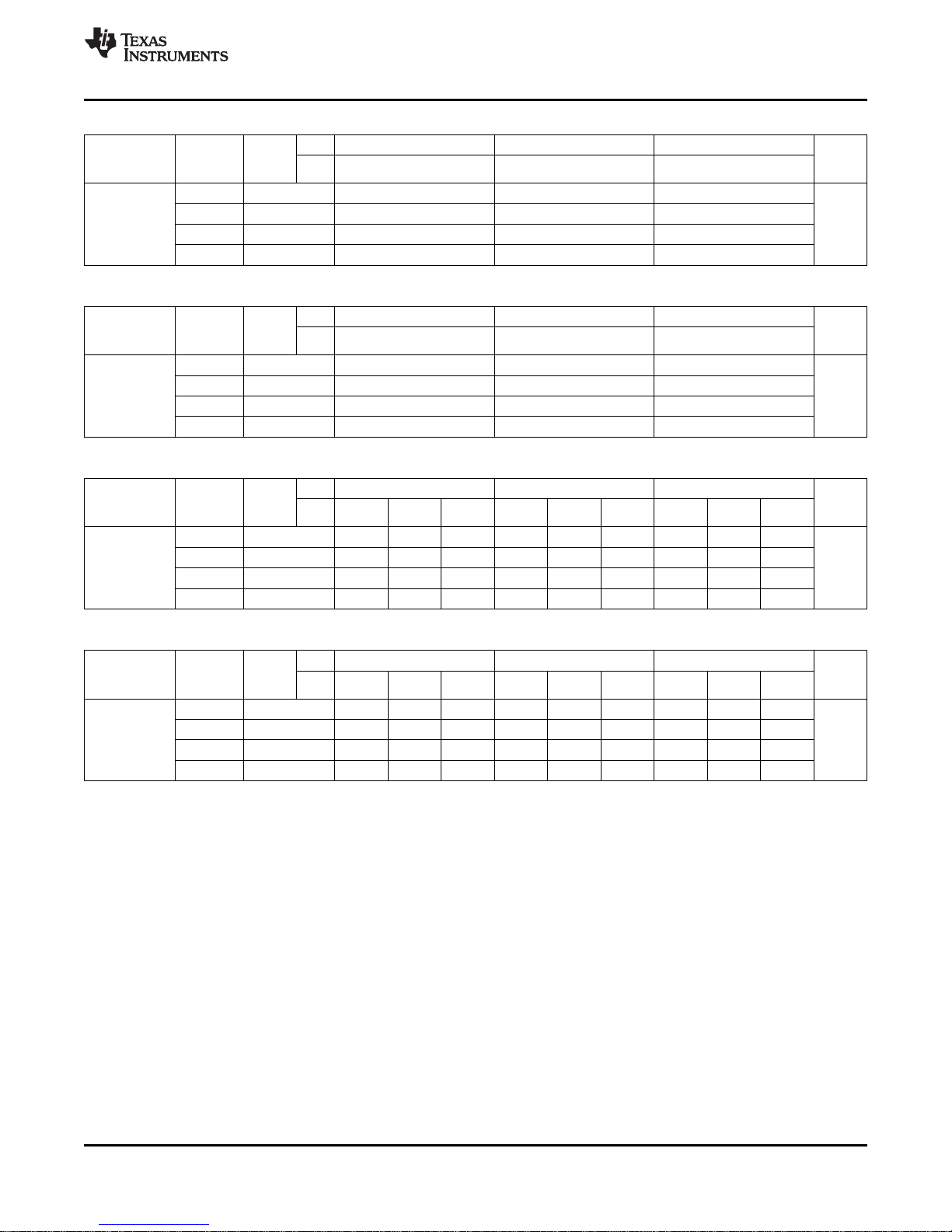
ECCN 5E002 TSPA - Technology / Software Publicly Available
CC430F6137, CC430F6135, CC430F6127, CC430F6126, CC430F6125
CC430F5137, CC430F5135, CC430F5133
www.ti.com
Typical TX Current Consumption, 315 MHz
PARAMETER Power UNIT
Current
consumption, mA
TX
PATABLE
Setting
0xC0 max. 27.5 26.4 28.1
0xC4 +10 25.1 25.2 25.3
0x51 0 14.4 14.6 14.7
0x29 -6 14.2 14.7 15.0
Output V
(dBm)
CC
T
A
2.0 V 3.0 V 3.6 V
25°C 25°C 25°C
Typical TX Current Consumption, 433 MHz
PARAMETER Power UNIT
Current
consumption, mA
TX
PATABLE
Setting
0xC0 max. 33.1 33.4 33.8
0xC6 +10 28.6 28.8 28.8
0x50 0 16.6 16.8 16.9
0x2D -6 16.8 17.5 17.8
Output V
(dBm)
CC
T
A
2.0 V 3.0 V 3.6 V
25°C 25°C 25°C
Typical TX Current Consumption, 868 MHz
PARAMETER Power UNIT
Current
consumption, mA
TX
PATABLE
Setting
0xC0 max. 36.7 35.2 34.2 38.5 35.5 34.9 37.1 35.7 34.7
0xC3 +10 34.0 32.8 32.0 34.2 33.0 32.5 34.3 33.1 32.2
0x8D 0 18.0 17.6 17.5 18.3 17.8 18.1 18.4 18.0 17.7
0x2D -6 17.1 17.0 17.2 17.8 17.8 18.3 18.2 18.1 18.1
Output V
(dBm)
CC
TA-40°C 25°C 85°C -40°C 25°C 85°C -40°C 25°C 85°C
2.0 V 3.0 V 3.6 V
SLAS554H –MAY 2009–REVISED SEPTEMBER 2013
Typical TX Current Consumption, 915 MHz
PARAMETER Power UNIT
Current
consumption, mA
TX
PATABLE
Setting
0xC0 max. 35.5 33.8 33.2 36.2 34.8 33.6 36.3 35.0 33.8
0xC3 +10 33.2 32.0 31.0 33.4 32.1 31.2 33.5 32.3 31.3
0x8D 0 17.8 17.4 17.1 18.1 17.6 17.3 18.2 17.8 17.5
0x2D -6 17.0 16.9 16.9 17.7 17.6 17.6 18.1 18.0 18.0
Output V
(dBm)
CC
TA-40°C 25°C 85°C -40°C 25°C 85°C -40°C 25°C 85°C
2.0 V 3.0 V 3.6 V
Copyright © 2009–2013, Texas Instruments Incorporated Submit Documentation Feedback 75
Product Folder Links: CC430F6137 CC430F6135 CC430F6127 CC430F6126 CC430F6125 CC430F5137
CC430F5135 CC430F5133
Page 76

ECCN 5E002 TSPA - Technology / Software Publicly Available
CC430F6137, CC430F6135, CC430F6127, CC430F6126, CC430F6125
CC430F5137, CC430F5135, CC430F5133
SLAS554H –MAY 2009–REVISED SEPTEMBER 2013
RF Receive, Overall
TA= 25°C, VCC= 3 V (unless otherwise noted)
PARAMETER TEST CONDITIONS MIN TYP MAX UNIT
Digital channel filter bandwidth
Spurious emissions
RX latency Serial operation
(1) All measurement results are obtained using the EM430F6137RF900 with BOM according to tested frequency range (see Table 48).
(2) User programmable. The bandwidth limits are proportional to crystal frequency (given values assume a 26.0 MHz crystal)
(3) Typical radiated spurious emission is -49 dBm measured at the VCO frequency
(4) Maximum figure is the ETSI EN 300 220 limit
(5) Time from start of reception until data is available on the receiver data output pin is equal to 9 bit.
(3) (4)
(2)
25 MHz to 1 GHz -68 -57
Above 1 GHz -66 -47
(1)
58 812 kHz
(5)
RF Receive, 315 MHz
TA= 25°C, VCC= 3 V (unless otherwise noted)
2-FSK, 1% packet error rate, 20-byte packet length, Sensitivity optimized, MDMCFG2.DEM_DCFILT_OFF = 0 (unless
otherwise noted)
PARAMETER TEST CONDITIONS MIN TYP MAX UNIT
Receiver sensitivity 38.4 20kHz deviation, 100kHz digital channel filter bandwidth
(1) All measurement results are obtained using the EM430F6137RF900 with BOM according to tested frequency range (see Table 48).
(2) Sensitivity can be traded for current consumption by setting MDMCFG2.DEM_DCFILT_OFF=1. The typical current consumption is then
reduced by about 2mA close to the sensitivity limit. The sensitivity is typically reduced to -109dBm.
(3) Sensitivity can be traded for current consumption by setting MDMCFG2.DEM_DCFILT_OFF=1. The typical current consumption is then
reduced by about 2mA close to the sensitivity limit. The sensitivity is typically reduced to -102dBm.
(4) MDMCFG2.DEM_DCFILT_OFF=1 can not be used for data rates ≥ 250kBaud.
DATA RATE
(kBaud)
0.6 14.3kHz deviation, 58kHz digital channel filter bandwidth -117
1.2 5.2kHz deviation, 58kHz digital channel filter bandwidth
250 127kHz deviation, 540kHz digital channel filter bandwidth
500 MSK, 812kHz digital channel filter bandwidth
(1)
(2)
(3)
(4)
(4)
-111
-103 dBm
-95
-86
www.ti.com
dBm
9 bit
RF Receive, 433 MHz
TA= 25°C, VCC= 3 V (unless otherwise noted)
2-FSK, 1% packet error rate, 20-byte packet length, Sensitivity optimized, MDMCFG2.DEM_DCFILT_OFF = 0 (unless
otherwise noted)
PARAMETER TEST CONDITIONS MIN TYP MAX UNIT
Receiver sensitivity dBm
(1) All measurement results are obtained using the EM430F6137RF900 with BOM according to tested frequency range (see Table 48).
(2) Sensitivity can be traded for current consumption by setting MDMCFG2.DEM_DCFILT_OFF=1. The typical current consumption is then
reduced by about 2mA close to the sensitivity limit. The sensitivity is typically reduced to -109dBm.
(3) Sensitivity can be traded for current consumption by setting MDMCFG2.DEM_DCFILT_OFF=1. The typical current consumption is then
reduced by about 2mA close to the sensitivity limit. The sensitivity is typically reduced to -101dBm.
(4) MDMCFG2.DEM_DCFILT_OFF=1 can not be used for data rates ≥ 250kBaud.
DATA RATE
(kBaud)
0.6 14.3kHz deviation, 58kHz digital channel filter bandwidth -114
1.2 5.2-kHz deviation, 58-kHz digital channel filter bandwidth
38.4 20-kHz deviation, 100-kHz digital channel filter bandwidth
250 -93
500 MSK, 812kHz digital channel filter bandwidth
(1)
127-kHz deviation, 540-kHz digital channel filter bandwidth
(4)
(4)
(2)
(3)
-111
-104
-85
76 Submit Documentation Feedback Copyright © 2009–2013, Texas Instruments Incorporated
Product Folder Links: CC430F6137 CC430F6135 CC430F6127 CC430F6126 CC430F6125 CC430F5137
CC430F5135 CC430F5133
Page 77
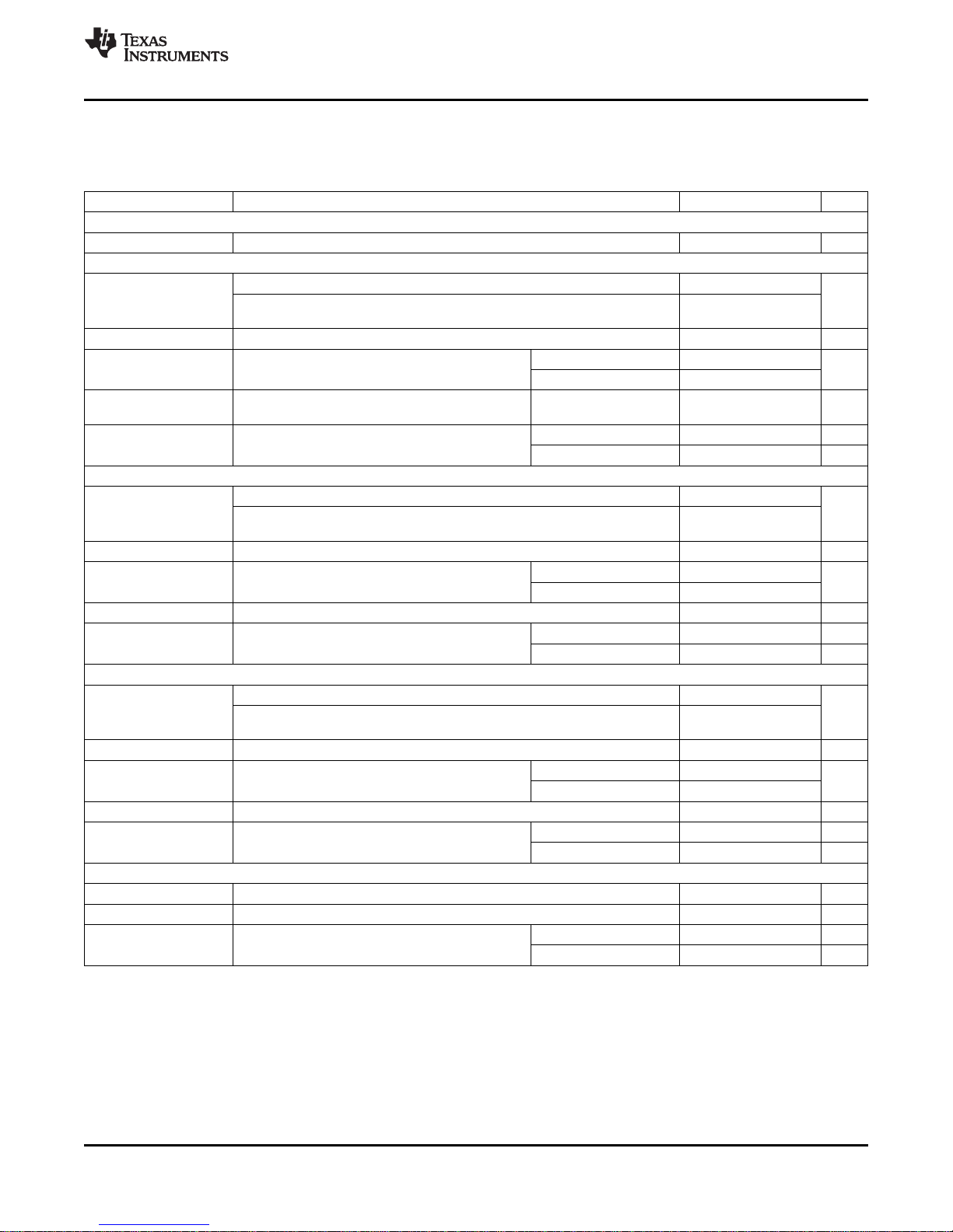
ECCN 5E002 TSPA - Technology / Software Publicly Available
CC430F6137, CC430F6135, CC430F6127, CC430F6126, CC430F6125
CC430F5137, CC430F5135, CC430F5133
www.ti.com
RF Receive, 868 or 915 MHz
TA= 25°C, VCC= 3 V (unless otherwise noted)
1% packet error rate, 20-byte packet length, Sensitivity optimized, MDMCFG2.DEM_DCFILT_OFF = 0 (unless otherwise
noted)
PARAMETER TEST CONDITIONS MIN TYP MAX UNIT
0.6-kBaud data rate, 2-FSK, 14.3-kHz deviation, 58-kHz digital channel filter bandwidth (unless otherwise noted)
Receiver sensitivity -115 dBm
1.2-kBaud data rate, 2-FSK, 5.2-kHz deviation, 58-kHz digital channel filter bandwidth (unless otherwise noted)
Receiver sensitivity
Saturation FIFOTHR.CLOSE_IN_RX=0
Adjacent channel Desired channel 3 dB above the sensitivity limit,
rejection 100 kHz channel spacing
Image channel rejection 29 dB
Blocking Desired channel 3 dB above the sensitivity limit
38.4-kBaud data rate, 2-FSK, 20-kHz deviation, 100-kHz digital channel filter bandwidth (unless otherwise noted)
Receiver sensitivity
Saturation FIFOTHR.CLOSE_IN_RX=0
Adjacent channel Desired channel 3 dB above the sensitivity limit, -200-kHz offset 20
rejection 200 kHz channel spacing
Image channel rejection IF frequency 152 kHz, Desired channel 3 dB above the sensitivity limit 23 dB
Blocking Desired channel 3 dB above the sensitivity limit
250-kBaud data rate, 2-FSK, 127-kHz deviation, 540-kHz digital channel filter bandwidth (unless otherwise noted)
Receiver sensitivity
Saturation FIFOTHR.CLOSE_IN_RX=0
Adjacent channel Desired channel 3 dB above the sensitivity limit, -750-kHz offset 24
rejection 750-kHz channel spacing
Image channel rejection IF frequency 304 kHz, Desired channel 3 dB above the sensitivity limit 18 dB
Blocking Desired channel 3 dB above the sensitivity limit
500-kBaud data rate, MSK, 812-kHz digital channel filter bandwidth (unless otherwise noted)
Receiver sensitivity
Image channel rejection IF frequency 355 kHz, Desired channel 3 dB above the sensitivity limit -2 dB
Blocking Desired channel 3 dB above the sensitivity limit
(1) All measurement results are obtained using the EM430F6137RF900 with BOM according to tested frequency range (see Table 48).
(2) Sensitivity can be traded for current consumption by setting MDMCFG2.DEM_DCFILT_OFF=1. The typical current consumption is then
reduced by about 2mA close to the sensitivity limit. The sensitivity is typically reduced to -107dBm
(3) See design note DN010 Close-in Reception with CC1101 (SWRA147).
(4) See Figure 22 for blocking performance at other offset frequencies.
(5) See Figure 23 for blocking performance at other offset frequencies.
(6) Sensitivity can be traded for current consumption by setting MDMCFG2.DEM_DCFILT_OFF=1. The typical current consumption is then
reduced by about 2mA close to the sensitivity limit. The sensitivity is typically reduced to -100dBm.
(7) MDMCFG2.DEM_DCFILT_OFF = 1 cannot be used for data rates ≥ 250kBaud.
(8) See Figure 24 for blocking performance at other offset frequencies.
(9) See Figure 25 for blocking performance at other offset frequencies.
(2)
2-GFSK modulation by setting MDMCFG2.MOD_FORMAT=2,
Gaussian filter with BT = 0.5
IF frequency 152 kHz, desired channel 3 dB above
the sensitivity limit
(6)
2-GFSK modulation by setting MDMCFG2.MOD_FORMAT = 2,
Gaussian filter with BT = 0.5
(7)
2-GFSK modulation by setting MDMCFG2.MOD_FORMAT = 2,
Gaussian filter with BT = 0.5
(7)
(1)
(3)
(4)
-100-kHz offset 39
+100-kHz offset 39
±2 MHz offset -48 dBm
(5)
±10 MHz offset -40 dBm
(3)
(5)
+200-kHz offset 25
(5)
±2-MHz offset -48 dBm
±10-MHz offset -40 dBm
(3)
(8)
+750-kHz offset 30
(8)
±2-MHz offset -53 dBm
±10-MHz offset -39 dBm
(9)
±2-MHz offset -53 dBm
±10-MHz offset -38 dBm
SLAS554H –MAY 2009–REVISED SEPTEMBER 2013
-109
-109
dBm
-28 dBm
dB
-102
-101
dBm
-19 dBm
dB
-90
-90
dBm
-19 dBm
dB
-84 dBm
Copyright © 2009–2013, Texas Instruments Incorporated Submit Documentation Feedback 77
Product Folder Links: CC430F6137 CC430F6135 CC430F6127 CC430F6126 CC430F6125 CC430F5137
CC430F5135 CC430F5133
Page 78
-20
-10
0
10
20
30
40
50
60
70
80
-40 -30 -20 -10 0 10 20 30 40
Offset [M Hz]
Blocking [dB]
-20
-10
0
10
20
30
40
50
-1 -0.8 -0.6 -0.4 -0.2 0 0.2 0.4 0.6 0.8 1
Offset [M Hz]
Selectivity [dB]
-20
-10
0
10
20
30
40
50
60
70
80
-40 -30 -20 -10 0 10 20 30 40
Offset [M Hz]
Blocking [dB]
-10
0
10
20
30
40
50
60
-1 -0.8 -0.6 -0.4 -0.2 0 0.2 0.4 0.6 0.8 1
Offset [M Hz]
Selectivity [dB]
ECCN 5E002 TSPA - Technology / Software Publicly Available
CC430F6137, CC430F6135, CC430F6127, CC430F6126, CC430F6125
CC430F5137, CC430F5135, CC430F5133
SLAS554H –MAY 2009–REVISED SEPTEMBER 2013
www.ti.com
NOTE: 868.3 MHz, 2-FSK, 5.2-kHz deviation, IF frequency is 152.3 kHz, digital channel filter bandwidth is 58 kHz
Figure 22. Typical Selectivity at 1.2-kBaud Data Rate
NOTE: 868 MHz, 2-FSK, 20 kHz deviation, IF frequency is 152.3 kHz, digital channel filter bandwidth is 100 kHz
Figure 23. Typical Selectivity at 38.4-kBaud Data Rate
78 Submit Documentation Feedback Copyright © 2009–2013, Texas Instruments Incorporated
Product Folder Links: CC430F6137 CC430F6135 CC430F6127 CC430F6126 CC430F6125 CC430F5137
CC430F5135 CC430F5133
Page 79
-20
-10
0
10
20
30
40
50
60
70
80
-40 -30 -20 -10 0 10 20 30 40
Offset [M Hz]
Blocking [dB]
-20
-10
0
10
20
30
40
50
-3 -2 -1 0 1 2 3
Offset [M Hz]
Selectivity [dB]
-20
-10
0
10
20
30
40
50
60
70
80
-40 -30 -20 -10 0 10 20 30 40
Offset [M Hz]
Blocking [dB]
-20
-10
0
10
20
30
40
50
-3 -2 -1 0 1 2 3
Offset [M Hz]
Selectivity [dB]
www.ti.com
ECCN 5E002 TSPA - Technology / Software Publicly Available
CC430F6137, CC430F6135, CC430F6127, CC430F6126, CC430F6125
CC430F5137, CC430F5135, CC430F5133
SLAS554H –MAY 2009–REVISED SEPTEMBER 2013
NOTE: 868 MHz, 2-FSK, IF frequency is 304 kHz, digital channel filter bandwidth is 540 kHz
Figure 24. Typical Selectivity at 250-kBaud Data Rate
NOTE: 868 MHz, 2-FSK, IF frequency is 355 kHz, digital channel filter bandwidth is 812 kHz
Figure 25. Typical Selectivity at 500-kBaud Data Rate
Copyright © 2009–2013, Texas Instruments Incorporated Submit Documentation Feedback 79
Product Folder Links: CC430F6137 CC430F6135 CC430F6127 CC430F6126 CC430F6125 CC430F5137
CC430F5135 CC430F5133
Page 80

ECCN 5E002 TSPA - Technology / Software Publicly Available
CC430F6137, CC430F6135, CC430F6127, CC430F6126, CC430F6125
CC430F5137, CC430F5135, CC430F5133
SLAS554H –MAY 2009–REVISED SEPTEMBER 2013
Typical Sensitivity, 315 MHz, Sensitivity Optimized Setting
V
PARAMETER DATA RATE (kBaud) UNIT
Sensitivity,
315MHz
1.2 -112 -112 -110 -112 -111 -109 -112 -111 -108
38.4 -105 -105 -104 -105 -103 -102 -105 -104 -102 dBm
250 -95 -95 -92 -94 -95 -92 -95 -94 -91
CC
TA-40°C 25°C 85°C -40°C 25°C 85°C -40°C 25°C 85°C
2.0 V 3.0 V 3.6 V
Typical Sensitivity, 433 MHz, Sensitivity Optimized Setting
V
PARAMETER DATA RATE (kBaud) UNIT
Sensitivity,
433MHz
1.2 -111 -110 -108 -111 -111 -108 -111 -110 -107
38.4 -104 -104 -101 -104 -104 -101 -104 -103 -101 dBm
250 -93 -94 -91 -93 -93 -90 -93 -93 -90
CC
TA-40°C 25°C 85°C -40°C 25°C 85°C -40°C 25°C 85°C
2.0 V 3.0 V 3.6 V
Typical Sensitivity, 868 MHz, Sensitivity Optimized Setting
V
PARAMETER DATA RATE (kBaud) UNIT
1.2 -109 -109 -107 -109 -109 -106 -109 -108 -106
Sensitivity,
868MHz
38.4 -102 -102 -100 -102 -102 -99 -102 -101 -99
250 -90 -90 -88 -89 -90 -87 -89 -90 -87
500 -84 -84 -81 -84 -84 -80 -84 -84 -80
CC
TA-40°C 25°C 85°C -40°C 25°C 85°C -40°C 25°C 85°C
2.0 V 3.0 V 3.6 V
www.ti.com
dBm
Typical Sensitivity, 915 MHz, Sensitivity Optimized Setting
V
PARAMETER DATA RATE (kBaud) UNIT
1.2 -109 -109 -107 -109 -109 -106 -109 -108 -105
Sensitivity,
915MHz
38.4 -102 -102 -100 -102 -102 -99 -103 -102 -99
250 -92 -92 -89 -92 -92 -88 -92 -92 -88
500 -87 -86 -81 -86 -86 -81 -86 -85 -80
CC
TA-40°C 25°C 85°C -40°C 25°C 85°C -40°C 25°C 85°C
2.0 V 3.0 V 3.6 V
dBm
80 Submit Documentation Feedback Copyright © 2009–2013, Texas Instruments Incorporated
Product Folder Links: CC430F6137 CC430F6135 CC430F6127 CC430F6126 CC430F6125 CC430F5137
CC430F5135 CC430F5133
Page 81
ECCN 5E002 TSPA - Technology / Software Publicly Available
CC430F6137, CC430F6135, CC430F6127, CC430F6126, CC430F6125
CC430F5137, CC430F5135, CC430F5133
www.ti.com
RF Transmit
TA= 25°C, VCC= 3 V (unless otherwise noted)
PTX= +10 dBm (unless otherwise noted)
PARAMETER TEST CONDITIONS MIN TYP MAX UNIT
Differential load
impedance
Output power, highest Delivered to a 50Ω single-ended load via CC430
setting
Output power, lowest Delivered to a 50Ω single-ended load via CC430
setting
Harmonics,
radiated
Harmonics, conducted dBm
Spurious emissions,
conducted, harmonics dBm
not included
(2)
(3)
(3)
(4)(5)(6)
(8)
FREQUENCY
(MHz)
315 122 + j31
433 116 + j41 Ω
868, 915 86.5 + j43
315 +12
433 +13
868 +11
915 +11
433
868 dBm
915
315 +10 dBm CW
433 +10 dBm CW
868 +10 dBm CW
915 +11 dBm CW
315 +10 dBm CW
433 +10 dBm CW
868 +10 dBm CW
915 +11 dBm CW
(1)
reference design's RF matching network
reference design's RF matching network
Second harmonic -56
Third harmonic -57
Second harmonic -50
Third harmonic -52
Second harmonic -50
Third harmonic -54
Frequencies below 960 MHz < -38
Frequencies above 960 MHz < -48
Frequencies below 1 GHz -45
Frequencies above 1 GHz < -48
Second harmonic -59
Other harmonics < -71
Second harmonic -53
Other harmonics < -47
Frequencies below 960 MHz < -58
Frequencies above 960 MHz < -53
Frequencies below 1 GHz < -54
Frequencies above 1 GHz < -54
Frequencies within 47 to 74, 87.5 to
118, 174 to 230, 470 to 862 MHz
Frequencies below 1 GHz < -46
Frequencies above 1 GHz < -59
Frequencies within 47 to 74, 87.5 to
118, 174 to 230, 470 to 862 MHz
Frequencies below 960 MHz < -49
Frequencies above 960 MHz < -63
SLAS554H –MAY 2009–REVISED SEPTEMBER 2013
dBm
-30 dBm
(7)
< -63
< -56
(1) All measurement results are obtained using the EM430F6137RF900 with BOM according to tested frequency range (see Table 48).
(2) Differential impedance as seen from the RF-port (RF_P and RF_N) towards the antenna. Follow the CC430 reference designs available
from the TI website.
(3) Output power is programmable, and full range is available in all frequency bands. Output power may be restricted by regulatory limits.
See also application note AN050 Using the CC1101 in the European 868MHz SRD Band (SWRA146) and design note DN013
Programming Output Power on CC1101 (SWRA168), which gives the output power and harmonics when using multi-layer inductors.
The output power is then typically +10 dBm when operating at 868 or 915 MHz.
(4) The antennas used during the radiated measurements (SMAFF-433 from R.W.Badland and Nearson S331 868/915) play a part in
attenuating the harmonics.
(5) Measured on EM430F6137RF900 with CW, maximum output power
(6) All harmonics are below -41.2 dBm when operating in the 902 to 928 MHz band.
(7) Requirement is -20 dBc under FCC 15.247
(8) All radiated spurious emissions are within the limits of ETSI. Also see design note DN017 CC11xx 868/915 MHz RF Matching
(SWRA168).
Copyright © 2009–2013, Texas Instruments Incorporated Submit Documentation Feedback 81
Product Folder Links: CC430F6137 CC430F6135 CC430F6127 CC430F6126 CC430F6125 CC430F5137
CC430F5135 CC430F5133
Page 82

ECCN 5E002 TSPA - Technology / Software Publicly Available
CC430F6137, CC430F6135, CC430F6127, CC430F6126, CC430F6125
CC430F5137, CC430F5135, CC430F5133
SLAS554H –MAY 2009–REVISED SEPTEMBER 2013
RF Transmit (continued)
TA= 25°C, VCC= 3 V (unless otherwise noted)
PTX= +10 dBm (unless otherwise noted)
PARAMETER TEST CONDITIONS MIN TYP MAX UNIT
TX latency
(9) Time from sampling the data on the transmitter data input pin until it is observed on the RF output ports
(9)
FREQUENCY
(MHz)
(1)
Serial operation 8 bits
Optimum PATABLE Settings for Various Output Power Levels and Frequency Bands
TA= 25°C, VCC= 3 V (unless otherwise noted)
Output Power (dBm)
-30 0x12 0x05 0x03 0x03
-12 0x33 0x26 0x25 0x25
-6 0x29 0x2D 0x2D 0x2D
0 0x51 0x50 0x8D 0x8D
10 0xC4 0xC4 0xC3 0xC3
Maximum 0xC0 0xC0 0xC0 0xC0
(1) All measurement results are obtained using the EM430F6137RF900 with BOM according to tested frequency range (see Table 48).
315 MHz 433 MHz 868 MHz 915 MHz
(1)
PATABLE Setting
www.ti.com
82 Submit Documentation Feedback Copyright © 2009–2013, Texas Instruments Incorporated
Product Folder Links: CC430F6137 CC430F6135 CC430F6127 CC430F6126 CC430F6125 CC430F5137
CC430F5135 CC430F5133
Page 83

ECCN 5E002 TSPA - Technology / Software Publicly Available
CC430F6137, CC430F6135, CC430F6127, CC430F6126, CC430F6125
CC430F5137, CC430F5135, CC430F5133
www.ti.com
Typical Output Power, 315 MHz
PARAMETER PATABLE Setting UNIT
0xC0 (max) 11.9 11.8 11.8
Output power,
315 MHz
(1) All measurement results are obtained using the EM430F6137RF900 with BOM according to tested frequency range (see Table 48).
0xC4 (10 dBm) 10.3 10.3 10.3
0xC6 (default) 9.3 dBm
0x51 (0 dBm) 0.7 0.6 0.7
0x29 (-6 dBm) -6.8 -5.6 -5.3
(1)
V
CC
TA-40°C 25°C 85°C -40°C 25°C 85°C -40°C 25°C 85°C
2.0 V 3.0 V 3.6 V
SLAS554H –MAY 2009–REVISED SEPTEMBER 2013
Typical Output Power, 433 MHz
PARAMETER PATABLE Setting UNIT
0xC0 (max) 12.6 12.6 12.6
Output power,
433 MHz
(1) All measurement results are obtained using the EM430F6137RF900 with BOM according to tested frequency range (see Table 48).
0xC4 (10 dBm) 10.3 10.2 10.2
0xC6 (default) 10.0 dBm
0x50 (0 dBm) 0.3 0.3 0.3
0x2D (-6 dBm) -6.4 -5.4 -5.1
Typical Output Power, 868 MHz
PARAMETER PATABLE Setting UNIT
0xC0 (max) 11.9 11.2 10.5 11.9 11.2 10.5 11.9 11.2 10.5
Output power,
868 MHz
(1) All measurement results are obtained using the EM430F6137RF900 with BOM according to tested frequency range (see Table 48).
0xC3 (10 dBm) 10.8 10.1 9.4 10.8 10.1 9.4 10.7 10.1 9.4
0xC6 (default) 8.8 dBm
0x8D (0 dBm) 1.0 0.3 -0.3 1.1 0.3 -0.3 1.1 0.3 -0.3
0x2D (-6 dBm) -6.5 -6.8 -7.3 -5.3 -5.8 -6.3 -4.9 -5.4 -6.0
Typical Output Power, 915 MHz
PARAMETER PATABLE Setting UNIT
0xC0 (max) 12.2 11.4 10.6 12.1 11.4 10.7 12.1 11.4 10.7
Output power,
915 MHz
(1) All measurement results are obtained using the EM430F6137RF900 with BOM according to tested frequency range (see Table 48).
0xC3 (10 dBm) 11.0 10.3 9.5 11.0 10.3 9.5 11.0 10.3 9.6
0xC6 (default) 8.8 dBm
0x8D (0 dBm) 1.9 1.0 0.3 1.9 1.0 0.3 1.9 1.1 0.3
0x2D (-6 dBm) -5.5 -6.0 -6.5 -4.3 -4.8 -5.5 -3.9 -4.4 -5.1
(1)
V
CC
TA-40°C 25°C 85°C -40°C 25°C 85°C -40°C 25°C 85°C
(1)
V
CC
TA-40°C 25°C 85°C -40°C 25°C 85°C -40°C 25°C 85°C
(1)
V
CC
TA-40°C 25°C 85°C -40°C 25°C 85°C -40°C 25°C 85°C
2.0 V 3.0 V 3.6 V
2.0 V 3.0 V 3.6 V
2.0 V 3.0 V 3.6 V
Copyright © 2009–2013, Texas Instruments Incorporated Submit Documentation Feedback 83
Product Folder Links: CC430F6137 CC430F6135 CC430F6127 CC430F6126 CC430F6125 CC430F5137
CC430F5135 CC430F5133
Page 84

ECCN 5E002 TSPA - Technology / Software Publicly Available
CC430F6137, CC430F6135, CC430F6127, CC430F6126, CC430F6125
CC430F5137, CC430F5135, CC430F5133
SLAS554H –MAY 2009–REVISED SEPTEMBER 2013
Frequency Synthesizer Characteristics
TA= 25°C, VCC= 3 V (unless otherwise noted)
MIN figures are given using a 27MHz crystal. TYP and MAX figures are given using a 26MHz crystal.
PARAMETER TEST CONDITIONS MIN TYP MAX UNIT
Programmed frequency resolution
Synthesizer frequency tolerance
RF carrier phase noise dBc/Hz
PLL turn-on and hop time
PLL RX to TX settling time
PLL TX to RX settling time
PLL calibration time
(7)
(1) All measurement results are obtained using the EM430F6137RF900 with BOM according to tested frequency range (see Table 48).
(2) The resolution (in Hz) is equal for all frequency bands.
(3) Depends on crystal used. Required accuracy (including temperature and aging) depends on frequency band and channel bandwidth and
spacing.
(4) Time from leaving the IDLE state until arriving in the RX, FSTXON, or TX state, when not performing calibration.
(5) Settling time for the 1-IF frequency step from RX to TX
(6) Settling time for the 1-IF frequency step from TX to RX
(7) Calibration can be initiated manually or automatically before entering or after leaving RX or TX.
(2)
(3)
(4)
(5)
(6)
(1)
26- to 27-MHz crystal 397 f
XOSC
16
/2
±40 ppm
50-kHz offset from carrier –95
100-kHz offset from carrier –94
200-kHz offset from carrier –94
500-kHz offset from carrier –98
1-MHz offset from carrier –107
2-MHz offset from carrier –112
5-MHz offset from carrier –118
10-MHz offset from carrier –129
Crystal oscillator running 85.1 88.4 88.4 µs
9.3 9.6 9.6 µs
20.7 21.5 21.5 µs
694 721 721 µs
www.ti.com
412 Hz
84 Submit Documentation Feedback Copyright © 2009–2013, Texas Instruments Incorporated
Product Folder Links: CC430F6137 CC430F6135 CC430F6127 CC430F6126 CC430F6125 CC430F5137
CC430F5135 CC430F5133
Page 85

-120
-100
-80
-60
-40
-20
0
-120 -100 -80 -60 -40 -20 0
Input Pow e r [dBm]
RSSI Readout [dBm]
1.2kBaud
38.4kBaud
-120
-100
-80
-60
-40
-20
0
-120 -100 -80 -60 -40 -20 0
Input Pow e r [dBm]
RSSI Readout [dBm]
250kBaud
500kBaud
ECCN 5E002 TSPA - Technology / Software Publicly Available
CC430F6137, CC430F6135, CC430F6127, CC430F6126, CC430F6125
CC430F5137, CC430F5135, CC430F5133
www.ti.com
Typical RSSI_offset Values
TA= 25°C, VCC= 3 V (unless otherwise noted)
DATA RATE (kBaud)
1.2 74 74
38.4 74 74
250 74 74
500 74 74
(1) All measurement results are obtained using the EM430F6137RF900 with BOM according to tested frequency range (see Table 48).
(1)
RSSI_OFFSET (dB)
433 MHz 868 MHz
SLAS554H –MAY 2009–REVISED SEPTEMBER 2013
Figure 26. Typical RSSI Value vs Input Power Level for Different Data Rates at 868 MHz
Copyright © 2009–2013, Texas Instruments Incorporated Submit Documentation Feedback 85
Product Folder Links: CC430F6137 CC430F6135 CC430F6127 CC430F6126 CC430F6125 CC430F5137
CC430F5135 CC430F5133
Page 86

RF_N
RF_P
AVCC_RF
AVCC_RF
AVCC_RF
AVCC_RF
GUARD
C5
C6
C7
C3
C2
C1
C4
R1
C23
L1
L6
L5
L4
L3
L2
C29
C28
C27
C24
C25
C26
L7
SMA STRAIGHT JACK, SMT
R_BIAS
26MHz
C22
C21
RF_XOUT
RF_XIN
VDD
C9
C8
DVCC
VDD
C11
C10
C19
DVCC
VCORE
TDO
TDI/TCLK
TMS
(JTAG / SBW signals)
AVDD
C16
C17
C18
VDD
C14
C15
R2
C20
DVCC
nRST/NMI/SBWTDIO
TCK
TEST/SBWTCK
AVDD
C12
C13
AVCC
AVSS
(May be added close to the respective pins
to reduce emissions at 5GHz to levels
required by ETSI.)
CC430F61xx
17
64
18
63
19
62
20
61
21
60
22
59
29
52
30
51
31
50
32
49
23
58
24
57
25
56
26
55
27
54
28
53
3316341535143613371238
11
45446347248
1
391040941842743644
5
ECCN 5E002 TSPA - Technology / Software Publicly Available
CC430F6137, CC430F6135, CC430F6127, CC430F6126, CC430F6125
CC430F5137, CC430F5135, CC430F5133
SLAS554H –MAY 2009–REVISED SEPTEMBER 2013
APPLICATION CIRCUIT
www.ti.com
For a complete reference design including layout see the CC430 Wireless Development Tools and related
documentation [MSP430 Hardware Tools User's Guide (SLAU278)].
Figure 27. Typical Application Circuit CC430F61xx
86 Submit Documentation Feedback Copyright © 2009–2013, Texas Instruments Incorporated
Product Folder Links: CC430F6137 CC430F6135 CC430F6127 CC430F6126 CC430F6125 CC430F5137
CC430F5135 CC430F5133
Page 87

RF_N
RF_P
AVCC_RF
AVCC_RF
AVCC_RF
AVCC_RF
GUARD
C5
C6
C7
C3
C2
C1
C4
R1
C23
L1
L6
L5
L4
L3
L2
C29
C28
C27
C24
C25
C26
L7
SMA STRAIGHT JACK, SMT
R_BIAS
26MHz
C22
C21
RF_XOUT
RF_XIN
VDD
C9
C8
DVCC
VDD
C11
C10
DVCC
VCORE
TDO
TDI/TCLK
(JTAG / SBW signals)
AVDD
C16
C17
C18
VDD
C14
C15
R2
C20
DVCC
nRST/NMI/SBWTDIO
TCK
TEST/SBWTCK
AVDD
C12
C13
AVCC
TMS
AVSS
12
11
4
3
2
1
10
9
8
7
6
5
13
14 15 16
17 18
19
20
21 22
23
24
25
26
27
28
29
30
31
32
33
34
35
36
48
47 46 45
44 43
42
41
40 39
38
37
CC430F51xx
(May be added close to the respective pins
to reduce emissions at 5GHz to levels
required by ETSI.)
www.ti.com
ECCN 5E002 TSPA - Technology / Software Publicly Available
CC430F6137, CC430F6135, CC430F6127, CC430F6126, CC430F6125
CC430F5137, CC430F5135, CC430F5133
SLAS554H –MAY 2009–REVISED SEPTEMBER 2013
For a complete reference design including layout see the CC430 Wireless Development Tools and related
documentation [MSP430 Hardware Tools User's Guide (SLAU278)].
Figure 28. Typical Application Circuit CC430F51xx
Copyright © 2009–2013, Texas Instruments Incorporated Submit Documentation Feedback 87
Product Folder Links: CC430F6137 CC430F6135 CC430F6127 CC430F6126 CC430F6125 CC430F5137
CC430F5135 CC430F5133
Page 88

ECCN 5E002 TSPA - Technology / Software Publicly Available
CC430F6137, CC430F6135, CC430F6127, CC430F6126, CC430F6125
CC430F5137, CC430F5135, CC430F5133
SLAS554H –MAY 2009–REVISED SEPTEMBER 2013
Table 48. Bill of Materials
Components For 315 MHz For 433 MHz For 868, 915 MHz Comment
C1,3,4,5,7,9,11,13,15 100 nF Decoupling capacitors
C8,10,12,14 10 µF Decoupling capacitors
C2,6,16,17,18 2 pF Decoupling capacitors
C19 470 nF V
C20 2.2 nF
C21,22 27 pF
R1 56 kΩ R_BIAS (±1% required)
R2 47 kΩ RST pullup
L1,2 Capacitors: 220 pF 0.016 µH 0.012 µH
L3,4 0.033 µH 0.027 µH 0.018 µH
L5 0.033 µH 0.047 µH 0.015 µH
L6 dnp
L7 0.033 µH 0.051 µH 0.015 µH
C23 dnp
C24 220 pF 220 pF 100 pF
C25 6.8 pF 3.9 pF 1.5 pF
C26 6.8 pF 3.9 pF 1.5 pF
C27 220 pF 220 pF 1.5 pF
C28 10 pF 4.7 pF 8.2 pF
C29 220 pF 220 pF 1.5 pF
(1) The load capacitance CLseen by the crystal is CL= 1/((1/C21)+(1/C22)) + C
capacitance and PCB stray capacitance. It can be typically estimated to be approximately 2.5 pF.
(2) dnp = do not populate
(2)
(2)
(2)
dnp
2.7 pF 1 pF
. The parasitic capacitance C
parasitic
0.0022 µH
CORE
RST decoupling cap
(optimized for SBW)
Load capacitors for
26 MHz crystal
parasitic
www.ti.com
capacitor
includes pin
(1)
88 Submit Documentation Feedback Copyright © 2009–2013, Texas Instruments Incorporated
Product Folder Links: CC430F6137 CC430F6135 CC430F6127 CC430F6126 CC430F6125 CC430F5137
CC430F5135 CC430F5133
Page 89

P1.0/P1MAP0(/S18)
P1.1/P1MAP1(/S19)
P1.2/P1MAP2(/S20)
P1.3/P1MAP3(/S21)
P1.4/P1MAP4(/S22)
Direction
0:Input
1:Output
P1SEL.x
1
0
P1DIR.x
P1IN.x
P1IRQ.x
EN
toPortMapping
1
0
fromPortMapping
P1OUT.x
Interrupt
Select
Edge
Q
EN
Set
P1 .SEL x
P1IESx.
P1IFG.x
P1IE.x
1
0
DVSS
DVCC
1
P1DS.x
0:Lowdrive
1:Highdrive
D
fromPortMapping
S18...S22
LCDS18...LCDS22
PadLogic
P1REN.x
P1MAP.x=PMAP_ANALOG
Bus
Keeper
(n/aCC430F513x)
ECCN 5E002 TSPA - Technology / Software Publicly Available
CC430F6137, CC430F6135, CC430F6127, CC430F6126, CC430F6125
www.ti.com
INPUT/OUTPUT SCHEMATICS
Port P1, P1.0 to P1.4, Input/Output With Schmitt Trigger
CC430F5137, CC430F5135, CC430F5133
SLAS554H –MAY 2009–REVISED SEPTEMBER 2013
CC430F513x devices don't provide LCD functionality on port P1 pins.
Copyright © 2009–2013, Texas Instruments Incorporated Submit Documentation Feedback 89
Product Folder Links: CC430F6137 CC430F6135 CC430F6127 CC430F6126 CC430F6125 CC430F5137
CC430F5135 CC430F5133
Page 90
ECCN 5E002 TSPA - Technology / Software Publicly Available
CC430F6137, CC430F6135, CC430F6127, CC430F6126, CC430F6125
CC430F5137, CC430F5135, CC430F5133
SLAS554H –MAY 2009–REVISED SEPTEMBER 2013
Table 49. Port P1 (P1.0 to P1.4) Pin Functions
CONTROL BITS/SIGNALS
PIN NAME (P1.x) x FUNCTION
P1.0/P1MAP/S18 0 P1.0 (I/O) I: 0; O: 1 0 X 0
Mapped secondary digital function - see Table 9 0; 1
Output driver and input Schmitt trigger disabled X 1 = 31 0
S18 (not available on CC430F513x) X X X 1
P1.1/P1MAP1/S19 1 P1.1 (I/O) I: 0; O: 1 0 X 0
Mapped secondary digital function - see Table 9 0; 1
Output driver and input Schmitt trigger disabled X 1 = 31 0
S19 (not available on CC430F513x) X X X 1
P1.2/P1MAP2/S20 2 P1.2 (I/O) I: 0; O: 1 0 X 0
Mapped secondary digital function - see Table 9 0; 1
Output driver and input Schmitt trigger disabled X 1 = 31 0
S22 (not available on CC430F513x) X X X 1
P1.3/P1MAP3/S21 3 P1.3 (I/O) I: 0; O: 1 0 X 0
Mapped secondary digital function - see Table 9 0; 1
Output driver and input Schmitt trigger disabled X 1 = 31 0
S21 (not available on CC430F513x) X X X 1
P1.4/P1MAP4/S22 4 P1.4 (I/O) I: 0; O: 1 0 X 0
Mapped secondary digital function - see Table 9 0; 1
Output driver and input Schmitt trigger disabled X 1 = 31 0
S22 (not available on CC430F513x) X X X 1
(1) X = don't care
(2) LCDSx not available in CC430F513x.
(3) According to mapped function - see Table 9.
P1DIR.x P1SEL.x P1MAPx
(3)
(3)
(3)
(3)
(3)
1 ≤ 30
1 ≤ 30
1 ≤ 30
1 ≤ 30
1 ≤ 30
www.ti.com
(1)
LCDS19...
(3)
(3)
(3)
(3)
(3)
22
(2)
0
0
0
0
0
90 Submit Documentation Feedback Copyright © 2009–2013, Texas Instruments Incorporated
Product Folder Links: CC430F6137 CC430F6135 CC430F6127 CC430F6126 CC430F6125 CC430F5137
CC430F5135 CC430F5133
Page 91
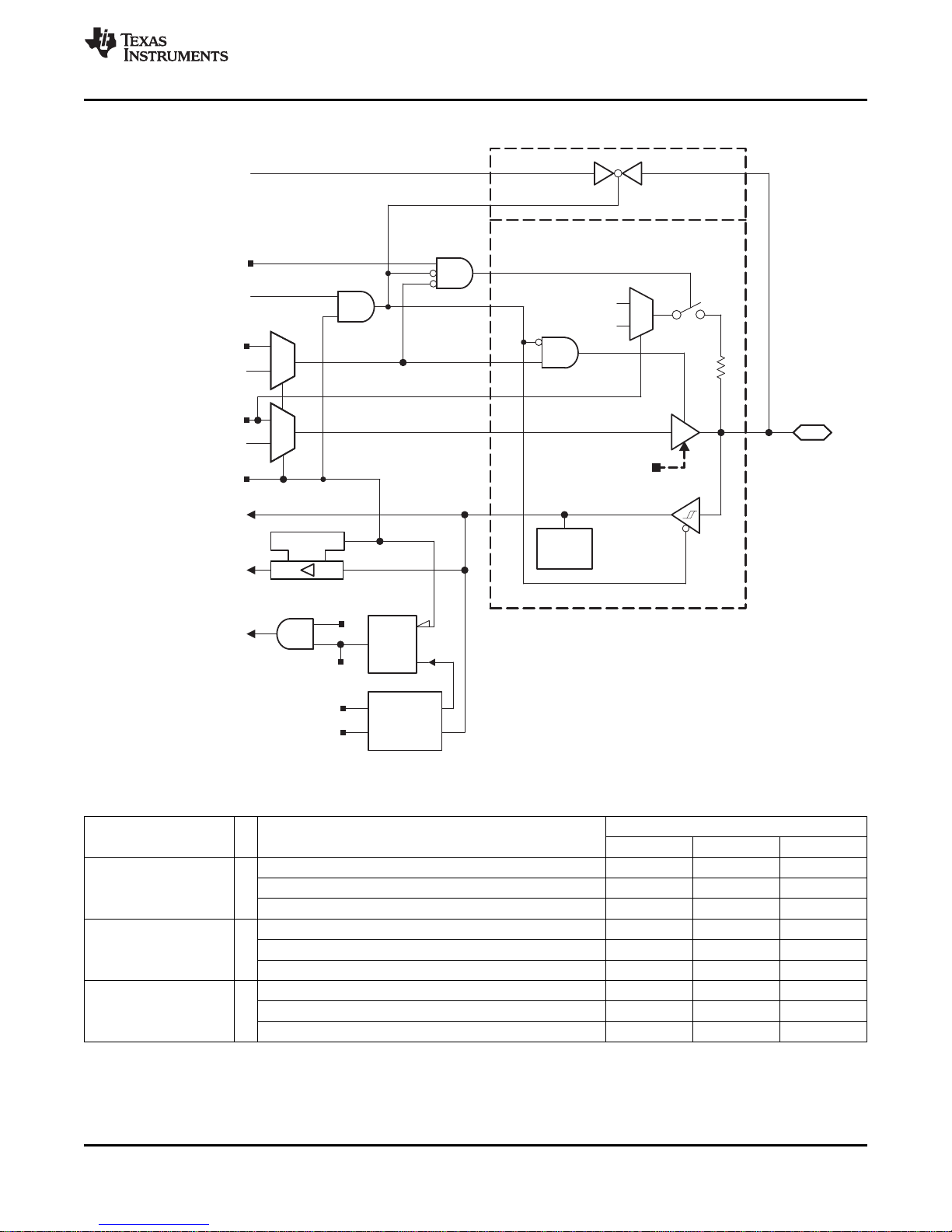
P1.5/P1MAP5(/R23)
P1.6/P1MAP6(/R13)
P1.7/P1MAP7(/R03)
P1SEL.x
1
0
P1DIR.x
P1IN.x
P1IRQ.x
EN
to Port Mapping
1
0
from Port Mapping
P1OUT.x
Interrupt
Edge
Select
Q
EN
Set
P1SEL.x
P1IES.x
P1IFG.x
P1IE.x
1
0
DVSS
DVCC
1
P1DS.x
0: Low drive
1: High drive
D
from Port Mapping
to LCD_B
Pad Logic
Bus
Keeper
Direction
0: Input
1: Output
P1REN.x
P1MAP.x = PMAP_ANALOG
(n/a CC430F513x)
ECCN 5E002 TSPA - Technology / Software Publicly Available
CC430F6137, CC430F6135, CC430F6127, CC430F6126, CC430F6125
www.ti.com
Port P1, P1.5 to P1.7, Input/Output With Schmitt Trigger
CC430F5137, CC430F5135, CC430F5133
SLAS554H –MAY 2009–REVISED SEPTEMBER 2013
CC430F513x devices don't provide LCD functionality on port P1 pins.
Table 50. Port P1 (P1.5 to P1.7) Pin Functions
PIN NAME (P1.x) x FUNCTION
P1.5/P1MAP5/R23 5 P1.5 (I/O) I: 0; O: 1 0 X
P1.6/P1MAP6/R13/ 6 P1.6 (I/O) I: 0; O: 1 0 X
LCDREF
P1.7/P1MAP7/R03 7 P1.7 (I/O) I: 0; O: 1 0 X
(1) X = don't care
(2) According to mapped function - see Table 9.
(3) Setting P1SEL.x bit together with P1MAPx = PM_ANALOG disables the output driver as well as the input Schmitt trigger.
Copyright © 2009–2013, Texas Instruments Incorporated Submit Documentation Feedback 91
Mapped secondary digital function - see Table 9 0; 1
(3)
R23
(not available on CC430F513x) X 1 = 31
Mapped secondary digital function - see Table 9 0; 1
R13/LCDREF
Mapped secondary digital function - see Table 9 0; 1
(3)
R03
(not available on CC430F513x) X 1 = 31
Product Folder Links: CC430F6137 CC430F6135 CC430F6127 CC430F6126 CC430F6125 CC430F5137
CONTROL BITS/SIGNALS
P1DIR.x P1SEL.x P1MAPx
(2)
(3)
(not available on CC430F513x) X 1 = 31
(2)
(2)
1 ≤ 30
1 ≤ 30
1 ≤ 30
CC430F5135 CC430F5133
(1)
(2)
(2)
(2)
Page 92

P2.0/P2MAP0/CB0(/A0)
P2.1/P2MAP2/CB1(/A1)
P2.2/P2MAP2/CB2(/A2)
P2.3/P2MAP3/CB3(/A3)
Direction
0:Input
1:Output
P2SEL.x
1
0
P2DIR.x
P2IN.x
P2IRQ.x
EN
toPortMapping
1
0
fromPortMapping
P2OUT.x
Interrupt
Select
Edge
Q
EN
Set
P2 .SEL x
P2IESx.
P2IFG.x
P2IE.x
1
0
DVSS
DVCC
1
P2DS.x
0:Lowdrive
1:Highdrive
D
fromPortMapping
ToComparator_B
fromComparator_B
PadLogic
ToADC12
INCHx=x
(n/aCC430F612x)
CBPD.x
P2REN.x
P2MAP.x=PMAP_ANALOG
Bus
Keeper
ECCN 5E002 TSPA - Technology / Software Publicly Available
CC430F6137, CC430F6135, CC430F6127, CC430F6126, CC430F6125
CC430F5137, CC430F5135, CC430F5133
SLAS554H –MAY 2009–REVISED SEPTEMBER 2013
Port P2, P2.0 to P2.3, Input/Output With Schmitt Trigger
www.ti.com
92 Submit Documentation Feedback Copyright © 2009–2013, Texas Instruments Incorporated
Product Folder Links: CC430F6137 CC430F6135 CC430F6127 CC430F6126 CC430F6125 CC430F5137
CC430F5135 CC430F5133
Page 93
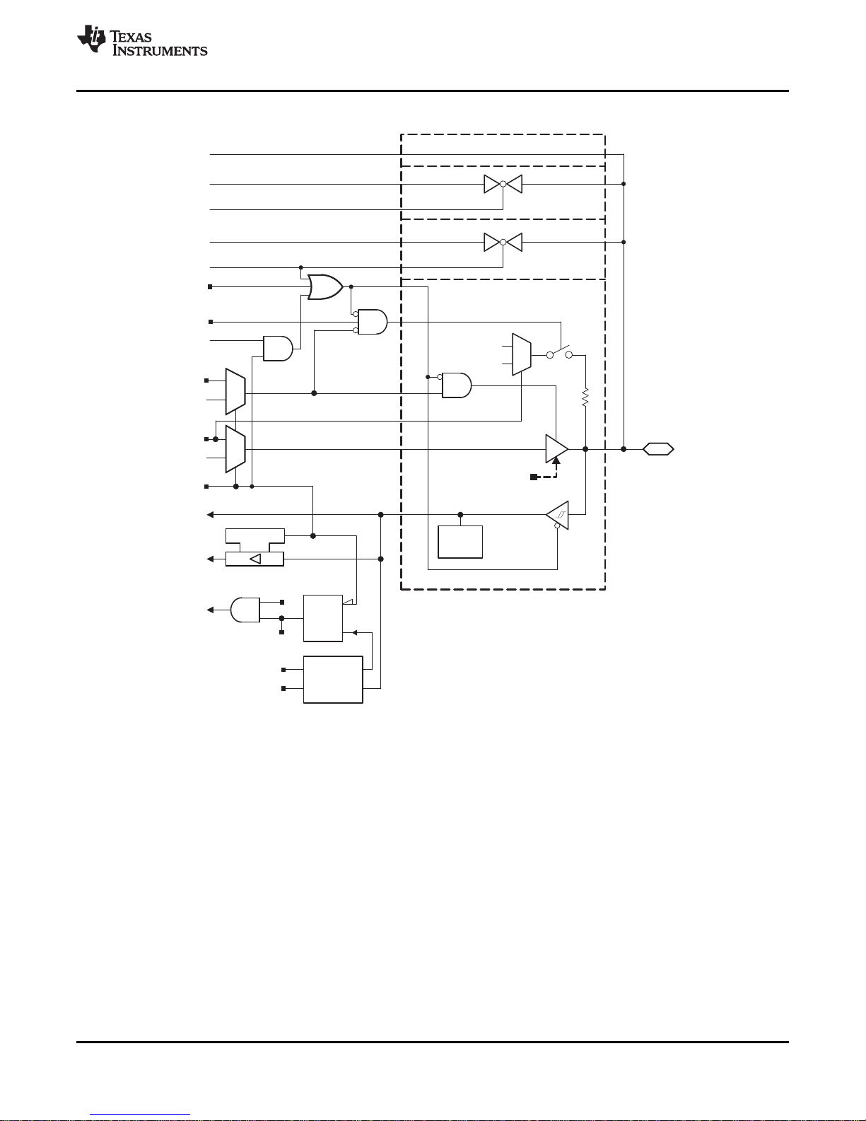
P2.4/P2MAP4/CB4(/A4/VREF-/VeREF-)
P2.5/P2MAP5/CB5(/A5/VREF+/VeRF+)
P2SEL.x
1
0
P2DIR.x
P2IN.x
P2IRQ.x
EN
toPortMapping
1
0
fromPortMapping
P2OUT.x
Interrupt
Select
Edge
Q
EN
Set
P2 .SEL x
P2IESx.
P2IFG.x
P2IE.x
1
0
DVSS
DVCC
1
P2DS.x
0:Lowdrive
1:Highdrive
D
fromPortMapping
ToComparator_B
fromComparator_B
PadLogic
ToADC12
INCHx=x
(n/aCC430F612x)
Bus
Keeper
to/fromReference
(n/aCC430F612x)
Direction
0:Input
1:Output
CBPD.x
P2REN.x
P2MAP.x=PMAP_ANALOG
ECCN 5E002 TSPA - Technology / Software Publicly Available
CC430F6137, CC430F6135, CC430F6127, CC430F6126, CC430F6125
www.ti.com
Port P2, P2.4 to P2.5, Input/Output With Schmitt Trigger
CC430F5137, CC430F5135, CC430F5133
SLAS554H –MAY 2009–REVISED SEPTEMBER 2013
Copyright © 2009–2013, Texas Instruments Incorporated Submit Documentation Feedback 93
Product Folder Links: CC430F6137 CC430F6135 CC430F6127 CC430F6126 CC430F6125 CC430F5137
CC430F5135 CC430F5133
Page 94
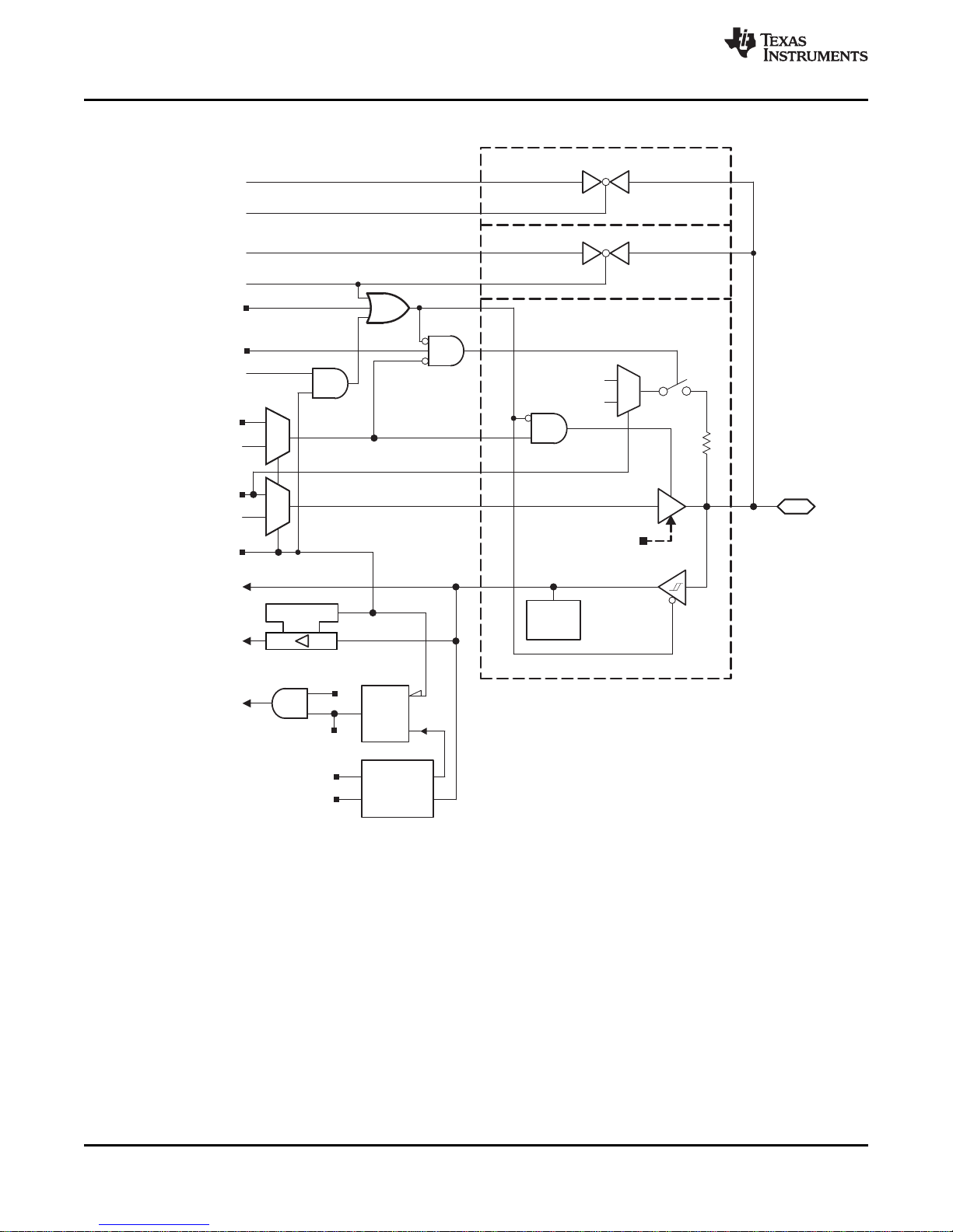
P2.6/P2MAP6(/CB6/A6)
P2.7/P2MAP7(/CB7/A7)
Direction
0:Input
1:Output
P2SEL.x
1
0
P2DIR.x
P2IN.x
P2IRQ.x
EN
toPortMapping
1
0
fromPortMapping
P2OUT.x
Interrupt
Select
Edge
Q
EN
Set
P2 .SEL x
P2IESx.
P2IFG.x
P2IE.x
1
0
DVSS
DVCC
1
P2DS.x
0:Lowdrive
1:Highdrive
D
fromPortMapping
ToComparator_B
fromComparator_B
PadLogic
ToADC12
INCHx=x
(n/aCC430F513x)
(n/aCC430F513x)
(n/aCC430F513x)
CBPD.x
P2REN.x
P2MAP.x=PMAP_ANALOG
Bus
Keeper
ECCN 5E002 TSPA - Technology / Software Publicly Available
CC430F6137, CC430F6135, CC430F6127, CC430F6126, CC430F6125
CC430F5137, CC430F5135, CC430F5133
SLAS554H –MAY 2009–REVISED SEPTEMBER 2013
Port P2, P2.6 and P2.7, Input/Output With Schmitt Trigger
www.ti.com
CC430F513x devices don't provide analog functionality on port P2.6 and P2.7 pins.
94 Submit Documentation Feedback Copyright © 2009–2013, Texas Instruments Incorporated
Product Folder Links: CC430F6137 CC430F6135 CC430F6127 CC430F6126 CC430F6125 CC430F5137
CC430F5135 CC430F5133
Page 95
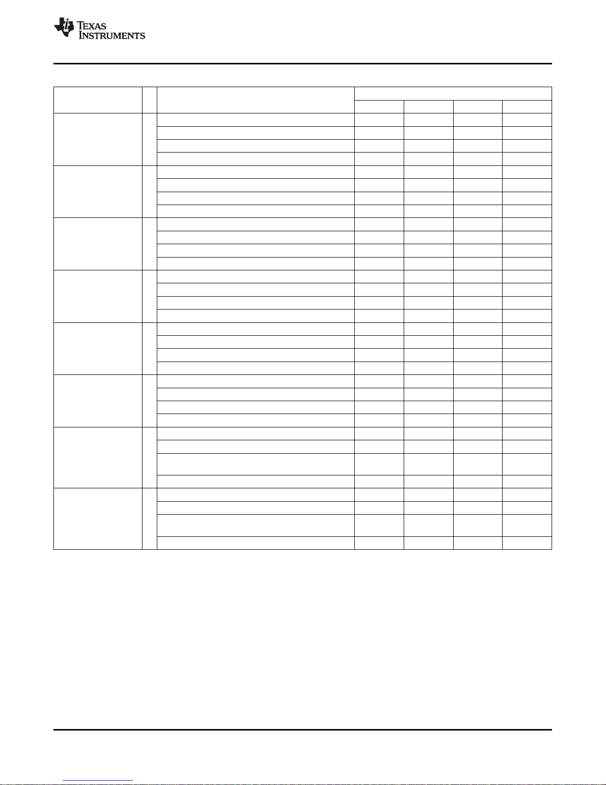
ECCN 5E002 TSPA - Technology / Software Publicly Available
CC430F6137, CC430F6135, CC430F6127, CC430F6126, CC430F6125
CC430F5137, CC430F5135, CC430F5133
www.ti.com
Table 51. Port P2 (P2.0 to P2.7) Pin Functions
PIN NAME (P2.x) x FUNCTION
P2.0/P2MAP0/CB0 0 P2.0 (I/O) I: 0; O: 1 0 X 0
(/A0)
P2.1/P2MAP1/CB1 1 P2.1 (I/O) I: 0; O: 1 0 X 0
(/A1)
P2.2/P2MAP2/CB2 2 P2.2 (I/O) I: 0; O: 1 0 X 0
(/A2)
P2.3/P2MAP3/CB3 3 P2.3 (I/O) I: 0; O: 1 0 X 0
(/A3)
P2.4/P2MAP4/CB4 4 P2.4 (I/O) I: 0; O: 1 0 X 0
(/A4/VREF-/VeREF-)
P2.5/P2MAP5/CB5 5 P2.5 (I/O) I: 0; O: 1 0 X 0
(/A5/VREF+/VeREF+)
P2.6/P2MAP6(/CB6) 6 P2.6 (I/O) I: 0; O: 1 0 X 0
(/A6)
P2.7/P2MAP7(/CB7) 7 P2.7 (I/O) I: 0; O: 1 0 X 0
(/A7)
(1) X = don't care
(2) According to mapped function - see Table 9.
(3) Setting P2SEL.x bit together with P2MAPx = PM_ANALOG disables the output driver as well as the input Schmitt trigger.
(4) Setting the CBPD.x bit disables the output driver as well as the input Schmitt trigger to prevent parasitic cross currents when applying
analog signals. Selecting the CBx input pin to the comparator multiplexer with the CBx bits automatically disables output driver and input
buffer for that pin, regardless of the state of the associated CBPD.x bit.
Mapped secondary digital function - see Table 9 0; 1
A0 (not available on CC430F612x)
(4)
CB0
(3)
Mapped secondary digital function - see Table 9 0; 1
A1 (not available on CC430F612x)
(4)
CB1
(3)
Mapped secondary digital function - see Table 9 0; 1
A2 (not available on CC430F612x)
(4)
CB2
(3)
Mapped secondary digital function - see Table 9 0; 1
A3 (not available on CC430F612x)
(4)
CB3
(3)
Mapped secondary digital function - see Table 9 0; 1
A4/VREF-/VeREF- (not available on CC430F612x)
(4)
CB4
(3)
Mapped secondary digital function - see Table 9 0; 1
A5/VREF+/VeREF+ (not available on CC430F612x)
(4)
CB5
(3)
Mapped secondary digital function - see Table 9 0; 1
A6 (not available on CC430F612x and
CC430F513x)
CB6 (not available on CC430F513x)
(3)
(4)
Mapped secondary digital function - see Table 9 0; 1
A7 (not available on CC430F612x and
CC430F513x)
CB7 (not available on CC430F513x)
(3)
(4)
SLAS554H –MAY 2009–REVISED SEPTEMBER 2013
CONTROL BITS/SIGNALS
(1)
P2DIR.x P2SEL.x P2MAPx CBPD.x
(2)
1 ≤ 30
(2)
0
X 1 = 31 X
X X X 1
(2)
1 ≤ 30
(2)
0
X 1 = 31 X
X X X 1
(2)
1 ≤ 30
(2)
0
X 1 = 31 X
X X X 1
(2)
1 ≤ 30
(2)
0
X 1 = 31 X
X X X 1
(2)
1 ≤ 30
(2)
0
X 1 = 31 X
X X X 1
(2)
1 ≤ 30
(2)
0
X 1 = 31 X
X X X 1
(2)
1 ≤ 30
(2)
0
X 1 = 31 X
X X X 1
(2)
1 ≤ 30
(2)
0
X 1 = 31 X
X X X 1
Copyright © 2009–2013, Texas Instruments Incorporated Submit Documentation Feedback 95
Product Folder Links: CC430F6137 CC430F6135 CC430F6127 CC430F6126 CC430F6125 CC430F5137
CC430F5135 CC430F5133
Page 96

P3.4/P3MAP4(/S14)
P3.5/P3MAP5(/S15)
P3.6/P3MAP6(/S16)
P3.7/P3MAP7(/S17)
P3.0/P3MAP0(/S10)
P3.1/P3MAP1(/S11)
P3.2/P3MAP2(/S12)
P3.3/P3MAP3(/S13)
Direction
0:Input
1:Output
P3SEL.x
1
0
P3DIR.x
P3IN.x
EN
toPortMapping
1
0
fromPortMapping
P3OUT.x
1
0
DVSS
DVCC
1
P3DS.x
0:Lowdrive
1:Highdrive
D
fromPortMapping
S10...S17
LCDS10...LCDS17
PadLogic
P3REN.x
P3MAP.x=PMAP_ANALOG
Bus
Keeper
(n/aCC430F513x)
ECCN 5E002 TSPA - Technology / Software Publicly Available
CC430F6137, CC430F6135, CC430F6127, CC430F6126, CC430F6125
CC430F5137, CC430F5135, CC430F5133
SLAS554H –MAY 2009–REVISED SEPTEMBER 2013
Port P3, P3.0 to P3.7, Input/Output With Schmitt Trigger
www.ti.com
CC430F513x devices don't provide LCD functionality on port P3 pins.
96 Submit Documentation Feedback Copyright © 2009–2013, Texas Instruments Incorporated
Product Folder Links: CC430F6137 CC430F6135 CC430F6127 CC430F6126 CC430F6125 CC430F5137
CC430F5135 CC430F5133
Page 97

ECCN 5E002 TSPA - Technology / Software Publicly Available
CC430F6137, CC430F6135, CC430F6127, CC430F6126, CC430F6125
CC430F5137, CC430F5135, CC430F5133
www.ti.com
Table 52. Port P3 (P3.0 to P3.7) Pin Functions
PIN NAME (P3.x) x FUNCTION
P3.0/P3MAP0/S10 0 P3.0 (I/O) I: 0; O: 1 0 X 0
Mapped secondary digital function - see Table 9 0; 1
Output driver and input Schmitt trigger disabled X 1 = 31 0
S10 (not available on CC430F513x) X X X 1
P3.1/P3MAP1/S11 1 P3.1 (I/O) I: 0; O: 1 0 X 0
Mapped secondary digital function - see Table 9 0; 1
Output driver and input Schmitt trigger disabled X 1 = 31 0
S11 (not available on CC430F513x) X X X 1
P3.2/P3MAP7/S12 2 P3.2 (I/O) I: 0; O: 1 0 X 0
Mapped secondary digital function - see Table 9 0; 1
Output driver and input Schmitt trigger disabled X 1 = 31 0
S12 (not available on CC430F513x) X X X 1
P3.3/P3MAP3/S13 3 P3.3 (I/O) I: 0; O: 1 0 X 0
Mapped secondary digital function - see Table 9 0; 1
Output driver and input Schmitt trigger disabled X 1 = 31 0
S13 (not available on CC430F513x) X X X 1
P3.4/P3MAP4/S14 4 P3.4 (I/O) I: 0; O: 1 0 X 0
Mapped secondary digital function - see Table 9 0; 1
Output driver and input Schmitt trigger disabled X 1 = 31 0
S14 (not available on CC430F513x) X X X 1
P3.5/P3MAP5/S15 5 P3.5 (I/O) I: 0; O: 1 0 X 0
Mapped secondary digital function - see Table 9 0; 1
Output driver and input Schmitt trigger disabled X 1 = 31 0
S15 (not available on CC430F513x) X X X 1
P3.6/P3MAP6/S16 6 P3.6 (I/O) I: 0; O: 1 0 X 0
Mapped secondary digital function - see Table 9 0; 1
Output driver and input Schmitt trigger disabled X 1 = 31 0
S16 (not available on CC430F513x) X X X 1
P3.7/P3MAP7/S17 7 P3.7 (I/O) I: 0; O: 1 0 X 0
Mapped secondary digital function - see Table 9 0; 1
Output driver and input Schmitt trigger disabled X 1 = 31 0
S17 (not available on CC430F513x) X X X 1
(1) X = don't care
(2) LCDSx not available in CC430F513x.
(3) According to mapped function - see Table 9.
SLAS554H –MAY 2009–REVISED SEPTEMBER 2013
CONTROL BITS/SIGNALS
P3DIR.x P3SEL.x P3MAPx
(3)
(3)
(3)
(3)
(3)
(3)
(3)
(3)
1 ≤ 30
1 ≤ 30
1 ≤ 30
1 ≤ 30
1 ≤ 30
1 ≤ 30
1 ≤ 30
1 ≤ 30
(1)
LCDS10...
(3)
(3)
(3)
(3)
(3)
(3)
(3)
(3)
17
(2)
0
0
0
0
0
0
0
0
Copyright © 2009–2013, Texas Instruments Incorporated Submit Documentation Feedback 97
Product Folder Links: CC430F6137 CC430F6135 CC430F6127 CC430F6126 CC430F6125 CC430F5137
CC430F5135 CC430F5133
Page 98

P4.4/S6
P4.5/S7
P4.6/S8
P4.7/S9
P4.0/S2
P4.1/S3
P4.2/S4
P4.3/S5
Direction
0:Input
1:Output
P4SEL.x
1
0
P4DIR.x
P4IN.x
EN
NotUsed
1
0
DVSS
P4OUT.x
1
0
DVSS
DVCC
1
P4DS.x
0:Lowdrive
1:Highdrive
D
S2...S9
LCDS2...LCDS9
PadLogic
P4REN.x
Bus
Keeper
ECCN 5E002 TSPA - Technology / Software Publicly Available
CC430F6137, CC430F6135, CC430F6127, CC430F6126, CC430F6125
CC430F5137, CC430F5135, CC430F5133
SLAS554H –MAY 2009–REVISED SEPTEMBER 2013
Port P4, P4.0 to P4.7, Input/Output With Schmitt Trigger (CC430F613x and CC430F612x only)
www.ti.com
98 Submit Documentation Feedback Copyright © 2009–2013, Texas Instruments Incorporated
Product Folder Links: CC430F6137 CC430F6135 CC430F6127 CC430F6126 CC430F6125 CC430F5137
CC430F5135 CC430F5133
Page 99

ECCN 5E002 TSPA - Technology / Software Publicly Available
CC430F6137, CC430F6135, CC430F6127, CC430F6126, CC430F6125
CC430F5137, CC430F5135, CC430F5133
www.ti.com
Table 53. Port P4 (P4.0 to P4.7) Pin Functions (CC430F613x and CC430F612x only)
PIN NAME (P4.x) x FUNCTION
P4.0/P4MAP0/S2 0 P4.0 (I/O) I: 0; O: 1 0 0
N/A 0 1 0
DVSS 1 1 0
S2 X X 1
P4.1/P4MAP1/S3 1 P4.1 (I/O) I: 0; O: 1 0 0
N/A 0 1 0
DVSS 1 1 0
S3 X X 1
P4.2/P4MAP7/S4 2 P4.2 (I/O) I: 0; O: 1 0 0
N/A 0 1 0
DVSS 1 1 0
S4 X X 1
P4.3/P4MAP3/S5 3 P4.3 (I/O) I: 0; O: 1 0 0
N/A 0 1 0
DVSS 1 1 0
S5 X X 1
P4.4/P4MAP4/S6 4 P4.4 (I/O) I: 0; O: 1 0 0
N/A 0 1 0
DVSS 1 1 0
S6 X X 1
P4.5/P4MAP5/S7 5 P4.5 (I/O) I: 0; O: 1 0 0
N/A 0 1 0
DVSS 1 1 0
S7 X X 1
P4.6/P4MAP6/S8 6 P4.6 (I/O) I: 0; O: 1 0 0
N/A 0 1 0
DVSS 1 1 0
S8 X X 1
P4.7/P4MAP7/S9 7 P4.7 (I/O) I: 0; O: 1 0 0
N/A 0 1 0
DVSS 1 1 0
S9 X X 1
(1) X = don't care
SLAS554H –MAY 2009–REVISED SEPTEMBER 2013
CONTROL BITS/SIGNALS
P4DIR.x P4SEL.x LCDS2...7
(1)
Copyright © 2009–2013, Texas Instruments Incorporated Submit Documentation Feedback 99
Product Folder Links: CC430F6137 CC430F6135 CC430F6127 CC430F6126 CC430F6125 CC430F5137
CC430F5135 CC430F5133
Page 100
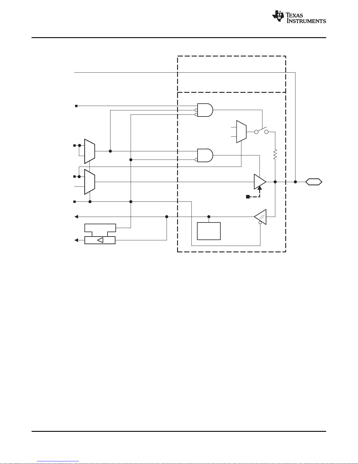
P5.0/XIN
P5SEL.0
1
0
P5DIR.0
P5IN.0
EN
ModuleXIN
1
0
ModuleXOUT
P5OUT.0
1
0
DVSS
DVCC
P5REN.0
PadLogic
1
P5DS.x
0:Lowdrive
1:Highdrive
D
Bus
Keeper
toXT1
ECCN 5E002 TSPA - Technology / Software Publicly Available
CC430F6137, CC430F6135, CC430F6127, CC430F6126, CC430F6125
CC430F5137, CC430F5135, CC430F5133
SLAS554H –MAY 2009–REVISED SEPTEMBER 2013
Port P5, P5.0, Input/Output With Schmitt Trigger
www.ti.com
100 Submit Documentation Feedback Copyright © 2009–2013, Texas Instruments Incorporated
Product Folder Links: CC430F6137 CC430F6135 CC430F6127 CC430F6126 CC430F6125 CC430F5137
CC430F5135 CC430F5133
 Loading...