

Page 1

User Manual
Rev. 1.5
CC400DK Development Kit
Page 2

CC400DK Development kit (rev. 1.5) 2002-09-17 Page 2 of 22
Table of contents
TABLE OF CONTENTS............................................................................................................ 2
INTRODUCTION ....................................................................................................................... 3
EVALUATION BOARD............................................................................................................. 3
DESCRIPTION ........................................................................................................................... 4
LAYOUT SKETCHES AND CIRCUIT DRAWINGS............................................................................... 9
BILL OF MATERIALS................................................................................................................. 15
USING THE DEVELOPMENT KIT.......................................................................................... 19
APPENDIX A........................................................................................................................... 20
A.1 FINE TUNING PROCEDURE OF LNA/PA MATCHING NETWORK.......................................... 20
Page 3

CC400DK Development kit (rev. 1.5) 2002-09-17 Page 3 of 22
Introduction
The CC400 single chip transceiver includes many features and great flexibility which makes
the chip suitable for a very large number of applications and system requirements. The
CC400 Development Kit is designed to make it very easy for the user to evaluate transceiver
performance and in short time develop his own applications.
The Development Kit includes two evaluation boards with a complete CC400 transceiver,
voltage regulator and PC interface circuitry. Using the evaluation board connected to a PC
running the SmartRF
®
Studio software, various system parameters can be changed and
tested by key-strokes.
Technical features:
RF power up to 25mW (14dBm) programmable in 1dB steps
-112 dBm sensitivity for 10
-3
bit error rate (1.2kbps, 20kHz frequency separation)
Logic level data input/output (Manchester coded)
Selectable RF filtering (SAW or LC)
Selectable IF filtering
All set-up controlled by PC
Selectable 3V or 4-10Vunregulated voltage supply inputs
This user manual describes how to get started with the Development Kit. You will also find
detailed description of the evaluation board and advice how to develop your own applications.
For details on how to use the SmartRF
®
Studio software please refer to the SmartRF® Studio
user manual.
Your SmartRF
®
CC400DK Development Kit should contain the following items:
Evaluation circuit boards (PCB) 2 ex
CC400 single chip transceiver 5 ex
PC parallel port extension cable 2 ex 25-pin D-sub, male-female, 3m
Adapter 4 ex SMA male-BNC female
Antenna 2 ex 50Ω, λ/4 monopole, SMA male
Quick Start Instructions
SmartRF
®
CD-ROM
The evaluation board includes a significant number of components for great flexibility.
However, only a minor part of these components are required in an actual application. Check
the datasheet for a typical application circuitry.
Evaluation board
Page 4

CC400DK Development kit (rev. 1.5) 2002-09-17 Page 4 of 22
The kit includes an evaluation circuit board (PCB) with the following items:
• CC400
• Necessary external surface mounted devices, SMD, for the chip.
• Voltage regulator 4V-10V to 3V regulated voltage.
• Possibilities to apply a 3V voltage source directly (chosen by switches or connectors
at the board).
• Voltage-level interface circuits between the CC400 (3V) and the parallel port of the
computer (5V).
• Connector for a PC parallel port cable.
• Connector for antenna and modulation data in/out.
• Edge connector for future use.
This board is designed with great flexibility so that you can evaluate the circuit performance
for several circuit configurations, and in development of your own applications. A layout
sketch of the evaluation board is shown in chapter 0.
Description
The evaluation circuit board constitutes of three main parts. These are the RF-section, the
voltage supply and the PC-interface. The PC-interface contains voltage level shift circuit,
which buffers the control lines.
Voltage supply
You can chose between applying a 4-10V non-regulated supply voltage or a 3V regulated
supply voltage by setting a switch on the board (SPDT). If a non-regulated supply voltage is
applied, an on board regulator generates a regulated 3V supply. A diode prevents damage if
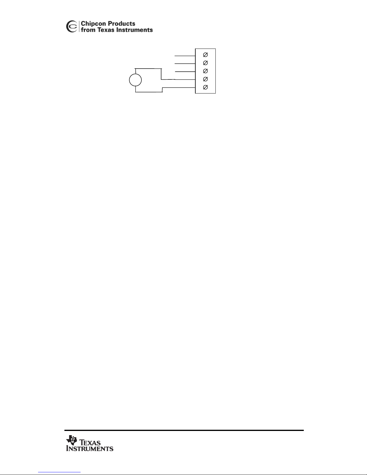
wrong polarity is used for the non-regulated input. The connector has five contacts, which is
shown below. In addition to the three supply voltage contacts, there are two contacts, which
can be used to measure the DC current to the CC400 chip. A short jumper is placed between
these two contacts for the circuit to work. If you want to measure the DC current, replace the
jumper with an amperemeter (as shown in the figure below). The current range is from 0 to 70
mA.
Page 5
CC400DK Development kit (rev. 1.5) 2002-09-17 Page 5 of 22
Figure: The power connector with an amperemeter attached.
RF-section
The RF section consists of a CC400 chip with external components. The different
components are explained below.
The loop filter
The PLL loop filter contains the components C121-C123 and R121-R123. The software
program calculates the component values. Using the calculated component values for the
loop filter will give an optimum loop bandwidth for the selected system parameters.
The component values used in the CC400EB is selected for 9.6 kbit/s data rate, but can also
be used for evaluation of lower data rates.
The transmitted frequency is FSK modulated, which means that the bits ‘0’ and ‘1’ has
different frequencies, see Frequency separation in chapter 4.1.1.5 in SmartRF
®
Studio user
manual.
Note: If you need a shorter switching time between the two frequencies, the PLL settling time
has to be shorter. To find the new component values that you need for the loop filter, the
software program can be used as a calculator. Using a higher data rate value will give you a
larger loop bandwidth, but also an increase in the side-band noise on the carrier. A warning
may appear when increasing the data rate. To get around this warning, try to set the X-tal
accuracy to zero. Do not update the device when doing this, but use Enter to calculate the
values and return to your earlier settings afterwards.
External IF filter
The evaluation board is equipped with an external 455kHz ceramic filter. Input and output
impedance to the CC400 is 1.5kΩ, and the bandwidth is approximately 30kHz.
4-10V
0V
3V
I
out
A
Page 6
CC400DK Development kit (rev. 1.5) 2002-09-17 Page 6 of 22
The LOCK signal
A LOCK signal is connected to the parallel port interface to be monitored by the software. The
signal tells you if the synthesiser frequency is in lock. It is also available at a test pin, TP2,
and is active high.
NOTE: If Power Down mode is selected when the LOCK signal is high, the current
consumption will be approximately 23 uA. This is due to the current flowing from the LOCK
pin into the external buffer transistor (Q2). This transistor could be replaced with a MOSFET
to avoid this trickle current. Without this extra load the CC400 Power Down current is less
than 1 uA.
The modulation input/output
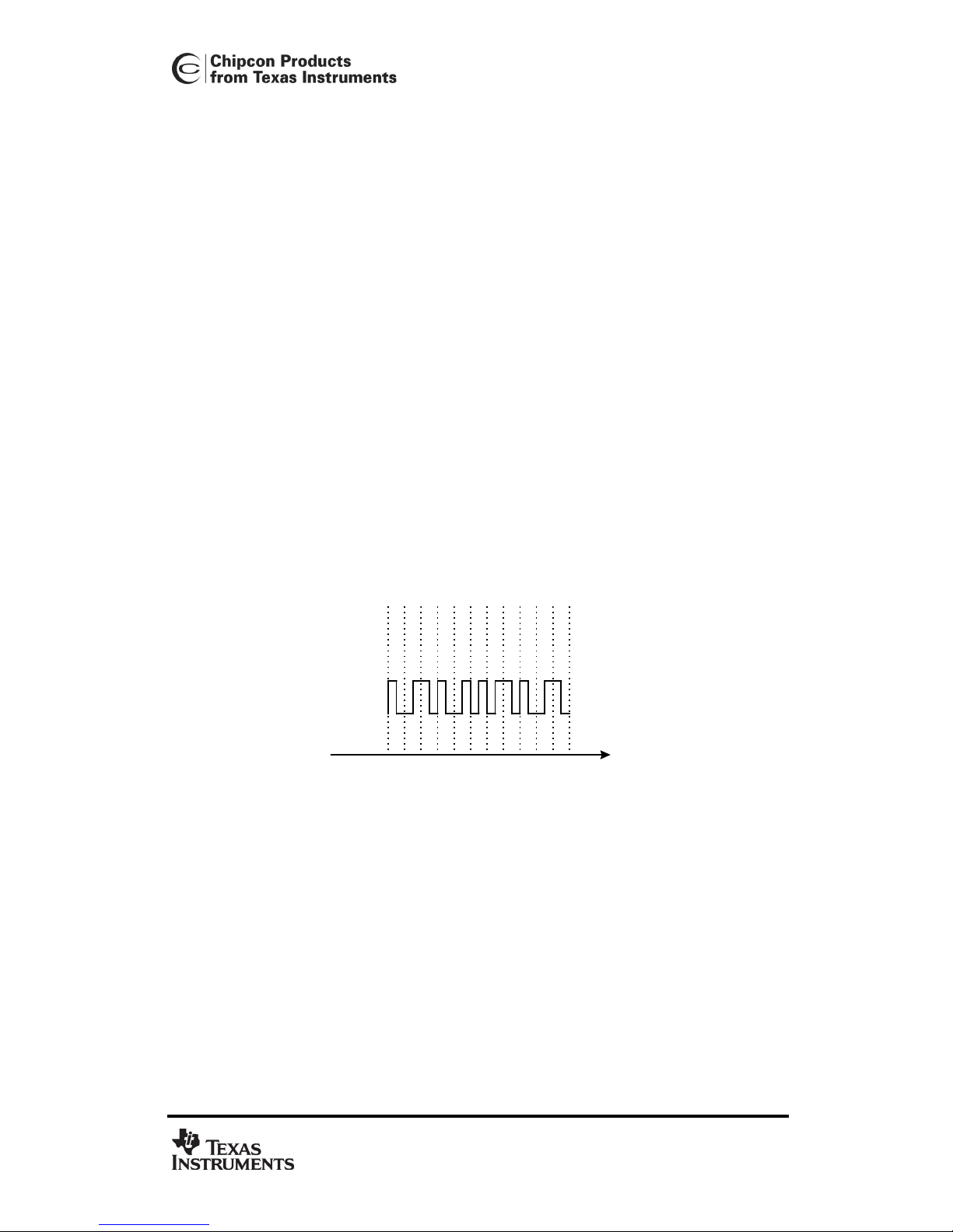
The modulation input/output (DIO) is connected to a separate connector. The connector type
is SMA female. The data to be sent has to be Manchester encoded (also known as bi-phaselevel coding). The Manchester code ensures that the signal has no DC component, which is
necessary for the FSK demodulator. The Manchester code is based on transitions; a “0” is
encoded as a low-to-high transition, a “1” is encoded as a high-to-low transition. See figure
below. Maximum data-rate is 9.6 kbit/s and is chosen in the software. To test your module
use a 3V
pp
logic level with 1-10 kHz square wave.
Time
TX
data
1 0 1 1 0 0 0 1 1 0 1
LNA/PA matching
The input/output matching network is optimised for 433.92MHz operation. The component
values are calculated in the software program, and consist of C51, C61, L51 and L61. Using
the specified component values for the input/output match will give an optimum match at the
specified operating frequency. Minor tuning of the component values may be necessary to
compensate for layout parasitics at other frequencies or other layouts. See appendix A.
Page 7

CC400DK Development kit (rev. 1.5) 2002-09-17 Page 7 of 22
The Voltage Controlled Oscillator (VCO)
The VCO tank on the evaluation board is optimised for the 433MHz band, covering
approximately 410 – 450MHz. The tank contains the components C91, C92, C93, L91 and
the variable capacitance D2.
To operate in other frequency bands, C93 and L91 can be altered. To increase the operation
frequency C93 or L91 (or both) should be decreased (use 8.2nH for L91, and 1.5pF or 1.8pF
for C93). To decrease the operation frequency C93 or L91 (or both) should be increased (use
12nH for L91, and 2.7pF or 3.3pF for C93).
To find the tuning range for the new VCO tank, set the RF frequency to 300 MHz and 500
MHz in the software, update the device and measure the output frequency. In this way the
VCO tank will be tuned to its minimum and maximum operation frequency respectively.
For further details, please contact Chipcon.
The crystal oscillator
Crystal frequency is set to 12.000 MHz, X1. The crystal oscillator circuit has a trimmer
capacitor, CT152, which reduces the initial tolerance of the crystal to zero by careful
adjustment using a precision frequency counter. The crystal used at this board has ±10 ppm
initial tolerance and ±10 ppm drift over the –10 to +70 °C temperature range. The crystal
oscillator has an AC coupled (C153) test pin for external clock injection, TP1. Be sure to
remove the crystal when an external clock is used. The external clock should have amplitude
of 1-3V
pp
. If using other crystals they should be designed for 12pF load capacitance.
The preselector filter options
There are three preselector filter options: LC-filter, SAW filter, or no filter used. Each of the
three filter alternatives is equipped with a female SMA antenna connector. To choose
between the three filters there is a zero ohm resistor that can be moved (R61-R63).
Page 8

CC400DK Development kit (rev. 1.5) 2002-09-17 Page 8 of 22
Unfiltered antenna output
The unfiltered antenna output has been made with an option. Two components, L71 and
C71, can be used to match the antenna if the antenna impedance is different from 50Ω. To
select this output the zero ohm resistor must be put in R61, and R62 and R63 shall not be
mounted.
LC-filtered antenna output
A LC-filter consisting of L52, C52 and C53 make up a 3dB-equal ripple low-pass filter that
prevents harmonics to be emitted from the transmitter. In receive mode the filter removes
high frequencies in order to prevent distortion and jamming of in the receiver. The filter is
designed for 50Ω termination impedance. The LC-filter is selected by placing the zero ohm
resistor in the R62 position. For operation at other frequencies, please use the formulas
below.
⎟
⎠
⎞
⎜
⎝
⎛
−⋅≈1333.01
1
RFC
ωω
,
C
L
ω
6.35
=
,
C
C
ω
067.0
=
,
where ω
C
is the cut-off frequency and ωRF is the transmitted RF frequency .
SAW filtered antenna output
To choose this output the zero ohm resistor must be put in the R63 position. The components
around the filter (F2) can be changed to match any SAW filter type. The SAW filter will
introduce additional loss, but will increase the selectivity of the receiver. The 3dB bandwidth
is approximately 200 kHz. The filter can be replaced with another SAW filter with a 3dB
bandwidth of 2 MHz if desirable.
Note: Using the SAW filter, the output power amplifier class should be A or AB and the output
power should not exceed 0 dBm. This will give approximately –5 dBm at the antenna output.
Using power settings above 0 dBm may cause stability problems.
Page 9

CC400DK Development kit (rev. 1.5) 2002-09-17 Page 9 of 22
Layout sketches and circuit drawings
25 pin D-SUB
DIO
ANT
(LC filter)
ANT
(No filter)
ANT
(SAW filter)
4-10V
Switch
Module
slot
(future use)
4-10V
GND
3V
I_out
I_in
3V
Page 10

CC400DK Development kit (rev. 1.5) 2002-09-17 Page 10 of 22
Page 11

CC400DK Development kit (rev. 1.5) 2002-09-17 Page 11 of 22
Page 12

CC400DK Development kit (rev. 1.5) 2002-09-17 Page 12 of 22
Page 13

CC400DK Development kit (rev. 1.5) 2002-09-17 Page 13 of 22
Page 14

CC400DK Development kit (rev. 1.5) 2002-09-17 Page 14 of 22
Page 15

CC400DK Development kit (rev. 1.5) 2002-09-17 Page 15 of 22
Bill of materials
RF part
Reference Description Value Part
C10 Capacitor 0603 1nF C_1N0_0603_NP0_J_50
C11 Capacitor 0805 33nF C_33N_0805_X7R_J_50
C12 Capacitor 1206 4.7nF C_4N7_1206_NP0_J_50
C24 Capacitor 0603 220pF C_220P_0603_NP0_G_50
C25 Capacitor 0603 220pF C_220P_0603_NP0_G_50
C51 Capacitor 0603 220pF C_220P_0603_NP0_G_50
C52 Capacitor 0603 15pF C_15P_0603_NP0_J_50
C53 Capacitor 0603 22pF C_22P_0603_NP0_J_50
C61 Capacitor 0603 15pF C_15P_0603_NP0_G_50
C62 Capacitor 0603 220pF C_220P_0603_NP0_G_50
C63 Capacitor 0805 5.6pF C_5P6_0805_NP0_C_50
C66 Capacitor 0805 Do Not Mount
C68 Capacitor 0805 5.6pF C_5P6_0805_NP0_C_50
C71 Capacitor 0603 Do Not Mount
C91 Capacitor 0603 4.7pF C_4P7_0603_NP0_C_50
C92 Capacitor 0603 8.2pF C_8P2_0603_NP0_C_50
C93 Capacitor 0603 3.9pF C_3P9_0603_NP0_C_50
C121 Capacitor 0603 2.2nF C_2N2_0603_X7R_J_50
C122 Capacitor 0603 120pF C_120P_0603_NP0_J_50
C123 Capacitor 0603 22pF C_22P_0603_NP0_J_50
C151 Capacitor 0603 15pF C_15P_0603_NP0_G_50
C153 Capacitor 0603 1nF C_1N0_0603_NP0_J_50
C161 Capacitor 0603 15pF C_15P_0603_NP0_G_50
C210 Capacitor 0603 1nF C_1N0_0603_NP0_J_50
C211 Capacitor 0805 33nF C_33N_0805_X7R_J_50
C231 Capacitor 0603 Do Not Mount
CT152 Trimmer Capacitor C_3-10P_TRIM_NP0
D2 Varactor diode KV1832C, Toko
F1 Ceramic filter, 455kHz CFUCG455D, Murata
F2 SAW filter, 433.92MHz B3550, Siemens
Page 16

CC400DK Development kit (rev. 1.5) 2002-09-17 Page 16 of 22
L51 Inductor 0805 39nH L_39N_0805_J
L52 Inductor 0805 8.2nH L_8N2_0805_J
L61 Inductor 0805 6.8nH L_6N8_0805_J
L64 Inductor 0805 33nH L_33N_0805_J
L67 Inductor 0805 33nH L_39N_0805_J
L71 Resistor 0805
0Ω
R_0R_0805
L91 Inductor 0805 10nH L_10N_0805_J LQN21A,
Murata
L210 EMI filter bead BLM11A102S, Murata
R24 Resistor 0805 Do Not Mount
R51 Resistor 0805 Do Not Mount
R61 Resistor 0603
0Ω
R_0R_0603
R62 Resistor 0603 Do Not Mount
R63 Resistor 0603 Do Not Mount
R65 Resistor 0805
270Ω
R_270_0805_J
R121 Resistor 0603
27kΩ
R_27K_0603_G
R122 Resistor 0603
150kΩ
R_150K_0603_J
R123 Resistor 0603
22kΩ
R_22K_0603_G
R231 Resistor 0603
0Ω
R_0R_0603
TP1 Testpoint TESTPIN
TP2 Testpoint TESTPIN
U1 Single chip transceiver CC400
X1 Crystal, HC-49-SMD X_12.000000 MHz, 12pF load
Voltage regulator
Reference Description Value Part
C1 Capacitor, tantal
3.3µF
C_3U3_TAN_B
C2 Capacitor, tantal
3.3µF
C_3U3_TAN_B
C3 Capacitor 0805 33nF C_33N_0805_X7R_J_50
D1 Diode, Si BAT254
Q1 MOSFET, P ch. SI9424DY, Siliconix
S1 SPDT switch SWITCH_SPDT
U2 Voltage regulator LP2981, 3V, National
Page 17

CC400DK Development kit (rev. 1.5) 2002-09-17 Page 17 of 22
PC interface
Reference Description Value Part
C26 Capacitor 0805 33nF C_33N_0805_X7R_J_50
C27 Capacitor 0805 33nF C_33N_0805_X7R_J_50
Q2 BJT, Si, NPN, small signal BC846
Q3 BJT, Si, NPN, small signal BC846
Q4 BJT, Si, NPN, small signal BC846
Q5 BJT, Si, NPN, small signal BC846
R1 Resistor 0603
10kΩ
R_10K_0603_G
R2 Resistor 0603
10kΩ
R_10K_0603_G
R3 Resistor 0603
10kΩ
R_10K_0603_G
R4 Resistor 0603
10kΩ
R_10K_0603_G
R5 Resistor 0603
10kΩ
R_10K_0603_G
R6 Resistor 0603
10kΩ
R_10K_0603_G
R7 Resistor 0603
10kΩ
R_10K_0603_G
R8 Resistor 0603
10kΩ
R_10K_0603_G
R9 Resistor 0603
10kΩ
R_10K_0603_G
R10 Resistor 0603
10kΩ
R_10K_0603_G
R11 Resistor 0603
10kΩ
R_10K_0603_G
R12 Resistor 0603
10kΩ
R_10K_0603_G
R13 Resistor 0603
10kΩ
R_10K_0603_G
R14 Resistor 0603
10kΩ
R_10K_0603_G
R15 Resistor 0603
10kΩ
R_10K_0603_G
R16 Resistor 0603
10kΩ
R_10K_0603_G
R17 Resistor 0603
10kΩ
R_10K_0603_G
R18
Resistor 0603
10kΩ
R_10K_0603_G
R19 Resistor 0603
10kΩ
R_10K_0603_G
R20 Resistor 0603
100kΩ
R_100K_0603_G
R21 Resistor 0603
100kΩ
R_100K_0603_G
R22
Resistor 0603
100kΩ
R_100K_0603_G
R23 Resistor 0603
100kΩ
R_100K_0603_G
U3 Hex inverter, oc 74HC05
U4 Hex inverter, oc 74HC05
Page 18

CC400DK Development kit (rev. 1.5) 2002-09-17 Page 18 of 22
Evaluation board
Reference Description Value Part
H1 Circuit Board Support Distance 12.5mm
H2 Circuit Board Support Distance 12.5mm
H3 Circuit Board Support Distance 12.5mm
H4 Circuit Board Support Distance 12.5mm
P1 D-Sub, 25 pin DSUB_25
P2 5 pin terminal, screw SCREW_TERM_5
P3 SMA connector SMA (Straight)
P4 SMA connector SMA (Straight)
P5 SMA connector SMA (Straight)
P6 SMA connector SMA_RA (Right angle)
P8 Edge connector, 2 x 8 pin EDGE_CONN_2X8
Page 19

CC400DK Development kit (rev. 1.5) 2002-09-17 Page 19 of 22
Using the Development Kit
The purpose of the Development Kit is to give users of the integrated transceiver CC400
hands-on experience with the chip. A typical set-up of the evaluation board is shown below.
Each of the evaluation boards is connected to a PC to be programmed by the software.
• How to set up a transmitter.
The data signal that you want to send in transmit mode must be Manchester coded. If you
don’t have Manchester coded signals available, a square wave from a function generator can
be used instead. The signal source shall be connected to the Data I/O port (DIO) at the
evaluation board. The signal must be a square wave from 0 to 3V as shown. Do not apply a
5V signal because it can damage the CC400 chip. The signal from the function generator will
represent either zeroes or ones, and the bit rate will be 1/T, where T is the period time. For
example, when 1.2 kbit/s is used, set the function generator frequency to 1.2 kHz as this will
give a 1.2kbit/s Manchester coded bit stream.
The transmitted signal can be studied on a spectrum analyser, sent out on the antenna (see
note below) or sent to the receiver via a cable with an attenuator attached.
Figure: Equipment set-up in transmit mode.
Antenna
Circuit board
PC
4-10V
Spectrum analyser
DIO
Function generator
3V
T
Page 20

CC400DK Development kit (rev. 1.5) 2002-09-17 Page 20 of 22
• How to set up a receiver
In receive mode a RF generator can be connected to the antenna input to give an ideal RF
signal to the circuit board for testing the receiver. Use FSK modulation with appropriate
deviation and modulation rate. If you don’t have the equipment to send FSK modulation, you
can use a RF generator with FM modulation and use an external function generator to
modulate the signal with a square wave. The RF signal can also come from the transmitter
via the antenna. An oscilloscope is used to see the Manchester coded signal that is being
received.
Figure: Equipment set-up in receive mode.
Important: The use of radio transceivers is regulated by international and national rules.
Before transmitting a RF signal out on the antenna, please contact your local
telecommunication authorities to check if you are licensed to operate the transceiver.
Appendix A
The component values to the input/output matching network are calculated in the software
program, and consist of C51, C61, L51 and L61. Using the specified component values for
the input/output match will give an optimum match at the specified operating frequency. Minor
tuning of the component values may be necessary to compensate for layout parasitics at
other frequencies or other layouts.
A.1 Fine tuning procedure of LNA/PA matching network
Follow the procedure below to fine-tune the matching network. Use the components that the
software program calculates as initial values. Set the bits F5:F3 = 000 in the Register
configuration window and update the device.
1) Receiver tuning
Oscilloscope
Circuit board
PC
4-10V
RF generator
Antenna
DIO
Page 21

CC400DK Development kit (rev. 1.5) 2002-09-17 Page 21 of 22
Connect a Network Analyser to the unfiltered antenna output as shown in the figure, and
measure the impedance at the output.
Figure: Equipment set-up.
Set the CC400 transceiver in RX mode with the software program and adjust L51 and C61
until you measure approximately 50Ω impedance at the antenna output.
2) Transmitter tuning
Connect a Spectrum Analyser to the unfiltered antenna output in the same way as you did for
the RX tuning and measure output power. Set the CC400 transceiver in TX mode and adjust
C61 until you measure the highest output power.
3) Setting the Register bits
Choose the Register configuration window in the software.
1) If the optimum value of C61 found in RX mode is larger than C61 found in TX
mode:
Set bit F2 to 0 and increase bits F5 to F3 by an amount following the formula below
and update the device.
⎟
⎟
⎠
⎞
⎜
⎜
⎝
⎛
−
=
pF
CC
roundFF
TXRX
25.1
6161
3:5
Choose the value of C61 that you got from the TX tuning (C61
TX
).
Circuit board
PC
4-10V
Network analyser
Page 22

CC400DK Development kit (rev. 1.5) 2002-09-17 Page 22 of 22
Example: If C61TX = 12pF and C61RX = 15pF the bits F5:F3 = 010.
2) If the optimum value of C61 found in TX mode is larger than C61 found in RX
mode:
Set bit F2 to 1 and increase bits F5 to F3 by an amount following the formula below
and update the device.
⎟
⎟
⎠
⎞
⎜
⎜
⎝
⎛
−
=
pF
CC
roundFF
RXTX
25.1
6161
3:5
Choose the value of C61 that you got from the RX tuning (C61
RX
).
General Information
Chipcon AS believes the furnished information is correct and accurate at the time of this
printing. However, Chipcon AS reserves the right to make changes to this product without
notice. Chipcon AS does not assume any responsibility for the use of the described product.
Please refer to Chipcon’s web site for the latest update.
SmartRF
®
is a registered trademark of Chipcon AS. SmartRF® is Chipcon's RF technology
platform with RF library cells, modules and design expertise. Based on SmartRF
®
Chipcon
develops standard component RF-circuits as well as full custom ASICs based on customers'
requirements.
 Loading...