

Page 1

CC3235MODSF SimpleLink™ Wi-Fi®and IoT
Solution With MCU LaunchPad™ Hardware
User's Guide
Literature Number: SWRU548
February 2019
Page 2

Contents
1 CC3235MODSF LaunchPad™ Development Kit (LAUNCHCC3235MOD)...................................... 3
1.1 Introduction ................................................................................................................... 5
1.1.1 CC3235MODSF LaunchPad™ ................................................................................... 5
1.1.2 LAUNCHCC3235MOD Key Features ............................................................................ 6
1.1.3 What's Included ..................................................................................................... 6
1.1.4 Regulatory Compliance ........................................................................................... 6
1.1.5 First Steps: Out-of-Box Experience .............................................................................. 7
1.1.6 Next Steps: Looking into the Provided Code ................................................................... 7
1.2 Hardware ..................................................................................................................... 8
1.2.1 Block Diagram....................................................................................................... 9
1.2.2 Hardware Features................................................................................................ 11
1.2.3 BoosterPack Header Pin Assignment ......................................................................... 25
1.2.4 Electrical Characteristics ........................................................................................ 26
1.2.5 Antenna Characteristics ......................................................................................... 26
1.3 Layout Guidelines .......................................................................................................... 27
1.3.1 LAUNCHCC3235MOD Board Layout........................................................................... 27
1.3.2 General Layout Recommendations ............................................................................. 31
1.3.3 RF Layout Recommendations .................................................................................. 31
1.3.4 Antenna Placement and Routing ............................................................................... 33
1.3.5 Transmission Line Considerations ............................................................................. 33
1.4 Operational Setup and Testing .......................................................................................... 35
1.4.1 Measuring the CC3235MOD Current Draw ................................................................... 35
1.4.2 RF Connections ................................................................................................... 36
1.4.3 Design Files ....................................................................................................... 37
1.4.4 Software ........................................................................................................... 37
1.5 Development Environment Requirements .............................................................................. 37
1.5.1 CCS................................................................................................................. 37
1.5.2 IAR .................................................................................................................. 37
1.6 Additional Resources ..................................................................................................... 38
1.6.1 CC3235MODx Product Page ................................................................................... 38
1.6.2 Download CCS, IAR ............................................................................................. 38
1.6.3 SimpleLink™ Academy for CC3235 SDK ..................................................................... 38
1.6.4 TI E2E Community ............................................................................................... 38
1.7 Assembly Drawing and Schematics .................................................................................... 39
1.7.1 Assembly Drawing ................................................................................................ 39
1.7.2 Schematics ........................................................................................................ 40
2
Contents
Copyright © 2019, Texas Instruments Incorporated
SWRU548–February 2019
Submit Documentation Feedback
Page 3

Chapter 1
SWRU548–February 2019
CC3235MODSF LaunchPad™ Development Kit
(LAUNCHCC3235MOD)
Start your design with the industry's first programmable FCC, IC/ISED, ETSI/CE, and MIC Certified
wireless microcontroller (MCU) module with built-in Dual-Band (2.4 GHz and 5 GHz) Wi-Fi®connectivity.
Created for the Internet-of-Things (IoT), the SimpleLink™ CC3235MODx family of devices from Texas
Instruments™ are wireless modules that integrate two physically separated, on-chip MCUs:
• An application processor – ARM®Cortex®-M4 MCU with a user-dedicated 256KB of RAM and an
optional 1MB of Serial Flash.
• A network processor MCU to run all Wi-Fi and Internet logic layers. This ROM based subsystem
includes an 802.11 a/b/g/n radio, baseband, and MAC with a powerful crypto engine for fast, secure
internet connections with 256-bit encryption.
The LAUNCHCC3235MODis a low-cost evaluation platform for MCUs based on ARM Cortex-M4 devices.
The LaunchPad™ design highlights the CC3235MODSF fully-integrated industrial module solution and
Dual-Band Wi-Fi capabilities. The LAUNCHCC3235MOD also features temperature and accelerometer
sensors, programmable user buttons, an RBG LED for custom applications, and onboard emulation for
debugging. The stackable headers interface demonstrates how easy it is to expand the functionality of the
LaunchPad when interfacing with other peripherals on existing BoosterPack™ add-on boards, such as
graphical displays, audio codec, antenna selection, environmental sensing, and more.
Figure 1-1 shows the CC3235MODSF LaunchPad development kit.
SWRU548–February 2019
Submit Documentation Feedback
CC3235MODSF LaunchPad™ Development Kit (LAUNCHCC3235MOD)
Copyright © 2019, Texas Instruments Incorporated
3
Page 4
www.ti.com
Figure 1-1. CC3235MODSF SimpleLinkTMWi-Fi® LaunchPad Development Kit
4
CC3235MODSF LaunchPad™ Development Kit (LAUNCHCC3235MOD)
Copyright © 2019, Texas Instruments Incorporated
SWRU548–February 2019
Submit Documentation Feedback
Page 5

www.ti.com
1.1 Introduction
1.1.1 CC3235MODSF LaunchPad™
Created for the Internet of Things (IoT), the SimpleLink CC3235MODx is a wireless module with built-in
Dual-Band Wi-Fi connectivity for the LaunchPad ecosystem, which integrates a high-performance ARM
Cortex-M4 MCU and lets customers develop an entire application with one device. With on-chip Wi-Fi,
Internet, and robust security protocols, no prior Wi-Fi experience is required for fast development.
The CC3235MODSF LaunchPad, referred to by its part number LAUNCHCC3235MOD, is a low-cost
evaluation platform for ARM Cortex-M4-based MCUs. The LaunchPad design highlights the
CC3235MODSF Internet-on-a chip solution and Dual-Band Wi-Fi capabilities. The CC3235MODSF
LaunchPad also features temperature and accelerometer sensors, programmable user buttons, an RGB
LED for custom applications, and onboard emulation for debugging. The stackable headers of the
CC3235MODSF LaunchPad XL interface demonstrate how easy it is to expand the functionality of the
LaunchPad when interfacing with other peripherals on many existing BoosterPack add-on boards, such as
graphical displays, audio codecs, antenna selection, environmental sensing, and more. Figure 1-1 shows
the CC3235MOD LaunchPad.
Multiple development environment tools are also available, including TI’s Eclipse-based Code Composer
Studio™ (CCS) integrated development environment (IDE) and IAR Embedded Workbench®. More
information about the LaunchPad, the supported BoosterPack modules, and the available resources can
be found at TI’s LaunchPad portal.
NOTE: The maximum RF power transmitted in each WLAN 2.4 GHz band is 22 dBm (EIRP power).
The maximum RF power transmitted in each WLAN 5 GHz band is 23 dBm (EIRP power).
Introduction
NOTE: The antennas used for this transmitter must be installed to provide a separation distance of
at least 20 cm from all persons, and must not be colocated or operating in conjunction with
any other antenna or transmitter.
SWRU548–February 2019
Submit Documentation Feedback
CC3235MODSF LaunchPad™ Development Kit (LAUNCHCC3235MOD)
Copyright © 2019, Texas Instruments Incorporated
5
Page 6

Introduction
1.1.2 LAUNCHCC3235MOD Key Features
The LAUNCHCC3235MOD SimpleLink LaunchPad includes the following features:
• CC3235MODSF, SimpleLinkTMDual-Band Wi-Fi®module solution
– Integrated MCU
– 40.0-MHz Crystal
– 32.768-kHz Crystal (RTC)
– 32-Mbit SPI Serial Flash
– RF and Full Power-Management Components
• 40-pin LaunchPad standard that leverages the BoosterPack ecosystem
• TI standard, XDS110-based JTAG emulation with serial port for flash programming
• Supports 4-wire JTAG and 2-wire SWD
• Two buttons and one RGB LED for user interaction
• Back-channel universal asynchronous receiver/transmitter (UART) through USB to PC
• Onboard chip antenna with U.FL for conducted testing selectable using 0-Ω resistors
• Onboard accelerometer and temperature sensor for out-of-box demo with option to isolate the sensors
from the inter-integrated circuit (I2C) bus
• Micro-USB connector for power and debug connections
• Headers for current measurement and external JTAG connection (option to use the onboard XDS110
to debug customer platforms)
• Bus-powered device with no external power required for Wi-Fi
• Long-range transmission with highly optimized antenna (200 m typical in open air using an access
point with 6-dBi antenna AP)
• Can be powered externally, with two AA or two AAA alkaline batteries working down to 2.3-V typical
• Dimensions: 106.1 mm (L) × 58.42 mm (W)
www.ti.com
1.1.3 What's Included
1.1.3.1 Kit Contents
• CC3235MODSF LaunchPad development tool (LAUNCHCC3235MOD)
• Micro USB cable
• Quick start guide
1.1.3.2 Software Examples
• Out-of-Box Experience (OOBE) Software
1.1.4 Regulatory Compliance
Certifications in Process
Indoor Usage Restrictions:
The device is restricted to indoor use only when operating in the 5150 to 5350 MHz frequency range.
AT BE BG HR CY CZ DK
EE FI FR DE EL HU IE
IT LV LT LU MT NL PL
PT RO SK SI ES SE UK
6
CC3235MODSF LaunchPad™ Development Kit (LAUNCHCC3235MOD)
Copyright © 2019, Texas Instruments Incorporated
SWRU548–February 2019
Submit Documentation Feedback
Page 7

www.ti.com
1.1.5 First Steps: Out-of-Box Experience
An easy way to get started with the EVM is by using its preprogrammed out-of-box experience code. It
demonstrates some key features of the EVM.
1.1.5.1 Connecting to the Computer
Connect the LaunchPad development kit by connecting the included USB cable to a computer. A red
power LED should illuminate. For proper operation, the SimpleLink drivers and Service Pack from the
CC3235 Software Development Kit (SDK) are needed. The SDK is available at
http://www.ti.com/tool/simplelink-cc32xx-sdk.
1.1.5.2 Running the Out-of-Box Experience
The CC3235MODSF LaunchPad development kit's Out-of-Box Experience (OOBE) demonstrates and
highlights the following features:
• Easy connection to the CC3235MODSF LaunchPad:
– Using the SimpleLinkTMWi-Fi® Starter Pro application (available on iOS and Android™), users can
use Access Point (AP) provisioning or SmartConfig™ provisioning for a fast CC3235MOD
connection.
– Configuring the device in AP mode gives users a direct connection to the CC3235MODSF
LaunchPad.
Once the device is provisioned and connected to an AP in station mode, the profile is stored on the
local file system so that any reset to the CC3235MODSF automatically connects it to the AP.
• Easy access to the CC3235MODSF through its internal web server, using either:
– The SimpleLinkTMWi-Fi® Starter Pro application
– Any browser; web pages stored on the serial flash are loaded on the browser, to provide ease of
use.
This feature demonstrates configuring and reading onboard sensors.
• Over-The-Air (OTA) updates that demonstrate an update of a full image. OTA service enables insystem updates of the MCU application, CC3235 firmware releases (Service Pack) made available by
TI, and other vendor files. An update procedure executed in a full-system integrity fashion, such as
failure to upgrade any image components, results in rolling back to the previous valid version.
Introduction
1.1.6 Next Steps: Looking into the Provided Code
After the EVM features have been explored, the user can open an integrated development environment
and start editing the code examples from the SDK. See Section 1.6.2 for available IDEs and where to
download them. The Out-of-Box source code and more code examples are provided in the CC3235 SDK.
Code is licensed under BSD, and TI encourages reuse and modifications to fit specific needs.
With the onboard XDS110 debug probe, debugging and downloading new code is simple. A USB
connection between the EVM and a PC through the provided USB cable is all that is needed.
SWRU548–February 2019
Submit Documentation Feedback
Copyright © 2019, Texas Instruments Incorporated
CC3235MODSF LaunchPad™ Development Kit (LAUNCHCC3235MOD)
7
Page 8
Hardware
1.2 Hardware
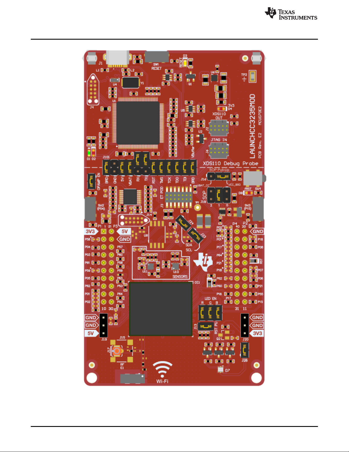
Figure 1-2 shows the CC3235MODSF LaunchPad EVM.
www.ti.com
Figure 1-2. CC3235MODSF LaunchPad™ EVM Overview
8
CC3235MODSF LaunchPad™ Development Kit (LAUNCHCC3235MOD)
Copyright © 2019, Texas Instruments Incorporated
SWRU548–February 2019
Submit Documentation Feedback
Page 9
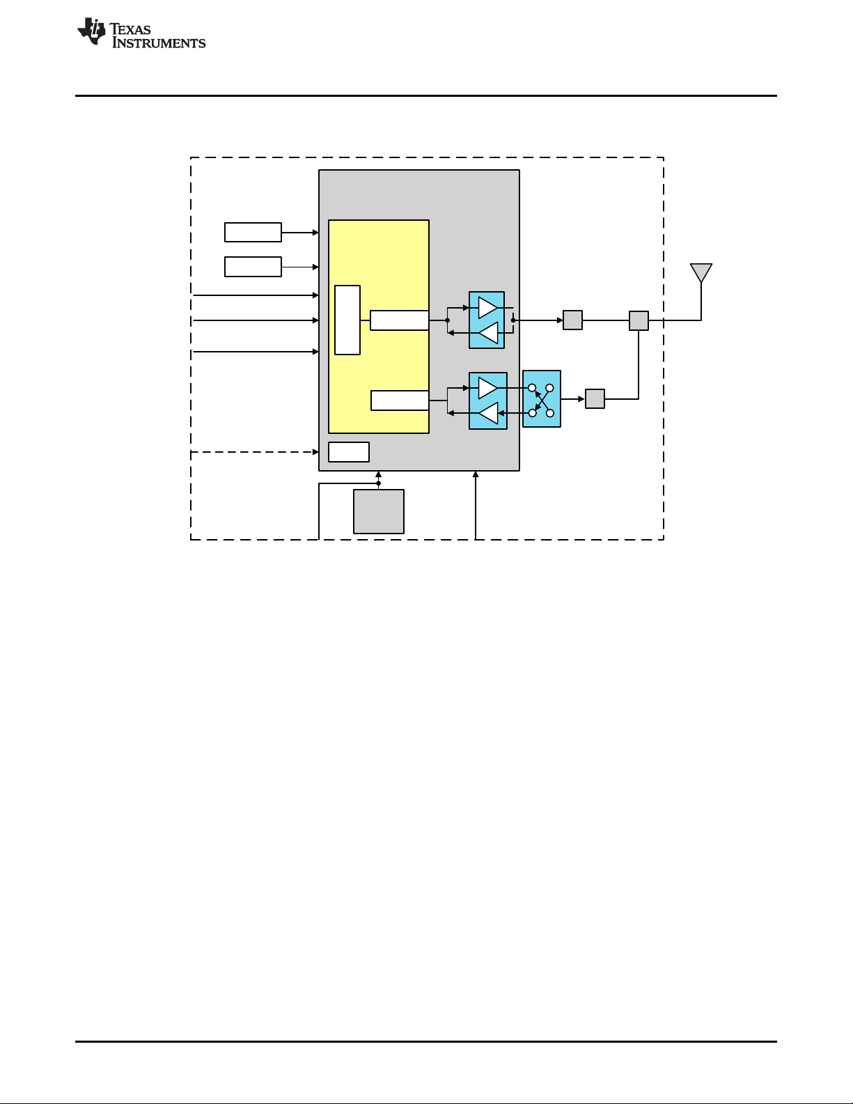
CC3235
MAC/PHY
WRF_BGN F
BGN
RF_ANT1
32-Mbit
SFlash
External SPI
Programming
40 MHz
32.768 kHz
UART
SPI
nReset
PM
2.3 V to 3.6 V
VBAT
User GPIOx
Aband
F
D
5 GHz
SPDT
WRF_A
www.ti.com
1.2.1 Block Diagram
Figure 1-3 shows a functional block diagram of the CC3235MODx module.
Hardware
Figure 1-3. CC3235MODx Functional Block Diagram
SWRU548–February 2019
Submit Documentation Feedback
CC3235MODSF LaunchPad™ Development Kit (LAUNCHCC3235MOD)
Copyright © 2019, Texas Instruments Incorporated
9
Page 10
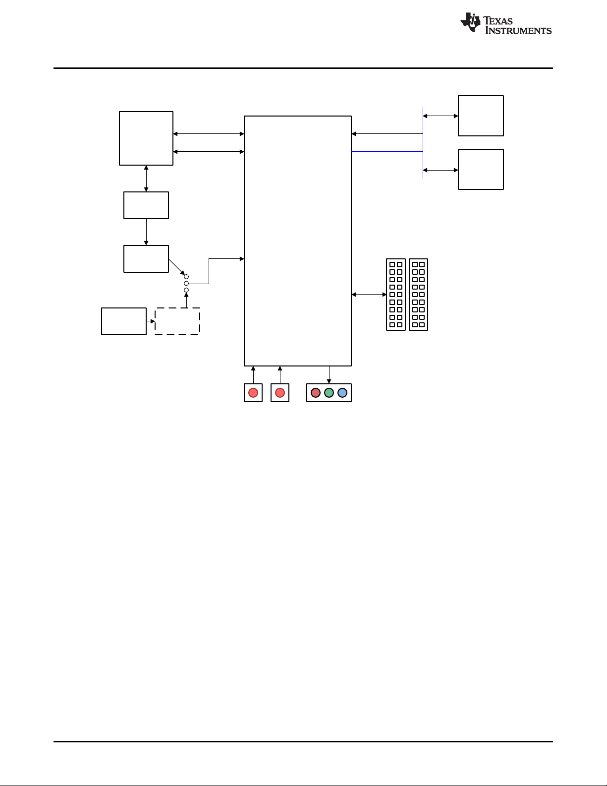
CC3235MODSF12MOBR
Acc
BMA280
Temperature
Sensor
TMP116
Two 20-pin LaunchPad headers
(compatible with TI MCU standard)
INT (GPIO13)
I2C
FTDI
FT2232D
and
SWD Circuit
USB
Connector
LDO
3.3 V
VCC
Two AA
Battery
Connectors
Reverse
Protection
Push buttons
GPIO13, GPIO22
RGB LED
GPIO9, GPIO10, GPIO11
JTAG and SWD
UART (Flashing)
Hardware
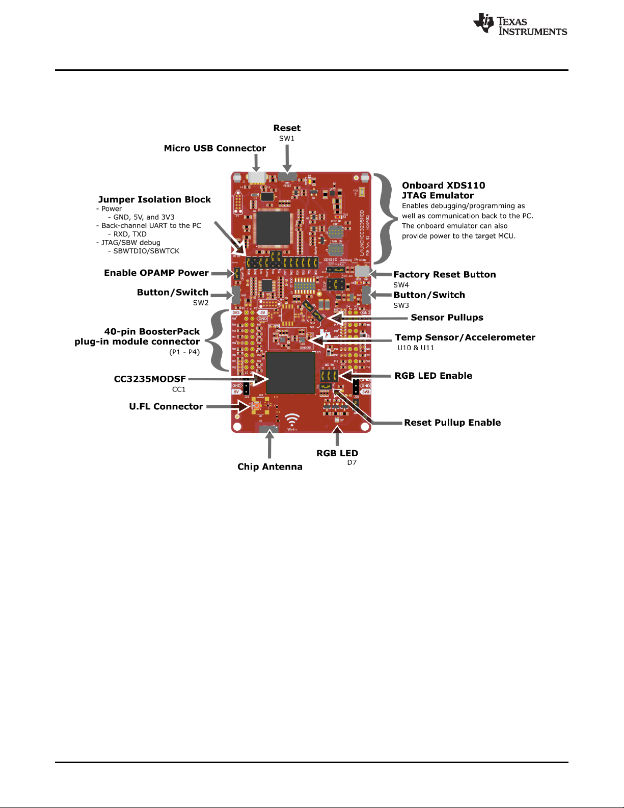
Figure 1-4 shows a functional block diagram of the LAUNCHCC3235MOD SimpleLink LaunchPad.
www.ti.com
Figure 1-4. LAUNCHCC3235MOD Functional Block Diagram
10
CC3235MODSF LaunchPad™ Development Kit (LAUNCHCC3235MOD)
Copyright © 2019, Texas Instruments Incorporated
SWRU548–February 2019
Submit Documentation Feedback
Page 11

www.ti.com
1.2.2 Hardware Features
• CC3235MODSF, SimpleLinkTMDual-Band Wi-Fi®module solution with integrated MCU
• 40-pin LaunchPad™ standard that leverages the BoosterPack™ ecosystem
• TI Standard XDS110-based JTAG emulation with serial port for flash programming
• Supports both 4-wire JTAG and 2-wire SWD
• Two buttons and a RGB LED for user interaction
• Virtual COM port UART through USB on PC
• Onboard chip antenna with U.FL or SMA for conducted testing, selectable using 0-Ω resistors
• Onboard accelerometer and temperature sensor for out-of-box demo, with the option to isolate them
from the inter-integrated circuit (I2C) bus
• Micro USB connector for power and debug connections
• Headers for current measurement and external JTAG connection, with an option to use the onboard
XDS110 to debug customer platforms
• Bus-powered device, with no external power required for Wi-Fi
• Long-range transmission with a highly optimized antenna (200-meter typical in open air with a 6-dBi
antenna AP)
• Can be powered externally, working down to 2.3 V
1.2.2.1 Key Benefits
The CC3235MODx modules offer the following benefits:
• Fully Integrated and Green/RoHS Modules Includes All Required Clocks, SPI Flash, and Passives
• 802.11 a/b/g/n: 2.4 GHz and 5 GHz
• FCC, IC/ISED, ETSI/CE, and MIC Certified
• FIPS 140-2 Level 1 Validated IC Inside
• Multilayered security features, help developers protect identities, data, and software IP
• Low-Power Modes for battery powered application
• Coexistence with 2.4 GHz Radios
• Industrial Temperature: –40°C to +85°C
• CC3235MODx Multiple-core architecture, system-on-chip (SoC)
• 1.27-mm Pitch QFM Package for Easy Assembly and Low-Cost PCB Design
• Transferrable Wi-Fi Alliance®Certification
• Application microcontroller subsystem:
– Arm®Cortex®-M4 core at 80 MHz
– User-dedicated memory
• 256 KB RAM
• Optional 1 MB executable Flash
– Rich set of peripherals and timers
– 26 I/O pins with flexible multiplexing options
• UART, I2S, I2C, SPI, SD, ADC, and 8-bit parallel interface
• 8-bit Synchronous Image Interface
• Timers and PWM
– Debug Interfaces: JTAG, cJTAG, and SWD
• Wi-Fi network processor subsystem:
– Wi-Fi®core:
• 802.11 a/b/g/n 2.4 GHz and 5 GHz
• Modes:
Hardware
®
SWRU548–February 2019
Submit Documentation Feedback
CC3235MODSF LaunchPad™ Development Kit (LAUNCHCC3235MOD)
Copyright © 2019, Texas Instruments Incorporated
11
Page 12

Hardware
• Multilayered security features:
• Application Throughput
• Power-Management Subsystem:
www.ti.com
• Access Point (AP)
• Station (STA)
• Wi-Fi Direct®(only supported on 2.4 GHz)
• Security:
• WEP
• WPA™/WPA2™ PSK
• WPA2 Enterprise
– Internet and application protocols:
• HTTPs server, mDNS, DNS-SD, DHCP
• IPv4 and IPv6 TCP/IP stack
• 16 BSD sockets (fully secured TLS v1.2 and SSL 3.0)
– Built-in power management subsystem:
• Configurable low-power profiles (always, intermittent, tag)
• Advanced low-power modes
• Integrated DC/DC regulators
– Separate execution environments
– Networking security
– Device identity and key
– Hardware accelerator cryptographic engines (AES, DES, SHA/MD5, CRC)
– Application-level security (encryption, authentication, access control)
– Initial secure programming
– Software tamper detection
– Secure boot
– Certificate signing request (CSR)
– Unique per device key pair
– UDP: 16 Mbps
– TCP: 13 Mbps
– Integrated DC/DC converters support a wide range of supply voltage:
• VBAT wide-voltage mode: 2.3 V to 3.6 V
• VIO is always tied with VBAT
– Advanced low-power modes:
• Shutdown: 1 µA, hibernate: 5 µA
• Low-power deep sleep (LPDS): 120 µA
• Idle connected (MCU in LPDS): 710 µA
• RX traffic (MCU active): 59 mA
• TX traffic (MCU active): 223 mA
– Wi-Fi TX Power
• 2.4 GHz: 16.5 dBm at 1 DSSS
• 5 GHz: 14.5 dBm at 6 OFDM
– Wi-Fi RX Sensitivity
• 2.4 GHz: –94.5 dBm at 1 DSSS
• 5 GHz: –89 dBm at 6 OFDM
12
CC3235MODSF LaunchPad™ Development Kit (LAUNCHCC3235MOD)
Copyright © 2019, Texas Instruments Incorporated
SWRU548–February 2019
Submit Documentation Feedback
Page 13

www.ti.com
• Additional Integrated Components
• Footprint Compatible QFM Package
• Module Supports SimpleLink Developer's Ecosystem
Hardware
– 40.0 MHz Crystal
– 32.768 kHz Crystal (RTC)
– 32 Mbit SPI Serial Flash
– RF Filters, Diplexer and Passive Components
– CC3235MODx: 1.27-mm Pitch,
63-Pin, 20.5-mm × 17.5-mm
SWRU548–February 2019
Submit Documentation Feedback
CC3235MODSF LaunchPad™ Development Kit (LAUNCHCC3235MOD)
Copyright © 2019, Texas Instruments Incorporated
13
Page 14
Hardware
1.2.2.2 XDS110-Based Onboard Debug Probe
To keep development easy and cost effective, TI's LaunchPad development kits integrate an onboard
debug probe, which eliminates the need for expensive programmers. The CC3235MODSF LaunchPad
has the XDS-110-based debug probe (see Figure 1-5), which is a simple and low-cost debugger that
supports nearly all TI Arm device derivatives.
www.ti.com
Figure 1-5. XDS-110 Debug Probe
The dotted line through J101 shown in Figure 1-5 divides the XDS110 debug probe from the target area.
The signals that cross this line can be disconnected by jumpers on J101, the isolation jumper block. More
details on the isolation jumper block are in Section 1.2.2.3.
The XDS110 debug probe also provides a "backchannel" UART-over-USB connection with the host, which
can be very useful during debugging and for easy communication with a PC. More details can be found in
Section 1.2.2.4.
The XDS110 debug probe hardware can be found in the schematics in Section 1.7.2 and in the hardware
design files.
1.2.2.3 Debug Probe Connection: Isolation Jumper Block
The isolation jumper block at jumper J101 allows the user to connect or disconnect signals that cross from
the XDS110 domain into the CC3235MOD target domain. This includes JTAG signals, application UART
signals, and 3.3-V and 5-V power.
Reasons to open these connections:
• To remove any and all influence from the XDS110 debug probe for high accuracy target power
measurements
• To control 3-V and 5-V power flow between the XDS110 and target domains
14
CC3235MODSF LaunchPad™ Development Kit (LAUNCHCC3235MOD)
Copyright © 2019, Texas Instruments Incorporated
SWRU548–February 2019
Submit Documentation Feedback
Page 15

www.ti.com
• To expose the target MCU pins for other use than onboard debugging and application UART
• To expose the programming and UART interface of the XDS110 so that it can be used for devices
Hardware
communication
other than the onboard MCU.
Table 1-1. Isolation Block Connections
Jumper Description
BRD Board Power. Supplies the board power from the onboard DC-
DC converter. The board power includes the sensors, LED, and
the OPAMP used to drive the ADC input.
GND Ground reference
5V 5-V VBUS from USB
VBAT 3.3-V rail, derived from VBUS in the XDS110 domain. Can also
be used to measure the current flowing into the CC3235MOD.
RX Backchannel UART: The target CC3235MODSF receives data
through this signal.
TX Backchannel UART: The target CC3235MODSF sends data
through this signal.
RST This pin functions as the RST signal (active low).
TMS Serial wire data input (SWDIO) / JTAG test mode select (TMS)
TCK Serial wire clock input (SWCLK) / JTAG clock input (TCK)
TDO JTAG test data out
TDI JTAG test data in
VBUFFER Used to power the level shifters located on the emulator side of
the board. The level shifters can be powered by shorting this pin
with a jumper. Removing the jumper enables low current
measurement.
1.2.2.4 Application (or "Backchannel") UART
The board supports a USB-based virtual COM port, using the Tiva™ ARM® MCU. The LaunchPad is
shipped with the UART lines from the CC3235MODSF connected to the UART on the Tiva MCU. The
CC3235MODSF's UART can also be routed to the 20-pin connector for use as a GPIO or external UART.
The selection is performed using jumpers on the board.
Figure 1-6 shows the UART routed to USB COM port. Ensure that a jumper is also placed on the
VBUFFER header to power the level shifters located on the emulator side of the board. Figure 1-7 shows
the UART routed to 20-pin header connector.
Figure 1-6. UART Routed to USB COM Port
SWRU548–February 2019
Submit Documentation Feedback
CC3235MODSF LaunchPad™ Development Kit (LAUNCHCC3235MOD)
Copyright © 2019, Texas Instruments Incorporated
15
Page 16

Hardware
1.2.2.5 JTAG Headers
The headers are provided on the board to isolate the CC3235MOD from the onboard XDS110-based
JTAG emulator. These jumpers are shorted by default when the board is shipped from TI. Figure 1-5 and
Table 1-1 are for default configurations, and Figure 1-8 shows the external emulator connection. To
connect an external emulator, remove the isolation block JTAG jumpers and place the external emulator
on the JTAG IN connector.
www.ti.com
Figure 1-7. UART Routed to 20-Pin Header Connector
16
Figure 1-8. JTAG IN Connector (J6)
CC3235MODSF LaunchPad™ Development Kit (LAUNCHCC3235MOD)
Copyright © 2019, Texas Instruments Incorporated
SWRU548–February 2019
Submit Documentation Feedback
Page 17

www.ti.com
1.2.2.6 Using the XDS110 Debug Probe with a Different Target
The XDS110 debug probe on the LaunchPad development kit can interface to most Arm Cortex-M
devices, not just the onboard target CC3235MODSF device. This functionality is enabled by the J2 10-pin
Cortex-M JTAG connector (See Figure 1-9) and a 10-pin cable, such as the FFSD-05-D-06.00-01-N (sold
separately from the LaunchPad development kit).
Hardware
Figure 1-9. XDS110 OUT Connector (J2)
Header J2 follows the Cortex-M Arm standard; however, pin 1 is not a voltage sense pin. The XDS110
outputs only 3.3-V JTAG signals. If another voltage level is needed, the user must provide level shifters to
translate the JTAG signal voltages.
1. Remove jumpers on the JTAG signals on the isolation block, including RST, TMS, TCK, TDO, and TDI.
2. Plug the 10-pin cable into J2, and connect to an external target.
a. J2 follows the Arm Cortex Debug Connector standard outlined in Cortex-M Debug Connectors.
3. Plug USB power into the LaunchPad development kit, or power it externally
a. JTAG levels are 3.3-V ONLY
SWRU548–February 2019
Submit Documentation Feedback
CC3235MODSF LaunchPad™ Development Kit (LAUNCHCC3235MOD)
Copyright © 2019, Texas Instruments Incorporated
17
Page 18

Hardware
1.2.2.7 Power Connections
The board accommodates various power methods, including through the onboard XDS110 as well as
external or BoosterPack plug-in module power (see Figure 1-10).
www.ti.com
Figure 1-10. LAUNCHCC3235MOD Power Block Diagram
18
CC3235MODSF LaunchPad™ Development Kit (LAUNCHCC3235MOD)
Copyright © 2019, Texas Instruments Incorporated
SWRU548–February 2019
Submit Documentation Feedback
Page 19

www.ti.com
1.2.2.7.1 XDS110 USB Power
The most common power-supply scenario is from USB through the XDS110 debugger. This provides 5-V
power from the USB and also regulates this power rail to 3.3 V for XDS110 operation and 3.3-V to the
target side of the LaunchPad development kit. Power from the XDS110 is controlled by jumper J101.
When the board is powered from the USB connector, ensure that the jumpers are placed on the following
headers, shown in Figure 1-11.
Hardware
SWRU548–February 2019
Submit Documentation Feedback
Figure 1-11. Powering the CC3235MODSF LP from USB
CC3235MODSF LaunchPad™ Development Kit (LAUNCHCC3235MOD)
Copyright © 2019, Texas Instruments Incorporated
19
Page 20

Hardware
1.2.2.7.2 BoosterPack Plug-in Module and External Power Supply
Headers J19 and J20 are present on the board to supply external power directly when USB power is not
available. Use the following precautions before using the board with an external power supply.
1. Remove the USB cable.
2. Ensure that jumpers are only placed on the headers shown in Figure 1-12.
3. Use a jumper wire to connect VBAT and BRD.
4. Plug in the external power supply on J20 with the correct polarity.
www.ti.com
20
Figure 1-12. Powering the CC3235MODSF LP from an External Power Supply
The OPAMP EN and LED EN jumpers are also available to remove any current draw from the onboard
OpAmp and LEDs being driven by the GPIOs, see Table 1-2.
CC3235MODSF LaunchPad™ Development Kit (LAUNCHCC3235MOD)
Copyright © 2019, Texas Instruments Incorporated
SWRU548–February 2019
Submit Documentation Feedback
Page 21

www.ti.com
Table 1-2. External Supply Connections and Enable Jumpers
Reference Use Comments
J19 5-V power input Used to power the board from an external 5-V supply
J20 3.3-V power input Used to power the board from an external 3.3-V supply.
J21 OPAMP EN If uninstalled, the power supply to the operational amplifier is cut off. This
J26 LED EN If uninstalled, the LEDs connected to the GPIO are disabled; this can be
1.2.2.8 Reset Pullup Jumper
Table 1-3 lists the reset pullup jumper.
Reference Use Comments
J13 RESET pullup Install this jumper to enable the pullup resistor on the nRESET pin of the
1.2.2.9 Clocking
All of the required clocks are inside the module. There is no need to supply any external clock.
Hardware
can be used to enable low-power measurements.
used to enable low-power measurements.
Table 1-3. Reset Pullup Jumper
device, when the board is powered from an external supply.
1.2.2.10 I2C Connection
The board features an accelerometer and a temperature sensor for the out-of-box demo. These are
connected to the I2C bus, and can be isolated using the jumpers provided (shown as yellow jumpers J23
and J24 in Figure 1-13).
Figure 1-13. I2C Connections
By removing J23 and J24, the accelerometer and the temperature sensors are isolated from the I2C bus.
This measure also removes the I2C pullup resistors from the sensor side of the circuit, and therefore any
connection to the circuit requires the user to install external pullup resistors.
Table 1-4 lists the I2C jumper definitions.
SWRU548–February 2019
Submit Documentation Feedback
CC3235MODSF LaunchPad™ Development Kit (LAUNCHCC3235MOD)
Copyright © 2019, Texas Instruments Incorporated
21
Page 22

Hardware
Reference Use Comments
J23 I2C SCL Populated: CC3235MOD SCL connected to onboard sensors with pullup
J24 I2C SDA Populated: CC3235MOD SDA connected to onboard sensors with pullup
1.2.2.10.1 Default I2C Addresses
Table 1-5 lists the default I2C addresses of the onboard sensors.
Table 1-5. Default I2C Addresses (of Onboard Sensors)
Sensor Type Reference Designator on LP Part Number (Manufacturer) Default Slave Address (Hex)
Temperature (Digital ) U10 TMP116 (TI) 0x92
Accelerometer (Triaxial) U11 BMA280 (Bosch) 0x30
1.2.2.11 Sense on Power (SOP)
The CC3235MODx device can be set to operate in four different modes based on the state of the sense
on power (SOP) lines. The SOP lines are pins 23, 24, and 34 on the CC3235MODx module. Table 1-6 the
state of the device, and Figure 1-14 shows the SOP jumpers.
www.ti.com
Table 1-4. I2C Jumper Definitions
Open: CC3235MOD SCL disconnected from onboard sensors
Open: CC3235MOD SDA disconnected from onboard sensors
Table 1-6. SOP[2:0]
Binary Value Function
100 Flash programming
000 Functional mode + 4-wire JTAG
001 Functional mode + SWD
010 Functional mode + flash
22
CC3235MODSF LaunchPad™ Development Kit (LAUNCHCC3235MOD)
Copyright © 2019, Texas Instruments Incorporated
SWRU548–February 2019
Submit Documentation Feedback
Page 23

www.ti.com
Hardware
NOTE: SOP[2:0] corresponds to J18 on the LaunchPad design.
Figure 1-14. SOP Jumpers (Default Setting Shown)
NOTE: Placing no jumpers on the block ensures that the line is pulled low using 100K pull down
resistors. Placing the jumper pulls the pin high using a 10K resistor.
1.2.2.12 Push-Buttons and LED Indicators
Table 1-7 lists the push-button definitions.
Table 1-7. Push-Button Definitions
Reference Use Comments
SW1 RESET This is used to reset the CC3235MOD device. This signal is also output on the
SW2 GPIO_13 When pushed, GPIO_13 is pulled to VCC.
SW3 GPIO_22 When pushed, GPIO_22 is pulled to VCC.
SW4 Factory default Pressing this button and toggling RESET restores the factory default image on
20-pin connector to reset any external BoosterPack which may be stacked. The
reset can be isolated using the RST jumper at the isolation block.
the serial flash. This can be used to recover a corrupted serial flash, provided
the s-flash was programmed with a recovery image.
SWRU548–February 2019
Submit Documentation Feedback
CC3235MODSF LaunchPad™ Development Kit (LAUNCHCC3235MOD)
Copyright © 2019, Texas Instruments Incorporated
23
Page 24

Hardware
Table 1-8 lists the LED indicators.
www.ti.com
Table 1-8. LED Indicators
Reference Color Use Comments
D1,D2 Green and Red Debug Indicates the state of the JTAG
D3 Yellow nRESET Indicates the state of the
D4 Red Power Indicates when the 3.3-V
D7 RGB GPIO_09 Glows when the GPIO is logic-
RGB GPIO_10 Glows when the GPIO is logic-
RGB GPIO_11
(1)
D8 Red Factory Reset Indicates that the push-button
emulator. For TI use only.
NRESET pin. If this LED is on,
the device is functional.
power is supplied to the board.
1.
1.
Glows when the GPIO is logic-
1.
for the factory reset is pressed.
(1)
GPIO_10 and GPIO_11 are also used as I2C. Whenever the pullups are enabled, the LEDs glow by default without configuring
the GPIOs.
24
CC3235MODSF LaunchPad™ Development Kit (LAUNCHCC3235MOD)
Copyright © 2019, Texas Instruments Incorporated
SWRU548–February 2019
Submit Documentation Feedback
Page 25

www.ti.com
1.2.3 BoosterPack Header Pin Assignment
The TI BoosterPack header pinout specification is at Build Your Own BoosterPack. Also see the BoosterPack Pinout Standard.
The CC3235MODSF LaunchPad follows this standard, with the exception of naming. (P1:P4 is used instead of J1:J4.). See Figure 1-15 for the
CC3235MODSF LaunchPad pin-mapping assignments and functions.
Hardware
NOTE: RESET output is an open-drain-type output and can only drive the pin low. The pullup ensures that the line is pulled back high when the
button is released. No external BoosterPack can drive this pin low.
All the signals are referred to by the pin number in the SDK; Figure 1-15 shows the default mappings. Some of the pins are repeated across the
connector. For instance, pin 62 is available on P1 and P4, but only P1 is connected by default. The signal on P4 is marked with an asterisk (*) to
signify that it is not connected by default. The signal can be routed to the pin by using a 0-Ω resistor in the path. For the exact resistor placement,
see the CC3235MODSF SimpleLinkTMWi-Fi® Wireless MCU LaunchPad Board Design Files.
SWRU548–February 2019
Submit Documentation Feedback
Figure 1-15. LAUNCHCC3235MOD BoosterPack Header Pin Assignments
CC3235MODSF LaunchPad™ Development Kit (LAUNCHCC3235MOD)
Copyright © 2019, Texas Instruments Incorporated
25
Page 26

Hardware
1.2.4 Electrical Characteristics
For electrical characteristics of the CC3235MODx modules, see CC3235MODx SimpleLink™ Wi-Fi®
CERTIFIED™ Wireless Module Solutions (S and SF).
1.2.5 Antenna Characteristics
The CC3235MODSM2MOB and the CC3235MODSF12MOB reference design detail the use of an onboard antenna. For more information on the antenna VSWR, efficiency, and electrical characteristics, see
M830520.
www.ti.com
26
CC3235MODSF LaunchPad™ Development Kit (LAUNCHCC3235MOD)
Copyright © 2019, Texas Instruments Incorporated
SWRU548–February 2019
Submit Documentation Feedback
Page 27

www.ti.com
1.3 Layout Guidelines
The integrator of the CC3235MODx modules must comply with the PCB layout recommendations
described in the following subsections to preserve and minimize the risk with regulatory certifications for
FCC, ISED/IC, ETSI/CE, and MIC. Also, TI recommends that customers follow the guidelines described in
this section to achieve similar performance.
1.3.1 LAUNCHCC3235MOD Board Layout
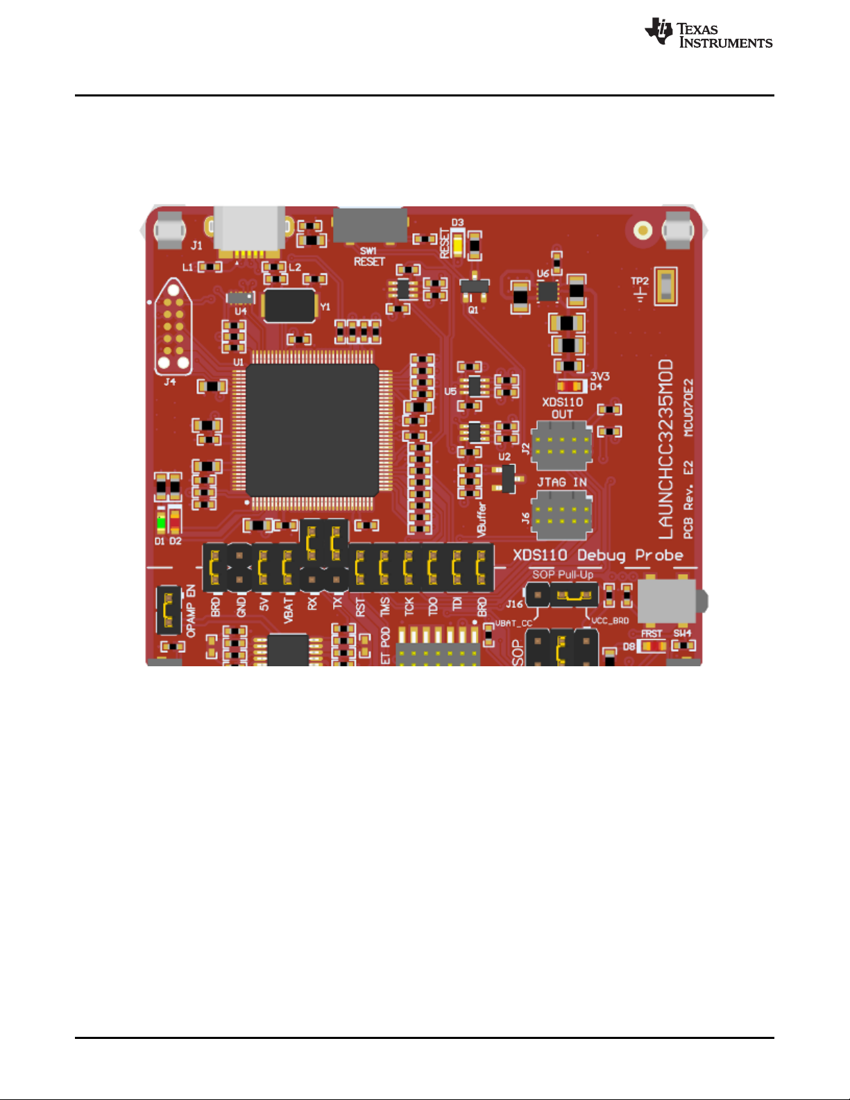
The reference layout consists of a four-layer design. Figure 1-16 shows the LAUNCHCC3235MOD top
layer.
Layout Guidelines
SWRU548–February 2019
Submit Documentation Feedback
Figure 1-16. LAUNCHCC3235MOD Top Layer
CC3235MODSF LaunchPad™ Development Kit (LAUNCHCC3235MOD)
Copyright © 2019, Texas Instruments Incorporated
27
Page 28
Layout Guidelines
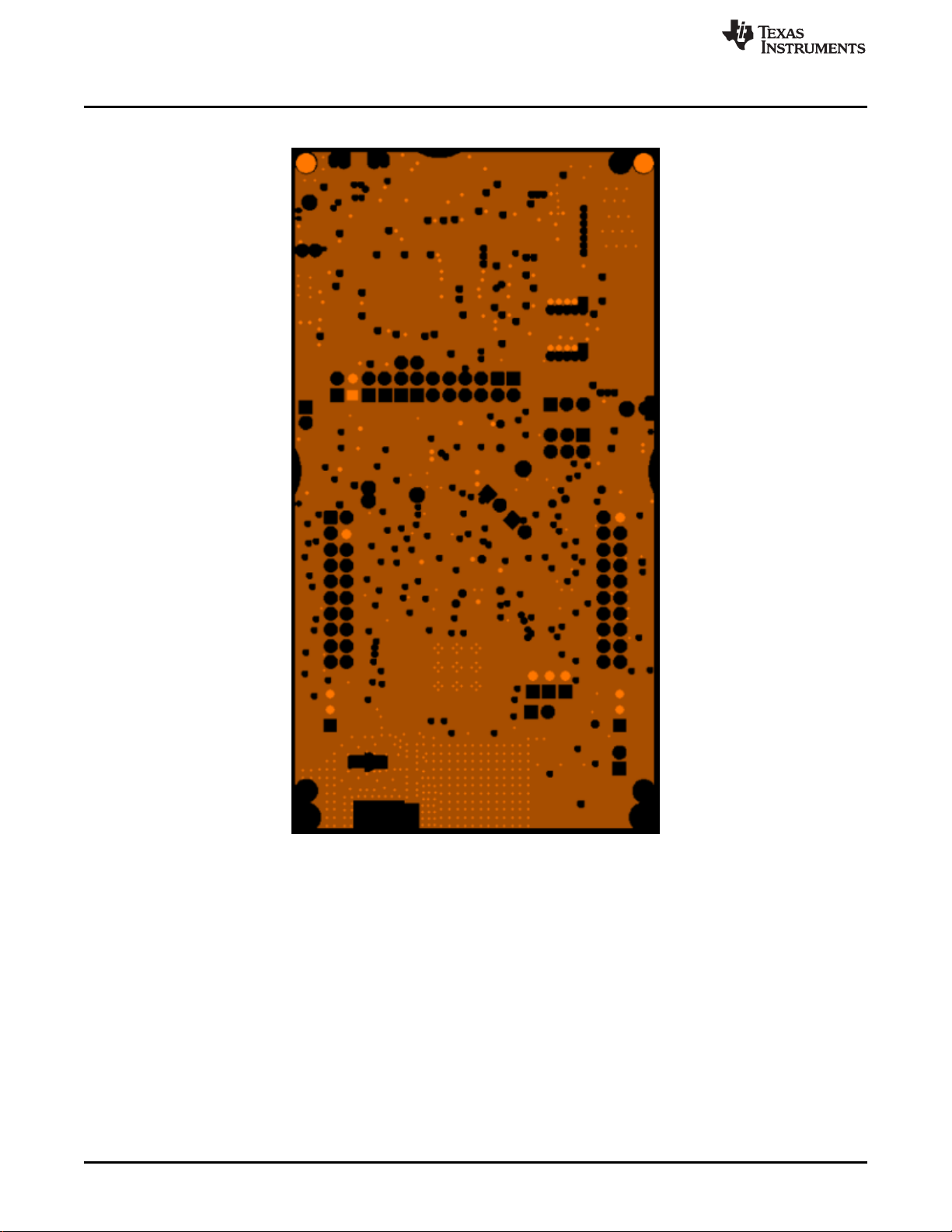
Figure 1-17 shows the LAUNCHCC3235MOD first inner layer.
www.ti.com
28
Figure 1-17. LAUNCHCC3235MOD First Inner Layer
CC3235MODSF LaunchPad™ Development Kit (LAUNCHCC3235MOD)
Copyright © 2019, Texas Instruments Incorporated
SWRU548–February 2019
Submit Documentation Feedback
Page 29
www.ti.com
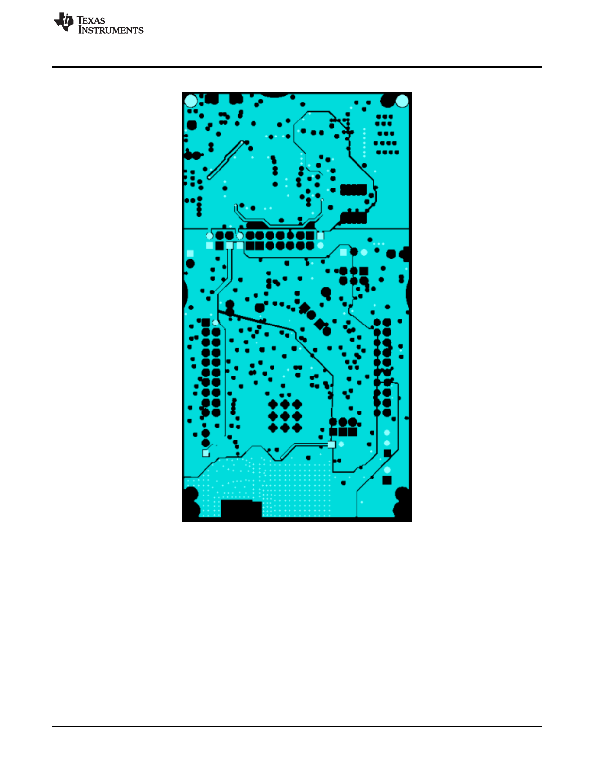
Figure 1-18 shows the LAUNCHCC3235MOD second inner layer.
Layout Guidelines
SWRU548–February 2019
Submit Documentation Feedback
Figure 1-18. LAUNCHCC3235MOD Second Inner Layer
CC3235MODSF LaunchPad™ Development Kit (LAUNCHCC3235MOD)
Copyright © 2019, Texas Instruments Incorporated
29
Page 30

Layout Guidelines
Figure 1-19 shows the LAUNCHCC3235MOD bottom layer.
www.ti.com
30
Figure 1-19. LAUNCHCC3235MOD Bottom Layer
CC3235MODSF LaunchPad™ Development Kit (LAUNCHCC3235MOD)
Copyright © 2019, Texas Instruments Incorporated
SWRU548–February 2019
Submit Documentation Feedback
Page 31

www.ti.com
1.3.2 General Layout Recommendations
Ensure that the following general layout recommendations are followed:
• Have a solid ground plane and ground vias under the module for stable system and thermal
dissipation.
• Do not run signal traces underneath the module on a layer where the module is mounted.
1.3.3 RF Layout Recommendations
The RF section of this wireless module gets top priority in terms of layout. It is very important for the RF
section to be laid out correctly to ensure optimum performance from the module. A poor layout can cause
low-output power, EVM degradation, sensitivity degradation, and mask violations.
Figure 1-20 shows the RF placement and routing of the CC3235MODSF module.
Layout Guidelines
Use the following RF layout recommendations for the CC3235MODx module:
• RF traces must have 50-Ω impedance.
• RF trace bends must be made with gradual curves, and 90 degree bends must be avoided.
• RF traces must not have sharp corners.
• There must be no traces or ground under the antenna section.
• RF traces must have via stitching on the ground plane beside the RF trace on both sides.
• RF traces must be as short as possible. The antenna, RF traces, and the module must be on the edge
SWRU548–February 2019
Submit Documentation Feedback
Figure 1-20. RF Section Layout
CC3235MODSF LaunchPad™ Development Kit (LAUNCHCC3235MOD)
Copyright © 2019, Texas Instruments Incorporated
31
Page 32

Copyright © 2017, Texas Instruments Incorporated
Layout Guidelines
of the PCB product in consideration of the product enclosure material and proximity.
For optimal RF performance, ensure the copper cut out on the top layer under the RF-BG pin (pin 31) is
as shown in Figure 1-21.
www.ti.com
Figure 1-21. Top Layer Copper Pullback on RF Pads
32
CC3235MODSF LaunchPad™ Development Kit (LAUNCHCC3235MOD)
Copyright © 2019, Texas Instruments Incorporated
SWRU548–February 2019
Submit Documentation Feedback
Page 33

www.ti.com
1.3.4 Antenna Placement and Routing
The antenna is the element used to convert the guided waves on the PCB traces to the free space
electromagnetic radiation. The placement and layout of the antenna are the keys to increased range and
data rates. Table 1-9 provides a summary of the recommended antennas to use with the CC3235MODx
module.
Table 1-9. Antenna Guidelines
SR NO. GUIDELINES
1 Place the antenna on an edge or corner of the PCB.
2
3
4
5
6
7 Ensure that the antenna has a near omnidirectional pattern.
8
Ensure that no signals are routed across the antenna elements on all the layers of the
PCB.
Most antennas, including the chip antenna used on the LaunchPad, require ground
clearance on all the layers of the PCB. Ensure that the ground is cleared on inner layers
as well.
Ensure that there is provision to place matching components for the antenna. These must
be tuned for best return loss when the complete board is assembled. Any plastics or
casing must also be mounted while tuning the antenna because this can impact the
impedance.
Ensure that the antenna impedance is 50 Ω because the module is rated to work only
with a 50-Ω system.
In case of printed antenna, ensure that the simulation is performed with the solder mask
in consideration.
The feed point of the antenna is required to be grounded. This is only for the antenna
type used on the CC3235MODx LaunchPad. See the specific antenna data sheets for the
recommendations.
Layout Guidelines
1.3.5 Transmission Line Considerations
The RF signal from the module is routed to the antenna using a Coplanar Waveguide with ground (CPWG) structure. CPW-G structure offers the maximum amount of isolation and the best possible shielding to
the RF lines. In addition to the ground on the L1 layer, placing GND vias along the line also provides
additional shielding. Figure 1-22 shows a cross section of the coplanar waveguide with the critical
dimensions.
Figure 1-22. Coplanar Waveguide (Cross Section)
SWRU548–February 2019
Submit Documentation Feedback
CC3235MODSF LaunchPad™ Development Kit (LAUNCHCC3235MOD)
Copyright © 2019, Texas Instruments Incorporated
33
Page 34

S
W
Layout Guidelines
Figure 1-23 shows the top view of the coplanar waveguide with GND and via stitching.
The recommended values for the PCB are provided for 2-layer boards in Table 1-10 and 4-layer boards in
Table 1-11.
www.ti.com
Figure 1-23. CPW With GND and Via Stitching (Top View)
Table 1-10. Recommended PCB Values for 2-Layer
Board (L1 to L2 = 42.1 mils)
PARAMETER VALUE UNIT
W 26 mils
S 5.5 mils
H 42.1 mils
Er (FR-4 substrate) 4.2 F/m
Table 1-11. Recommended PCB Values for 4-Layer
Board (L1 to L2 = 16 mils)
PARAMETER VALUE UNITS
W 21 mils
S 10 mils
H 16 mils
Er (FR-4 substrate) 4.5 F/m
34
CC3235MODSF LaunchPad™ Development Kit (LAUNCHCC3235MOD)
Copyright © 2019, Texas Instruments Incorporated
SWRU548–February 2019
Submit Documentation Feedback
Page 35

www.ti.com
1.4 Operational Setup and Testing
A compatible BoosterPack can be stacked on top of the LaunchPad using the two, 20-pin connectors. The
connectors do not have a key to prevent the misalignment of the pins or reverse connection. Ensure that
the VCC and 5-V pins are aligned with the BoosterPack header pins. On the CC3235MODSF LaunchPad,
a small white symbol is provided near pin 1 (see Figure 1-24) to orient all BoosterPacks.
Operational Setup and Testing
Figure 1-24. Pin 1 Marking on LaunchPad (3V3 Mark)
1.4.1 Measuring the CC3235MOD Current Draw
To measure the current draw of the CC3235MOD device using a multimeter, use the VBAT jumper on the
J101 isolation block. The current draw measured in this mode includes only the CC3235MOD device,
Serial Flash, any current drawn through the BoosterPack plug-in module headers. However, if a GPIO of
the CC3235MOD is driving a high current load like the LED, then that is also included in this
measurement.
1.4.1.1 Low-Current Measurement with USB Power (<1 mA)
See the following instructions to measure ultra-low power when powering with a USB cable (see ).
1. Remove the VBAT jumper in the J101 isolation block, and attach an ammeter across this jumper.
2. Consider the effect that the backchannel UART and any circuitry attached to the CC3235MOD may
have on current draw. Consider disconnecting these at the siolation jumper block, or at least consider
their current sinking and sourcing capability in the final measurement.
3. Begin target execution and set the device to low-power modes (LPDS or hibernate).
4. Measure the current. Remember that if the current levels are fluctuating, it may be difficult to get a
stable measurement. It is easier to measure quiescent states.
SWRU548–February 2019
Submit Documentation Feedback
Copyright © 2019, Texas Instruments Incorporated
CC3235MODSF LaunchPad™ Development Kit (LAUNCHCC3235MOD)
35
Page 36

Operational Setup and Testing
1.4.1.2 Active Current Measurements
See the following instructions to measure active power.
1. Remove the VBAT jumper (J18).
2. Solder a 0.1-Ω resistor on a wire which can be connected to a voltmeter/oscilloscope. Or, attach a
jumper across J18 so that it can be used with a current probe.
3. Measure the voltage across the resistor using an oscilloscope with a differential probe. For the current
probe, coil the wire around the sensor several times for good sensitivity.
• An ammeter can also be used for this measurement, but the results may be erroneous due to the
switching nature of the current
1.4.2 RF Connections
1.4.2.1 AP Connection Testing
By default, the board ships with the 2.4 GHz and 5 GHz RF signals routed to the onboard chip antenna,
as shown in .
www.ti.com
36
Figure 1-25. Using Onboard Antenna (Default Condition)
A U.FL connector J17 provides a way to test in the lab using a compatible cable. Alternatively, trackpads
for an SMA connector J15 are provided onboard to replace the J17 U.FL connector for testing conducted
measurements. A rework must be performed before these connectors can be used; this involves swapping
the position of a resistor. shows the modified board.
CC3235MODSF LaunchPad™ Development Kit (LAUNCHCC3235MOD)
Copyright © 2019, Texas Instruments Incorporated
SWRU548–February 2019
Submit Documentation Feedback
Page 37

www.ti.com
Figure 1-26. Board Modified for External Antenna Connections (Measure 2.4 GHz or 5 GHz)
1.4.3 Design Files
1.4.3.1 Hardware Design Files
Schematics can be found in Section 1.7.2.All design files, including schematics, layout, Bill of Materials
(BOM), Gerber files, and documentation are available for download from LAUNCHCC3235MOD.
Operational Setup and Testing
1.4.4 Software
All design files, including firmware patches, software example projects, and documentation are available
from the CC3235 Software Development Kit. Inside of the SDK, a set of very simple CC3235 code
examples can be found that demonstrates how to use the entire set of CC3235 peripherals. When starting
a new project or adding a new peripheral, these examples serve as a great starting point.
1.5 Development Environment Requirements
The following software examples with the LaunchPad require an integrated development environment
(IDE) that supports the CC3235MOD.
The CC3135 and CC3235 SimpleLink™ Wi-Fi® Embedded Programming User's Guide has detailed
information about software environment setup with examples. See this document for further details on the
software sample examples.
1.5.1 CCS
CCS 6.0 or higher is required. When CCS is launched, and a workspace directory is chosen, use Project
→ Import Existing CCS Eclipse Project. Direct it to the desired demo project directory containing main.c.
1.5.2 IAR
IAR 6.70 or higher is required. To open the demo in IAR, choose File → Open → Workspace…, and direct
it to the *.eww workspace file inside the \IAR subdirectory of the desired demo. All workspace information
is within this file.
The subdirectory also has an *.ewp project file; this file can be opened into an existing workspace, using
Project → Add-Existing-Project….
SWRU548–February 2019
Submit Documentation Feedback
CC3235MODSF LaunchPad™ Development Kit (LAUNCHCC3235MOD)
Copyright © 2019, Texas Instruments Incorporated
37
Page 38

Additional Resources
1.6 Additional Resources
1.6.1 CC3235MODx Product Page
For more information on the CC3235MOD device, visit the CC3235MOD product page, which includes the
CC3235MODx SimpleLink™ Wi-Fi® Wireless and Internet-of-Things Solution, a Single-Chip Wireless
MCU Data Sheet and key documents such as the CC32xx SimpleLink™ Wi-Fi® and Internet-of-Things
Technical Reference Manual.
1.6.2 Download CCS, IAR
Although the files can be viewed with any text editor, more can be done with the projects if they are
opened with a development environment such as Code Composer Studio (CCS), IAR, or Energia. CCS
and IAR are each available in a full version, or a free, code-size-limited version. The full out-of-box demo
cannot be built with the free version of CCS or IAR (IAR Kickstart), due to the code-size limit. To bypass
this limitation, a code-size-limited CCS version is provided that has most functionality integrated into a
library. The code built into the library is able to be viewed by the user, but it cannot be edited. For full
functionality, download the full version of either CCS or IAR.
1.6.3 SimpleLink™ Academy for CC3235 SDK
The SimpleLink™ Academy is a collection of curated training modules developed by TI subject matter
experts to help developers get up and running as quickly as possible with a SimpleLink MCU device and
its SDK. The training is delivered using TI Resource Explorer, which offers a powerful cloud-enabled
environment that includes background information, interactive exercises, code snippets, quizzes, and
more.
Experience the SimpleLink™ Academy now using the TI Resource Explorer at dev.ti.com.
www.ti.com
1.6.4 TI E2E Community
Search the forums at e2e.ti.com. If you cannot find your answer, post your question to the community!
38
CC3235MODSF LaunchPad™ Development Kit (LAUNCHCC3235MOD)
Figure 1-27. CC32xx SimpleLink™ Academy
Copyright © 2019, Texas Instruments Incorporated
SWRU548–February 2019
Submit Documentation Feedback
Page 39

www.ti.com
1.7 Assembly Drawing and Schematics
1.7.1 Assembly Drawing
Assembly Drawing and Schematics
Figure 1-28. LAUNCHCC3235MOD Top-Layer Assembly Drawing
SWRU548–February 2019
Submit Documentation Feedback
CC3235MODSF LaunchPad™ Development Kit (LAUNCHCC3235MOD)
Copyright © 2019, Texas Instruments Incorporated
39
Page 40

Assembly Drawing and Schematics
1.7.2 Schematics
www.ti.com
40
CC3235MODSF LaunchPad™ Development Kit (LAUNCHCC3235MOD)
Figure 1-29. Schematics (1 of 5)
SWRU548–February 2019
Submit Documentation Feedback
Copyright © 2019, Texas Instruments Incorporated
Page 41

www.ti.com
Assembly Drawing and Schematics
SWRU548–February 2019
Submit Documentation Feedback
Figure 1-30. Schematics (2 of 5)
CC3235MODSF LaunchPad™ Development Kit (LAUNCHCC3235MOD)
Copyright © 2019, Texas Instruments Incorporated
41
Page 42

Assembly Drawing and Schematics
www.ti.com
42
CC3235MODSF LaunchPad™ Development Kit (LAUNCHCC3235MOD)
Figure 1-31. Schematics (3 of 5)
SWRU548–February 2019
Submit Documentation Feedback
Copyright © 2019, Texas Instruments Incorporated
Page 43

www.ti.com
Assembly Drawing and Schematics
SWRU548–February 2019
Submit Documentation Feedback
Figure 1-32. Schematics (4 of 5)
CC3235MODSF LaunchPad™ Development Kit (LAUNCHCC3235MOD)
Copyright © 2019, Texas Instruments Incorporated
43
Page 44

Assembly Drawing and Schematics
www.ti.com
44
CC3235MODSF LaunchPad™ Development Kit (LAUNCHCC3235MOD)
Figure 1-33. Schematics (5 of 5)
SWRU548–February 2019
Submit Documentation Feedback
Copyright © 2019, Texas Instruments Incorporated
Page 45

IMPORTANT NOTICE AND DISCLAIMER
TI PROVIDES TECHNICAL AND RELIABILITY DATA (INCLUDING DATASHEETS), DESIGN RESOURCES (INCLUDING REFERENCE
DESIGNS), APPLICATION OR OTHER DESIGN ADVICE, WEB TOOLS, SAFETY INFORMATION, AND OTHER RESOURCES “AS IS”
AND WITH ALL FAULTS, AND DISCLAIMS ALL WARRANTIES, EXPRESS AND IMPLIED, INCLUDING WITHOUT LIMITATION ANY
IMPLIED WARRANTIES OF MERCHANTABILITY, FITNESS FOR A PARTICULAR PURPOSE OR NON-INFRINGEMENT OF THIRD
PARTY INTELLECTUAL PROPERTY RIGHTS.
These resources are intended for skilled developers designing with TI products. You are solely responsible for (1) selecting the appropriate
TI products for your application, (2) designing, validating and testing your application, and (3) ensuring your application meets applicable
standards, and any other safety, security, or other requirements. These resources are subject to change without notice. TI grants you
permission to use these resources only for development of an application that uses the TI products described in the resource. Other
reproduction and display of these resources is prohibited. No license is granted to any other TI intellectual property right or to any third
party intellectual property right. TI disclaims responsibility for, and you will fully indemnify TI and its representatives against, any claims,
damages, costs, losses, and liabilities arising out of your use of these resources.
TI’s products are provided subject to TI’s Terms of Sale (www.ti.com/legal/termsofsale.html) or other applicable terms available either on
ti.com or provided in conjunction with such TI products. TI’s provision of these resources does not expand or otherwise alter TI’s applicable
warranties or warranty disclaimers for TI products.
Mailing Address: Texas Instruments, Post Office Box 655303, Dallas, Texas 75265
Copyright © 2019, Texas Instruments Incorporated
 Loading...