


CC3235MODS, CC3235MODSF, CC3235MODAS, CC3235MODASF
www.ti.com
CC3235MODS, CC3235MODSF, CC3235MODAS, CC3235MODASF
SWRS243A – FEBRUARY 2020 – REVISED MAY 2020
SWRS243A – FEBRUARY 2020 – REVISED MAY 2020
CC3235MODx and CC3235MODAx SimpleLink™ Wi-Fi CERTIFIED™ Dual-Band
Wireless MCU Modules
1 Features
• Fully integrated and green and RoHS modules
include all required clocks, SPI flash, and passives
• 802.11a/b/g/n: 2.4 GHz and 5 GHz
• FCC, IC/ISED, ETSI/CE, MIC, and SRRC 1certified
• FIPS 140-2 Level 1 validated IC inside
• Multilayered security features help developers
protect identities, data, and software IP
• Low-power modes for battery-powered
applications
• Coexistence with 2.4-GHz radios
• Industrial temperature: –40°C to +85°C
• CC3235MODx multiple-core architecture, systemon-chip (SoC)
• CC3235MODAx modules include an integrated
PCB antenna for easy integration into the host
system
• 1.27-mm pitch QFM package for easy assembly
and low-cost PCB design
• Transferrable Wi-Fi Alliance® certification
• Application microcontroller subsystem:
– Arm® Cortex®-M4 core at 80 MHz
– User-dedicated memory
• 256KB of RAM
• Optional 1MB of executable flash
– Rich set of peripherals and timers
• McASP supports two I2S channels
• SD, SPI, I2C, UART
• 8-bit synchronous imager interface
• 4-channel 12-bit ADCs
• 4 general-purpose timers (GPT) with 16-bit
PWM mode
• Watchdog timer
• Up to 27 GPIO pins
• Debug interfaces: JTAG, cJTAG, SWD
• Wi-Fi network processor subsystem:
– Wi-Fi® core:
• 802.11 a/b/g/n 2.4 GHz and 5 GHz
• Modes:
– Access point (AP)
– Station (STA)
– Wi-Fi Direct® (only supported on 2.4
GHz)
• Security:
– WEP
– WPA™/ WPA2™ PSK
– WPA2 Enterprise
– WPA3™ Personal
– Internet and application protocols:
• HTTPs server, mDNS, DNS-SD, DHCP
• IPv4 and IPv6 TCP/IP stack
• 16 BSD sockets (fully secured TLS v1.2 and
SSL 3.0)
– Built-in power management subsystem:
• Configurable low-power profiles (always on,
intermittently connected, tag)
• Advanced low-power modes
• Integrated DC/DC regulators
• Multilayered security features:
– Separate execution environments
– Networking security
– Device identity and key
– Hardware accelerator cryptographic engines
(AES, DES, SHA/MD5, CRC)
– File system security (encryption, authentication,
access control)
– Initial secure programming
– Software tamper detection
– Secure boot
– Certificate signing request (CSR)
– Unique per device key pair
• Application throughput
– UDP: 16 Mbps
– TCP: 13 Mbps
• Power-Management Subsystem:
– Integrated DC/DC converters support a wide
range of supply voltage:
• Single wide-voltage supply, VBAT: 2.3 V to
3.6 V
– Advanced low-power modes:
• Shutdown: 1 µA, Hibernate: 5.5 µA
• Low-power deep sleep (LPDS): 120 µA
• Idle connected (MCU in LPDS): 710 µA
• RX traffic (MCU active): 59 mA
• TX traffic (MCU active): 223 mA
1
Contact TI for more information on using SRRC ID Certification: www.ti.com/tool/SIMPLELINK-CC3XXX-
CERTIFICATION
An IMPORTANT NOTICE at the end of this data sheet addresses availability, warranty, changes, use in safety-critical applications,
Copyright © 2020 Texas Instruments Incorporated
intellectual property matters and other important disclaimers. PRODUCTION DATA.
Product Folder Links: CC3235MODS CC3235MODSF CC3235MODAS CC3235MODASF
Submit Document Feedback
1

CC3235MODS, CC3235MODSF, CC3235MODAS, CC3235MODASF
SWRS243A – FEBRUARY 2020 – REVISED MAY 2020
www.ti.com
– Wi-Fi TX power
• 2.4 GHz: 16 dBm at 1 DSSS
• 5 GHz: 15.1 dBm at 6 OFDM
– Wi-Fi RX sensitivity
• 2.4 GHz: –94.5 dBm at 1 DSSS
• 5 GHz: –89 dBm at 6 OFDM
• Additional integrated components
– 40.0-MHz crystal
– 32.768-kHz crystal (RTC)
– 32Mbit SPI serial flash
– RF filters, diplexer and passive components
• Footprint-compatible QFM package
– CC3235MODx: 1.27-mm pitch,
63-pin, 20.5-mm × 17.5-mm
– CC3235MODAx: 1.27-mm pitch,
63-pin, 20.5-mm × 25.0-mm
• Module supports the SimpleLink Developer's
2 Applications
• For Internet of Things applications, such as:
– Medical and Healthcare
• Multiparameter Patient Monitor
• Electrocardiogram (ECG)
• Electronic Hospital Bed & Bed Control
• Telehealth Systems
– Building and Home Automation:
• HVAC Systems & Thermostat
• Video Surveillance, Video Doorbells, and
Low-Power Camera
• Building Security Systems and E-locks
– Appliances
– Asset Tracking
– Factory Automation
– Grid Infrastructure
Ecosystem
3 Description
Start your design with the fully programmable FCC, IC/ISED, ETSI/CE, MIC, and SRRC certified wireless
microcontroller (MCU) module with built-in dual-band Wi-Fi connectivity. The modules integrate the 40-MHz
crystal, 32.768-kHz RTC clock, 32Mb SPI serial flash, RF filters, diplexer, and passive components.
The SimpleLink™ CC3235MODx module is available in two variants:
• CC3235MODS includes 256KB of RAM, IoT networking security, device identity and keys, and MCU-level
security features such as file system encryption, user IP (MCU image) encryption, secure boot, and debug
security.
• CC3235MODSF builds on the CC3235MODS and integrates a user-dedicated 1MB of executable flash in
addition to the 256KB of RAM.
The SimpleLink™ CC3235MODAx module is available in two variants:
• CC3235MODAS includes 256KB of RAM, IoT networking security, device identity and keys, and MCU-level
security features such as file system encryption, user IP (MCU image) encryption, secure boot, and debug
security.
• CC3235MODASF builds on the CC3235MODAS and integrates a user-dedicated 1MB of executable flash in
addition to the 256KB of RAM.
Created for IoT, the SimpleLink™ Wi-Fi® CC3235MODx and CC3235MODAx module family from Texas
Instruments is a wireless module that integrates two physically separated on-chip MCUs.
• Application processor— Arm® Cortex®-M4 MCU with a user-dedicated 256KB of RAM and an optional 1MB
of executable flash.
• Network processor to run all Wi-Fi and Internet logical layers. This ROM-based subsystem completely
offloads the host MCU and includes an 802.11 a/b/g/n dual-band 2.4-GHz and 5-GHz radio, baseband, and
MAC with a powerful hardware cryptography engine.
This generation introduces new capabilities that further simplify the connectivity of things to the Internet. The
main new features include:
• 802.11a/b/g/n: 2.4-GHz and 5-GHz support
• 2.4-GHz coexistence with Bluetooth ® low energy radio
• Antenna diversity
• Enhanced security with FIPS 140-2 Level 1 validated IC inside: certification.
• More concurrent secure sockets (up to 16)
• Certificate signing request (CSR)
2 Submit Document Feedback
Product Folder Links: CC3235MODS CC3235MODSF CC3235MODAS CC3235MODASF
Copyright © 2020 Texas Instruments Incorporated

www.ti.com
SWRS243A – FEBRUARY 2020 – REVISED MAY 2020
• Online certificate status protocol (OCSP)
• Wi-Fi Alliance® certified for IoT applications with low-power capabilities and more
• Hostless mode for offloading template packet transmissions
• Improved fast scan
The CC3235MODx and CC3235MODAx device family is part of the SimpleLink MCU platform—a common,
easy-to-use development environment based on a single-core software development kit (SDK) with a rich tool
set and reference designs. The E2E™ support forums support Wi-Fi, Bluetooth low energy, Sub-1 GHz, and host
MCUs. For more information, visit www.ti.com/simplelink or www.ti.com/simplelinkwifi.
CC3235MODS, CC3235MODSF, CC3235MODAS, CC3235MODASF
Device Information
PART NUMBER PACKAGE BODY SIZE (NOM)
CC3235MODSM2MOB QFM (63) 20.5 mm × 17.5 mm
CC3235MODSF12MOB QFM (63) 20.5 mm × 17.5 mm
CC3235MODASM2MON QFM (63) 20.5 mm × 25 mm
CC3235MODASF12MON QFM (63) 20.5 mm × 25 mm
(1) For more information, see Section 13.
(1)
Copyright © 2020 Texas Instruments Incorporated
Product Folder Links: CC3235MODS CC3235MODSF CC3235MODAS CC3235MODASF
Submit Document Feedback
3

CC3235
MAC/PHY
WRF_BGN F
BGN
RF_ABG
32-Mbit
SFlash
External SPI
Programming
40 MHz
32.768 kHz
UART
SPI
nReset
PM
2.3 V to 3.6 V
VBAT
User GPIOx
Aband
F
D
5 GHz
SPDT
WRF_A
CC3235MODS, CC3235MODSF, CC3235MODAS, CC3235MODASF
SWRS243A – FEBRUARY 2020 – REVISED MAY 2020
4 Functional Block Diagrams
Figure 4-1 shows the functional block diagram of the CC3235MODx module.
www.ti.com
Figure 4-1. CC3235MODx Functional Block Diagram
4 Submit Document Feedback
Product Folder Links: CC3235MODS CC3235MODSF CC3235MODAS CC3235MODASF
Copyright © 2020 Texas Instruments Incorporated

CC3235
MAC/PHY
WRF_BGN F
BGN
RF_ABG
32-Mbit
SFlash
External SPI
Programming
40 MHz
32.768 kHz
UART
SPI
nReset
PM
2.3 V to 3.6 V
VBAT
User GPIOx
Aband
F
D
5 GHz
SPDT
WRF_A
www.ti.com
SWRS243A – FEBRUARY 2020 – REVISED MAY 2020
Figure 4-2 shows the functional block diagram of the CC3235MODAx module.
CC3235MODS, CC3235MODSF, CC3235MODAS, CC3235MODASF
Figure 4-2. CC3235MODAx Functional Block Diagram
Copyright © 2020 Texas Instruments Incorporated
Product Folder Links: CC3235MODS CC3235MODSF CC3235MODAS CC3235MODASF
Submit Document Feedback
5

CC32xx ± Single-Chip Wireless MCU
ARM
Cortex-M4
80 MHz
1-MB Flash (optional)
256-KB RAM
ROM
Peripherals
1x SPI
2x UART
1x I2C
1x I2S/PCM
1x SD/MMC
8-bit Camera
4x ADC
System
DMA
Timers
GPIOs
Network Processor
Application
Protocols
RAM
ROM
Crypto Engine
Wi-Fi Driver
TCP/IP Stack
(ARM Cortex)
Power
Management
Oscillators
DC-DC
RTC
Baseband
MAC
Processor
Radio
Synthesizer
Dual Band
Wi-Fi
COEX I/Os
Antenna Selection
CC3235MODS, CC3235MODSF, CC3235MODAS, CC3235MODASF
SWRS243A – FEBRUARY 2020 – REVISED MAY 2020
Figure 4-3 shows the an overview of the CC3235x hardware.
www.ti.com
6 Submit Document Feedback
Product Folder Links: CC3235MODS CC3235MODSF CC3235MODAS CC3235MODASF
Figure 4-3. CC3235x Hardware Overview
Copyright © 2020 Texas Instruments Incorporated

Customer Application
Peripherals
Driver
SimpleLink Driver APIs
NetApp
BSD
Socket
Wi-Fi
Host Interface
Network Applications
WLAN Security
and
Management
TCP/IP Stack
WLAN MAC and PHY
Applications MCU
Network Processor
www.ti.com
CC3235MODS, CC3235MODSF, CC3235MODAS, CC3235MODASF
Figure 4-4 shows the an overview of the CC3235x embedded software.
Figure 4-4. CC3235x Embedded Software Overview
SWRS243A – FEBRUARY 2020 – REVISED MAY 2020
Copyright © 2020 Texas Instruments Incorporated
Submit Document Feedback
Product Folder Links: CC3235MODS CC3235MODSF CC3235MODAS CC3235MODASF
7

CC3235MODS, CC3235MODSF, CC3235MODAS, CC3235MODASF
SWRS243A – FEBRUARY 2020 – REVISED MAY 2020
Table of Contents
www.ti.com
1 Features............................................................................1
2 Applications..................................................................... 2
3 Description.......................................................................2
4 Functional Block Diagrams............................................ 4
5 Revision History.............................................................. 8
6 Device Comparison......................................................... 9
6.1 Related Products...................................................... 12
7 Terminal Configuration and Functions........................13
7.1 CC3235MODx and CC3235MODAx Pin Diagram.... 13
7.2 Pin Attributes and Pin Multiplexing........................... 14
7.3 Signal Descriptions................................................... 31
7.4 Drive Strength and Reset States for Analog-
Digital Multiplexed Pins............................................... 36
7.5 Pad State After Application of Power to Chip, but
Before Reset Release................................................. 36
7.6 Connections for Unused Pins................................... 36
8 Specifications................................................................ 37
8.1 Absolute Maximum Ratings...................................... 37
8.2 ESD Ratings............................................................. 37
8.3 Recommended Operating Conditions.......................37
8.4 Current Consumption (CC3235MODS and
CC3235MODAS).........................................................38
8.5 Current Consumption (CC3235MODSF and
CC3235MODASF).......................................................40
8.6 TX Power Control for 2.4 GHz Band.........................42
8.7 TX Power Control for 5 GHz..................................... 44
8.8 Brownout and Blackout Conditions........................... 44
8.9 Electrical Characteristics for GPIO Pins................... 46
8.10 CC3235MODAx Antenna Characteristics............... 48
8.11 WLAN Receiver Characteristics..............................48
8.12 WLAN Transmitter Characteristics..........................49
8.13 BLE and WLAN Coexistence Requirements...........50
8.14 Reset Requirement................................................. 50
8.15 Thermal Resistance Characteristics for MOB
and MON Packages.................................................... 50
8.16 Timing and Switching Characteristics..................... 51
9 Detailed Description......................................................64
9.1 Overview................................................................... 64
9.2 Functional Block Diagram......................................... 64
9.3 Arm Cortex-M4 Processor Core Subsystem.............65
9.4 Wi-Fi Network Processor Subsystem....................... 66
9.5 Security..................................................................... 68
9.6 FIPS 140-2 Level 1 Certification............................... 70
9.7 Power-Management Subsystem...............................70
9.8 Low-Power Operating Mode..................................... 70
9.9 Memory..................................................................... 73
9.10 Restoring Factory Default Configuration.................75
9.11 Boot Modes.............................................................75
9.12 Hostless Mode........................................................ 76
9.13 Device Certification and Qualification..................... 77
9.14 Module Markings.....................................................79
9.15 End Product Labeling..............................................80
9.16 Manual Information to the End User....................... 80
10 Applications, Implementation, and Layout............... 81
10.1 Typical Application.................................................. 81
10.2 Device Connection and Layout Fundamentals....... 88
10.3 PCB Layout Guidelines...........................................88
11 Environmental Requirements and SMT
Specifications................................................................95
11.1 PCB Bending...........................................................95
11.2 Handling Environment.............................................95
11.3 Storage Condition................................................... 95
11.4 PCB Assembly Guide..............................................95
11.5 Baking Conditions................................................... 96
11.6 Soldering and Reflow Condition..............................97
12 Device and Documentation Support..........................98
12.1 Development Tools and Software........................... 98
12.2 Firmware Updates...................................................99
12.3 Device Nomenclature..............................................99
12.4 Documentation Support........................................ 100
12.5 Related Links........................................................ 101
12.6 Support Resources............................................... 102
12.7 Trademarks...........................................................102
13 Mechanical, Packaging, and Orderable
Information.................................................................. 103
13.1 Mechanical, Land, and Solder Paste Drawings.... 103
13.2 Package Option Addendum.................................. 103
5 Revision History
Changes from February 1, 2020 to August 20, 2020 (from Revision * (Feb 2020) to Revision A
(Aug 2020)) Page
• Added pins 20, 33, 39, 41, and 45 to Section 7.2.1 .........................................................................................15
• Added Pin 39 to list of No Connect pins in Table 7-4 .......................................................................................36
• Updated Coexistence Solution with Wi-Fi Antenna Selection and Dedicated BLE Antenna image. ............... 82
8 Submit Document Feedback
Product Folder Links: CC3235MODS CC3235MODSF CC3235MODAS CC3235MODASF
Copyright © 2020 Texas Instruments Incorporated

www.ti.com
SWRS243A – FEBRUARY 2020 – REVISED MAY 2020
6 Device Comparison
Table 6-2 shows the features supported across different CC3x35 modules.
Table 6-1. Device Features Comparison
CC3235MODS, CC3235MODSF, CC3235MODAS, CC3235MODASF
FEATURE
On-board chip CC3135 CC3235S CC3235SF
On-board ANT No No No
sFlash 32-Mbit 32-Mbit 32-Mbit
Regulatory certifications FCC, IC/ISED, ETSI/CE, MIC FCC, IC/ISED, ETSI/CE, MIC FCC, IC/ISED, ETSI/CE, MIC
Wi-Fi Alliance® Certification Yes Yes Yes
Input voltage 2.3 V to 3.6 V 2.3 V to 3.6 V 2.3 V to 3.6 V
Package 17.5 mm × 20.5 mm QFM 17.5 mm × 20.5 mm QFM 17.5 mm × 20.5 mm QFM
Operating temperature range –40°C to +85°C –40°C to +85°C –40°C to +85°C
Classification Wi-Fi Network Processor Wireless Microcontroller Wireless Microcontroller
Standard 802.11 a/b/g/n 802.11 a/b/g/n 802.11 a/b/g/n
Frequency 2.4 GHz, 5 GHz 2.4 GHz, 5 GHz 2.4 GHz, 5 GHz
TCP/IP Stack IPv4, IPv6 IPv4, IPv6 IPv4, IPv6
Secured sockets 16 16 16
Integrated MCU – Arm Cortex-M4 at 80 MHz Arm Cortex-M4 at 80 MHz
RAM – 256KB 256KB
Flash – – 1MB
Universal Asynchronous
Receiver/Transmitter (UART)
Serial Port Interface (SPI) 1 1 1
Multichannel Audio Serial Port (McASP)- I2S or PCM – 2-ch 2-ch
Inter-Integrated Circuit (I2C) – 1 1
Analog-to-digital converter (ADC) – 4-ch, 12-bit 4-ch, 12-bit
Parallel interface (8-bit PI) – 1 1
General-purpose timers – 4 4
Multimedia card (MMC / SD) – 1 1
CC3135MOD CC3235MODS CC3235MODSF
ON-CHIP APPLICATION MEMORY
PERIPHERALS AND INTERFACES
1 2 2
SECURITY FEATURES
DEVICE
Copyright © 2020 Texas Instruments Incorporated
Product Folder Links: CC3235MODS CC3235MODSF CC3235MODAS CC3235MODASF
Submit Document Feedback
9

CC3235MODS, CC3235MODSF, CC3235MODAS, CC3235MODASF
SWRS243A – FEBRUARY 2020 – REVISED MAY 2020
Table 6-1. Device Features Comparison (continued)
FEATURE
Additional networking security
Hardware acceleration Hardware Crypto Engines Hardware Crypto Engines Hardware Crypto Engines
Secure boot – Yes Yes
Enhanced Application Level Security –
FIPS 140-2 Level 1 Certification Yes Yes Yes
CC3135MOD CC3235MODS CC3235MODSF
Unique Device Identity
Trusted Root-Certificate Catalog
TI Root-of-Trust Public key
Unique Device Identity
Trusted Root-Certificate Catalog
TI Root-of-Trust Public key
File system security
Secure key storage
Software tamper detection
Cloning protection
Initial secure programming
DEVICE
Unique Device Identity
Trusted Root-Certificate Catalog
TI Root-of-Trust Public key
File system security
Secure key storage
Software tamper detection
Cloning protection
Initial secure programming
Table 6-2. Device Features Comparison
FEATURE
On-board chip CC3135 CC3235S CC3235SF CC3235S CC3235SF
On-board ANT No No No Yes Yes
sFlash 32-Mbit 32-Mbit 32-Mbit 32-Mbit 32-Mbit
Regulatory certifications FCC, IC/ISED, ETSI/CE, MIC FCC, IC/ISED, ETSI/CE, MIC FCC, IC/ISED, ETSI/CE, MIC
Wi-Fi Alliance® Certification Yes Yes Yes Yes Yes
Input voltage 2.3 V to 3.6 V 2.3 V to 3.6 V 2.3 V to 3.6 V 2.3 V to 3.6 V 2.3 V to 3.6 V
Package 17.5 mm × 20.5 mm QFM 17.5 mm × 20.5 mm QFM 17.5 mm × 20.5 mm QFM 25.0 mm × 20.5 mm QFM 25.0 mm × 20.5 mm QFM
Operating temperature range –40°C to +85°C –40°C to +85°C –40°C to +85°C –40°C to +85°C –40°C to +85°C
Classification Wi-Fi Network Processor Wireless Microcontroller Wireless Microcontroller Wireless Microcontroller Wireless Microcontroller
Standard 802.11 a/b/g/n 802.11 a/b/g/n 802.11 a/b/g/n 802.11 a/b/g/n 802.11 a/b/g/n
Frequency 2.4 GHz, 5 GHz 2.4 GHz, 5 GHz 2.4 GHz, 5 GHz 2.4 GHz, 5 GHz 2.4 GHz, 5 GHz
TCP/IP Stack IPv4, IPv6 IPv4, IPv6 IPv4, IPv6 IPv4, IPv6 IPv4, IPv6
Secured Sockets 16 16 16 16 16
Integrated MCU – Arm Cortex-M4 at 80 MHz Arm Cortex-M4 at 80 MHz Arm Cortex-M4 at 80 MHz Arm Cortex-M4 at 80 MHz
RAM – 256KB 256KB 256KB 256KB
Flash – – 1MB – 1MB
Universal Asynchronous
Receiver/Transmitter (UART)
Serial Port Interface (SPI) 1 1 1 1 1
CC3135MOD CC3235MODS CC3235MODSF CC3235MODAS CC3235MODASF
ON-CHIP APPLICATION MEMORY
PERIPHERALS AND INTERFACES
1 2 2 2 2
DEVICE
FCC, IC/ISED, ETSI/CE, MIC,
(1)
SRRC
FCC, IC/ISED, ETSI/CE, MIC,
(1)
SRRC
www.ti.com
10 Submit Document Feedback
Copyright © 2020 Texas Instruments Incorporated
Product Folder Links: CC3235MODS CC3235MODSF CC3235MODAS CC3235MODASF

www.ti.com
SWRS243A – FEBRUARY 2020 – REVISED MAY 2020
Table 6-2. Device Features Comparison (continued)
CC3235MODS, CC3235MODSF, CC3235MODAS, CC3235MODASF
FEATURE
Multichannel Audio Serial Port
(McASP)- I2S or PCM
Inter-Integrated Circuit (I2C) – 1 1 1 1
Analog-to-digital converter (ADC) – 4-ch, 12-bit 4-ch, 12-bit 4-ch, 12-bit 4-ch, 12-bit
Parallel interface (8-bit PI) – 1 1 1 1
General-purpose timers – 4 4 4 4
Multimedia card (MMC / SD) – 1 1 1 1
Additional networking security
Hardware acceleration Hardware Crypto Engines Hardware Crypto Engines Hardware Crypto Engines Hardware Crypto Engines Hardware Crypto Engines
Secure boot – Yes Yes Yes Yes
Enhanced Application Level
Security
FIPS 140-2 Level 1 Certification Yes Yes Yes Yes Yes
CC3135MOD CC3235MODS CC3235MODSF CC3235MODAS CC3235MODASF
– 2-ch 2-ch 2-ch 2-ch
SECURITY FEATURES
Unique Device Identity
Trusted Root-Certificate Catalog
TI Root-of-Trust Public key
–
Unique Device Identity
Trusted Root-Certificate Catalog
TI Root-of-Trust Public key
File system security
Secure key storage
Software tamper detection
Cloning protection
Initial secure programming
Unique Device Identity
Trusted Root-Certificate Catalog
TI Root-of-Trust Public key
File system security
Secure key storage
Software tamper detection
Cloning protection
Initial secure programming
(1) Contact TI for more information on using SRRC ID Certification: www.ti.com/tool/SIMPLELINK-CC3XXX-CERTIFICATION
DEVICE
Unique Device Identity
Trusted Root-Certificate Catalog
TI Root-of-Trust Public key
File system security
Secure key storage
Software tamper detection
Cloning protection
Initial secure programming
Unique Device Identity
Trusted Root-Certificate Catalog
TI Root-of-Trust Public key
File system security
Secure key storage
Software tamper detection
Cloning protection
Initial secure programming
Copyright © 2020 Texas Instruments Incorporated
Product Folder Links: CC3235MODS CC3235MODSF CC3235MODAS CC3235MODASF
Submit Document Feedback
11

CC3235MODS, CC3235MODSF, CC3235MODAS, CC3235MODASF
SWRS243A – FEBRUARY 2020 – REVISED MAY 2020
6.1 Related Products
For information about other devices in this family of products or related products see the links below.
www.ti.com
The SimpleLink™ MCU
Portfolio
SimpleLink™ Wi-Fi
®
Family
BoosterPack™ Plug-In
Modules
Reference Designs for
CC3200, CC3220, and
CC3235 Modules
SimpleLink™ Wi-Fi
®
CC3235 SDK
offers a single development environment that delivers flexible hardware, software
and tool options for customers developing wired and wireless applications. With 100
percent code reuse across host MCUs, Wi-Fi®, Bluetooth® low energy, Sub-1GHz
devices and more, choose the MCU or connectivity standard that fits your design. A
one-time investment with the SimpleLink software development kit (SDK) allows you
to reuse often, opening the door to create unlimited applications.
The SimpleLink Wi-Fi Family offers several Internet-on-a chip solutions, which
address the need of battery operated, security enabled products. Texas instruments
offers a single chip wireless microcontroller and a wireless network processor which
can be paired with any MCU, to allow developers to design new wi-fi products, or
upgrade existing products with wi-fi capabilities.
BoosterPack™ Plug-In Modules extend the functionality of TI LaunchPad Kit.
Application specific BoosterPack Plug in modules allow you to explore a broad
range of applications, including capacitive touch, wireless sensing, LED Lighting
control, and more. Stack multiple BoosterPack modules onto a single LaunchPad kit
to further enhance the functionality of your design.
TI Designs Reference Design Library is a robust reference design library spanning
analog, embedded processor and connectivity. Created by TI experts to help you
jump start your system design, all TI Designs include schematic or block diagrams,
BOMs and design files to speed your time to market.
The SDK contains drivers for the CC3235 programmable MCU, sample applications,
and documentation required to start development with CC3235x solutions.
12 Submit Document Feedback
Product Folder Links: CC3235MODS CC3235MODSF CC3235MODAS CC3235MODASF
Copyright © 2020 Texas Instruments Incorporated

CC3235MODx
63
59
62 61
60
57
56
58
55
FLASH_SPI_nCS_IN
FLASH_SPI_MOSI
12
11
10
9
8
7
6
5
4
3
2
1
13
15
16
14
GND
FLASH_SPI_CLK
FLASH_SPI_MISO
JTAG_TDI
GPIO22
GPIO13
GPIO12
GPIO17
GPIO16
GPIO15
GPIO14
GPIO11
GPIO10
GND
GND
2623
22
21 27252420
1918
17
GND
GND
GND
SOP1
SOP2
JTAG_TMS
JTAG_TCK
NC
GPIO28
JTAG_TDO
32
33
34
35
36
37
38
39
40
41
42
43
31
29
28
30
GPIO0
NC
GPIO1
GPIO2
GPIO3
GPIO4
GPIO5
GPIO6
GPIO7
GPIO8
GPIO9
4548
49
50 44464751
5253
54
www.ti.com
CC3235MODS, CC3235MODSF, CC3235MODAS, CC3235MODASF
7 Terminal Configuration and Functions
7.1 CC3235MODx and CC3235MODAx Pin Diagram
Figure 7-1 shows the pin diagram for the CC3235MODx module.
SWRS243A – FEBRUARY 2020 – REVISED MAY 2020
Figure 7-1 shows the approximate location of pins on the module.
Figure 7-1. CC3235MODx Pin Diagram Bottom View
Copyright © 2020 Texas Instruments Incorporated
Product Folder Links: CC3235MODS CC3235MODSF CC3235MODAS CC3235MODASF
Submit Document Feedback
13

CC3235MODAx
63
59
62 61
60
57
56
58
55
FLASH_SPI_nCS_IN
FLASH_SPI_MOSI
12
11
10
9
8
7
6
5
4
3
2
1
13
15
16
14
GND
FLASH_SPI_CLK
FLASH_SPI_MISO
JTAG_TDI
GPIO22
GPIO13
GPIO12
GPIO17
GPIO16
GPIO15
GPIO14
GPIO11
GPIO10
GND
GND
2623
22
21 27252420
1918
17
GND
GND
GND
SOP1
SOP2
JTAG_TMS
JTAG_TCK
NC
GPIO28
JTAG_TDO
32
33
34
35
36
37
38
39
40
41
42
43
31
29
28
30
GPIO0
NC
GPIO1
GPIO2
GPIO3
GPIO4
GPIO5
GPIO6
GPIO7
GPIO8
GPIO9
4548
49
50 44464751
5253
54
2.4/5 GHz dual-band PCB Antenna
CC3235MODS, CC3235MODSF, CC3235MODAS, CC3235MODASF
SWRS243A – FEBRUARY 2020 – REVISED MAY 2020
Figure 7-2 shows the pin diagram for the CC3235MODAx module.
www.ti.com
7.2 Pin Attributes and Pin Multiplexing
Section 7.2.1 lists the pin descriptions of the CC3235MODx and CC3235MODAx module.
Figure 7-2. CC3235MODAx Pin Diagram Bottom View
14 Submit Document Feedback
Product Folder Links: CC3235MODS CC3235MODSF CC3235MODAS CC3235MODASF
Copyright © 2020 Texas Instruments Incorporated

www.ti.com
7.2.1 Module Pin Descriptions
CC3235MODS, CC3235MODSF, CC3235MODAS, CC3235MODASF
SWRS243A – FEBRUARY 2020 – REVISED MAY 2020
MODULE PIN
NO. NAME
TYPE
(1)
CC3235 DEVICE PIN
NO.
MODULE PIN DESCRIPTION
1 GND – – Ground
2 GND – – Ground
(2)
3 GPIO10 I/O 1 GPIO
4 GPIO11 I/O 2 GPIO
5 GPIO14 I/O 5 GPIO
6 GPIO15 I/O 6 GPIO
7 GPIO16 I/O 7 GPIO
8 GPIO17 I/O 8 GPIO
9 GPIO12 I/O 3 GPIO
10 GPIO13 I/O 4 GPIO
11 GPIO22 I/O 15 GPIO
(2)
(2)
(2)
(2)
(2)
(2)
(2)
(2)
12 JTAG_TDI I/O 16 JTAG TDI input. Leave unconnected if not used on product
13 FLASH_SPI_MISO I – External serial flash programming: SPI data in
14 FLASH_SPI_nCS_IN I – External serial flash programming: SPI chip select (active low)
15 FLASH_SPI_CLK I – External serial flash programming: SPI clock
16 GND – – Ground
17 FLASH_SPI_MOSI O – External serial flash programming: SPI data out
18 JTAG_TDO I/O 17 JTAG TDO output. Leave unconnected if not used on product
(2)
19 GPIO28 I/O 18 GPIO
20 NC – – No Connect
21 JTAG_TCK I/O 19
JTAG TCK input. Leave unconnected if not used on product.
pulldown resistor is tied to this pin.
22 JTAG_TMS I/O 20 JTAG TMS input. Leave unconnected if not used on product.
23 SOP2 – 21
24 SOP1 – 34
An internal 100-kΩ pulldown resistor is tied to this SOP pin. An external 10-kΩ resistor is
required to pull this pin high. See Section 9.11.1 for SOP[2:0] configuration modes.
An internal 100-kΩ pulldown resistor is tied to this SOP pin. An external 10-kΩ resistor is
required to pull this pin high. See Section 9.11.1 for SOP[2:0] configuration modes.
25 GND – – Ground
26 GND – – Ground
27 GND – – Ground
28 GND – – Ground
29 GND – – Ground
(2)
(1)
(2)
An internal 100-kΩ
(2)
Copyright © 2020 Texas Instruments Incorporated
Product Folder Links: CC3235MODS CC3235MODSF CC3235MODAS CC3235MODASF
Submit Document Feedback
15

CC3235MODS, CC3235MODSF, CC3235MODAS, CC3235MODASF
SWRS243A – FEBRUARY 2020 – REVISED MAY 2020
www.ti.com
MODULE PIN
NO. NAME
TYPE
(1)
CC3235 DEVICE PIN
NO.
MODULE PIN DESCRIPTION
30 GND – – Ground
31
CC3235MODx: RF ABG band
CC3235MODAx: NC
I/O 31 2.4 GHz and 5 GHz RF input/output
32 GND – – Ground
33 NC – – No Connect
34 SOP0 – 35
An internal 100-kΩ pulldown resistor is tied to this SOP pin. An external 10-kΩ resistor is
required to pull this pin high. See Section 9.11.1 for SOP[2:0] configuration modes.
35 nRESET I 32 There is an internal, 100-kΩ pullup resistor option from the nRESET pin to
VBAT_RESET. Note: VBAT_RESET is not connected to VBAT1 or VBAT2 within the
module. The following connection schemes are recommended:
• Connect nRESET to a switch, external controller, or host, only if nRESET will be in a
defined state under all operating conditions. Leave VBAT_RESET unconnected to
36 VBAT_RESET – 37
save power.
• If nRESET cannot be in a defined state under all operating conditions, connect
VBAT_RESET to the main module power supply (VBAT1 and VBAT2). Due to the
internal pullup resistor a leakage current of 3.3 V / 100 kΩ is expected.
37 VBAT1 Power 39 Power supply for the module, must be connected to battery (2.3 V to 3.6 V)
38 GND – – Ground
39 NC – 47 No Connect
40 VBAT2 Power 10, 44, 54 Power supply for the module, must be connected to battery (2.3 V to 3.6 V)
41 NC – – No Connect
(2)
42 GPIO30 I/O 53 GPIO
43 GND – – Ground
(2)
44 GPIO0 I/O 50 GPIO
45 NC – – No Connect
(2)
46 GPIO1 I/O 55 GPIO
47 GPIO2 I/O 57 GPIO
48 GPIO3 I/O 58 GPIO
49 GPIO4 I/O 59 GPIO
50 GPIO5 I/O 60 GPIO
51 GPIO6 I/O 61 GPIO
52 GPIO7 I/O 62 GPIO
53 GPIO8 I/O 63 GPIO
54 GPIO9 I/O 64 GPIO
(2)
(2)
(2)
(2)
(2)
(2)
(2)
(2)
55 GND – – Thermal ground
16 Submit Document Feedback
Copyright © 2020 Texas Instruments Incorporated
Product Folder Links: CC3235MODS CC3235MODSF CC3235MODAS CC3235MODASF

www.ti.com
CC3235MODS, CC3235MODSF, CC3235MODAS, CC3235MODASF
SWRS243A – FEBRUARY 2020 – REVISED MAY 2020
MODULE PIN
NO. NAME
56 GND – – Thermal ground
57 GND – – Thermal ground
58 GND – – Thermal ground
59 GND – – Thermal ground
60 GND – – Thermal ground
61 GND – – Thermal ground
62 GND – – Thermal ground
63 GND – – Thermal ground
(1) I = input; O = output; I/O = bidirectional
(2) For pin multiplexing details, see Table 7-1.
TYPE
(1)
CC3235 DEVICE PIN
NO.
MODULE PIN DESCRIPTION
The module makes extensive use of pin multiplexing to accommodate the large number of peripheral functions in the smallest possible package. To
achieve this configuration, pin multiplexing is controlled using a combination of hardware configuration (at module reset) and register control.
The board and software designers are responsible for the proper pin multiplexing configuration. Hardware does not ensure that the proper pin
multiplexing options are selected for the peripherals or interface mode used. Table 7-1 describes the general pin attributes and presents an overview of
pin multiplexing. All pin multiplexing options are configurable using the pin MUX registers. The following special considerations apply:
• All I/Os support drive strengths of 2, 4, and 6 mA. Drive strength is individually configurable for each pin.
• All I/Os support 10-µA pullup and pulldown resistors.
• By default, all I/Os float in the Hibernate state. However, the default state can be changed by SW.
• All digital I/Os are non fail-safe.
Copyright © 2020 Texas Instruments Incorporated
Product Folder Links: CC3235MODS CC3235MODSF CC3235MODAS CC3235MODASF
Submit Document Feedback
17

CC3235MODS, CC3235MODSF, CC3235MODAS, CC3235MODASF
SWRS243A – FEBRUARY 2020 – REVISED MAY 2020
Note
If an external device drives a positive voltage to the signal pads and the CC3235MODx or CC3235MODAx module is not powered, DC is
drawn from the other device. If the drive strength of the external device is adequate, an unintentional wakeup and boot of the CC3235MODx or
CC3235MODAx module can occur. To prevent current draw, TI recommends any one of the following conditions:
• All devices interfaced to the CC3235MODx and CC3235MODAx module must be powered from the same power rail as the chip.
• Use level shifters between the device and any external devices fed from other independent rails.
• The nRESET pin of the CC3235MODx and CC3235MODAx module must be held low until the VBAT supply to the module is driven and
stable.
• All GPIO pins default to high impedance unless programmed by the MCU. The bootloader sets the TDI, TDO, TCK, TMS, and Flash_SPI
pins to mode 1. All the other pins are left in the Hi-Z state.
The ADC inputs are tolerant up to 1.8 V (see Table 8-24 for more details about the usable range of the ADC). On the other hand, the digital
pads can tolerate up to 3.6 V. Hence, take care to prevent accidental damage to the ADC inputs. TI recommends first disabling the output
buffers of the digital I/Os corresponding to the desired ADC channel (that is, converted to Hi-Z state), and thereafter disabling the respective
pass switches (S7 [Pin 47], S8 [Pin 48], S9 [Pin 49], and S10 [Pin 50]). For more information, see Table 7-3.
Table 7-1. Pin Attributes and Pin Multiplexing
GENERAL PIN ATTRIBUTES FUNCTION PAD STATES
Pkg. Pin Pin Alias Use
1 GND GND N/A N/A N/A N/A N/A GND GND N/A N/A N/A N/A
2 GND GND N/A N/A N/A N/A N/A GND GND N/A N/A N/A N/A
3 GPIO10 I/O No No No
Select as
Wakeup
Source
Config.
Addl.
Analog
Mux
Muxed
With
JTAG
Dig. Pin Mux
Config. Reg.
GPIO_PAD_
CONFIG_10
(0x4402 E0C8)
Dig. Pin
Mux
Config.
Mode
Value
0 GPIO10 GPIO I/O
1 I2C_SCL I2C clock
3 GT_PWM06
7 UART1_TX UART TX data O 1
6 SDCARD_CLK SD card clock O 0
12 GT_CCP01 Timer capture port I
Signal Name Signal Description
Pulse-width
modulated O/P
Signal
Directio
n
I/O
(open
drain)
O
LPDS
Hi-Z,
Pull,
Drive
Hi-Z,
Pull,
Drive
Hi-Z,
Pull,
Drive
Hi-Z,
Pull,
Drive
(1)
Hib
Hi-Z,
Pull,
Drive
(2)
www.ti.com
nRESET = 0
Hi-Z
18 Submit Document Feedback
Copyright © 2020 Texas Instruments Incorporated
Product Folder Links: CC3235MODS CC3235MODSF CC3235MODAS CC3235MODASF

www.ti.com
SWRS243A – FEBRUARY 2020 – REVISED MAY 2020
Table 7-1. Pin Attributes and Pin Multiplexing (continued)
GENERAL PIN ATTRIBUTES FUNCTION PAD STATES
CC3235MODS, CC3235MODSF, CC3235MODAS, CC3235MODASF
Config.
Addl.
Analog
Mux
Pkg. Pin Pin Alias Use
Select as
Wakeup
Source
4 GPIO11 I/O Yes No No
5 GPIO14 I/O No No No
Muxed
With
JTAG
Dig. Pin Mux
Config. Reg.
GPIO_PAD_
CONFIG_11
(0x4402 E0CC)
GPIO_PAD_
CONFIG_14
(0x4402 E0D8)
Dig. Pin
Mux
Config.
Signal Name Signal Description
Mode
Value
0 GPIO11 GPIO I/O
1 I2C_SDA I2C data
3 GT_PWM07
4 pXCLK (XVCLK)
6 SDCARD_CMD
Pulse-width
modulated O/P
Free clock to
parallel camera
SD card command
line
7 UART1_RX UART RX data I
12 GT_CCP02 Timer capture port I
13 MCAFSX
I2S audio port
frame sync
0 GPIO14 GPIO I/O
5 I2C_SCL I2C clock
7 GSPI_CLK General SPI clock I/O
4
pDATA8
(CAM_D4)
Parallel camera
data bit 4
12 GT_CCP05 Timer capture port I
Signal
Directio
n
I/O
(open
drain)
O
O 0
I/O
(open
drain)
O
I/O
(open
drain)
I
LPDS
Hi-Z,
Pull,
Drive
Hi-Z,
Pull,
Drive
Hi-Z,
Pull,
Drive
Hi-Z,
Pull,
Drive
Hi-Z,
Pull,
Drive
Hi-Z,
Pull,
Drive
Hi-Z,
Pull,
Drive
Hi-Z,
Pull,
Drive
(1)
Hib
Hi-Z,
Pull,
Drive
Hi-Z,
Pull,
Drive
(2)
nRESET = 0
Hi-Z
Hi-Z
Copyright © 2020 Texas Instruments Incorporated
Product Folder Links: CC3235MODS CC3235MODSF CC3235MODAS CC3235MODASF
Submit Document Feedback
19

CC3235MODS, CC3235MODSF, CC3235MODAS, CC3235MODASF
SWRS243A – FEBRUARY 2020 – REVISED MAY 2020
Table 7-1. Pin Attributes and Pin Multiplexing (continued)
GENERAL PIN ATTRIBUTES FUNCTION PAD STATES
Config.
Addl.
Analog
Mux
Pkg. Pin Pin Alias Use
Select as
Wakeup
Source
6 GPIO15 I/O No No No
7 GPIO16 I/O No No No
Muxed
With
JTAG
Dig. Pin Mux
Config. Reg.
GPIO_PAD_
CONFIG_15
(0x4402 E0DC)
GPIO_PAD_
CONFIG_16
(0x4402 E0E0)
Dig. Pin
Mux
Config.
Mode
Signal Name Signal Description
Signal
Directio
n
Value
0 GPIO15 GPIO I/O
I/O
5 I2C_SDA I2C data
(open
drain)
7 GSPI_MISO General SPI MISO I/O
4
pDATA9
(CAM_D5)
Parallel camera
data bit 5
I
13 GT_CCP06 Timer capture port I
8
SDCARD_
DATA0
SD card data I/O
0 GPIO16 GPIO I/O
7 GSPI_MOSI General SPI MOSI I/O
4
pDATA10
(CAM_D6)
Parallel camera
data bit 6
I
5 UART1_TX UART1 TX data O 1
13 GT_CCP07 Timer capture port I
8 SDCARD_CLK SD card clock O Zero
LPDS
Hi-Z,
Pull,
Drive
Hi-Z,
Pull,
Drive
Hi-Z,
Pull,
Drive
Hi-Z,
Pull,
Drive
Hi-Z,
Pull,
Drive
Hi-Z,
Pull,
Drive
Hi-Z,
Pull,
Drive
(1)
Hib
Hi-Z,
Pull,
Drive
Hi-Z,
Pull,
Drive
(2)
www.ti.com
nRESET = 0
Hi-Z
Hi-Z
20 Submit Document Feedback
Copyright © 2020 Texas Instruments Incorporated
Product Folder Links: CC3235MODS CC3235MODSF CC3235MODAS CC3235MODASF

www.ti.com
SWRS243A – FEBRUARY 2020 – REVISED MAY 2020
Table 7-1. Pin Attributes and Pin Multiplexing (continued)
GENERAL PIN ATTRIBUTES FUNCTION PAD STATES
CC3235MODS, CC3235MODSF, CC3235MODAS, CC3235MODASF
Config.
Addl.
Analog
Mux
Pkg. Pin Pin Alias Use
Select as
Wakeup
Source
8 GPIO17 I/O Yes No No
9 GPIO12 I/O No No No
10 GPIO13 I/O Yes No No
Muxed
With
JTAG
Dig. Pin Mux
Config. Reg.
GPIO_PAD_
CONFIG_17
(0x4402 E0E4)
GPIO_PAD_
CONFIG_12
(0x4402 E0D0)
GPIO_PAD_
CONFIG_13
(0x4402 E0D4)
Dig. Pin
Mux
Config.
Mode
Signal Name Signal Description
Signal
Directio
n
Value
0 GPIO17 GPIO I/O
5 UART1_RX UART1 RX data I
7 GSPI_CS
4
8
pDATA11
(CAM_D7)
SDCARD_
CMD
General SPI chip
select
Parallel camera
data bit 7
SD card command
line
I/O
I
I/O
0 GPIO12 GPIO I/O
3 McACLK
4 pVS (VSYNC)
I2S audio port clock
output
Parallel camera
vertical sync
O
I
I/O
5 I2C_SCL I2C clock
(open
drain)
7 UART0_TX UART0 TX data O 1
12 GT_CCP03 Timer capture port I
0 GPIO13 GPIO I/O
I/O
5 I2C_SDA I2C data
(open
drain)
4 pHS (HSYNC)
Parallel camera
horizontal sync
I
7 UART0_RX UART0 RX data I
12 GT_CCP04 Timer capture port I
LPDS
Hi-Z,
Pull,
Drive
Hi-Z,
Pull,
Drive
Hi-Z,
Pull,
Drive
Hi-Z,
Pull,
Drive
Hi-Z,
Pull,
Drive
Hi-Z,
Pull,
Drive
Hi-Z,
Pull,
Drive
(1)
Hib
Hi-Z,
Pull,
Drive
Hi-Z,
Pull,
Drive
Hi-Z,
Pull,
Drive
(2)
nRESET = 0
Hi-Z
Hi-Z
Hi-Z
Copyright © 2020 Texas Instruments Incorporated
Product Folder Links: CC3235MODS CC3235MODSF CC3235MODAS CC3235MODASF
Submit Document Feedback
21

CC3235MODS, CC3235MODSF, CC3235MODAS, CC3235MODASF
SWRS243A – FEBRUARY 2020 – REVISED MAY 2020
Table 7-1. Pin Attributes and Pin Multiplexing (continued)
GENERAL PIN ATTRIBUTES FUNCTION PAD STATES
Config.
Addl.
Analog
Mux
Muxed
With
JTAG
Dig. Pin Mux
Config. Reg.
Pkg. Pin Pin Alias Use
Select as
Wakeup
Source
GPIO_PAD_
11 GPIO22 I/O No No No
CONFIG_22
(0x4402 E0F8)
12 JTAG_TDI I/O No No
Muxed
with JTAG
TDI
GPIO_PAD_
CONFIG_23
(0x4402 E0FC)
FLASH_
13
SPI_
N/A N/A N/A N/A N/A N/A FLASH_SPI_MISO
MISO
FLASH_
14
SPI_
N/A N/A N/A N/A N/A N/A
nCS_IN
15
FLASH_
SPI_CLK
N/A N/A N/A N/A N/A N/A
16 GND GND N/A N/A N/A N/A N/A GND GND N/A N/A N/A N/A
FLASH_
17
SPI_
N/A N/A N/A N/A N/A N/A FLASH_SPI_MOSI
MOSI
Dig. Pin
Mux
Config.
Mode
Signal Name Signal Description
Signal
Directio
n
Value
0 GPIO22 GPIO I/O
I2S audio port
frame sync
O
5 GT_CCP04 Timer capture port I
1 TDI
JTAG TDI. Reset
default pinout.
I
0 GPIO23 GPIO I/O
2 UART1_TX UART1 TX data O 1
I/O
9 I2C_SCL I2C clock
(open
drain)
Data from SPI
serial flash (fixed
N/A Hi-Z Hi-Z Hi-Z
default)
FLASH_SPI_nCS_
IN
FLASH_SPI_
CLK
Chip select to SPI
serial flash (fixed
default)
Clock to SPI serial
flash (fixed default)
Data to SPI serial
flash (fixed default)
N/A 1
N/A
N/A
LPDS
Hi-Z,
Pull,
Drive
Hi-Z,
Pull,
Drive
Hi-Z,
Pull,
Drive
Hi-Z,
Pull,
Drive
Hi-Z,
Pull,
Drive
(1)
Hib
(2)
Hi-Z,
Pull,
Drive
Hi-Z,
Pull,
Drive
Hi-Z,
Pull,
Drive
Hi-Z,
Pull,
(3)
Drive
Hi-Z,
Pull,
(3)
Drive
www.ti.com
nRESET = 0
Hi-Z7 McAFSX
Hi-Z
Hi-Z
Hi-Z
Hi-Z
22 Submit Document Feedback
Copyright © 2020 Texas Instruments Incorporated
Product Folder Links: CC3235MODS CC3235MODSF CC3235MODAS CC3235MODASF

www.ti.com
SWRS243A – FEBRUARY 2020 – REVISED MAY 2020
Table 7-1. Pin Attributes and Pin Multiplexing (continued)
GENERAL PIN ATTRIBUTES FUNCTION PAD STATES
CC3235MODS, CC3235MODSF, CC3235MODAS, CC3235MODASF
Config.
Addl.
Analog
Mux
Pkg. Pin Pin Alias Use
Select as
Wakeup
Source
18 JTAG_TDO I/O Yes No
19 GPIO28 I/O No No No
20 NC
WLAN
analog
N/A N/A N/A N/A N/A NC Reserved N/A N/A N/A N/A
21 JTAG_TCK I/O No No
22 JTAG_TMS I/O No No
Muxed
With
JTAG
Muxed
with JTAG
TDO
Muxed
with
JTAG/
SWD-
TCK
Muxed
with
JTAG/
SWDTMSC
Dig. Pin Mux
Config. Reg.
GPIO_PAD_
CONFIG_ 24
(0x4402 E100)
GPIO_PAD_
CONFIG_ 40
(0x4402 E140)
GPIO_PAD_
CONFIG_ 28
(0x4402 E110)
GPIO_PAD_
CONFIG_ 29
(0x4402 E114)
Dig. Pin
Mux
Config.
Signal Name Signal Description
Mode
Value
1 TDO
JTAG TDO. Reset
default pinout.
0 GPIO24 GPIO I/O
5 PWM0
Pulse-width
modulated O/P
2 UART1_RX UART1 RX data I
9 I2C_SDA I2C data
4 GT_CCP06 Timer capture port I
6 McAFSX
I2S audio port
frame sync
0 GPIO28 GPIO I/O
JTAG/SWD TCK.
1 TCK
Reset default
pinout.
8 GT_PWM03
Pulse-width
modulated O/P
JTAG/SWD TMS.
1 TMS
Reset default
pinout.
0 GPIO29 GPIO
Signal
Directio
n
O
O
I/O
(open
drain)
O
I
O
I/O
LPDS
Hi-Z,
Pull,
Drive
Hi-Z,
Pull,
Drive
Hi-Z,
Pull,
Drive
Hi-Z,
Pull,
Drive
(1)
(2)
Hib
Driven
high in
SWD;
driven
low in 4-
wire
JTAG
Hi-Z,
Pull,
Drive
Hi-Z,
Pull,
Drive
Hi-Z,
Pull,
Drive
nRESET = 0
Hi-Z
Hi-Z
Hi-Z
Hi-Z
Copyright © 2020 Texas Instruments Incorporated
Product Folder Links: CC3235MODS CC3235MODSF CC3235MODAS CC3235MODASF
Submit Document Feedback
23

CC3235MODS, CC3235MODSF, CC3235MODAS, CC3235MODASF
SWRS243A – FEBRUARY 2020 – REVISED MAY 2020
Table 7-1. Pin Attributes and Pin Multiplexing (continued)
GENERAL PIN ATTRIBUTES FUNCTION PAD STATES
Config.
Addl.
Analog
Mux
Muxed
With
JTAG
Dig. Pin Mux
Config. Reg.
GPIO_PAD_
CONFIG_ 25
Pkg. Pin Pin Alias Use
(4)
23
SOP2 O only No No No
Select as
Wakeup
Source
(0x4402 E104)
24 SOP1
Config
sense
N/A N/A N/A N/A N/A SOP1 Sense-on-power 1 N/A N/A N/A N/A
25 GND GND N/A N/A N/A N/A N/A GND GND N/A N/A N/A N/A
26 GND GND N/A N/A N/A N/A N/A GND GND N/A N/A N/A N/A
27 GND GND N/A N/A N/A N/A N/A GND GND N/A N/A N/A N/A
28 GND GND N/A N/A N/A N/A N/A GND GND N/A N/A N/A N/A
29 GND GND N/A N/A N/A N/A N/A GND GND N/A N/A N/A N/A
30 GND GND N/A N/A N/A N/A N/A GND GND N/A N/A N/A N/A
31 RF_ABG
WLAN
analog
N/A N/A N/A N/A N/A
32 GND GND N/A N/A N/A N/A N/A GND GND N/A N/A N/A N/A
33 NC
34 SOP0
WLAN
analog
Config
sense
N/A N/A N/A N/A NC Reserved
N/A N/A N/A N/A N/A SOP0 Sense-on-power 0 N/A N/A N/A N/A
35 nRESET Global reset N/A N/A N/A N/A N/A nRESET
36
VBAT_
RESET
Global reset N/A N/A N/A N/A N/A VBAT_RESET
Dig. Pin
Mux
Config.
Signal Name Signal Description
Mode
Value
0 GPIO25 GPIO O
9 GT_PWM02
2 McAFSX
(5)
See
TCXO_EN
Pulse-width
modulated O/P
I2S audio port
frame sync
Enable to optional
external 40-MHz
TCXO
(6)
See
SOP2 Sense-on-power 2 I
CC3235MODx:
RF ABG band
N/A N/A N/A N/A N/A
Master chip reset.
Active low.
VBAT to nRESET
pullup resistor
Signal
Directio
LPDS
(1)
Hib
(2)
n
Hi-Z,
Pull,
Drive
Hi-Z,
O
Pull,
Drive
O
Pull,
Drive
Hi-Z,
Driven
Low
O 0
Hi-Z,
Pull,
Drive
N/A N/A N/A N/A
N/A N/A N/A N/A
www.ti.com
nRESET = 0
Hi-Z
24 Submit Document Feedback
Copyright © 2020 Texas Instruments Incorporated
Product Folder Links: CC3235MODS CC3235MODSF CC3235MODAS CC3235MODASF

www.ti.com
SWRS243A – FEBRUARY 2020 – REVISED MAY 2020
Table 7-1. Pin Attributes and Pin Multiplexing (continued)
GENERAL PIN ATTRIBUTES FUNCTION PAD STATES
CC3235MODS, CC3235MODSF, CC3235MODAS, CC3235MODASF
Config.
Addl.
Analog
Mux
Muxed
With
JTAG
Dig. Pin Mux
Config. Reg.
Pkg. Pin Pin Alias Use
37 VBAT1
Supply
input
Select as
Wakeup
Source
N/A N/A N/A N/A N/A VBAT1
38 GND GND N/A N/A N/A N/A N/A GND GND N/A N/A N/A N/A
39 NC
40 VBAT2
41 NC
WLAN
analog
Supply
input
WLAN
analog
N/A N/A N/A N/A N/A NC Reserved N/A N/A N/A N/A
N/A N/A N/A N/A N/A VBAT2
N/A N/A N/A N/A N/A NC Reserved N/A N/A N/A N/A
User
42 GPIO30 I/O No
config
not
required
(7)
No
GPIO_PAD_
CONFIG_30
(0x4402 E118)
43 GND GND N/A N/A N/A N/A N/A GND GND N/A N/A N/A N/A
Dig. Pin
Mux
Config.
Mode
Signal Name Signal Description
Signal
Directio
n
Value
Analog DC/DC
input (connected to
chip input supply
N/A N/A N/A N/A
[VBAT])
Analog input supply
VBAT
N/A N/A N/A N/A
0 GPIO30 GPIO I/O
9 UART0_TX UART0 TX data O 1
2 McACLK I2S audio port clock O
3 McAFSX
I2S audio port
frame sync
O
4 GT_CCP05 Timer capture port I
7 GSPI_MISO General SPI MISO I/O
LPDS
Hi-Z,
Pull,
Drive
Hi-Z,
Pull,
Drive
Hi-Z,
Pull,
Drive
Hi-Z,
Pull,
Drive
Hi-Z,
Pull,
Drive
(1)
Hib
(2)
Hi-Z,
Pull,
Drive
nRESET = 0
Hi-Z
Copyright © 2020 Texas Instruments Incorporated
Product Folder Links: CC3235MODS CC3235MODSF CC3235MODAS CC3235MODASF
Submit Document Feedback
25

CC3235MODS, CC3235MODSF, CC3235MODAS, CC3235MODASF
SWRS243A – FEBRUARY 2020 – REVISED MAY 2020
Table 7-1. Pin Attributes and Pin Multiplexing (continued)
GENERAL PIN ATTRIBUTES FUNCTION PAD STATES
Config.
Addl.
Analog
Mux
Pkg. Pin Pin Alias Use
Select as
Wakeup
Source
User
config
44
GPIO0 I/O No
45 NC
WLAN
analog
N/A N/A N/A N/A N/A NC Reserved N/A N/A N/A N/A
not
required
(7)
46 GPIO1 I/O No No No
Muxed
With
JTAG
No
Dig. Pin Mux
Config. Reg.
GPIO_PAD_
CONFIG_0
(0x4402 E0A0)
GPIO_PAD_
CONFIG_1
(0x4402 E0A4)
Dig. Pin
Mux
Config.
Mode
Signal Name Signal Description
Signal
Directio
n
Value
0 GPIO0 GPIO I/O
UART0 Clear-to-
12 UART0_CTS
Send input (active
I
low)
6 McAXR1
I2S audio port data
1 (RX/TX)
I/O
7 GT_CCP00 Timer capture port I
9 GSPI_CS
10 UART1_RTS
3 UART0_RTS
4 McAXR0
General SPI chip
select
UART1 Request-toSend (active low)
UART0 Request-toSend (active low)
I2S audio port data
0 (RX/TX)
I/O
O 1
O 1
I/O
0 GPIO1 GPIO I/O
3 UART0_TX UART0 TX data O 1
Pixel clock from
4 pCLK (PIXCLK)
parallel camera
I
sensor
6 UART1_TX UART1 TX data O 1
7 GT_CCP01 Timer capture port I
LPDS
Hi-Z,
Pull,
Drive
Hi-Z,
Pull,
Drive
Hi-Z,
Pull,
Drive
Hi-Z,
Pull,
Drive
Hi-Z,
Pull,
Drive
Hi-Z,
Pull,
Drive
Hi-Z,
Pull,
Drive
Hi-Z,
Pull,
Drive
Hi-Z,
Pull,
Drive
(1)
Hib
Hi-Z,
Pull,
Drive
Hi-Z,
Pull,
Drive
Hi-Z,
Pull,
Drive
(2)
www.ti.com
nRESET = 0
Hi-Z
Hi-Z
Hi-Z
26 Submit Document Feedback
Copyright © 2020 Texas Instruments Incorporated
Product Folder Links: CC3235MODS CC3235MODSF CC3235MODAS CC3235MODASF

www.ti.com
SWRS243A – FEBRUARY 2020 – REVISED MAY 2020
Table 7-1. Pin Attributes and Pin Multiplexing (continued)
GENERAL PIN ATTRIBUTES FUNCTION PAD STATES
CC3235MODS, CC3235MODSF, CC3235MODAS, CC3235MODASF
Dig. Pin
Mux
Config.
Mode
Signal Name Signal Description
Signal
Directio
n
Value
See
(5)
ADC_CH0
ADC channel 0
input (1.5-V max)
I
0 GPIO2 GPIO I/O
3 UART0_RX UART0 RX data I
6 UART1_RX UART1 RX data I
7 GT_CCP02 Timer capture port I
See
(5)
ADC_CH1
ADC channel 1
input (1.5-V max)
I
0 GPIO3 GPIO I/O
6 UART1_TX UART1 TX data O 1
4
pDATA7
(CAM_D3)
Parallel camera
data bit 3
I
LPDS
Hi-Z,
Pull,
Drive
Hi-Z,
Pull,
Drive
Hi-Z,
Pull,
Drive
Hi-Z,
Pull,
Drive
Hi-Z,
Pull,
Drive
Hi-Z,
Pull,
Drive
Hi-Z,
Pull,
Drive
Hi-Z,
Pull,
Drive
(1)
Pkg. Pin Pin Alias Use
Analog
47
(9)
GPIO2
input (up to
1.8 V)/
digital I/O
Analog
48
(9)
GPIO3
input (up to
1.8 V)/
digital I/O
Select as
Wakeup
Source
Yes See
No See
Config.
Addl.
Analog
Mux
(8)
(8)
Muxed
With
JTAG
No
No
Dig. Pin Mux
Config. Reg.
GPIO_PAD_
CONFIG_2
(0x4402 E0A8)
GPIO_PAD_
CONFIG_3
(0x4402 E0AC)
Hib
Hi-Z,
Pull,
Drive
Hi-Z,
Pull,
Drive
(2)
nRESET = 0
Hi-Z
Hi-Z
Copyright © 2020 Texas Instruments Incorporated
Product Folder Links: CC3235MODS CC3235MODSF CC3235MODAS CC3235MODASF
Submit Document Feedback
27

CC3235MODS, CC3235MODSF, CC3235MODAS, CC3235MODASF
SWRS243A – FEBRUARY 2020 – REVISED MAY 2020
Table 7-1. Pin Attributes and Pin Multiplexing (continued)
GENERAL PIN ATTRIBUTES FUNCTION PAD STATES
Dig. Pin
Mux
Config.
Signal Name Signal Description
Mode
Value
See
(5)
ADC_CH2
ADC channel 2
input (1.5-V max)
0 GPIO4 GPIO I/O
6 UART1_RX UART1 RX data I
See
4
(5)
pDATA6
(CAM_D2)
ADC_CH3
Parallel camera
data bit 2
ADC channel 3
input (1.5 V max)
0 GPIO5 GPIO I/O
4
pDATA5
(CAM_D1)
6 McAXR1
Parallel camera
data bit 1
I2S audio port data
1 (RX, TX)
7 GT_CCP05 Timer capture port I
Signal
Directio
n
I
I
I
I
I/O
LPDS
Hi-Z,
Pull,
Drive
Hi-Z,
Pull,
Drive
Hi-Z,
Pull,
Drive
Hi-Z,
Pull,
Drive
i-Z,
Pull,
Drive
Hi-Z,
Pull,
Drive
Hi-Z,
Pull,
Drive
Hi-Z,
Pull,
Drive
Hi-Z,
Pull,
Drive
(1)
Pkg. Pin Pin Alias Use
Analog
49
(9)
GPIO4
input (up to
1.8 V)/
digital I/O
50
(9)
GPIO5
Analog
input up to
1.5 V
Select as
Wakeup
Source
Yes See
No See
Config.
Addl.
Analog
Mux
(8)
(8)
Muxed
With
JTAG
Yes
No
Dig. Pin Mux
Config. Reg.
GPIO_PAD_
CONFIG_4
(0x4402 E0B0)
GPIO_PAD_
CONFIG_5
(0x4402 E0B4)
Hib
Hi-Z,
Pull,
Drive
Hi-Z,
Pull,
Drive
(2)
www.ti.com
nRESET = 0
Hi-Z
Hi-Z
28 Submit Document Feedback
Copyright © 2020 Texas Instruments Incorporated
Product Folder Links: CC3235MODS CC3235MODSF CC3235MODAS CC3235MODASF

www.ti.com
SWRS243A – FEBRUARY 2020 – REVISED MAY 2020
Table 7-1. Pin Attributes and Pin Multiplexing (continued)
GENERAL PIN ATTRIBUTES FUNCTION PAD STATES
CC3235MODS, CC3235MODSF, CC3235MODAS, CC3235MODASF
Config.
Addl.
Analog
Mux
Pkg. Pin Pin Alias Use
51
GPIO6 I/O No No No
Select as
Wakeup
Source
52 GPIO7 I/O No No No
53 GPIO8 I/O No No No
Muxed
With
JTAG
Dig. Pin Mux
Config. Reg.
GPIO_PAD_
CONFIG_6
(0x4402 E0B8)
GPIO_PAD_
CONFIG_7
(0x4402 E0BC)
GPIO_PAD_
CONFIG_8
(0x4402 E0C0)
Dig. Pin
Mux
Config.
Mode
Signal Name Signal Description
Signal
Directio
n
Value
0 GPIO6 GPIO I/O
5 UART0_RTS
4
pDATA4
(CAM_D0)
3 UART1_CTS
6 UART0_CTS
UART0 Request-toSend (active low)
Parallel camera
data bit 0
UART1 Clear to
send (active low)
UART0 Clear to
send (active low)
O 1
I
I
I
7 GT_CCP06 Timer capture port I
0 GPIO7 GPIO I/O
13 McACLK I2S audio port clock O
3 UART1_RTS
10 UART0_RTS
UART1 Request to
send (active low)
UART0 Request to
send (active low)
O 1
O 1
11 UART0_TX UART0 TX data O 1
0 GPIO8 GPIO I/O
Interrupt from SD
6 SDCARD_IRQ
card (future
I
support)
7 McAFSX
I2S audio port
frame sync
O
12 GT_CCP06 Timer capture port I
LPDS
Hi-Z,
Pull,
Drive
Hi-Z,
Pull,
Drive
Hi-Z,
Pull,
Drive
Hi-Z,
Pull,
Drive
Hi-Z,
Pull,
Drive
Hi-Z,
Pull,
Drive
Hi-Z,
Pull,
Drive
Hi-Z,
Pull,
Drive
(1)
Hib
Hi-Z,
Pull,
Drive
Hi-Z,
Pull,
Drive
Hi-Z,
Pull,
Drive
(2)
nRESET = 0
Hi-Z
Hi-Z
Hi-Z
Copyright © 2020 Texas Instruments Incorporated
Product Folder Links: CC3235MODS CC3235MODSF CC3235MODAS CC3235MODASF
Submit Document Feedback
29

CC3235MODS, CC3235MODSF, CC3235MODAS, CC3235MODASF
SWRS243A – FEBRUARY 2020 – REVISED MAY 2020
Table 7-1. Pin Attributes and Pin Multiplexing (continued)
GENERAL PIN ATTRIBUTES FUNCTION PAD STATES
Config.
Addl.
Analog
Mux
Muxed
With
JTAG
Dig. Pin Mux
Config. Reg.
Pkg. Pin Pin Alias Use
Select as
Wakeup
Source
GPIO_PAD_
54 GPIO9 I/O No No No
CONFIG_9
(0x4402 E0C4)
55 GND GND N/A N/A N/A N/A N/A GND GND N/A N/A N/A N/A
56 GND GND N/A N/A N/A N/A N/A GND GND N/A N/A N/A N/A
57 GND GND N/A N/A N/A N/A N/A GND GND N/A N/A N/A N/A
58 GND GND N/A N/A N/A N/A N/A GND GND N/A N/A N/A N/A
59 GND GND N/A N/A N/A N/A N/A GND GND N/A N/A N/A N/A
60 GND GND N/A N/A N/A N/A N/A GND GND N/A N/A N/A N/A
61 GND GND N/A N/A N/A N/A N/A GND GND N/A N/A N/A N/A
62 GND GND N/A N/A N/A N/A N/A GND GND N/A N/A N/A N/A
63 GND GND N/A N/A N/A N/A N/A GND GND N/A N/A N/A N/A
Dig. Pin
Mux
Config.
Signal Name Signal Description
Mode
Value
0 GPIO9 GPIO I/O
3 GT_PWM05
6
SDCARD_
DATA0
7 McAXR0
Pulse-width
modulated O/P
SD card data I/O
I2S audio port data
(RX, TX)
12 GT_CCP00 Timer capture port I
Signal
Directio
n
O
I/O
LPDS
Hi-Z,
Pull,
Drive
(1)
Hib
(2)
Hi-Z,
Pull,
Drive
www.ti.com
nRESET = 0
Hi-Z
30 Submit Document Feedback
Copyright © 2020 Texas Instruments Incorporated
Product Folder Links: CC3235MODS CC3235MODSF CC3235MODAS CC3235MODASF
www.ti.com
7.3 Signal Descriptions
FUNCTION SIGNAL NAME
ADC_CH0 47 I/O I ADC channel 0 input (maximum of 1.5 V)
ADC
BLE/2.4 GHz
radio
coexistence
Hostless mode HM_IO
JTAG / SWD
ADC_CH1 48 I/O I ADC channel 1 input (maximum of 1.5 V)
ADC_CH2 49 I/O I ADC channel 2 input (maximum of 1.5 V)
ADC_CH3 50 I I ADC channel 3 input (maximum of 1.5 V)
GPIO10 3 I/O I/O
GPIO14 5 I/O I/O
GPIO15 6 I/O I/O
GPIO16 7 I/O I/O
GPIO17 8 I/O I/O
GPIO12 9 I/O I/O
GPIO22 11 I/O I/O
(2)
GPIO28 19
GPIO0 44 I/O I/O
GPIO30 42
GPIO5 50 I/O I/O
GPIO6 51 I/O I/O
GPIO8 53 I/O I/O
GPIO9 54 I/O I/O
TDI 12 I/O I JTAG TDI. Reset default pinout.
TDO 18 I/O O JTAG TDO. Reset default pinout.
TCK 21 I/O I JTAG/SWD TCK. Reset default pinout.
TMS 22 I/O I/O JTAG/SWD TMS. Reset default pinout.
CC3235MODS, CC3235MODSF, CC3235MODAS, CC3235MODASF
Table 7-2. Signal Descriptions
PIN
NO.
19
42
PIN
TYPE
(1)
I/O I/O
(1)
I/O I/O
SIGNAL
DIRECTION
3 I/O I/O
4 I/O O
5 I/O I/O
6 I/O I/O
7 I/O I/O
8 I/O I/O
9 I/O I/O
10 I/O O
11 I/O I/O
(1)
I/O I/O
23 O O
(1)
I/O I/O
44 I/O I/O
48 O O
49 O O
50 I/O I/O
51 I/O I/O
53 I/O I/O
54 I/O I/O
SWRS243A – FEBRUARY 2020 – REVISED MAY 2020
DESCRIPTION
Coexistence inputs and outputs
Hostless mode inputs and outputs
Copyright © 2020 Texas Instruments Incorporated
Product Folder Links: CC3235MODS CC3235MODSF CC3235MODAS CC3235MODASF
Submit Document Feedback
31

CC3235MODS, CC3235MODSF, CC3235MODAS, CC3235MODASF
SWRS243A – FEBRUARY 2020 – REVISED MAY 2020
Table 7-2. Signal Descriptions (continued)
FUNCTION SIGNAL NAME
I2C_SCL
2
I
C
I2C_SDA
GT_PWM06 3 I/O O Pulse-width modulated O/P
GT_CCP01 46 I/O I Timer capture port
GT_PWM07 4 I/O O Pulse-width modulated O/P
GT_CCP02 47 I/O I
GT_CCP03 9 I/O I
GT_CCP04
GT_CCP05 5 I/O I
GT_CCP06
Timers
GT_CCP07 7 I/O I
PWM0 18 I/O O
GT_PWM02 23 O O
GT_CCP00
GT_CCP05 42 I/O I
GT_CCP01 46 I/O I
GT_CCP02 47 I/O I
GT_CCP05 50 I I Timer capture port Input
GT_PWM05 54 I/O O Pulse-width modulated output
PIN
NO.
PIN
TYPE
SIGNAL
DIRECTION
3
5
I/O I/O (open drain) I2C clock data
9
12
4
6
10
I/O I/O (open drain) I2C data
18
10 I/O I
11 I/O I
6 I/O I
18 I/O I
51 I/O I
53 I/O I
44 I/O I
54 I/O I
www.ti.com
DESCRIPTION
Timer capture ports
Pulse-width modulated outputsGT_PWM03 21 I/O O
Timer capture ports
32 Submit Document Feedback
Product Folder Links: CC3235MODS CC3235MODSF CC3235MODAS CC3235MODASF
Copyright © 2020 Texas Instruments Incorporated

www.ti.com
FUNCTION SIGNAL NAME
GPIO10 3 I/O I/O
GPIO11 4 I/O I/O
GPIO14 5 I/O I/O
GPIO15 6 I/O I/O
GPIO16 7 I/O I/O
GPIO17 8 I/O I/O
GPIO12 9 I/O I/O
GPIO13 10 I/O I/O
GPIO22 11 I/O I/O
GPIO23 12 I/O I/O
GPIO24 18 I/O I/O
GPIO28 19 I/O I/O
GPIO
GPIO29 22 I/O I/O
GPIO25 23 O O
GPIO0 44 I/O I/O
GPIO30 42 I/O I/O
GPIO1 46 I/O I/O
GPIO2 47 I/O I/O
GPIO3 48 I/O I/O
GPIO4 49 I/O I/O
GPIO5 50 I/O I/O
GPIO6 51 I/O I/O
GPIO7 52 I/O I/O
GPIO8 53 I/O I/O
GPIO9 54 I/O I/O
MCAFSX
McASP
I2S or PCM
McACLK
McAXR1
McAXR0
McACLKX 52 I/O O I2S audio port clock
SDCARD_CLK
Multimedia card
SDCARD_CMD
(MMC or SD)
SDCARD_DATA0
SDCARD_IRQ 53 I/O I Interrupt from SD card
CC3235MODS, CC3235MODSF, CC3235MODAS, CC3235MODASF
SWRS243A – FEBRUARY 2020 – REVISED MAY 2020
Table 7-2. Signal Descriptions (continued)
PIN
NO.
PIN
TYPE
SIGNAL
DIRECTION
General-purpose inputs or outputs
4
11
18
23
I/O O I2S audio port frame sync
42
53
9 I/O O
42 I/O O
I2S audio port clock outputs
44 I/O I/O I2S audio port data 1 (RX/TX)
50 I I/O I2S audio port data 1 (RX and TX)
44 I/O I/O I2S audio port data 0 (RX and TX)
54 I/O I/O I2S audio port data (RX and TX)
3
I/O O SD card clock data
7
4 I/O I/O (open drain)
8 I/O I/O
6
54
I/O I/O SD card data
SD card command line
DESCRIPTION
(3)
Copyright © 2020 Texas Instruments Incorporated
Product Folder Links: CC3235MODS CC3235MODSF CC3235MODAS CC3235MODASF
Submit Document Feedback
33
CC3235MODS, CC3235MODSF, CC3235MODAS, CC3235MODASF
SWRS243A – FEBRUARY 2020 – REVISED MAY 2020
Table 7-2. Signal Descriptions (continued)
FUNCTION SIGNAL NAME
pXCLK (XVCLK) 4 I/O O Free clock to parallel camera
pVS (VSYNC) 9 I/O I Parallel camera vertical sync
pHS (HSYNC) 10 I/O I Parallel camera horizontal sync
pDATA8 (CAM_D4) 5 I/O I Parallel camera data bit 4
pDATA9 (CAM_D5) 6 I/O I Parallel camera data bit 5
Parallel interface
(8-bit π)
pDATA10 (CAM_D6) 7 I/O I Parallel camera data bit 6
pDATA11 (CAM_D7) 8 I/O I Parallel camera data bit 7
pCLK (PIXCLK) 46 I/O I Pixel clock from parallel camera sensor
pDATA7 (CAM_D3) 48 I/O I Parallel camera data bit 3
pDATA6 (CAM_D2) 49 I/O I Parallel camera data bit 2
pDATA5 (CAM_D1) 50 I I Parallel camera data bit 1
pDATA4 (CAM_D0) 51 I/O I Parallel camera data bit 0
Power
(4)
RF
VBAT1 37 — — Power supply for the module
VBAT2 40 — — Power supply for the module
RF_ABG 31 I/O I WLAN analog RF 802.11 a/b/g/n bands
GSPI_CLK 5 I/O I/O General SPI clock
GSPI_MISO
SPI
GSPI_CS
GSPI_MOSI 7 I/O I/O General SPI MOSI
FLASH_SPI_CLK 15 O O Clock to SPI serial flash (fixed default)
FLASH SPI
FLASH_SPI_DOUT 17 O O Data to SPI serial flash (fixed default)
FLASH_SPI_DIN 13 I I Data from SPI serial flash (fixed default)
FLASH_SPI_CS 14 O O Device select to SPI serial flash (fixed default)
PIN
NO.
PIN
TYPE
SIGNAL
DIRECTION
6 I/O I/O
42 I/O I/O
8 I/O I/O
44 I/O I/O
www.ti.com
DESCRIPTION
General SPI MISO
General SPI device select
34 Submit Document Feedback
Product Folder Links: CC3235MODS CC3235MODSF CC3235MODAS CC3235MODASF
Copyright © 2020 Texas Instruments Incorporated

www.ti.com
FUNCTION SIGNAL NAME
UART1_TX
UART1_RX
UART1_RTS
UART
UART1_CTS 51 I/O I UART1 clear-to-send (active low)
UART0_TX
UART0_RX
UART0_CTS
UART0_RTS
SOP2 23
Sense-On-Power
SOP1 24 I I Configuration sense-on-power 1
SOP0 34 I I Configuration sense-on-power 0
CC3235MODS, CC3235MODSF, CC3235MODAS, CC3235MODASF
SWRS243A – FEBRUARY 2020 – REVISED MAY 2020
Table 7-2. Signal Descriptions (continued)
PIN
NO.
PIN
TYPE
SIGNAL
DIRECTION
3 I/O O
7 I/O O
12 I/O O
UART TX data
46 I/O O
48 I/O O UART1 TX data
4 I/O I
8 I/O I
UART RX data
18 I/O I
47 I/O I
49 I/O I
44 I/O O
52 I/O O
UART1 RX data
UART1 request-to-send (active low)
9 I/O O
42 I/O O
46 I/O O
UART0 TX data
52 I/O O
10 I/O I UART0 RX data
47 I/O I UART0 RX data
44
51
I/O I UART0 clear-to-send input (active low)
44 I/O O
UART0 request-to-send (active low)51 I/O O
52 I/O O
(5)
O I Sense-on-power 2
DESCRIPTION
(1) LPDS retention unavailable.
(2) The CC3235MODx or CC3235MODAx modules are compatible with TI BLE modules using an external RF switch.
(3) Future support.
(4) This pins is not accessible on the CC3235MODAx devices as it is directly tied to the integrated antenna.
(5) This pin has dual functions: as a SOP[2] (device operation mode), and as an external TCXO enable. As a TXCO enable, the pin is an
output on power up and driven logic high. During hibernate low-power mode, the pin is in a Hi-Z state but is pulled down for SOP mode
to disable TCXO. Because of the SOP functionality, the pin must be used as an output only.
Copyright © 2020 Texas Instruments Incorporated
Submit Document Feedback
Product Folder Links: CC3235MODS CC3235MODSF CC3235MODAS CC3235MODASF
35

CC3235MODS, CC3235MODSF, CC3235MODAS, CC3235MODASF
SWRS243A – FEBRUARY 2020 – REVISED MAY 2020
www.ti.com
7.4 Drive Strength and Reset States for Analog-Digital Multiplexed Pins
Table 7-3 describes the use, drive strength, and default state of analog- and digital-multiplexed pins at first-time
power up and reset (nRESET pulled low).
Table 7-3. Drive Strength and Reset States for Analog-Digital Multiplexed Pins
MAXIMUM
EFFECTIVE
DRIVE
STRENGTH
(mA)
4
4
4
4
4
4
PIN
42 Generic I/O
44 Generic I/O
47
48
49
50
BOARD LEVEL
CONFIGURATION AND USE
Analog signal (1.8-V absolute,
1.46-V full scale)
Analog signal (1.8-V absolute,
1.46-V full scale)
Analog signal (1.8-V absolute,
1.46-V full scale)
Analog signal (1.8-V absolute,
1.46-V full scale)
DEFAULT STATE AT FIRST POWER
UP OR FORCED RESET
Analog is isolated. The digital I/O cell
is also isolated.
Analog is isolated. The digital I/O cell
is also isolated.
ADC is isolated. The digital I/O cell is
also isolated.
ADC is isolated. The digital I/O cell is
also isolated.
ADC is isolated. The digital I/O cell is
also isolated.
ADC is isolated. The digital I/O cell is
also isolated.
STATE AFTER CONFIGURATION
OF ANALOG SWITCHES (ACTIVE,
LPDS, and HIB POWER MODES)
Determined by the I/O state, as are
other digital I/Os.
Determined by the I/O state, as are
other digital I/Os.
Determined by the I/O state, as are
other digital I/Os.
Determined by the I/O state, as are
other digital I/Os.
Determined by the I/O state, as are
other digital I/Os.
Determined by the I/O state, as are
other digital I/Os.
7.5 Pad State After Application of Power to Chip, but Before Reset Release
When a stable power is applied to the CC3235MODx or CC3235MODAx module for the first time or when supply
voltage is restored to the proper value following a prior period with supply voltage below 1.5 V, the level of the
digital pads are undefined in the period starting from the release of nRESET and until the DIG_DCDC of the
CC3235x chip powers up. This period is less than approximately 10 ms. During this period, pads can be
internally pulled weakly in either direction. If a certain set of pins are required to have a definite value during this
pre-reset period, an appropriate pullup or pulldown must be used at the board level. The recommended value of
these external pullup or pulldown resistors is 2.7 kΩ.
7.6 Connections for Unused Pins
All unused pin should be configured as stated in Table 7-4.
Table 7-4. Connections for Unused Pins
FUNCTION SIGNAL DESCRIPTION PIN NUMBER ACCEPTABLE PRACTICE
Wake up I/O source should not be floating during
hibernate.
GPIO General-purpose input or output
(1)
20, 31
No Connect NC
SOP Configuration sense-on-power 23, 24, 34
Reset RESET input for the device Never leave the reset pin floating
JTAG JTAG interface Leave as NC if unused
, 33, 39,
41, 45
All the I/O pins will float while in Hibernate and Reset
states. Ensure pullup and pulldown resistors are available
on board to maintain the state of the I/O.
Leave unused GPIOs as NC
Unused pin, leave as NC.
Leave as NC (Modules contain internal 100-kΩ pulldown
resistors on the SOP lines). An external 10-kΩ pullup
resistor is required to pull these pins high. See Section
9.11.1 for SOP[2:0] configuration modes.
(1) The CC3235MODAx's RF_ABG pin is a NC as it is directly tied to the integrated PCB antenna.
36 Submit Document Feedback
Product Folder Links: CC3235MODS CC3235MODSF CC3235MODAS CC3235MODASF
Copyright © 2020 Texas Instruments Incorporated

www.ti.com
SWRS243A – FEBRUARY 2020 – REVISED MAY 2020
8 Specifications
8.1 Absolute Maximum Ratings
All measurements are referenced at the module pins unless otherwise indicated. All specifications are over
CC3235MODS, CC3235MODSF, CC3235MODAS, CC3235MODASF
process and voltage unless otherwise indicated.
Over operating free-air temperature range (unless otherwise noted)
V
BAT
Digital I/O –0.5 V
RF pin –0.5 2.1 V
Analog pins –0.5 2.1 V
Operating temperature (TA) –40 85 °C
Storage temperature (T
Junction temperature (Tj)
(1) Stresses beyond those listed under Absolute Maximum Ratings may cause permanent damage to the device. These are stress ratings
only, and functional operation of the device at these or any other conditions beyond those indicated under Recommended Operating
Conditions is not implied. Exposure to absolute-maximum-rated conditions for extended periods may affect device reliability.
(2) All voltage values are with respect to VSS, unless otherwise noted.
(3) Junction temperature is for the CC3235x device that is contained within the module.
) –40 85 °C
stg
(3)
(1) (2)
MIN MAX UNIT
–0.5 3.8 V
+ 0.5 V
BAT
120 °C
8.2 ESD Ratings
Human body model (HBM), per ANSI/ESDA/JEDEC JS001
V
ESD
(1) JEDEC document JEP155 states that 500-V HBM allows safe manufacturing with a standard ESD control process.
(2) JEDEC document JEP157 states that 250-V CDM allows safe manufacturing with a standard ESD control process.
Electrostatic discharge
Charged device model (CDM),
per JESD22-C101
(2)
All pins ±500
(1)
VALUE
±2000
UNIT
V
8.3 Recommended Operating Conditions
Over operating free-air temperature range (unless otherwise noted)
V
BAT
Operating temperature –40 25 85 °C
Ambient thermal slew –20 20 °C/minute
(1) When operating at an ambient temperature of over 75°C, the transmit duty cycle must remain below 50% to avoid the auto-protect
feature of the power amplifier. If the auto-protect feature triggers, the device takes a maximum of 60 seconds to restart the
transmission.
(2) To ensure WLAN performance, the ripple on the power supply must be less than ±300 mV. The ripple should not cause the supply to
fall below the brownout voltage.
(3) The minimum voltage specified includes the ripple on the supply voltage and all other transient dips. The brownout condition is also 2.1
V, and care must be taken when operating at the minimum specified voltage.
(2) (1) (3)
MIN TYP MAX UNIT
2.3 3.3 3.6 V
Copyright © 2020 Texas Instruments Incorporated
Product Folder Links: CC3235MODS CC3235MODSF CC3235MODAS CC3235MODASF
Submit Document Feedback
37
CC3235MODS, CC3235MODSF, CC3235MODAS, CC3235MODASF
SWRS243A – FEBRUARY 2020 – REVISED MAY 2020
www.ti.com
8.4 Current Consumption (CC3235MODS and CC3235MODAS)
Table 8-1. Current Consumption Summary (CC3235MODS and CC3235MODAS) 2.4 GHz RF Band
TA = 25°C, V
MCU ACTIVE
MCU SLEEP
MCU LPDS
MCU SHUTDOWN MCU shutdown 1 µA
MCU HIBERNATE MCU hibernate 5.5 µA
Peak calibration current
= 3.6 V
BAT
PARAMETER TEST CONDITIONS
TX power level = 0 272
TX power level = 4 190
TX power level = 0 248
TX power level = 4 182
TX power level = 0 223
TX power level = 4 160
TX power level = 0 269
TX power level = 4 187
TX power level = 0 245
TX power level = 4 179
TX power level = 0 220
TX power level = 4 157
TX power level = 0 266
TX power level = 4 184
TX power level = 0 242
TX power level = 4 176
TX power level = 0 217
TX power level = 4 154
NWP ACTIVE
NWP idle connected
NWP ACTIVE
NWP idle connected
NWP ACTIVE
NWP LPDS
(2)
NWP idle connected
(4)
1 DSSS
TX
6 OFDM
54 OFDM
RX
(3)
1 DSSS 59
54 OFDM 59
1 DSSS
TX
6 OFDM
54 OFDM
RX
(3)
1 DSSS 56
54 OFDM 56
1 DSSS
TX
6 OFDM
54 OFDM
RX
SRAM Retention
(3)
V
= 3.6 V 420
BAT
V
= 3.3 V 450
BAT
V
= 2.3 V 610
BAT
1 DSSS 53
54 OFDM 53
64 KB 120
256 KB 135
(1) (5)
MIN TYP
15.3
12.2
710
(6)
MAX UNIT
mA
mA
mA
µA
mA
(1) TX power level = 0 implies maximum power (see Figure 8-1, Figure 8-2, and Figure 8-3). TX power level = 4 implies output power
backed off approximately 4 dB.
(2) LPDS current does not include the external serial flash. The CC3235MODS and CC3235MODAS device can be configured to retain
0 KB, 64 KB, 128 KB, 192 KB, or 256 KB of SRAM in LPDS. Each 64-KB block of MCU retained SRAM increases LPDS current by 4
µA.
(3) DTIM = 1
(4) The complete calibration can take up to 17 mJ of energy from the battery over a time of 24 ms. In default mode, calibration is
performed sparingly, and typically occurs when re-enabling the NWP and when the temperature has changed by more than 20°C.
There are two additional calibration modes that may be used to reduced or completely eliminate the calibration event. For further
details, see CC31xx, CC32xx SimpleLink™ Wi-Fi® and IoT Network Processor Programmer's Guide.
38 Submit Document Feedback
Copyright © 2020 Texas Instruments Incorporated
Product Folder Links: CC3235MODS CC3235MODSF CC3235MODAS CC3235MODASF

www.ti.com
(5) The CC3235MODS and CC3235MODAS system is a constant power-source system. The active current numbers scale based on the
V
voltage supplied.
BAT
(6) Typical numbers assume a VSWR of 1.5:1.
SWRS243A – FEBRUARY 2020 – REVISED MAY 2020
Table 8-2. Current Consumption Summary (CC3235MODS and CC3235MODAS) 5 GHz RF Band
CC3235MODS, CC3235MODSF, CC3235MODAS, CC3235MODASF
TA = 25°C, V
MCU ACTIVE
MCU SLEEP
MCU LPDS
MCU SHUTDOWN MCU shutdown 1 µA
MCU HIBERNATE MCU hibernate 5.5 µA
Peak calibration current
= 3.6 V
BAT
PARAMETER TEST CONDITIONS
6 OFDM 318
54 OFDM 293
NWP ACTIVE
TX
RX 54 OFDM 67
NWP idle connected
NWP ACTIVE
(3)
TX
6 OFDM 315
54 OFDM 290
RX 54 OFDM 64
NWP idle connected
NWP ACTIVE
(3)
TX
6 OFDM 312
RX 54 OFDM 61
NWP LPDS
(2)
NWP idle connected
(6)
SRAM Retention
(3)
V
= 3.6 V 290
BAT
V
= 3.3 V 310
BAT
V
= 2.7 V 310
BAT
V
= 2.3 V 365
BAT
64 KB 120
(1) (4)
MIN TYP
15.3
12.2
710
(5)
MAX UNIT
mA
mA
mA54 OFDM 287
µA256 KB 135
mA
(1) Measurements taken at maximum TX power
(2) LPDS current does not include the external serial flash. The CC3235MODx and CC3235MODAx can be configured to retain 0 KB,
64 KB, 128 KB, 192 KB, or 256 KB of SRAM in LPDS. Each 64-KB block of MCU retained SRAM increases LPDS current by 4 µA.
(3) DTIM = 1
(4) The CC3235MODx and CC3235MODAx system is a constant power-source system. The active current numbers scale based on the
V
voltage supplied.
BAT
(5) Typical numbers assume a VSWR of 1.5:1.
(6) The complete calibration can take up to 17 mJ of energy from the battery over a time of 24 ms. In default mode, calibration is
performed sparingly, and typically occurs when re-enabling the NWP and when the temperature has changed by more than 20°C.
There are two additional calibration modes that may be used to reduced or completely eliminate the calibration event. For further
details, see CC31xx, CC32xx SimpleLink™ Wi-Fi® and IoT Network Processor Programmer's Guide.
Copyright © 2020 Texas Instruments Incorporated
Product Folder Links: CC3235MODS CC3235MODSF CC3235MODAS CC3235MODASF
Submit Document Feedback
39

CC3235MODS, CC3235MODSF, CC3235MODAS, CC3235MODASF
SWRS243A – FEBRUARY 2020 – REVISED MAY 2020
8.5 Current Consumption (CC3235MODSF and CC3235MODASF)
Table 8-3. Current Consumption Summary (CC3235MODSF and CC3235MODASF) 2.4 GHz RF Band
TA = 25°C, V
MCU ACTIVE
MCU SLEEP
MCU LPDS
MCU
SHUTDOWN
MCU
HIBERNATE
Peak calibration current
= 3.6 V
BAT
PARAMETER TEST CONDITIONS
1 DSSS
TX
6 OFDM
NWP ACTIVE
54 OFDM
1 DSSS 74
54 OFDM 74
NWP idle connected
RX
(3)
1 DSSS
TX
6 OFDM
NWP ACTIVE
54 OFDM
1 DSSS 70
54 OFDM 70
NWP idle connected
RX
(3)
1 DSSS
TX
6 OFDM
NWP active
54 OFDM
1 DSSS 53
54 OFDM 53
64 KB 120
256 KB 135
NWP LPDS
(2)
NWP idle connected
RX
SRAM
Retention
(3)
(1) (5)
MIN TYP
TX power level = 0 286
TX power level = 4 202
TX power level = 0 255
TX power level = 4 192
TX power level = 0 232
TX power level = 4 174
25.2
TX power level = 0 282
TX power level = 4 198
TX power level = 0 251
TX power level = 4 188
TX power level = 0 228
TX power level = 4 170
21.2
TX power level = 0 266
TX power level = 4 184
TX power level = 0 242
TX power level = 4 176
TX power level = 0 217
TX power level = 4 154
710
(5)
MCU shutdown 1 µA
MCU hibernate 5.5 µA
V
= 3.6 V 420
(4)
BAT
V
= 3.3 V 450
BAT
V
= 2.3 V 610
BAT
www.ti.com
MAX UNIT
mA
mA
mA
µA
mA
(1) TX power level = 0 implies maximum power (see Figure 8-2, Figure 8-2, and Figure 8-3). TX power level = 4 implies output power
backed off approximately 4 dB.
(2) LPDS current does not include the external serial flash. The CC3235MODx and CC3235MODAx can be configured to retain 0 KB,
64 KB, 128 KB, 192 KB, or 256 KB of SRAM in LPDS. Each 64-KB block of MCU retained SRAM increases LPDS current by 4 µA.
(3) DTIM = 1
(4) The complete calibration can take up to 17 mJ of energy from the battery over a period of 24 ms. Calibration is performed sparingly,
typically when coming out of HIBERNATE and only if temperature has changed by more than 20°C. The calibration event can be
controlled by a configuration file in the serial flash.
(5) Typical numbers assume a VSWR of 1.5:1.
40 Submit Document Feedback
Copyright © 2020 Texas Instruments Incorporated
Product Folder Links: CC3235MODS CC3235MODSF CC3235MODAS CC3235MODASF

www.ti.com
SWRS243A – FEBRUARY 2020 – REVISED MAY 2020
Table 8-4. Current Consumption Summary (CC3235MODS and CC3235MODAS) 5 GHz RF Band
CC3235MODS, CC3235MODSF, CC3235MODAS, CC3235MODASF
TA = 25°C, V
MCU ACTIVE
MCU SLEEP
MCU LPDS
MCU
SHUTDOWN
MCU
HIBERNATE
Peak calibration current
= 3.6 V
BAT
PARAMETER TEST CONDITIONS
6 OFDM 329
54 OFDM 306
NWP ACTIVE
TX
(1) (4)
MIN TYP
RX 54 OFDM 80
NWP idle connected
NWP ACTIVE
(3)
TX
6 OFDM 325
54 OFDM 302
RX 54 OFDM 76
NWP idle connected
NWP active
(3)
TX
6 OFDM 312
RX 54 OFDM 63
NWP LPDS
(2)
NWP idle connected
SRAM
Retention
(3)
64 KB 120
MCU shutdown 1 µA
MCU hibernate 5.5 µA
V
= 3.6 V 290
BAT
V
= 3.3 V 310
(5)
BAT
V
= 2.7 V 310
BAT
V
= 2.3 V 333
BAT
25.2
21.2
710
(4)
MAX UNIT
mA
mA
mA54 OFDM 289
µA256 KB 135
mA
(1) Measurements taken at maximum TX power
(2) LPDS current does not include the external serial flash. The CC3235MODS and CC3235MODAS can be configured to retain 0 KB,
64 KB, 128 KB, 192 KB, or 256 KB of SRAM in LPDS. Each 64-KB block of MCU retained SRAM increases LPDS current by 4 µA.
(3) DTIM = 1
(4) Typical numbers assume a VSWR of 1.5:1.
(5) The complete calibration can take up to 17 mJ of energy from the battery over a period of 24 ms. Calibration is performed sparingly,
typically when coming out of HIBERNATE and only if temperature has changed by more than 20°C. The calibration event can be
controlled by a configuration file in the serial flash.
Copyright © 2020 Texas Instruments Incorporated
Product Folder Links: CC3235MODS CC3235MODSF CC3235MODAS CC3235MODASF
Submit Document Feedback
41
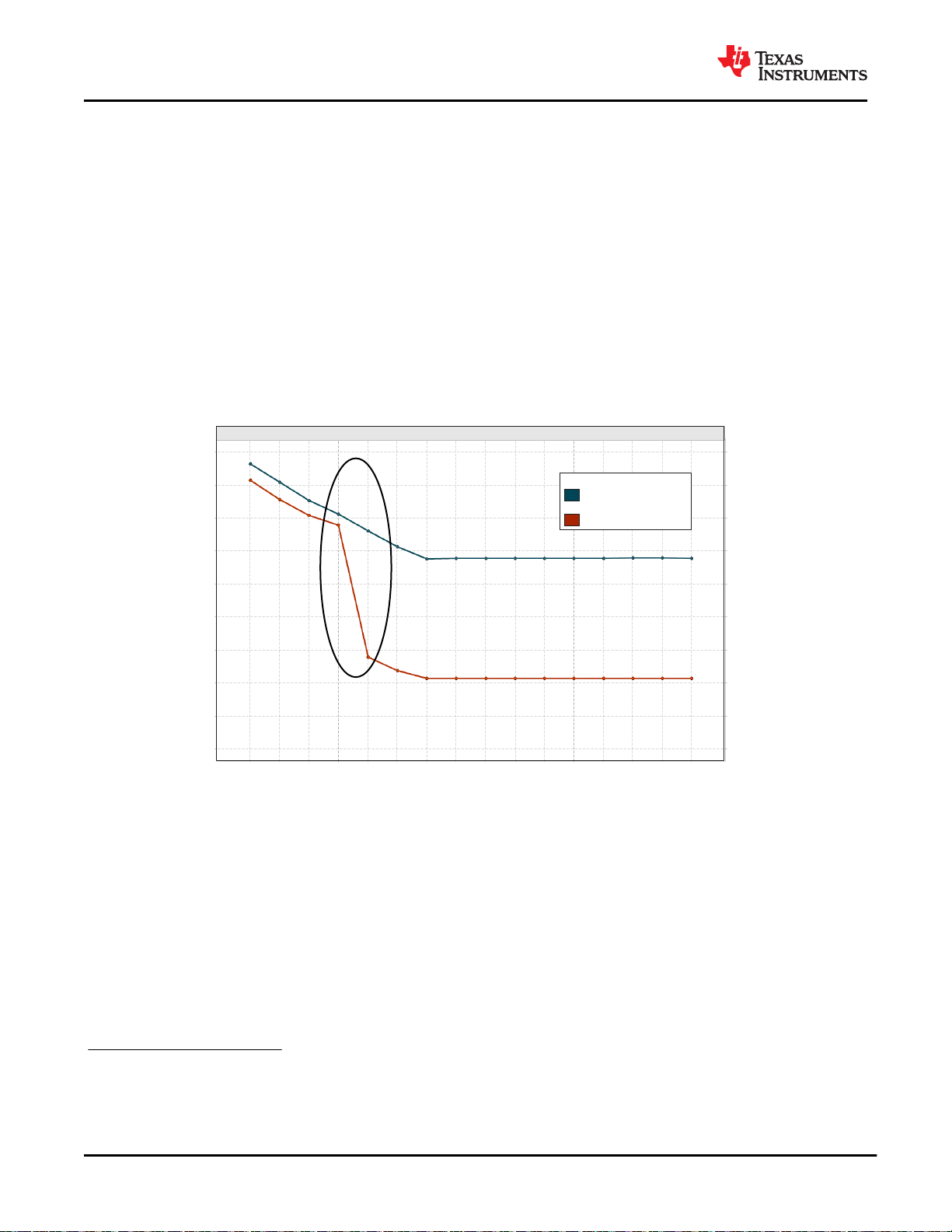
TX power level setting
TX Power (dBm)
19.00
17.00
15.00
13.00
11.00
9.00
7.00
5.00
3.00
1.00
0 1 2 3 4 5 6 7 8 9 10 11 12 13 14 15
280.00
264.40
249.00
233.30
218.00
202.00
186.70
171.00
155.60
140.00
1 DSSS
IBAT (VBAT @ 3.6 V)(mAmp)
Color by
TX Power (dBm)
IBAT (VBAT @ 3.6 V)
CC3235MODS, CC3235MODSF, CC3235MODAS, CC3235MODASF
SWRS243A – FEBRUARY 2020 – REVISED MAY 2020
www.ti.com
8.6 TX Power Control for 2.4 GHz Band
The CC3235MODS and CC3235MODAS has several options for modifying the output power of the device when
required. For the 2.4 GHz band it is possible to lower the overall output power at a global level using the global
TX power level setting. In addition, the 2.4 GHz band allows the user to enter additional back-offs 2, per channel,
region 3and modulation rates 4 5, through Image creator (see the Uniflash with Image Creator User Guide for
more details).
Figure 8-1, Figure 8-2, and Figure 8-3 show TX power and IBAT versus TX power level settings for the
CC3235MODS module at modulations of 1 DSSS, 6 OFDM, and 54 OFDM, respectively. For the
CC3235MODSF module, the IBAT current has an increase of approximately 10 mA to 15 mA depending on the
transmitted rate. The TX power level remains the same.
In Figure 8-1, the area enclosed in the circle represents a significant reduction in current during transition from
TX power level 3 to level 4. In the case of lower range requirements (14-dBm output power), TI recommends
using TX power level 4 to reduce the current.
5
Figure 8-1. TX Power and IBAT vs TX Power Level Settings (1 DSSS)
2
The back-off range is between –6 dB to +6 dB in 0.25-dB increments.
3
FCC, IC/ISED, ETSI/CE, MIC, and SRRC are supported.
4
Back-off rates are grouped into 11b rates, high modulation rates (MCS7, 54 OFDM and 48 OFDM), and
lower modulation rates (all other rates).
5
There will be a difference between the CC3135MOD and CC3135 IC TX power levels.
42 Submit Document Feedback
Product Folder Links: CC3235MODS CC3235MODSF CC3235MODAS CC3235MODASF
Copyright © 2020 Texas Instruments Incorporated

TX power level setting
TX Power (dBm)
19.00
17.00
15.00
13.00
11.00
9.00
7.00
5.00
3.00
1.00
0 1 2 3 4 5 6 7 8 9 10 11 12 13 14 15
IBAT (VBAT @ 3.6 V)(mAmp)
280.00
264.40
249.00
233.30
218.00
202.00
186.70
171.00
155.60
140.00
6 OFDM
Color by
TX Power (dBm)
IBAT (VBAT @ 3.6 V)
TX power level setting
TX Power (dBm)
19.00
17.00
15.00
13.00
11.00
9.00
7.00
5.00
3.00
1.00
0 1 2 3 4 5 6 7 8 9 10 11 12 13 14 15
54 OFDM
280.00
264.40
249.00
233.30
218.00
202.00
186.70
171.00
155.60
140.00
IBAT (VBAT @ 3.6 V)(mAmp)
Color by
TX Power (dBm)
IBAT (VBAT @ 3.6 V)
www.ti.com
CC3235MODS, CC3235MODSF, CC3235MODAS, CC3235MODASF
SWRS243A – FEBRUARY 2020 – REVISED MAY 2020
Figure 8-2. TX Power and IBAT vs TX Power Level Settings (6 OFDM)
Figure 8-3. TX Power and IBAT vs TX Power Level Settings (54 OFDM)
Copyright © 2020 Texas Instruments Incorporated
Product Folder Links: CC3235MODS CC3235MODSF CC3235MODAS CC3235MODASF
Submit Document Feedback
43

CC3235MODS, CC3235MODSF, CC3235MODAS, CC3235MODASF
SWRS243A – FEBRUARY 2020 – REVISED MAY 2020
www.ti.com
8.7 TX Power Control for 5 GHz
5-GHz power control is done via Image Creator where the maximum transmit power is provided 6. Within Image
Creator, power control is possible per channel, region 7, and modulation rate 8. In addition, it is possible to enter
an additional back-off 9factor per channel and modulation rate for further margin to regulatory requirements.
It is also possible to set the TX and RX trace losses to the antenna per band 10. The peak antenna gain 11can
also be provided, thus allowing further control. For a full description of options and capabilities see Uniflash with
Image Creator User Guide.
8.8 Brownout and Blackout Conditions
The module enters a brownout condition whenever the input voltage dips below V
BROWNOUT
(see Figure 8-4 and
Figure 8-5). This condition must be considered during design of the power supply routing, especially if operating
from a battery. High-current operations, such as a TX packet or any external activity (not necessarily related
directly to networking) can cause a drop in the supply voltage, potentially triggering a brownout. The resistance
includes the internal resistance of the battery, contact resistance of the battery holder (four contacts for a 2× AA
battery), and the wiring and PCB routing resistance.
Note
When the module is in HIBERNATE state, brownout is not detected. Only blackout is in effect during
HIBERNATE state.
6
The maximum transmit power range is 18 dBm to 0.125 dBm in 0.125-dBm decrements.
7
FCC, IC/ISED, ETSI/CE, MIC, and SRRC are supported.
8
Rates are grouped into high modulation rates (MCS7, 54 OFDM and 48 OFDM) and lower modulation rates
(all other rates).
9
The back-off range is 0 dBm to 18 dBm in 0.125-dBm increments, with the maximum back-off not exceed
that of the maximum transmit power.
10
The range of losses if from 0 dBm to 7.75 dBm in 0.125-dBm increments.
11
The antenna gain has a range of -2 dBi to 5.75 dBi in 0.125-dBi increments.
44 Submit Document Feedback
Product Folder Links: CC3235MODS CC3235MODSF CC3235MODAS CC3235MODASF
Copyright © 2020 Texas Instruments Incorporated

www.ti.com
CC3235MODS, CC3235MODSF, CC3235MODAS, CC3235MODASF
SWRS243A – FEBRUARY 2020 – REVISED MAY 2020
Figure 8-4. Brownout and Blackout Levels (1 of 2)
Figure 8-5. Brownout and Blackout Levels (2 of 2)
In the brownout condition, all sections of the device shut down within the module except for the Hibernate block
(including the 32-kHz RTC clock), which remains on. The current in this state can reach approximately 400 µA.
The blackout condition is equivalent to a hardware reset event in which all states within the module are lost.
V
brownout
= 2.1 V and V
blackout
= 1.67 V
Table 8-5 lists the brownout and blackout voltage levels.
Table 8-5. Brownout and Blackout Voltage Levels
CONDITION VOLTAGE LEVEL UNIT
V
brownout
V
blackout
Copyright © 2020 Texas Instruments Incorporated
Product Folder Links: CC3235MODS CC3235MODSF CC3235MODAS CC3235MODASF
2.1 V
1.67 V
Submit Document Feedback
45

CC3235MODS, CC3235MODSF, CC3235MODAS, CC3235MODASF
SWRS243A – FEBRUARY 2020 – REVISED MAY 2020
8.9 Electrical Characteristics for GPIO Pins
Table 8-6. GPIO Pins Except 25, 26, 42, and 44 (25°C)
TA = 25°C, V
C
Pin capacitance 4 pF
IN
V
High-level input voltage 0.65 × V
IH
V
Low-level input voltage –0.5 0.35 × V
IL
I
High-level input current 5 nA
IH
I
Low-level input current 5 nA
IL
V
High-level output voltage
OH
V
Low-level output voltage
OL
High-level
I
OH
source current,
Low-level sink
I
OL
current,
= 3.3 V
BAT
PARAMETER TEST CONDITIONS MIN NOM MAX UNIT
IL = 2 mA; configured I/O drive
strength = 2 mA;
2.4 V ≤ VDD < 3.6 V
IL = 4 mA; configured I/O drive
strength = 4 mA;
2.4 V ≤ VDD < 3.6 V
IL = 6 mA; configured I/O drive
strength = 6 mA;
2.4 V ≤ VDD < 3.6 V
IL = 2 mA; configured I/O drive
strength = 2 mA;
2.3 V ≤ VDD < 2.4 V
IL = 2 mA; configured I/O drive
strength = 2 mA;
2.4 V ≤ VDD < 3.6 V
IL = 4 mA; configured I/O drive
strength = 4 mA;
2.4 V ≤ VDD < 3.6 V
IL = 6 mA; configured I/O drive
strength = 6 mA;
2.4 V ≤ VDD < 3.6 V
IL = 2 mA; configured I/O drive
strength = 2 mA;
2.3 V ≤ VDD < 2.4 V
2-mA drive 2
6-mA drive 6
2-mA drive 2
6-mA drive 6
DD
VDD × 0.2
VDD × 0.2
VDD × 0.2
VDD × 0.25
(1)
VDD + 0.5 V V
VDD × 0.8
VDD × 0.7
VDD × 0.7
VDD × 0.75
DD
www.ti.com
V
V
V
mA4-mA drive 4
mA4-mA drive 4
(1) TI recommends using the lowest possible drive strength that is adequate for the applications. This recommendation minimizes the risk
of interference to the WLAN radio and reduces any potential degradation of RF sensitivity and performance. The default drive strength
setting is 6 mA.
46 Submit Document Feedback
Product Folder Links: CC3235MODS CC3235MODSF CC3235MODAS CC3235MODASF
Copyright © 2020 Texas Instruments Incorporated
www.ti.com
Table 8-7. GPIO Pins 25, 26, 42, and 44 (25°C)
PARAMETER TEST CONDITIONS MIN NOM MAX UNIT
CINPin capacitance 7 pF
VIHHigh-level input voltage 0.65 × V
VILLow-level input voltage –0.5 0.35 × V
I
High-level input current 50 nA
IH
I
Low-level input current 50 nA
IL
IL = 2 mA; configured I/O drive
strength = 2 mA;
2.4 V ≤ VDD < 3.6 V
IL = 4 mA; configured I/O drive
strength = 4 mA;
VOHHigh-level output voltage
VOLLow-level output voltage
2-mA drive 1.5
High-level source
I
OH
current, VOH = 2.4
6-mA drive 3.5
2-mA drive 1.5
Low-level sink
I
OL
current,
6-mA drive 3.5
VILnRESET 0.6 V
2.4 V ≤ VDD < 3.6 V
IL = 6 mA; configured I/O drive
strength = 6 mA;
2.4 V ≤ VDD < 3.6 V
IL = 2 mA; configured I/O drive
strength = 2 mA;
2.3 V ≤ VDD < 2.4 V
IL = 2 mA; configured I/O drive
strength = 2 mA;
2.4 V ≤ VDD < 3.6 V
IL = 4 mA; configured I/O drive
strength = 4 mA;
2.4 V ≤ VDD < 3.6 V
IL = 6 mA; configured I/O drive
strength = 6 mA;
2.4 V ≤ VDD < 3.6 V
IL = 2 mA; configured I/O drive
strength = 2 mA;
2.3 V ≤ VDD < 2.4 V
SWRS243A – FEBRUARY 2020 – REVISED MAY 2020
(1)
DD
VDD + 0.5 V V
DD
VDD × 0.8
VDD × 0.7
VDD × 0.7
VDD × 0.75
VDD × 0.2
VDD × 0.2
VDD × 0.2
VDD × 0.25
CC3235MODS, CC3235MODSF, CC3235MODAS, CC3235MODASF
V
V
V
mA4-mA drive 2.5
mA4-mA drive 2.5
(1) TI recommends using the lowest possible drive strength that is adequate for the applications. This recommendation minimizes the risk
of interference to the WLAN radio and reduces any potential degradation of RF sensitivity and performance. The default drive strength
setting is 6 mA.
8.9.1 Electrical Characteristics for Pin Internal Pullup and Pulldown (25°C)
PARAMETER
I
OH
I
OL
Copyright © 2020 Texas Instruments Incorporated
Pullup current
(VDD = 3.0 V)
Pulldown current
(VDD = 3.0 V)
Product Folder Links: CC3235MODS CC3235MODSF CC3235MODAS CC3235MODASF
TEST CONDITIONS MIN NOM MAX UNIT
10 µA
10 µA
Submit Document Feedback
47

CC3235MODS, CC3235MODSF, CC3235MODAS, CC3235MODASF
SWRS243A – FEBRUARY 2020 – REVISED MAY 2020
8.10 CC3235MODAx Antenna Characteristics
TA = 25°C
PARAMETER TEST CONDITIONS MIN TYP MAX UNIT
Polarization Linear
Peak Gain
Efficiency
2.4 GHz Band 3.5 dBi
5 GHz Band 4.5 dBi
2.4 GHz Band 70%
5 GHz Band 65%
8.11 WLAN Receiver Characteristics
Table 8-8. WLAN Receiver Characteristics: 2.4 GHz Band
TA = 25°C, V
Sensitivity
(8% PER for 11b rates, 10% PER for 11g/11n
(1)
rates)
Maximum input level
(10% PER)
= 2.3 V to 3.6 V. Parameters are measured at the SoC pin on channel 6 (2437 MHz).
BAT
PARAMETER TEST CONDITIONS (Mbps) MIN TYP MAX UNIT
1 DSSS –94.5
2 DSSS –92.5
11 CCK –86.5
6 OFDM –89
9 OFDM –88.5
18 OFDM –85
36 OFDM –79
54 OFDM –73
MCS7 (GF)
802.11b –2.5
802.11g –8.5
(2)
–70
www.ti.com
dBm
dBm
(1) Sensitivity is 1-dB worse on channel 13 (2472 MHz).
(2) Sensitivity for mixed mode is 1-dB worse.
Table 8-9. WLAN Receiver Characteristics: 5 GHz Band
TA = 25°C, V
Sensitivity
(10% PER for 11g/11n rates)
Maximum input level 802.11a -17 dBm
(1) Sensitivity for mixed mode is 1-dB worse.
= 2.3 V to 3.6 V.
BAT
PARAMETER TEST CONDITIONS (Mbps) MIN TYP MAX UNIT
6 OFDM -89
9 OFDM -88
18 OFDM -85
36 OFDM -78.5
54 OFDM -72
MCS7 (GF)
(1)
-68
dBm
48 Submit Document Feedback
Product Folder Links: CC3235MODS CC3235MODSF CC3235MODAS CC3235MODASF
Copyright © 2020 Texas Instruments Incorporated

www.ti.com
SWRS243A – FEBRUARY 2020 – REVISED MAY 2020
8.12 WLAN Transmitter Characteristics
Table 8-10. WLAN Transmitter Characteristics: 2.4 GHz Band
CC3235MODS, CC3235MODSF, CC3235MODAS, CC3235MODASF
TA = 25°C, V
Operating frequency range
Maximum RMS output power measured at 1
dB from IEEE spectral mask or EVM
Transmit center frequency accuracy –25 25 ppm
= 2.3 V to 3.6 V.
BAT
PARAMETER TEST CONDITIONS MIN TYP MAX UNIT
(4) (5)
(1)
Parameters measured at SoC pin on channel 6 (2437 MHz).
2412 2472 MHz
1 DSSS 16
2 DSSS 16
11 CCK 16.3
6 OFDM 15.3
9 OFDM 15.3
18 OFDM 15
36 OFDM 14
54 OFDM 12.5
MCS7 11
(2) (3)
dBm
(1) Transmit power will be reduced by 1.5dB for V
(2) The 11g/n low rates on edge channels (2412 and 2462 MHz) have reduced TX power to meet FCC emission limits.
(3) Power of 802.11b rates are reduced to meet ETSI requirements in Europe.
(4) Channels 1 (2142 MHz) through 11 (2462 MHz) are supported for FCC.
(5) Channels 1 (2142 MHz) through 13 (2472MHz) are supported for Europe and Japan. Note that channel 14 is not supported for Japan.
BAT
< 2.8V
Table 8-11. WLAN Transmitter Characteristics: 5 GHz Band
TA = 25°C, V
and 157 .
Operating frequency range
Maximum RMS output power measured at 1
dB from IEEE spectral mask or EVM
Transmit center frequency accuracy -20 20 ppm
(1) Transmit power will be reduced by 1.5dB for V
(2) FCC band covers U-NII-1, U-NII-2A, U-NII-2C, and U-NII-3 20-MHz BW modulations.
(3) Europe bands 1, 2 and 3, 20-MHz BW modulations are supported.
(4) For Japan, W52, W53 and W56, 20-MHz BW modulations are supported.
(5) FCC channels 36, 60, 64, 100, and 140, where harmonics/sub-harmonics of fall in the FCC restricted band, have reduced output
power to meet the FCC RSE requirement.
(6) The edge channels (100 and 140) have reduced TX power to meet FCC emissions limits.
= 2.3 V to 3.6 V.
BAT
(5) (6)
PARAMETER TEST CONDITIONS MIN TYP MAX UNIT
(2) (3) (4)
(1)
Parameters measured at SoC pin are the average of channels 40, 56, 120,
5180 5825 MHz
6 OFDM 15.1
9 OFDM 15.1
18 OFDM 15.1
36 OFDM 13.6
54 OFDM 12
MCS7 11
< 2.8V
BAT
dBm
Copyright © 2020 Texas Instruments Incorporated
Product Folder Links: CC3235MODS CC3235MODSF CC3235MODAS CC3235MODASF
Submit Document Feedback
49

CC3235MODS, CC3235MODSF, CC3235MODAS, CC3235MODASF
SWRS243A – FEBRUARY 2020 – REVISED MAY 2020
www.ti.com
8.13 BLE and WLAN Coexistence Requirements
For proper BLE and WLAN 2.4 GHz radio coexistence, the following requirements must be met:
Table 8-12. BLE/WLAN Coex
PARAMETER Band MIN TYP MAX UNIT
Port-to-port isolation Dual antenna configuration
(1) The CC3235MODS and CC3235MODAS modules are compatible with TI BLE modules using an external RF switch.
(2) A single antenna configuration is possible using the CC3x35 devices.
(3) For dual antenna configuration, the antenna placement must be such that isolation between the BLE and WLAN ports is at least 20 dB.
(1)
Isolation Requirement
(2)
20
(3)
dB
8.14 Reset Requirement
PARAMETER MIN TYP MAX UNIT
V
IH
V
IL
Tr and T
(1) The nRESET pin must be held below 0.6 V for the module to register a reset.
Operation mode level 0.65 × V
Shutdown mode level
(1)
0 0.6 V
BAT
Minimum time for nReset low for resetting the module 5 ms
Rise and fall times 20 µs
f
V
8.15 Thermal Resistance Characteristics for MOB and MON Packages
NO.
PARAMETER DESCRIPTION °C/W
T1 RΘ
T2 RΘ
JC
JB
T3
T4
T5 13.4 2
RΘ
JA
Junction-to-case 11.4 N/A
Junction-to-board 8.0 N/A
Junction-to-free air 19.1 0
Junction-to-moving air
T6 12.5 3
T7
T8
T9 6.1 2
Ψ
JT
Junction-to-free air 5.4 0
Junction-to-package top
T10 6.5 3
T11
T12
T13 6.6 2
Ψ
JB
Junction-to-free air 6.8 0
Junction-to-board
T14 6.5 3
(1) °C/W = degrees Celsius per watt.
(2) These values are based on a JEDEC-defined 2S2P system (with the exception of the Theta JC [RΘJC] value, which is based on a
JEDEC-defined 1S0P system) and will change based on environment as well as application. For more information, see these EIA/
JEDEC standards:
• JESD51-2, Integrated Circuits Thermal Test Method Environmental Conditions - Natural Convection (Still Air)
• JESD51-3, Low Effective Thermal Conductivity Test Board for Leaded Surface Mount Packages
• JESD51-7, High Effective Thermal Conductivity Test Board for Leaded Surface Mount Packages
• JESD51-9, Test Boards for Area Array Surface Mount Package Thermal Measurements
Power dissipation of 2 W and an ambient temperature of 70°C is assumed.
(3) m/s = meters per second.
(1) (2)
AIR FLOW (m/s)
14.7 1
5.8 1
6.6 1
(3)
50 Submit Document Feedback
Product Folder Links: CC3235MODS CC3235MODSF CC3235MODAS CC3235MODASF
Copyright © 2020 Texas Instruments Incorporated

POWER
OFF
HW INIT FW INIT
APP CODE
EXECUTION
VBAT
nRESET
STATE
T1 T2 T3
RESET
T4
32-kHz
RTC CLK
APP CODE
LOAD
www.ti.com
SWRS243A – FEBRUARY 2020 – REVISED MAY 2020
8.16 Timing and Switching Characteristics
8.16.1 Power-Up Sequencing
For proper start-up of the CC3235MODx and CC3235MODAx module, perform the recommended power-up
sequencing as follows:
CC3235MODS, CC3235MODSF, CC3235MODAS, CC3235MODASF
1. Tie V
(pin 37) and V
BAT1
(pin 40) together on the board.
BAT2
2. Hold the nRESET pin low while the supplies are ramping up.
Figure 8-6 shows the reset timing diagram for the first-time power-up and reset removal.
Figure 8-6. First-Time Power-Up and Reset Removal Timing Diagram
Table 8-13 lists the timing requirements for the first-time power-up and reset removal.
Table 8-13. First-Time Power-Up and Reset Removal Timing Requirements
ITEM NAME DESCRIPTION MIN TYP MAX UNIT
T1 nReset time nReset timing after VBAT supplies are stable 1 ms
T2 Hardware wake-up time 25 ms
Time taken by ROM
T3
firmware to initialize
hardware
App code load time for
CC3235MODS and
CC3235MODAS
T4
App code load time for
CC3235MODSF and
CC3235MODASF
Includes internal 32-kHz XOSC settling time 1.1 s
CC3235MODS and CC3235MODAS Image size (KB) × 1.7 ms
CC3235MODSF and CC3235MODASF Image size (KB) × 0.06 ms
8.16.2 Power-Down Sequencing
For proper power down of the CC3235MODx and CC3235MODAx module, ensure that the nRESET (pin 35) and
nHIB (pin 4) pins have remained in a known state for a minimum of 200 ms before removing power from the
module.
8.16.3 Device Reset
When a device restart is required, issue a negative pulse to the nRESET pin. Ensure the reset is properly
applied: A negative reset pulse (on pin 35) of at least 200-mS duration.
Copyright © 2020 Texas Instruments Incorporated
Product Folder Links: CC3235MODS CC3235MODSF CC3235MODAS CC3235MODASF
Submit Document Feedback
51

Hibernate
HW WAKEUP FW INIT
APP CODE
LOAD
EXECUTION
ACTIVE
Application software requests
entry to hibernate moade
VBAT
nRESET
STATE
32-kHz
RTC CLK
T
HIB_MIN
T
wake_from_hib
T
APP_CODE_LOAD
CC3235MODS, CC3235MODSF, CC3235MODAS, CC3235MODASF
SWRS243A – FEBRUARY 2020 – REVISED MAY 2020
8.16.4 Wake Up From Hibernate Timing
Table 8-14 lists the software hibernate timing requirements.
Note
The internal 32.768-kHz crystal is kept enabled by default when the module goes to hibernate.
Table 8-14. Software Hibernate Timing Requirements
ITEM NAME DESCRIPTION MIN TYP MAX UNIT
T
HIB_MIN
T
wake_from_hib
(1)
T_APP_CODE_LOAD
Minimum hibernate time 10 ms
Hardware wakeup time plus
firmware initialization time
App code load time for
CC3235MODS and
CC3235MODS and CC3235MODAS Image size (KB) × 1.7 ms
CC3235MODAS
App code load time for
CC3235MODSF and
CC3235MODASF
CC3235MODSF and
CC3235MODASF
Image size (KB) × 0.06 ms
50
www.ti.com
(2)
ms
(1) T
wake_from_hib
can be 200 ms on rare occasions when calibration is performed. Calibration is performed sparingly, typically when exiting
Hibernate and only if temperature has changed by more than 20°C or more than 24 hours have elapsed since a prior calibration.
(2) Wake-up time can extend to 75 ms if a patch is downloaded from the serial flash.
Figure 8-7 shows the timing diagram for wake up from the hibernate state.
52 Submit Document Feedback
Figure 8-7. Wake Up From Hibernate Timing Diagram
Product Folder Links: CC3235MODS CC3235MODSF CC3235MODAS CC3235MODASF
Copyright © 2020 Texas Instruments Incorporated

T2
T6 T7
T9
CLK
MISO
MOSI
T8
www.ti.com
SWRS243A – FEBRUARY 2020 – REVISED MAY 2020
8.16.5 Peripherals Timing
This section describes the peripherals that are supported by the CC3235MODx and CC3235MODAx module, as
follows:
• SPI
• I2S
• GPIOs
• I2C
• IEEE 1149.1 JTAG
• ADC
• Camera parallel port
• External flash
• UART
• SD Host
• Timers
8.16.5.1 SPI
CC3235MODS, CC3235MODSF, CC3235MODAS, CC3235MODASF
8.16.5.1.1 SPI Master
The CC3235MODx and CC3235MODAx MCU includes one SPI module, which can be configured as a master or
slave device. The SPI includes a serial clock with programmable frequency, polarity, and phase; a programmable
timing control between chip select and external clock generation; and a programmable delay before the first SPI
word is transmitted. Slave mode does not include a dead cycle between two successive words.
Figure 8-8 shows the timing diagram for the SPI master.
Figure 8-8. SPI Master Timing Diagram
Table 8-15 lists the timing parameters for the SPI master.
Table 8-15. SPI Master Timing Parameters
ITEM NAME DESCRIPTION MIN MAX UNIT
(1)
F
T2 T
T6 tIS
T7 tIH
T8 tOD
T9 tOH
clk
D
(1)
(1)
(1)
(1)
(1)
(1)
Clock frequency 20 MHz
Clock period 50 ns
Duty cycle 45% 55%
RX data setup time 1 ns
RX data hold time 2 ns
TX data output delay 8.5 ns
TX data hold time 8 ns
(1) Timing parameter assumes a maximum load of 20 pF.
Copyright © 2020 Texas Instruments Incorporated
Product Folder Links: CC3235MODS CC3235MODSF CC3235MODAS CC3235MODASF
Submit Document Feedback
53

T2
T6 T7
T9
CLK
MISO
MOSI
T8
CC3235MODS, CC3235MODSF, CC3235MODAS, CC3235MODASF
SWRS243A – FEBRUARY 2020 – REVISED MAY 2020
8.16.5.1.2 SPI Slave
Figure 8-9 shows the timing diagram for the SPI slave.
Figure 8-9. SPI Slave Timing Diagram
Table 8-16 lists the timing parameters for the SPI slave.
Table 8-16. SPI Slave Timing Parameters
ITEM NAME DESCRIPTION MIN MAX UNIT
(1)
F
T2 T
clk
D
T6 tIS
T7 tIH
T8 tOD
T9 tOH
(1)
(1)
(1)
(1)
(1)
(1)
Clock frequency @ VBAT = 3.3 V 20
Clock frequency @ VBAT ≤ 2.3 V 12
Clock period 50 ns
Duty cycle 45% 55%
RX data setup time 4 ns
RX data hold time 4 ns
TX data output delay 20 ns
TX data hold time 24 ns
www.ti.com
MHz
(1) Timing parameter assumes a maximum load of 20 pF at 3.3 V.
54 Submit Document Feedback
Product Folder Links: CC3235MODS CC3235MODSF CC3235MODAS CC3235MODASF
Copyright © 2020 Texas Instruments Incorporated

T2 T1 T3
T4
McACLKX
McAFSX
McAXR0/1
T4
T2 T1 T3
T4
McACLKX
McAFSX
McAXR0/1
T5
www.ti.com
SWRS243A – FEBRUARY 2020 – REVISED MAY 2020
8.16.5.2 I2S
The McASP interface functions as a general-purpose audio serial port optimized for multichannel audio
applications and supports transfer of two stereo channels over two data pins. The McASP consists of transmit
and receive sections that operate synchronously and have programmable clock and frame-sync polarity. A
fractional divider is available for bit-clock generation.
CC3235MODS, CC3235MODSF, CC3235MODAS, CC3235MODASF
8.16.5.2.1 I2S Transmit Mode
Figure 8-10 shows the timing diagram for the I2S transmit mode.
Figure 8-10. I2S Transmit Mode Timing Diagram
Table 8-17 lists the timing parameters for the I2S transmit mode.
Table 8-17. I2S Transmit Mode Timing Parameters
ITEM NAME DESCRIPTION MIN MAX UNIT
T1 f
T2 tLP
T3 tHT
T4 tOH
(1)
clk
(1)
(1)
(1)
Clock frequency 9.216 MHz
Clock low period 1/2 fclk ns
Clock high period 1/2 fclk ns
TX data hold time 22 ns
(1) Timing parameter assumes a maximum load of 20 pF.
8.16.5.2.2 I2S Receive Mode
Figure 8-11 shows the timing diagram for the I2S receive mode.
Figure 8-11. I2S Receive Mode Timing Diagram
Table 8-18 lists the timing parameters for the I2S receive mode.
Table 8-18. I2S Receive Mode Timing Parameters
ITEM NAME DESCRIPTION MIN MAX UNIT
T1 f
T2 tLP
T3 tHT
T4 tOH
T5 tOS
(1) Timing parameter assumes a maximum load of 20 pF.
(1)
clk
(1)
(1)
(1)
(1)
Clock frequency 9.216 MHz
Clock low period 1/2 f
Clock high period 1/2 f
RX data hold time 0 ns
RX data setup time 15 ns
clk
clk
ns
ns
Copyright © 2020 Texas Instruments Incorporated
Product Folder Links: CC3235MODS CC3235MODSF CC3235MODAS CC3235MODASF
Submit Document Feedback
55

SWAS031-067
V
DD
80%
20%
t
GPIOF
t
GPIOR
CC3235MODS, CC3235MODSF, CC3235MODAS, CC3235MODASF
SWRS243A – FEBRUARY 2020 – REVISED MAY 2020
www.ti.com
8.16.5.3 GPIOs
All digital pins of the module can be used as general-purpose input/output (GPIO) pins. The GPIO module
consists of four GPIO blocks, each of which provides eight GPIOs. The GPIO module supports 24
programmable GPIO pins, depending on the peripheral used. Each GPIO has configurable pullup and pulldown
strength (weak 10 µA), configurable drive strength (2, 4, and 6 mA), and open-drain enable.
Figure 8-12 shows the GPIO timing diagram.
Figure 8-12. GPIO Timing Diagram
Table 8-19 lists the GPIO output transition times for V
Table 8-19. GPIO Output Transition Times (V
DRIVE
STRENGTH (mA)
2
4
6
(1) V
(2) The transition data applies to the pins other than the multiplexed analog-digital pins 25, 26, 42, and 44.
= 2.3 V, T = 25°C, total pin load = 30 pF
BAT
DRIVE STRENGTH
CONTROL BITS
2MA_EN=1
4MA_EN=0
2MA_EN=0
4MA_EN=1
2MA_EN=1
4MA_EN=1
MIN NOM MAX MIN NOM MAX
11.7 13.9 16.3 11.5 13.9 16.7 ns
13.7 15.6 18.0 9.9 11.6 13.6 ns
5.5 6.4 7.4 3.8 4.7 5.8 ns
BAT
T
r
= 2.3 V.
= 2.3 V)
BAT
(1) (2)
Table 8-20 lists the GPIO output transition times for V
Table 8-20. GPIO Output Transition Times (V
DRIVE
STRENGTH (mA)
2
4
6
DRIVE STRENGTH
CONTROL BITS
2MA_EN=1
4MA_EN=0
2MA_EN=0
4MA_EN=1
2MA_EN=1
4MA_EN=1
MIN NOM MAX MIN NOM MAX
8.0 9.3 10.7 8.2 9.5 11.0 ns
6.6 7.1 7.6 4.7 5.2 5.8 ns
3.2 3.5 3.7 2.3 2.6 2.9 ns
BAT
T
r
= 3.3 V.
= 3.3 V)
BAT
(1) (2)
T
f
T
f
UNIT
UNIT
(1) V
(2) The transition data applies to the pins except the multiplexed analog-digital pins 29, 30, 45, 50, 52 and 53.
56 Submit Document Feedback
= 3.3 V, T = 25°C, total pin load = 30 pF
BAT
Product Folder Links: CC3235MODS CC3235MODSF CC3235MODAS CC3235MODASF
Copyright © 2020 Texas Instruments Incorporated

T2 T6
T5
T9
T3T8
T7
T4
T1
I2CSCL
www.ti.com
SWRS243A – FEBRUARY 2020 – REVISED MAY 2020
8.16.5.3.1 GPIO Input Transition Time Parameters
Table 8-21 lists the input transition time parameters.
Table 8-21. GPIO Input Transition Time Parameters
CC3235MODS, CC3235MODSF, CC3235MODAS, CC3235MODASF
MIN MAX UNIT
t
r
t
f
Input transition time (tr, tf), 10% to 90%
1 3 ns
1 3 ns
8.16.5.4 I2C
The CC3235MODx and CC3235MODAx MCU includes one I2C module operating with standard (100 kbps) or
fast (400 kbps) transmission speeds.
Figure 8-13 shows the I2C timing diagram.
Figure 8-13. I2C Timing Diagram
Table 8-22 lists the I2C timing parameters.
Table 8-22. I2C Timing Parameters
ITEM NAME DESCRIPTION MIN MAX UNIT
T2 t
T3 t
T4 t
T5 t
T6 t
T7 t
T8 t
T9 t
LP
SRT
DH
SFT
HT
DS
SCSR
SCS
(1) This value depends on the value programmed in the clock period register of I2C. Maximum output frequency is the result of the minimal
value programmed in this register.
(2) Because I2C is an open-drain interface, the controller can drive logic 0 only. Logic is the result of external pullup. Rise time depends on
the value of the external signal capacitance and external pullup register.
(3) All timing is with 6-mA drive and 20-pF load.
Clock low period See
SCL/SDA rise time See
Data hold time NA
SCL/SDA fall time 3 ns
Clock high time See
Data setup time tLP/2 System clock
Start condition setup time 36 System clock
Stop condition setup time 24 System clock
(3)
(1)
(1)
System clock
(2)
System clock
ns
Copyright © 2020 Texas Instruments Incorporated
Product Folder Links: CC3235MODS CC3235MODSF CC3235MODAS CC3235MODASF
Submit Document Feedback
57

T2 T3
T4
T7 T8
T7
T8
T9 T10 T9 T10
T1
T11
TDI Input Valid
TDO Output Valid
TDO Output Valid
TMS Input Valid
TDI Input Valid
TCK
TDI
TMS Input Valid
CC3235MODS, CC3235MODSF, CC3235MODAS, CC3235MODASF
SWRS243A – FEBRUARY 2020 – REVISED MAY 2020
www.ti.com
8.16.5.5 IEEE 1149.1 JTAG
The Joint Test Action Group (JTAG) port is an IEEE standard that defines a test access port (TAP) and boundary
scan architecture for digital integrated circuits and provides a standardized serial interface to control the
associated test logic. For detailed information on the operation of the JTAG port and TAP controller, see the
IEEE Standard 1149.1,Test Access Port and Boundary-Scan Architecture.
Figure 8-14 shows the JTAG timing diagram.
Figure 8-14. JTAG Timing Diagram
Table 8-23 lists the JTAG timing parameters.
Table 8-23. JTAG Timing Parameters
ITEM NAME DESCRIPTION MIN MAX UNIT
T1 f
T2 t
T3 t
T4 t
T7 t
T8 t
T9 t
T10 t
T11 t
TCK
TCK
CL
CH
TMS_SU
TMS_HO
TDI_SU
TDI_HO
TDO_HO
Clock frequency 15 MHz
Clock period 1 / f
Clock low period t
Clock high period t
TCK
TCK
TMS setup time 1 ns
TMS hold time 16 ns
TDI setup time 1 ns
TDI hold time 16 ns
TDO hold time 15 ns
TCK
/ 2 ns
/ 2 ns
ns
58 Submit Document Feedback
Product Folder Links: CC3235MODS CC3235MODSF CC3235MODAS CC3235MODASF
Copyright © 2020 Texas Instruments Incorporated

2 µs 2 µs 2 µs 2 µs 2 µs 2 µs 2 µs 2 µs 2 µs 2 µs
Repeats Every 16 µs
ADC CLOCK
= 10 MHz
Sampling
4 cycles
SAR Conversion
16 cycles
Sampling
4 cycles
SAR Conversion
16 cycles
Sampling
4 cycles
SAR Conversion
16 cycles
Sampling
4 cycles
SAR Conversion
16 cycles
EXT CHANNEL 0
INTERNAL CHANNEL
EXT CHANNEL 1
INTERNAL CHANNEL
Internal Ch
www.ti.com
SWRS243A – FEBRUARY 2020 – REVISED MAY 2020
8.16.5.6 ADC
Table 8-24 lists the ADC electrical specifications. See CC32xx ADC Appnote for further information on using the
ADC and for application-specific examples.
Figure 8-15. ADC Clock Timing Diagram
Figure 8-15 shows the ADC clock timing diagram.
Table 8-24. ADC Electrical Specifications
CC3235MODS, CC3235MODSF, CC3235MODAS, CC3235MODASF
PARAMETER DESCRIPTION
Nbits Number of bits 12 Bits
INL Integral nonlinearity
DNL Differential nonlinearity
Input range 0 1.4 V
Driving source
impedance
FCLK Clock rate
Input capacitance 12 pF
Input impedance
Number of channels 4
F
sample
Sampling rate of each pin 62.5 KSPS
F_input_max Maximum input signal frequency 31 kHz
SINAD Signal-to-noise and distortion
I_active Active supply current
I_PD
Absolute offset error FCLK = 10 MHz ±2 mV
Power-down supply current for
core supply
Gain error ±2%
TEST CONDITIONS /
ASSUMPTIONS
MIN TYP MAX UNIT
Worst-case deviation from
histogram method over full scale
(not including first and last three
–2.5 2.5 LSB
LSB levels)
Worst-case deviation of any step
from ideal
Successive approximation input
clock rate
–1 4 LSB
10 MHz
ADC Pin 57 2.15
ADC Pin 58 0.7
ADC Pin 59 2.12
ADC Pin 60 1.17
Input frequency DC to 300 Hz
and 1.4 Vpp sine wave input
55 60 dB
Average for analog-to-digital
during conversion without
1.5 mA
reference current
Total for analog-to-digital when
not active (this must be the SoC
level test)
100 Ω
kΩ
1 µA
Copyright © 2020 Texas Instruments Incorporated
Product Folder Links: CC3235MODS CC3235MODSF CC3235MODAS CC3235MODASF
Submit Document Feedback
59

CC3235MODS, CC3235MODSF, CC3235MODAS, CC3235MODASF
SWRS243A – FEBRUARY 2020 – REVISED MAY 2020
Table 8-24. ADC Electrical Specifications (continued)
PARAMETER DESCRIPTION
V
ref
ADC reference voltage 1.467 V
TEST CONDITIONS /
ASSUMPTIONS
www.ti.com
MIN TYP MAX UNIT
60 Submit Document Feedback
Product Folder Links: CC3235MODS CC3235MODSF CC3235MODAS CC3235MODASF
Copyright © 2020 Texas Instruments Incorporated
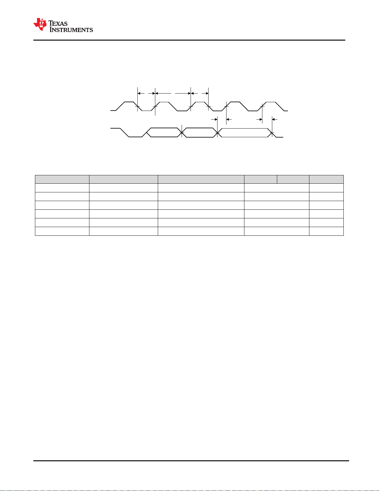
pCLK
pDATA
T3 T2 T4
T6
T7
www.ti.com
SWRS243A – FEBRUARY 2020 – REVISED MAY 2020
8.16.5.7 Camera Parallel Port
The fast camera parallel port interfaces with a variety of external image sensors, stores the image data in a
FIFO, and generates DMA requests. The camera parallel port supports 8 bits.
Figure 8-16 shows the timing diagram for the camera parallel port.
Figure 8-16. Camera Parallel Port Timing Diagram
Table 8-25 lists the timing parameters for the camera parallel port.
Table 8-25. Camera Parallel Port Timing Parameters
ITEM NAME DESCRIPTION MIN MAX UNIT
pCLK Clock frequency 2 MHz
CC3235MODS, CC3235MODSF, CC3235MODAS, CC3235MODASF
T2 T
T3 t
T4 t
T6 t
T7 t
clk
LP
HT
IS
IH
Clock period 1/pCLK ns
Clock low period T
Clock high period T
RX data setup time 2 ns
RX data hold time 2 ns
/2 ns
clk
/2 ns
clk
8.16.5.8 UART
The CC3235MODx and CC3235MODAx MCU includes two UARTs with the following features:
• Programmable baud-rate generator allowing speeds up to 3 Mbps
• Separate 16-bit × 8-bit TX and RX FIFOs to reduce CPU interrupt service loading
• Programmable FIFO length, including a 1-byte-deep operation providing conventional double-buffered
interface
• FIFO trigger levels of 1/8, 1/4, 1/2, 3/4, and 7/8
• Standard asynchronous communication bits for start, stop, and parity
• Generation and detection of line-breaks
• Fully programmable serial interface characteristics:
– 5, 6, 7, or 8 data bits
– Generation and detection of even, odd, stick, or no-parity bits
– Generation of 1 or 2 stop-bits
• RTS and CTS hardware flow support
• Standard FIFO-level and end-of-transmission interrupts
• Efficient transfers using µDMA:
– Separate channels for transmit and receive
– Receive single request asserted when data is in the FIFO; burst request asserted at programmed FIFO
level
– Transmit single request asserted when there is space in the FIFO; burst request asserted at programmed
FIFO level
• System clock is used to generate the baud clock.
Copyright © 2020 Texas Instruments Incorporated
Product Folder Links: CC3235MODS CC3235MODSF CC3235MODAS CC3235MODASF
Submit Document Feedback
61

CC3235MODS, CC3235MODSF, CC3235MODAS, CC3235MODASF
SWRS243A – FEBRUARY 2020 – REVISED MAY 2020
www.ti.com
8.16.5.9 External Flash Interface
The CC3235MODx and CC3235MODAx MCU includes the Macronix™ 32-Mbit serial flash. The serial flash can
be programmed directly using the external flash interface (pins 13, 14, 15, and 17). During normal operation, the
external flash interface should remain unconnected.
For timing details, see the MX25R3235F data sheet.
8.16.5.10 SD Host
The CC3235MODx and CC3235MODAx MCU provides an interface between a local host (LH), such as an MCU
and an SD memory card, and handles SD transactions with minimal LH intervention.
The SD host does the following:
• Provides SD card access in 1-bit mode
• Deals with SD protocol at the transmission level
• Handles data packing
• Adds cyclic redundancy checks (CRC)
• Start and end bit
• Checks for syntactical correctness
The application interface sends every SD command and either polls for the status of the adapter or waits for an
interrupt request. The result is then sent back to the application interface in case of exceptions or to warn of endof-operation. The controller can be configured to generate DMA requests and work with minimum CPU
intervention. Given the nature of integration of this peripheral on the CC3235x platform, TI recommends that
developers use peripheral library APIs to control and operate the block. This section emphasizes understanding
the SD host APIs provided in the peripheral library of the CC3235x Software Development Kit (SDK).
The SD host features are as follows:
• Full compliance with SD command and response sets, as defined in the SD memory card
– Specifications, v2.0
– Includes high-capacity (size >2 GB) cards HC SD
• Flexible architecture, allowing support for new command structure.
• 1-bit transfer mode specifications for SD cards
• Built-in 1024-byte buffer for read or write
– 512-byte buffer for both transmit and receive
– Each buffer is 32-bits wide by 128-words deep
• 32-bit-wide access bus to maximize bus throughput
• Single interrupt line for multiple interrupt source events
• Two slave DMA channels (1 for TX, 1 for RX)
• Programmable clock generation
• Integrates an internal transceiver that allows a direct connection to the SD card without external transceiver
• Supports configurable busy and response timeout
• Support for a wide range of card clock frequency with odd and even clock ratio
• Maximum frequency supported is 24 MHz
62 Submit Document Feedback
Product Folder Links: CC3235MODS CC3235MODSF CC3235MODAS CC3235MODASF
Copyright © 2020 Texas Instruments Incorporated

www.ti.com
CC3235MODS, CC3235MODSF, CC3235MODAS, CC3235MODASF
SWRS243A – FEBRUARY 2020 – REVISED MAY 2020
8.16.5.11 Timers
Programmable timers can be used to count or time external events that drive the timer input pins. The generalpurpose timer module (GPTM) of the CC3235MODx and CC3235MODAx MCU contains 16- or 32-bit GPTM
blocks. Each 16- or 32-bit GPTM block provides two 16-bit timers or counters (referred to as Timer A and Timer
B) that can be configured to operate independently as timers or event counters, or they can be concatenated to
operate as one 32-bit timer. Timers can also be used to trigger µDMA transfers.
The GPTM contains four 16- or 32-bit GPTM blocks with the following functional options:
• Operating modes:
– 16- or 32-bit programmable one-shot timer
– 16- or 32-bit programmable periodic timer
– 16-bit general-purpose timer with an 8-bit prescaler
– 16-bit input-edge count- or time-capture modes with an 8-bit prescaler
– 16-bit PWM mode with an 8-bit prescaler and software-programmable output inversion of the PWM signal
• Counts up or counts down
• Sixteen 16- or 32-bit capture compare pins (CCP)
• User-enabled stalling when the microcontroller asserts CPU Halt flag during debug
• Ability to determine the elapsed time between the assertion of the timer interrupt and entry into the interrupt
service routine
• Efficient transfers using micro direct memory access controller (µDMA):
– Dedicated channel for each timer
– Burst request generated on timer interrupt
• Runs from system clock (80 MHz)
Copyright © 2020 Texas Instruments Incorporated
Product Folder Links: CC3235MODS CC3235MODSF CC3235MODAS CC3235MODASF
Submit Document Feedback
63

SPI
Peripheral
I2C
Peripheral
Miscellaneous
Peripheral
Camera
Sensor
Audio
Codec
V
CC
(2.3 V to 3.6 V)
CC3235MODx
CC3235MODAx
I2C GSPI
GPIO/PWM
Parallel
Camera Port
I2S
Dual-Band Wi-Fi
BLE/WLAN
COEX
CC3235MODS, CC3235MODSF, CC3235MODAS, CC3235MODASF
SWRS243A – FEBRUARY 2020 – REVISED MAY 2020
www.ti.com
9 Detailed Description
9.1 Overview
The CC3235MODx and CC3235MODAx MCU is a Dual-Band Wi-Fi internet-on-a chip module that consists of an
Arm Cortex-M4 processor with a rich set of peripherals for diverse application requirements, a Wi-Fi network
processor, and power-management subsystems.
9.2 Functional Block Diagram
Figure 9-1 shows the functional block diagram of the CC3235MODx and CC3235MODAx SimpleLink™ Wi-Fi
solution.
®
64 Submit Document Feedback
Product Folder Links: CC3235MODS CC3235MODSF CC3235MODAS CC3235MODASF
Figure 9-1. Functional Block Diagram
Copyright © 2020 Texas Instruments Incorporated

www.ti.com
CC3235MODS, CC3235MODSF, CC3235MODAS, CC3235MODASF
SWRS243A – FEBRUARY 2020 – REVISED MAY 2020
9.3 Arm Cortex-M4 Processor Core Subsystem
The high-performance Arm Cortex-M4 processor provides a low-cost platform that meets the needs of minimal
memory implementation, reduced pin count, and low power consumption, while delivering outstanding
computational performance and exceptional system response to interrupts.
• The Cortex-M4 core has low-latency interrupt processing with the following features:
– A 32-bit Arm Thumb® instruction set optimized for embedded applications
– Handler and thread modes
– Low-latency interrupt handling by automatic processor state saving and restoration during entry and exit
– Support for ARMv6 unaligned accesses
• Nested vectored interrupt controller (NVIC) closely integrated with the processor core to achieve low-latency
interrupt processing. The NVIC includes the following features:
– Bits of priority configurable from 3 to 8
– Dynamic reprioritization of interrupts
– Priority grouping that enables selection of preempting interrupt levels and nonpreempting interrupt levels
– Support for tail-chaining and late arrival of interrupts, which enables back-to-back interrupt processing
without the overhead of state saving and restoration between interrupts
– Processor state automatically saved on interrupt entry and restored on interrupt exit with no instruction
overhead
– Wake-up interrupt controller (WIC) providing ultra-low-power sleep mode support
• Bus interfaces:
– Advanced high-performance bus (AHB-Lite) interfaces: system bus interfaces
– Bit-band support for memory and select peripheral that includes atomic bit-band write and read operations
• Low-cost debug solution featuring:
– Debug access to all memory and registers in the system, including access to memory-mapped devices,
access to internal core registers when the core is halted, and access to debug control registers even while
SYSRESETn is asserted
– Serial wire debug port (SW-DP) or serial wire JTAG debug port (SWJ-DP) debug access
– Flash patch and breakpoint (FPB) unit to implement breakpoints and code patches
Copyright © 2020 Texas Instruments Incorporated
Product Folder Links: CC3235MODS CC3235MODSF CC3235MODAS CC3235MODASF
Submit Document Feedback
65

CC3235MODS, CC3235MODSF, CC3235MODAS, CC3235MODASF
SWRS243A – FEBRUARY 2020 – REVISED MAY 2020
www.ti.com
9.4 Wi-Fi Network Processor Subsystem
The Wi-Fi network processor subsystem includes a dedicated Arm MCU to completely offload the host MCU
along with an 802.11 a/b/g/n radio, baseband, and MAC with a powerful crypto engine for a fast, secure WLAN
and Internet connections with 256-bit encryption. The CC3235MODx and CC3235MODAx MCU supports station,
AP, and Wi-Fi Direct modes. The module also supports WPA2 personal and enterprise security, WPS 2.0, and
WPA3 personal 12. The Wi-Fi network processor includes an embedded IPv6, IPv4 TCP/IP stack, TLS stack, and
network applications such as HTTPS server.
9.4.1 WLAN
The WLAN features are as follows:
• 802.11 a/b/g/n integrated radio, modem, and MAC supporting WLAN communication as a BSS station, AP,
Wi-Fi Direct client and group owner with CCK and OFDM rates in the 2.4 GHz ISM band, channels 1 to 13,
and 5 GHz U-NII band.
Note
802.11n is supported only in Wi-Fi station, Wi-Fi Direct, and P2P client modes.
• Autocalibrated radio with a single-ended 50-Ω interface enables easy connection to the antenna without
requiring expertise in radio circuit design.
• Advanced connection manager with multiple user-configurable profiles stored in serial-flash allows automatic
fast connection to an access point without user or host intervention.
• Supports all common Wi-Fi security modes for personal and enterprise networks with on-chip security
accelerators, including: WEP, WPA/WPA2 PSK, WPA2 Enterprise (802.1x), WPA3 Personal .
• Smart provisioning options deeply integrated within the module providing a comprehensive end-to-end
solution. With elaborate events notification to the host, enabling the application to control the provisioning
decision flow. The wide variety of Wi-Fi provisioning methods include:
– Access Point using HTTPS
– SmartConfig Technology: a 1-step, 1-time process to connect a CC3235MODx or CC3235MODAx-
enabled module to the home wireless network, removing dependency on the I/O capabilities of the host
MCU; thus, it is usable by deeply embedded applications
• 802.11 transceiver mode allows transmitting and receiving of proprietary data through a socket without
adding MAC or PHY headers. The 802.11 transceiver mode provides the option to select the working
channel, rate, and transmitted power. The receiver mode works with the filtering options.
9.4.2 Network Stack
The Network Stack features are as follows:
• Integrated IPv4, IPv6 TCP/IP stack with BSD socket APIs for simple Internet connectivity with any MCU,
microprocessor, or ASIC
Note
Not all APIs are 100% BSD compliant. Not all BSD APIs are supported.
• Support of 16 simultaneous TCP, UDP, RAW, SSL\TLS sockets
• Built-in network protocols:
– Static IP, LLA, DHCPv4, DHCPv6 with DAD and stateless autoconfiguration
– ARP, ICMPv4, IGMP, ICMPv6, MLD, ND
– DNS client for easy connection to the local network and the Internet
• Built-in network application and utilities:
– HTTP/HTTPS
• Web page content stored on serial flash
12
See CC3x35 SDK v3.40 or newer for details. Limited to STA mode only.
66 Submit Document Feedback
Product Folder Links: CC3235MODS CC3235MODSF CC3235MODAS CC3235MODASF
Copyright © 2020 Texas Instruments Incorporated

www.ti.com
SWRS243A – FEBRUARY 2020 – REVISED MAY 2020
• RESTful APIs for setting and configuring application content
• Dynamic user callbacks
– Service discovery: Multicast DNS service discovery lets a client advertise its service without a centralized
server. After connecting to the access point, the CC3235MODx or CC3235MODAx MCU provides critical
information, such as device name, IP, vendor, and port number.
– DHCP server
– Ping
Table 9-1 describes the NWP features.
Table 9-1. NWP Features
Feature Description
802.11a/b/g/n station
CC3235MODS, CC3235MODSF, CC3235MODAS, CC3235MODASF
Wi-Fi standards
Wi-Fi channels 2.4 GHz ISM and 5 GHz U-NII Channels
Channel Bandwidth 20 MHz
Wi-Fi security WEP, WPA/WPA2 PSK, WPA2 enterprise (802.1x), WPA3 personal
Wi-Fi provisioning SmartConfig technology, Wi-Fi protected setup (WPS2), AP mode with internal HTTP web server
IP protocols IPv4/IPv6
IP addressing Static IP, LLA, DHCPv4, DHCPv6 with DAD
Cross layer ARP, ICMPv4, IGMP, ICMPv6, MLD, NDP
Transport
Network applications and
utilities
Host interface UART/SPI
Security
802.11a/b/g AP supporting up to four stations
Wi-Fi Direct client and group owner
(1)
UDP, TCP
SSLv3.0/TLSv1.0/TLSv1.1/TLSv1.2
RAW
Ping
HTTP/HTTPS web server
mDNS
DNS-SD
DHCP server
Device identity
Trusted root-certificate catalog
TI root-of-trust public key
The CC3235S and CC3235SF variants also support:
• Secure key storage
• Online certificate status protocol (OCSP)
• Certificate signing request (CSR)
• Unique per device Key-Pair
• File system security
• Software tamper detection
• Cloning protection
• Secure boot
• Validate the integrity and authenticity of the run-time binary during boot
• Initial secure programming
• Debug security
• JTAG and debug
Copyright © 2020 Texas Instruments Incorporated
Product Folder Links: CC3235MODS CC3235MODSF CC3235MODAS CC3235MODASF
Submit Document Feedback
67

CC3235MODS, CC3235MODSF, CC3235MODAS, CC3235MODASF
SWRS243A – FEBRUARY 2020 – REVISED MAY 2020
www.ti.com
Table 9-1. NWP Features (continued)
Feature Description
Power management Enhanced power policy management uses 802.11 power save and deep-sleep power modes
Transceiver
Other
(1) See CC3x35 SDK v3.40 or newer for details. Limited to STA mode only.
Programmable RX filters with event-trigger mechanism
Rx Metrics for tracking the surrounding RF environment
9.5 Security
The SimpleLink Wi-Fi CC3235MODx and CC3235MODAx internet-on-a chip module enhances the security
capabilities available for development of IoT devices, while completely offloading these activities from the MCU
to the networking subsystem. The security capabilities include the following key features:
Wi-Fi and Internet Security:
• Personal and enterprise Wi-Fi security
– Personal standards
• AES (WPA2-PSK)
• TKIP (WPA-PSK)
• WEP
– Enterprise standards
• EAP Fast
• EAP PEAPv0/1
• EAP PEAPv0 TLS
• EAP PEAPv1 TLS EAP LS
• EAP TLS
• EAP TTLS TLS
• EAP TTLS MSCHAPv2
• Secure sockets
– Protocol versions: SSL v3, TLS 1.0, TLS 1.1, TLS 1.2
– Powerful crypto engine for fast, secure Wi-Fi and internet connections with 256-bit AES encryption for TLS
and SSL connections
– Ciphers suites
• SL_SEC_MASK_SSL_RSA_WITH_RC4_128_SHA
• SL_SEC_MASK_SSL_RSA_WITH_RC4_128_MD5
• SL_SEC_MASK_TLS_RSA_WITH_AES_256_CBC_SHA
• SL_SEC_MASK_TLS_DHE_RSA_WITH_AES_256_CBC_SHA
• SL_SEC_MASK_TLS_ECDHE_RSA_WITH_AES_256_CBC_SHA
• SL_SEC_MASK_TLS_ECDHE_RSA_WITH_RC4_128_SHA
• SL_SEC_MASK_TLS_RSA_WITH_AES_128_CBC_SHA256
• SL_SEC_MASK_TLS_RSA_WITH_AES_256_CBC_SHA256
• SL_SEC_MASK_TLS_ECDHE_RSA_WITH_AES_128_CBC_SHA256
• SL_SEC_MASK_TLS_ECDHE_ECDSA_WITH_AES_128_CBC_SHA256
• SL_SEC_MASK_TLS_ECDHE_ECDSA_WITH_AES_128_CBC_SHA
• SL_SEC_MASK_TLS_ECDHE_ECDSA_WITH_AES_256_CBC_SHA
• SL_SEC_MASK_TLS_RSA_WITH_AES_128_GCM_SHA256
• SL_SEC_MASK_TLS_RSA_WITH_AES_256_GCM_SHA384
• SL_SEC_MASK_TLS_DHE_RSA_WITH_AES_128_GCM_SHA256
• SL_SEC_MASK_TLS_DHE_RSA_WITH_AES_256_GCM_SHA384
• SL_SEC_MASK_TLS_ECDHE_RSA_WITH_AES_128_GCM_SHA256
68 Submit Document Feedback
Product Folder Links: CC3235MODS CC3235MODSF CC3235MODAS CC3235MODASF
Copyright © 2020 Texas Instruments Incorporated

www.ti.com
CC3235MODS, CC3235MODSF, CC3235MODAS, CC3235MODASF
SWRS243A – FEBRUARY 2020 – REVISED MAY 2020
• SL_SEC_MASK_TLS_ECDHE_RSA_WITH_AES_256_GCM_SHA384
• SL_SEC_MASK_TLS_ECDHE_ECDSA_WITH_AES_128_GCM_SHA256
• SL_SEC_MASK_TLS_ECDHE_ECDSA_WITH_AES_256_GCM_SHA384
• SL_SEC_MASK_TLS_ECDHE_ECDSA_WITH_CHACHA20_POLY1305_SHA256
• SL_SEC_MASK_TLS_ECDHE_RSA_WITH_CHACHA20_POLY1305_SHA256
• SL_SEC_MASK_TLS_DHE_RSA_WITH_CHACHA20_POLY1305_SHA256
– Server authentication
– Client authentication
– Domain name verification
– Runtime socket upgrade to secure socket – STARTTLS
• Secure HTTP server (HTTPS)
• Trusted root-certificate catalog – Verifies that the CA used by the application is trusted and known secure
content delivery
• TI root-of-trust public key – Hardware-based mechanism that allows authenticating TI as the genuine origin of
a given content using asymmetric keys
• Secure content delivery – Allows encrypted file transfer to the system using asymmetric keys created by the
device
Code and Data Security:
• Network passwords and certificates are encrypted and signed
• Cloning protection – Application and data files are encrypted by a unique key per device
• Access control – Access to application and data files only by using a token provided in file creation time. If an
unauthorized access is detected, a tamper protection lockdown mechanism takes effect
• Encrypted and authenticated file system
• Secured boot – Authentication of the application image on every boot
• Code and data encryption – User application and data files are encrypted in sFlash
• Code and data authentication – User Application and data files are authenticated with a public key certificate
• Offloaded crypto library for asymmetric keys, including the ability to create key-pair, sign and verify data
buffer
• Recovery mechanism
Device Security:
• Separate execution environments – Application processor and network processor run on separate Arm cores
• Initial secure programming – Allows for keeping the content confidential on the production line
• Debug security
– JTAG lock
– Debug ports lock
• True random number generator
Figure 9-2 shows the high-level structure of the CC3235S and CC3235SF devices that are contained within the
CC3235MODS and CC3235MODSF modules, respectively. The application image, user data, and network
information files (passwords, certificates) are encrypted using a device-specific key.
Copyright © 2020 Texas Instruments Incorporated
Product Folder Links: CC3235MODS CC3235MODSF CC3235MODAS CC3235MODASF
Submit Document Feedback
69
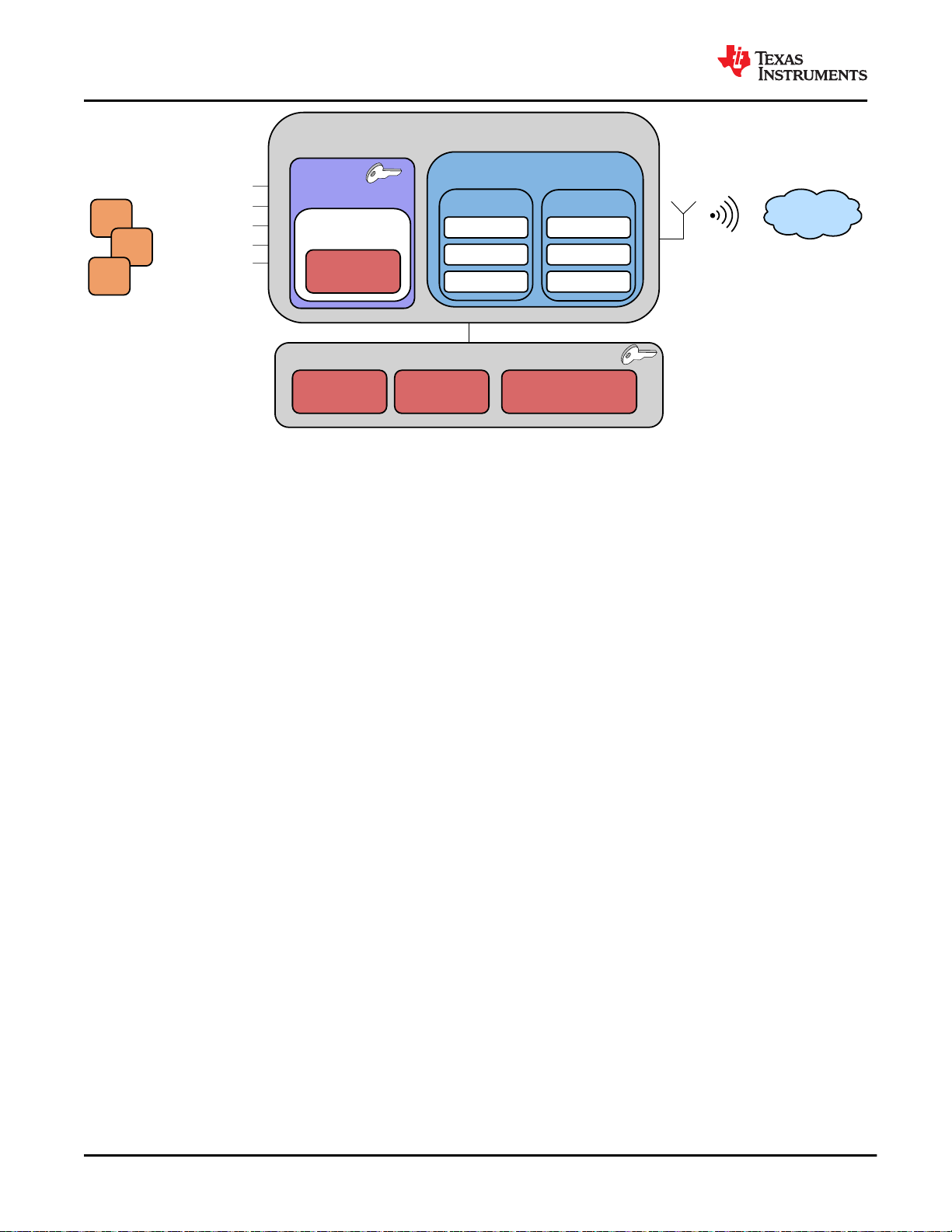
CC3235S and CC3235SF
Network Processor + MCU
Network Processor
Wi-Fi® Internet
Peripherals
OEM
Application
Serial Flash
Data Files
OEM
Application
Network Information
Dual-Band Radio
Baseband
MACHTTPS
TLS/SSL
TCP/IP
MCU
ARM® Cortex®-M4
Processor
256KB RAM /
1MB Flash (CC3235SF)
SPI and I2C
GPIO
UART
PWM
ADC
-
Internet
CC3235MODS, CC3235MODSF, CC3235MODAS, CC3235MODASF
SWRS243A – FEBRUARY 2020 – REVISED MAY 2020
www.ti.com
Figure 9-2. CC3235S and CC3235SF High-Level Structure
9.6 FIPS 140-2 Level 1 Certification
The Federal Information Processing Standard (FIPS) Publication 140-2 is a U.S. government computer security
standard. It is commonly referred to as FIPS 140-2, and is used to accredit the design and implementation of
cryptographic functions, for example within a chip. A cryptographic function within a chip security system is
necessary to maintain the confidentiality and integrity of the information that is being processed.
The security functions of the CC3235x chip that is inside the CC3235MODx or CC3235MODAx module, are
FIPS certified to FIPS 140-2 level 1. This certification covers topics such as: cryptographic specifications, ports
and interfaces, a finite state model for the cryptographic functions, the operational environment of the function,
and how cryptographic keys are managed. The certification provides the assurance that the implementation
meets FIPS 140-2 level 1 standards.
9.7 Power-Management Subsystem
The CC3235MODx and CC3235MODAx power-management subsystems contain DC/DC converters to
accommodate the differing voltage or current requirements of the system.
The CC3235MODx and CC3235MODAx MCU is a fully integrated module-based WLAN radio solution used on
an embedded system with a wide-voltage supply range. The internal power management, including DC/DC
converters and LDOs, generates all of the voltages required for the module to operate from a wide variety of
input sources. For maximum flexibility, the module can operate in the modes described in the following sections.
9.7.1 VBAT Wide-Voltage Connection
In the wide-voltage battery connection, the module can be directly connected to two AA alkaline batteries. All
other voltages required to operate the module are generated internally by the DC/DC converters. This scheme is
the most common mode for the module because it supports wide-voltage operation from 2.3 to 3.6 V.
9.8 Low-Power Operating Mode
From a power-management perspective, the CC3235MODx and CC3235MODAx MCU comprises the following
two independent subsystems:
• Arm Cortex-M4 application processor subsystem
• Networking subsystem
Each subsystem operates in one of several power states.
70 Submit Document Feedback
Product Folder Links: CC3235MODS CC3235MODSF CC3235MODAS CC3235MODASF
Copyright © 2020 Texas Instruments Incorporated
www.ti.com
SWRS243A – FEBRUARY 2020 – REVISED MAY 2020
The Arm Cortex-M4 application processor runs the user application loaded from an internal serial flash, or onmodule XIP flash (in CC3235MODSF). The networking subsystem runs preprogrammed TCP/IP and Wi-Fi data
link layer functions.
The user program controls the power state of the application processor subsystem and can be in one of the five
modes described in Table 9-2.
Table 9-2. User Program Modes
CC3235MODS, CC3235MODSF, CC3235MODAS, CC3235MODASF
APPLICATION PROCESSOR
(MCU) MODE
MCU active mode MCU executing code at 80-MHz state rate.
MCU sleep mode
MCU LPDS mode
MCU hibernate mode
MCU shutdown mode
(1)
The MCU clocks are gated off in sleep mode and the entire state of the device is retained. Sleep mode
offers instant wakeup. The MCU can be configured to wake up by an internal fast timer or by activity
from any GPIO line or peripheral.
State information is lost and only certain MCU-specific register configurations are retained. The MCU
can wake up from external events or by using an internal timer. (The wake-up time is less than 3 ms.)
Certain parts of memory can be retained while the MCU is in LPDS mode. The amount of memory
retained is configurable. Users can choose to preserve code and the MCU-specific setting. The MCU
can be configured to wake up using the RTC timer or by an external event on specific GPIOs as the
wake-up source.
The lowest power mode in which all digital logic is power-gated. Only a small section of the logic directly
powered by the input supply is retained. The RTC keeps running and the MCU supports wakeup from an
external event or from an RTC timer expiry. Wake-up time is longer than LPDS mode at about 15 ms
plus the time to load the application from serial flash, which varies according to code size. In this mode,
the MCU can be configured to wake up using the RTC timer or external event on a GPIO.
The lowest power mode system-wise. All device logics are off, including the RTC. The wake-up time in
this mode is longer than hibernate at about 1.1 s. To enter or exit the shutdown mode, the state of the
nRESET line is changed (low to shut down, high to turn on).
DESCRIPTION
(1) Modes are listed in order of power consumption, with highest power modes listed first.
The NWP can be active or in LPDS mode and takes care of its own mode transitions. When there is no network
activity, the NWP sleeps most of the time and wakes up only for beacon reception (see
Table 9-3).
Table 9-3. Networking Subsystem Modes
NETWORK PROCESSOR
Network active mode
(processing layer 3, 2, and 1)
Network active mode
(processing layer 2 and 1)
Network active listen mode Special power optimized active mode for receiving beacon frames (no other frames supported)
Network connected Idle
Network LPDS mode
Network disabled The network is disabled
MODE
Transmitting or receiving IP protocol packets
Transmitting or receiving MAC management frames; IP processing not required.
A composite mode that implements 802.11 infrastructure power save operation. The CC3235MODx and
CC3235MODAx NWPs automatically go into LPDS mode between beacons and then wakes to active
listen mode to receive a beacon and determine if there is pending traffic at the AP. If not, the NWP
returns to LPDS mode and the cycle repeats.
Low-power state between beacons in which the state is retained by the NWP, allowing for a rapid wake
up.
DESCRIPTION
The operation of the application and network processor ensures that the module remains in the lowest power
mode most of the time to preserve battery life.
The following examples show the use of the power modes in applications:
Copyright © 2020 Texas Instruments Incorporated
Product Folder Links: CC3235MODS CC3235MODSF CC3235MODAS CC3235MODASF
Submit Document Feedback
71

CC3235MODS, CC3235MODSF, CC3235MODAS, CC3235MODASF
SWRS243A – FEBRUARY 2020 – REVISED MAY 2020
www.ti.com
• A product that is continuously connected to the network in the 802.11 infrastructure power-save mode but
sends and receives little data spends most of the time in connected idle, which is a composite of receiving a
beacon frame and waiting for the next beacon.
• A product that is not continuously connected to the network but instead wakes up periodically (for example,
every 10 minutes) to send data, spends most of the time in hibernate mode, jumping briefly to active mode to
transmit data.
72 Submit Document Feedback
Product Folder Links: CC3235MODS CC3235MODSF CC3235MODAS CC3235MODASF
Copyright © 2020 Texas Instruments Incorporated

www.ti.com
CC3235MODS, CC3235MODSF, CC3235MODAS, CC3235MODASF
SWRS243A – FEBRUARY 2020 – REVISED MAY 2020
9.9 Memory
9.9.1 Internal Memory
The CC3235x device within the CC3235MODx and CC3235MODAx modules includes on-chip SRAM to which
application programs are downloaded and executed. The application developer must share the SRAM for code
and data. The micro direct memory access (µDMA) controller can transfer data to and from SRAM and various
peripherals. The CC3235x device ROM holds the rich set of peripheral drivers, which saves SRAM space. For
more information on drivers, see the CC3235x API list.
9.9.1.1 SRAM
The CC3235MODx and CC3235MODAx MCU family provides 256KB of on-chip SRAM. Internal RAM is capable
of selective retention during LPDS mode. This internal SRAM is at offset 0x2000 0000 of the device memory
map.
Use the µDMA controller to transfer data to and from the SRAM.
When the device enters low-power mode, the application developer can choose to retain a section of memory
based on need. Retaining the memory during low-power mode provides a faster wakeup. The application
developer can choose the amount of memory to retain in multiples of 64KB. For more information, see the API
guide.
9.9.1.2 ROM
The internal zero-wait-state ROM of the CC3235MODx and CC3235MODAx module is at address 0x0000 0000
of the device memory and is programmed with the following components:
• Bootloader
• Peripheral driver library (DriverLib) release for product-specific peripherals and interfaces
The bootloader is used as an initial program loader (when the serial flash memory is empty). The DriverLib
software library of the CC3235MODx and CC3235MODAx MCU controls on-chip peripherals with a bootloader
capability. The library performs peripheral initialization and control functions, with a choice of polled or interruptdriven peripheral support. The DriverLib APIs in ROM can be called by applications to reduce flash memory
requirements and free the flash memory to be used for other purposes.
9.9.1.3 Flash Memory
The CC3235SF device within the CC3235MODSF and CC3235MODASF modules comes with an on-chip flash
memory of 1MB that allows application code to execute in place while freeing SRAM exclusively for read-write
data. The flash memory is used for code and constant data sections and is directly attached to the ICODE/
DCODE bus of the Arm Cortex-M4 core. A 128-bit-wide instruction prefetch buffer allows maintenance of
maximum performance for linear code or loops that fit inside the buffer.
The flash memory is organized as 2-KB sectors that can be independently erased. Reads and writes can be
performed at word (32-bit) level.
9.9.1.4 Memory Map
Table 9-4 describes the various MCU peripherals and how they are mapped to the processor memory. For more
information on peripherals, see the API document.
Copyright © 2020 Texas Instruments Incorporated
Product Folder Links: CC3235MODS CC3235MODSF CC3235MODAS CC3235MODASF
Submit Document Feedback
73

CC3235MODS, CC3235MODSF, CC3235MODAS, CC3235MODASF
SWRS243A – FEBRUARY 2020 – REVISED MAY 2020
Table 9-4. Memory Map
START ADDRESS END ADDRESS DESCRIPTION COMMENT
0x0000 0000 0x0007 FFFF On-chip ROM (bootloader + DriverLib)
0x0100 0000 0x010F FFFF On-chip flash (for user application code) SF devices only
0x2000 0000 0x2003 FFFF Bit-banded on-chip SRAM
0x2200 0000 0x23FF FFFF Bit-band alias of 0x2000 0000 to 0x200F FFFF
0x4000 0000 0x4000 0FFF Watchdog timer A0
0x4000 4000 0x4000 4FFF GPIO port A0
0x4000 5000 0x4000 5FFF GPIO port A1
0x4000 6000 0x4000 6FFF GPIO port A2
0x4000 7000 0x4000 7FFF GPIO port A3
0x4000 C000 0x4000 CFFF UART A0
0x4000 D000 0x4000 DFFF UART A1
0x4002 0000 0x4000 07FF I2C A0 (master)
0x4002 4000 0x4002 4FFF GPIO group 4
0x4002 0800 0x4002 0FFF I2C A0 (slave)
0x4003 0000 0x4003 0FFF General-purpose timer A0
0x4003 1000 0x4003 1FFF General-purpose timer A1
0x4003 2000 0x4003 2FFF General-purpose timer A2
0x4003 3000 0x4003 3FFF General-purpose timer A3
0x400F7000 0x400F 7FFF Configuration registers
0x400F E000 0x400F EFFF System control
0x400F F000 0x400F FFFF µDMA
0x4200 0000 0x43FF FFFF Bit band alias of 0x4000 0000 to 0x400F FFFF
0x4401 0000 0x4401 0FFF SDIO master
0x4401 8000 0x4401 8FFF Camera Interface
0x4401 C000 0x4401 DFFF McASP
0x4402 0000 0x4402 0FFF SSPI Used for external serial flash
0x4402 1000 0x4402 1FFF GSPI Used by application processor
0x4402 5000 0x4402 5FFF MCU reset clock manager
0x4402 6000 0x4402 6FFF MCU configuration space
0x4402 D000 0x4402 DFFF Global power, reset, and clock manager (GPRCM)
0x4402 E000 0x4402 EFFF MCU shared configuration
0x4402 F000 0x4402 FFFF Hibernate configuration
0x4403 0000 0x4403 FFFF
0x4403 0000 0x4403 0FFF DTHE registers and TCP checksum
0x4403 5000 0x4403 5FFF MD5/SHA
0x4403 7000 0x4403 7FFF AES
0x4403 9000 0x4403 9FFF DES
0xE000 0000 0xE000 0FFF Instrumentation trace Macrocell
0xE000 1000 0xE000 1FFF Data watchpoint and trace (DWT)
0xE000 2000 0xE000 2FFF Flash patch and breakpoint (FPB)
0xE000 E000 0xE000 EFFF NVIC
0xE004 0000 0xE004 0FFF Trace port interface unit (TPIU)
0xE004 1000 0xE004 1FFF Reserved for embedded trace macrocell (ETM)
0xE004 2000 0xE00F FFFF Reserved
Crypto range (includes apertures for all crypto-related
blocks as follows)
™
www.ti.com
74 Submit Document Feedback
Product Folder Links: CC3235MODS CC3235MODSF CC3235MODAS CC3235MODASF
Copyright © 2020 Texas Instruments Incorporated

www.ti.com
SWRS243A – FEBRUARY 2020 – REVISED MAY 2020
9.10 Restoring Factory Default Configuration
CC3235MODS, CC3235MODSF, CC3235MODAS, CC3235MODASF
The module has an internal recovery mechanism that rolls back the file system to its predefined factory image or
restoring the factory default parameters of the device. The factory image is kept in a separate sector on the
sFLASH in a secure manner and cannot be accessed from the host processor. The following restore modes are
supported:
• None—no factory restore settings
• Enable restore of factory default parameters
• Enable restore of factory image and factory default parameters
The restore process is performed by calling software APIs, or by pulling or forcing SOP[2:0] = 011 pins and
toggling the nRESET pin from low to high.
The process is fail-safe and resumes operation if a power failure occurs before the restore is finished. The
restore process typically takes about 8 seconds, depending on the attributes of the serial flash vendor.
9.11 Boot Modes
9.11.1 Boot Mode List
The CC3235MODx and CC3235MODAx MCU implements a sense-on-power (SoP) scheme to determine the
device operation mode.
SoP values are sensed from the module pin during power up. This encoding determines the boot flow. Before
the device is taken out of reset, the SoP values are copied to a register and used to determine the device
operation mode while powering up. These values determine the boot flow as well as the default mapping for
some of the pins (JTAG, SWD, UART0). Table 9-5 lists the pull configurations.
All CC3235MODx and CC3235MODAx MCUs contain internal pulldown resistors on the SOP[2:0] lines. The
application can use SOP2 for other functions after chip has powered up. However, to avoid spurious SOP values
from being sensed at power up, TI strongly recommends using the SOP2 pin only for output signals. The SOP0
and SOP1 pins are multiplexed with the WLAN analog test pins and are not available for other functions.
Table 9-5. CC3235MODx and CC3235MODAx Functional Configurations
NAME SOP[2] SOP[1] SOP[0] SoP MODE COMMENT
Factory, lab flash, and SRAM loads
through the UART. The device waits
UARTLOAD Pullup Pulldown Pulldown LDfrUART
FUNCTIONAL_2WJ
FUNCTIONAL_4WJ Pulldown Pulldown Pulldown Fn4WJ
UARTLOAD_FUNCTIONAL_4WJ Pulldown Pullup Pulldown LDfrUART_FnWJ
Pulldown Pulldown Pullup Fn2WJ
indefinitely for the UART to load code.
The SOP bits then must be toggled to
configure the device in functional mode.
Also puts JTAG in 4-wire mode.
Functional development mode. In this
mode, 2-pin SWD is available to the
developer. TMS and TCK are available for
debugger connection.
Functional development mode. In this
mode, 4-pin JTAG is available to the
developer. TDI, TMS, TCK, and TDO are
available for debugger connection. The
default configuration for CC3235MODx
and CC3235MODAx MCUs.
Supports flash and SRAM load through
UART and functional mode. The MCU
bootloader tries to detect a UART break
on UART receive line. If the break signal
is present, the device enters the
UARTLOAD mode, otherwise, the device
enters the functional mode. TDI, TMS,
TCK, and TDO are available for debugger
connection.
Copyright © 2020 Texas Instruments Incorporated
Product Folder Links: CC3235MODS CC3235MODSF CC3235MODAS CC3235MODASF
Submit Document Feedback
75

CC3235MODS, CC3235MODSF, CC3235MODAS, CC3235MODASF
SWRS243A – FEBRUARY 2020 – REVISED MAY 2020
www.ti.com
Table 9-5. CC3235MODx and CC3235MODAx Functional Configurations (continued)
NAME SOP[2] SOP[1] SOP[0] SoP MODE COMMENT
RET_FACTORY_IMAGE Pulldown Pullup Pullup RetFactDef
When module reset is toggled, the MCU
bootloader kickstarts the procedure to
restore factory default images.
9.12 Hostless Mode
The SimpleLink™ Wi-Fi® CC3235MODx or CC3235MODAx devices incorporate a scripting ability that enables
offloading of simple tasks from the host processor. Using simple and conditional scripts, repetitive tasks can be
handled internally, which allows the host processor to remain in a low-power state. In some cases where the
scripter is being used to send packets, it reduces code footprint and memory consumption. The if-this-then-that
style conditioning can include anything from GPIO toggling to transmitting packets.
The conditional scripting abilities can be divided into conditions and actions. The conditions define when to
trigger actions. Only one action can be defined per condition, but multiple instances of the same condition may
be used, so in effect multiple actions can be defined for a single condition. In total, 16 condition and action pairs
can be defined. The conditions can be simple, or complex using sub-conditions (using a combinatorial AND
condition between them). The actions are divided into two types, those that can occur during runtime and those
that can occur only during the initialization phase.
The following actions can only be performed when triggered by the pre-initialization condition:
• Set roles AP, station, P2P, and Tag modes
• Delete all stored profiles
• Set connection policy
• Hardware GPIO indication allows an I/O to be driven directly from the WLAN core hardware to indicate
internal signaling
The following actions may be activated during runtime:
• Send transceiver packet
• Send UDP packet
• Send TCP packet
• Increment counter increments one of the user counters by 1
• Set counter allows setting a specific value to a counter
• Timer control
• Set GPIO allows GPIO output from the device using the internal networking core
• Enter Hibernate state
Note
Consider the following limitations:
• Timing cannot be ensured when using the network scripter because some variable latency will
apply depending on the utilization of the networking core.
• The scripter is limited to 16 pairs of conditions and reactions.
• Both timers and counters are limited to 8 instances each. Timers are limited to a resolution of 1
second. Counters are 32 bits wide.
• Packet length is limited to the size of one packet and the number of possible packet tokens is
limited to 8.
76 Submit Document Feedback
Product Folder Links: CC3235MODS CC3235MODSF CC3235MODAS CC3235MODASF
Copyright © 2020 Texas Instruments Incorporated

www.ti.com
CC3235MODS, CC3235MODSF, CC3235MODAS, CC3235MODASF
SWRS243A – FEBRUARY 2020 – REVISED MAY 2020
9.13 Device Certification and Qualification
The CC3235MODx and CC3235MODAx MCU from TI is certified for FCC, IC/ISED, ETSI/CE, Japan MIC, and
SRRC. Moreover, the module is also Wi-Fi CERTIFIED™ with the ability to request a certificate transfer for Wi-Fi
Alliance® members. TI customers that build products based on the CC3235MODx or CC3235MODAx MCU from
TI can save in testing cost and time per product family.
Table 9-6. CC3235MODx and CC3235MODAx List of Certifications
Regulatory Body Specification ID (IF APPLICABLE)
FCC (USA) Part 15C + MPE FCC RF Exposure Z64-CC3235MOD
IC/ISED (Canada) RSS-102 (MPE) and RSS-247 (Wi-Fi) 451I-CC3235MOD
EN300328 v2.2.1 (2.4GHz Wi-Fi) —
EN301893 v2.1.1 (5GHz Wi-Fi) —
EN62311:2008 (MPE) —
ETSI/CE (Europe)
MIC (Japan) Article 49-20 of ORRE 201-190033
SRRC (China) —
EN301489-1 v2.2.1 (General EMC) —
EN301489-17 v3.2.0 (EMC) —
EN60950-1:2006/A11:2009/A1:2010/
A12:2011/A2:2013
—
Please contact TI for more information on
using SRRC ID Certification: www.ti.com/tool/
SIMPLELINK-CC3XXX-CERTIFICATION
9.13.1 FCC Certification and Statement
CAUTION
FCC RF Radiation Exposure Statement:
This equipment complies with FCC radiation exposure limits set forth for an uncontrolled
environment. End users must follow the specific operating instructions for satisfying RF exposure
limits. This transmitter must not be co-located or operating with any other antenna or transmitter.
The CC3235MODx and CC3235MODAx modules from TI are certified for the FCC as a single-modular
transmitter. The modules are FCC-certified radio modules that carries a modular grant.
You are cautioned that changes or modifications not expressly approved by the party responsible for compliance
could void the user’s authority to operate the equipment.
This device complies with Part 15 of the FCC Rules. Operation is subject to the following two conditions:
• This device may not cause harmful interference.
• This device must accept any interference received, including interference that may cause undesired
operation of the device.
9.13.2 IC/ISED Certification and Statement
CAUTION
IC RF Radiation Exposure Statement:
To comply with IC RF exposure requirements, this device and its antenna must not be co-located or
operating in conjunction with any other antenna or transmitter.
Pour se conformer aux exigences de conformité RF canadienne l'exposition, cet appareil et son
antenne ne doivent pas étre co-localisés ou fonctionnant en conjonction avec une autre antenne ou
transmetteur.
Copyright © 2020 Texas Instruments Incorporated
Product Folder Links: CC3235MODS CC3235MODSF CC3235MODAS CC3235MODASF
Submit Document Feedback
77

CC3235MODS, CC3235MODSF, CC3235MODAS, CC3235MODASF
SWRS243A – FEBRUARY 2020 – REVISED MAY 2020
www.ti.com
The CC3235MODx and CC3235MODAx modules from TI are certified for IC as a single-modular transmitter. The
CC3235MODx and CC3235MODAx modules from TI meet IC modular approval and labeling requirements. The
IC follows the same testing and rules as the FCC regarding certified modules in authorized equipment.
This device complies with Industry Canada licence-exempt RSS standards.
Operation is subject to the following two conditions:
• This device may not cause interference.
• This device must accept any interference, including interference that may cause undesired operation of the
device.
Le présent appareil est conforme aux CNR d'Industrie Canada applicables aux appareils radio exempts de
licence.
L'exploitation est autorisée aux deux conditions suivantes:
• L'appareil ne doit pas produire de brouillage
• L'utilisateur de l'appareil doit accepter tout brouillage radioélectrique subi, même si le brouillage est
susceptible d'en compromettre le fonctionnement.
9.13.3 ETSI/CE Certification
The CC3235MODx and CC3235MODAx modules from TI are CE certified with certifications to the appropriate
EU radio and EMC directives summarized in the Declaration of Conformity and evidenced by the CE mark. The
modules are tested against the new Radio Equipment Directive (RE-D). See the full text of the EU Declaration of
Conformity for the CC3235MODSM2MOB and CC3235MODSF12MOB devices.
9.13.4 MIC Certification
The CC3235MODx and CC3235MODAx modules from TI are MIC certified against article 49-20 and the relevant
articles of the Ordinance Regulating Radio Equipment.
Operation is subject to the following condition:
• The host system does not contain a wireless wide area network (WWAN) device.
This device operates in the W52 and W53 bands and is for indoor use only (except communication to high power
radio).
78 Submit Document Feedback
Product Folder Links: CC3235MODS CC3235MODSF CC3235MODAS CC3235MODASF
Copyright © 2020 Texas Instruments Incorporated
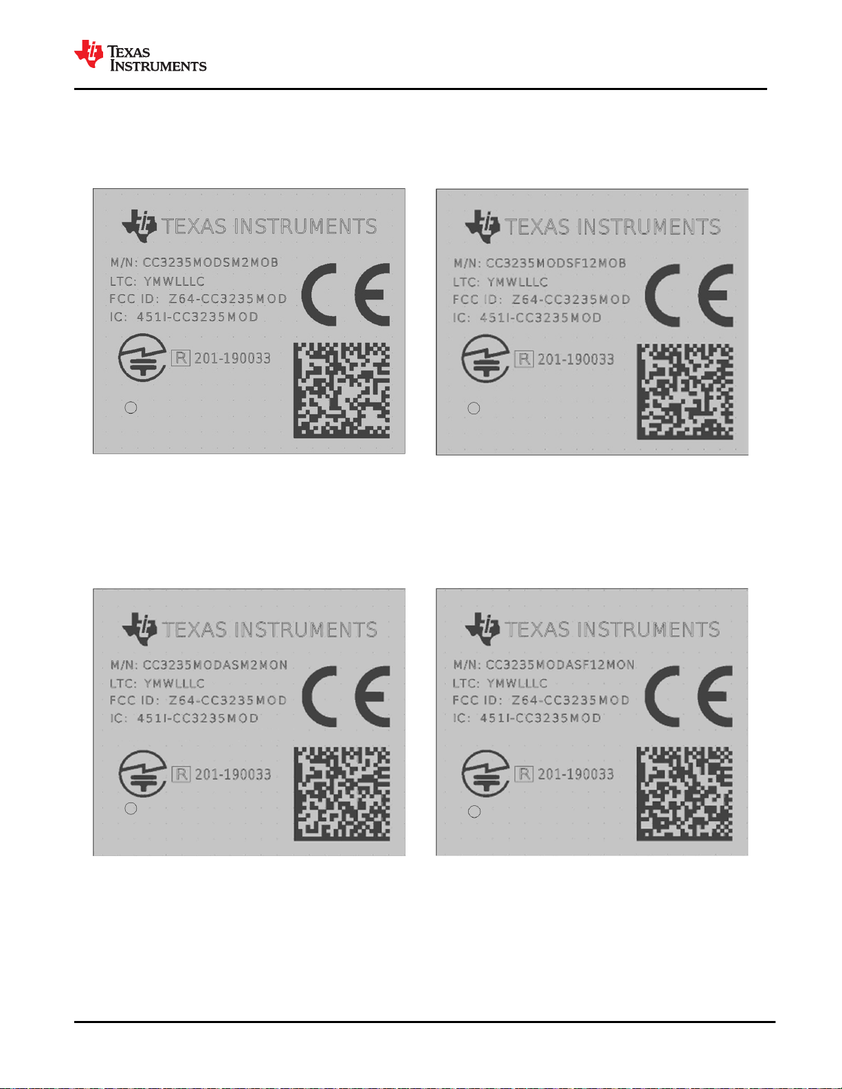
www.ti.com
CC3235MODS, CC3235MODSF, CC3235MODAS, CC3235MODASF
SWRS243A – FEBRUARY 2020 – REVISED MAY 2020
9.14 Module Markings
Figure 9-3 and Figure 9-4 show the markings for the SimpleLink™ CC3235MODx module.
Figure 9-3. CC3235MODS Module Marking
Figure 9-4. CC3235MODSF Module Marking
Figure 9-5 and Figure 9-6 show the markings for the SimpleLink™ CC3235MODAx modules.
Figure 9-5. CC3235MODAS Module Marking
Copyright © 2020 Texas Instruments Incorporated
Product Folder Links: CC3235MODS CC3235MODSF CC3235MODAS CC3235MODASF
Figure 9-6. CC3235MODASF Module Marking
Submit Document Feedback
79

R 201-190033
CC3235MODS, CC3235MODSF, CC3235MODAS, CC3235MODASF
SWRS243A – FEBRUARY 2020 – REVISED MAY 2020
Table 9-7 lists the CC3235MODx and CC3235MODAx module markings.
Table 9-7. Module Descriptions
MARKING DESCRIPTION
CC3235MODSM2MOB
CC3235MODSF12MOB
CC3235MODASM2MON
CC3235MODASF12MON
YMWLLLC
Z64-CC3235MOD FCC ID: single modular FCC grant ID
451I-CC3235MOD IC: single modular IC grant ID
CE CE compliance mark
Model
Model
LTC (Lot Trace Code):
• Y = Year
• M = Month
• WLLLC = Reserved for internal use
MIC compliance mark
MIC ID: modular MIC grant ID
www.ti.com
9.15 End Product Labeling
These modules are designed to comply with the FCC single modular FCC grant, FCC ID: Z64-CC3235MOD.
The host system using this module must display a visible label indicating the following text:
Contains FCC ID: Z64-CC3235MOD
These modules are designed to comply with the IC single modular FCC grant, IC: 451I-CC3235MOD. The host
system using this module must display a visible label indicating the following text:
Contains IC: 451I-CC3235MOD
This module is designed to comply with the JP statement, 201-190033. The host system using this module must
display a visible label indicating the following text:
Contains transmitter module with certificate number: 201-190033
9.16 Manual Information to the End User
The OEM integrator must be aware not to provide information to the end user regarding how to install or remove
this RF module in the user’s manual of the end product which integrates this module.
The end user manual must include all required regulatory information and warnings as shown in this manual.
80 Submit Document Feedback
Product Folder Links: CC3235MODS CC3235MODSF CC3235MODAS CC3235MODASF
Copyright © 2020 Texas Instruments Incorporated
WLAN
CC3235MODx
BLE
CCxxxx
RF_ABG
RF
Coex IO
CC_COEX_BLE_IN
Dual-band Antenna BLE Ant.
www.ti.com
CC3235MODS, CC3235MODSF, CC3235MODAS, CC3235MODASF
SWRS243A – FEBRUARY 2020 – REVISED MAY 2020
10 Applications, Implementation, and Layout
Note
Information in the following applications sections is not part of the TI component specification, and TI
does not warrant its accuracy or completeness. TI’s customers are responsible for determining
suitability of components for their purposes. Customers should validate and test their design
implementation to confirm system functionality.
10.1 Typical Application
10.1.1 BLE/2.4 GHz Radio Coexistence
The CC3235MODx and CC3235MODAx devices are designed to support BLE/2.4 GHz radio coexistence.
Because WLAN is inherently more tolerant to time-domain disturbances, the coexistence mechanism gives
priority to the Bluetooth® low energy entity over the WLAN. Bluetooth® low energy operates in the 2.4 GHz band,
therefore the coexistence mechanism does not affect the 5 GHz band. The CC3235MODx and CC3235MODAx
device can operate normally on the 5 GHz band, while the Bluetooth® low energy works on the 2.4 GHz band
without mutual interference.
The following coexistence modes can be configured by the user:
• Off mode or intrinsic mode
– No BLE/2.4 GHz radio coexistence, or no synchronization between WLAN and Bluetooth® low energy—in
case Bluetooth® low energy exists in this mode, collisions can randomly occur.
• Time Division Multiplexing (TDM, Dual Antenna)
– Dual-band Wi-Fi (see Figure 10-1)
In this mode, the WLAN can operate on either a 2.4 or 5 GHz band and Bluetooth® low energy operates
on the 2.4 GHz band.
Figure 10-1 shows the dual antenna implementation of a complete Bluetooth® low energy and WLAN
coexistence network with the WLAN operating on either a 2.4- or a 5 GHz band. Note in this implementation a
Coex switch is not required and only a single GPIO from the BLE device to the CC3235MOD device is needed.
In addition, the CC3235MODx's antenna is external while the CC3235MODAx's antenna is integrated.
Figure 10-1. Dual-Antenna Coexistence Mode Block Diagram
Copyright © 2020 Texas Instruments Incorporated
Submit Document Feedback
Product Folder Links: CC3235MODS CC3235MODSF CC3235MODAS CC3235MODASF
81

BLE
CCxxxx
WLAN
CC3235MODx
RF
CC_COEX_BLE_IN
RF_ABG
Coex IO
Antenna Selection
SPDT RF Switch
ANT_SEL_1
ANT_SEL_2
Dual Band Ant. 1
Dual Band Ant. 2
BLE Ant.
CC3235MODS, CC3235MODSF, CC3235MODAS, CC3235MODASF
SWRS243A – FEBRUARY 2020 – REVISED MAY 2020
www.ti.com
10.1.2 Antenna Selection (CC3235MODx only)
The CC3235MODx device is designed to also support antenna selection and is controlled from Image Creator.
When enabled, there are 3 options possible options:
• ANT 1: When selected, the GPIOs that are defined for antenna selection with set the RF path for antenna 1.
• ANT 2: When selected, the GPIOs that are defined for antenna selection will set the RF path for antenna 2.
• Autoselect: When selected, during a scan and prior to connecting to an AP, CC3235MODx device will
determine the best RF path and select the appropriate antenna 13 14. The result is the saved as port of the
profile.
Figure 10-2 shows the antenna selection implementation for Wi-Fi, with BLE operating on it's own antenna. Note
in this implementation, only a single GPIO from the BLE device to the CC3235MODx device is required. The
Antenna switch 15is controlled by 2 GPIO lines from the CC3235MODx device. Section 7.3 lists which GPIOs
can be used for Antenna Selection.
Figure 10-2. Coexistence Solution with Wi-Fi Antenna Selection and Dedicated BLE Antenna
13
When selecting Autoselect via the API, a reset is required in order for the CC3235MODx device to
determine the best antenna for use.
14
Refer to the Uniflash with Image Creator User Guidefor more information.
15
The recommended Antenna switch is the Richwave RTC6608OSP.
82 Submit Document Feedback
Copyright © 2020 Texas Instruments Incorporated
Product Folder Links: CC3235MODS CC3235MODSF CC3235MODAS CC3235MODASF

www.ti.com
CC3235MODS, CC3235MODSF, CC3235MODAS, CC3235MODASF
SWRS243A – FEBRUARY 2020 – REVISED MAY 2020
10.1.3 Typical Application Schematic (CC3235MODx)
Figure 10-3 shows the typical application schematic using the CC3235MODx module. See the full reference schematic for CC3235MODx.
Note that the CC3235MODx and CC3235MODAx modules share the same reference schematic. The difference between the two references is the
antenna and its matching circuitry. The CC3235MODAx's pin 31 is not accessible to the designer because it is directly tied to the integrated antenna.
Note
The following guidelines are recommended for implementation of the RF design:
• Ensure an RF path is designed with an impedance of 50 Ω
• Tuning of the antenna impedance π matching network is recommended after manufacturing of the PCB to account for PCB parasitics
• π or L matching and tuning may be required between cascaded passive components on the RF path
Copyright © 2020 Texas Instruments Incorporated
Product Folder Links: CC3235MODS CC3235MODSF CC3235MODAS CC3235MODASF
Submit Document Feedback
83
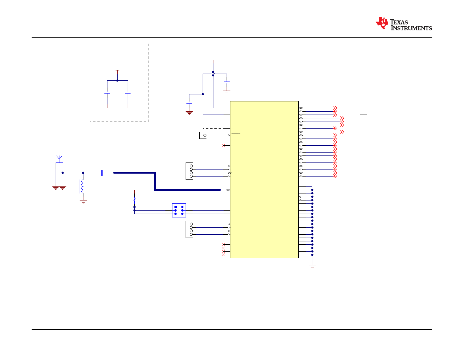
P50_GPIO_00
P55_GPIO_01
P57_GPIO_02
P58_GPIO_03
P59_GPIO_04
P60_GPIO_05
P61_GPIO_06
P62_GPIO_07
P63_GPIO_08
P64_GPIO_09
P01_GPIO_10
P02_GPIO_11
P03_GPIO_12
P04_GPIO_13
P07_GPIO_16
P08_GPIO_17
P15_GPIO_22
P18_GPIO_28
P53_GPIO_30
P05_GPIO_14
P06_GPIO_15
VBAT_CC
GND
GND
1
GND
2
GPIO10
3
GPIO11
4
GPIO14
5
GPIO15
6
GPIO16
7
GPIO17
8
GPIO12
9
GPIO13
10
GPIO22
11
JTAG_ TDI
12
FLASH_SPI_MISO
13
FLASH_SPI_CS_IN
14
FLASH_SPI_CLK
15
GND
16
FLASH_SPI_MOSI
17
JTAG_ TDO
18
GPIO28
19
NC
20
JTAG_ TCK
21
JTAG_ TMS
22
SOP2
23
SOP1
24
GND
25
GND
26
GND
27
GND
28
GND
29
GND
30
RF_ABG
31
GND
32
NC
33
SOP0
34
RESET
35
VBAT_RESET
36
VBAT1
37
GND
38
NC
39
VBAT2
40
NC
41
GPIO30
42
GND
43
GPIO0
44
NC
45
GPIO01
46
GPIO02
47
GPIO03
48
GPIO04
49
GPIO05
50
GPIO06
51
GPIO07
52
GPIO08
53
GPIO09
54
GND
55
GND
56
GND
57
GND
58
GND
59
GND
60
GND
61
GND
62
GND
63
CC3235MODSF12MOBR
CC1
JTAG/DEBUG
EXTERNAL
PROGRAMMING
1 2
3 4
5 6
J1
10k
R1
VBAT_CC
RF_ABG
GNDGND
4.7nH
L1
0.1uF
C2
0.1uF
C1
GND
GND
SEE TABLE 4-1 FOR
VBAT_RESET and nRESET
CONNECTION OPTIONS
At a minimum, pull thesepin s out
to test pointsto aid in debug:
Pin 48: RS232_TX
Pin 49: RS232_RX
Pin 50: WLAN_LOG
Pin 52: NWP_LOG
SOP[2:0] USED TO CONFIGUREBOOT MODES (TABLE 5-5)
GND
1
2
E1
Matching circuit shown below is for
the antenna. The moduleis matched
internallyto 50 ©. Final solution
mayrequire antennamatching
optimization with a pi-network.
100uF
C4
100uF
C5
GND G ND
VBAT_CC
Optional:
Consider adding extra decoupling
capaci tors ifthe battery cannot source
the peak cu rrents.
1pF
C3
CC3235MODS, CC3235MODSF, CC3235MODAS, CC3235MODASF
SWRS243A – FEBRUARY 2020 – REVISED MAY 2020
84 Submit Document Feedback
Figure 10-3. CC3235MODx Typical Application Schematic
Product Folder Links: CC3235MODS CC3235MODSF CC3235MODAS CC3235MODASF
www.ti.com
Copyright © 2020 Texas Instruments Incorporated

www.ti.com
SWRS243A – FEBRUARY 2020 – REVISED MAY 2020
Table 10-1 provides the bill of materials for a typical application using the CC3235MODx module in Figure 10-3.
For full operation reference design, see the CC3235MODAx SimpleLink™ and Internet of Things Hardware Design Files.
Table 10-1. Bill of Materials
CC3235MODS, CC3235MODSF, CC3235MODAS, CC3235MODASF
QTY PART REFERENCE VALUE MANUFACTURER PART NUMBER DESCRIPTION
2 C1, C2 0.1 µF Murata GRM155R61A104KA01D Capacitor, ceramic, 0.1 µF, 10 V, ±10%, X5R, 0402
1 C3 1 pF Murata GRM1555C1H1R0CA01D Capacitor, ceramic, 1 pF, 50 V, ±5%, C0G/NP0, 0402
2 C4, C5 100 µF Murata LMK325ABJ107MMHT Capacitor, ceramic, 100 µF, 10 V, ±20%, X5R, AEC-
1 E1 2.4 GHz, 5 GHz Ant Ethertronics M830520 Antenna Bluetooth WLAN Zigbee
1 L1 4.7 nH Murata LQG15HS4N7C02D Inductor, Multilayer, Air Core, 4.7nH, 0.7 A, 0.16 Ω,
1 R1 10k Vishay-Dale CRCW040210K0JNED RES, 10k, 5%, 0.063 W, AEC-Q200 Grade 0, 0402
1 CC1 CC3235MODx Texas Instruments CC3235MODSM2MOB/
CC3235MODSF12MOB
Q200 Grade 3, 1210
®
SMD
SimpleLink™ Wi-Fi® and Internet-of-Things Module
Solution, a Single-Chip Wireless Dual-Band MCU,
MOB0063A
Copyright © 2020 Texas Instruments Incorporated
Product Folder Links: CC3235MODS CC3235MODSF CC3235MODAS CC3235MODASF
Submit Document Feedback
85

P50_GPIO_00
P55_GPIO_01
P57_GPIO_02
P58_GPIO_03
P59_GPIO_04
P60_GPIO_05
P61_GPIO_06
P62_GPIO_07
P63_GPIO_08
P64_GPIO_09
P01_GPIO_10
P02_GPIO_11
P03_GPIO_12
P04_GPIO_13
P07_GPIO_16
P08_GPIO_17
P15_GPIO_22
P18_GPIO_28
P53_GPIO_30
P05_GPIO_14
P06_GPIO_15
VBAT_CC
GND
JTAG/DEBUG
EXTERNAL
1 2
PROGRAMMING
3
4
5 6
J1
10k
R1
VBAT_CC
C2
0.1uF
0.1uF
C1
GND
GND
SEE TABLE 4-1 FOR
VBAT_RESET and nRESET
CONNECTION OPTIONS
At a minimum, pull these pins out
to test points to aid in debug:
Pin 48: RS232_TX
Pin 49: RS232_RX
Pin 50: WLAN_LOG
Pin 52: NWP_LOG
C4
100uF
C5
100uF
SOP[2:0] USED TO CONFIGURE BOOT MODES (TABLE 5-5)
GND GND
VBAT_CC
1
GND
2
GND
3
GPIO_10
4
GPIO_11
5
GPIO_14
Optional:
Consider adding extra decoupling
capacitors if the battery cannot source
the peak currents.
6
GPIO_15
7
GPIO_16
8
GPIO_17
9
GPIO_12
10
GPIO_13
11
GPIO_22
12
JTAG_TDI
13
FLASH_SPI_MISO
14
FLASH_SPI_CS_IN
15
GND
16
FLASH_SPI_CLK
17
FLASH_SPI_MOSI
18
JTAG_TDO
19
GPIO_28
NC
20
21
JTAG_TCK
22
JTAG_TMS
23
SOP2
SOP1
24
GND
27
GND
28
GND
29
GND
30
31
RF_ABG
GND
32
NC
33
SOP0
34
35
RESET
36
VBAT_RESET
VBAT1
37
GND
38
NC
39
40
VBAT2
NC
41
42
GPIO_30
GND
43
44
GPIO_0
NC
45
46
GPIO_01
47
GPIO_02
48
GPIO_03
49
GPIO_04
50
GPIO_05
51
GPIO_06
52
GPIO_07
53
GPIO_08
54
GPIO_09
GND
55
GND
56
GND
57
GND
58
GND
59
GND
60
GND
61
GND
62
GND
63
GND
25
GND
26
CC?
GND
CC3235MODASM2MONR
GND
CC3235MODS, CC3235MODSF, CC3235MODAS, CC3235MODASF
SWRS243A – FEBRUARY 2020 – REVISED MAY 2020
10.1.4 Typical Application Schematic (CC3235MODAx)
Figure 10-4 shows the typical application schematic using the CC3235MODAx module. See the full reference schematic for CC3235MODAx.
86 Submit Document Feedback
Figure 10-4. CC3235MODAx Typical Application Schematic
Product Folder Links: CC3235MODS CC3235MODSF CC3235MODAS CC3235MODASF
Copyright © 2020 Texas Instruments Incorporated
www.ti.com

www.ti.com
SWRS243A – FEBRUARY 2020 – REVISED MAY 2020
Table 10-2 provides the bill of materials for a typical application using the CC3235MODAx module in Figure 10-4.
For full operation reference design, see the CC3235MODAx SimpleLink™ and Internet of Things Hardware Design Files.
Table 10-2. Bill of Materials
CC3235MODS, CC3235MODSF, CC3235MODAS, CC3235MODASF
QTY PART REFERENCE VALUE MANUFACTURER PART NUMBER DESCRIPTION
2 C1, C2 0.1 µF Murata GRM155R61A104KA01D Capacitor, ceramic, 0.1 µF, 10 V, ±10%, X5R, 0402
2 C4, C5 100 µF Murata LMK325ABJ107MMHT Capacitor, ceramic, 100 µF, 10 V, ±20%, X5R, AEC-
1 R1 10k Vishay-Dale CRCW040210K0JNED RES, 10k, 5%, 0.063 W, AEC-Q200 Grade 0, 0402
1 CC1 CC3235MODAx Texas Instruments CC3235MODASM2MON/
CC3235MODASF12MON
Q200 Grade 3, 1210
SimpleLink™ Wi-Fi® and Internet-of-Things Module
Solution, a Single-Chip Wireless Dual-Band MCU,
MON0063A
Copyright © 2020 Texas Instruments Incorporated
Product Folder Links: CC3235MODS CC3235MODSF CC3235MODAS CC3235MODASF
Submit Document Feedback
87

CC3235MODS, CC3235MODSF, CC3235MODAS, CC3235MODASF
SWRS243A – FEBRUARY 2020 – REVISED MAY 2020
www.ti.com
10.2 Device Connection and Layout Fundamentals
10.2.1 Power Supply Decoupling and Bulk Capacitors
Depending upon routing resistors and battery type, TI recommends adding two 100-µF ceramic capacitors to
help provide the peak current drawn by the CC3235MODx and CC3235MODAx modules.
Note
The module enters a brown-out condition whenever the input voltage dips below V
BROWN
(see Figure
8-4 and Figure 8-5). This condition must be considered during design of the power supply routing
specifically if operating from a battery. For more details on brown-out consideration, see Section 8.8.
10.2.2 Reset
The module features an internal RC circuit to reset the device during power ON. The nRESET pin must be held
below 0.6 V for at least 5 ms for the device to successfully reset.
10.2.3 Unused Pins
All unused pins can be left unconnected without the concern of having leakage current.
10.3 PCB Layout Guidelines
This section details the PCB guidelines to speed up the PCB design using the CC3235MODx and
CC3235MODAx. The integrator of theCC3235MODx and CC3235MODAx modules must comply with the PCB
layout recommendations described in the following subsections to minimize the risk with regulatory certifications
for the FCC, IC/ISED, ETSI/CE, MIC, and SRRC. Moreover, TI recommends customers follow the guidelines
described in this section to achieve similar performance to that obtained with the TI reference design.
10.3.1 General Layout Recommendations
Ensure that the following general layout recommendations are followed:
• Have a solid ground plane and ground vias under the module for stable system and thermal dissipation.
• Do not run signal traces underneath the module on a layer where the module is mounted.
10.3.2 CC3235MODx RF Layout Recommendations
The RF section of this wireless module gets top priority in terms of layout. It is very important for the RF section
to be laid out correctly to ensure optimum performance from the module. A poor layout can cause low-output
power, EVM degradation, sensitivity degradation, and mask violations.
Figure 10-5 shows the RF placement and routing of the CC3235MODx module with external antenna.
88 Submit Document Feedback
Product Folder Links: CC3235MODS CC3235MODSF CC3235MODAS CC3235MODASF
Copyright © 2020 Texas Instruments Incorporated

www.ti.com
CC3235MODS, CC3235MODSF, CC3235MODAS, CC3235MODASF
SWRS243A – FEBRUARY 2020 – REVISED MAY 2020
Figure 10-5. RF Section Layout
Follow these RF layout recommendations for the CC3235MODx device:
• RF traces must have 50-Ω impedance.
• RF trace bends must be made with gradual curves, and 90° bends must be avoided.
• RF traces must not have sharp corners.
• There must be no traces or ground under the antenna section.
• RF traces must have via stitching on the ground plane beside the RF trace on both sides.
• RF traces must be as short as possible. The antenna, RF traces, and the module must be on the edge of the
PCB product in consideration of the product enclosure material and proximity.
Copyright © 2020 Texas Instruments Incorporated
Product Folder Links: CC3235MODS CC3235MODSF CC3235MODAS CC3235MODASF
Submit Document Feedback
89

Copyright © 2017, Texas Instruments Incorporated
CC3235MODS, CC3235MODSF, CC3235MODAS, CC3235MODASF
SWRS243A – FEBRUARY 2020 – REVISED MAY 2020
www.ti.com
For optimal RF performance, ensure the copper cut out on the top layer under the RF-BG pin (pin 31) is as
shown in Figure 10-6.
Figure 10-6. Top Layer Copper Pullback on RF Pads
90 Submit Document Feedback
Product Folder Links: CC3235MODS CC3235MODSF CC3235MODAS CC3235MODASF
Copyright © 2020 Texas Instruments Incorporated

www.ti.com
SWRS243A – FEBRUARY 2020 – REVISED MAY 2020
10.3.2.1 Antenna Placement and Routing
The antenna is the element used to convert the guided waves on the PCB traces to the free space
electromagnetic radiation. The placement and layout of the antenna are the keys to increased range and data
rates. Table 10-3 provides a summary of the recommended antennas to use with the CC3235MODx module.
Table 10-3. Antenna Guidelines
SR NO. GUIDELINES
1 Place the antenna on an edge or corner of the PCB.
CC3235MODS, CC3235MODSF, CC3235MODAS, CC3235MODASF
2
3
4
5
6
7 Ensure that the antenna has a near omnidirectional pattern.
8
Ensure that no signals are routed across the antenna elements on all the layers of the
PCB.
Most antennas, including the chip antenna used on the LaunchPad™, require ground
clearance on all the layers of the PCB. Ensure that the ground is cleared on inner layers
as well.
Ensure that there is provision to place matching components for the antenna. These must
be tuned for best return loss when the complete board is assembled. Any plastics or
casing must also be mounted while tuning the antenna because this can impact the
impedance.
Ensure that the antenna impedance is 50 Ω because the module is rated to work only with
a 50-Ω system.
In case of printed antenna, ensure that the simulation is performed with the solder mask in
consideration.
The feed point of the antenna is required to be grounded. This is only for the antenna type
used on the CC3235MODx Launchpad. See the specific antenna data sheets for the
recommendations.
Table 10-4 lists the recommended antennas to use with the CC3235MODx module. Other antennas may be
available for use with the CC3235MODx modules.
Table 10-4. Recommended Components
CHOICE PART NUMBER MANUFACTURER NOTES
1 M830520 Ethertronics
Can be placed on edge of the PCB and uses much less PCB
space
Copyright © 2020 Texas Instruments Incorporated
Product Folder Links: CC3235MODS CC3235MODSF CC3235MODAS CC3235MODASF
Submit Document Feedback
91
S
W
CC3235MODS, CC3235MODSF, CC3235MODAS, CC3235MODASF
SWRS243A – FEBRUARY 2020 – REVISED MAY 2020
www.ti.com
10.3.2.2 Transmission Line Considerations
The RF signal from the module is routed to the antenna using a Coplanar Waveguide with ground (CPW-G)
structure. CPW-G structure offers the maximum amount of isolation and the best possible shielding to the RF
lines. In addition to the ground on the L1 layer, placing GND vias along the line also provides additional
shielding.
Figure 10-7 shows a cross section of the coplanar waveguide with the critical dimensions.
Figure 10-8 shows the top view of the coplanar waveguide with GND and via stitching.
Figure 10-7. Coplanar Waveguide (Cross Section)
Figure 10-8. CPW With GND and Via Stitching (Top View)
92 Submit Document Feedback
Product Folder Links: CC3235MODS CC3235MODSF CC3235MODAS CC3235MODASF
Copyright © 2020 Texas Instruments Incorporated

www.ti.com
SWRS243A – FEBRUARY 2020 – REVISED MAY 2020
The recommended values for the PCB are provided for 2-layer boards in Table 10-5 and 4-layer boards in Table
10-6.
Table 10-5. Recommended PCB Values for 2-Layer
Board (L1 to L2 = 42.1 mils)
CC3235MODS, CC3235MODSF, CC3235MODAS, CC3235MODASF
PARAMETER VALUE UNIT
W 26 mils
S 5.5 mils
H 42.1 mils
Er (FR-4 substrate) 4.2 F/m
Table 10-6. Recommended PCB Values for 4-Layer
Board (L1 to L2 = 16 mils)
PARAMETER VALUE UNITS
W 21 mils
S 10 mils
H 16 mils
Er (FR-4 substrate) 4.5 F/m
Copyright © 2020 Texas Instruments Incorporated
Product Folder Links: CC3235MODS CC3235MODSF CC3235MODAS CC3235MODASF
Submit Document Feedback
93

CC3235MODS, CC3235MODSF, CC3235MODAS, CC3235MODASF
SWRS243A – FEBRUARY 2020 – REVISED MAY 2020
www.ti.com
10.3.3 CC3235MODAx RF Layout Recommendations
Use the following guidelines to lay out the CC3235MODAx module with an integrated antenna, as shown in
Figure 10-9.
• The module must have an overhang of 1 mm from the PCB edge.
• The module must have a 6-mm clearance on all layers (no copper) to the left and right of the module
placement.
• There must be at least one ground-reference plane under the module on the main PCB.
Figure 10-9. CC3235MODAx Layout Guidelines
94 Submit Document Feedback
Product Folder Links: CC3235MODS CC3235MODSF CC3235MODAS CC3235MODASF
Copyright © 2020 Texas Instruments Incorporated

www.ti.com
CC3235MODS, CC3235MODSF, CC3235MODAS, CC3235MODASF
SWRS243A – FEBRUARY 2020 – REVISED MAY 2020
11 Environmental Requirements and SMT Specifications
11.1 PCB Bending
The PCB follows IPC-A-600J for PCB twist and warpage < 0.75% or 7.5 mil per inch.
11.2 Handling Environment
11.2.1 Terminals
The product is mounted with motherboard through land-grid array (LGA). To prevent poor soldering, do not make
skin contact with the LGA portion.
11.2.2 Falling
The mounted components will be damaged if the product falls or is dropped. Such damage may cause the
product to malfunction.
11.3 Storage Condition
11.3.1 Moisture Barrier Bag Before Opened
A moisture barrier bag must be stored in a temperature of less than 30°C with humidity under 85% RH. The
calculated shelf life for the dry-packed product will be 24 months from the date the bag is sealed.
11.3.2 Moisture Barrier Bag Open
Humidity indicator cards must be blue, < 30%.
11.4 PCB Assembly Guide
The wireless MCU modules are packaged in a substrate base Leadless Quad Flatpack (QFM) package.
Components were mounted onto the substrate with standard SMT process with the additional of a metal lid
covering the top of the module. The module are designed with pull back leads for easy PCB layout and board
mounting.
11.4.1 PCB Land Pattern & Thermal Vias
We recommended a solder mask defined land pattern to provide a consistent soldering pad dimension in order
to obtain better solder balancing and solder joint reliability. PCB land pattern are 1:1 to module soldering pad
dimension. Thermal vias on PCB connected to other metal plane are for thermal dissipation purpose. It is critical
to have sufficient thermal vias to avoid device thermal shutdown. Recommended vias size are 0.2mm and
position not directly under solder paste to avoid solder dripping into the vias.
11.4.2 SMT Assembly Recommendations
The module surface mount assembly operations include:
• Screen printing the solder paste on the PCB
• Monitor the solder paste volume (uniformity)
• Package placement using standard SMT placement equipment
• X-ray pre-reflow check - paste bridging
• Reflow
• X-ray post-reflow check - solder bridging and voids
Copyright © 2020 Texas Instruments Incorporated
Product Folder Links: CC3235MODS CC3235MODSF CC3235MODAS CC3235MODASF
Submit Document Feedback
95

CC3235MODS, CC3235MODSF, CC3235MODAS, CC3235MODASF
SWRS243A – FEBRUARY 2020 – REVISED MAY 2020
www.ti.com
11.4.3 PCB Surface Finish Requirements
A uniform PCB plating thickness is key for high assembly yield. For an electroless nickel immersion gold finish,
the gold thickness should range from 0.05 µm to 0.20 µm to avoid solder joint embrittlement. Using a PCB with
Organic Solderability Preservative (OSP) coating finish is also recommended as an alternative to Ni-Au.
11.4.4 Solder Stencil
Solder paste deposition using a stencil-printing process involves the transfer of the solder paste through predefined apertures with the application of pressure. Stencil parameters such as aperture area ratio and the
fabrication process have a significant impact on paste deposition. Inspection of the stencil prior to placement of
package is highly recommended to improve board assembly yields.
11.4.5 Package Placement
Packages can be placed using standard pick and place equipment with an accuracy of ±0.05 mm. Component
pick and place systems are composed of a vision system that recognizes and positions the component and a
mechanical system that physically performs the pick and place operation. Two commonly used types of vision
systems are:
• A vision system that locates a package silhouette
• A vision system that locates individual pads on the interconnect pattern
The second type renders more accurate placements but tends to be more expensive and time consuming. Both
methods are acceptable since the parts align due to a self-centering features fo the solder joint during solder
reflow. It is recommended to release the package to 1 to 2 mils into the solder paste or with minimum force to
avoid causing any possible damage to the thinner packages.
11.4.6 Solder Joint Inspection
After surface mount assembly, transmission X-ray should be used for sample monitoring of the solder
attachment process. This identifies defects such as solder bridging, shorts, opens, and voids. It is also
recommended to use side view inspection in addition to X-rays to determine if there are "Hour Glass" shaped
solder and package tilting existing. The "Hour Glass" solder shape is not a reliable joint. 90° mirror projection can
be used for side view inspection.
11.4.7 Rework and Replacement
TI recommends removal of modules by rework station applying a profile similar to the mounting process. Using a
heat gun can sometimes cause damage to the module by overheating.
11.4.8 Solder Joint Voiding
TI recommends to control solder joint voiding to be less than 30% (per IPC-7093). Solder joint voids could be
reduced by baking of components and PCB, minimized solder paste exposure duration, and reflow profile
optimization.
11.5 Baking Conditions
Products require baking before mounting if:
• Humidity indicator cards read > 30%
• Temp < 30°C, humidity < 70% RH, over 96 hours
Baking condition: 90°C, 12 to 24 hours
Baking times: 1 time
96 Submit Document Feedback
Product Folder Links: CC3235MODS CC3235MODSF CC3235MODAS CC3235MODASF
Copyright © 2020 Texas Instruments Incorporated
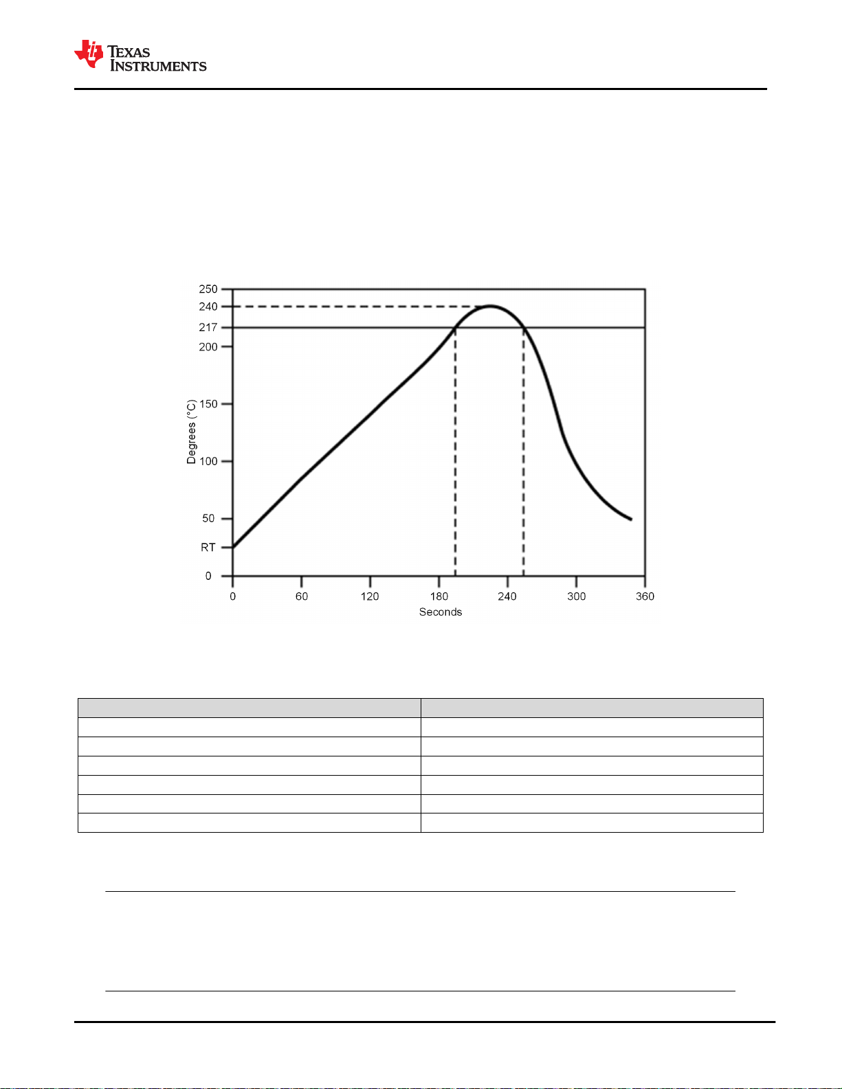
www.ti.com
CC3235MODS, CC3235MODSF, CC3235MODAS, CC3235MODASF
SWRS243A – FEBRUARY 2020 – REVISED MAY 2020
11.6 Soldering and Reflow Condition
• Heating method: Conventional convection or IR convection
• Temperature measurement: Thermocouple d = 0.1 mm to 0.2 mm CA (K) or CC (T) at soldering portion or
equivalent method
• Solder paste composition: SAC305
• Allowable reflow soldering times: 2 times based on the reflow soldering profile (see Figure 11-1)
• Temperature profile: Reflow soldering will be done according to the temperature profile (see
Figure 11-1)
• Peak temperature: 260°C
Figure 11-1. Temperature Profile for Evaluation of Solder Heat Resistance of a Component (at Solder
Joint)
Table 11-1. Temperature Profile
Profile Elements Convection or IR
Peak temperature range 235 to 240°C typical (260°C maximum)
Pre-heat / soaking (150 to 200°C) 60 to 120 seconds
Time above melting point 60 to 90 seconds
Time with 5°C to peak 30 seconds maximum
Ramp up < 3°C / second
Ramp down < -6°C / second
(1) For details, refer to the solder paste manufacturer's recommendation.
(1)
Note
TI does not recommend the use of conformal coating or similar material on the SimpleLink™ module.
This coating can lead to localized stress on the solder connections inside the module and impact the
module reliability. Use caution during the module assembly process to the final PCB to avoid the
presence of foreign material inside the module.
Copyright © 2020 Texas Instruments Incorporated
Product Folder Links: CC3235MODS CC3235MODSF CC3235MODAS CC3235MODASF
Submit Document Feedback
97

CC3235MODS, CC3235MODSF, CC3235MODAS, CC3235MODASF
SWRS243A – FEBRUARY 2020 – REVISED MAY 2020
www.ti.com
12 Device and Documentation Support
TI offers and extensive line of development tools. Tools and software to evaluate the performance of the device,
generate code, and develop solutions are listed in this section.
12.1 Development Tools and Software
For the most up to date list of Development Tools and Software, visit the CC3235MOD tools and software page.
Or, click on the Alert me button in the top-right corner of the page, to stay informed of updates related to the
CC3235MOD.
Pin Mux Tool
SimpleLink™ Wi-Fi
®
Starter Pro
SimpleLink™ CC32XX
Software Development
Kit (SDK)
The supported devices are: CC3200, CC3220x, and CC3235x.
The Pin Mux Tool is a software tool that provides a graphical user interface (GUI) for
configuring pin multiplexing settings, resolving conflicts and specifying I/O cell
characteristics for MPUs from TI. Results are output as C header/code files that can
be imported into software development kits (SDKs) or used to configure customers'
custom software. Version 3 of the Pin Mux Tool adds the capability of automatically
selecting a mux configuration that satisfies the entered requirements.
The supported devices are: CC3100, CC3200, CC3120R, CC3220x, CC3135, and
CC3235x.
The SimpleLink™ Wi-Fi® Starter Pro mobile App is a new mobile application for
SimpleLink™ provisioning. The app goes along with the embedded provisioning
library and example that runs on the device side (see SimpleLink™ Wi-Fi® SDK
plugin and TI SimpleLink™ CC32XX Software Development Kit (SDK)). The new
provisioning release is a TI recommendation for Wi-Fi® provisioning using
SimpleLink™ Wi-Fi® products. The provisioning release implements advanced AP
mode and SmartConfig™ technology provisioning with feedback and fallback options
to ensure successful process has been accomplished. Customers can use both
embedded library and the mobile library for integration to their end products.
The CC3235x devices are supported.
The SimpleLink™ CC32XX SDK contains drivers for the CC3235 programmable
MCU, more than 30 sample applications, and documentation needed to use the
solution. It also contains the flash programmer, a command line tool for flashing
software, configuring network and software parameters (SSID, access point channel,
network profile, BS NIEW), system files, and user files (certificates, web pages, and
more). This SDK can be used with TI’s SimpleLink™ Wi-Fi® CC3235 LaunchPad™
development kits.
Uniflash Standalone
Flash Tool for TI
Microcontrollers (MCU),
Sitara Processors &
SimpleLink Devices
SimpleLink™ Wi-Fi
®
Radio Testing Tool
98 Submit Document Feedback
Product Folder Links: CC3235MODS CC3235MODSF CC3235MODAS CC3235MODASF
The supported devices are: CC3120R, CC3220x, CC3135, and CC3235x.
CCS Uniflash is a standalone tool used to program on-chip flash memory on TI
MCUs and on-board flash memory for Sitara™ processors. Uniflash has a GUI,
command line, and scripting interface. CCS Uniflash is available free of charge.
The supported devices are: CC3100, CC3200, CC3120R, CC3220, CC3135, and
CC3235x.
The SimpleLink™ Wi-Fi® Radio Testing Tool is a Windows-based software tool for
RF evaluation and testing of SimpleLink™ Wi-Fi® CC3x20 and CC3x35 designs
during development and certification. The tool enables low-level radio testing
capabilities by manually setting the radio into transmit or receive modes. Using the
tool requires familiarity and knowledge of radio circuit theory and radio test methods.
Copyright © 2020 Texas Instruments Incorporated

X
PREFIX
X = preproduction device
CC 3235 MOD XXXX XXX R
DEVICE FAMILY
CC = wireless connectivity
SERIES NUMBER
3 = Wi-Fi
Centric
PACKAGE DESIGNATOR
MON = LGA package
PACKAGING
R = tape/reel
MODULE
MOD = module
SM2 = S module
SF12 = SF module
X
A = integral antenna
No prefix = no antenna
www.ti.com
CC3235MODS, CC3235MODSF, CC3235MODAS, CC3235MODASF
SWRS243A – FEBRUARY 2020 – REVISED MAY 2020
Created for the internet-of-things (IoT), the SimpleLink™ Wi-Fi® CC31xx and
CC32xx family of devices include on-chip Wi-Fi®, Internet, and robust security
protocols with no prior Wi-Fi® experience needed for faster development. For more
information on these devices, visit SimpleLink™ Wi-Fi® family, Internet-on-a chip™
solutions.
UniFlash Standalone
Flash Tool for TI
Microcontrollers (MCU),
CCS UniFlash is a standalone tool used to program on-chip flash memory on TI
MCUs and on-board flash memory for Sitara™ processors. UniFlash has a GUI,
command line, and scripting interface. CCS UniFlash is available free of charge.
Sitara™ Processors
and SimpleLink™
Devices
12.2 Firmware Updates
TI updates features in the service pack for this module with no published schedule. Due to the ongoing changes,
TI recommends users have the latest service pack in their module for production.
To stay informed, sign up for updates using the SDK Alert me button in the top-right corner of the product page,
or visit http://www.ti.com/tool/download/SIMPLELINK-CC32XX-SDK.
12.3 Device Nomenclature
To designate the stages in the product development cycle, TI assigns prefixes to the part numbers of the
CC3235MODx and CC3235MODAx and support tools (see Figure 12-1).
To designate the stages in the product development cycle, TI assigns prefixes to the part numbers of all
microprocessors (MPUs) and support tools. Each device has one of three prefixes: X, P, or null (no prefix) (for
example, CC3235MODxandCC3235MODAx). Texas Instruments recommends two of three possible prefix
designators for its support tools: TMDX and TMDS. These prefixes represent evolutionary stages of product
development from engineering prototypes (TMDX) through fully qualified production devices and tools (TMDS).
Device development evolutionary flow:
X Experimental device that is not necessarily representative of the final device's electrical specifications and
P Prototype device that is not necessarily the final silicon die and may not necessarily meet final electrical
null Production version of the silicon die that is fully qualified.
Support tool development evolutionary flow:
TMDX Development-support product that has not yet completed Texas Instruments internal qualification testing.
TMDS Fully-qualified development-support product.
Copyright © 2020 Texas Instruments Incorporated
may not use production assembly flow.
specifications.
Figure 12-1. CC3235MODx and CC3235MODAx Module Nomenclature
Product Folder Links: CC3235MODS CC3235MODSF CC3235MODAS CC3235MODASF
Submit Document Feedback
99

CC3235MODS, CC3235MODSF, CC3235MODAS, CC3235MODASF
SWRS243A – FEBRUARY 2020 – REVISED MAY 2020
www.ti.com
For orderable part numbers of the CC3235MODx and CC3235MODAx devices in the QFM package type, see
Section 13.2, see ti.com, or contact your TI sales representative.
12.4 Documentation Support
To receive notification of documentation updates — including silicon errata — go to the CC3235MOD product
folder on ti.com. In the upper-right corner, click on Alert me to receive a weekly digest of any product information
that has changed. For change details, check the revision history of any revised document.
The current documentation that describes the processor, related peripherals, and other technical collateral is as
follows.
Application Reports
CC3135 and CC3235 SimpleLink™
Wi-Fi® Embedded Programming
User Guide
SimpleLink™ CC3135, CC3235 WiFi® Internet-on-a chip™ Networking
Sub-System Power Management
SimpleLink™ CC31xx, CC32xx WiFi® Internet-on-a chip™ Solution
Built-In Security Features
SimpleLink™ CC3135, CC3235 WiFi® and Internet-of-Things Overthe-Air Update
SimpleLink™ CC3135, CC3235 WiFi® Internet-on-a chip™ Solution
Device Provisioning
Transfer of TI's Wi-Fi® Alliance
Certifications to Products Based
on SimpleLink™
Using Serial Flash on SimpleLink™
CC3135 and CC3235 Wi-Fi® and
Internet-of-Things Devices
CC3135 and CC3235 SimpleLink Wi-Fi Embedded Programming User
Guide
This application report describes the best practices for power
management and extended battery life for embedded low-power Wi-Fi
devices such as the SimpleLink Wi-Fi Internet-on-a chip solution from
Texas Instruments.
The SimpleLink Wi-Fi CC31xx and CC32xx Internet-on-a chip family of
devices from Texas Instruments offer a wide range of built-in security
features to help developers address a variety of security needs, which is
achieved without any processing burden on the main microcontroller
(MCU). This document describes these security-related features and
provides recommendations for leveraging each in the context of
practical system implementation.
This document describes the OTA library for the SimpleLink Wi-Fi
CC3x35 family of devices from Texas Instruments and explains how to
prepare a new cloud-ready update to be downloaded by the OTA library.
This guide describes the provisioning process, which provides the
SimpleLink Wi-Fi device with the information (network name, password,
and so forth) needed to connect to a wireless network.
This document explains how to employ the Wi-Fi® Alliance (WFA)
derivative certification transfer policy to transfer a WFA certification,
already obtained by Texas Instruments, to a system you have
developed.
This application note is divided into two parts. The first part provides
important guidelines and best- practice design techniques to consider
when choosing and embedding a serial Flash paired with the CC3135
and CC3235 (CC3x35) devices. The second part describes the file
system, along with guidelines and considerations for system designers
working with the CC3x35 devices.
More Literature
CC3235MODx SimpleLink™ Wi-Fi® and Internet-of-Things Hardware Design Files
CC3220MODAx SimpleLink™ Wi-Fi® and Internet-of-Things Hardware Design Files
CC3x35x SimpleLink™ Wi-Fi® and Internet-of-Things Design Checklist
User's Guides
CC3135 and CC3235
SimpleLink™ Wi-Fi
100 Submit Document Feedback
®
Product Folder Links: CC3235MODS CC3235MODSF CC3235MODAS CC3235MODASF
CC3135 and CC3235 SimpleLink Wi-Fi Embedded Programming User Guide
Copyright © 2020 Texas Instruments Incorporated
 Loading...