

Page 1

CC3200 SimpleLink Wi-Fi and Internet-ofThings Solution, a Single Chip Wireless MCU
Technical Reference Manual
Literature Number: SWRU367D
June 2014–Revised May 2018
Page 2

Contents
1 Architecture Overview......................................................................................................... 22
1.1 Introduction.................................................................................................................. 23
1.1.1 Related Documentation........................................................................................... 23
1.1.2 Register Bit Conventions ......................................................................................... 23
1.2 Architecture Overview ..................................................................................................... 24
1.3 Functional Overview ....................................................................................................... 25
1.3.1 Processor Core.................................................................................................... 25
1.3.2 Memory............................................................................................................. 26
1.3.3 Micro Direct Memory Access Controller (µDMA).............................................................. 27
1.3.4 General Purpose Timer (GPT) .................................................................................. 27
1.3.5 Watch Dog Timer (WDT)......................................................................................... 28
1.3.6 Multi-Channel Audio Serial Port (McASP) ..................................................................... 28
1.3.7 Serial Peripheral Interface (SPI)................................................................................. 28
1.3.8 Inter-Integrated Circuit Interface (I2C).......................................................................... 29
1.3.9 Universal Asynchronous Receiver/Transmitter (UART)...................................................... 29
1.3.10 General Purpose Input / Output (GPIO)....................................................................... 30
1.3.11 Analog to Digital Converter (ADC)............................................................................. 30
1.3.12 SD Card Host..................................................................................................... 30
1.3.13 Parallel Camera Interface....................................................................................... 30
1.3.14 Debug Interface .................................................................................................. 30
1.3.15 Hardware Cryptography Accelerator........................................................................... 31
1.3.16 Clock, Reset, and Power Management ....................................................................... 31
1.3.17 SimpleLink Subsystem .......................................................................................... 32
1.3.18 I/O Pads and Pin Multiplexing .................................................................................. 32
2 Cortex-M4 Processor .......................................................................................................... 33
2.1 Overview..................................................................................................................... 34
2.1.1 Block Diagram ..................................................................................................... 34
2.1.2 System-Level Interface ........................................................................................... 35
2.1.3 Integrated Configurable Debug.................................................................................. 35
2.1.4 Trace Port Interface Unit (TPIU) ................................................................................ 36
2.1.5 Cortex-M4 System Component Details......................................................................... 36
2.2 Functional Description ..................................................................................................... 36
2.2.1 Programming Model .............................................................................................. 36
2.2.2 Register Description .............................................................................................. 37
2.2.3 Memory Model..................................................................................................... 41
2.2.4 Exception Model................................................................................................... 44
2.2.5 Fault Handling ..................................................................................................... 50
2.2.6 Power Management............................................................................................... 52
2.2.7 Instruction Set Summary ......................................................................................... 54
3 Cortex-M4 Peripherals......................................................................................................... 59
3.1 Overview..................................................................................................................... 60
3.2 Functional Description ..................................................................................................... 60
3.2.1 System Timer (SysTick) .......................................................................................... 60
3.2.2 Nested Vectored Interrupt Controller (NVIC) .................................................................. 61
3.2.3 System Control Block (SCB)..................................................................................... 62
2
Contents
Copyright © 2014–2018, Texas Instruments Incorporated
SWRU367D–June 2014–Revised May 2018
Submit Documentation Feedback
Page 3

www.ti.com
3.3 Register Map................................................................................................................ 62
3.3.1 PERIPHERAL Registers ......................................................................................... 66
4 Direct Memory Access (DMA) .............................................................................................. 97
4.1 Overview..................................................................................................................... 98
4.2 Functional Description ..................................................................................................... 98
4.2.1 Channel Assignment.............................................................................................. 99
4.2.2 Priority............................................................................................................. 100
4.2.3 Arbitration Size................................................................................................... 100
4.2.4 Channel Configuration .......................................................................................... 100
4.2.5 Transfer Mode.................................................................................................... 101
4.2.6 Transfer Size and Increment................................................................................... 106
4.2.7 Peripheral Interface.............................................................................................. 107
4.2.8 Interrupts and Errors ............................................................................................ 107
4.3 Register Description...................................................................................................... 108
4.3.1 DMA Register Map .............................................................................................. 108
4.3.2 µDMA Channel Control Structure.............................................................................. 109
4.3.3 DMA Registers ................................................................................................... 110
4.3.4 DMA_(OFFSET_FROM_DMA_BASE_ADDRESS) Registers............................................. 115
5 General-Purpose Input/Outputs (GPIOs).............................................................................. 139
5.1 Overview................................................................................................................... 140
5.2 Functional Description.................................................................................................... 140
5.2.1 Data Control ...................................................................................................... 141
5.3 Interrupt Control........................................................................................................... 142
5.3.1 μDMA Trigger Source ........................................................................................... 142
5.4 Initialization and Configuration .......................................................................................... 142
5.5 GPIO_REGISTER_MAP Registers..................................................................................... 144
5.5.1 GPIO Register Description ..................................................................................... 144
6 Universal Asynchronous Receivers/Transmitters (UARTs) .................................................... 156
6.1 Overview................................................................................................................... 157
6.1.1 Block Diagram.................................................................................................... 158
6.2 Functional Description.................................................................................................... 158
6.2.1 Transmit/Receive Logic ......................................................................................... 158
6.2.2 Baud-Rate Generation .......................................................................................... 159
6.2.3 Data Transmission............................................................................................... 159
6.2.4 Initialization and Configuration ................................................................................. 162
6.3 Register Description...................................................................................................... 163
6.3.1 UART Registers.................................................................................................. 164
7 Inter-Integrated Circuit (I2C) Interface ................................................................................. 186
7.1 Overview................................................................................................................... 187
7.1.1 Block Diagram.................................................................................................... 188
7.1.2 Signal Description ............................................................................................... 188
7.2 Functional Description.................................................................................................... 189
7.2.1 I2C Bus Functional Overview .................................................................................. 189
7.2.2 Supported Speed Modes ....................................................................................... 193
7.2.3 Interrupts.......................................................................................................... 194
7.2.4 Loopback Operation............................................................................................. 194
7.2.5 FIFO and µDMA Operation..................................................................................... 194
7.2.6 Command Sequence Flow Charts............................................................................. 196
7.2.7 Initialization and Configuration ................................................................................. 203
7.3 Register Map .............................................................................................................. 204
7.3.1 I2C Registers..................................................................................................... 205
8 SPI (Serial Peripheral Interface).......................................................................................... 244
SWRU367D–June 2014–Revised May 2018
Submit Documentation Feedback
Copyright © 2014–2018, Texas Instruments Incorporated
Contents
3
Page 4

www.ti.com
8.1 Overview................................................................................................................... 245
8.1.1 Features........................................................................................................... 246
8.2 Functional Description.................................................................................................... 246
8.2.1 SPI interface...................................................................................................... 246
8.2.2 SPI Transmission ................................................................................................ 246
8.2.3 Master Mode ..................................................................................................... 250
8.2.4 Slave Mode....................................................................................................... 258
8.2.5 Interrupts.......................................................................................................... 260
8.2.6 DMA Requests ................................................................................................... 260
8.2.7 Reset .............................................................................................................. 261
8.3 Initialization and Configuration .......................................................................................... 261
8.3.1 Basic Initialization................................................................................................ 261
8.3.2 Master Mode Operation Without Interrupt (Polling) ......................................................... 261
8.3.3 Slave Mode Operation With Interrupt ......................................................................... 262
8.3.4 Generic Interrupt Handler Implementation ................................................................... 262
8.4 Access to Data Registers................................................................................................ 262
8.5 Module Initialization....................................................................................................... 263
8.5.1 Common Transfer Sequence................................................................................... 263
8.5.2 End of Transfer Sequences .................................................................................... 264
8.5.3 FIFO Mode........................................................................................................ 265
8.6 SPI Registers.............................................................................................................. 269
8.6.1 SPI Register Description........................................................................................ 270
9 General-Purpose Timers.................................................................................................... 285
9.1 Overview................................................................................................................... 286
9.2 Block Diagram............................................................................................................. 286
9.3 Functional Description.................................................................................................... 287
9.3.1 GPTM Reset Conditions ........................................................................................ 287
9.3.2 Timer Modes ..................................................................................................... 288
9.3.3 DMA Operation................................................................................................... 294
9.3.4 Accessing Concatenated 16/32-Bit GPTM Register Values ............................................... 294
9.4 Initialization and Configuration .......................................................................................... 294
9.4.1 One-Shot and Periodic Timer Mode........................................................................... 294
9.4.2 Input Edge-Count Mode......................................................................................... 295
9.4.3 Input Edge-Time Mode.......................................................................................... 295
9.4.4 PWM Mode ....................................................................................................... 296
9.5 TIMER Registers.......................................................................................................... 297
9.5.1 GPT Register Description....................................................................................... 297
10 Watchdog Timer ............................................................................................................... 327
10.1 Overview................................................................................................................... 328
10.1.1 Block Diagram................................................................................................... 328
10.2 Functional Description.................................................................................................... 329
10.2.1 Initialization and Configuration................................................................................ 329
10.3 Register Map .............................................................................................................. 329
10.3.1 Register Description............................................................................................ 330
10.4 MCU Watch Dog Controller Usage Caveats .......................................................................... 338
10.4.1 System WatchDog.............................................................................................. 338
10.4.2 System WatchDog Recovery Sequence..................................................................... 339
11 SD Host Controller Interface .............................................................................................. 341
11.1 Overview................................................................................................................... 342
11.2 SD Host Features......................................................................................................... 342
11.3 1-Bit SD Interface......................................................................................................... 343
11.3.1 Clock and Reset Management................................................................................ 343
11.4 Initialization and Configuration Using Peripheral APIs............................................................... 343
4
Contents
Copyright © 2014–2018, Texas Instruments Incorporated
SWRU367D–June 2014–Revised May 2018
Submit Documentation Feedback
Page 5

www.ti.com
11.4.1 Basic Initialization and Configuration......................................................................... 344
11.4.2 Sending Command ............................................................................................. 344
11.4.3 Card Detection and Initialization.............................................................................. 345
11.4.4 Block Read ...................................................................................................... 347
11.4.5 Block Write ...................................................................................................... 348
11.5 Performance and Testing................................................................................................ 348
11.6 Peripheral Library APIs .................................................................................................. 349
11.7 Register Description...................................................................................................... 353
11.7.1 SD-HOST Registers............................................................................................ 354
12 Inter-Integrated Sound (I2S) Multi-Channel Audio Serial Port................................................. 380
12.1 Overview................................................................................................................... 381
12.1.1 I2S Format....................................................................................................... 381
12.2 Functional Description.................................................................................................... 382
12.3 Programming Model...................................................................................................... 382
12.3.1 Clock and Reset Management................................................................................ 382
12.3.2 I2S Data Port Interface......................................................................................... 383
12.3.3 Initialization and Configuration................................................................................ 383
12.4 Peripheral Library APIs for I2S Configuration......................................................................... 385
12.4.1 Basic APIs for Enabling and Configuring the Interface .................................................... 385
12.4.2 APIs for Data Access if DMA is Not Used................................................................... 388
12.4.3 APIs for Setting Up, Handling Interrupts, or Getting Status from I2S Peripheral....................... 390
12.4.4 APIs to Control FIFO Structures Associated with I2S Peripheral ........................................ 394
13 Analog-to-Digital Converter [ADC] ...................................................................................... 396
13.1 Overview................................................................................................................... 397
13.2 Key Features .............................................................................................................. 397
13.3 ADC Register Mapping................................................................................................... 398
13.4 ADC_MODULE Registers ............................................................................................... 399
13.4.1 ADC Register Description ..................................................................................... 399
13.5 Initialization and Configuration ......................................................................................... 420
13.6 Peripheral Library APIs for ADC Operation ........................................................................... 421
13.6.1 Overview......................................................................................................... 421
13.6.2 Configuring the ADC Channels ............................................................................... 421
13.6.3 Basic APIs for Enabling and Configuring the Interface .................................................... 421
13.6.4 APIs for Data Transfer [Direct Access to FIFO and DMA Setup] ........................................ 422
13.6.5 APIs for Interrupt Usage ....................................................................................... 424
13.6.6 APIs for Setting Up ADC Timer for Time Stamping the Samples ........................................ 426
14 Parallel Camera Interface Module ....................................................................................... 428
14.1 Overview................................................................................................................... 429
14.2 Image Sensor Interface .................................................................................................. 429
14.3 Functional Description.................................................................................................... 430
14.3.1 Modes of Operation ............................................................................................ 430
14.3.2 FIFO Buffer ...................................................................................................... 432
14.3.3 Reset ............................................................................................................. 432
14.3.4 Clock Generation ............................................................................................... 433
14.3.5 Interrupt Generation ............................................................................................ 433
14.3.6 DMA Interface................................................................................................... 433
14.4 Programming Model...................................................................................................... 434
14.4.1 Camera Core Reset............................................................................................ 434
14.4.2 Enable the Picture Acquisition ................................................................................ 434
14.4.3 Disable the Picture Acquisition................................................................................ 435
14.5 Interrupt Handling......................................................................................................... 435
14.5.1 FIFO_OF_IRQ (FIFO overflow)............................................................................... 435
SWRU367D–June 2014–Revised May 2018
Submit Documentation Feedback
Copyright © 2014–2018, Texas Instruments Incorporated
Contents
5
Page 6

www.ti.com
14.5.2 FIFO_UF_IRQ (FIFO underflow) ............................................................................. 435
14.6 Camera Interface Module Functional Registers ...................................................................... 436
14.6.1 Functional Register Description............................................................................... 436
14.6.2 Peripheral Library APIs ........................................................................................ 447
14.7 Developer’s Guide ........................................................................................................ 450
14.7.1 Using Peripheral Driver APIs for Capturing an Image ..................................................... 450
14.7.2 Using Peripheral Driver APIs for Communicating with Image Sensors.................................. 452
15 Power, Reset and Clock Management ................................................................................. 454
15.1 Trademarks...................................................................................................................... 455
15.2 Overview................................................................................................................... 455
15.2.1 VBAT Wide-Voltage Connection.............................................................................. 455
15.2.2 Pre-Regulated 1.85 V.......................................................................................... 455
15.2.3 Supply Brownout and Blackout ............................................................................... 457
15.2.4 Application Processor Power Modes......................................................................... 457
15.3 Power Management Control Architecture ............................................................................. 459
15.3.1 Global Power-Reset-Clock Manager (GPRCM) ............................................................ 461
15.3.2 Application Reset-Clock Manager (ARCM) ................................................................. 462
15.4 PRCM APIs................................................................................................................ 462
15.4.1 MCU Initialization ............................................................................................... 462
15.4.2 Reset Control.................................................................................................... 462
15.4.3 Peripheral Reset ................................................................................................ 462
15.4.4 Reset Cause..................................................................................................... 462
15.4.5 Clock Control.................................................................................................... 463
15.4.6 Low Power Modes.............................................................................................. 463
15.4.7 Sleep (SLEEP) .................................................................................................. 464
15.4.8 Deep Sleep (DEEPSLEEP) ................................................................................... 464
15.4.9 Low-Power Deep Sleep (LPDS) .............................................................................. 464
15.4.10 Hibernate (HIB)................................................................................................ 466
15.4.11 Slow Clock Counter........................................................................................... 468
15.5 Peripheral Macros ........................................................................................................ 468
15.6 Power Management Framework........................................................................................ 469
15.7 PRCM Registers .......................................................................................................... 470
15.7.1 PRCM Register Description................................................................................... 471
16 I/O Pads and Pin Multiplexing............................................................................................. 522
16.1 Overview................................................................................................................... 523
16.2 I/O Pad Electrical Specifications........................................................................................ 523
16.3 Analog-Digital Pin Multiplexing.......................................................................................... 525
16.4 Special Ana/DIG Pins .................................................................................................... 526
16.4.1 Pin 45 and 52 ................................................................................................... 526
16.4.2 Pin 29 and 30 ................................................................................................... 528
16.4.3 Pin 57, 58, 59, 60............................................................................................... 528
16.5 Analog Mux Control Registers .......................................................................................... 528
16.6 Pins Available for Applications.......................................................................................... 530
16.7 Functional Pin Mux Configurations..................................................................................... 532
16.8 Pin Mapping Recommendations........................................................................................ 546
16.8.1 Pad Configuration Registers for Application Pins .......................................................... 547
16.8.2 PAD Behavior During Reset and Hibernate................................................................. 549
16.8.3 Control Architecture ............................................................................................ 549
16.8.4 CC3200 Pin-mux Examples................................................................................... 550
16.8.5 Wake on Pad.................................................................................................... 553
16.8.6 Sense on Power ................................................................................................ 553
A Software Development Kit Examples................................................................................... 556
6
Contents
Copyright © 2014–2018, Texas Instruments Incorporated
SWRU367D–June 2014–Revised May 2018
Submit Documentation Feedback
Page 7

www.ti.com
A.1 Software Development Kit Examples .................................................................................. 556
B CC3200 Miscellaneous Registers........................................................................................ 557
B.1 Miscellaneous Register Summary ...................................................................................... 557
B.1.1 DMA_IMR Register (offset = 8Ch) [reset = FF0Fh] ......................................................... 558
B.1.2 DMA_IMS Register (offset = 90h) [reset = 0h]............................................................... 560
B.1.3 DMA_IMC Register (offset = 94h) [reset = 0h]............................................................... 562
B.1.4 DMA_ICR Register (offset = 9Ch) [reset = 0h] .............................................................. 564
B.1.5 DMA_MIS Register (offset = A0h) [reset = 0h] .............................................................. 566
B.1.6 DMA_RIS Register (offset = A4h) [reset = 0h]............................................................... 568
B.1.7 GPTTRIGSEL Register (offset = B0h) [reset = 0h].......................................................... 570
Revision History ........................................................................................................................ 571
SWRU367D–June 2014–Revised May 2018
Submit Documentation Feedback
Copyright © 2014–2018, Texas Instruments Incorporated
Contents
7
Page 8

www.ti.com
List of Figures
1-1. CC3200 MCU and WIFI System-on-Chip............................................................................... 24
2-1. Application CPU Block Diagram.......................................................................................... 35
2-2. TPIU Block Diagram ....................................................................................................... 36
2-3. Cortex-M4 Register Set ................................................................................................... 38
2-4. Data Storage................................................................................................................ 43
2-5. Vector Table ................................................................................................................ 48
2-6. Exception Stack Frame.................................................................................................... 50
2-7. Power Management Architecture in CC3200 SoC..................................................................... 53
3-1. ACTLR Register ............................................................................................................ 67
3-2. STCTRL Register .......................................................................................................... 68
3-3. STRELOAD Register ...................................................................................................... 69
3-4. STCURRENT Register .................................................................................................... 70
3-5. EN_0 to EN_6 Register.................................................................................................... 71
3-6. DIS_0 to DIS_6 Register.................................................................................................. 72
3-7. PEND_0 to PEND_6 Register............................................................................................ 73
3-8. UNPEND_0 to UNPEND_6 Register .................................................................................... 74
3-9. ACTIVE_0 to ACTIVE_6 Register........................................................................................ 75
3-10. PRI_0 to PRI_49 Register................................................................................................. 76
3-11. CPUID Register............................................................................................................. 77
3-12. INTCTRL Register.......................................................................................................... 78
3-13. VTABLE Register........................................................................................................... 80
3-14. APINT Register ............................................................................................................. 81
3-15. SYSCTRL Register ........................................................................................................ 82
3-16. CFGCTRL Register ........................................................................................................ 83
3-17. SYSPRI1 Register.......................................................................................................... 85
3-18. SYSPRI2 Register.......................................................................................................... 86
3-19. SYSPRI3 Register.......................................................................................................... 87
3-20. SYSHNDCTRL Register................................................................................................... 88
3-21. FAULTSTAT Register ..................................................................................................... 90
3-22. HFAULTSTAT Register.................................................................................................... 94
3-23. FAULTDDR Register....................................................................................................... 95
3-24. SWTRIG Register .......................................................................................................... 96
4-1. DMA Channel Assignment ................................................................................................ 99
4-2. Ping-Pong Mode .......................................................................................................... 103
4-3. Memory Scatter-Gather Mode .......................................................................................... 105
4-4. Peripheral Scatter-Gather Mode........................................................................................ 106
4-5. DMA_SRCENDP Register............................................................................................... 111
4-6. DMA_DSTENDP Register ............................................................................................... 112
4-7. DMA_CHCTL Register................................................................................................... 113
4-8. DMA_STAT Register ..................................................................................................... 116
4-9. DMA_CFG Register ...................................................................................................... 117
4-10. DMA_CTLBASE Register................................................................................................ 118
4-11. DMA_ALTBASE Register................................................................................................ 119
4-12. DMA_WAITSTAT Register .............................................................................................. 120
4-13. DMA_SWREQ Register.................................................................................................. 121
4-14. DMA_USEBURSTSET Register ........................................................................................ 122
4-15. DMA_USEBURSTCLR Register........................................................................................ 123
8
List of Figures
Copyright © 2014–2018, Texas Instruments Incorporated
SWRU367D–June 2014–Revised May 2018
Submit Documentation Feedback
Page 9

www.ti.com
4-16. DMA_REQMASKSET Register ......................................................................................... 124
4-17. DMA_REQMASKCLR Register ......................................................................................... 125
4-18. DMA_ENASET Register ................................................................................................. 126
4-19. DMA_ENACLR Register ................................................................................................. 127
4-20. DMA_ALTSET Register.................................................................................................. 128
4-21. DMA_ALTCLR Register.................................................................................................. 129
4-22. DMA_PRIOSET Register ................................................................................................ 130
4-23. DMA_PRIOCLR Register................................................................................................ 131
4-24. DMA_ERRCLR Register................................................................................................. 132
4-25. DMA_CHASGN Register ................................................................................................ 133
4-26. DMA_CHMAP0 Register................................................................................................. 134
4-27. DMA_CHMAP1 Register................................................................................................. 135
4-28. DMA_CHMAP2 Register................................................................................................. 136
4-29. DMA_CHMAP3 Register................................................................................................. 137
4-30. DMA_PV Register ........................................................................................................ 138
5-1. Digital I/O Pads ........................................................................................................... 140
5-2. GPIODATA Write Example.............................................................................................. 141
5-3. GPIODATA Read Example.............................................................................................. 141
5-4. GPIODATA Register ..................................................................................................... 145
5-5. GPIODIR Register ........................................................................................................ 146
5-6. GPIOIS Register .......................................................................................................... 147
5-7. GPIOIBE Register ........................................................................................................ 148
5-8. GPIOIEV Register ........................................................................................................ 149
5-9. GPIOIM Register.......................................................................................................... 150
5-10. GPIORIS Register ........................................................................................................ 151
5-11. GPIOMIS Register........................................................................................................ 152
5-12. GPIOICR Register ........................................................................................................ 153
6-1. UART Module Block Diagram........................................................................................... 158
6-2. UART Character Frame.................................................................................................. 159
6-3. UARTDR Register ........................................................................................................ 165
6-4. UARTRSR_UARTECR Register........................................................................................ 166
6-5. UARTFR Register ........................................................................................................ 168
6-6. UARTFBRD Register..................................................................................................... 171
6-7. UARTLCRH Register..................................................................................................... 172
6-8. UARTCTL Register....................................................................................................... 174
6-9. UARTIFLS Register ...................................................................................................... 176
6-10. UARTIM Register ......................................................................................................... 177
6-11. UARTRIS Register........................................................................................................ 179
6-12. UARTMIS Register ....................................................................................................... 181
6-13. UARTICR Register ....................................................................................................... 183
6-14. UARTDMACTL Register ................................................................................................. 185
7-1. I2C Block Diagram........................................................................................................ 188
7-2. I2C Bus Configuration.................................................................................................... 189
7-3. START and STOP Conditions .......................................................................................... 190
7-4. Complete Data Transfer with a 7-Bit Address ........................................................................ 190
7-5. R/S Bit in First Byte....................................................................................................... 190
7-6. Data Validity During Bit Transfer on the I2C Bus..................................................................... 191
7-7. Master Single TRANSMIT ............................................................................................... 197
7-8. Master Single RECEIVE ................................................................................................. 198
SWRU367D–June 2014–Revised May 2018
Submit Documentation Feedback
Copyright © 2014–2018, Texas Instruments Incorporated
List of Figures
9
Page 10

www.ti.com
7-9. Master TRANSMIT of Multiple Data Bytes ............................................................................ 199
7-10. Master RECEIVE of Multiple Data Bytes .............................................................................. 200
7-11. Master RECEIVE with Repeated START after Master TRANSMIT................................................ 201
7-12. Master TRANSMIT with Repeated START after Master RECEIVE................................................ 202
7-13. Slave Command Sequence ............................................................................................. 203
7-14. I2CMSA Register ......................................................................................................... 206
7-15. I2CMCS Register ......................................................................................................... 207
7-16. I2CMDR Register ......................................................................................................... 209
7-17. I2CMTPR Register........................................................................................................ 210
7-18. I2CMIMR Register ........................................................................................................ 211
7-19. I2CMRIS Register ........................................................................................................ 213
7-20. I2CMMIS Register ........................................................................................................ 215
7-21. I2CMICR Register ........................................................................................................ 217
7-22. I2CMCR Register ......................................................................................................... 219
7-23. I2CMCLKOCNT Register ................................................................................................ 220
7-24. I2CMBMON Register..................................................................................................... 221
7-25. I2CMBLEN Register...................................................................................................... 222
7-26. I2CMBCNT Register...................................................................................................... 223
7-27. I2CSOAR Register........................................................................................................ 224
7-28. I2CSCSR Register........................................................................................................ 225
7-29. I2CSDR Register.......................................................................................................... 227
7-30. I2CSIMR Register ........................................................................................................ 228
7-31. I2CSRIS Register......................................................................................................... 230
7-32. I2CSMIS Register......................................................................................................... 232
7-33. I2CSICR Register......................................................................................................... 234
7-34. I2CSOAR2 Register ...................................................................................................... 236
7-35. I2CSACKCTL Register................................................................................................... 237
7-36. I2CFIFODATA Register.................................................................................................. 238
7-37. I2CFIFOCTL Register .................................................................................................... 239
7-38. I2CFIFOSTATUS Register .............................................................................................. 241
7-39. I2CPP Register............................................................................................................ 242
7-40. I2CPC Register ........................................................................................................... 243
8-1. SPI Block Diagram........................................................................................................ 245
8-2. SPI Full Duplex Transmission (Example).............................................................................. 247
8-3. Full Duplex Single Transfer Format with PHA = 0.................................................................... 249
8-4. Full Duplex Single Transfer Format with PHA = 1.................................................................... 250
8-5. Contiguous Transfers with SPIEN Kept Active (2 Data Pins Interface Mode).................................... 252
8-6. Transmit/Receive Mode With no FIFO Used.......................................................................... 254
8-7. Transmit/Receive Mode With Only Receive FIFO Enabled......................................................... 254
8-8. Transmit/Receive Mode With Only Transmit FIFO Used............................................................ 255
8-9. Transmit/Receive Mode With Both FIFO Directions Used .......................................................... 255
8-10. Buffer Almost Full Level (AFL) .......................................................................................... 256
8-11. Buffer Almost Empty Level (AEL)....................................................................................... 256
8-12. 3-Pin Mode System Overview........................................................................................... 257
8-13. Flow Chart - Module Initialization....................................................................................... 263
8-14. Flow Chart - Common Transfer Sequence............................................................................ 264
8-15. Flow Chart - Transmit and Receive (Master and Slave)............................................................. 265
8-16. Flow Chart - FIFO Mode Common Sequence (Master) ............................................................. 267
8-17. Flow Chart - FIFO Mode Transmit and Receive with Word Count (Master)...................................... 268
10
List of Figures
Copyright © 2014–2018, Texas Instruments Incorporated
SWRU367D–June 2014–Revised May 2018
Submit Documentation Feedback
Page 11

www.ti.com
8-18. Flow Chart - FIFO Mode Transmit and Receive without Word Count (Master) .................................. 269
8-19. SPI_SYSCONFIG Register.............................................................................................. 271
8-20. SPI_SYSSTATUS Register.............................................................................................. 272
8-21. SPI_IRQSTATUS Register .............................................................................................. 273
8-22. SPI_IRQENABLE Register .............................................................................................. 275
8-23. SPI_MODULCTRL Register............................................................................................. 276
8-24. SPI_CHCONF Register .................................................................................................. 277
8-25. SPI_CHSTAT Register................................................................................................... 280
8-26. SPI_CHCTRL Register................................................................................................... 281
8-27. SPI_TX Register .......................................................................................................... 282
8-28. SPI_RX Register.......................................................................................................... 283
8-29. SPI_XFERLEVEL Register .............................................................................................. 284
9-1. GPTM Module Block Diagram .......................................................................................... 286
9-2. Input Edge-Count Mode Example, Counting Down .................................................................. 291
9-3. 16-Bit Input Edge-Time Mode Example................................................................................ 292
9-4. 16-Bit PWM Mode Example............................................................................................. 293
9-5. GPTMCFG Register...................................................................................................... 298
9-6. GPTMTAMR Register.................................................................................................... 299
9-7. GPTMTBMR Register.................................................................................................... 301
9-8. GPTMCTL Register....................................................................................................... 303
9-9. GPTMIMR Register....................................................................................................... 305
9-10. GPTMRIS Register ....................................................................................................... 307
9-11. GPTMMIS Register....................................................................................................... 309
9-12. GPTMICR Register ....................................................................................................... 311
9-13. GPTMTAILR Register .................................................................................................... 313
9-14. GPTMTBILR Register .................................................................................................... 314
9-15. GPTMTAMATCHR Register............................................................................................. 315
9-16. GPTMTBMATCHR Register............................................................................................. 316
9-17. GPTMTAPR Register .................................................................................................... 317
9-18. GPTMTBPR Register .................................................................................................... 318
9-19. GPTMTAPMR Register .................................................................................................. 319
9-20. GPTMTBPMR Register .................................................................................................. 320
9-21. GPTMTAR Register ...................................................................................................... 321
9-22. GPTMTBR Register ...................................................................................................... 322
9-23. GPTMTAV Register ...................................................................................................... 323
9-24. GPTMTBV Register ...................................................................................................... 324
9-25. GPTMDMAEV Register .................................................................................................. 325
10-1. WDT Module Block Diagram ............................................................................................ 328
10-2. WDTLOAD Register...................................................................................................... 332
10-3. WDTVALUE Register .................................................................................................... 333
10-4. WDTCTL Register ........................................................................................................ 334
10-5. WDTICR Register......................................................................................................... 335
10-6. WDTRIS Register......................................................................................................... 336
10-7. WDTTEST Register ...................................................................................................... 337
10-8. WDTLOCK Register...................................................................................................... 338
10-9. WatchDog Flow Chart.................................................................................................... 339
10-10. System WatchDog Recovery Sequence............................................................................... 340
11-1. SDHost Controller Interface Block Diagram........................................................................... 343
11-2. MMCHS_CSRE Register ................................................................................................ 355
SWRU367D–June 2014–Revised May 2018
Submit Documentation Feedback
Copyright © 2014–2018, Texas Instruments Incorporated
List of Figures
11
Page 12

www.ti.com
11-3. MMCHS_CON Register.................................................................................................. 356
11-4. MMCHS_BLK Register................................................................................................... 358
11-5. MMCHS_ARG Register.................................................................................................. 359
11-6. MMCHS_CMD Register.................................................................................................. 360
11-7. MMCHS_RSP10 Register ............................................................................................... 362
11-8. MMCHS_RSP32 Register ............................................................................................... 363
11-9. MMCHS_RSP54 Register ............................................................................................... 364
11-10. MMCHS_RSP76 Register ............................................................................................... 365
11-11. MMCHS_DATA Register................................................................................................. 366
11-12. MMCHS_PSTATE Register ............................................................................................. 367
11-13. MMCHS_HCTL Register................................................................................................. 369
11-14. MMCHS_SYSCTL Register ............................................................................................. 370
11-15. MMCHS_STAT Register................................................................................................. 372
11-16. MMCHS_IE Register ..................................................................................................... 376
11-17. MMCHS_ISE Register ................................................................................................... 378
12-1. I2S Protocol................................................................................................................ 381
12-2. MCASP Module ........................................................................................................... 382
12-3. Logical Clock Path........................................................................................................ 383
13-1. Architecture of the ADC Module in CC3200 .......................................................................... 397
13-2. Operation of the ADC .................................................................................................... 398
13-3. ADC_CTRL Register ..................................................................................................... 400
13-4. ADC_CH0_IRQ_EN Register ........................................................................................... 401
13-5. ADC_CH2_IRQ_EN Register ........................................................................................... 402
13-6. ADC_CH4_IRQ_EN Register ........................................................................................... 403
13-7. ADC_CH6_IRQ_EN Register ........................................................................................... 404
13-8. ADC_CH0_IRQ_STATUS Register .................................................................................... 405
13-9. ADC_CH2_IRQ_STATUS Register .................................................................................... 406
13-10. ADC_CH4_IRQ_STATUS Register .................................................................................... 407
13-11. ADC_CH6_IRQ_STATUS Register .................................................................................... 408
13-12. ADC_DMA_MODE_EN Register ....................................................................................... 409
13-13. ADC_TIMER_CONFIGURATION Register............................................................................ 410
13-14. ADC_TIMER_CURRENT_COUNT Register .......................................................................... 411
13-15. CHANNEL0FIFODATA Register........................................................................................ 412
13-16. CHANNEL2FIFODATA Register........................................................................................ 413
13-17. CHANNEL4FIFODATA Register........................................................................................ 414
13-18. CHANNEL6FIFODATA Register........................................................................................ 415
13-19. ADC_CH0_FIFO_LVL Register......................................................................................... 416
13-20. ADC_CH2_FIFO_LVL Register......................................................................................... 417
13-21. ADC_CH4_FIFO_LVL Register......................................................................................... 418
13-22. ADC_CH6_FIFO_LVL Register......................................................................................... 419
13-23. ADC_CH_ENABLE Register ............................................................................................ 420
14-1. The Camera Module Interfaces......................................................................................... 429
14-2. Synchronization Signals and Frame Timing........................................................................... 430
14-3. Synchronization Signals and Data Timing............................................................................. 430
14-4. Different Scenarios of CAM_P_HS and CAM_P_VS ................................................................ 431
14-5. CAM_P_HS Toggles Between Pixels in Decimation................................................................. 431
14-6. Parallel Camera I/F State Machine..................................................................................... 431
14-7. FIFO Image Data Format................................................................................................ 432
14-8. Assertion and De-Assertion of the DMA Request Signal............................................................ 434
12
List of Figures
Copyright © 2014–2018, Texas Instruments Incorporated
SWRU367D–June 2014–Revised May 2018
Submit Documentation Feedback
Page 13

www.ti.com
14-9. CC_SYSCONFIG Register .............................................................................................. 437
14-10. CC_SYSSTATUS Register.............................................................................................. 438
14-11. CC_IRQSTATUS Register............................................................................................... 439
14-12. CC_IRQENABLE Register............................................................................................... 441
14-13. CC_CTRL Register....................................................................................................... 443
14-14. CC_CTRL_DMA Register ............................................................................................... 445
14-15. CC_CTRL_XCLK Register .............................................................................................. 446
14-16. CC_FIFODATA Register................................................................................................. 447
15-1. Power Management Unit Supports Two Supply Configurations.................................................... 456
15-2. Sleep Modes .............................................................................................................. 459
15-3. Power Management Control Architecture in CC3200................................................................ 461
15-4. CAMCLKCFG Register .................................................................................................. 472
15-5. CAMCLKEN Register .................................................................................................... 473
15-6. CAMSWRST Register.................................................................................................... 474
15-7. MCASPCLKEN Register................................................................................................. 475
15-8. MCASPSWRST Register ................................................................................................ 476
15-9. SDIOMCLKCFG Register................................................................................................ 477
15-10. SDIOMCLKEN Register.................................................................................................. 478
15-11. SDIOMSWRST Register................................................................................................. 479
15-12. APSPICLKCFG Register................................................................................................. 480
15-13. APSPICLKEN Register .................................................................................................. 481
15-14. APSPISWRST Register.................................................................................................. 482
15-15. DMACLKEN Register .................................................................................................... 483
15-16. DMASWRST Register.................................................................................................... 484
15-17. GPIO0CLKEN Register .................................................................................................. 485
15-18. GPIO0SWRST Register ................................................................................................. 486
15-19. GPIO1CLKEN Register .................................................................................................. 487
15-20. GPIO1SWRST Register ................................................................................................. 488
15-21. GPIO2CLKEN Register .................................................................................................. 489
15-22. GPIO2SWRST Register ................................................................................................. 490
15-23. GPIO3CLKEN Register .................................................................................................. 491
15-24. GPIO3SWRST Register ................................................................................................. 492
15-25. GPIO4CLKEN Register .................................................................................................. 493
15-26. GPIO4SWRST Register ................................................................................................. 494
15-27. WDTCLKEN Register .................................................................................................... 495
15-28. WDTSWRST Register.................................................................................................... 496
15-29. UART0CLKEN Register.................................................................................................. 497
15-30. UART0SWRST Register................................................................................................. 498
15-31. UART1CLKEN Register.................................................................................................. 499
15-32. UART1SWRST Register................................................................................................. 500
15-33. GPT0CLKCFG Register ................................................................................................. 501
15-34. GPT0SWRST Register................................................................................................... 502
15-35. GPT1CLKEN Register ................................................................................................... 503
15-36. GPT1SWRST Register................................................................................................... 504
15-37. GPT2CLKEN Register ................................................................................................... 505
15-38. GPT2SWRST Register................................................................................................... 506
15-39. GPT3CLKEN Register ................................................................................................... 507
15-40. GPT3SWRST Register................................................................................................... 508
15-41. MCASPCLKCFG0 Register ............................................................................................. 509
SWRU367D–June 2014–Revised May 2018
Submit Documentation Feedback
Copyright © 2014–2018, Texas Instruments Incorporated
List of Figures
13
Page 14

www.ti.com
15-42. MCASPCLKCFG1 Register ............................................................................................. 510
15-43. I2CLCKEN Register ...................................................................................................... 511
15-44. I2CSWRST Register ..................................................................................................... 512
15-45. LPDSREQ Register....................................................................................................... 513
15-46. TURBOREQ Register .................................................................................................... 514
15-47. DSLPWAKECFG Register............................................................................................... 515
15-48. DSLPTIMRCFG Register ................................................................................................ 516
15-49. SLPWAKEEN Register................................................................................................... 517
15-50. SLPTMRCFG Register................................................................................................... 518
15-51. WAKENWP Register ..................................................................................................... 519
15-52. RCM_IS Register ......................................................................................................... 520
15-53. RCM_IEN Register ....................................................................................................... 521
16-1. Board Configuration to Use Pins 45 and 52 as Digital Signals..................................................... 526
16-2. Board Configuration to Use Pins 45 and 52 as Digital Signals..................................................... 527
16-3. I/O Pad Data and Control Path Architecture in CC3200............................................................. 550
16-4. Wake on Pad for Hibernate Mode...................................................................................... 553
B-1. DMA_IMR Register....................................................................................................... 558
B-2. DMA_IMS Register ....................................................................................................... 560
B-3. DMA_IMC Register....................................................................................................... 562
B-4. DMA_ICR Register ....................................................................................................... 564
B-5. DMA_MIS Register ....................................................................................................... 566
B-6. DMA_RIS Register ....................................................................................................... 568
B-7. GPTTRIGSEL Register .................................................................................................. 570
14
List of Figures
Copyright © 2014–2018, Texas Instruments Incorporated
SWRU367D–June 2014–Revised May 2018
Submit Documentation Feedback
Page 15

www.ti.com
1-1. Register Bit Accessibility and Initial Condition ......................................................................... 23
2-1. Summary of Processor Mode, Privilege Level, and Stack Use ...................................................... 37
2-2. Processor Register Map................................................................................................... 38
2-3. PSR Register Combinations .............................................................................................. 40
2-4. Memory Map................................................................................................................ 41
2-5. SRAM Memory Bit-Banding Regions.................................................................................... 42
2-6. Exception Types............................................................................................................ 46
2-7. CC3200 Application Processor Interrupts............................................................................... 46
2-8. Faults ........................................................................................................................ 50
2-9. Fault Status and Fault Address Registers .............................................................................. 52
2-10. Cortex-M4 Instruction Summary.......................................................................................... 54
3-1. Core Peripheral Register Regions ....................................................................................... 60
3-2. Peripherals Register Map ................................................................................................. 62
3-3. PERIPHERAL REGISTERS .............................................................................................. 66
3-4. ACTLR Register Field Descriptions...................................................................................... 67
3-5. STCTRL Register Field Descriptions .................................................................................... 68
3-6. STRELOAD Register Field Descriptions................................................................................ 69
3-7. STCURRENT Register Field Descriptions.............................................................................. 70
3-8. EN_0 to EN_6 Register Field Descriptions ............................................................................. 71
3-9. DIS_0 to DIS_6 Register Field Descriptions............................................................................ 72
3-10. PEND_0 to PEND_6 Register Field Descriptions...................................................................... 73
3-11. UNPEND_0 to UNPEND_6 Register Field Descriptions.............................................................. 74
3-12. ACTIVE_0 to ACTIVE_6 Register Field Descriptions ................................................................. 75
3-13. PRI_0 to PRI_49 Register Field Descriptions .......................................................................... 76
3-14. CPUID Register Field Descriptions ...................................................................................... 77
3-15. INTCTRL Register Field Descriptions ................................................................................... 78
3-16. VTABLE Register Field Descriptions .................................................................................... 80
3-17. APINT Register Field Descriptions....................................................................................... 81
3-18. SYSCTRL Register Field Descriptions .................................................................................. 82
3-19. CFGCTRL Register Field Descriptions.................................................................................. 83
3-20. SYSPRI1 Register Field Descriptions ................................................................................... 85
3-21. SYSPRI2 Register Field Descriptions ................................................................................... 86
3-22. SYSPRI3 Register Field Descriptions ................................................................................... 87
3-23. SYSHNDCTRL Register Field Descriptions ............................................................................ 88
3-24. FAULTSTAT Register Field Descriptions ............................................................................... 90
3-25. HFAULTSTAT Register Field Descriptions ............................................................................. 94
3-26. FAULTDDR Register Field Descriptions ................................................................................ 95
3-27. SWTRIG Register Field Descriptions.................................................................................... 96
4-1. Channel Control Memory ................................................................................................ 100
4-2. Individual Control Structure.............................................................................................. 101
4-3. 8-bit Data Peripheral Configuration..................................................................................... 106
4-4. µDMA Register Map...................................................................................................... 108
4-5. DMA Registers ............................................................................................................ 110
4-6. DMA_SRCENDP Register Field Descriptions ........................................................................ 111
4-7. DMA_DSTENDP Register Field Descriptions......................................................................... 112
4-8. DMA_CHCTL Register Field Descriptions............................................................................. 113
4-9. DMA_(OFFSET_FROM_DMA_BASE_ADDRESS) Registers...................................................... 115
List of Tables
SWRU367D–June 2014–Revised May 2018
Submit Documentation Feedback
Copyright © 2014–2018, Texas Instruments Incorporated
List of Tables
15
Page 16

www.ti.com
4-10. DMA_STAT Register Field Descriptions............................................................................... 116
4-11. DMA_CFG Register Field Descriptions................................................................................ 117
4-12. DMA_CTLBASE Register Field Descriptions ......................................................................... 118
4-13. DMA_ALTBASE Register Field Descriptions ......................................................................... 119
4-14. DMA_WAITSTAT Register Field Descriptions........................................................................ 120
4-15. DMA_SWREQ Register Field Descriptions ........................................................................... 121
4-16. DMA_USEBURSTSET Register Field Descriptions.................................................................. 122
4-17. DMA_USEBURSTCLR Register Field Descriptions.................................................................. 123
4-18. DMA_REQMASKSET Register Field Descriptions................................................................... 124
4-19. DMA_REQMASKCLR Register Field Descriptions................................................................... 125
4-20. DMA_ENASET Register Field Descriptions........................................................................... 126
4-21. DMA_ENACLR Register Field Descriptions........................................................................... 127
4-22. DMA_ALTSET Register Field Descriptions ........................................................................... 128
4-23. DMA_ALTCLR Register Field Descriptions ........................................................................... 129
4-24. DMA_PRIOSET Register Field Descriptions.......................................................................... 130
4-25. DMA_PRIOCLR Register Field Descriptions.......................................................................... 131
4-26. DMA_ERRCLR Register Field Descriptions........................................................................... 132
4-27. DMA_CHASGN Register Field Descriptions .......................................................................... 133
4-28. DMA_CHMAP0 Register Field Descriptions .......................................................................... 134
4-29. DMA_CHMAP1 Register Field Descriptions .......................................................................... 135
4-30. DMA_CHMAP2 Register Field Descriptions .......................................................................... 136
4-31. DMA_CHMAP3 Register Field Descriptions .......................................................................... 137
4-32. DMA_PV Register Field Descriptions.................................................................................. 138
5-1. GPIO Pad Configuration Examples .................................................................................... 142
5-2. GPIO Interrupt Configuration Example................................................................................. 143
5-3. GPIO_REGISTER_MAP Registers..................................................................................... 144
5-4. GPIODATA Register Field Descriptions ............................................................................... 145
5-5. GPIODIR Register Field Descriptions.................................................................................. 146
5-6. GPIOIS Register Field Descriptions.................................................................................... 147
5-7. GPIOIBE Register Field Descriptions.................................................................................. 148
5-8. GPIOIEV Register Field Descriptions.................................................................................. 149
5-9. GPIOIM Register Field Descriptions ................................................................................... 150
5-10. GPIORIS Register Field Descriptions.................................................................................. 151
5-11. GPIOMIS Register Field Descriptions.................................................................................. 152
5-12. GPIOICR Register Field Descriptions.................................................................................. 153
5-13. GPIO_TRIG_EN Register Field Descriptions ......................................................................... 154
5-14. GPIO Mapping ............................................................................................................ 154
6-1. Flow Control Mode........................................................................................................ 160
6-2. UART Register Map ...................................................................................................... 163
6-3. UART REGISTERS....................................................................................................... 164
6-4. UARTDR Register Field Descriptions.................................................................................. 165
6-5. UARTRSR_UARTECR Register Field Descriptions.................................................................. 166
6-6. UARTFR Register Field Descriptions .................................................................................. 168
6-7. UARTIBRD Register Field Descriptions ............................................................................... 170
6-8. UARTFBRD Register Field Descriptions .............................................................................. 171
6-9. UARTLCRH Register Field Descriptions .............................................................................. 172
6-10. UARTCTL Register Field Descriptions................................................................................. 174
6-11. UARTIFLS Register Field Descriptions ................................................................................ 176
6-12. UARTIM Register Field Descriptions................................................................................... 177
16
List of Tables
Copyright © 2014–2018, Texas Instruments Incorporated
SWRU367D–June 2014–Revised May 2018
Submit Documentation Feedback
Page 17

www.ti.com
6-13. UARTRIS Register Field Descriptions ................................................................................. 179
6-14. UARTMIS Register Field Descriptions................................................................................. 181
6-15. UARTICR Register Field Descriptions ................................................................................. 183
6-16. UARTDMACTL Register Field Descriptions........................................................................... 185
7-1. I2C Signals (64QFN) ..................................................................................................... 189
7-2. Timer Periods ............................................................................................................. 193
7-3. I2C REGISTERS.......................................................................................................... 205
7-4. I2CMSA Register Field Descriptions................................................................................... 206
7-5. I2CMCS Register Field Descriptions................................................................................... 207
7-6. I2CMDR Register Field Descriptions................................................................................... 209
7-7. I2CMTPR Register Field Descriptions ................................................................................. 210
7-8. I2CMIMR Register Field Descriptions.................................................................................. 211
7-9. I2CMRIS Register Field Descriptions .................................................................................. 213
7-10. I2CMMIS Register Field Descriptions.................................................................................. 215
7-11. I2CMICR Register Field Descriptions.................................................................................. 217
7-12. I2CMCR Register Field Descriptions................................................................................... 219
7-13. I2CMCLKOCNT Register Field Descriptions.......................................................................... 220
7-14. I2CMBMON Register Field Descriptions............................................................................... 221
7-15. I2CMBLEN Register Field Descriptions................................................................................ 222
7-16. I2CMBCNT Register Field Descriptions ............................................................................... 223
7-17. I2CSOAR Register Field Descriptions ................................................................................. 224
7-18. I2CSCSR Register Field Descriptions ................................................................................. 225
7-19. I2CSDR Register Field Descriptions ................................................................................... 227
7-20. I2CSIMR Register Field Descriptions .................................................................................. 228
7-21. I2CSRIS Register Field Descriptions................................................................................... 230
7-22. I2CSMIS Register Field Descriptions .................................................................................. 232
7-23. I2CSICR Register Field Descriptions .................................................................................. 234
7-24. I2CSOAR2 Register Field Descriptions................................................................................ 236
7-25. I2CSACKCTL Register Field Descriptions ............................................................................ 237
7-26. I2CFIFODATA Register Field Descriptions............................................................................ 238
7-27. I2CFIFOCTL Register Field Descriptions.............................................................................. 239
7-28. I2CFIFOSTATUS Register Field Descriptions ........................................................................ 241
7-29. I2CPP Register Field Descriptions ..................................................................................... 242
7-30. I2CPC Register Field Descriptions ..................................................................................... 243
8-1. SPI Interface .............................................................................................................. 246
8-2. Phase and Polarity Combinations ...................................................................................... 248
8-3. Clock Ratio Granularity .................................................................................................. 253
8-4. Granularity Examples .................................................................................................... 253
8-5. SPI Word Length WL..................................................................................................... 253
8-6. SPI Registers.............................................................................................................. 270
8-7. SPI_SYSCONFIG Register Field Descriptions ....................................................................... 271
8-8. SPI_SYSSTATUS Register Field Descriptions ....................................................................... 272
8-9. SPI_IRQSTATUS Register Field Descriptions........................................................................ 273
8-10. SPI_IRQENABLE Register Field Descriptions........................................................................ 275
8-11. SPI_MODULCTRL Register Field Descriptions ...................................................................... 276
8-12. SPI_CHCONF Register Field Descriptions............................................................................ 277
8-13. SPI_CHSTAT Register Field Descriptions ............................................................................ 280
8-14. SPI_CHCTRL Register Field Descriptions ............................................................................ 281
8-15. SPI_TX Register Field Descriptions.................................................................................... 282
SWRU367D–June 2014–Revised May 2018
Submit Documentation Feedback
Copyright © 2014–2018, Texas Instruments Incorporated
List of Tables
17
Page 18

www.ti.com
8-16. SPI_RX Register Field Descriptions.................................................................................... 283
8-17. SPI_XFERLEVEL Register Field Descriptions........................................................................ 284
9-1. Available CCP Pins and PWM Outputs/Signals Pins ................................................................ 286
9-2. General-Purpose Timer Capabilities ................................................................................... 287
9-3. Counter Values When the Timer is Enabled in Periodic or One-Shot Modes .................................... 288
9-4. 16-Bit Timer With Prescaler Configurations........................................................................... 289
9-5. Counter Values When the Timer is Enabled in Input Edge-Count Mode.......................................... 290
9-6. Counter Values When the Timer is Enabled in Input Event-Count Mode......................................... 291
9-7. Counter Values When the Timer is Enabled in PWM Mode ........................................................ 292
9-8. TIMER Registers.......................................................................................................... 297
9-9. GPTMCFG Register Field Descriptions................................................................................ 298
9-10. GPTMTAMR Register Field Descriptions.............................................................................. 299
9-11. GPTMTBMR Register Field Descriptions.............................................................................. 301
9-12. GPTMCTL Register Field Descriptions ................................................................................ 303
9-13. GPTMIMR Register Field Descriptions ................................................................................ 305
9-14. GPTMRIS Register Field Descriptions................................................................................. 307
9-15. GPTMMIS Register Field Descriptions................................................................................. 309
9-16. GPTMICR Register Field Descriptions................................................................................. 311
9-17. GPTMTAILR Register Field Descriptions.............................................................................. 313
9-18. GPTMTBILR Register Field Descriptions.............................................................................. 314
9-19. GPTMTAMATCHR Register Field Descriptions ...................................................................... 315
9-20. GPTMTBMATCHR Register Field Descriptions ...................................................................... 316
9-21. GPTMTAPR Register Field Descriptions .............................................................................. 317
9-22. GPTMTBPR Register Field Descriptions .............................................................................. 318
9-23. GPTMTAPMR Register Field Descriptions............................................................................ 319
9-24. GPTMTBPMR Register Field Descriptions............................................................................ 320
9-25. GPTMTAR Register Field Descriptions................................................................................ 321
9-26. GPTMTBR Register Field Descriptions................................................................................ 322
9-27. GPTMTAV Register Field Descriptions ................................................................................ 323
9-28. GPTMTBV Register Field Descriptions ................................................................................ 324
9-29. GPTMDMAEV Register Field Descriptions............................................................................ 325
10-1. Watchdog Timers Register Map ........................................................................................ 330
10-2. WATCHDOG Registers .................................................................................................. 331
10-3. WDTLOAD Register Field Descriptions................................................................................ 332
10-4. WDTVALUE Register Field Descriptions .............................................................................. 333
10-5. WDTCTL Register Field Descriptions.................................................................................. 334
10-6. WDTICR Register Field Descriptions .................................................................................. 335
10-7. WDTRIS Register Field Descriptions .................................................................................. 336
10-8. WDTTEST Register Field Descriptions ................................................................................ 337
10-9. WDTLOCK Register Field Descriptions................................................................................ 338
11-1. Card Types ................................................................................................................ 349
11-2. Throughput Data .......................................................................................................... 349
11-3. Base Address of SD-Host (also referred as MMCHS)............................................................... 354
11-4. SD-HOST Registers...................................................................................................... 354
11-5. MMCHS_CSRE Register Field Descriptions.......................................................................... 355
11-6. MMCHS_CON Register Field Descriptions ........................................................................... 356
11-7. MMCHS_BLK Register Field Descriptions ............................................................................ 358
11-8. MMCHS_ARG Register Field Descriptions............................................................................ 359
11-9. MMCHS_CMD Register Field Descriptions ........................................................................... 360
18
List of Tables
Copyright © 2014–2018, Texas Instruments Incorporated
SWRU367D–June 2014–Revised May 2018
Submit Documentation Feedback
Page 19

www.ti.com
11-10. MMCHS_RSP10 Register Field Descriptions......................................................................... 362
11-11. MMCHS_RSP32 Register Field Descriptions......................................................................... 363
11-12. MMCHS_RSP54 Register Field Descriptions......................................................................... 364
11-13. MMCHS_RSP76 Register Field Descriptions......................................................................... 365
11-14. MMCHS_DATA Register Field Descriptions .......................................................................... 366
11-15. MMCHS_PSTATE Register Field Descriptions....................................................................... 367
11-16. MMCHS_HCTL Register Field Descriptions .......................................................................... 369
11-17. MMCHS_SYSCTL Register Field Descriptions....................................................................... 370
11-18. MMCHS_STAT Register Field Descriptions........................................................................... 372
11-19. MMCHS_IE Register Field Descriptions............................................................................... 376
11-20. MMCHS_ISE Register Field Descriptions............................................................................. 378
12-1. ulIntFlags Parameter ..................................................................................................... 392
12-2. ulStatFlags Parameter ................................................................................................... 392
13-1. ADC Registers ............................................................................................................ 398
13-2. ADC_MODULE Registers ............................................................................................... 399
13-3. ADC_CTRL Register Field Descriptions............................................................................... 400
13-4. ADC_CH0_IRQ_EN Register Field Descriptions..................................................................... 401
13-5. ADC_CH2_IRQ_EN Register Field Descriptions..................................................................... 402
13-6. ADC_CH4_IRQ_EN Register Field Descriptions..................................................................... 403
13-7. ADC_CH6_IRQ_EN Register Field Descriptions..................................................................... 404
13-8. ADC_CH0_IRQ_STATUS Register Field Descriptions .............................................................. 405
13-9. ADC_CH2_IRQ_STATUS Register Field Descriptions .............................................................. 406
13-10. ADC_CH4_IRQ_STATUS Register Field Descriptions.............................................................. 407
13-11. ADC_CH6_IRQ_STATUS Register Field Descriptions.............................................................. 408
13-12. ADC_DMA_MODE_EN Register Field Descriptions................................................................. 409
13-13. ADC_TIMER_CONFIGURATION Register Field Descriptions ..................................................... 410
13-14. ADC_TIMER_CURRENT_COUNT Register Field Descriptions.................................................... 411
13-15. CHANNEL0FIFODATA Register Field Descriptions ................................................................. 412
13-16. CHANNEL2FIFODATA Register Field Descriptions ................................................................. 413
13-17. CHANNEL4FIFODATA Register Field Descriptions ................................................................. 414
13-18. CHANNEL6FIFODATA Register Field Descriptions ................................................................. 415
13-19. ADC_CH0_FIFO_LVL Register Field Descriptions................................................................... 416
13-20. ADC_CH2_FIFO_LVL Register Field Descriptions................................................................... 417
13-21. ADC_CH4_FIFO_LVL Register Field Descriptions................................................................... 418
13-22. ADC_CH6_FIFO_LVL Register Field Descriptions................................................................... 419
13-23. ADC_CH_ENABLE Register Field Descriptions...................................................................... 420
13-24. ulChannel Tags ........................................................................................................... 421
13-25. ulIntFlags Tags............................................................................................................ 421
14-1. Image Sensor Interface Signals ........................................................................................ 429
14-2. Ratio of the XCLK Frequency Generator.............................................................................. 433
14-3. CAMERA REGISTERS .................................................................................................. 436
14-4. CC_SYSCONFIG Register Field Descriptions........................................................................ 437
14-5. CC_SYSSTATUS Register Field Descriptions........................................................................ 438
14-6. CC_IRQSTATUS Register Field Descriptions ........................................................................ 439
14-7. CC_IRQENABLE Register Field Descriptions ........................................................................ 441
14-8. CC_CTRL Register Field Descriptions................................................................................. 443
14-9. CC_CTRL_DMA Register Field Descriptions ......................................................................... 445
14-10. CC_CTRL_XCLK Register Field Descriptions ........................................................................ 446
14-11. CC_FIFODATA Register Field Descriptions .......................................................................... 447
SWRU367D–June 2014–Revised May 2018
Submit Documentation Feedback
Copyright © 2014–2018, Texas Instruments Incorporated
List of Tables
19
Page 20

www.ti.com
15-1. Possible PM State Combinations of Application Processor and Network Subsystem (NWP+WLAN) ........ 460
15-2. Peripheral Macro Table.................................................................................................. 468
15-3. PRCM Registers .......................................................................................................... 470
15-4. CAMCLKCFG Register Field Descriptions ............................................................................ 472
15-5. CAMCLKEN Register Field Descriptions .............................................................................. 473
15-6. CAMSWRST Register Field Descriptions ............................................................................. 474
15-7. MCASPCLKEN Register Field Descriptions........................................................................... 475
15-8. MCASPSWRST Register Field Descriptions.......................................................................... 476
15-9. SDIOMCLKCFG Register Field Descriptions ......................................................................... 477
15-10. SDIOMCLKEN Register Field Descriptions ........................................................................... 478
15-11. SDIOMSWRST Register Field Descriptions........................................................................... 479
15-12. APSPICLKCFG Register Field Descriptions .......................................................................... 480
15-13. APSPICLKEN Register Field Descriptions ............................................................................ 481
15-14. APSPISWRST Register Field Descriptions ........................................................................... 482
15-15. DMACLKEN Register Field Descriptions .............................................................................. 483
15-16. DMASWRST Register Field Descriptions ............................................................................. 484
15-17. GPIO0CLKEN Register Field Descriptions............................................................................ 485
15-18. GPIO0SWRST Register Field Descriptions ........................................................................... 486
15-19. GPIO1CLKEN Register Field Descriptions............................................................................ 487
15-20. GPIO1SWRST Register Field Descriptions ........................................................................... 488
15-21. GPIO2CLKEN Register Field Descriptions............................................................................ 489
15-22. GPIO2SWRST Register Field Descriptions ........................................................................... 490
15-23. GPIO3CLKEN Register Field Descriptions............................................................................ 491
15-24. GPIO3SWRST Register Field Descriptions ........................................................................... 492
15-25. GPIO4CLKEN Register Field Descriptions............................................................................ 493
15-26. GPIO4SWRST Register Field Descriptions ........................................................................... 494
15-27. WDTCLKEN Register Field Descriptions.............................................................................. 495
15-28. WDTSWRST Register Field Descriptions ............................................................................. 496
15-29. UART0CLKEN Register Field Descriptions ........................................................................... 497
15-30. UART0SWRST Register Field Descriptions........................................................................... 498
15-31. UART1CLKEN Register Field Descriptions ........................................................................... 499
15-32. UART1SWRST Register Field Descriptions........................................................................... 500
15-33. GPT0CLKCFG Register Field Descriptions ........................................................................... 501
15-34. GPT0SWRST Register Field Descriptions ............................................................................ 502
15-35. GPT1CLKEN Register Field Descriptions............................................................................. 503
15-36. GPT1SWRST Register Field Descriptions ............................................................................ 504
15-37. GPT2CLKEN Register Field Descriptions............................................................................. 505
15-38. GPT2SWRST Register Field Descriptions ............................................................................ 506
15-39. GPT3CLKEN Register Field Descriptions............................................................................. 507
15-40. GPT3SWRST Register Field Descriptions ............................................................................ 508
15-41. MCASPCLKCFG0 Register Field Descriptions....................................................................... 509
15-42. MCASPCLKCFG1 Register Field Descriptions....................................................................... 510
15-43. I2CLCKEN Register Field Descriptions................................................................................ 511
15-44. I2CSWRST Register Field Descriptions ............................................................................... 512
15-45. LPDSREQ Register Field Descriptions ................................................................................ 513
15-46. TURBOREQ Register Field Descriptions.............................................................................. 514
15-47. DSLPWAKECFG Register Field Descriptions ........................................................................ 515
15-48. DSLPTIMRCFG Register Field Descriptions.......................................................................... 516
15-49. SLPWAKEEN Register Field Descriptions ............................................................................ 517
20
List of Tables
Copyright © 2014–2018, Texas Instruments Incorporated
SWRU367D–June 2014–Revised May 2018
Submit Documentation Feedback
Page 21

www.ti.com
15-50. SLPTMRCFG Register Field Descriptions ............................................................................ 518
15-51. WAKENWP Register Field Descriptions............................................................................... 519
15-52. RCM_IS Register Field Descriptions................................................................................... 520
15-53. RCM_IEN Register Field Descriptions................................................................................. 521
16-1. GPIO Pin Electrical Specifications (25 C)(Except Pin 29, 30, 45, 50, 52 , 53) ................................... 523
16-2. GPIO Pin Electrical Specifications (25 C) For Pins 29, 30, 45, 50, 52 , 53....................................... 524
16-3. Pin Internal Pullup and Pulldown Electrical Specifications (25 C).................................................. 525
16-4. Analog Mux Control Registers and Bits................................................................................ 528
16-5. Board Level Behavior .................................................................................................... 529
16-6. GPIO/Pins Available for Application.................................................................................... 530
16-7. Pin Multiplexing ........................................................................................................... 533
16-8. Pin Groups for I2S........................................................................................................ 547
16-9. Pin Groups for SPI........................................................................................................ 547
16-10. Pin Groups for SD-Card I/F ............................................................................................. 547
16-11. Pad Configuration Registers ............................................................................................ 547
16-12. GPIO_PAD_CONFIG_0 to GPIO_PAD_CONFIG_32 Register Description ...................................... 548
16-13. Recommended Pin Multiplexing Configurations...................................................................... 551
16-14. Sense-on-Power Configurations........................................................................................ 555
A-1. Peripheral Samples....................................................................................................... 556
B-1. Miscellaneous Register Summary ...................................................................................... 557
B-2. DMA_IMR Register Field Descriptions................................................................................. 558
B-3. DMA_IMS Register Field Descriptions................................................................................. 560
B-4. DMA_IMC Register Field Descriptions................................................................................. 562
B-5. DMA_ICR Register Field Descriptions................................................................................. 564
B-6. DMA_MIS Register Field Descriptions................................................................................. 566
B-7. DMA_RIS Register Field Descriptions ................................................................................. 568
B-8. GPTTRIGSEL Register Field Descriptions............................................................................ 570
SWRU367D–June 2014–Revised May 2018
Submit Documentation Feedback
Copyright © 2014–2018, Texas Instruments Incorporated
List of Tables
21
Page 22

Chapter 1
SWRU367D–June 2014–Revised May 2018
Architecture Overview
Topic ........................................................................................................................... Page
1.1 Introduction....................................................................................................... 23
1.2 Architecture Overview ........................................................................................ 24
1.3 Functional Overview........................................................................................... 25
22
Architecture Overview
Copyright © 2014–2018, Texas Instruments Incorporated
SWRU367D–June 2014–Revised May 2018
Submit Documentation Feedback
Page 23
www.ti.com
1.1 Introduction
Created for the Internet of Things (IoT), the SimpleLink CC3200 device is a wireless MCU that integrates
a high-performance ARM Cortex-M4 MCU, allowing customers to develop an entire application with a
single IC. With on-chip Wi-Fi, Internet, and robust security protocols, no prior Wi-Fi experience is required
for faster development.
The applications MCU subsystem contains an industry-standard ARM Cortex-M4 core running at 80 MHz.
The device includes a wide variety of peripherals, including a fast parallel camera interface, I2S, SD,
UART, SPI, I2C, and four-channel ADC. The CC3200 family includes flexible embedded RAM for code
and data and ROM with external serial flash bootloader and peripheral drivers.
The Wi-Fi network processor subsystem features a Wi-Fi Internet-on-a-chip, and contains an additional
dedicated ARM MCU that completely offloads the applications MCU. This subsystem includes an 802.11
b/g/n radio, baseband, and MAC with a powerful crypto engine for fast, secure Internet connections with
256-bit encryption. The CC3200 device supports Station, Access Point, and Wi-Fi Direct modes. The
device also supports WPA2 personal and enterprise security and WPS 2.0. The Wi-Fi Internet-on-a-chip
includes embedded TCP/IP and TLS/SSL stacks, HTTP server, and multiple Internet protocols.
About This Manual
This manual describes the modules and peripherals of the SimpleLink CC3200 wireless MCU. Each
description presents the module or peripheral in a general sense. Not all features and functions of all
modules or peripherals may be present on all devices. Pin functions, internal signal connections, and
operational parameters differ from device to device. The user should consult the device-specific data
sheet for these details.
Introduction
1.1.1 Related Documentation
Additional documentation about the device can be accessed from these links from Texas Instruments
http://www.ti.com/simplelinkwifi and http://www.ti.com/simplelinkwifi-wiki
1.1.2 Register Bit Conventions
Each register is shown with a key indicating the accessibility of the individual bit, and the initial condition:
Table 1-1. Register Bit Accessibility and Initial Condition
Key Bit Accessibility
rw Read/write
r Read only
r0 Read as 0
r1 Read as 1
w Write only
w0 Write as 0
w1 Write as 1
(w)
h0 Cleared by hardware
h1 Set by hardware
-0, -1 Condition after PUC
-(0), -(1) Condition after POR
-[0], -[1] Condition after BOR
-{0},-{1} Condition after Brownout
No register bit implemented; writing a 1 results in a pulse. The register bit is always read
as 0.
SWRU367D–June 2014–Revised May 2018
Submit Documentation Feedback
Copyright © 2014–2018, Texas Instruments Incorporated
Architecture Overview
23
Page 24
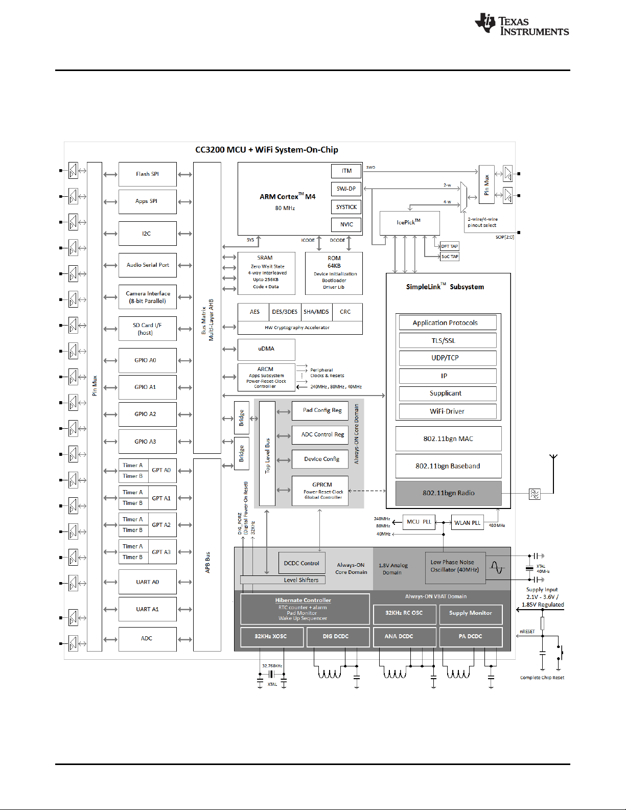
Architecture Overview
1.2 Architecture Overview
The building blocks of CC3200 system-on-chip are shown in Figure 1-1
Figure 1-1. CC3200 MCU and WIFI System-on-Chip
www.ti.com
24
Architecture Overview
Copyright © 2014–2018, Texas Instruments Incorporated
SWRU367D–June 2014–Revised May 2018
Submit Documentation Feedback
Page 25

www.ti.com
1.3 Functional Overview
The following sections provide an overview of the main components of the CC3200 system on chip (SoC)
from a microcontroller point of view.
1.3.1 Processor Core
1.3.1.1 ARM CortexTMM4 Processor Core
The CC3200 application MCU subsystem is built around an ARM Cortex-M4 processor core, which
provides outstanding computational performance and exceptional system response to interrupts at low
power consumption while optimizing memory footprint – making it an ideal fit for embedded applications.
Key features of ARM Cortex-M4 processor core are:
• Thumb-2 mixed 16- and 32-bit instruction set delivers the high performance expected of a 32-bit ARM
core in a compact memory size – enabling richer applications within a given device memory size.
• Single-cycle multiply instruction and hardware divide
• Atomic bit manipulation (bit-banding), delivering maximum memory use and streamlined peripheral
control
• Unaligned data access, enabling data to be efficiently packed into memory
• Fast code execution, permitting slower processor clock or increased sleep mode time.
• Hardware division and fast multiplier
• Deterministic, high-performance interrupt handling for time-critical applications
• Bit-band support for memory and select peripherals that includes atomic bit-band write and read
operations
• Configurable 4-pin JTAG and 2-pin (SWJ-DP) debug access
• Flash patch and breakpoint (FPB) unit to implement breakpoints and code patches
• Ultra-low power sleep modes
• Low active power consumption
• 80-MHz operation
Functional Overview
1.3.1.2 System Timer (SysTick)
The ARM Cortex-M4 processor core includes an integrated system timer, SysTick. SysTick provides a
simple, 24-bit, clear-on-write, decrementing, wrap-on-zero counter with a flexible control mechanism. The
counter is clocked on the system clock.
SysTick makes OS porting between Cortex-M4 devices much easier because there is no need to change
the OS system timer code. The SysTick timer integrates with the NVIC and can generate a SysTick
exception (exception type 15). In many OSes, a hardware timer generates interrupts so that the OS can
perform task management (for example, to allow multiple tasks to run at different time slots and to ensure
that no single task can lock up the entire system). To perform this function, the timer must be able to
generate interrupts and, if possible, be protected from user tasks so that user applications cannot change
the timer behavior.
The counter can be used in several different ways; for example:
• An RTOS tick timer that fires at a programmable rate (for example, 100 Hz) and invokes a SysTick
routine
• A high-speed alarm timer using the system clock
• A simple counter used to measure time to completion and time used
• An internal clock-source control based on missing or meeting durations
SWRU367D–June 2014–Revised May 2018
Submit Documentation Feedback
Copyright © 2014–2018, Texas Instruments Incorporated
Architecture Overview
25
Page 26

Functional Overview
1.3.1.3 Nested Vector Interrupt Controller (NVIC)
CC3200 includes the ARM NVIC. The NVIC and Cortex-M3 prioritize and handle all exceptions in handler
mode. The processor state is automatically stored to the stack on an exception and automatically restored
from the stack at the end of the interrupt service routine (ISR). The interrupt vector is fetched in parallel to
the state saving, thus enabling efficient interrupt entry. The processor supports tail-chaining, meaning that
back-to-back interrupts can be performed without the overhead of state saving and restoration. The NVIC
and Cortex-M4 processor prioritize and handle all exceptions in handler mode. The NVIC and the
processor core interface are closely coupled to enable low-latency interrupt processing and efficient
processing of late-arriving interrupts. The NVIC maintains knowledge of the stacked, or nested, interrupts
to enable tail-chaining of interrupts.
Key features are:
• Exceptional interrupt handling through hardware implementation of required register manipulations
• Deterministic, fast interrupt processing: always 12 cycles, or just 6 cycles with tail-chaining
• Programmable priority level for each interrupt
• Low-latency interrupt and exception handling
• Level and pulse detection of interrupt signals
• Grouping of interrupts into group priority and sub-priority interrupts
• Tail chaining of interrupts
1.3.1.4 System Control Block
The system control block (SCB) provides system implementation information and system control, including
configuration, control, and reporting of system exceptions.
www.ti.com
1.3.2 Memory
1.3.2.1 On-Chip SRAM
To enable low-cost applications, the CC3200 device family follows a flash-less approach. CC3200 has up
to 256KB of zero wait state, on-chip SRAM, to which application programs are downloaded and executed.
The SRAM is used for both code and data, and is connected to the Multi-Layer-AHB bus-matrix of the
chip. There is no restriction on relative size or partitioning of code and data.
The micro direct memory access (μDMA) controller can transfer data to and from SRAM and various
peripherals. The SRAM banks implement an advanced 4-way interleaved architecture which almost
eliminates the performance penalty when DMA and processor simultaneously access the SRAM.
Internal RAM has selective retention capability during low-power deep-sleep (LPDS) mode. Based on
need, during LPDS mode the application can choose to retain 256KB, 192KB, 128KB or 64KB. Retaining
the memory during low power mode provides a faster wakeup. TI provides an easy to use power
management framework for processor and peripheral context save and restore mechanism based on
SRAM retention. For more information, refer to the Power Management Framework User Guide in
Section 15.6.
1.3.2.2 ROM
CC3200 comes with factory programmed zero-wait-state ROM with the following firmware components:
• Device initialization
• Bootloader
• Peripheral driver library (DriverLib) release for product-specific peripherals and interfaces
When CC3200 powers up, or chip reset is released or returns from hibernate mode, the device
initialization procedure is executed first. After the chip hardware has been correctly configured, the
bootloader is executed, which loads the application code from non-volatile memory into on-chip SRAM
and makes a jump to the application code entry point.
26
Architecture Overview
Copyright © 2014–2018, Texas Instruments Incorporated
SWRU367D–June 2014–Revised May 2018
Submit Documentation Feedback
Page 27

www.ti.com
The CC3200 DriverLib is a software library that controls on-chip peripherals. The library performs both
peripheral initialization and control functions, with a choice of polled or interrupt-driven peripheral support.
The ROM DriverLib provides a rich set of drivers for peripheral and chip. It is aimed at reducing
application development time and improving solution robustness. TI recommends that applications make
extensive use of the DriverLib APIs to optimize memory and MIPS requirement of end applications.
1.3.3 Micro Direct Memory Access Controller (µDMA)
The CC3200 microcontroller includes a multichannel DMA controller, or μDMA. The μDMA controller
provides a way to offload data-transfer tasks from the Cortex-M4 processor, allowing more efficient use of
the processor and the available bus bandwidth. The μDMA controller can perform transfers between
memory and peripherals; it has dedicated channels for each supported on-chip module. The μDMA
controller can be programmed to automatically perform transfers between peripherals and memory as the
peripheral is ready to transfer more data.
The μDMA controller provides the following features:
• 32 configurable channels
• 80-MHz operation
• Support for memory to memory, memory to peripheral, and peripheral to memory in multiple transfer
modes
– Basic and simple transfer scenarios
– Ping-Pong for continuous data flow
– Scatter-gather for a programmable list of arbitrary transfers initiated from a single request
• Highly flexible and configurable channel operation
– Independently configured and operated channels
– Dedicated channels for supported on-chip modules
– One channel each for receive and transmit path for bidirectional modules
– Dedicated channel for software-initiated transfers
– Per-channel configurable bus arbitration scheme
– Software-initiated requests for any channel
• Two levels of priority
• Design optimizations for improved bus access performance between the µDMA controller and the
processor core
– µDMA controller access subordinate to core access
– Simultaneous concurrent access
• Data sizes of 8, 16, and 32 bits
• Transfer size is programmable in binary steps from 1 to 1024
• Source and destination address increment size of byte, half-word, word, or no increment
• Maskable peripheral requests
• Interrupt on transfer completion, with a separate interrupt per channel
Functional Overview
1.3.4 General Purpose Timer (GPT)
The CC3200 includes 4 instances of 32-bit user-programmable general purpose timers. GPTs count or
time external events that drive the timer input pins. Each GPT module (GPTM) block provides two 16-bit
timers or counters that can be configured to operate independently as timers or event counters, or
configured to operate as one 32-bit timer. The GPTM contains GPTM blocks with the following functional
options:
• Operating modes:
– 16- or 32-bit programmable one-shot timer
– 16- or 32-bit programmable periodic timer
SWRU367D–June 2014–Revised May 2018
Submit Documentation Feedback
Copyright © 2014–2018, Texas Instruments Incorporated
Architecture Overview
27
Page 28

Functional Overview
– 16-bit general-purpose timer with an 8-bit prescaler
– 16-bit input-edge count or time-capture modes
– 16-bit pulse-width modulation (PWM) mode with software-programmable output inversion of the
PWM signal
• Count up or down
• Ability to determine the elapsed time between the assertion of the timer interrupt and entry into the ISR
• Can trigger efficient transfers using the µDMA.
– Dedicated channel for each timer
– Burst request generated on timer interrupt
1.3.5 Watch Dog Timer (WDT)
The watchdog timer in the CC3200 restarts the system when it gets stuck due to an error and does not
respond as expected. The watchdog timer can be configured to generate an interrupt to the
microcontroller on its first time-out, and to generate a reset signal on its second time-out. Once the
watchdog timer is configured, the lock register can be written to prevent the timer configuration from being
inadvertently altered.
The watchdog timer provides the following features:
• 32-bit down-counter with a programmable load register
• Programmable interrupt generation logic with interrupt masking
• Lock register protection from runaway software
• Reset generation logic
www.ti.com
1.3.6 Multi-Channel Audio Serial Port (McASP)
CC3200 includes a configurable multichannel audio serial port for glue-less interfacing to audio CODEC
and DAC (speaker drivers). The audio port has two serializer / deserializers that can be individually
enabled to either transmit or receive and operate synchronously. Key features are:
• Two stereo I2S channels
– One stereo receive and one stereo transmit lines
– Two stereo transmit lines
• Programmable clock and frame-sync polarity (rising or falling edge)
• Programmable word length (bits per word): 16 and 24 bits
• Programmable fractional divider for bit-clock generation, up to 9 MHz.
1.3.7 Serial Peripheral Interface (SPI)
The serial peripheral interface (SPI) is a four-wire bidirectional communications interface that converts
data between parallel and serial. The SPI module performs serial-to-parallel conversion on data received
from a peripheral device, and parallel-to-serial conversion on data transmitted to a peripheral device. The
SPI allows a duplex serial communication between a local host and SPI-compliant external devices.
The CC3200 includes one SPI port dedicated to the application. Key features are
• Programmable interface operation for Freescale SPI, MICROWIRE, or TI synchronous serial interfaces
master and slave modes
• 3-pin and 4-pin mode
• Full duplex and half duplex
• Serial clock with programmable frequency, polarity, and phase
• Up to 20-MHz operation
• Programmable chip select polarity
• Programmable delay before the first SPI word is transmitted
• Programmable timing control between chip select and external clock generation
28
Architecture Overview
Copyright © 2014–2018, Texas Instruments Incorporated
SWRU367D–June 2014–Revised May 2018
Submit Documentation Feedback
Page 29

www.ti.com
• No dead cycle between two successive words in slave mode
• SPI word lengths of 8, 16, and 32 bits
• Efficient transfers using the μDMA controller
• Programmable interface operation for Freescale SPI, MICROWIRE, or TI-SSI
1.3.8 Inter-Integrated Circuit Interface (I2C)
The inter-integrated circuit (I2C) bus provides bidirectional data transfer through a two-wire design (a
serial data line SDA and a serial clock line SCL). The I2C bus interfaces to a wide variety of external I2C
devices such as sensors, serial memory, control ports of image sensors, and audio codecs. Multiple slave
devices can be connected to the same I2C bus. The CC3200 microcontroller includes one I2C module
with the following features:
• Master and slave modes of operation
• Master with arbitration and clock synchronization
• Multi-master support
• 7-bit addressing mode
• Standard (100 Kbps) and fast (400 Kbps) modes
1.3.9 Universal Asynchronous Receiver/Transmitter (UART)
A universal asynchronous receivers/transmitter (UART) is an integrated circuit used for RS-232 serial
communications. UARTs contain a transmitter (parallel-to-serial converter) and a receiver (serial-toparallel converter), each clocked separately.
The CC3200 device includes two fully programmable UARTs. The UART can generate individuallymasked interrupts from the RX, TX, modem status, and error conditions. The module generates a single
combined interrupt when any of the interrupts are asserted and unmasked.
The UARTs include the following features:
• Programmable baud-rate generator, allowing speeds up to 3 Mbps
• Separate 16 × 8 transmit (TX) and receive (RX) FIFOs to reduce CPU interrupt service loading
• Programmable FIFO length, including 1-byte deep operation providing conventional double-buffered
interface
• FIFO trigger levels of 1/8, 1/4, 1/2, 3/4, and 7/8
• Standard asynchronous communication bits for start, stop, and parity
• Line-break generation and detection
• Fully programmable serial interface characteristics:
– 5, 6, 7, or 8 data bits
– Even, odd, stick, or no-parity bit generation and detection
– 1 or 2 stop-bit generation
• RTS and CTS modem handshake support
• Standard FIFO-level and end-of-transmission interrupts
• Efficient transfers using µDMA
– Separate channels for transmit and receive
– Receive single request asserted when data is in the FIFO; burst request asserted at programmed
FIFO level
– Transmit single request asserted when there is space in the FIFO; burst request asserted at
programmed FIFO level
Functional Overview
SWRU367D–June 2014–Revised May 2018
Submit Documentation Feedback
Copyright © 2014–2018, Texas Instruments Incorporated
Architecture Overview
29
Page 30

Functional Overview
1.3.10 General Purpose Input / Output (GPIO)
All digital pins of the CC3200 device and some of the analog pins can be used as a general-purpose
input/output (GPIO). The GPIOs are grouped as 4 instance GPIO modules, each 8-bit. Supported features
include:
• Up to 24 GPIOs, depending on the functional pin configuration
• Interrupt capability for all GPIO pins
– Level or edge sensitive
– Rising or falling edge
– Selective interrupt masking
• Can trigger DMA operation
• Selectable wakeup source (one out of 6 pins)
• Programmable pad configuration
– Internal 5 µA pull-up and pull-down
– Configurable drive strength of 2, 4, 6, 8, 10, 12, and 14 mA
– Open-drain mode
• GPIO register readable through the high-speed internal bus matrix
1.3.11 Analog to Digital Converter (ADC)
The ADC peripheral converts a continuous analog voltage into a discrete digital number. The CC3200
device includes ADC modules with four input channels. Each ADC module features 12-bit conversion
resolution for the four input channels. Features include:
• Number of bits: 12-bit
• Effective nominal accuracy: 10 bits
• Four analog input channels
• Automatic round-robin sampling
• Fixed sampling interval of 16 µs per channel
• Automatic 16-bit time-stamping of every ADC samples based on the system clock
• Dedicated DMA channel to transfer ADC channel data to the application RAM.
www.ti.com
1.3.12 SD Card Host
The CC3200 includes an SD-Host interface for applications that require mass storage. The SD-Host
interface support is limited to 1-bit mode due to chip pin constraints.
1.3.13 Parallel Camera Interface
The CC3200 includes an 8-bit parallel camera port to enable image sensor-based applications.
1.3.14 Debug Interface
The CC3200 supports both IEEE Standard 1149.1 JTAG (4-wire) and the low-pin-count ARM SWD (2wire) debug interfaces. Depending on the board level configuration of the sense-on-power pull resistors,
by default the chip powers up with either the 4-wire JTAG or the 2-wire SWD interface.
As shown in Figure 1-1, the 4-wire JTAG signals from the chip pins are routed through an IcePick module.
TAPs other than the application MCU are reserved for TI production testing. A TAP select sequence must
be sent to the device to connect to the ARM Cortex M4 JTAG TAP. The 2-wire mode, however, directly
routes the ARM SWD-TMS and SWD-TCK pins directly to the respective chip pins.
30
Architecture Overview
Copyright © 2014–2018, Texas Instruments Incorporated
SWRU367D–June 2014–Revised May 2018
Submit Documentation Feedback
Page 31

www.ti.com
1.3.15 Hardware Cryptography Accelerator
The secure variant of the CC3200 includes a suite of high-throughput, state-of-the-art hardware
accelerators for fast computation of ciphers (AES, DES, 3-DES), hashing (SHA, MD5), and CRC
algorithms by the application. It is also referred as the data hashing and transform engine (DTHE). Further
details about the hardware cryptography accelerator will be addressed in the revision of this manual.
NOTE: Present production devices have the Crypto unlocked (Fuse Farm); a user application can
use these.
NOTE: Secure MCU ensures secure booting of the user application using the crypto engines. This
feature will be available in future revisions of the device.
1.3.16 Clock, Reset, and Power Management
The CC3200 system-on-chip includes the necessary clock and power management functionalities to build
a standalone battery-operated low power solution. Key features are:
• Primary clocks
– Slow clock: 32.768 KHz (+/-250 ppm)
• Used in RTC, Wi-Fi beacon listen timing in low power IDLE mode and some of the chip internal
sequencing
• On-chip, low power 32-KHz Xtal oscillator
• Support for externally-fed 32.768 KHz clock
• On-chip 32-KHz RC oscillator for initial wakeup
– Fast clock: 40 MHz (+/-20 ppm)
• Used in Wi-Fi radio and MCU.
• On-chip low phase-noise 40-MHz Xtal oscillator
• Support for externally-fed clean 40 MHz clock (such as TCXO)
• System and peripheral clocks are derived from internal PLL producing 240 MHz
• Flexible reset scheme
– The following resets are supported in CC3200
• External chip reset pin: the entire chip, including power management, is reset when the
nRESET pin is held low.
• Reset on hibernate: the entire core is reset when the chip goes through a hibernate cycle.
• Reset on watchdog: the application MCU is reset when the watchdog timer expires.
• Soft-reset: the application MCU is reset by software
– Complete system recovery from any stuck-at scenario can be achieved by using a combination of
WDT reset and hibernate sleep.
• On-chip power management
– The CC3200 supports two supply configurations:
• Wide voltage mode: 2.1 V to 3.6 V
• Powered by battery (2×1.5 V) or a regulated 3.3-V supply.
• Regulated 1.85 V
• For applications with on-board DCDC regulator
– A set of 3 on-chip high-efficiency DCDC converters produce the internal module supply voltages
when they are needed. These switching converters and their frequency plan are optimized to
minimize interference to WLAN radio.
• DIG-DCDC: Produces 0.9 V to 1.2 V for the core digital logic
• ANA1-DCDC: Produces low-ripple 1.8-V supply for the analog and RF. This is bypassed in the
Functional Overview
SWRU367D–June 2014–Revised May 2018
Submit Documentation Feedback
Copyright © 2014–2018, Texas Instruments Incorporated
Architecture Overview
31
Page 32

Functional Overview
regulated 1.85-V configuration.
• PA-DCDC: Produces regulated 1.8 V with extremely fast transient regulation for the WLAN RF
Transmit Power Amplifier. This is bypassed in the regulated 1.85-V configuration.
– A set of low dropout regulators (LDOs) are used in the radio subsystem to further regulate and filter
the ANA1-DCDC output before being fed to the analog circuits.
– On-chip factory-trimmed accurate band-gap voltage reference ensures the regulator outputs are
stable across process and temperature.
1.3.17 SimpleLink Subsystem
The SimpleLink subsystem provides fast, secured WLAN and Internet connections with 256-bit encryption.
The CC3200 device supports station, AP, and Wi-Fi Direct modes. The device also supports WPA2
personal and enterprise security and WPS 2.0. The Wi-Fi network processor includes an embedded IPv4
TCP/IP stack.
This multi-processor subsystem consists of the following:
• IPv4 network processor and Wi-Fi driver
• 802.11 b/g/n MAC
• 802.11 b/g/n PHY
• 802.11 b/g/n Radio
The SimpleLink subsystem is accessible from the application MCU over an asynchronous link, and can be
controlled through a complete set of SimpleLink host driver APIs provided as part of the ROM driver
library. The mode of usage is similar to that of an external MCU using the CC3100 device.
The co-location of the Wi-Fi subsystem on the same die imposes a few restrictions on the application
MCU. These will be covered in detail in Chapter 15.
www.ti.com
1.3.18 I/O Pads and Pin Multiplexing
The device makes extensive use of pin multiplexing to accommodate the large number of peripheral
functions in the smallest possible package. To achieve this configuration, pin multiplexing is controlled
using a combination of hardware configuration (at device reset) and register control.
The I/O pad and pin mux sections feature flexible wide-voltage I/Os. Supported features include:
• Programmable drive strength from 2 mA to 14 mA (nominal condition) in steps of 2 mA.
• Open drain mode
• Output buffer isolation
• Automatic output isolation during reset and hibernate
• Configurable pull-up and pull-down (10 µA nominal)
• Software-configurable pad state retention during LPDS
• All digital I/Os are nonfail-safe.
32
Architecture Overview
Copyright © 2014–2018, Texas Instruments Incorporated
SWRU367D–June 2014–Revised May 2018
Submit Documentation Feedback
Page 33

Chapter 2
SWRU367D–June 2014–Revised May 2018
Cortex-M4 Processor
Topic ........................................................................................................................... Page
2.1 Overview........................................................................................................... 34
2.2 Functional Description........................................................................................ 36
SWRU367D–June 2014–Revised May 2018
Submit Documentation Feedback
Copyright © 2014–2018, Texas Instruments Incorporated
Cortex-M4 Processor
33
Page 34

Overview
2.1 Overview
The CC3200 incorporates a dedicated instance of the ARM Cortex-M4 CPU core for executing application
code with or without RTOS. This processor core is not used in any manner for running any networking or
device management task.
This dedicated ARM Cortex-M4 core, along with large on-chip SRAM, a rich set of peripherals, and
advanced DC-DC-based power management, provides a robust, contention-free, high-performance
application platform at much lower power, lower cost, and smaller solution size when compared to
solutions based on discrete MCUs.
Features include:
• 32-bit ARM Cortex-M4 architecture optimized for small-footprint embedded applications
• 80-MHz operation
• Fast interrupt handling
• Thumb-2 mixed 16-/32-bit instruction set delivers the high performance expected of a 32-bit ARM core
in a compact memory size usually associated with 8- and 16-bit devices, typically in the range of a few
kilobytes of memory for microcontroller-class applications.
– Single-cycle multiply instruction and hardware divide
– Atomic bit manipulation (bit-banding), delivering maximum memory utilization and streamlined
peripheral control
– Unaligned data access, enabling data to be efficiently packed into memory
• 16-bit SIMD vector processing unit
• 3-stage pipeline Harvard architecture
• Hardware division and fast digital-signal-processing orientated multiply accumulate
• Saturating arithmetic for signal processing
• Deterministic, high-performance interrupt handling for time-critical applications
• Enhanced system debug with extensive breakpoints
• Serial-wire debug and serial-wire trace reduce the number of pins required for debugging and tracing
• Low-power consumption with multiple sleep modes
The ARM Cortex-M4 application processor core in the CC3200 does not include the floating point unit and
memory protection unit (FPU and MPU).
This chapter provides information on the implementation of the Cortex-M4 application processor in the
CC3200, including the programming model, the memory model, the exception model, fault handling, and
power management.
For technical details on the instruction set, see the Cortex-M4 instruction set chapter in the ARM®
Cortex™-M4 Devices Generic User Guide (ARM DUI 0553A).
www.ti.com
2.1.1 Block Diagram
The block diagram is shown in Figure 2-1.
34
Cortex-M4 Processor
Copyright © 2014–2018, Texas Instruments Incorporated
SWRU367D–June 2014–Revised May 2018
Submit Documentation Feedback
Page 35

www.ti.com
Overview
Figure 2-1. Application CPU Block Diagram
2.1.2 System-Level Interface
The Cortex-M4 application processor in the CC3200 provides multiple interfaces using AMBA™
technology to provide high-speed, low-latency memory accesses. The core supports unaligned data
accesses and implements atomic bit manipulation that enables faster peripheral controls, system
spinlocks, and thread-safe Boolean data handling.
2.1.3 Integrated Configurable Debug
The Cortex-M4 application processor implements an ARM CoreSight™-compliant serial wire JTAG-debug
port (SWJ-DP) interface. The SWJ-DP interface combines the SWD and JTAG debug ports into one
module. See the ARM Debug Interface V5 Architecture Specification for details on SWJ-DP.
The 4-bit trace interface from embedded trace macrocell (ETM) is not supported in the CC3200 due to pin
limitations. Instead, the processor integrates an instrumentation trace macrocell (ITM) alongside data
watchpoints and a profiling unit. A serial-wire viewer (SWV) can export a stream of software-generated
messages (printf style debug), data trace, and profiling information through a single pin to enable simple
and cost-effective profiling of the system trace events.
The flash patch and breakpoint unit (FPB) provides up to eight hardware breakpoint comparators for
debugging. The comparators in the FPB also provide remap functions for up to eight words of program
code in the code memory region. FPB also provides code patching capability; however, as the CC3200
application processor implements and executes from SRAM architecture, this type of patching is no longer
required.
For more information on the Cortex-M4 debug capabilities, see the ARM Debug Interface V5 Architecture
Specification.
SWRU367D–June 2014–Revised May 2018
Submit Documentation Feedback
Copyright © 2014–2018, Texas Instruments Incorporated
Cortex-M4 Processor
35
Page 36

Debug
ATB
Slave
Port
ARM® Trace
Bus (ATB)
Interface
Asynchronous FIFO
Trace Out
(serializer)
Serial Wire
Trace Port
(SWO)
APB
Sla
ve
Port
Advance
Peripheral
Bus (APB)
Interface
Overview
2.1.4 Trace Port Interface Unit (TPIU)
The TPIU acts as a bridge between the Cortex-M4 trace data from the ITM, and an off-chip trace port
analyzer, as shown in Figure 2-2.
Figure 2-2. TPIU Block Diagram
2.1.5 Cortex-M4 System Component Details
The Cortex-M4 application processor core includes the following system components:
• SysTck
A 24-bit count-down timer used as a real-time operating system (RTOS) tick timer or as a simple
counter (see Section 3.2.1).
• Nested Vectored Interrupt Controller (NVIC)
An embedded interrupt controller that supports low-latency interrupt processing (see Nested Vectored
Interrupt Controller (NVIC) in Section 3.2.2).
• System Control Block (SCB)
The programming model interface to the processor. The SCB provides system implementation
information and system control, including configuration, control, and reporting of system exceptions
(see System Control Block (SCB) in Section 3.2.3).
www.ti.com
2.2 Functional Description
2.2.1 Programming Model
This section describes the Cortex-M4 programming model and includes the individual core register
descriptions, information about the processor modes, and privilege levels for software execution and
stacks.
2.2.1.1 Processor Mode and Privilege Levels for Software Execution
The Cortex-M4 has two modes of operation:
• Thread mode, to execute application software. The processor enters thread mode when it comes out
of reset.
• Handler mode, to handle exceptions. When the processor has finished exception processing, it returns
36
to thread mode.
In addition, the Cortex-M4 has two privilege levels:
• Underprivileged
In this mode, the software has the following restrictions:
– Limited access to the MSR and MRS instructions, and no use of the CPS instruction
– No access to the system timer, NVIC, or system control block
Cortex-M4 Processor
Copyright © 2014–2018, Texas Instruments Incorporated
SWRU367D–June 2014–Revised May 2018
Submit Documentation Feedback
Page 37

www.ti.com
– Possibly restricted access to memory or peripherals
• Privileged
In this mode, the software can use all instructions and has access to all resources
In thread mode, the CONTROL register controls whether software execution is privileged or unprivileged.
In handler mode, software execution is always privileged.
Only privileged software can write to the CONTROL register to change the privilege level for software
execution in thread mode. Unprivileged software can use the SVC instruction to make a supervisor call to
transfer control to privileged software.
2.2.1.2 Stacks
The processor uses a full descending stack, meaning that the stack pointer indicates the last stacked item
on the memory. When the processor pushes a new item onto the stack, it decrements the stack pointer,
then writes the item to the new memory location. The processor implements two stacks: the main stack
and the process stack, with a pointer for each held in independent registers (see the SP register).
In thread mode, the CONTROL register controls whether the processor uses the main stack or the
process stack. In handler mode, the processor always uses the main stack. The options for processor
operations are shown in Table 2-1.
Processor Mode Use Privilege Level Stack Used
Thread Applications
Handler Exception handlers Always privileged Main stack
(1)
See CONTROL register in Section 2.2.2.1.2.8.
Functional Description
Table 2-1. Summary of Processor Mode, Privilege Level, and Stack Use
Privileged or unprivileged
(1)
(1)
Main stack or process stack
2.2.2 Register Description
2.2.2.1 Registers
2.2.2.1.1 Register Map
Figure 2-2 shows the Cortex-M4 register set. Table 2-2 lists the core registers. The core registers are not
memory-mapped and are accessed by register name, so the base address is n/a (not applicable) and
there is no offset.
SWRU367D–June 2014–Revised May 2018
Submit Documentation Feedback
Copyright © 2014–2018, Texas Instruments Incorporated
Cortex-M4 Processor
37
Page 38

Functional Description
www.ti.com
Figure 2-3. Cortex-M4 Register Set
Table 2-2. Processor Register Map
Offset Name Type Reset Description
- R0 R/W - Cortex General-Purpose Register 0
- R1 R/W - Cortex General-Purpose Register 1
- R2 R/W - Cortex General-Purpose Register 2
- R3 R/W - Cortex General-Purpose Register 3
- R4 R/W - Cortex General-Purpose Register 4
- R5 R/W - Cortex General-Purpose Register 5
- R6 R/W - Cortex General-Purpose Register 6
- R7 R/W - Cortex General-Purpose Register 7
- R8 R/W - Cortex General-Purpose Register 8
- R9 R/W - Cortex General-Purpose Register 9
- R10 R/W - Cortex General-Purpose Register 10
- R11 R/W - Cortex General-Purpose Register 11
- R12 R/W - Cortex General-Purpose Register 12
- SP R/W - Stack Pointer
- LR R/W 0xFFFF.FFFF Link Register
- PC R/W - Program Counter
- PSR R/W 0x0100.0000 Program Status Register
- PRIMASK R/W 0x0000.0000 Priority Mask Register
- FAULTMASK R/W 0x0000.0000 Fault Mask Register
- BASEPRI R/W 0x0000.0000 Base Priority Mask Register
- CONTROL R/W 0x0000.0000 Control Register
38
Cortex-M4 Processor
SWRU367D–June 2014–Revised May 2018
Submit Documentation Feedback
Copyright © 2014–2018, Texas Instruments Incorporated
Page 39

www.ti.com
Offset Name Type Reset Description
- FPSC R/W - Floating-Point Status Control (N/A for
2.2.2.1.2 Register Descriptions
This section lists and describes the Cortex-M4 registers. The core registers are not memory-mapped, and
are accessed by register name rather than offset.
NOTE: The register type shown in the register descriptions refers to type during program execution
in thread mode and handler mode. Debug access may differ.
The Rn registers are 32-bit general-purpose registers for data operations, and can be accessed from
either privileged or unprivileged mode.
2.2.2.1.2.1 Stack Pointer (SP)
In thread mode, the function of this register changes depending on the ASP bit in the Control Register
(CONTROL) register. When the ASP bit is clear, this register is the main stack pointer (MSP). When the
ASP bit is set, this register is the process stack pointer (PSP). On reset, the ASP bit is clear, and the
processor loads the MSP with the value from address 0x0000 0000. The MSP can only be accessed in
privileged mode; the PSP can be accessed in either privileged or unprivileged mode.
Functional Description
Table 2-2. Processor Register Map (continued)
CC3200)
2.2.2.1.2.2 Link Register (LR)
The Link register (LR) stores the return information for subroutines, function calls, and exceptions. The
Link register can be accessed from either privileged or unprivileged mode.
EXC_RETURN is loaded into the LR on exception entry.
2.2.2.1.2.3 Program Counter (PC)
The program counter (PC) contains the current program address. On reset, the processor loads the PC
with the value of the reset vector, which is at address 0x0000 0004. Bit 0 of the reset vector is loaded into
the THUMB bit of the EPSR at reset and must be 1. The PC register can be accessed in either privileged
or unprivileged mode.
2.2.2.1.2.4 Program Status Register (PSR)
NOTE: This register is also referred to as xPSR.
The Program Status (PSR) register has three functions, and the register bits are assigned to the different
functions:
• Application Program Status (APSR) register, bits 31:27, bits 19:16
• Execution Program Status (EPSR) register, bits 26:24, 15:10
• Interrupt Program Status (IPSR) register, bits 7:0
The PSR, IPSR, and EPSR registers can only be accessed in privileged mode; the APSR register can be
accessed in either privileged or unprivileged mode.
APSR contains the current state of the condition flags from previous instruction executions. EPSR
contains the Thumb state bit and the execution state bits for the if-then (IT) instruction or the interruptiblecontinuable instruction (ICI) field for an interrupted load multiple or store multiple instruction. Attempts to
read the EPSR directly through application software using the MSR instruction always return zero.
Attempts to write the EPSR using the MSR instruction in application software are always ignored. Fault
handlers can examine the EPSR value in the stacked PSR to determine the operation that faulted.
SWRU367D–June 2014–Revised May 2018
Submit Documentation Feedback
Copyright © 2014–2018, Texas Instruments Incorporated
Cortex-M4 Processor
39
Page 40

Functional Description
IPSR contains the exception type number of the current interrupt service routine (ISR).
These registers can be accessed individually, or as a combination of any two or all three registers, using
the register name as an argument to the MSR or MRS instructions. For example, all of the registers can
be read using PSR with the MRS instruction, or APSR only can be written to using APSR with the MSR
instruction. Table 2-3 shows the possible register combinations for the PSR. See the MRS and MSR
instruction descriptions in the Cortex-M4 instruction set chapter in the ARM Cortex-M4 Devices Generic
User Guide (ARM DUI 0553A) for more information about how to access the program status registers.
Table 2-3. PSR Register Combinations
Register Type Combination
PSR PSR R/W
IEPSR RO EPSR and IPSR
IAPSR R/W
EAPSR R/W
(1)
The processor ignores writes to the IPSR bits.
(2)
Reads of the EPSR bits return zero, and the processor ignores writes to these bits
2.2.2.1.2.5 Priority Mask Register (PRIMASK)
The PRIMASK register prevents activation of all exceptions with programmable priority. Reset, nonmaskable interrupt (NMI), and hard fault are the only exceptions with fixed priority. Exceptions should be
disabled when they might impact the timing of critical tasks. This register is only accessible in privileged
mode. The MSR and MRS instructions are used to access the PRIMASK register, and the CPS instruction
may be used to change the value of the PRIMASK register. See the Cortex-M4 instruction set chapter in
the ARM Cortex-M4 Devices Generic User Guide (ARM DUI 0553A) for more information on these
instructions.
(1)
(2)
(1) (2)
www.ti.com
APSR, EPSR, and IPSR
APSR and IPSR
APSR and EPSR
2.2.2.1.2.6 Fault Mask Register (FAULTMASK)
The FAULTMASK register prevents activation of all exceptions except for the Non-Maskable Interrupt
(NMI). Exceptions should be disabled when they might impact the timing of critical tasks. This register is
only accessible in privileged mode. The MSR and MRS instructions are used to access the FAULTMASK
register, and the CPS instruction may be used to change the value of the FAULTMASK register. See the
Cortex™-M4 instruction set chapter in the ARM® Cortex™-M4 Devices Generic User Guide (ARM DUI
0553A) for more information on these instructions.
2.2.2.1.2.7 Base Priority Mask Register (BASEPRI)
The BASEPRI register defines the minimum priority for exception processing. When BASEPRI is set to a
nonzero value, it prevents the activation of all exceptions with the same or lower priority level as the
BASEPRI value. Exceptions should be disabled when they might impact the timing of critical tasks. This
register is only accessible in privileged mode.
2.2.2.1.2.8 Control Register (CONTROL)
The CONTROL register controls the stack used and the privilege level for software execution when the
processor is in thread mode, and indicates whether the FPU state is active. This register is only accessible
in privileged mode.
Handler mode always uses the MSP, so the processor ignores explicit writes to the ASP bit of the
CONTROL register when in handler mode. The exception entry and return mechanisms automatically
update the CONTROL register based on the EXC_RETURN value. In an OS environment, threads running
in thread mode should use the process stack, and the kernel and exception handlers should use the main
stack. By default, thread mode uses the MSP. To switch the stack pointer used in thread mode to the
PSP, either use the MSR instruction to set the ASP bit, as detailed in the Cortex-M4 instruction set
chapter in the ARM Cortex-M4 Devices Generic User Guide (ARM DUI 0553A), or perform an exception
return to thread mode with the appropriate EXC_RETURN value.
40
Cortex-M4 Processor
Copyright © 2014–2018, Texas Instruments Incorporated
SWRU367D–June 2014–Revised May 2018
Submit Documentation Feedback
Page 41

www.ti.com
NOTE: When changing the stack pointer, software must use an ISB instruction immediately after
the MSR instruction, ensuring that instructions after the ISB execute use the new stack
pointer. See the Cortex-M4 instruction set chapter in the ARM Cortex-M4 Devices Generic
User Guide (ARM DUI 0553A).
2.2.2.1.3 Exceptions and Interrupts
The Cortex-M4 application processor in the CC3200 supports interrupts and system exceptions. The
processor and the nested vectored interrupt controller (NVIC) prioritize and handle all exceptions. An
exception changes the normal flow of software control. The processor uses handler mode to handle all
exceptions except for reset. See Section 2.2.4.7 for more information.
The NVIC registers control interrupt handling. See nested vectored interrupt controller (NVIC) for more
information.
2.2.2.1.4 Data Types
The Cortex-M4 supports 32-bit words, 16-bit halfwords, and 8-bit bytes. The processor also supports 64bit data transfer instructions. All instruction and data memory accesses are little endian.
2.2.3 Memory Model
This section describes the processor memory map, the behavior of memory accesses, and the bit-banding
features. The processor has a fixed memory map that provides up to 4 GB of addressable memory.
The memory map of the CC3200 microcontroller subsystem is provided in Table 2-4. In this manual,
register addresses are given as a hexadecimal increment, relative to the base address of the module, as
shown in the memory map.
The regions for SRAM and peripherals include bit-band regions. Bit-banding provides atomic operations to
bit data (see Section 2.2.3.1).
The processor reserves regions of the private peripheral bus (PPB) address range for core peripheral
registers (see the Cortex-M4 Peripherals, Chapter 3).
Functional Description
NOTE: Within the memory map, attempts to read or write addresses in reserved spaces result in a
bus fault. In addition, attempts to write addresses in the flash range also result in a bus fault.
Table 2-4. Memory Map
Start Address End Address Description Comment
0x0000.0000 0x0007.FFFF On-chip ROM (Bootloader + DriverLib)
0x2000.0000 0x2003.FFFF Bit-banded on-chip SRAM
0x2200.0000 0x23FF.FFFF
0x4000.0000 0x4000.0FFF Watchdog timer A0
0x4000.4000 0x4000.4FFF GPIO port A0
0x4000.5000 0x4000.5FFF GPIO port A1
0x4000.6000 0x4000.6FFF GPIO port A2
0x4000.7000 0x4000.7FFF GPIO port A3
0x4000.C000 0x4000.CFFF UART A0
0x4000.D000 0x4000.DFFF UART A1
0x4002.0000 0x4002.07FF I2C A0 (Master)
0x4002.0800 0x4002.0FFF I2C A0 (Slave)
0x04003.0000 0x4003.0FFF General-purpose timer A0
0x04003.1000 0x4003.1FFF General-purpose timer A1
0x04003.2000 0x4003.2FFF General-purpose timer A2
Bit-band alias of 0x2000.0000 through
0x200F.FFFF
SWRU367D–June 2014–Revised May 2018
Submit Documentation Feedback
Copyright © 2014–2018, Texas Instruments Incorporated
Cortex-M4 Processor
41
Page 42

Functional Description
Start Address End Address Description Comment
0x04003.3000 0x4003.3FFF General-purpose timer A3
0x400F.7000 0x400F.7FFF Configuration registers
0x400F.E000 0x400F.EFFF System control
0x400F.F000 0x400F.FFFF µDMA
0x4200.0000 0x43FF.FFFF
0x4401.C000 0x4401.EFFF McASP
0x4402.0000 0x4402.0FFF FlashSPI
0x4402.1000 0x4402.2FFF GSPI
0x4402.5000 0x4402.5FFF MCU reset clock manager
0x4402.6000 0x4402.6FFF MCU configuration space
0xE000.0000 0xE000.0FFF Instrumentation trace Macrocell
0xE000.1000 0xE000.1FFF Data watchpoint and trace (DWT)
0xE000.2000 0xE000.2FFF Flash patch and breakpoint (FPB)
0xE000.E000 0xE000.EFFF Cortex-M4 Peripherals (NVIC, SysTick,SCB)
0xE004.0000 0xE004.0FFF Trace port interface unit (TPIU)
0xE004.1000 0xE004.1FFF Reserved for embedded trace macrocell (ETM)
www.ti.com
Table 2-4. Memory Map (continued)
Bit band alias of 0x4000.0000 through
0x400F.FFFF
Used for external serial
flash
Used by application
processor
TM
2.2.3.1 Bit-Banding
A bit-band region maps each word in a bit-band alias region to a single bit in the bit-band region. In ARM
Cortex-M4 architecture, the bit-band regions occupy the lowest 1 MB of the SRAM. Accesses to the 32MB SRAM alias region map to the 1-MB SRAM bit-band region, as shown in Table 2-5.
NOTE: A word access to the SRAM or the peripheral bit-band alias region maps to a single bit in the
SRAM or peripheral bit-band region.
A word access to a bit-band address results in a word access to the underlying memory, and
similarly for halfword and byte accesses. This allows bit-band accesses to match the access
requirements of the underlying peripheral.
The CC3200 family of Wi-Fi microcontrollers support up to 256 Kbyte of on-chip SRAM for code and data.
The SRAM starts from address 0x2000 0000.
Start End Memory Region Instruction and Data
0x2000.0000 0x2003.FFFF SRAM bit-band region Direct accesses to this memory
0x2200.0000 0x23FF.FFFF SRAM bit-band alias Data accesses to this region
Table 2-5. SRAM Memory Bit-Banding Regions
Address Range
Accesses
range behave as SRAM
memory accesses, but this
region is also bit addressable
through bit-band alias.
are remapped to bit band
region. A write operation is
performed as read-modifywrite. Instruction accesses are
not remapped.
42
Bit-banding for peripherals is not supported in the CC3200.
Cortex-M4 Processor
Copyright © 2014–2018, Texas Instruments Incorporated
SWRU367D–June 2014–Revised May 2018
Submit Documentation Feedback
Page 43

7 0
B0
B1
B2
B3
31 24 23 16 15 8 7 0
B3 B2 B1 B0
Memory Register
Address A
A+1
l
sbyte
A+2
A+3
msbyte
www.ti.com
2.2.3.1.1 Directly Accessing an Alias Region
Writing to a word in the alias region updates a single bit in the bit-band region.
Bit 0 of the value written to a word in the alias region determines the value written to the targeted bit in the
bit-band region. Writing a value with bit 0 set writes a 1 to the bit-band bit, and writing a value with bit 0
clear writes a 0 to the bit-band bit.
Bits 31:1 of the alias word have no effect on the bit-band bit. Writing 0x01 has the same effect as writing
0xFF. Writing 0x00 has the same effect as writing 0x0E.
When reading a word in the alias region, 0x0000 0000 indicates that the targeted bit in the bit-band region
is clear and 0x0000 0001 indicates that the targeted bit in the bit-band region is set.
2.2.3.1.2 Directly Accessing a Bit-Band Region
Behavior of memory accesses describes the behavior of direct byte, halfword, or word accesses to the bitband regions.
2.2.3.2 Data Storage
The processor views memory as a linear collection of bytes numbered in ascending order from zero. For
example, bytes 0-3 hold the first stored word, and bytes 4-7 hold the second stored word. Data is stored in
little-endian format, with the least-significant byte (lsbyte) of a word stored at the lowest-numbered byte,
and the most-significant byte (msbyte) stored at the highest-numbered byte. Figure 2-4 illustrates how
data is stored.
Functional Description
2.2.3.3 Synchronization Primitives
The Cortex-M4 instruction set includes pairs of synchronization primitives which provide a non-blocking
mechanism that a thread or process can use to obtain exclusive access to a memory location. Software
can use these primitives to perform a guaranteed read-modify-write memory update sequence or for a
semaphore mechanism.
A pair of synchronization primitives consists of:
• A load-exclusive instruction, to read the value of a memory location and request exclusive access to
that location.
• A store-exclusive instruction, to attempt to write to the same memory location and return a status bit to
a register. If this status bit is clear, it indicates that the thread or process gained exclusive access to
the memory and the write succeeds; if this status bit is set, it indicates that the thread or process did
not gain exclusive access to the memory and no write was performed.
The pairs of load-exclusive and store-exclusive instructions are:
• The word instructions LDREX and STREX
• The halfword instructions LDREXH and STREXH
• The byte instructions LDREXB and STREXB
SWRU367D–June 2014–Revised May 2018
Submit Documentation Feedback
Figure 2-4. Data Storage
Copyright © 2014–2018, Texas Instruments Incorporated
Cortex-M4 Processor
43
Page 44

Functional Description
Software must use a load-exclusive instruction with the corresponding store-exclusive instruction. To
perform an exclusive read-modify-write of a memory location, software must:
1. Use a load-exclusive instruction to read the value of the location.
2. Modify the value, as required.
3. Use a store-exclusive instruction to attempt to write the new value back to the memory location.
4. Test the returned status bit. If the status bit is clear, the read-modify-write completed successfully. If
the status bit is set, no write was performed, which indicates that the value returned at Step 1 might be
out of date. The software must retry the entire read-modify-write sequence.
Software can use the synchronization primitives to implement a semaphore as follows:
1. Use a load-exclusive instruction to read from the semaphore address, to check whether the semaphore
is free.
2. If the semaphore is free, use a store-exclusive to write the claim value to the semaphore address.
3. If the returned status bit from Step 2 indicates that the store-exclusive succeeded, then the software
has claimed the semaphore. However, if the store-exclusive failed, another process might have
claimed the semaphore after the software performed Step 1.
The Cortex-M4 includes an exclusive access monitor that tags the fact that the processor has executed a
load-exclusive instruction. The processor removes its exclusive access tag if:
• It executes a CLREX instruction.
• It executes a store-exclusive instruction, regardless of whether the write succeeds.
• An exception occurs, which means the processor can resolve semaphore conflicts between different
threads.
For more information about the synchronization primitive instructions, see the Cortex-M4 instruction set
chapter in the ARM Cortex-M4 Devices Generic User Guide (ARM DUI 0553A).
www.ti.com
2.2.4 Exception Model
The ARM Cortex-M4 application processor in the CC3200 and the nested vectored interrupt controller
(NVIC) prioritize and handle all exceptions in handler mode. The processor state is automatically stored to
the stack on an exception, and automatically restored from the stack at the end of the interrupt service
routine (ISR). The vector is fetched in parallel to the state saving, enabling efficient interrupt entry. The
processor supports tail-chaining, which enables back-to-back interrupts to be performed without the
overhead of state saving and restoration.
Table 2-6 lists all exception types. Software can set eight priority levels on seven of these exceptions
(system handlers) as well as on 70 interrupts (listed in Table 2-6). Priorities on the system handlers are
set with the NVIC System Handler Priority n (SYSPRIn) registers. Interrupts are enabled through the NVIC
Interrupt Set Enable n (ENn) register and prioritized with the NVIC Interrupt Priority n (PRIn) registers.
Priorities can be grouped by splitting priority levels into preemption priorities and subpriorities. All the
interrupt registers are described in Section 3.2.2.
Internally, the highest user-programmable priority (0) is treated as fourth priority, after a reset, nonmaskable interrupt (NMI), and a hard fault, in that order. Note that 0 is the default priority for all the
programmable priorities.
NOTE: After a write to clear an interrupt source, it may take several processor cycles for the NVIC to
see the interrupt source de-assert. Thus, if the interrupt clear is done as the last action in an
interrupt handler, it is possible for the interrupt handler to complete while the NVIC sees the
interrupt as still asserted, causing the interrupt handler to be re-entered errantly. This
situation can be avoided by either clearing the interrupt source at the beginning of the
interrupt handler or by performing a read or write after the write to clear the interrupt source
(and flush the write buffer).
44
See nested vectored interrupt controller (NVIC) for more information on exceptions and interrupts.
Cortex-M4 Processor
Copyright © 2014–2018, Texas Instruments Incorporated
SWRU367D–June 2014–Revised May 2018
Submit Documentation Feedback
Page 45

www.ti.com
2.2.4.1 Exception States
Each exception is in one of the following states:
• Inactive: The exception is not active and not pending.
• Pending: The exception is waiting to be serviced by the processor. An interrupt request from a
peripheral or from software can change the state of the corresponding interrupt to pending.
• Active: An exception being serviced by the processor but has not completed. An exception handler can
interrupt the execution of another exception handler. In this case, both exceptions are in the active
state.
• Active and Pending: The exception is being serviced by the processor, and there is a pending
exception from the same source.
2.2.4.2 Exception Types
The exception types are:
• Reset: Reset is invoked on power up or a warm reset. The exception model treats reset as a special
form of exception. When reset is asserted, the operation of the processor stops, potentially at any point
in an instruction. When reset is deasserted, execution restarts from the address provided by the reset
entry in the vector table. Execution restarts as privileged execution in thread mode.
• NMI: A non-maskable interrupt (NMI) can be signaled using the NMI signal, or triggered by software
using the Interrupt Control and State (INTCTRL) register. This exception has the highest priority other
than reset. NMI is permanently enabled and has a fixed priority of –2. NMIs cannot be masked or
prevented from activation by any other exception or preempted by any exception other than reset. NMI
in the CC3200 is reserved for the internal system, and is not available for application usage.
• Hard Fault: A hard fault is an exception that occurs because of an error during exception processing,
or because an exception cannot be managed by any other exception mechanism. Hard faults have a
fixed priority of –1, meaning they have higher priority than any exception with configurable priority.
• Memory Management Fault: A memory management fault is an exception that occurs because of a
memory-protection-related fault, including access violation and no match. The MPU or the fixedmemory protection constraints determine this fault, for both instruction and data memory transactions.
This fault is used to abort instruction accesses to Execute Never (XN) memory regions, even if the
MPU is disabled.
• Bus Fault: A bus fault is an exception that occurs because of a memory-related fault for an instruction
or data memory transaction such as a prefetch fault or a memory access fault. This fault can be
enabled or disabled.
• Usage Fault: A usage fault is an exception that occurs because of a fault related to instruction
execution, such as:
– An undefined instruction
– An illegal unaligned access
– Invalid state on instruction execution
– An error on exception return. An unaligned address on a word or halfword memory access or
division by zero can cause a usage fault when the core is properly configured.
• SVCall: A supervisor call (SVC) is an exception that is triggered by the SVC instruction. In an OS
environment, applications can use SVC instructions to access OS kernel functions and device drivers.
• Debug Monitor: This exception is caused by the debug monitor (when not halting). This exception is
only active when enabled. This exception does not activate if it is a lower priority than the current
activation.
• PendSV: PendSV is a pendable, interrupt-driven request for system-level service. In an OS
environment, use PendSV for context switching when no other exception is active. PendSV is triggered
using the Interrupt Control and State (INTCTRL) register.
• SysTick: A SysTick exception is an exception that the system timer generates when it reaches zero
when enabled to generate an interrupt. Software can also generate a SysTick exception using the
Interrupt Control and State (INTCTRL) register. In an OS environment, the processor can use this
exception as system tick.
Functional Description
SWRU367D–June 2014–Revised May 2018
Submit Documentation Feedback
Copyright © 2014–2018, Texas Instruments Incorporated
Cortex-M4 Processor
45
Page 46

Functional Description
• Interrupt (IRQ): An interrupt, or IRQ, is an exception signaled by a peripheral or generated by a
software request and fed through the NVIC (prioritized). All interrupts are asynchronous to instruction
execution. In the system, peripherals use interrupts to communicate with the processor. Table 2-5 lists
the interrupts on the CC3200 application processor
For an asynchronous exception, other than reset, the processor can execute another instruction between
when the exception is triggered and when the processor enters the exception handler.
Privileged software can disable the exceptions that Table 2-6 show as having configurable priority (see the
SYSHNDCTRL register and the DIS0 register).
For more information about hard faults, memory management faults, bus faults, and usage faults, see
Section 2.2.5.
Exception Type Vector Number Priority
- 0 - 0x0000.0000 Stack top is loaded from
Reset 1 -3 (highest) 0x0000.0004 Asynchronous
Non-Maskable Interrupt
(NMI)
Hard Fault 3 -1 0x0000.000C Memory Management 4 programmable
Bus Fault 5 programmable
Usage Fault 6 programmable
- 10-Jul - - Reserved
SVCall 11 programmable
Debug Monitor 12 programmable
- 13 - - Reserved
PendSV 14 programmable
SysTick 15 programmable
Interrupts 16 and above programmable
(1)
a. 0 is the default priority for all the programmable priorities.
(2)
b. See Figure 2-5.
(3)
See SYSPRI1 on Table 3-3.
(4)
d. See PRIn registers.
Table 2-6. Exception Types
(1)
2 -2 0x0000.0008 Asynchronous
(3)
(3)
(3)
(3)
(3)
(3)
(3)
(4)
Vector Address or
Offset
(2)
Activation
the first entry of the
vector table on reset.
0x0000.0010 Synchronous
0x0000.0014 Synchronous when
precise and
asynchronous when
imprecise
0x0000.0018 Synchronous
0x0000.002C Synchronous
0x0000.0030 Synchronous
0x0000.0038 Asynchronous
0x0000.003C Asynchronous
0x0000.0040 and above Asynchronous
www.ti.com
Interrupt Number
(Bit in Interrupt
46
Cortex-M4 Processor
Table 2-7. CC3200 Application Processor Interrupts
Vector Adderess or Offset Description Type
Registers)
0 0x0000.0040 GPIO Port 0 (GPIO 0-7)
1 0x0000.0044 GPIO Port A1 (GPIO 8-15)
2 0x0000.0048 GPIO Port A2 (GPIO 16-23)
3 0x0000.004C GPIO Port A3 (GPIO 24-31)
5 0x0000.0054 UART0
6 0x0000.0058 UART1
8 0x0000.0060 I2C
14 0x0000.0078 ADC Channel-0
15 0x0000.007C ADC Channel-1
16 0x0000.0080 ADC Channel-2
SWRU367D–June 2014–Revised May 2018
Submit Documentation Feedback
Copyright © 2014–2018, Texas Instruments Incorporated
Page 47

www.ti.com
Table 2-7. CC3200 Application Processor Interrupts (continued)
Interrupt Number
(Bit in Interrupt
Registers)
17 0x0000.0084 ADC Channel-3
18 0x0000.0088 WDT
19 0x0000.008C 16/32-Bit Timer A0A
20 0x0000.0090 16/32-Bit Timer A0B
21 0x0000.0094 16/32-Bit Timer A1A
22 0x0000.0098 16/32-Bit Timer A1B
23 0x0000.009C 16/32-Bit Timer A2A
24 0x0000.00A0 16/32-Bit Timer A2B
35 0x0000.00CC 16/32-Bit Timer A3A
36 0x0000.00D0 16/32-Bit Timer A3B
46 0x0000.00F8 uDMA Software Intr
47 0x0000.00FC uDMA Error Intr
161 0x0000.02C4 I2S
163 0x0000.02CC Camera
168 0x0000.02E0 RAM WR Error
171 0x0000.02EC Network Intr
175 0x0000.02FC Shared SPI interrupt (for SFLASH)
176 0x0000.0300 SPI
177 0x0000.0304 Link SPI (APPS to NWP)
Vector Adderess or Offset Description Type
Functional Description
2.2.4.3 Exception Handlers
The processor handles exceptions using:
• Interrupt service routines (ISRs): Interrupts (IRQx) are the exceptions handled by ISRs.
• Fault handlers: Hard fault, memory-management fault, usage fault, and bus fault are fault exceptions
handled by the fault handlers.
• System handlers: NMI, PendSV, SVCall, SysTick, and the fault exceptions are all system exceptions
handled by system handlers.
2.2.4.4 Vector Table
The vector table contains the reset value of the stack pointer and the start addresses, also called
exception vectors, for all exception handlers. The vector table is constructed using the vector address or
offset shown in Table 2-6. Figure 2-5 shows the order of the exception vectors in the vector table. The
least-significant bit of each vector must be 1, indicating that the exception handler is thumb code.
SWRU367D–June 2014–Revised May 2018
Submit Documentation Feedback
Copyright © 2014–2018, Texas Instruments Incorporated
Cortex-M4 Processor
47
Page 48

Exception number
(N+16)
.
.
.
18
17
16
15
14
13
12
11
10
9
8
7
6
5
4
3
2
1
0
I
RQ number
(N)
2
1
0
-1
-2
-5
-10
-11
-12
-13
-14
Offset
0x040
+ 0x(N*4)
.
.
.
0x004C
0x0048
0x0044
0x0040
0x003C
0x0038
0x002C
0x0018
0x0014
0x0010
0x000C
0x0008
0x0004
0x0000
Vector
IRQ N
.
.
.
IRQ2
IRQ1
IRQ0
Systick
PendSV
Reserve
d
Reserved for Debug
SVCall
Reserved
Usage
fault Bus
fault
Memory management
fault Hard fault
NMI
Reset
Initial SP value
Functional Description
www.ti.com
Figure 2-5. Vector Table
2.2.4.5 Exception Priorities
48
On system reset, the vector table is fixed at address 0x0000 0000. Privileged software can write to the
Vector Table Offset (VTABLE) register to relocate the vector table start address to a different memory
location, in the range 0x0000 0400 to 0x3FFF FC00. When configuring the VTABLE register, the offset
must be aligned on a 1024-byte boundary.
As shown in Table 2-6, all exceptions have an associated priority, with a lower priority value indicating a
higher priority and configurable priorities for all exceptions except reset, hard fault, and NMI. If software
does not configure any priorities, then all exceptions with a configurable priority have a priority of 0.
NOTE: Configurable priority values for the CC3200 implementation are in the range 0-7. This means
that the reset, hard fault, and NMI exceptions (NMI is reserved for use by the system) with
fixed negative priority values always have higher priority than any other exception.
For example, assigning a higher priority value to IRQ[0] and a lower priority value to IRQ[1] means that
IRQ[1] has higher priority than IRQ[0]. If both IRQ[1] and IRQ[0] are asserted, IRQ[1] is processed before
IRQ[0].
If multiple pending exceptions have the same priority, the pending exception with the lowest exception
number takes precedence. For example, if both IRQ[0] and IRQ[1] are pending and have the same
priority, then IRQ[0] is processed before IRQ[1].
Cortex-M4 Processor
Copyright © 2014–2018, Texas Instruments Incorporated
SWRU367D–June 2014–Revised May 2018
Submit Documentation Feedback
Page 49

www.ti.com
When the processor is executing an exception handler, the exception handler is preempted if a higher
priority exception occurs. If an exception occurs with the same priority as the exception being handled, the
handler is not preempted, irrespective of the exception number. However, the status of the new interrupt
changes to pending.
2.2.4.6 Interrupt Priority Grouping
To increase priority control in systems with interrupts, the NVIC supports priority grouping. This grouping
divides each interrupt priority register entry into two fields:
• An upper field that defines the group priority
• A lower field that defines a subpriority within the group
Only the group priority determines preemption of interrupt exceptions. When the processor is executing an
interrupt exception handler, another interrupt with the same group priority as the interrupt being handled
does not preempt the handler.
If multiple pending interrupts have the same group priority, the subpriority field determines the order in
which they are processed. If multiple pending interrupts have the same group priority and subpriority, the
interrupt with the lowest IRQ number is processed first.
2.2.4.7 Exception Entry and Return
Descriptions of exception handling use the following terms:
• Preemption: When the processor is executing an exception handler, an exception can preempt the
exception handler if its priority is higher than the priority of the exception being handled. See
Section 2.2.4.6 for more information about preemption by an interrupt. When one exception preempts
another, the exceptions are called nested exceptions.
• Return: Return occurs when the exception handler is completed, there is no pending exception with
sufficient priority to be serviced, and the completed exception handler was not handling a late-arriving
exception. The processor pops the stack and restores the processor state to the state it had before the
interrupt occurred.
• Tail-chaining: This mechanism speeds up exception servicing. On completion of an exception handler,
if there is a pending exception that meets the requirements for exception entry, the stack pop is
skipped and control transfers to the new exception handler.
• Late-arriving: This mechanism speeds up preemption. If a higher priority exception occurs during state
saving for a previous exception, the processor switches to handle the higher priority exception and
initiates the vector fetch for that exception. State-saving is not affected by late arrival because the state
saved is the same for both exceptions. Therefore, the state-saving continues uninterrupted. The
processor can accept a late-arriving exception until the first instruction of the exception handler of the
original exception enters the execute stage of the processor. On return from the exception handler of
the late-arriving exception, the normal tail-chaining rules apply.
Functional Description
2.2.4.7.1 Exception Entry
Exception entry occurs when there is a pending exception with sufficient priority and either the processor
is in thread mode or the new exception is of higher priority than the exception being handled, in which
case the new exception preempts the original exception. When one exception preempts another, the
exceptions are nested.
Sufficient priority means the exception has more priority than any limits set by the mask registers (see
PRIMASK FAULTMASK, and BASEPRI registers). An exception with less priority than this is pending but
is not handled by the processor. When the processor takes an exception, unless the exception is a tailchained or a late-arriving exception, the processor pushes information onto the current stack. This
operation is referred to as stacking, and the structure of eight data words is referred to as stack frame.
Figure 2-6 shows the Cortex-M4 stack frame layout, which is similar to that of ARMv7-M implementations
without an FPU.
SWRU367D–June 2014–Revised May 2018
Submit Documentation Feedback
Copyright © 2014–2018, Texas Instruments Incorporated
Cortex-M4 Processor
49
Page 50

Functional Description
Immediately after stacking, the stack pointer indicates the lowest address in the stack frame.
The stack frame includes the return address, which is the address of the next instruction in the interrupted
program. This value is restored to the PC at exception return so that the interrupted program resumes.
In parallel with the stacking operation, the processor performs a vector fetch that reads the exception
handler start address from the vector table. When stacking is complete, the processor starts executing the
exception handler. At the same time, the processor writes an EXC_RETURN value to the LR, indicating
which stack pointer corresponds to the stack frame and what operation mode the processor was in before
the entry occurred.
If no higher-priority exception occurs during exception entry, the processor starts executing the exception
handler and automatically changes the status of the corresponding pending interrupt to active.
If another higher-priority exception occurs during exception entry, known as late arrival, the processor
starts executing the exception handler for this exception and does not change the pending status of the
earlier exception
www.ti.com
Figure 2-6. Exception Stack Frame
2.2.5 Fault Handling
Faults are a subset of the exceptions (see Section 2.2.4). The following conditions generate a fault:
• A bus error on an instruction fetch, vector table load, or a data access.
• An internally detected error, such as an undefined instruction or an attempt to change state with a BX
instruction.
• Attempting to execute an instruction from a memory region marked as non-executable (XN).
2.2.5.1 Fault Types
Table 2-8 shows the types of fault, the handler used for the fault, the corresponding fault status register,
and the register bit that indicates the fault has occurred.
Fault Handler Fault Status Register Bit Name
Bus error on a vector read Hard fault Hard Fault Status
Fault escalated to a hard fault Hard fault Hard Fault Status
Default memory mismatch on
instruction access
Default memory mismatch on
data access
Default memory mismatch on
exception stacking
(1)
Occurs on an access to an XN region.
Table 2-8. Faults
(HFAULTSTAT)
(HFAULTSTAT)
Memory management fault Memory Management Fault
Status (MFAULTSTAT)
Memory management fault Memory Management Fault
Status (MFAULTSTAT)
Memory management fault Memory Management Fault
Status (MFAULTSTAT)
VECT
FORCED
(1)
IERR
DERR
MSTKE
50
Cortex-M4 Processor
SWRU367D–June 2014–Revised May 2018
Submit Documentation Feedback
Copyright © 2014–2018, Texas Instruments Incorporated
Page 51

www.ti.com
(2)
Functional Description
Table 2-8. Faults (continued)
Fault Handler Fault Status Register Bit Name
Default memory mismatch on
exception unstacking
Bus error during exception
stacking
Bus error during exception
unstacking
Bus error during instruction
prefetch
Precise data bus error Bus fault Bus Fault Status
Imprecise data bus error Bus fault Bus Fault Status
Attempt to access a
coprocessor
Undefined instruction Usage fault Usage Fault Status
Attempt to enter an invalid
instruction set state
Invalid EXC_RETURN value Usage fault Usage Fault Status
Illegal unaligned load or store Usage fault Usage Fault Status
Divide by 0 Usage fault Usage Fault Status
Attempting to use an instruction set other than the Thumb instruction set, or returning to a non load-store-multiple instruction with
ICI continuation
(2)
Memory management fault Memory Management Fault
Status (MFAULTSTAT)
Bus fault Bus Fault Status
(BFAULTSTAT)
Bus fault Bus Fault Status
(BFAULTSTAT)
Bus fault Bus Fault Status
(BFAULTSTAT)
(BFAULTSTAT)
(BFAULTSTAT)
Usage fault Usage Fault Status
(UFAULTSTAT)
(UFAULTSTAT)
Usage fault Usage Fault Status
(UFAULTSTAT)
(UFAULTSTAT)
(UFAULTSTAT)
(UFAULTSTAT)
MUSTKE
BSTKE
BUSTKE
IBUS
PRECISE
IMPRE
NOCP
UNDEF
INVSTAT
INVPC
UNALIGN
DIV0
2.2.5.2 Fault Escalation and Hard Faults
All fault exceptions except for hard fault have configurable exception priority (see SYSPRI1 in
Section 3.3.1.17). Software can disable execution of the handlers for these faults (see SYSHNDCTRL).
Usually the exception priority, together with the values of the exception mask registers, determines
whether the processor enters the fault handler, and whether a fault handler can preempt another fault
handler as described in Section 2.2.4.
In some situations, a fault with configurable priority is treated as a hard fault. This process is called priority
escalation, and the fault is described as escalated to hard fault. Escalation to hard fault occurs when:
• A fault handler causes the same kind of fault as the one it is servicing. This escalation to hard fault
occurs because a fault handler cannot preempt itself, as it must have the same priority as the current
priority level.
• A fault handler causes a fault with the same or lower priority as the fault it is servicing. This situation
happens because the handler for the new fault cannot preempt the currently executing fault handler.
• An exception handler causes a fault for which the priority is the same as or lower than the currently
executing exception.
• A fault occurs and the handler for that fault is not enabled.
If a bus fault occurs during a stack push when entering a bus fault handler, the bus fault does not escalate
to a hard fault. Thus, if a corrupted stack causes a fault, the fault handler executes even though the stack
push for the handler failed. The fault handler operates but the stack contents are corrupted.
NOTE: Only reset and NMI can preempt the fixed-priority hard fault. A hard fault can preempt any
exception other than reset, NMI, or another hard fault.
SWRU367D–June 2014–Revised May 2018
Submit Documentation Feedback
Copyright © 2014–2018, Texas Instruments Incorporated
Cortex-M4 Processor
51
Page 52

Functional Description
2.2.5.3 Fault Status Registers and Fault Address Registers
The fault status registers indicate the cause of a fault. For bus faults and memory management faults, the
fault address register indicates the address accessed by the operation that caused the fault, as shown in
Table 2-9.
Table 2-9. Fault Status and Fault Address Registers
Handler Status Register Name Address Register Name Register Description
Hard fault Hard Fault Status
(HFAULTSTAT)
Memory management fault Memory Management Fault
Status (MFAULTSTAT)
Bus fault Bus Fault Status
(BFAULTSTAT)
Usage fault Usage Fault Status
(UFAULTSTAT)
- Section 3.3.1.22
Memory Management Fault
Address (MMADDR)
Bus Fault Address
(FAULTADDR)
- Section 3.3.1.23
2.2.5.4 Lockup
The processor enters a lockup state if a hard fault occurs when executing the NMI or hard fault handlers.
When the processor is in the lockup state, it does not execute any instructions. The processor remains in
lockup state until it is reset, an NMI occurs, or it is halted by a debugger.
2.2.6 Power Management
The CC3200 Wi-Fi microcontroller is a multi-processor system-on-chip. An advanced power management
scheme has been implemented at chip level that delivers the best-in-class energy efficiency across a wide
class of application profiles, while handling the asynchronous sleep-wake requirements of multiple high
performance processors and Wi-Fi radio subsystems. The Cortex-M4 application processor subsystem
(consisting of the CM4 core and application peripherals) is a subset of this.
The chip-level power management scheme is such that the application program is unaware of the power
state transitions of the other subsystems. This approach insulates the user from the complexities of a
multi-processor system and simplifies the application development process.
From the Cortex-M4 application processor standpoint, CC3200 supports the typical SLEEP and
DEEPSLEEP modes similar to those in discrete microcontrollers. The following section describe these two
modes.
In addition to SLEEP and DEEPSLEEP, two additional sleep modes are offered. These two modes
consume much lower power than the DEEPSLEEP mode in CC3200.
• Low Power Deep Sleep Mode (LPDS)
– Recommended for ultra-low power always-connected cloud and Wi-Fi applications
– Up to 256Kbyte of SRAM retention and fast wakeup (<5 mS)
– When networking and Wi-Fi subsystems are disabled, the MCU draws less than 100 µA with
256Kbyte of SRAM retained (code and data). Total system current (incl Wi-Fi and network periodic
wake-up) as low as 700 µA
– Processor and peripheral registers are not retained. Global always ON configurations at SoC level
are retained.
• Hibernate Mode (HIB)
– Recommended for ultra-low power in-frequently connected cloud and Wi-Fi applications
– Ultra low current of 4 µA, including RTC
– Wake on RTC or selected GPIO
– No SRAM or logic retention. 2 × 32 bit register retention.
LPDS and HIB modes will be covered in more detail in the Power Clock and Reset Management chapter.
www.ti.com
Section 3.3.1.23
Section 3.3.1.23
52
Cortex-M4 Processor
Copyright © 2014–2018, Texas Instruments Incorporated
SWRU367D–June 2014–Revised May 2018
Submit Documentation Feedback
Page 53

www.ti.com
Figure 2-7 shows the architecture of the CC3200 SoC level power management, especially from the
application point of view.
Functional Description
Figure 2-7. Power Management Architecture in CC3200 SoC
The Cortex-M4 processor implementation inside the CC3200 multiprocessor SoC has a few differences
when compared to a discrete MCU. While typical SLEEP and DEEPSLEEP modes are supported, in the
CC3200 these two modes are limited in energy consumption savings.
SWRU367D–June 2014–Revised May 2018
Submit Documentation Feedback
Copyright © 2014–2018, Texas Instruments Incorporated
Cortex-M4 Processor
53
Page 54

Functional Description
Ultra-low power applications should be architected such that time spent in LPDS or hibernate mode is
maximized. The Cortex-M4 application processor can be configured wake up on selected events, for
example network events such as an incoming data packet, timer, or I/O pad toggle. The time spent in
RUN (or ACTIVE) state should then be minimized. The dedicated Cortex-M4 application processor in
CC3200 is particularly suited for this mode of operation due to its advanced power management, DMA,
zero wait state multi-layer AHB interconnect, fast execution and retention over the entire range of zerowait state SRAM.
• SLEEP: Sleep mode stops the processor clock (clock gating).
• DEEPSLEEP: Deep-sleep mode stops the application process system clock and switches off the PLL.
2.2.7 Instruction Set Summary
The processor implements a version of the Thumb instruction set. Table 2-10 lists the supported
instructions.
Note: In this table:
• Angle brackets, < >, enclose alternative forms of the operand
• Braces, {} enclose optional operands
• The Operands column is not exhaustive
• Op2 is a flexible second operand that can be either a register or a constant
• Most instructions can use an optional condition code suffix
For more information on the instructions and operands, see the instruction descriptions in the ARM®
Cortex™-M4 Technical Reference Manual.
www.ti.com
Table 2-10. Cortex-M4 Instruction Summary
Mnemonic Operands Brief Description Flags
ADC, ADCS {Rd,} Rn, Op2 Add with carry N,Z,C,V
ADD, ADDS {Rd,} Rn, Op2 Add N,Z,C,V
ADD, ADDW {Rd,} Rn , #imm12 Add ADR Rd, label Load PC-relative address AND, ANDS {Rd,} Rn, Op2 Logical AND N,Z,C
ASR, ASRS Rd, Rm, <Rs|#n> Arithmetic shift right N,Z,C
B label Branch BFC Rd, #lsb, #width Bit field clear BFI Rd, Rn, #lsb, #width Bit field insert BIC, BICS {Rd,} Rn, Op2 Bit clear N,Z,C
BKPT #imm Breakpoint BL label Branch with link BLX Rm Branch indirect with link BX Rm Branch indirect CBNZ Rn, label Compare and branch if non-
zero
CBZ Rn, label Compare and branch if zero CLREX - Clear exclusive CLZ Rd, Rm Count leading zeros CMN Rn, Op2 Compare negative N,Z,C,V
CMP Rn, Op2 Compare N,Z,C,V
CPSID i Change processor state,
disable interrupts
CPSIE i Change processor state,
enable interrupts
DMB - Data memory barrier DSB - Data synchronization barrier -
-
-
-
54
Cortex-M4 Processor
SWRU367D–June 2014–Revised May 2018
Submit Documentation Feedback
Copyright © 2014–2018, Texas Instruments Incorporated
Page 55

www.ti.com
Table 2-10. Cortex-M4 Instruction Summary (continued)
EOR, EORS {Rd,} Rn, Op2 Exclusive OR N,Z,C
ISB - Instruction synchronization
barrier
IT - If-Then condition block LDM Rn{!}, reglist Load multiple registers,
increment after
LDMDB, LDMEA Rn{!}, reglist Load multiple registers,
decrement before
LDMFD, LDMIA Rn{!}, reglist Load multiple registers,
increment after
LDR Rt, [Rn, #offset] Load register with word LDRB, LDRBT Rt, [Rn, #offset] Load register with byte LDRD Rt, Rt2, [Rn, #offset] Load register with two bytes LDREX Rt, [Rn, #offset] Load register exclusive LDREXB Rt, [Rn] Load register exclusive with
byte
LDREXH Rt, [Rn] Load register exclusive with
halfword
LDRH, LDRHT Rt, [Rn, #offset] Load register with halfword LDRSB, LDRSBT Rt, [Rn, #offset] Load register with signed byte LDRSH, LDRSHT Rt, [Rn, #offset] Load register with signed
halfword
LDRT Rt, [Rn, #offset] Load register with word LSL, LSLS Rd, Rm, <Rs|#n> Logical shift left N,Z,C
LSR, LSRS Rd, Rm, <Rs|#n> Logical shift right N,Z,C
MLA Rd, Rn, Rm, Ra Multiply with accumulate, 32-bit
result
MLS Rd, Rn, Rm, Ra Multiply and subtract, 32-bit
result
MOV, MOVS Rd, Op2 Move N,Z,C
MOV, MOVW Rd, #imm16 Move 16-bit constant N,Z,C
MOVT Rd, #imm16 Move top MRS Rd, spec_reg Move from special register to
general register
MSR spec_reg, Rm Move from general register to
special register
MUL, MULS {Rd,} Rn, Rm Multiply, 32-bit result N,Z
MVN, MVNS Rd, Op2 Move NOT N,Z,C
NOP - No operation ORN, ORNS {Rd,} Rn, Op2 Logical OR NOT N,Z,C
ORR, ORRS {Rd,} Rn, Op2 Logical OR N,Z,C
PKHTB, PKHBT {Rd,} Rn, Rm, Op2 Pack halfword POP reglist Pop registers from stack PUSH reglist Push registers onto stack QADD {Rd,} Rn, Rm Saturating add Q
QADD16 {Rd,} Rn, Rm Saturating add 16 QADD8 {Rd,} Rn, Rm Saturating add 8 QASX {Rd,} Rn, Rm Saturating add and subtract
with exchange
QDADD {Rd,} Rn, Rm Saturating double and add Q
QDSUB {Rd,} Rn, Rm Saturating double and subtract Q
-
-
-
-
-
-
-
-
-
-
N,Z,C,V
-
Functional Description
SWRU367D–June 2014–Revised May 2018
Submit Documentation Feedback
Copyright © 2014–2018, Texas Instruments Incorporated
Cortex-M4 Processor
55
Page 56

Functional Description
QSAX {Rd,} Rn, Rm Saturating subtract and add
QSUB {Rd,} Rn, Rm Saturating subtract Q
QSUB16 {Rd,} Rn, Rm Saturating subtract 16 QSUB8 {Rd,} Rn, Rm Saturating subtract 8 RBIT Rd, Rn Reverse bits REV Rd, Rn Reverse byte order in a word REV16 Rd, Rn Reverse byte order in each
REVSH Rd, Rn Reverse byte order in bottom
ROR, RORS Rd, Rm, <Rs|#n> Rotate right N,Z,C
RRX, RRXS Rd, Rm Rotate right with extend N,Z,C
RSB, RSBS {Rd,} Rn, Op2 Reverse subtract N,Z,C,V
SADD16 {Rd,} Rn, Rm Signed add 16 GE
SADD8 {Rd,} Rn, Rm Signed add 8 GE
SASX {Rd,} Rn, Rm Signed add and subtract with
SBC, SBCS {Rd,} Rn, Op2 Subtract with carry N,Z,C,V
SBFX Rd, Rn, #lsb, #width Signed bit field extract SDIV {Rd,} Rn, Rm Signed divide SEL {Rd,} Rn, Rm Select bytes SEV - Send event SHADD16 {Rd,} Rn, Rm Signed halving add 16 SHADD8 {Rd,} Rn, Rm Signed halving add 8 SHASX {Rd,} Rn, Rm Signed halving add and
SHSAX {Rd,} Rn, Rm Signed halving add and
SHSUB16 {Rd,} Rn, Rm Signed halving subtract 16 SHSUB8 {Rd,} Rn, Rm Signed halving subtract 8 SMLABB, SMLABT, SMLATB,
SMLATT
SMLAD, SMLADX Rd, Rn, Rm, Ra Signed multiply accumulate
SMLAL RdLo, RdHi, Rn, Rm Signed multiply with
SMLALBB, SMLALBT,
SMLALTB, SMLALTT
SMLALD, SMLALDX RdLo, RdHi, Rn, Rm Signed multiply accumulate
SMLAWB,SMLAWT Rd, Rn, Rm, Ra Signed multiply accumulate,
SMLSD SMLSDX Rd, Rn, Rm, Ra Signed multiply subtract dual Q
SMLSLD SMLSLDX RdLo, RdHi, Rn, Rm Signed multiply subtract long
SMMLA Rd, Rn, Rm, Ra Signed most significant word
SMMLS, SMMLR Rd, Rn, Rm, Ra Signed most significant word
SMMUL, SMMULR {Rd,} Rn, Rm Signed most significant word
SMUAD SMUADX {Rd,} Rn, Rm Signed dual multiply add Q
Table 2-10. Cortex-M4 Instruction Summary (continued)
with exchange
halfword
halfword and sign extend
exchange
subtract with exchange
subtract with exchange
Rd, Rn, Rm, Ra Signed multiply accumulate
long (halfwords)
dual
accumulate (32x32+64), 64-bit
result
RdLo, RdHi, Rn, Rm Signed multiply accumulate
long (halfwords)
long dual
word by halfword
dual
multiply accumulate
multiply subtract
multiply
-
-
-
GE
-
-
Q
Q
-
-
-
Q
-
-
-
www.ti.com
56
Cortex-M4 Processor
SWRU367D–June 2014–Revised May 2018
Submit Documentation Feedback
Copyright © 2014–2018, Texas Instruments Incorporated
Page 57

www.ti.com
Table 2-10. Cortex-M4 Instruction Summary (continued)
SMULBB, SMULBT, SMULTB,
SMULTT
SMULL RdLo, RdHi, Rn, Rm Signed multiply (32x32), 64-bit
SMULWB, SMULWT {Rd,} Rn, Rm Signed multiply by halfword SMUSD, SMUSDX {Rd,} Rn, Rm Signed dual multiply subtract SSAT Rd, #n, Rm {,shift #s} Signed saturate Q
SSAT16 Rd, #n, Rm Signed saturate 16 Q
SSAX {Rd,} Rn, Rm Saturating subtract and add
SSUB16 {Rd,} Rn, Rm Signed subtract 16 SSUB8 {Rd,} Rn, Rm Signed subtract 8 STM Rn{!}, reglist Store multiple registers,
Mnemonic Operands Brief Description Flags
STMDB, STMEA Rn{!}, reglist Store multiple registers,
STMFD, STMIA Rn{!}, reglist Store multiple registers,
STR Rt, [Rn {, #offset}] Store register word STRB, STRBT Rt, [Rn {, #offset}] Store register byte STRD Rt, Rt2, [Rn {, #offset}] Store register two words STREX Rt, Rt, [Rn {, #offset}] Store register exclusive STREXB Rd, Rt, [Rn] Store register exclusive byte STREXH Rd, Rt, [Rn] Store register exclusive
STRH, STRHT Rt, [Rn {, #offset}] Store register halfword STRSB, STRSBT Rt, [Rn {, #offset}] Store register signed byte STRSH, STRSHT Rt, [Rn {, #offset}] Store register signed halfword STRT Rt, [Rn {, #offset}] Store register word SUB, SUBS {Rd,} Rn, Op2 Subtract N,Z,C,V
SUB, SUBW {Rd,} Rn, #imm12 Subtract 12-bit constant N,Z,C,V
SVC #imm Supervisor call SXTAB {Rd,} Rn, Rm, {,ROR #} Extend 8 bits to 32 and add SXTAB16 {Rd,} Rn, Rm,{,ROR #} Dual extend 8 bits to 16 and
SXTAH {Rd,} Rn, Rm,{,ROR #} Extend 16 bits to 32 and add SXTB16 {Rd,} Rm {,ROR #n} Signed extend byte 16 SXTB {Rd,} Rm {,ROR #n} Sign extend a byte SXTH {Rd,} Rm {,ROR #n} Sign extend a halfword TBB [Rn, Rm] Table branch byte TBH [Rn, Rm, LSL #1] Table branch halfword TEQ Rn, Op2 Test equivalence N,Z,C
TST Rn, Op2 Test N,Z,C
UADD16 {Rd,} Rn, Rm Unsigned add 16 GE
UADD8 {Rd,} Rn, Rm Unsigned add 8 GE
UASX {Rd,} Rn, Rm Unsigned add and subtract
UHADD16 {Rd,} Rn, Rm Unsigned halving add 16 UHADD8 {Rd,} Rn, Rm Unsigned halving add 8 -
{Rd,} Rn, Rm Signed multiply halfwords -
-
result
GE
with exchange
-
increment after
-
decrement before
-
increment after
-
halfword
-
add
GE
with exchange
Functional Description
SWRU367D–June 2014–Revised May 2018
Submit Documentation Feedback
Copyright © 2014–2018, Texas Instruments Incorporated
Cortex-M4 Processor
57
Page 58

Functional Description
UHASX {Rd,} Rn, Rm Unsigned halving add and
UHSAX {Rd,} Rn, Rm Unsigned halving subtract and
UHSUB16 {Rd,} Rn, Rm Unsigned halving subtract 16 UHSUB8 {Rd,} Rn, Rm Unsigned halving subtract 8 UBFX Rd, Rn, #lsb, #width Unsigned bit field extract UDIV {Rd,} Rn, Rm Unsigned divide UMAAL RdLo, RdHi, Rn, Rm Unsigned multiply accumulate
UMLAL RdLo, RdHi, Rn, Rm Unsigned multiply with
UMULL RdLo, RdHi, Rn, Rm Unsigned multiply (32x 2), 64-
UQADD16 {Rd,} Rn, Rm Unsigned Saturating Add 16 UQADD8 {Rd,} Rn, Rm Unsigned Saturating Add 8 UQASX {Rd,} Rn, Rm Unsigned Saturating Add and
UQSAX {Rd,} Rn, Rm Unsigned Saturating Subtract
UQSUB16 {Rd,} Rn, Rm Unsigned Saturating Subtract16-
www.ti.com
Table 2-10. Cortex-M4 Instruction Summary (continued)
-
subtract with exchange
-
add with exchange
accumulate long (32x32+64),
64-bit result
accumulate (32x32+32+32),
64-bit result
bit result
Subtract with Exchange
and Add with Exchange
UQSUB8 {Rd,} Rn, Rm Unsigned Saturating Subtract 8 USAD8 {Rd,} Rn, Rm Unsigned Sum of Absolute
Differences
USADA8 {Rd,} Rn, Rm, Ra Unsigned Sum of Absolute
Differences and Accumulate
USAT Rd, #n, Rm {,shift #s} Unsigned Saturate Q
USAT16 Rd, #n, Rm Unsigned Saturate 16 Q
USAX {Rd,} Rn, Rm Unsigned Subtract and add
with Exchange
USUB16 {Rd,} Rn, Rm Unsigned Subtract 16 GE
USUB8 {Rd,} Rn, Rm Unsigned Subtract 8 GE
UXTAB {Rd,} Rn, Rm, {,ROR #} Rotate, extend 8 bits to 32 and
Add
UXTAB16 {Rd,} Rn, Rm, {,ROR #} Rotate, dual extend 8 bits to 16
and Add
UXTAH {Rd,} Rn, Rm, {,ROR #} Rotate, unsigned extend and
Add Halfword
UXTB {Rd,} Rm, {,ROR #n} Zero extend a Byte UXTB16 {Rd,} Rm, {,ROR #n} Unsigned Extend Byte 16 UXTH {Rd,} Rm, {,ROR #n} Zero extend a Halfword WFE - Wait for event WFI - Wait for interrupt -
-
-
GE
-
-
-
58
Cortex-M4 Processor
Copyright © 2014–2018, Texas Instruments Incorporated
SWRU367D–June 2014–Revised May 2018
Submit Documentation Feedback
Page 59

Chapter 3
SWRU367D–June 2014–Revised May 2018
Cortex-M4 Peripherals
Topic ........................................................................................................................... Page
3.1 Overview........................................................................................................... 60
3.2 Functional Description........................................................................................ 60
3.3 Register Map ..................................................................................................... 62
SWRU367D–June 2014–Revised May 2018
Submit Documentation Feedback
Copyright © 2014–2018, Texas Instruments Incorporated
Cortex-M4 Peripherals
59
Page 60

Overview
3.1 Overview
This chapter provides information on the CC3200 implementation of the Cortex-M4 application processor
in CC3200 peripherals, including:
• SysTick (see Section 3.2.1) – Provides a simple, 24-bit clear-on-write, decrementing, wrap-on-zero
counter with a flexible control mechanism.
• Nested Vectored Interrupt Controller (NVIC) (see Section 3.2.2) – Facilitates low-latency exception and
interrupt handling, controls power management, and implements system control registers.
• System Control Block (SCB) (see Section 3.2.3) – Provides system implementation information and
system control, including configuration, control, and reporting of system exceptions.
Table 3-1 shows the address map of the private peripheral bus (PPB). Some peripheral register regions
are split into two address regions, as indicated by two addresses listed.
Address Core Peripheral
0xE000.E010-0xE000.E01F System timer
0xE000.E100-0xE000.E4EF Nested vectored interrupt controller
0xE000.EF00-0xE000.EF03
0xE000.E008-0xE000.E00F
0xE000.ED00-0xE000.ED3F
www.ti.com
Table 3-1. Core Peripheral Register Regions
System control block
3.2 Functional Description
This chapter provides information on the CC3200 implementation of the Cortex-M4 application processor
in CC3200 peripherals: SysTick, NVIC, and SCB.
3.2.1 System Timer (SysTick)
SysTick is an integrated system timer which provides a simple, 24-bit clear-on-write, decrementing, wrapon-zero counter with a flexible control mechanism. The counter can be used in several different ways:
• An RTOS tick timer that fires at a programmable rate (for example, 100 Hz) and invokes a SysTick
routine.
• A high-speed alarm timer using the system clock.
• A variable rate alarm or signal timer – The duration is range-dependent on the reference clock used
and the dynamic range of the counter.
• A simple counter measuring time to completion and time used.
• An internal clock source control based on missing or meeting durations. The COUNT bit in the
STCTRL control and status register can be used to determine if an action completed within a set
duration, as part of a dynamic clock management control loop.
When enabled, the timer counts down on each clock from the reload value to zero, reloads (wraps) to the
value in the STRELOAD register on the next clock edge, then decrements on subsequent clocks. Clearing
the STRELOAD register disables the counter on the next wrap. When the counter reaches zero, the
COUNT status bit is set. The COUNT bit clears on reads.
Writing to the STCURRENT register clears the register and the COUNT status bit. The write does not
trigger the SysTick exception logic. On a read, the current value is the value of the register at the time the
register is accessed.
The SysTick counter runs on the system clock. If this clock signal is stopped for low power mode, the
SysTick counter stops. Ensure software uses aligned word accesses to access the SysTick registers.
The SysTick counter reload and current value are undefined at reset; the correct initialization sequence for
the SysTick counter is:
1. Program the value in the STRELOAD register.
2. Clear the STCURRENT register by writing to it with any value.
60
Cortex-M4 Peripherals
Copyright © 2014–2018, Texas Instruments Incorporated
SWRU367D–June 2014–Revised May 2018
Submit Documentation Feedback
Page 61

www.ti.com
3. Configure the STCTRL register for the required operation.
NOTE: When the processor is halted for debugging, the counter does not decrement.
3.2.2 Nested Vectored Interrupt Controller (NVIC)
This section describes the nested vectored interrupt controller (NVIC) and the registers it uses. The NVIC
supports:
• A programmable priority level of 0-7 for each interrupt. A higher level corresponds to a lower priority,
so level 0 is the highest interrupt priority.
• Low-latency exception and interrupt handling
• Level and pulse detection of interrupt signals
• Dynamic reprioritization of interrupts
• Grouping of priority values into group priority and subpriority fields
• Interrupt tail-chaining
• An external non-maskable interrupt (NMI)
The processor automatically stacks its state on exception entry and unstacks this state on exception exit,
with no instruction overhead, providing low latency exception handling.
3.2.2.1 Level-Sensitive and Pulse Interrupts
The processor supports both level-sensitive and pulse interrupts. Pulse interrupts are also described as
edge-triggered interrupts.
A level-sensitive interrupt is held asserted until the peripheral deasserts the interrupt signal. Typically this
happens because the ISR accesses the peripheral, causing it to clear the interrupt request. A pulse
interrupt is an interrupt signal sampled synchronously on the rising edge of the processor clock. To ensure
the NVIC detects the interrupt, the peripheral must assert the interrupt signal for at least one clock cycle,
during which the NVIC detects the pulse and latches the interrupt.
When the processor enters the ISR, it automatically removes the pending state from the interrupt (see
Section 3.2.2.2 for more information). For a level-sensitive interrupt, if the signal is not deasserted before
the processor returns from the ISR, the interrupt becomes pending again, and the processor must execute
its ISR again. As a result, the peripheral can hold the interrupt signal asserted until it no longer needs
servicing.
Functional Description
3.2.2.2 Hardware and Software Control of Interrupts
The Cortex-M4 latches all interrupts. A peripheral interrupt becomes pending for one of the following
reasons:
• The NVIC detects that the interrupt signal is High and the interrupt is not active.
• The NVIC detects a rising edge on the interrupt signal.
• Software writes to the corresponding interrupt set-pending register bit, or to the Software Trigger
Interrupt (SWTRIG) register to make a software-generated interrupt pending. See the INT bit in the
PEND0 register or SWTRIG register.
A pending interrupt remains pending until one of the following:
• The processor enters the ISR for the interrupt, changing the state of the interrupt from pending to
active. Then:
– For a level-sensitive interrupt, when the processor returns from the ISR, the NVIC samples the
interrupt signal. If the signal is asserted, the state of the interrupt changes to pending, which might
cause the processor to immediately re-enter the ISR. Otherwise, the state of the interrupt changes
to inactive.
– For a pulse interrupt, the NVIC continues to monitor the interrupt signal, and if this is pulsed, the
state of the interrupt changes to pending and active. In this case, when the processor returns from
the ISR the state of the interrupt changes to pending, which might cause the processor to
SWRU367D–June 2014–Revised May 2018
Submit Documentation Feedback
Copyright © 2014–2018, Texas Instruments Incorporated
Cortex-M4 Peripherals
61
Page 62

Functional Description
immediately re-enter the ISR.
If the interrupt signal is not pulsed while the processor is in the ISR, when the processor returns
from the ISR the state of the interrupt changes to inactive.
• Software writes to the corresponding interrupt clear-pending register bit
– For a level-sensitive interrupt, if the interrupt signal is still asserted, the state of the interrupt does
not change. Otherwise, the state of the interrupt changes to inactive.
– For a pulse interrupt, the state of the interrupt changes to inactive, if the state was pending or to
active, if the state was active and pending.
3.2.3 System Control Block (SCB)
The system control block (SCB) provides system implementation information and system control, including
configuration, control, and reporting of the system exceptions.
3.3 Register Map
Table 3-2 lists the Cortex-M4 Peripheral SysTick, NVIC, and SCB registers. The offset listed is a
hexadecimal increment to the address of the register, relative to the core peripherals base address of
0xE000 E000.
NOTE: Register spaces that are not used are reserved for future or internal use. Software should
not modify any reserved memory address.
www.ti.com
Table 3-2. Peripherals Register Map
Offset Name Type Reset Description
System Timer (SysTick) Registers
0x010 STCTRL R/W 0x0000.0000 SysTick Control and
0x014 STRELOAD R/W - SysTick Reload Value
0x018 STCURRENT R/WC - SysTick Current Value
Nested Vectored Interrupt Controller (NVIC) Registers
0x100 EN0 R/W 0x0000.0000 Interrupt 0-31 Set
0x104 EN1 R/W 0x0000.0000 Interrupt 32-63 Set
0x108 EN2 R/W 0x0000.0000 Interrupt 64-95 Set
0x10C EN3 R/W 0x0000.0000 Interrupt 96-127 Set
0x110 EN4 R/W 0x0000.0000 Interrupt 128-159 Set
0x114 EN5 R/W 0x0000.0000 Interrupt 160- 191 Set
0x118 EN6 R/W 0x0000.0000 Interrupt 192- 199 Set
0x180 DIS0 R/W 0x0000.0000 Interrupt 0-31 Clear
0x184 DIS1 R/W 0x0000.0000 Interrupt 32-63 Clear
0x188 DIS2 R/W 0x0000.0000 Interrupt 64-95 Clear
0x18C DIS3 R/W 0x0000.0000 Interrupt 96-127 Clear
Status Register
Register
Register
Enable
Enable
Enable
Enable
Enable
Enable
Enable
Enable
Enable
Enable
Enable
62
Cortex-M4 Peripherals
SWRU367D–June 2014–Revised May 2018
Submit Documentation Feedback
Copyright © 2014–2018, Texas Instruments Incorporated
Page 63

www.ti.com
Register Map
Table 3-2. Peripherals Register Map (continued)
Offset Name Type Reset Description
0x190 DIS4 R/W 0x0000.0000 Interrupt 128-159 Clear
Enable
0x194 DIS5 R/W 0x0000.0000 Interrupt 160-191 Clear
Enable
0x198 DIS6 R/W 0x0000.0000 Interrupt 192 - 199 Clear
Enable
0x200 PEND0 R/W 0x0000.0000 Interrupt 0-31 Set
Pending
0x204 PEND1 R/W 0x0000.0000 Interrupt 32-63 Set
Pending
0x208 PEND2 R/W 0x0000.0000 Interrupt 64-95 Set
Pending
0x20C PEND3 R/W 0x0000.0000 Interrupt 96-127 Set
Pending
0x210 PEND4 R/W 0x0000.0000 Interrupt 128-159 Set
Pending
0x214 PEND5 R/W 0x0000.0000 Interrupt 160-191 Set
Pending
0x218 PEND6 R/W 0x0000.0000 Interrupt 192-199 Set
Pending
0x280 UNPEND0 R/W 0x0000.0000 Interrupt 0-31 Clear
Pending
0x284 UNPEND1 R/W 0x0000.0000 Interrupt 32-63 Clear
Pending
0x288 UNPEND2 R/W 0x0000.0000 Interrupt 64-95 Clear
Pending
0x28C UNPEND3 R/W 0x0000.0000 Interrupt 96-127 Clear
Pending
0x290 UNPEND4 R/W 0x0000.0000 Interrupt 128-159 Clear
Pending
0x294 UNPEND5 R/W 0x0000.0000 Interrupt 160-191 Clear
Pending
0x298 UNPEND6 R/W 0x0000.0000 Interrupt 192- 199 Clear
Pending
0x300 ACTIVE0 RO 0x0000.0000 Interrupt 0-31 Active Bit
0x304 ACTIVE1 RO 0x0000.0000 Interrupt 32-63 Active Bit
0x308 ACTIVE2 RO 0x0000.0000 Interrupt 64-95 Active Bit
0x30C ACTIVE3 RO 0x0000.0000 Interrupt 96-127 Active
Bit
0x310 ACTIVE4 RO 0x0000.0000 Interrupt 128-159 Active
Bit
0x314 ACTIVE5 RO 0x0000.0000 Interrupt 160-191 Active
Bit
0x318 ACTIVE6 RO 0x0000.0000 Interrupt 192-199 Active
Bit
0x400 PRI0 R/W 0x0000.0000 Interrupt 0-3 Priority
0x404 PRI1 R/W 0x0000.0000 Interrupt 4-7 Priority
0x408 PRI2 R/W 0x0000.0000 Interrupt 8-11 Priority
0x40C PRI3 R/W 0x0000.0000 Interrupt 12-15 Priority
0x410 PRI4 R/W 0x0000.0000 Interrupt 16-19 Priority
0x414 PRI5 R/W 0x0000.0000 Interrupt 20-23 Priority
0x418 PRI6 R/W 0x0000.0000 Interrupt 24-27 Priority
0x41C PRI7 R/W 0x0000.0000 Interrupt 28-31 Priority
0x420 PRI8 R/W 0x0000.0000 Interrupt 32-35 Priority
SWRU367D–June 2014–Revised May 2018
Submit Documentation Feedback
Copyright © 2014–2018, Texas Instruments Incorporated
Cortex-M4 Peripherals
63
Page 64

Register Map
Offset Name Type Reset Description
0x424 PRI9 R/W 0x0000.0000 Interrupt 36-39 Priority
0x428 PRI10 R/W 0x0000.0000 Interrupt 40-43 Priority
0x42C PRI11 R/W 0x0000.0000 Interrupt 44-47 Priority
0x430 PRI12 R/W 0x0000.0000 Interrupt 48-51 Priority
0x434 PRI13 R/W 0x0000.0000 Interrupt 52-55 Priority
0x438 PRI14 R/W 0x0000.0000 Interrupt 56-59 Priority
0x43C PRI15 R/W 0x0000.0000 Interrupt 60-63 Priority
0x440 PRI16 R/W 0x0000.0000 Interrupt 64-67 Priority
0x444 PRI17 R/W 0x0000.0000 Interrupt 68-71 Priority
0x448 PRI18 R/W 0x0000.0000 Interrupt 72-75 Priority
0x44C PRI19 R/W 0x0000.0000 Interrupt 76-79 Priority
0x450 PRI20 R/W 0x0000.0000 Interrupt 80-83 Priority
0x454 PRI21 R/W 0x0000.0000 Interrupt 84-87 Priority
0x458 PRI22 R/W 0x0000.0000 Interrupt 88-91 Priority
0x45C PRI23 R/W 0x0000.0000 Interrupt 92-95 Priority
0x460 PRI24 R/W 0x0000.0000 Interrupt 96-99 Priority
0x464 PRI25 R/W 0x0000.0000 Interrupt 100-103
0x468 PRI26 R/W 0x0000.0000 Interrupt 104-107
0x46C PRI27 R/W 0x0000.0000 Interrupt 108-111
0x470 PRI28 R/W 0x0000.0000 Interrupt 112-115
0x474 PRI29 R/W 0x0000.0000 Interrupt 116-119
0x478 PRI30 R/W 0x0000.0000 Interrupt 120-123
0x47C PRI31 R/W 0x0000.0000 Interrupt 124-127
0x480 PRI32 R/W 0x0000.0000 Interrupt 128-131
0x484 PRI33 R/W 0x0000.0000 Interrupt 132-135
0x488 PRI34 R/W 0x0000.0000 Interrupt 136-139
0x48C PRI35 R/W 0x0000.0000 Interrupt 140-143
0x490 PRI36 R/W 0x0000.0000 Interrupt 144-147
0x494 PRI37 R/W 0x0000.0000 Interrupt 148-151
0x498 PRI38 R/W 0x0000.0000 Interrupt 152-155
0x49C PRI39 R/W 0x0000.0000 Interrupt 156-159
0x4A0 PRI40 R/W 0x0000.0000 Interrupt 160-163
0x4A4 PRI41 R/W 0x0000.0000 Interrupt 164-167
0x4A8 PRI42 R/W 0x0000.0000 Interrupt 168-171
www.ti.com
Table 3-2. Peripherals Register Map (continued)
Priority
Priority
Priority
Priority
Priority
Priority
Priority
Priority
Priority
Priority
Priority
Priority
Priority
Priority
Priority
Priority
Priority
Priority
64
Cortex-M4 Peripherals
SWRU367D–June 2014–Revised May 2018
Submit Documentation Feedback
Copyright © 2014–2018, Texas Instruments Incorporated
Page 65

www.ti.com
Register Map
Table 3-2. Peripherals Register Map (continued)
Offset Name Type Reset Description
0x4AC PRI43 R/W 0x0000.0000 Interrupt 172-175
Priority
0x4B0 PRI44 R/W 0x0000.0000 Interrupt 176-179
Priority
0x4B4 PRI45 R/W 0x0000.0000 Interrupt 180-183
Priority
0x4B8 PRI46 R/W 0x0000.0000 Interrupt 184-187
Priority
0x4BC PRI47 R/W 0x0000.0000 Interrupt 188-191
Priority
0x4C0 PRI48 R/W 0x0000.0000 Interrupt 192-195
Priority
0x4C4 PRI49 R/W 0x0000.0000 Interrupt 196-199
Priority
0xF00 SWTRIG WO 0x0000.0000 Software Trigger
Interrupt
System Control Block (SCB) Registers
0x008 ACTLR R/W 0x0000.0000 Auxiliary Control
0xD00 CPUID RO 0x410F.C241 CPU ID Base
0xD04 INTCTRL R/W 0x0000.0000 Interrupt Control and
State
0xD08 VTABLE R/W 0x0000.0000 Vector Table Offset
0xD0C APINT R/W 0xFA05.0000 Application Interrupt and
Reset Control
0xD10 SYSCTRL R/W 0x0000.0000 System Control
0xD14 CFGCTRL R/W 0x0000.0200 Configuration and
Control
0xD18 SYSPRI1 R/W 0x0000.0000 System Handler Priority
1
0xD1C SYSPRI2 R/W 0x0000.0000 System Handler Priority
2
0xD20 SYSPRI3 R/W 0x0000.0000 System Handler Priority
3
0xD24 SYSHNDCTRL R/W 0x0000.0000 System Handler Control
and State
0xD28 FAULTSTAT R/W1C 0x0000.0000 Configurable Fault
Status
0xD2C HFAULTSTAT R/W1C 0x0000.0000 Hard Fault Status
0xD34 MMADDR R/W - Memory Management
Fault Address
0xD38 FAULTADDR R/W - Bus Fault Address
SWRU367D–June 2014–Revised May 2018
Submit Documentation Feedback
Copyright © 2014–2018, Texas Instruments Incorporated
Cortex-M4 Peripherals
65
Page 66

Register Map
3.3.1 PERIPHERAL Registers
Table 3-3 lists the memory-mapped registers for the PERIPHERAL. All register offset addresses not listed
in Table 3-3 should be considered as reserved locations and the register contents should not be modified.
The offset listed is a hexadecimal increment to the register's address, relative to the Core Peripherals
base address of 0xE000.E000.
Note: Register spaces that are not used are reserved for future or internal use. Software should not
modify any reserved memory address.
Offset Acronym Register Name Section
8h ACTLR Auxiliary Control Section 3.3.1.1
10h STCTRL SysTick Control and Status Register Section 3.3.1.2
14h STRELOAD SysTick Reload Value Register Section 3.3.1.3
18h STCURRENT SysTick Current Value Register Section 3.3.1.4
100h to
118h
180h to
198h
200h to
218h
280h to
298h
300h to
318h
400h to
4C4h
D00h CPUID CPU ID Base Section 3.3.1.11
D04h INTCTRL Interrupt Control and State Section 3.3.1.12
D08h VTABLE Vector Table Offset Section 3.3.1.13
D0Ch APINT Application Interrupt and Reset Control Section 3.3.1.14
D10h SYSCTRL System Control Section 3.3.1.15
D14h CFGCTRL Configuration Control Section 3.3.1.16
D18h SYSPRI1 System Handler Priority 1 Section 3.3.1.17
D1Ch SYSPRI2 System Handler Priority 2 Section 3.3.1.18
D20h SYSPRI3 System Handler Priority 3 Section 3.3.1.19
D24h SYSHNDCTRL System Handler Control and State Section 3.3.1.20
D28h FAULTSTAT Configurable Fault Status Section 3.3.1.21
D2Ch HFAULTSTAT Hard Fault Status Section 3.3.1.22
D38h FAULTDDR Bus Fault Address Section 3.3.1.23
F00h SWTRIG Software Trigger Interrupt Section 3.3.1.24
EN_0 to EN_6 Interrupt Set Enable Section 3.3.1.5
DIS_0 to DIS_6 Interrupt Clear Enable Section 3.3.1.6
PEND_0 to PEND_6 Interrupt Set Pending Section 3.3.1.7
UNPEND_0 to UNPEND_6 Interrupt Clear Pending Section 3.3.1.8
ACTIVE_0 to ACTIVE_6 Interrupt Active Bit Section 3.3.1.9
PRI_0 to PRI_49 Interrupt Priority Section 3.3.1.10
www.ti.com
Table 3-3. PERIPHERAL REGISTERS
66
Cortex-M4 Peripherals
Copyright © 2014–2018, Texas Instruments Incorporated
SWRU367D–June 2014–Revised May 2018
Submit Documentation Feedback
Page 67

www.ti.com
3.3.1.1 ACTLR Register (offset = 8h) [reset = 0h]
ACTLR is shown in Figure 3-1 and described in Table 3-4.
NOTE: his register can only be accessed from privileged mode. The ACTLR register provides disable bits
for IT folding, write buffer use for accesses to the default memory map, and interruption of multi-cycle
instructions. By default, this register is set to provide optimum performance from the Cortex-M4 application
processor in CC3200 and does not normally require modification.
Figure 3-1. ACTLR Register
31 30 29 28 27 26 25 24
RESERVED
R-0h
23 22 21 20 19 18 17 16
RESERVED
R-0h
15 14 13 12 11 10 9 8
RESERVED DISOOFP DISFPCA
R-0h R/W-0h R/W-0h
7 6 5 4 3 2 1 0
RESERVED DISFOLD DISWBUF DISMCYC
R-0h R/W-0h R/W-0h R/W-0h
LEGEND: R/W = Read/Write; R = Read only; W1toCl = Write 1 to clear bit; -n = value after reset
Register Map
Table 3-4. ACTLR Register Field Descriptions
Bit Field Type Reset Description
31-10 RESERVED R 0h
9 DISOOFP R/W 0h Disable Out-Of-Order Floating Point.
8 DISFPCA R/W 0h
7-3 RESERVED R 0h
2 DISFOLD R/W 0h Disable IT Folding In some situations, the processor can start
1 DISWBUF R/W 0h Disable IT Folding In some situations, the processor can start
0 DISMCYC R/W 0h Disable Interrupts of Multiple Cycle Instructions In this situation, the
N/A for CC3200.
executing the first instruction in an IT block while it is still executing
the IT instruction.
This behavior is called IT folding, and improves performance,
However, IT folding can cause jitter in looping.
If a task must avoid jitter, set the DISFOLD bit before executing the
task, to disable IT folding.
0h = No effect.
1h = Disables IT folding.
interrupt latency of the processor is increased because any LDM or
STM must complete before the processor can stack the current state
and enter the interrupt handler.
0h = No effect.
1h = Disables interruption of load multiple and store multiple
instructions.
SWRU367D–June 2014–Revised May 2018
Submit Documentation Feedback
Copyright © 2014–2018, Texas Instruments Incorporated
Cortex-M4 Peripherals
67
Page 68

Register Map
3.3.1.2 STCTRL Register (offset = 10h) [reset = 0h]
STCTRL is shown in Figure 3-2 and described in Table 3-5.
NOTE: This register can only be accessed from privileged mode. The SysTick STCTRL register enables
the SysTick features.
Figure 3-2. STCTRL Register
31 30 29 28 27 26 25 24
RESERVED
R-0h
23 22 21 20 19 18 17 16
RESERVED COUNT
R-0h R-0h
15 14 13 12 11 10 9 8
RESERVED
R-0h
7 6 5 4 3 2 1 0
RESERVED CLK_SRC INTEN ENABLE
R-0h R/W-0h R/W-0h R/W-0h
LEGEND: R/W = Read/Write; R = Read only; W1toCl = Write 1 to clear bit; -n = value after reset
www.ti.com
Table 3-5. STCTRL Register Field Descriptions
Bit Field Type Reset Description
31-17 RESERVED R 0h
16 COUNT R 0h Count Flag This bit is cleared by a read of the register or if the
15-3 RESERVED R 0h
2 CLK_SRC R/W 0h
1 INTEN R/W 0h
0 ENABLE R/W 0h
STCURRENT register is written with any value.
If read by the debugger using the DAP, this bit is cleared only if the
MasterType bit in the AHB-AP Control Register is clear.
Otherwise, the COUNT bit is not changed by the debugger read.
See the ARM Debug Interface V5 Architecture Specification for more
information on MasterType.
0h = The SysTick timer has not counted to 0 since the last time this
bit was read.
1h = The SysTick timer has counted to 0 since the last time this bit
was read.
Clock Source
0h = Precision internal oscillator (PIOSC) divided by 4
1h = System clock
Interrupt Enable
0h = Interrupt generation is disabled. Software can use the COUNT
bit to determine if the counter has ever reached 0.
1h = An interrupt is generated to the NVIC when SysTick counts to
0.
Enable
0h = The counter is disabled.
1h = Enables SysTick to operate in a multi-shot way. That is, the
counter loads the RELOAD value and begins counting down. On
reaching 0, the COUNT bit is set and an interrupt is generated if
enabled by INTEN. The counter then loads the RELOAD value again
and begins counting.
68
Cortex-M4 Peripherals
Copyright © 2014–2018, Texas Instruments Incorporated
SWRU367D–June 2014–Revised May 2018
Submit Documentation Feedback
Page 69

www.ti.com
Register Map
3.3.1.3 STRELOAD Register (offset = 14h) [reset = 0h]
STRELOAD is shown in Figure 3-3 and described in Table 3-6.
NOTE: This register can only be accessed from privileged mode. The STRELOAD register specifies the
start value to load into the SysTick Current Value (STCURRENT) register when the counter reaches 0.
The start value can be between 0x1 and 0x00FF.FFFF. A start value of 0 is possible but has no effect
because the SysTick interrupt and the COUNT bit are activated when counting from 1 to 0. SysTick can
be configured as a multi-shot timer, repeated over and over, firing every N+1 clock pulses, where N is any
value from 1 to 0x00FF.FFFF. For example, if a tick interrupt is required every 100 clock pulses, 99 must
be written into the RELOAD field. Note that in order to access this register correctly, the system clock
must be faster than 8 MHz.
Figure 3-3. STRELOAD Register
31 30 29 28 27 26 25 24 23 22 21 20 19 18 17 16 15 14 13 12 11 10 9 8 7 6 5 4 3 2 1 0
RESERVED RELOAD
R-0h R/W-0h
LEGEND: R/W = Read/Write; R = Read only; W1toCl = Write 1 to clear bit; -n = value after reset
Table 3-6. STRELOAD Register Field Descriptions
Bit Field Type Reset Description
31-24 RESERVED R 0h
23-0 RELOAD R/W 0h Reload Value Value to load into the SysTick Current Value
(STCURRENT) register when the counter reaches 0.
SWRU367D–June 2014–Revised May 2018
Submit Documentation Feedback
Copyright © 2014–2018, Texas Instruments Incorporated
Cortex-M4 Peripherals
69
Page 70

Register Map
www.ti.com
3.3.1.4 STCURRENT Register (offset = 18h) [reset = 0h]
STCURRENT is shown in Figure 3-4 and described in Table 3-7.
NOTE: This register can only be accessed from privileged mode. The STCURRENT register contains the
current value of the SysTick counter.
Figure 3-4. STCURRENT Register
31 30 29 28 27 26 25 24 23 22 21 20 19 18 17 16 15 14 13 12 11 10 9 8 7 6 5 4 3 2 1 0
RESERVED CURRENT
R-0h R/WC-0h
LEGEND: R/W = Read/Write; R = Read only; W1toCl = Write 1 to clear bit; -n = value after reset
Table 3-7. STCURRENT Register Field Descriptions
Bit Field Type Reset Description
31-24 RESERVED R 0h
23-0 CURRENT R/WC 0h Current Value This field contains the current value at the time the
register is accessed.
No read-modify-write protection is provided, so change with care.
This register is write-clear.
Writing to it with any value clears the register.
Clearing this register also clears the COUNT bit of the STCTRL
register.
70
Cortex-M4 Peripherals
Copyright © 2014–2018, Texas Instruments Incorporated
SWRU367D–June 2014–Revised May 2018
Submit Documentation Feedback
Page 71

www.ti.com
Register Map
3.3.1.5 EN_0 to EN_6 Register (offset = 100h to 118h) [reset = 0h]
EN_0 to EN_6 is shown in Figure 3-5 and described in Table 3-8.
NOTE: This register can only be accessed from privileged mode. The ENn registers enable interrupts and
show which interrupts are enabled. Bit 0 of EN0 corresponds to Interrupt 0; bit 31 corresponds to Interrupt
31. Bit 0 of EN1 corresponds to Interrupt 32; bit 31 corresponds to Interrupt 63. Bit 0 of EN2 corresponds
to Interrupt 64; bit 31 corresponds to Interrupt 95. Bit 0 of EN3 corresponds to Interrupt 96; bit 31
corresponds to Interrupt 127. Bit 0 of EN4 corresponds to Interrupt 128; bit 31 corresponds to Interrupt
159. Bit 0 of EN5 corresponds to Interrupt 160; bit 31 corresponds to Interrupt 191. Bit 0 of EN6
corresponds to interrupt 192; bit 7 corresponds to interrupt 199. If a pending interrupt is enabled, the NVIC
activates the interrupt based on its priority. If an interrupt is not enabled, asserting its interrupt signal
changes the interrupt state to pending, but the NVIC never activates the interrupt, regardless of its priority.
Figure 3-5. EN_0 to EN_6 Register
31 30 29 28 27 26 25 24 23 22 21 20 19 18 17 16 15 14 13 12 11 10 9 8 7 6 5 4 3 2 1 0
INT
R/W-0h
LEGEND: R/W = Read/Write; R = Read only; W1toCl = Write 1 to clear bit; -n = value after reset
Table 3-8. EN_0 to EN_6 Register Field Descriptions
Bit Field Type Reset Description
31-0 INT R/W 0h Interrupt Enable A bit can only be cleared by setting the
corresponding INT[n] bit in the DISn register.
0h (W) = On a write, no effect.
0h (R) = On a read, indicates the interrupt is disabled.
1h (W) = On a write, enables the interrupt.
1h (R) = On a read, indicates the interrupt is enabled.
SWRU367D–June 2014–Revised May 2018
Submit Documentation Feedback
Copyright © 2014–2018, Texas Instruments Incorporated
Cortex-M4 Peripherals
71
Page 72

Register Map
www.ti.com
3.3.1.6 DIS_0 to DIS_6 Register (offset = 180h to 198h) [reset = 0h]
DIS_0 to DIS_6 is shown in Figure 3-6 and described in Table 3-9.
NOTE: This register can only be accessed from privileged mode. The DISn registers disable interrupts. Bit
0 of DIS0 corresponds to Interrupt 0; bit 31 corresponds to Interrupt 31. Bit 0 of DIS1 corresponds to
Interrupt 32; bit 31 corresponds to Interrupt 63. Bit 0 of DIS2 corresponds to Interrupt 64; bit 31
corresponds to Interrupt 95. Bit 0 of DIS3 corresponds to Interrupt 96; bit 31 corresponds to Interrupt 127.
Bit 0 of DIS4 corresponds to Interrupt 128; bit 31 corresponds to Interrupt 159. Bit 0 of DIS5 corresponds
to Interrupt 160; bit 31 corresponds to Interrupt 191. Bit 0 of DIS6 corresponds to Interrupt 192; bit 7
corresponds to Interrupt 199.
Figure 3-6. DIS_0 to DIS_6 Register
31 30 29 28 27 26 25 24 23 22 21 20 19 18 17 16 15 14 13 12 11 10 9 8 7 6 5 4 3 2 1 0
INT
R/W-0h
LEGEND: R/W = Read/Write; R = Read only; W1toCl = Write 1 to clear bit; -n = value after reset
Table 3-9. DIS_0 to DIS_6 Register Field Descriptions
Bit Field Type Reset Description
31-0 INT R/W 0h
Interrupt Disable EN5 (for DIS5) register EN6 (for DIS6) register
0h (R) = On a read, indicates the interrupt is disabled.
1h (W) = On a write, no effect.
1h (R) = On a read, indicates the interrupt is enabled.
72
Cortex-M4 Peripherals
Copyright © 2014–2018, Texas Instruments Incorporated
SWRU367D–June 2014–Revised May 2018
Submit Documentation Feedback
Page 73

www.ti.com
Register Map
3.3.1.7 PEND_0 to PEND_6 Register (offset = 200h to 218h) [reset = 0h]
PEND_0 to PEND_6 is shown in Figure 3-7 and described in Table 3-10.
NOTE: This register can only be accessed from privileged mode. The PENDn registers force interrupts
into the pending state and show which interrupts are pending. Bit 0 of PEND0 corresponds to Interrupt 0;
bit 31 corresponds to Interrupt 31. Bit 0 of PEND1 corresponds to Interrupt 32; bit 31 corresponds to
Interrupt 63. Bit 0 of PEND2 corresponds to Interrupt 64; bit 31 corresponds to Interrupt 95. Bit 0 of
PEND3 corresponds to Interrupt 96; bit 31 corresponds to Interrupt 127. Bit 0 of PEND4 corresponds to
Interrupt 128; bit 31 corresponds to Interrupt 159. Bit 0 of PEND5 corresponds to Interrupt 160; bit 31
corresponds to Interrupt 191. Bit 0 of PEND6 corresponds to Interrupt 192; bit 7 corresponds to Interrupt
199.
Figure 3-7. PEND_0 to PEND_6 Register
31 30 29 28 27 26 25 24 23 22 21 20 19 18 17 16 15 14 13 12 11 10 9 8 7 6 5 4 3 2 1 0
INT
R/W-0h
LEGEND: R/W = Read/Write; R = Read only; W1toCl = Write 1 to clear bit; -n = value after reset
Table 3-10. PEND_0 to PEND_6 Register Field Descriptions
Bit Field Type Reset Description
31-0 INT R/W 0h Interrupt Set Pending If the corresponding interrupt is already
pending, setting a bit has no effect.
A bit can only be cleared by setting the corresponding INT[n] bit in
the UNPEND0 (for PEND0 to PEND3) register UNPEND4 (for
PEND4) register UNPEND5 (for PEND5) register UNPEND6 (for
PEND6) register
0h (W) = On a write, no effect.
0h (R) = On a read, indicates that the interrupt is not pending.
1h (W) = On a write, the corresponding interrupt is set to pending
even if it is disabled.
1h (R) = On a read, indicates that the interrupt is pending.
SWRU367D–June 2014–Revised May 2018
Submit Documentation Feedback
Copyright © 2014–2018, Texas Instruments Incorporated
Cortex-M4 Peripherals
73
Page 74

Register Map
www.ti.com
3.3.1.8 UNPEND_0 to UNPEND_6 Register (offset = 280h to 298h) [reset = 0h]
UNPEND_0 to UNPEND_6 is shown in Figure 3-8 and described in Table 3-11.
NOTE: This register can only be accessed from privileged mode. The UNPENDn registers show which
interrupts are pending and remove the pending state from interrupts. Bit 0 of UNPEND0 corresponds to
Interrupt 0; bit 31 corresponds to Interrupt 31. Bit 0 of UNPEND1 corresponds to Interrupt 32; bit 31
corresponds to Interrupt 63. Bit 0 of UNPEND2 corresponds to Interrupt 64; bit 31 corresponds to Interrupt
95. Bit 0 of UNPEND3 corresponds to Interrupt 96; bit 31 corresponds to Interrupt 127. Bit 0 of UNPEND4
corresponds to Interrupt 128; bit 10 corresponds to Interrupt 159. Bit 0 of UNPEND5 corresponds to
Interrupt 160; bit 31 corresponds to interrupt 191. Bit 0 of UNPEND6 corresponds to Interrupt 192; bit 7
corresponds to Interrupt 199.
Figure 3-8. UNPEND_0 to UNPEND_6 Register
31 30 29 28 27 26 25 24 23 22 21 20 19 18 17 16 15 14 13 12 11 10 9 8 7 6 5 4 3 2 1 0
INT
R/W-0h
LEGEND: R/W = Read/Write; R = Read only; W1toCl = Write 1 to clear bit; -n = value after reset
Table 3-11. UNPEND_0 to UNPEND_6 Register Field Descriptions
Bit Field Type Reset Description
31-0 INT R/W 0h Interrupt Clear Pending Setting a bit does not affect the active state
of the corresponding interrupt.
0h (W) = On a write, no effect.
0h (R) = On a read, indicates that the interrupt is not pending.
1h (W) = On a write, clears the corresponding INT[n] bit in the
PEND0 (for UNPEND0 to UNPEND3) register PEND4 (for
UNPEND4) register PEND5 (for UNPEND5) register PEND6 (for
UNPEND6) register so that interrupt [n] is no longer pending.
1h (R) = On a read, indicates that the interrupt is pending.
74
Cortex-M4 Peripherals
Copyright © 2014–2018, Texas Instruments Incorporated
SWRU367D–June 2014–Revised May 2018
Submit Documentation Feedback
Page 75

www.ti.com
Register Map
3.3.1.9 ACTIVE_0 to ACTIVE_6 Register (offset = 300h to 318h) [reset = 0h]
ACTIVE_0 to ACTIVE_6 is shown in Figure 3-9 and described in Table 3-12.
The UNPENDn registers indicate which interrupts are active. Bit 0 of ACTIVE0 corresponds to Interrupt 0;
bit 31 corresponds to Interrupt 31. Bit 0 of ACTIVE1 corresponds to Interrupt 32; bit 31 corresponds to
Interrupt 63. Bit 0 of ACTIVE2 corresponds to Interrupt 64; bit 31 corresponds to Interrupt 95. Bit 0 of
ACTIVE3 corresponds to Interrupt 96; bit 31 corresponds to Interrupt 127. Bit 0 of ACTIVE4 corresponds
to Interrupt 128; bit 31 corresponds to Interrupt 159. Bit 0 of ACTIVE5 corresponds to Interrupt 160; bit 31
corresponds to Interrupt 191. Bit 0 of ACTIVE6 corresponds to Interrupt 192; bit 7 corresponds to Interrupt
199. CAUTION: Do not manually set or clear the bits in this register.
Figure 3-9. ACTIVE_0 to ACTIVE_6 Register
31 30 29 28 27 26 25 24 23 22 21 20 19 18 17 16 15 14 13 12 11 10 9 8 7 6 5 4 3 2 1 0
INT
R-0h
LEGEND: R/W = Read/Write; R = Read only; W1toCl = Write 1 to clear bit; -n = value after reset
Table 3-12. ACTIVE_0 to ACTIVE_6 Register Field Descriptions
Bit Field Type Reset Description
31-0 INT R 0h
Interrupt Active
0h = The corresponding interrupt is not active.
1h = The corresponding interrupt is active, or active and pending.
SWRU367D–June 2014–Revised May 2018
Submit Documentation Feedback
Copyright © 2014–2018, Texas Instruments Incorporated
Cortex-M4 Peripherals
75
Page 76

Register Map
www.ti.com
3.3.1.10 PRI_0 to PRI_49 Register (offset = 400h to 4C4h) [reset = 0h]
PRI_0 to PRI_49 is shown in Figure 3-10 and described in Table 3-13.
NOTE: This register can only be accessed from privileged mode. The PRIn registers provide 3-bit priority
fields for each interrupt. These registers are byte accessible. Each register holds four priority fields that
are assigned to interrupts as follows: bits 31 to 29 have interrupt [4n+3], bits 23 to 21 have interrupt
[4n+2], bits 15 to 13 have interrupt [4n+1], and bits 7 to have interrupt [4n]. Each priority level can be split
into separate group priority and subpriority fields. The PRIGROUP field in the Application Interrupt and
Reset Control (APINT) register indicates the position of the binary point that splits the priority and
subpriority fields. These registers can only be accessed from privileged mode.
Figure 3-10. PRI_0 to PRI_49 Register
31 30 29 28 27 26 25 24 23 22 21 20 19 18 17 16
INTD RESERVED INTC RESERVED
R/W-0h R-0h R/W-0h R-0h
15 14 13 12 11 10 9 8 7 6 5 4 3 2 1 0
INTB RESERVED INTA RESERVED
R/W-0h R-0h R/W-0h R-0h
LEGEND: R/W = Read/Write; R = Read only; W1toCl = Write 1 to clear bit; -n = value after reset
Table 3-13. PRI_0 to PRI_49 Register Field Descriptions
Bit Field Type Reset Description
31-29 INTD R/W 0h Interrupt Priority for Interrupt [4n+3] This field holds a priority value,
28-24 RESERVED R 0h
23-21 INTC R/W 0h Interrupt Priority for Interrupt [4n+2] This field holds a priority value,
20-16 RESERVED R 0h
15-13 INTB R/W 0h Interrupt Priority for Interrupt [4n+1] This field holds a priority value,
12-8 RESERVED R 0h
7-5 INTA R/W 0h Interrupt Priority for Interrupt [4n] This field holds a priority value,
4-0 RESERVED R 0h
0-7, for the interrupt with the number [4n+3], where n is the number
of the Interrupt Priority register (n=0 for PRI0, and so on).
The lower the value, the greater the priority of the corresponding
interrupt.
0-7, for the interrupt with the number [4n+2], where n is the number
of the Interrupt Priority register (n=0 for PRI0, and so on).
The lower the value, the greater the priority of the corresponding
interrupt.
0-7, for the interrupt with the number [4n+1], where n is the number
of the Interrupt Priority register (n=0 for PRI0, and so on).
The lower the value, the greater the priority of the corresponding
interrupt.
0-7, for the interrupt with the number [4n], where n is the number of
the Interrupt Priority register (n=0 for PRI0, and so on).
The lower the value, the greater the priority of the corresponding
interrupt.
76
Cortex-M4 Peripherals
Copyright © 2014–2018, Texas Instruments Incorporated
SWRU367D–June 2014–Revised May 2018
Submit Documentation Feedback
Page 77

www.ti.com
Register Map
3.3.1.11 CPUID Register (offset = D00h) [reset = 410FC241h]
CPUID is shown in Figure 3-11 and described in Table 3-14.
NOTE: his register can only be accessed from privileged mode. The CPUID register contains the ARM
Cortex -M4 processor part number, version, and implementation information.
Figure 3-11. CPUID Register
31 30 29 28 27 26 25 24 23 22 21 20 19 18 17 16 15 14 13 12 11 10 9 8 7 6 5 4 3 2 1 0
IMP VAR CON PARTNO REV
R-41h R-0h R-Fh R-C24h R-1h
LEGEND: R/W = Read/Write; R = Read only; W1toCl = Write 1 to clear bit; -n = value after reset
Table 3-14. CPUID Register Field Descriptions
Bit Field Type Reset Description
31-24 IMP R 41h
23-20 VAR R 0h
19-16 CON R Fh
15-4 PARTNO R C24h
3-0 REV R 1h
Implementer Code
41h = ARM
Variant Number
0h = The rn value in the rnpn product revision identifier, for example,
the 0 in r0p0.
Constant Value Description 0xF Always reads as 0xF.
Part Number
C24h = Cortex-M4 application processor in CC3200.
Revision Number
1h = The pn value in the rnpn product revision identifier, for
example, the 1 in r0p1.
SWRU367D–June 2014–Revised May 2018
Submit Documentation Feedback
Copyright © 2014–2018, Texas Instruments Incorporated
Cortex-M4 Peripherals
77
Page 78

Register Map
3.3.1.12 INTCTRL Register (offset = D04h) [reset = 0h]
INTCTRL is shown in Figure 3-12 and described in Table 3-15.
Figure 3-12. INTCTRL Register
31 30 29 28 27 26 25 24
NMISET RESERVED PENDSV UNPENDSV PENDSTSET PENDSTCLR RESERVED
R/W-0h R-0h R/W-0h W-0h R/W-0h W-0h R-0h
23 22 21 20 19 18 17 16
ISRPRE ISRPEND RESERVED VECPEND
R-0h R-0h R-0h R-0h
15 14 13 12 11 10 9 8
VECPEND RETBASE RESERVED
R-0h R-0h R-0h
7 6 5 4 3 2 1 0
VECACT
R-0h
LEGEND: R/W = Read/Write; R = Read only; W1toCl = Write 1 to clear bit; -n = value after reset
Table 3-15. INTCTRL Register Field Descriptions
Bit Field Type Reset Description
31 NMISET R/W 0h NMI Set Pending Because NMI is the highest-priority exception,
normally the processor enters the NMI exception handler as soon as
it registers the setting of this bit, and clears this bit on entering the
interrupt handler.
A read of this bit by the NMI exception handler returns 1 only if the
NMI signal is reasserted while the processor is executing that
handler.
0h (W) = On a write, no effect.
0h (R) = On a read, indicates an NMI exception is not pending.
1h (W) = On a write, changes the NMI exception state to pending.
1h (R) = On a read, indicates an NMI exception is pending.
30-29 RESERVED R 0h
28 PENDSV R/W 0h PendSV Set Pending Setting this bit is the only way to set the
PendSV exception state to pending.
This bit is cleared by writing a 1 to the UNPENDSV bit.
0h (W) = On a write, no effect.
0h (R) = On a read, indicates a PendSV exception is not pending.
1h (W) = On a write, changes the PendSV exception state to
pending.
1h (R) = On a read, indicates a PendSV exception is pending.
27 UNPENDSV W 0h PendSV Clear Pending This bit is write only
on a register read, its value is unknown.
0h = On a write, no effect.
1h = On a write, removes the pending state from the PendSV
exception.
26 PENDSTSET R/W 0h SysTick Set Pending This bit is cleared by writing a 1 to the
PENDSTCLR bit.
0h (W) = On a write, no effect.
0h (R) = On a read, indicates a SysTick exception is not pending.
1h (W) = On a write, changes the SysTick exception state to
pending.
1h (R) = On a read, indicates a SysTick exception is pending.
www.ti.com
78
Cortex-M4 Peripherals
Copyright © 2014–2018, Texas Instruments Incorporated
SWRU367D–June 2014–Revised May 2018
Submit Documentation Feedback
Page 79

www.ti.com
Register Map
Table 3-15. INTCTRL Register Field Descriptions (continued)
Bit Field Type Reset Description
25 PENDSTCLR W 0h SysTick Clear Pending This bit is write only
24 RESERVED R 0h
23 ISRPRE R 0h Debug Interrupt Handling This bit is only meaningful in Debug mode
22 ISRPEND R 0h Interrupt Pending This bit provides status for all interrupts excluding
21-20 RESERVED R 0h
19-12 VECPEND R 0h Interrupt Pending Vector Number This field contains the exception
11 RETBASE R 0h Return to Base This bit provides status for all interrupts excluding
10-8 RESERVED R 0h
7-0 VECACT R 0h Interrupt Pending Vector Number This field contains the active
on a register read, its value is unknown.
0h = On a write, no effect.
1h = On a write, removes the pending state from the SysTick
exception.
and reads as zero when the processor is not in Debug mode.
0h = The release from halt does not take an interrupt.
1h = The release from halt takes an interrupt.
NMI and Faults.
0h = No interrupt is pending.
1h = An interrupt is pending.
number of the highest priority pending enabled exception.
The value indicated by this field includes the effect of the BASEPRI
and FAULTMASK registers, but not any effect of the PRIMASK
register.
7h- Ah = Reserved ...
0h = No exceptions are pending
1h = Reserved
2h = NMI
3h = Hard fault
4h = Memory management fault
5h = Bus fault
6h = Usage fault
Bh = SVCall
Ch = Reserved for Debug
Dh = Reserved
Eh = PendSV
Fh = SysTick
10h = Interrupt Vector 0
11h = Interrupt Vector 1
D9h = Interrupt Vector 199
NMI and Faults.
This bit only has meaning if the processor is currently executing an
ISR (the Interrupt Program Status (IPSR) register is non-zero).
0h = There are preempted active exceptions to execute.
1h = There are no active exceptions, or the currently executing
exception is the only active exception.
exception number.
The exception numbers can be found in the description for the
VECPEND field.
If this field is clear, the processor is in Thread mode.
This field contains the same value as the ISRNUM field in the IPSR
register.
Subtract 16 from this value to obtain the IRQ number required to
index into the Interrupt Set Enable (ENn), Interrupt Clear Enable
(DISn), Interrupt Set Pending (PENDn), Interrupt Clear Pending
(UNPENDn), and Interrupt Priority (PRIn) registers.
SWRU367D–June 2014–Revised May 2018
Submit Documentation Feedback
Copyright © 2014–2018, Texas Instruments Incorporated
Cortex-M4 Peripherals
79
Page 80

Register Map
www.ti.com
3.3.1.13 VTABLE Register (offset = D08h) [reset = 0h]
VTABLE is shown in Figure 3-13 and described in Table 3-16.
NOTE: his register can only be accessed from privileged mode. The VTABLE register indicates the offset
of the vector table base address from memory address 0x0000.0000.
Figure 3-13. VTABLE Register
31 30 29 28 27 26 25 24 23 22 21 20 19 18 17 16 15 14 13 12 11 10 9 8 7 6 5 4 3 2 1 0
OFFSET RESERVED
R/W-0h R-0h
LEGEND: R/W = Read/Write; R = Read only; W1toCl = Write 1 to clear bit; -n = value after reset
Table 3-16. VTABLE Register Field Descriptions
Bit Field Type Reset Description
31-10 OFFSET R/W 0h Vector Table Offset When configuring the OFFSET field, the offset
9-0 RESERVED R 0h
must be aligned to the number of exception entries in the vector
table.
Because there are 199 interrupts, the offset must be aligned on a
1024-byte boundary.
80
Cortex-M4 Peripherals
Copyright © 2014–2018, Texas Instruments Incorporated
SWRU367D–June 2014–Revised May 2018
Submit Documentation Feedback
Page 81

www.ti.com
3.3.1.14 APINT Register (offset = D0Ch) [reset = FA050000h]
APINT is shown in Figure 3-14 and described in Table 3-17.
NOTE: his register can only be accessed from privileged mode. The APINT register provides priority
grouping control for the exception model, endian status for data accesses, and reset control of the system.
To write to this register, 0x05FA must be written to the VECTKEY field, otherwise the write is ignored. The
PRIGROUP field indicates the position of the binary point that splits the INTx fields in the Interrupt Priority
(PRIx) registers into separate group priority and subpriority fields. The bit numbers in the Group Priority
Field and Subpriority Field columns in the table refer to the bits in the INTA field. For the INTB field, the
corresponding bits are 15:13; for INTC, 23:21; and for INTD, 31:29. NOTE: Determining preemption of an
exception uses only the group priority field. PRIGROUP Bit Field = Binary Point = Group Priority Field =
Subpriority Field = Group Priorities = Subpriorities 0h-4h = bxxx = [7:5] = None = 8 = 1 5h = bxx.y = [7:6] =
[5] = 4 = 2 6h = bx.yy = [7] = [6:5] = 2 = 4 7h = b.yyy = None = [7:5] = 1 = 8 INTx field showing the binary
point. An x denotes a group priority field bit, and a y denotes a subpriority field bit.
Figure 3-14. APINT Register
31 30 29 28 27 26 25 24
VECTKEY
R/W-FA05h
23 22 21 20 19 18 17 16
VECTKEY
R/W-FA05h
15 14 13 12 11 10 9 8
ENDIANESS RESERVED PRIGROUP
R-0h R-0h R/W-0h
7 6 5 4 3 2 1 0
RESERVED SYSRESREQ VECTCLRACT VECTRESET
R-0h W-0h W-0h W-0h
LEGEND: R/W = Read/Write; R = Read only; W1toCl = Write 1 to clear bit; -n = value after reset
Register Map
Table 3-17. APINT Register Field Descriptions
Bit Field Type Reset Description
31-16 VECTKEY R/W FA05h Register Key This field is used to guard against accidental writes to
15 ENDIANESS R 0h Data Endianess The CC3200 implementation uses only little-endian
14-11 RESERVED R 0h
10-8 PRIGROUP R/W 0h Interrupt Priority Grouping This field determines the split of group
7-3 RESERVED R 0h
2 SYSRESREQ W 0h System Reset Request This bit is automatically cleared during the
1 VECTCLRACT W 0h Clear Active NMI / Fault This bit is reserved for Debug use and
0 VECTRESET W 0h System Reset This bit is reserved for Debug use and reads as 0.
this register.
0x05FA must be written to this field in order to change the bits in this
register.
On a read, 0xFA05 is returned.
mode so this is cleared to 0.
priority from subpriority
reset of the core and reads as 0.
0h = No effect.
1h = Resets the core and all on-chip peripherals except the Debug
interface.
reads as 0.
This bit must be written as a 0, otherwise behavior is unpredictable.
This bit must be written as a 0, otherwise behavior is unpredictable.
SWRU367D–June 2014–Revised May 2018
Submit Documentation Feedback
Copyright © 2014–2018, Texas Instruments Incorporated
Cortex-M4 Peripherals
81
Page 82

Register Map
3.3.1.15 SYSCTRL Register (offset = D10h) [reset = 0h]
SYSCTRL is shown in Figure 3-15 and described in Table 3-18.
NOTE: his register can only be accessed from privileged mode. The SYSCTRL register controls features
of entry to and exit from low-power state.
Figure 3-15. SYSCTRL Register
31 30 29 28 27 26 25 24
RESERVED
R-0h
23 22 21 20 19 18 17 16
RESERVED
R-0h
15 14 13 12 11 10 9 8
RESERVED
R-0h
7 6 5 4 3 2 1 0
RESERVED SEVONPEND RESERVED SLEEPDEEP SLEEPEXIT RESERVED
R-0h R/W-0h R-0h R/W-0h R/W-0h R-0h
LEGEND: R/W = Read/Write; R = Read only; W1toCl = Write 1 to clear bit; -n = value after reset
www.ti.com
Table 3-18. SYSCTRL Register Field Descriptions
Bit Field Type Reset Description
31-5 RESERVED R 0h
4 SEVONPEND R/W 0h
3 RESERVED R 0h
2 SLEEPDEEP R/W 0h
1 SLEEPEXIT R/W 0h Sleep on ISR Exit Setting this bit enables an interrupt-driven
0 RESERVED R 0h
Wake Up on Pending
0h = Only enabled interrupts or events can wake up the processor;
disabled interrupts are excluded.
1h = Enabled events and all interrupts, including disabled interrupts,
can wake up the processor.
Deep Sleep Enable
0h = Use Sleep mode as the low power mode.
1h = Use Deep-sleep mode as the low power mode.
application to avoid returning to an empty main application.
0h = When returning from Handler mode to Thread mode, do not
sleep when returning to Thread mode.
1h = When returning from Handler mode to Thread mode, enter
sleep or deep sleep on return from an ISR.
82
Cortex-M4 Peripherals
Copyright © 2014–2018, Texas Instruments Incorporated
SWRU367D–June 2014–Revised May 2018
Submit Documentation Feedback
Page 83

www.ti.com
3.3.1.16 CFGCTRL Register (offset = D14h) [reset = 200h]
CFGCTRL is shown in Figure 3-16 and described in Table 3-19.
NOTE: his register can only be accessed from privileged mode. The CFGCTRL register controls entry to
Thread mode and enables: the handlers for NMI, hard fault and faults escalated by the FAULTMASK
register to ignore bus faults; trapping of divide by zero and unaligned accesses; and access to the
SWTRIG register by unprivileged software.
Figure 3-16. CFGCTRL Register
31 30 29 28 27 26 25 24
RESERVED
R-0h
23 22 21 20 19 18 17 16
RESERVED
R-0h
15 14 13 12 11 10 9 8
RESERVED STKALIGN BFHFMIGN
R-0h R/W-1h R/W-0h
7 6 5 4 3 2 1 0
RESERVED DIV0 UNALIGNED RESERVED MANIPEND BASETHR
R-0h R/W-0h R/W-0h R-0h R/W-0h R/W-0h
LEGEND: R/W = Read/Write; R = Read only; W1toCl = Write 1 to clear bit; -n = value after reset
Register Map
Table 3-19. CFGCTRL Register Field Descriptions
Bit Field Type Reset Description
31-10 RESERVED R 0h
9 STKALIGN R/W 1h Stack Alignment on Exception Entry On exception entry, the
8 BFHFMIGN R/W 0h Ignore Bus Fault in NMI and Fault This bit enables handlers with
7-5 RESERVED R 0h
4 DIV0 R/W 0h
3 UNALIGNED R/W 0h Trap on Unaligned Access Unaligned LDM, STM, LDRD, and STRD
processor uses bit 9 of the stacked PSR to indicate the stack
alignment.
On return from the exception, it uses this stacked bit to restore the
correct stack alignment.
0h = The stack is 4-byte aligned.
1h = The stack is 8-byte aligned.
priority -1 or -2 to ignore data bus faults caused by load and store
instructions.
The setting of this bit applies to the hard fault, NMI, and
FAULTMASK escalated handlers.
Set this bit only when the handler and its data are in absolutely safe
memory.
The normal use of this bit is to probe system devices and bridges to
detect control path problems and fix them.
0h = Data bus faults caused by load and store instructions cause a
lock-up.
1h = Handlers running at priority -1 and -2 ignore data bus faults
caused by load and store instructions.
Trap on Divide by 0 This bit enables faulting or halting when the
processor executes an SDIV or UDIV instruction with a divisor of 0.
0h = Do not trap on divide by 0. A divide by zero returns a quotient
of 0.
1h = Trap on divide by 0.
instructions always fault regardless of whether UNALIGNED is set.
0h = Do not trap on unaligned halfword and word accesses.
1h = Trap on unaligned halfword and word accesses. An unaligned
access generates a usage fault.
SWRU367D–June 2014–Revised May 2018
Submit Documentation Feedback
Copyright © 2014–2018, Texas Instruments Incorporated
Cortex-M4 Peripherals
83
Page 84

Register Map
Table 3-19. CFGCTRL Register Field Descriptions (continued)
Bit Field Type Reset Description
2 RESERVED R 0h
1 MANIPEND R/W 0h
0 BASETHR R/W 0h
www.ti.com
Allow Main Interrupt Trigger
0h = Disables unprivileged software access to the SWTRIG register.
1h = Enables unprivileged software access to the SWTRIG register.
Thread State Control
0h = The processor can enter Thread mode only when no exception
is active.
1h = The processor can enter Thread mode from any level under the
control of an EXC_RETURN value.
84
Cortex-M4 Peripherals
Copyright © 2014–2018, Texas Instruments Incorporated
SWRU367D–June 2014–Revised May 2018
Submit Documentation Feedback
Page 85

www.ti.com
Register Map
3.3.1.17 SYSPRI1 Register (offset = D18h) [reset = 0h]
SYSPRI1 is shown in Figure 3-17 and described in Table 3-20.
NOTE: his register can only be accessed from privileged mode. The SYSPRI1 register configures the
priority level, 0 to 7 of the usage fault, bus fault, and memory management fault exception handlers. This
register is byte-accessible.
Figure 3-17. SYSPRI1 Register
31 30 29 28 27 26 25 24 23 22 21 20 19 18 17 16
RESERVED USAGE RESERVED
R-0h R/W-0h R-0h
15 14 13 12 11 10 9 8 7 6 5 4 3 2 1 0
BUS RESERVED MEM RESERVED
R/W-0h R-0h R/W-0h R-0h
LEGEND: R/W = Read/Write; R = Read only; W1toCl = Write 1 to clear bit; -n = value after reset
Table 3-20. SYSPRI1 Register Field Descriptions
Bit Field Type Reset Description
31-24 RESERVED R 0h
23-21 USAGE R/W 0h Usage Fault Priority This field configures the priority level of the
20-16 RESERVED R 0h
15-13 BUS R/W 0h Bus Fault Priority This field configures the priority level of the bus
12-8 RESERVED R 0h
7-5 MEM R/W 0h Memory Management Fault Priority This field configures the priority
4-0 RESERVED R 0h
usage fault.
Configurable priority values are in the range
0-7, with lower values having higher priority.
fault.
Configurable priority values are in the range
0-7, with lower values having higher priority.
level of the memory management fault.
Configurable priority values are in the range
0-7, with lower values having higher priority.
SWRU367D–June 2014–Revised May 2018
Submit Documentation Feedback
Copyright © 2014–2018, Texas Instruments Incorporated
Cortex-M4 Peripherals
85
Page 86

Register Map
www.ti.com
3.3.1.18 SYSPRI2 Register (offset = D1Ch) [reset = 0h]
SYSPRI2 is shown in Figure 3-18 and described in Table 3-21.
NOTE: his register can only be accessed from privileged mode. The SYSPRI2 register configures the
priority level, 0 to 7 of the SVCall handler. This register is byte-accessible.
Figure 3-18. SYSPRI2 Register
31 30 29 28 27 26 25 24 23 22 21 20 19 18 17 16 15 14 13 12 11 10 9 8 7 6 5 4 3 2 1 0
SVC RESERVED
R/W-0h R-0h
LEGEND: R/W = Read/Write; R = Read only; W1toCl = Write 1 to clear bit; -n = value after reset
Table 3-21. SYSPRI2 Register Field Descriptions
Bit Field Type Reset Description
31-29 SVC R/W 0h SVCall Priority This field configures the priority level of SVCall.
28-0 RESERVED R 0h
Configurable priority values are in the range
0-7, with lower values having higher priority.
86
Cortex-M4 Peripherals
Copyright © 2014–2018, Texas Instruments Incorporated
SWRU367D–June 2014–Revised May 2018
Submit Documentation Feedback
Page 87

www.ti.com
Register Map
3.3.1.19 SYSPRI3 Register (offset = D20h) [reset = 0h]
SYSPRI3 is shown in Figure 3-19 and described in Table 3-22.
NOTE: his register can only be accessed from privileged mode. The SYSPRI3 register configures the
priority level, 0 to 7 of the SysTick exception and PendSV handlers. This register is byte-accessible.
Figure 3-19. SYSPRI3 Register
31 30 29 28 27 26 25 24 23 22 21 20 19 18 17 16
TICK RESERVED PENDSV RESERVED
R/W-0h R-0h R/W-0h R-0h
15 14 13 12 11 10 9 8 7 6 5 4 3 2 1 0
RESERVED DEBUG RESERVED
R-0h R/W-0h R-0h
LEGEND: R/W = Read/Write; R = Read only; W1toCl = Write 1 to clear bit; -n = value after reset
Table 3-22. SYSPRI3 Register Field Descriptions
Bit Field Type Reset Description
31-29 TICK R/W 0h SysTick Exception Priority This field configures the priority level of
28-24 RESERVED R 0h
23-21 PENDSV R/W 0h PendSV Priority This field configures the priority level of PendSV.
20-8 RESERVED R 0h
7-5 DEBUG R/W 0h Debug Priority This field configures the priority level of Debug.
4-0 RESERVED R 0h
the SysTick exception.
Configurable priority values are in the range
0-7, with lower values having higher priority.
Configurable priority values are in the range
0-7, with lower values having higher priority.
Configurable priority values are in the range
0-7, with lower values having higher priority.
SWRU367D–June 2014–Revised May 2018
Submit Documentation Feedback
Copyright © 2014–2018, Texas Instruments Incorporated
Cortex-M4 Peripherals
87
Page 88

Register Map
3.3.1.20 SYSHNDCTRL Register (offset = D24h) [reset = 0h]
SYSHNDCTRL is shown in Figure 3-20 and described in Table 3-23.
NOTE: his register can only be accessed from privileged mode. The SYSHNDCTRL register enables the
system handlers, and indicates the pending status of the usage fault, bus fault, memory management
fault, and SVC exceptions as well as the active status of the system handlers. If a system handler is
disabled and the corresponding fault occurs, the processor treats the fault as a hard fault. This register
can be modified to change the pending or active status of system exceptions. An OS kernel can write to
the active bits to perform a context switch that changes the current exception type. CAUTION: Software
that changes the value of an active bit in this register without correct adjustment to the stacked content
can cause the processor to generate a fault exception. Ensure software that writes to this register retains
and subsequently restores the current active status. If the value of a bit in this register must be modified
after enabling the system handlers, a read-modify-write procedure must be used to ensure that only the
required bit is modified.
Figure 3-20. SYSHNDCTRL Register
31 30 29 28 27 26 25 24
RESERVED
R-0h
23 22 21 20 19 18 17 16
RESERVED USAGE BUS MEM
R-0h R/W-0h R/W-0h R/W-0h
15 14 13 12 11 10 9 8
SVC BUSP MEMP USAGEP TICK PNDSV RESERVED MON
R/W-0h R/W-0h R/W-0h R/W-0h R/W-0h R/W-0h R-0h R/W-0h
7 6 5 4 3 2 1 0
SVCA RESERVED USGA RESERVED BUSA MEMA
R/W-0h R-0h R/W-0h R-0h R/W-0h R/W-0h
LEGEND: R/W = Read/Write; R = Read only; W1toCl = Write 1 to clear bit; -n = value after reset
www.ti.com
Table 3-23. SYSHNDCTRL Register Field Descriptions
Bit Field Type Reset Description
31-19 RESERVED R 0h
18 USAGE R/W 0h
17 BUS R/W 0h
16 MEM R/W 0h
15 SVC R/W 0h SVC Call Pending This bit can be modified to change the pending
14 BUSP R/W 0h Bus Fault Pending This bit can be modified to change the pending
Usage Fault Enable
0h = Disables the usage fault exception.
1h = Enables the usage fault exception.
Bus Fault Enable
0h = Disables the bus fault exception.
1h = Enables the bus fault exception.
Memory Management Fault Enable
0h = Disables the memory management fault exception.
1h = Enables the memory management fault exception.
status of the SVC call exception.
0h = An SVC call exception is not pending.
1h = An SVC call exception is pending.
status of the bus fault exception.
0h = A bus fault exception is not pending.
1h = A bus fault exception is pending.
88
Cortex-M4 Peripherals
Copyright © 2014–2018, Texas Instruments Incorporated
SWRU367D–June 2014–Revised May 2018
Submit Documentation Feedback
Page 89

www.ti.com
Register Map
Table 3-23. SYSHNDCTRL Register Field Descriptions (continued)
Bit Field Type Reset Description
13 MEMP R/W 0h Memory Management Fault Pending This bit can be modified to
12 USAGEP R/W 0h Usage Fault Pending This bit can be modified to change the pending
11 TICK R/W 0h SysTick Exception Active This bit can be modified to change the
10 PNDSV R/W 0h PendSV Exception Active This bit can be modified to change the
9 RESERVED R 0h
8 MON R/W 0h
7 SVCA R/W 0h SVC Call Active This bit can be modified to change the active status
6-4 RESERVED R 0h
3 USGA R/W 0h Usage Fault Active This bit can be modified to change the active
2 RESERVED R 0h
1 BUSA R/W 0h Bus Fault Active This bit can be modified to change the active status
0 MEMA R/W 0h Memory Management Fault Active This bit can be modified to
change the pending status of the memory management fault
exception.
0 = A memory management fault exception is not pending.
1 = A memory management fault exception is pending.
status of the usage fault exception.
0h = A usage fault exception is not pending.
1h = A usage fault exception is pending.
active status of the SysTick exception, however, see the Caution
above before setting this bit.
0h = A SysTick exception is not active.
1h = A SysTick exception is active.
active status of the PendSV exception, however, see the Caution
above before setting this bit.
0h = A PendSV exception is not active.
1h = A PendSV exception is active.
Debug Monitor Active
0h = The Debug monitor is not active.
1h = The Debug monitor is active.
of the SVC call exception, however, see the Caution above before
setting this bit.
0h = SVC call is not active.
1h = SVC call is active.
status of the usage fault exception, however, see the Caution above
before setting this bit.
0h = Usage fault is not active.
1h = Usage fault is active.
of the bus fault exception, however, see the Caution above before
setting this bit.
0h = Bus fault is not active.
1h = Bus fault is active.
change the active status of the memory management fault
exception, however, see the Caution above before setting this bit.
0h = Memory management fault is not active.
1h = Memory management fault is active.
SWRU367D–June 2014–Revised May 2018
Submit Documentation Feedback
Copyright © 2014–2018, Texas Instruments Incorporated
Cortex-M4 Peripherals
89
Page 90

Register Map
3.3.1.21 FAULTSTAT Register (offset = D28h) [reset = 0h]
FAULTSTAT is shown in Figure 3-21 and described in Table 3-24.
NOTE: his register can only be accessed from privileged mode. The FAULTSTAT register indicates the
cause of a memory management fault, bus fault, or usage fault. Each of these functions is assigned to a
subregister as follows: Usage Fault Status (UFAULTSTAT), bits 31:16 Bus Fault Status (BFAULTSTAT),
bits 15:8 Memory Management Fault Status (MFAULTSTAT), bits 7:0 (Not applicable for CC3200)
FAULTSTAT is byte accessible. FAULTSTAT or its subregisters can be accessed as follows: The
complete FAULTSTAT register, with a word access to offset 0xD28 The MFAULTSTAT, with a byte
access to offset 0xD28 The MFAULTSTAT and BFAULTSTAT, with a halfword access to offset 0xD28
The BFAULTSTAT, with a byte access to offset 0xD29 The UFAULTSTAT, with a halfword access to
offset 0xD2A Bits are cleared by writing a 1 to them. In a fault handler, the true faulting address can be
determined by: 1. Read and save the Memory Management Fault Address (MMADDR) or Bus Fault
Address (FAULTADDR) value. 2. Read the MMARV bit in MFAULTSTAT, or the BFARV bit in
BFAULTSTAT to determine if the MMADDR or FAULTADDR contents are valid. Software must follow this
sequence because another higher priority exception might change the MMADDR or FAULTADDR value.
For example, if a higher priority handler preempts the current fault handler, the other fault might change
the MMADDR or FAULTADDR value.
Figure 3-21. FAULTSTAT Register
31 30 29 28 27 26 25 24
RESERVED DIV0 UNALIGN
R-0h R/W1C-0h R/W1C-0h
23 22 21 20 19 18 17 16
RESERVED NOCP INVPC INVSTAT UNDEF
R-0h R/W1C-0h R/W1C-0h R/W1C-0h R/W1C-0h
15 14 13 12 11 10 9 8
BFARV RESERVED BLSPERR BSTKE BUSTKE IMPRE PRECISE IBUS
R/W1C-0h R-0h R/W1C-0h R/W1C-0h R/W1C-0h R/W1C-0h R/W1C-0h R/W1C-0h
7 6 5 4 3 2 1 0
MMARV RESERVED MLSPERR MSTKE MUSTKE RESERVED DERR IERR
R/W1C-0h R-0h R/W1C-0h R/W1C-0h R/W1C-0h R-0h R/W1C-0h R/W1C-0h
LEGEND: R/W = Read/Write; R = Read only; W1toCl = Write 1 to clear bit; -n = value after reset
www.ti.com
Table 3-24. FAULTSTAT Register Field Descriptions
Bit Field Type Reset Description
31-26 RESERVED R 0h
25 DIV0 R/W1C 0h Divide-by-Zero Usage Fault When this bit is set, the PC value
24 UNALIGN R/W1C 0h Unaligned Access Usage Fault Unaligned LDM, STM, LDRD, and
23-20 RESERVED R 0h
90
Cortex-M4 Peripherals
Copyright © 2014–2018, Texas Instruments Incorporated
stacked for the exception return points to the instruction that
performed the divide by zero.
Trapping on divide-by-zero is enabled by setting the DIV0 bit in the
Configuration and Control (CFGCTRL) register.
This bit is cleared by writing a 1 to it.
0h = No divide-by-zero fault has occurred, or divide-by-zero trapping
is not enabled.
1h = The processor has executed an SDIV or UDIV instruction with a
divisor of 0.
STRD instructions always fault regardless of the configuration of this
bit.
Trapping on unaligned access is enabled by setting the UNALIGNED
bit in the CFGCTRL register.
This bit is cleared by writing a 1 to it.
0h = No unaligned access fault has occurred, or unaligned access
trapping is not enabled.
1h = The processor has made an unaligned memory access.
SWRU367D–June 2014–Revised May 2018
Submit Documentation Feedback
Page 91

www.ti.com
Table 3-24. FAULTSTAT Register Field Descriptions (continued)
Bit Field Type Reset Description
19 NOCP R/W1C 0h No Coprocessor Usage Fault This bit is cleared by writing a 1 to it.
0h = A usage fault has not been caused by attempting to access a
coprocessor.
1h = The processor has attempted to access a coprocessor.
18 INVPC R/W1C 0h Invalid PC Load Usage Fault When this bit is set, the PC value
stacked for the exception return points to the instruction that tried to
perform the illegal load of the PC.
This bit is cleared by writing a 1 to it.
0h = A usage fault has not been caused by attempting to load an
invalid PC value.
1h = The processor has attempted an illegal load of EXC_RETURN
to the PC as a result of an invalid context or an invalid
EXC_RETURN value.
17 INVSTAT R/W1C 0h Invalid State Usage Fault When this bit is set, the PC value stacked
for the exception return points to the instruction that attempted the
illegal use of the Execution Program Status Register (EPSR)
register.
This bit is not set if an undefined instruction uses the EPSR register.
This bit is cleared by writing a 1 to it.
0h = A usage fault has not been caused by an invalid state.
1h = The processor has attempted to execute an instruction that
makes illegal use of the EPSR register.
16 UNDEF R/W1C 0h Undefined Instruction Usage Fault When this bit is set, the PC value
stacked for the exception return points to the undefined instruction.
An undefined instruction is an instruction that the processor cannot
decode.
This bit is cleared by writing a 1 to it.
0h = A usage fault has not been caused by an undefined instruction.
1h = The processor has attempted to execute an undefined
instruction.
15 BFARV R/W1C 0h Bus Fault Address Register Valid This bit is set after a bus fault,
where the address is known.
Other faults can clear this bit, such as a memory management fault
occurring later.
If a bus fault occurs and is escalated to a hard fault because of
priority, the hard fault handler must clear this bit.
This action prevents problems if returning to a stacked active bus
fault handler whose FAULTADDR register value has been
overwritten.
This bit is cleared by writing a 1 to it.
0h = The value in the Bus Fault Address (FAULTADDR) register is
not a valid fault address.
1h = The FAULTADDR register is holding a valid fault address.
14 RESERVED R 0h
13 BLSPERR R/W1C 0h N/A
12 BSTKE R/W1C 0h Stack Bus Fault When this bit is set, the SP is still adjusted but the
values in the context area on the stack might be incorrect.
A fault address is not written to the FAULTADDR register.
This bit is cleared by writing a 1 to it.
0h = No bus fault has occurred on stacking for exception entry.
1h = Stacking for an exception entry has caused one or more bus
faults.
11 BUSTKE R/W1C 0h Unstack Bus Fault This fault is chained to the handler.
Thus, when this bit is set, the original return stack is still present.
The SP is not adjusted from the failing return, a new save is not
performed, and a fault address is not written to the FAULTADDR
register.
This bit is cleared by writing a 1 to it.
0h = No bus fault has occurred on unstacking for a return from
exception.
1h = Unstacking for a return from exception has caused one or more
bus faults.
Register Map
SWRU367D–June 2014–Revised May 2018
Submit Documentation Feedback
Copyright © 2014–2018, Texas Instruments Incorporated
Cortex-M4 Peripherals
91
Page 92

Register Map
Table 3-24. FAULTSTAT Register Field Descriptions (continued)
Bit Field Type Reset Description
10 IMPRE R/W1C 0h Imprecise Data Bus Error When this bit is set, a fault address is not
written to the FAULTADDR register.
This fault is asynchronous.
Therefore, if the fault is detected when the priority of the current
process is higher than the bus fault priority, the bus fault becomes
pending and becomes active only when the processor returns from
all higher-priority processes.
If a precise fault occurs before the processor enters the handler for
the imprecise bus fault, the handler detects that both the IMPRE bit
is set and one of the precise fault status bits is set.
This bit is cleared by writing a 1 to it.
0h = An imprecise data bus error has not occurred.
1h = A data bus error has occurred, but the return address in the
stack frame is not related to the instruction that caused the error.
9 PRECISE R/W1C 0h Precise Data Bus Error When this bit is set, the fault address is
written to the FAULTADDR register.
This bit is cleared by writing a 1 to it.
0h = A precise data bus error has not occurred.
1h = A data bus error has occurred, and the PC value stacked for
the exception return points to the instruction that caused the fault.
8 IBUS R/W1C 0h Instruction Bus Error The processor detects the instruction bus error
on prefetching an instruction, but sets this bit only if it attempts to
issue the faulting instruction.
When this bit is set, a fault address is not written to the FAULTADDR
register.
This bit is cleared by writing a 1 to it.
0h = An instruction bus error has not occurred.
1h = An instruction bus error has occurred.
7 MMARV R/W1C 0h Memory Management Fault Address Register Valid If a memory
management fault occurs and is escalated to a hard fault because of
priority, the hard fault handler must clear this bit.
This action prevents problems if returning to a stacked active
memory management fault handler whose MMADDR register value
has been overwritten.
0h = The This bit is cleared by writing a 1 to it. value in the Memory
Management Fault Address (MMADDR) register is not a valid fault
address.
1h = The MMADDR register is holding a valid fault address.
6 RESERVED R 0h
5 MLSPERR R/W1C 0h N/A
4 MSTKE R/W1C 0h Stack Access Violation When this bit is set, the SP is still adjusted
but the values in the context area on the stack might be incorrect.
A fault address is not written to the MMADDR register.
This bit is cleared by writing a 1 to it.
0h = No memory management fault has occurred on stacking for
exception entry.
1h = Stacking for an exception entry has caused one or more access
violations.
3 MUSTKE R/W1C 0h Unstack Access Violation This fault is chained to the handler.
Thus, when this bit is set, the original return stack is still present.
The SP is not adjusted from the failing return, a new save is not
performed, and a fault address is not written to the MMADDR
register.
This bit is cleared by writing a 1 to it.
0h = No memory management fault has occurred on unstacking for a
return from exception.
1h = Unstacking for a return from exception has caused one or more
access violations.
2 RESERVED R 0h
www.ti.com
92
Cortex-M4 Peripherals
Copyright © 2014–2018, Texas Instruments Incorporated
SWRU367D–June 2014–Revised May 2018
Submit Documentation Feedback
Page 93

www.ti.com
Table 3-24. FAULTSTAT Register Field Descriptions (continued)
Bit Field Type Reset Description
1 DERR R/W1C 0h Data Access Violation When this bit is set, the PC value stacked for
the exception return points to the faulting instruction and the address
of the attempted access is written to the MMADDR register.
This bit is cleared by writing a 1 to it.
0h = A data access violation has not occurred.
1h = The processor attempted a load or store at a location that does
not permit the operation.
0 IERR R/W1C 0h Instruction Access Violation This fault occurs on any access to an
XN region.
When this bit is set, the PC value stacked for the exception return
points to the faulting instruction and the address of the attempted
access is not written to the MMADDR register.
This bit is cleared by writing a 1 to it.
0h = An instruction access violation has not occurred.
1h = The processor attempted an instruction fetch from a location
that does not permit execution.
Register Map
SWRU367D–June 2014–Revised May 2018
Submit Documentation Feedback
Copyright © 2014–2018, Texas Instruments Incorporated
Cortex-M4 Peripherals
93
Page 94

Register Map
3.3.1.22 HFAULTSTAT Register (offset = D2Ch) [reset = 0h]
HFAULTSTAT is shown in Figure 3-22 and described in Table 3-25.
NOTE: his register can only be accessed from privileged mode. The HFAULTSTAT register gives
information about events that activate the hard fault handler. Bits are cleared by writing a 1 to them.
Figure 3-22. HFAULTSTAT Register
31 30 29 28 27 26 25 24
DBG FORCED RESERVED
R/W1C-0h R/W1C-0h R-0h
23 22 21 20 19 18 17 16
RESERVED
R-0h
15 14 13 12 11 10 9 8
RESERVED
R-0h
7 6 5 4 3 2 1 0
RESERVED VECT RESERVED
R-0h R/W1C-0h R-0h
LEGEND: R/W = Read/Write; R = Read only; W1toCl = Write 1 to clear bit; -n = value after reset
www.ti.com
Table 3-25. HFAULTSTAT Register Field Descriptions
Bit Field Type Reset Description
31 DBG R/W1C 0h Debug EventThis bit is reserved for Debug use.
30 FORCED R/W1C 0h Forced Hard Fault When this bit is set, the hard fault handler must
29-2 RESERVED R 0h
1 VECT R/W1C 0h Vector Table Read Fault This error is always handled by the hard
0 RESERVED R 0h
This bit must be written as a 0, otherwise behavior is unpredictable.
read the other fault status registers to find the cause of the fault.
This bit is cleared by writing a 1 to it.
0h = No forced hard fault has occurred.
1h = A forced hard fault has been generated by escalation of a fault
with configurable priority that cannot be handled, either because of
priority or because it is disabled.
fault handler.
When this bit is set, the PC value stacked for the exception return
points to the instruction that was preempted by the exception.
This bit is cleared by writing a 1 to it.
0h = No bus fault has occurred on a vector table read.
1h = A bus fault occurred on a vector table read.
94
Cortex-M4 Peripherals
Copyright © 2014–2018, Texas Instruments Incorporated
SWRU367D–June 2014–Revised May 2018
Submit Documentation Feedback
Page 95

www.ti.com
Register Map
3.3.1.23 FAULTDDR Register (offset = D38h) [reset = 0h]
FAULTDDR is shown in Figure 3-23 and described in Table 3-26.
NOTE: his register can only be accessed from privileged mode. The FAULTADDR register contains the
address of the location that generated a bus fault. When an unaligned access faults, the address in the
FAULTADDR register is the one requested by the instruction, even if it is not the address of the fault. Bits
in the Bus Fault Status (BFAULTSTAT) register indicate the cause of the fault and whether the value in
the FAULTADDR register is valid.
Figure 3-23. FAULTDDR Register
31 30 29 28 27 26 25 24 23 22 21 20 19 18 17 16 15 14 13 12 11 10 9 8 7 6 5 4 3 2 1 0
ADDR
R/W-0h
LEGEND: R/W = Read/Write; R = Read only; W1toCl = Write 1 to clear bit; -n = value after reset
Table 3-26. FAULTDDR Register Field Descriptions
Bit Field Type Reset Description
31-0 ADDR R/W 0h Fault Address When the FAULTADDRV bit of BFAULTSTAT is set,
this field holds the address of the location that generated the bus
fault.
SWRU367D–June 2014–Revised May 2018
Submit Documentation Feedback
Copyright © 2014–2018, Texas Instruments Incorporated
Cortex-M4 Peripherals
95
Page 96

Register Map
www.ti.com
3.3.1.24 SWTRIG Register (offset = F00h) [reset = 0h]
SWTRIG is shown in Figure 3-24 and described in Table 3-27.
NOTE: Only privileged software can enable unprivileged access to the SWTRIG register. Writing an
interrupt number to the SWTRIG register generates a Software Generated Interrupt (SGI). When the
MAINPEND bit in the Configuration and Control (CFGCTRL) register is set, unprivileged software can
access the SWTRIG register.
Figure 3-24. SWTRIG Register
31 30 29 28 27 26 25 24 23 22 21 20 19 18 17 16 15 14 13 12 11 10 9 8 7 6 5 4 3 2 1 0
RESERVED INTID
R-0h W-0h
LEGEND: R/W = Read/Write; R = Read only; W1toCl = Write 1 to clear bit; -n = value after reset
Table 3-27. SWTRIG Register Field Descriptions
Bit Field Type Reset Description
31-8 RESERVED R 0h
7-0 INTID W 0h Interrupt ID This field holds the interrupt ID of the required SGI.
For example, a value of 0x3 generates an interrupt on IRQ3.
96
Cortex-M4 Peripherals
Copyright © 2014–2018, Texas Instruments Incorporated
SWRU367D–June 2014–Revised May 2018
Submit Documentation Feedback
Page 97

Chapter 4
SWRU367D–June 2014–Revised May 2018
Direct Memory Access (DMA)
Topic ........................................................................................................................... Page
4.1 Overview........................................................................................................... 98
4.2 Functional Description........................................................................................ 98
4.3 Register Description ......................................................................................... 108
SWRU367D–June 2014–Revised May 2018
Submit Documentation Feedback
Copyright © 2014–2018, Texas Instruments Incorporated
Direct Memory Access (DMA)
97
Page 98

Overview
4.1 Overview
The CC3200 microcontroller includes a Direct Memory Access (DMA) controller, known as micro-DMA
(μDMA). The μDMA controller provides a way to offload data transfer tasks from the Cortex-M4 processor,
allowing for more efficient use of the processor and the available bus bandwidth. The μDMA controller can
perform transfers between memory and peripherals. It has dedicated channels for each supported on-chip
module and can be programmed to automatically perform transfers between peripherals and memory, as
the peripheral is ready to transfer more data.
The μDMA controller provides the following features:
• 32-channel configurable µDMA controller
• Support for memory-to-memory, memory-to-peripheral, and peripheral-to-memory in multiple transfer
modes
– Basic for simple transfer scenarios
– Ping-pong for continuous data flow
– Scatter-gather for a programmable list of up to 256 arbitrary transfers initiated from a single request
• Highly flexible and configurable channel operation
– Independently configured and operated channels
– Dedicated channels for supported on-chip modules
– One channel each for receive and transmit path for bidirectional modules
– Dedicated channel for software-initiated transfers
– Optional software-initiated requests for any channel
• Two levels of priority
• Design optimizations for improved bus access performance between µDMA controller and the
processor core
– µDMA controller access is subordinate to core access
• Data sizes of 8, 16, and 32 bits
• Transfer size is programmable in binary steps from 1 to 1024
• Source and destination address increment size of byte, half-word, word, or no increment
• Interrupt on transfer completion, with a separate interrupt per channel
www.ti.com
4.2 Functional Description
The μDMA controller is a flexible and highly configurable DMA controller designed to work efficiently with
the Cortex-M4 processor core. It supports multiple data sizes and address increment schemes, multiple
levels of priority among DMA channels, and several transfer modes to allow for sophisticated programmed
data transfers. The μDMA controller's usage of the bus is always subordinate to the processor core, so it
never delays a bus transaction by the processor.
Because the μDMA controller is only using otherwise-idle bus cycles, the data transfer bandwidth it
provides is essentially free, with no impact on the rest of the system. The bus architecture has been
optimized to greatly enhance the ability of the processor core and the μDMA controller to efficiently share
the on-chip bus, thus improving performance. The optimizations include peripheral bus segmentation,
which in many cases allow both the processor core and the μDMA controller to access the bus and
perform simultaneous data transfers.
Each supported peripheral function has a dedicated channel on the μDMA controller that can be
configured independently. The μDMA controller implements a configuration method using channel control
structures maintained in system memory by the processor. While simple transfer modes are supported, it
is also possible to build up sophisticated task lists in memory that allow the μDMA controller to perform
arbitrary-sized transfers to and from arbitrary locations as part of a single transfer request. The μDMA
controller also supports the use of ping-pong buffering to accommodate constant streaming of data to or
from a peripheral.
98
Direct Memory Access (DMA)
Copyright © 2014–2018, Texas Instruments Incorporated
SWRU367D–June 2014–Revised May 2018
Submit Documentation Feedback
Page 99

www.ti.com
Each channel also has a configurable arbitration size. The arbitration size is the number of items
transferred in a burst before the μDMA controller re-arbitrates for channel priority. Using the arbitration
size, it is possible to control exactly how many items are transferred to or from a peripheral each time it
makes a μDMA service request.
4.2.1 Channel Assignment
Figure 4-1 depicts μDMA channel allocation. There ae 32 DMA channels assigned to various peripherals.
Peripherals are mapped at multiple places to address the application need where any combination of
peripheral can be used in tandem.
Functional Description
Figure 4-1. DMA Channel Assignment
SWRU367D–June 2014–Revised May 2018
Submit Documentation Feedback
Copyright © 2014–2018, Texas Instruments Incorporated
Direct Memory Access (DMA)
99
Page 100

Functional Description
4.2.2 Priority
The μDMA controller assigns priority to each channel based on the channel number and the priority level
bit for the channel. Channel number 0 has the highest priority, and as the channel number increases, the
priority of a channel decreases. Each channel has a priority level bit to provide two levels of priority:
default priority and high priority. If the priority level bit is set, then that channel has higher priority than all
other channels at default priority. If multiple channels are set for high priority, then the channel number
determines relative priority among all the high priority channels.
The priority bit for a channel can be set using the DMA Channel Priority Set (PRIOSET) register and
cleared with the DMA Channel Priority Clear (PRIOCLR) register.
4.2.3 Arbitration Size
When a μDMA channel requests a transfer, the μDMA controller arbitrates among all the channels making
a request, then services the μDMA channel with the highest priority. Once a transfer begins, it continues
for a selectable number of transfers before re-arbitrating among the requesting channels again. The
arbitration size can be configured for each channel, ranging from 1 to 1024 item transfers. After the μDMA
controller transfers the number of items specified by the arbitration size, it then checks among all the
channels making a request, and services the channel with the highest priority. If a lower priority μDMA
channel uses a large arbitration size, the latency for higher priority channels is increased, as the μDMA
controller completes the lower priority burst before checking for higher priority requests. Therefore, lower
priority channels should not use a large arbitration size for best response on high priority channels.
The arbitration size can also be thought of as a burst size, as it is the maximum number of items that are
transferred at any one time in a burst. Here, the term arbitration refers to determination of μDMA channel
priority, not arbitration for the bus. When the μDMA controller arbitrates for the bus, the processor always
takes priority. Furthermore, the μDMA controller is held off whenever the processor must perform a bus
transaction on the same bus, even in the middle of a burst transfer.
www.ti.com
4.2.4 Channel Configuration
The μDMA controller uses an area of system memory to store a set of channel control structures in a
table. The control table may have one or two entries for each μDMA channel. Each entry in the table
structure contains source and destination pointers, transfer size, and transfer mode. The control table can
be located anywhere in system memory, but it must be contiguous and aligned on a 1024-byte boundary.
Table 4-1 shows the layout in memory of the channel control table. Each channel may have one or two
control structures in the control table: a primary control structure and an optional alternate control
structure. The table is organized so that all of the primary entries are in the first half of the table, and all
the alternate structures are in the second half of the table. The primary entry is used for simple transfer
modes, where transfers can be reconfigured and restarted after each transfer is complete. In this case, the
alternate control structures are not used and therefore only the first half of the table must be allocated in
memory; the second half of the control table is not necessary, and that memory can be used for
something else. If a more complex transfer mode is used such as ping-pong or scatter-gather, then the
alternate control structure is also used and memory space should be allocated for the entire table.
Any unused memory in the control table may be used by the application. This includes the control
structures for any channels that are unused by the application, as well as the unused control word for
each channel.
Offset Channel
0x0 Channel 0 – primary
0x10 Channel 1 – primary
….
0x1F0 Channel 31 – primary
0x200 Channel 0 – alternate
0x210 Channel 1 – alternate
….
Table 4-1. Channel Control Memory
100
Direct Memory Access (DMA)
SWRU367D–June 2014–Revised May 2018
Submit Documentation Feedback
Copyright © 2014–2018, Texas Instruments Incorporated
 Loading...