

Page 1

CC3100 and CC3200 SimpleLink™ Wi-Fi®and
Internet of Things Solution Layout Guidelines
User's Guide
Literature Number: SWRU370B
June 2014–Revised August 2018
Page 2

Contents
1 Trademarks......................................................................................................................... 4
2 Device Overview ................................................................................................................. 5
3 PCB Specification ................................................................................................................ 5
3.1 PCB Stack-Up ............................................................................................................ 5
3.2 PCB Design Rules ....................................................................................................... 6
3.3 Layer Information......................................................................................................... 6
4 Layout Information............................................................................................................... 7
4.1 Placement of Components.............................................................................................. 7
4.2 Layer Information......................................................................................................... 8
5 Layout Guidelines .............................................................................................................. 12
5.1 RF......................................................................................................................... 12
5.2 Power..................................................................................................................... 16
5.3 Clock ..................................................................................................................... 17
5.4 Digital I/O ................................................................................................................ 17
5.5 QFN Ground............................................................................................................. 18
5.6 Recommended Footprint .............................................................................................. 19
6 Summary........................................................................................................................... 20
7 Additional References......................................................................................................... 20
Revision History.......................................................................................................................... 21
2
Table of Contents
Copyright © 2014–2018, Texas Instruments Incorporated
SWRU370B–June 2014–Revised August 2018
Submit Documentation Feedback
Page 3

www.ti.com
1 Example Stack-up ........................................................................................................... 5
2 CC3100BOOST 3.3-A Placement Diagram .............................................................................. 7
3 Layer-1 ........................................................................................................................ 8
4 Layer-2 ........................................................................................................................ 9
5 Layer-3....................................................................................................................... 10
6 Layer-4....................................................................................................................... 11
7 RF Section Layout ......................................................................................................... 12
8 Filter Routing................................................................................................................ 14
9 Coplanar Waveguide (Cross Section) With GND and via Stitching ................................................. 15
10 CPW With GND (Top View)............................................................................................... 15
11 7x7 Ground Vias on Ground Pad ........................................................................................ 18
12 Split Solder Paste Into Smaller Blocks .................................................................................. 18
13 Recommended Footprint .................................................................................................. 19
1 PCB Design Rules........................................................................................................... 6
2 4 Layer PCB.................................................................................................................. 6
3 Inductors ...................................................................................................................... 7
4 Antenna Guidelines........................................................................................................ 13
5 Recommended Components ............................................................................................. 13
6 Characteristic of Recommended Antenna .............................................................................. 13
7 Filter Guidelines ............................................................................................................ 14
8 Characteristic of Recommended Filter .................................................................................. 15
9 Recommended Values for the PCB...................................................................................... 16
10 Power Management........................................................................................................ 16
11 Characteristic of Recommended 32K XTAL............................................................................ 17
12 Characteristic of Recommended 40M XTAL............................................................................ 17
List of Figures
List of Tables
SWRU370B–June 2014–Revised August 2018
Submit Documentation Feedback
Copyright © 2014–2018, Texas Instruments Incorporated
List of Figures
3
Page 4

User's Guide
SWRU370B–June 2014–Revised August 2018
CC3100 and CC3200 SimpleLink™ Wi-Fi®and Internet of
Things Solution Layout Guidelines
..................................................................................................... Embedded Processing Applications
ABSTRACT
This document provides the design guidelines of a 4-layer PCB board, for the CC31xx and CC32xx
SimpleLink™ Wi-Fi®family of devices. The CC31xx and CC32xx are easy to lay-out, QFN-packaged
devices. Optimize the board’s performance by following these suggestions during the board’s design. The
first section is a brief overview of the SimpleLink Wi-Fi family of devices. The second section focuses on
the PCB specification; the third section addresses components placement, and board layer information.
The last section, on layout guidelines, covers the board’s main sections such as RF, power, clock, digital
I/O, and the ground. Each section can be read independently.
In addition to this document, TI recommends verifying the schematic board design with the associated
schematic checklist.
1 Trademarks
SimpleLink, Internet-on-a-chip, E2E are trademarks of Texas Instruments.
ARM, Cortex are registered trademarks of ARM Limited.
Wi-Fi is a registered trademark of Wi-Fi Alliance.
All other trademarks are the property of their respective owners.
4
CC3100 and CC3200 SimpleLink™ Wi-Fi®and Internet of Things Solution
Layout Guidelines
Copyright © 2014–2018, Texas Instruments Incorporated
SWRU370B–June 2014–Revised August 2018
Submit Documentation Feedback
Page 5

Type Layer Height(um)
Mask 25
Copper L1 35
FR-4 255
Copper L2 35
FR-4 350
Copper L3 35
FR-4 255
Copper L4 35
Mask 25
Total 1050
Total thickness ~ 1.1mm (+/- 10%)
www.ti.com
2 Device Overview
Start the design with the industry’s first Internet-on-a-chip™. Created for the Internet of Things (IoT), the
SimpleLink Wi-Fi family has several variants. The CC3100 SimpleLink Wi-Fi and IoT solution dramatically
simplifies the implementation of Internet connectivity. This product integrates all protocols for Wi-Fi and
Internet, which greatly minimizes host microcontroller (MCU) software requirements. CC3200 device is a
wireless MCU that integrates a high-performance ARM®Cortex®-M4 MCU with the CC3100 network
processor subsystem, allowing customers to develop an entire application with a single IC. With on-chip
Wi-Fi, Internet, and robust security protocols, no prior Wi-Fi experience is needed for faster development.
SimpleLink Wi-Fi is a complete platform solution, including various tools and software, sample
applications, user and programming guides, reference designs, and the TI E2E™ support community. The
devices are available in an easy to lay-out QFN package. The layout for both devices are similar, with a
higher number of IOs routed for the CC3200.
3 PCB Specification
3.1 PCB Stack-Up
An example stack-up is shown in Figure 1, used for the construction of the CC3100BOOST Rev3.3-A. The
user can alter the layer stack-up based on their requirements, but the impedance of the 50-Ω lines should
be recalculated. Having the L1-L2 distance reduced helps improve the grounding and the RF decoupling.
TI recommends keeping the L1-L2 distance similar to the recommended value.
Device Overview
Figure 1. Example Stack-up
SWRU370B–June 2014–Revised August 2018
Submit Documentation Feedback
Copyright © 2014–2018, Texas Instruments Incorporated
CC3100 and CC3200 SimpleLink™ Wi-Fi®and Internet of Things Solution
Layout Guidelines
5
Page 6
PCB Specification
3.2 PCB Design Rules
Parameter Value Comments
Number of layers 4
Thickness 1.1 mm ±
Size of PCB 2.0” x 1.7”
Solder mask Red Can be replaced with any color
Dielectric FR4
Silk White Can be replaced with any color
Surface finish ENIG
Min track width 6 mils Min track width can be reduced but cost would be higher
Min spacing 6 mils Min spacing can be reduced but the cost would be higher
Mid drill diameter 8 mils 12-mil diameter drill is used on the Rev 3.3-A board
Copper thickness 1 oz
Lead free / ROHS Yes
Impedance control Yes 50-Ω controlled impedance trace of 18-mils width on L1 w.r.t L2 (GND).
Impedance variation 5%
www.ti.com
Table 1. PCB Design Rules
For greater thickness increase the distance between L2 and L3
10%
Air gap = 15 mils
Note: The above calculations are based on CPW-G (NOT microstrip).
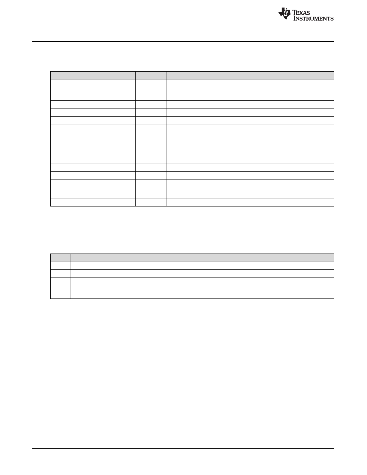
3.3 Layer Information
The 4-layer PCB is used with the configuration, as shown in Table 2.
Layer Usage Notes
1 Signal + RF RF trace is a CPW on L1 w.r.t. L2 ground
2 GND Reference plane for RF
3 Power + signal The power planes for the power amplifier (PA), analog blocks and the main input supply are routed on
4 Power + signal
Table 2. 4 Layer PCB
this layer
6
CC3100 and CC3200 SimpleLink™ Wi-Fi®and Internet of Things Solution
Layout Guidelines
Copyright © 2014–2018, Texas Instruments Incorporated
SWRU370B–June 2014–Revised August 2018
Submit Documentation Feedback
Page 7
www.ti.com
4 Layout Information
The complete layout package is available for download on the TI website at http://www.ti.com/tool/cc3200-
launchxl-rd and http://www.ti.com/tool/cc3100boost-rd. TI recommends that the customers copy the exact
layout of the engine area to ensure optimum performance as measured on the CC3x00 reference boards.
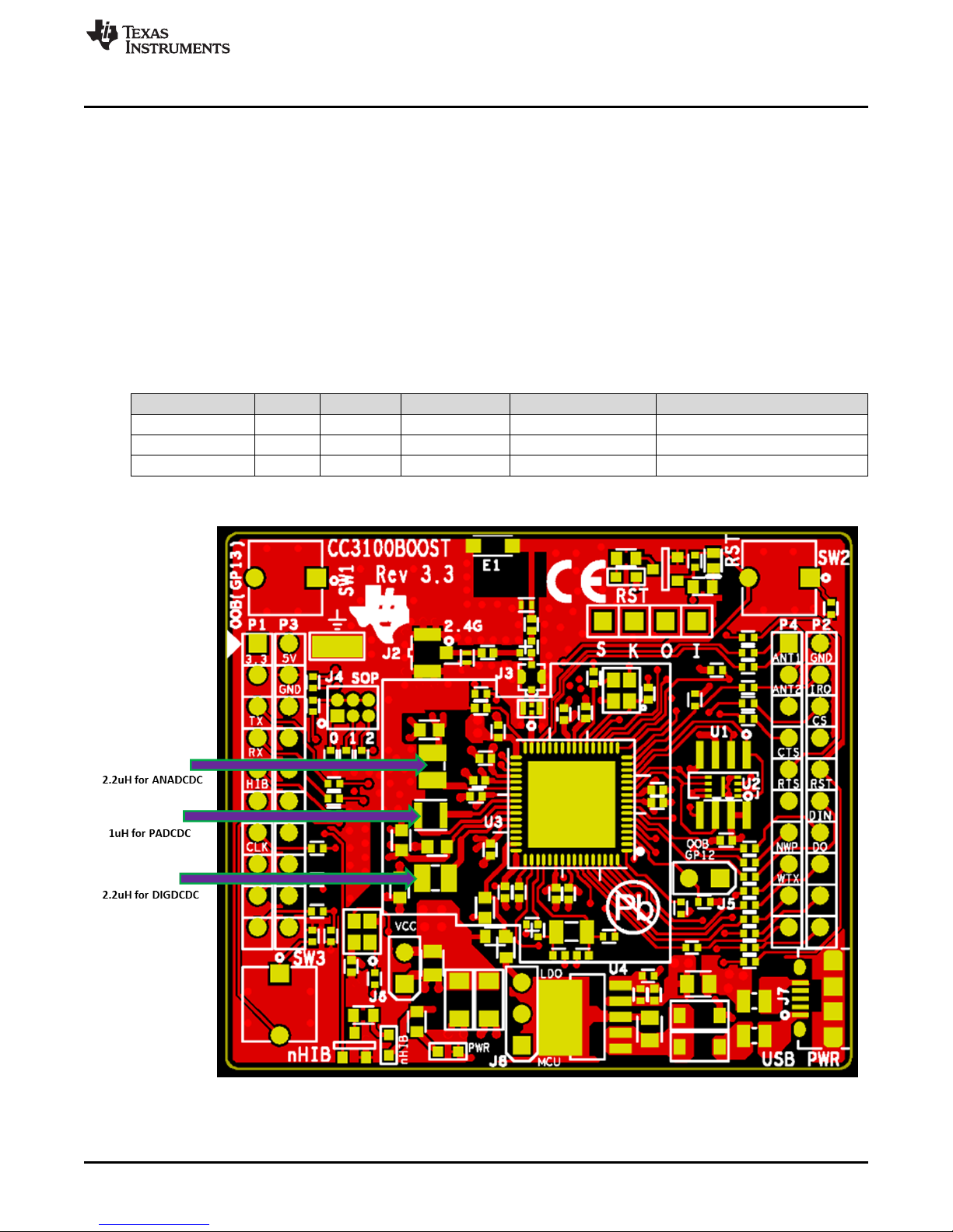
4.1 Placement of Components
The components placement on the CC3100 BoosterPack is provided in Figure 2. This placement provides
optimum performance of the device. Great care must be taken for the power inductors components to
ensure reduced emissions and optimum EVM and mask performance. The power inductors should be
placed close to the device, and the power traces should be minimized. The CC3x00 device is sensitive to
the layout of the DC-DC converter, which can impact the performance of the device. For the main
inductors at the analog, power amplifier, and digital DC-DC output, see Table 3.
Inductor @ Value Size Current Rating Recommended PN Description
ANA DCDC OUT 2.2 µH 1008 1.3A LQM2HPN2R2MG0L INDUCTOR 2.2UH 20% 1008
PA DCDC OUT 1 µH 1008 1.5A LQM2HPN1R0MJ0L INDUCTOR 1UH 20% 1008
DIG DCDC OUT 2.2 µH 1008 1.3A LQM2HPN2R2MG0L INDUCTOR 2.2UH 20% 1008
Figure 2. CC3100BOOST 3.3-A Placement Diagram
Layout Information
Table 3. Inductors
SWRU370B–June 2014–Revised August 2018
Submit Documentation Feedback
CC3100 and CC3200 SimpleLink™ Wi-Fi®and Internet of Things Solution
Copyright © 2014–2018, Texas Instruments Incorporated
Layout Guidelines
7
Page 8

Layout Information
4.2 Layer Information
4.2.1 Layer-1
Most of the routing is performed on Layer-1 to avoid vias on the board (see Figure 3). The trace widths
are maximized for high-current pins and minimized for signal pins. For example, the signal pins can be
routed with 6 mils (4 mils, if possible) and the power pins with 12 mils and above.
www.ti.com
Figure 3. Layer-1
8
CC3100 and CC3200 SimpleLink™ Wi-Fi®and Internet of Things Solution
Layout Guidelines
Copyright © 2014–2018, Texas Instruments Incorporated
SWRU370B–June 2014–Revised August 2018
Submit Documentation Feedback
Page 9

www.ti.com
4.2.2 Layer-2
Layer-2 is primary ground plane for the board reference (see Figure 4). It has a void for the antenna
section, which is per the antenna guidelines. This return current path for the input de-coupling capacitors
(C11, C13, and C18) is routed on L2 using thick traces to isolate RF ground from a noisy supply ground.
This is also required to meet the IEEE spectral mask specifications.
Layout Information
Figure 4. Layer-2
SWRU370B–June 2014–Revised August 2018
Submit Documentation Feedback
CC3100 and CC3200 SimpleLink™ Wi-Fi®and Internet of Things Solution
Copyright © 2014–2018, Texas Instruments Incorporated
Layout Guidelines
9
Page 10

Layout Information
4.2.3 Layer-3
Layer-3 is used to route the power lines to the device (see Figure 5). Power planes are necessary for the
power amplifier (PA) and the main supply input to the device. More details are available in subsequent
sections.
www.ti.com
Figure 5. Layer-3
10
CC3100 and CC3200 SimpleLink™ Wi-Fi®and Internet of Things Solution
Layout Guidelines
Copyright © 2014–2018, Texas Instruments Incorporated
SWRU370B–June 2014–Revised August 2018
Submit Documentation Feedback
Page 11

www.ti.com
4.2.4 Layer-4
Layer-4 is used for routing the power and the signal lines on the board (see Figure 6). It is also the main
power dissipation GND layer for the QFN package. The bottom GND plane must be maximized for the
best thermal performance. The solder mask has been kept open below the QFN device to improve heat
dissipation and yield.
Layout Information
Figure 6. Layer-4
SWRU370B–June 2014–Revised August 2018
Submit Documentation Feedback
CC3100 and CC3200 SimpleLink™ Wi-Fi®and Internet of Things Solution
Copyright © 2014–2018, Texas Instruments Incorporated
Layout Guidelines
11
Page 12

Chip
Antenna
Feed
Void space
on all layers
Antenna
match
Filter
U.FL
conn
Murata
Conn
Layout Guidelines
5 Layout Guidelines
5.1 RF
As a wireless device, the RF section gets the top priority in terms of layout (see Figure 7). It is very
important for the RF section to be laid out correctly to get the optimum performance from the device. A
poor layout can cause performance degradation for the output power, the error vector magnitude (EVM),
the sensitivity, and the spectral mask.
www.ti.com
Figure 7. RF Section Layout
12
CC3100 and CC3200 SimpleLink™ Wi-Fi®and Internet of Things Solution
Layout Guidelines
Copyright © 2014–2018, Texas Instruments Incorporated
SWRU370B–June 2014–Revised August 2018
Submit Documentation Feedback
Page 13

www.ti.com
5.1.1 Antenna Placement and Routing
The antenna is the element used to convert the guided waves on the PCB traces to the free-space
electromagnetic radiation. The placement and layout of the antenna is key to increased range and data
rates.
The guidelines in Table 4 must be observed for the antenna.
Sr No Guidelines
1 Place the antenna on an edge or corner of the PCB.
2 Ensure that no signals are routed across the antenna elements on all the layers of the PCB.
3 Most antennas, including the chip antenna used on the BoosterPack, require ground clearance on all the layers of the
PCB. Ensure that the ground is cleared on the inner layers as well.
4 Ensure that there is provision to place matching components for the antenna. These must be tuned for best return loss
once the complete board is assembled.
Any plastics or casing should also be mounted while tuning the antenna, as this can impact the impedance.
5 Ensure that the antenna impedance is 50 Ω, as the device is rated to work only with a 50-Ω system.
6 In case of printed antenna, ensure that the simulation is performed with the solder mask in consideration.
7 Ensure that the antenna has a near omni-directional pattern.
8 The return loss measured at the filter out (looking into the device) should be better than -10 dB. To ease the FCC, CE, and
ETSI certification, the antenna used should be of the same gain or lesser.
Table 5. Recommended Components
Layout Guidelines
Table 4. Antenna Guidelines
Choice Part Number Manufacturer Notes
1 AH316M245001-T Taiyo Yuden Can be placed on the edge of the PCB and uses less PCB space
2 RFANT5220110A2T Walsim Must be placed on the corner of the PCB
Table 6. Characteristic of Recommended Antenna
Parameter Spec
Frequency bandwidth 2.4G to 2.5G
Typical peak gain +1.9 dBi
Average gain at OMNI plane 0 dBi
Efficiency (typical) –1.3 dB (73%)
VSWR 3
5.1.2 Filter Placement and Routing
The RF filter used on the board performs the important function of attenuating the out-of-band emissions
from the device. The recommended filter is DEA202450BT-1294C1. The datasheet for the filter can be
accessed at http://www.tdk.co.jp/tefe02/rf_bpf_dea202450bt-1294c1-h_en.pdf.
SWRU370B–June 2014–Revised August 2018
Submit Documentation Feedback
CC3100 and CC3200 SimpleLink™ Wi-Fi®and Internet of Things Solution
Copyright © 2014–2018, Texas Instruments Incorporated
Layout Guidelines
13
Page 14

Filter
Layout Guidelines
www.ti.com
Figure 8. Filter Routing
Table 7. Filter Guidelines
Sr No Guidelines Notes
1 Route the RF lines at the input and output of the filter using a coplanar
waveguide (CPW) with ground structure. This structure offers the best
isolation between input and output due to reduced field fringing.
2 Use via stitching along the RF trace to reduce emissions and keep the fields
confined to the trace boundary.
3 Use a Zo of 50 Ω only with a tolerance of 10%. Use the stack-up and the
trace width provided for reference in the PCB design rules.
4 Add multiple ground vias for the filter ground pads as close as possible.
Minimum of 2 per GND pad is recommended.
5 To achieve the specifications of the filter attenuation, the minimum isolation
between input and output ports of the filter must be at least 60 dB. (Measured
without filter)
6 In case a conducted test is required on the PCB, TI recommends adding a
U.FL connector or a Murata switch type connector (MM8030 series).
CPW with GND and via stitching can be
accurately simulated using 3D EM tools
like EESOF.
14
CC3100 and CC3200 SimpleLink™ Wi-Fi®and Internet of Things Solution
Layout Guidelines
SWRU370B–June 2014–Revised August 2018
Submit Documentation Feedback
Copyright © 2014–2018, Texas Instruments Incorporated
Page 15

w
s
e
r
S W S
h
www.ti.com
Parameter Frequency (MHz) Spec
Return loss 2412-2484 10 dB (min)
Insertion loss 2412-2484 1.5 dB (max)
Attenuation
Reference impedance 2412-2484 50 Ω
Filter type Band pass
5.1.3 Transmission Line
The RF signal from the device is routed to the antenna using a coplanar waveguide with ground (CPW-G)
structure. This structure offers the maximum isolation across filter gap and the best possible shielding to
the RF lines. In addition to the ground on the L1 layer, placing GND vias along the line also provides
additional shielding.
Layout Guidelines
Table 8. Characteristic of Recommended Filter
800-830 30 dB (min)
1600-1670 20 dB (min)
3200-3300 30 dB (min)
4000-4150 45 dB (min)
4800-5000 20 dB (min)
5600- 5800 20 dB (min)
6400-6600 20 dB (min)
7200-7500 35 dB (min)
7500-10000 20 dB (min)
Figure 9. Coplanar Waveguide (Cross Section) With GND and via Stitching
Figure 10. CPW With GND (Top View)
SWRU370B–June 2014–Revised August 2018
Submit Documentation Feedback
CC3100 and CC3200 SimpleLink™ Wi-Fi®and Internet of Things Solution
Copyright © 2014–2018, Texas Instruments Incorporated
Layout Guidelines
15
Page 16

Layout Guidelines
The recommended values for the PCB are provided in Table 9.
(1)
Er is assumed to be of an FR-4 substrate.
5.2 Power
• All of the input de-coupling capacitors (C11, C13, and C18) should be routed on L2 using thick traces
to isolate RF ground from a noisy supply ground. This is also required to meet the IEEE spectral mask
specifications.
• Maintain the thickness of power traces to be higher than 12 mils. Special care should be taken for
power amplifier supply lines (pin 33, 40, 41, and 42) and all input supply pins (pin 37, 39, and 44).
• Ensure shortest grounding loop for PLL supply de-coupling capacitor (pin 24)
• Place all de-coupling capacitors as close as possible to the respective pins.
• Power budget: The CC3X00 device can consume up to 450 mA for 3.3 V, 670 mA for 2.1 V, and 700
mA for 1.85 V for 24 msec during the calibration cycle. Ensure that the power supply is designed to
source this current without any issues. The complete calibration (TX and RX) can take up to 17 mJ of
energy from the battery over a time of 24 ms.
• There are many high-current input pins on the CC3X00 device. Ensure the trace feeding these pins is
capable of handling the following currents:
– PA DCDC input : pin 39. Max 1A
– ANA DCDC input : pin 37 : Max 600 mA
– Dig DCDC input : pin 44: Max 500 mA
– PA DCDC switching nodes : pin 40/41 , Max 1A
– PA DCDC output node: pin 42, Max 1A
– ANA DCDC switching node: pin 38: Max 600 mA
– Dig DCDC switching node: pin 43 : Max 500 mA
– PA supply : pin 33: Max 500mA
Table 9. Recommended Values for the PCB
Parameter Value Units
W 18 mils
S 15 mils
H 10 mils
(1)
Er
3.9
www.ti.com
5.2.1 Inductors for Power Management
The components used in the power management section of the design are critical to achieve the required
performance. These should be chosen based on the recommendations in Table 10.
Inductors Value ESR
PA DC-DC 1 uH TBD 1.5 TBD 20%
ANA, DIG DC-DC 2.2 uH TBD 1.3 TBD 20%
16
CC3100 and CC3200 SimpleLink™ Wi-Fi®and Internet of Things Solution
Layout Guidelines
Table 10. Power Management
(mOhm) Rated Current (A)
min
Copyright © 2014–2018, Texas Instruments Incorporated
Saturation
Current I
SWRU370B–June 2014–Revised August 2018
sat
Submit Documentation Feedback
Tolerance
Page 17

www.ti.com
5.3 Clock
5.3.1 32K RTC
The 32.768K XTAL should be placed close to the QFN package. Ensure the load capacitance is tuned
based on board parasitic, so that the frequency tolerance is within ±150 ppm.
Tolerance with temperature and aging ±150 ppm
5.3.2 40M XTAL
The 40M XTAL should be placed close to the QFN package. Ensure the load capacitance is tuned based
on board parasitic, so that the frequency tolerance is within ±20 ppm. The frequency tolerance for the
XTAL across temperature and with aging should be ±25 ppm. In addition, ensure no high frequency lines
are routed closer to the XTAL routing, to avoid any phase noise degradation.
Tolerance with temperature and aging ±25 ppm
Layout Guidelines
Table 11. Characteristic of Recommended 32K XTAL
Parameter Spec
Nominal frequency 32.768 kHz
Table 12. Characteristic of Recommended 40M XTAL
Parameter Spec
Nominal frequency 40 MHz
Tolerance ±20 ppm
Load capacitance 8 pF
5.4 Digital I/O
Route serial peripheral interface (SPI) and universal asynchronous receiver/transmitter (UART) lines away
from any RF traces, as these digital I/O lines are high-frequency lines and can cause interference to the
RF signal.
Keep the length of the high-speed lines as short as possible to avoid transmission line effects. Keep the
line lower than 1/10th of the rise time of the signal to ignore transmission line effects. This is required only
if the traces cannot be kept short. The resistor should be placed at the source end, closer to the device
driving the signal.
Add series-terminating resistors for each high-speed line (for example, SPI_CLK, SPI_DATA) to match the
driver impedance to the line. Typical terminating resistor values range from 27 to 36 Ω for a 50-Ω line
impedance.
Route high-speed lines with a ground reference plane continuously below it to offer good impedance
throughout, and help shield the trace against EMI interference.
Avoid stubs on high speed lines to minimize the reflections. If the line needs to be routed to multiple
locations, use a separate line driver for each line.
If the lines are longer compared to the rise time, add series-terminating resistors near the driver for each
high-speed line (for example, SPI_CLK, SPI_DATA) to match the driver impedance to the line. Typical
terminating resistor values range from 27 to 36 Ω for a 50-Ω line impedance.
SWRU370B–June 2014–Revised August 2018
Submit Documentation Feedback
CC3100 and CC3200 SimpleLink™ Wi-Fi®and Internet of Things Solution
Copyright © 2014–2018, Texas Instruments Incorporated
Layout Guidelines
17
Page 18

Layout Guidelines
5.5 QFN Ground
1. Ensure 7x7 ground vias are placed on the ground pad for optimal thermal dissipation (see Figure 11).
The via drill size can be between 8 mils to 12 mils.
www.ti.com
Figure 11. 7x7 Ground Vias on Ground Pad
2. Open the solder mask on L4 for better soldering yield.
3. Split solder paste into smaller blocks (see Figure 12) to avoid component lifting while soldering or reflow.
Figure 12. Split Solder Paste Into Smaller Blocks
4. Solder paste should cover at-least 75% of the ground tab of the QFN.
18
CC3100 and CC3200 SimpleLink™ Wi-Fi®and Internet of Things Solution
Layout Guidelines
Copyright © 2014–2018, Texas Instruments Incorporated
SWRU370B–June 2014–Revised August 2018
Submit Documentation Feedback
Page 19

www.ti.com
5.6 Recommended Footprint
Layout Guidelines
Figure 13. Recommended Footprint
SWRU370B–June 2014–Revised August 2018
Submit Documentation Feedback
CC3100 and CC3200 SimpleLink™ Wi-Fi®and Internet of Things Solution
Copyright © 2014–2018, Texas Instruments Incorporated
Layout Guidelines
19
Page 20

Summary
6 Summary
This document presents an introduction to designing a 4-layer PCB board for the CC3100/CC3200
SimpleLink Wi-Fi easy-to-layout QFN packaged family of devices. In addition to the recommendations
presented here, see the CC3100 SimpleLink Wi-Fi and IoT Solution BoosterPack design files located at
http://www.ti.com/lit/zip/swrc288 and the CC3200 SimpleLink Wi-Fi and IoT Solution With MCU
LaunchPad board design files located at http://www.ti.com/lit/zip/swrc289.
7 Additional References
1. CC31xx and CC32xx main landing page.
2. The CC3100 SimpleLink™ Wi-Fi® and IoT Solution for MCU Applications data sheet (SWAS031)
3. The CC3200 SimpleLink™ Wi-Fi® and IoT Solution, a Single Chip Wireless MCU data sheet
(SWAS032)
www.ti.com
20
CC3100 and CC3200 SimpleLink™ Wi-Fi®and Internet of Things Solution
Layout Guidelines
Copyright © 2014–2018, Texas Instruments Incorporated
SWRU370B–June 2014–Revised August 2018
Submit Documentation Feedback
Page 21

www.ti.com
Revision History
Revision History
NOTE: Page numbers for previous revisions may differ from page numbers in the current version.
Changes from A Revision (September 2014) to B Revision .......................................................................................... Page
• Updated Schematic Checklist link....................................................................................................... 4
• Updated References..................................................................................................................... 20
SWRU370B–June 2014–Revised August 2018
Submit Documentation Feedback
Copyright © 2014–2018, Texas Instruments Incorporated
Revision History
21
Page 22

IMPORTANT NOTICE FOR TI DESIGN INFORMATION AND RESOURCES
Texas Instruments Incorporated (‘TI”) technical, application or other design advice, services or information, including, but not limited to,
reference designs and materials relating to evaluation modules, (collectively, “TI Resources”) are intended to assist designers who are
developing applications that incorporate TI products; by downloading, accessing or using any particular TI Resource in any way, you
(individually or, if you are acting on behalf of a company, your company) agree to use it solely for this purpose and subject to the terms of
this Notice.
TI’s provision of TI Resources does not expand or otherwise alter TI’s applicable published warranties or warranty disclaimers for TI
products, and no additional obligations or liabilities arise from TI providing such TI Resources. TI reserves the right to make corrections,
enhancements, improvements and other changes to its TI Resources.
You understand and agree that you remain responsible for using your independent analysis, evaluation and judgment in designing your
applications and that you have full and exclusive responsibility to assure the safety of your applications and compliance of your applications
(and of all TI products used in or for your applications) with all applicable regulations, laws and other applicable requirements. You
represent that, with respect to your applications, you have all the necessary expertise to create and implement safeguards that (1)
anticipate dangerous consequences of failures, (2) monitor failures and their consequences, and (3) lessen the likelihood of failures that
might cause harm and take appropriate actions. You agree that prior to using or distributing any applications that include TI products, you
will thoroughly test such applications and the functionality of such TI products as used in such applications. TI has not conducted any
testing other than that specifically described in the published documentation for a particular TI Resource.
You are authorized to use, copy and modify any individual TI Resource only in connection with the development of applications that include
the TI product(s) identified in such TI Resource. NO OTHER LICENSE, EXPRESS OR IMPLIED, BY ESTOPPEL OR OTHERWISE TO
ANY OTHER TI INTELLECTUAL PROPERTY RIGHT, AND NO LICENSE TO ANY TECHNOLOGY OR INTELLECTUAL PROPERTY
RIGHT OF TI OR ANY THIRD PARTY IS GRANTED HEREIN, including but not limited to any patent right, copyright, mask work right, or
other intellectual property right relating to any combination, machine, or process in which TI products or services are used. Information
regarding or referencing third-party products or services does not constitute a license to use such products or services, or a warranty or
endorsement thereof. Use of TI Resources may require a license from a third party under the patents or other intellectual property of the
third party, or a license from TI under the patents or other intellectual property of TI.
TI RESOURCES ARE PROVIDED “AS IS” AND WITH ALL FAULTS. TI DISCLAIMS ALL OTHER WARRANTIES OR
REPRESENTATIONS, EXPRESS OR IMPLIED, REGARDING TI RESOURCES OR USE THEREOF, INCLUDING BUT NOT LIMITED TO
ACCURACY OR COMPLETENESS, TITLE, ANY EPIDEMIC FAILURE WARRANTY AND ANY IMPLIED WARRANTIES OF
MERCHANTABILITY, FITNESS FOR A PARTICULAR PURPOSE, AND NON-INFRINGEMENT OF ANY THIRD PARTY INTELLECTUAL
PROPERTY RIGHTS.
TI SHALL NOT BE LIABLE FOR AND SHALL NOT DEFEND OR INDEMNIFY YOU AGAINST ANY CLAIM, INCLUDING BUT NOT
LIMITED TO ANY INFRINGEMENT CLAIM THAT RELATES TO OR IS BASED ON ANY COMBINATION OF PRODUCTS EVEN IF
DESCRIBED IN TI RESOURCES OR OTHERWISE. IN NO EVENT SHALL TI BE LIABLE FOR ANY ACTUAL, DIRECT, SPECIAL,
COLLATERAL, INDIRECT, PUNITIVE, INCIDENTAL, CONSEQUENTIAL OR EXEMPLARY DAMAGES IN CONNECTION WITH OR
ARISING OUT OF TI RESOURCES OR USE THEREOF, AND REGARDLESS OF WHETHER TI HAS BEEN ADVISED OF THE
POSSIBILITY OF SUCH DAMAGES.
You agree to fully indemnify TI and its representatives against any damages, costs, losses, and/or liabilities arising out of your noncompliance with the terms and provisions of this Notice.
This Notice applies to TI Resources. Additional terms apply to the use and purchase of certain types of materials, TI products and services.
These include; without limitation, TI’s standard terms for semiconductor products http://www.ti.com/sc/docs/stdterms.htm), evaluation
modules, and samples (http://www.ti.com/sc/docs/sampterms.htm).
Mailing Address: Texas Instruments, Post Office Box 655303, Dallas, Texas 75265
Copyright © 2018, Texas Instruments Incorporated
 Loading...