PA
Logic
Bias
15 7
2
3
4
11
LNA
5
6
BIAS
HGM
RF_P
RXTX
RF_N
PAEN
EN
BALUN
ANT
CC2591
www.ti.com
........................................................................................................................................................ SWRS070A – MARCH 2008 – REVISED JUNE 2008
2.4-GHz RF Front End
1
FEATURES APPLICATIONS
• Seamless Interface to 2.4-GHz Low Power RF
Devices from Texas Instruments
• Up to 22-dBm Output Power
• 6-dB Typical Improved Sensitivity on CC24xx
and CC2500, CC2510, and CC2511
• Few External Components
– Integrated Switches
– Integrated Matching Network
– Integrated Balun
– Integrated Inductors
– Integrated PA
– Integrated LNA
• Digital Control of LNA Gain by HGM Pin System-on-Chip products from Texas Instruments.
• 100-nA in Power Down (EN = PAEN = 0)
• Low Transmit Current Consumption
(100-mA at 3-V for 20-dBm Out, PAE = 33%)
• Low Receive Current Consumption
– 3.4-mA for High Gain Mode
– 1.7-mA for Low Gain Mode
• 4.8-dB LNA Noise Figure, including T/R Switch
and external antenna match
• RoHS Compliant 4 × 4-mm QFN-16 Package
• 2-V to 3.6-V Operation
• All 2.4-GHz ISM Band Systems
• Wireless Sensor Networks
• Wireless Industrial Systems
• IEEE 802.15.4 and ZigBee Systems
• Wireless Consumer Systems
• Wireless Audio Systems
DESCRIPTION
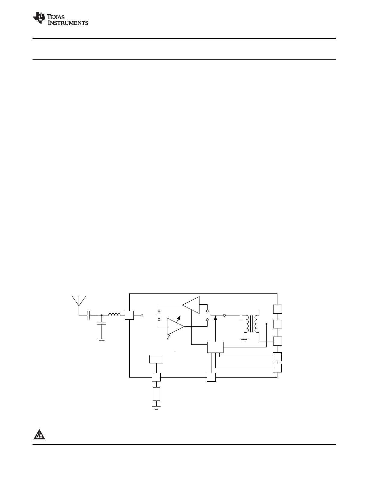
CC2591 is a cost-effective and high performance RF
Front End for low-power and low-voltage 2.4-GHz
wireless applications.
CC2591 is a range extender for all existing and future
2.4-GHz low-power RF transceivers, transmitters and
CC2591 increases the link budget by providing a
power amplifier for increased output power, and an
LNA with low noise figure for improved receiver
sensitivity.
CC2591 provides a small size, high output power RF
design with its 4x4-mm QFN-16 package.
CC2591 contains PA, LNA, switches, RF-matching,
and balun for simple design of high performance
wireless applications.
CC2591 BLOCK DIAGRAM
1
Please be aware that an important notice concerning availability, standard warranty, and use in critical applications of Texas Instruments semiconductor products and disclaimers thereto appears at the end of this data sheet.
Submit Documentation Feedback Copyright © 2008, Texas Instruments Incorporated
CC2591
SWRS070A – MARCH 2008 – REVISED JUNE 2008 ........................................................................................................................................................
These devices have limited built-in ESD protection. The leads should be shorted together or the device placed in conductive foam
during storage or handling to prevent electrostatic damage to the MOS gates.
ABSOLUTE MAXIMUM RATINGS
Under no circumstances must the absolute maximum ratings be violated. Stress exceeding one or more of the limiting values
may cause permanent damage to the device.
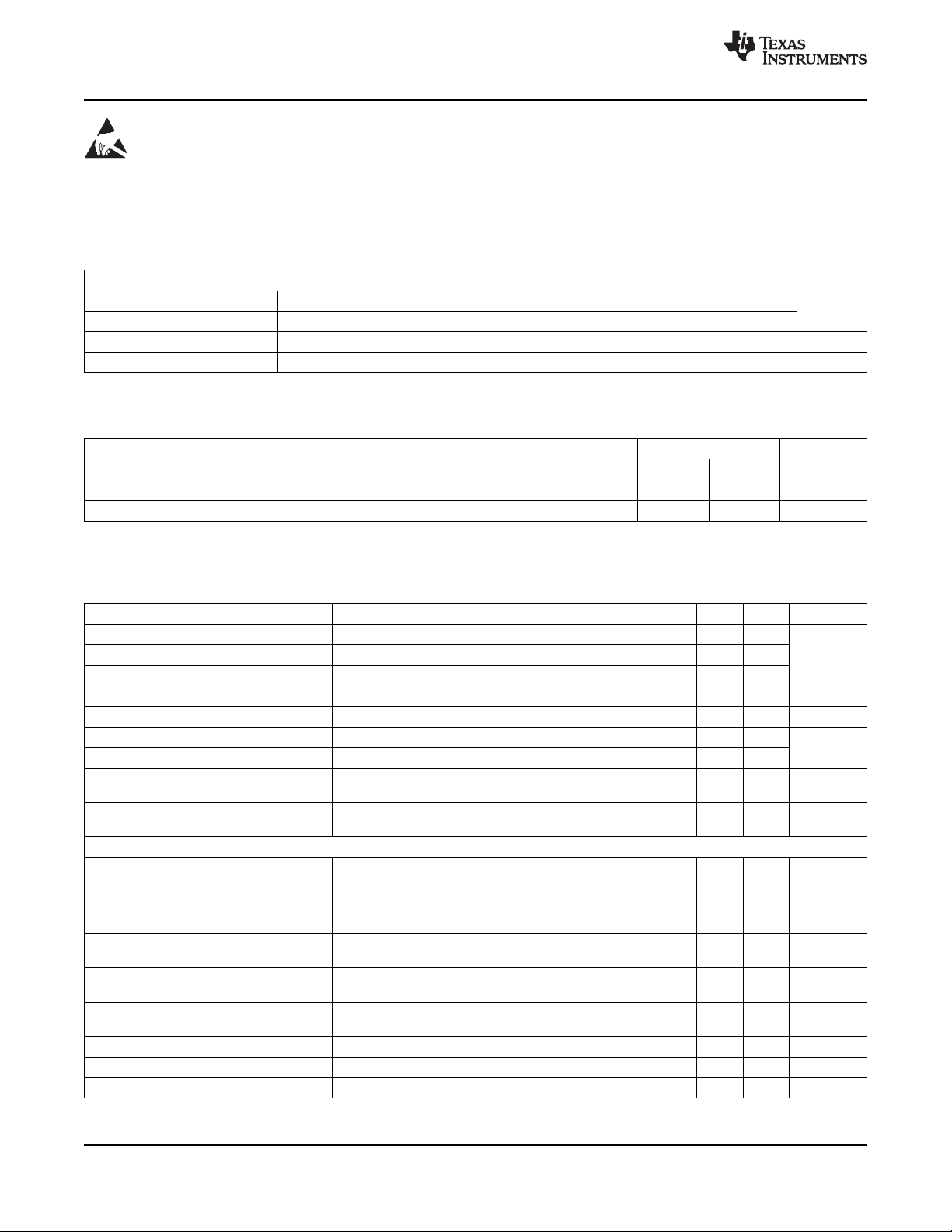
PARAMETER VALUE UNIT
Supply voltage All supply pins must have the same voltage – 0.3 to 3.6
Voltage on any digital pin – 0.3 to V
Input RF level 10 dBm
Storage temperature range – 50 to 150 ° C
DD
+ 0.3, max 3.6
RECOMMENDED OPERATING CONDITIONS
The operating conditions for CC2591 are listed below.
PARAMETER MIN MAX UNIT
Ambient temperature range – 40 85 ° C
Operating supply voltage 2 3.6 V
Operating frequency range 2400 2483.5 MHz
www.ti.com
V
ELECTRICAL CHARACTERISTICS
TC= 25 ° C, V
matching components.
Receive current, High Gain Mode HGM = 1 3.4 4
Receive current, Low Gain Mode HGM = 0 1.7 2
Transmit current PIN= 0.5 dBm 112
Transmit current No input signal 40 50
Power down current EN = PAEN = 0 0.1 0.3 µ A
High input level (control pins) EN, PAEN, HGM, RXTX 1.3 V
Low input level (control pins) EN, PAEN, HGM, RXTX 0.3
Power down - Receive mode switching
time
Power down - Transmit mode switching
time
RF Receive
Gain, High Gain Mode HGM = 1 11 dB
Gain, Low Gain Mode HGM = 0 1 dB
Gain variation, 2400 – 2483.5 MHz, High
Gain Mode
Gain variation, 2.0V – 3.6V, High Gain
Mode
Gain variation, -40 ° C – 85 ° C, High Gain
Mode
Noise figure, High Gain Mode 4.8 dB
Input 1 dB compression, High Gain Mode HGM = 1 – 17 dBm
Input IP3, High Gain Mode HGM = 1 – 2 dBm
Input reflection coefficient, S11 HGM = 1, measured at antenna port – 11 dB
= 3 V , fRF= 2440MHz (unless otherwise noted). Measured on CC2591EM reference design including external
DD
PARAMETER TEST CONDITIONS MIN TYP MAX UNIT
12 µ s
1 µ s
HGM = 1 1.3 dB
HGM = 1 1.5 dB
HGM = 1 3 dB
HGM = 1, including internal T/R switch and external
antenna match
DD
mA
V
2 Submit Documentation Feedback Copyright © 2008, Texas Instruments Incorporated
Product Folder Link(s): CC2591
CC2591
www.ti.com
........................................................................................................................................................ SWRS070A – MARCH 2008 – REVISED JUNE 2008
ELECTRICAL CHARACTERISTICS (continued)
TC= 25 ° C, V
matching components.
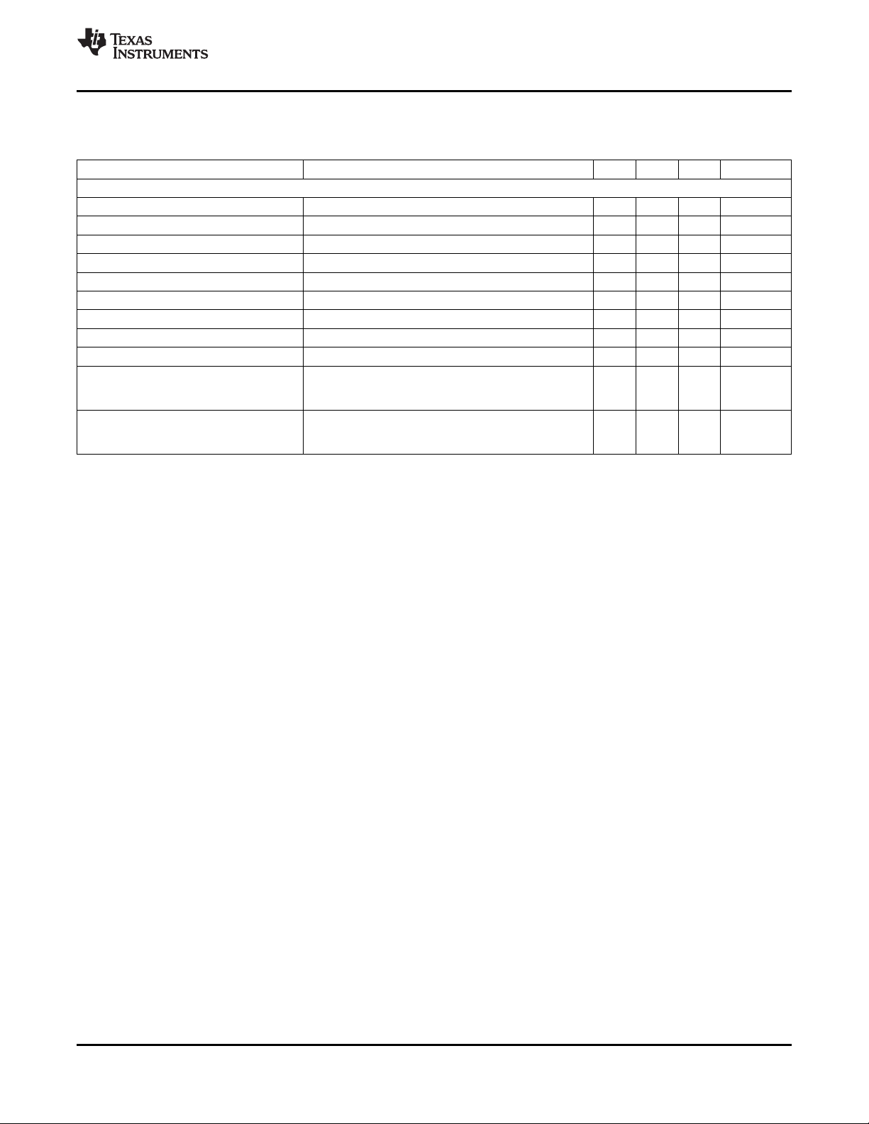
RF Transmit
Gain 22 dB
Output power, P
Maximum output power PIN= 5 dBm 22 dBm
Power Added Efficiency, PAE PIN= 0.5 dBm 34%
Output 1 dB compression 19 dBm
Output IP3 32 dBm
Output power variation over frequency 2400 – 2483.5 MHz, PIN= 0.5 dBm 0.5 dB
Output power variation over power supply 2V – 3.6V , PIN= 0.5 dBm 3.5 dB
Output power variation over temperature -40 ° C – 85 ° C, PIN= 0.5 dBm 1.5 dB
2nd harmonic power below regulatory limits by using an external LC filter – 15 dBm
3rd harmonic power below regulatory limits by using an external LC filter – 30 dBm
= 3 V , fRF= 2440MHz (unless otherwise noted). Measured on CC2591EM reference design including external
DD
PARAMETER TEST CONDITIONS MIN TYP MAX UNIT
OUT
PIN= 0.5 dBm 20.6 dBm
PIN= 0.5 dBm. The 2nd harmonic can be reduced to
and antenna.
PIN= 0.5 dBm. The 3rd harmonic can be reduced to
and antenna.
Copyright © 2008, Texas Instruments Incorporated Submit Documentation Feedback 3
Product Folder Link(s): CC2591
AVDD_PA1
1
2
3
4
12
11
10
9
5 6 7 8
16 15 14 13
QFN-16 4x4mm
RF_N
RXTX
RF_P
HGM
EN
PAEN
GND
GND
ANT
GND
AVDD_BIAS
BIAS
GND
AVDD_LNA
AVDD_PA2
CC2591
SWRS070A – MARCH 2008 – REVISED JUNE 2008 ........................................................................................................................................................
DEVICE INFORMATION
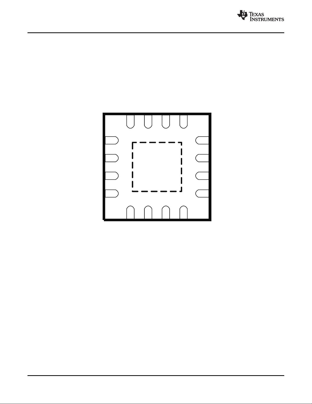
The CC2591 pinout and description are shown in Figure 1 and Table 1 , respectively.
PIN AND I/O CONFIGURATION
(TOP VIEW)
www.ti.com
4 Submit Documentation Feedback Copyright © 2008, Texas Instruments Incorporated
The exposed die attach pad must be connected to a solid ground plane as this is the
primary ground connection for the chip. Inductance in vias to the pad should be
minimized. It is highly recommended to follow the reference layout. Changes will alter
the performance. Also see the PCB landpattern information in this data sheet.
For best performance, minimize the length of the ground vias, by using a 4-layer PCB
with ground plane as layer 2 when CC2591 is mounted onto layer 1.
Figure 1.
NOTE:
Product Folder Link(s): CC2591

CC2591
www.ti.com
........................................................................................................................................................ SWRS070A – MARCH 2008 – REVISED JUNE 2008
Table 1. TERMINAL FUNCTIONS
TERMINAL
NO. NAME
— GND Ground
1 2.0 V – 3.6 V Power. PCB trace to this pin serves as inductive load to PA . See
2 RF_N RF RF interface towards CC24xx or CC25xx device.
3 RXTX Analog/Control
4 RF_P RF RF interface towards CC24xx or CC25xx device
5 PAEN Digital Input Digital control pin. See Table 3 and Table 4 for details.
6 EN Digital Input Digital control pin. See Table 3 and Table 4 for details.
7 HGM Digital Input HGM=1 → Device in High Gain Mode
8, 9, 12, 14 GND Ground
10 AVDD_PA2 Power
11 ANT RF Antenna interface.
13 AVDD_LNA Power
15 BIAS Analog Biasing input. Resistor between this node and ground sets bias current to PAs.
16 AVDD_BIAS Power 2 V – 3.6 V Power.
AVDD_PA1 Power
TYPE DESCRIPTION
The exposed die attach pad must be connected to a solid ground plane. See
CC2591EM reference design for recommended layout.
CC2591EM reference design for recommended layout.
RXTX switching voltage when connected to CC24xx devices. See Table 3 and Table 4
for details.
Digital control pin.
HGM=0 → Device in Low Gain Mode (RX only)
Secondary ground connections. Should be shorted to the die attach pad on the top
PCB layer.
2.0 V – 3.6 V Power. PCB trace to this pin serves as inductive load to PA. See
CC2591EM reference design for recommended layout.
2 V – 3.6 V Power. PCB trace to this pin serves as inductive load to LNA. See
CC2591EM reference design for recommended layout.
Copyright © 2008, Texas Instruments Incorporated Submit Documentation Feedback 5
Product Folder Link(s): CC2591
RF_P
RXTX
RF_N
RF_P
RXTX
RF_N
= TLINE inductor
CC2591
ANT
PAEN
EN
HGM
BIAS
VDD
AVDD_PA2
AVDD_PA1
AVDD_LNA
AVDD_BIAS
VDD VDD
VDD
RF_P
RXTX
RF_N
R151
TL11
TL101
TL131
PAEN
EN
C111
L112
C161
C11/C12
C101/C102
C131/C132
HGM
RXTX
C2
LDB182G4520C-110
Balun
SMA
SMA
L111
CC2591
SWRS070A – MARCH 2008 – REVISED JUNE 2008 ........................................................................................................................................................
CC2591EM Evaluation Module
www.ti.com
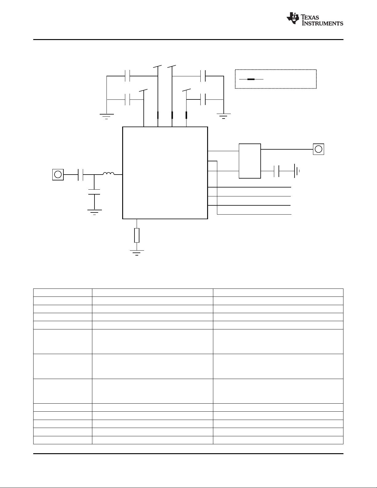
Figure 2. CC2591EM Evaluation Module
Table 2. List of Materials (See CC2591EM Reference Design)
DEVICE FUNCTION VALUE
L112 Part of antenna match. 1.5 nH: LQW15AN1N5B00 from Murata
L111 DC block. 1 nF: GRM1555C1H102JA01 from Murata
C111 Part of antenna match. 1 pF: GRM1555C1H1R0BZ01 from Murata
C161 Decoupling capacitor. 1 nF: GRM1555C1H102JA01 from Murata
C11/C12 Decoupling. Will affect PA resonance.
C101/C102 Decoupling. Will affect PA resonance.
C131/C132 Decoupling. Will affect PA resonance.
C2 Decoupling of external balun 1 nF: GRM1555C1H102JA01 from Murata
TL11 Transmission line. Will affect PA resonance. See CC2591EM reference design.
TL101 Transmission line. Will affect PA resonance. See CC2591EM reference design.
TL131 Transmission line. Will affect LNA resonance. See CC2591EM reference design.
R151 Bias resistor 4.3 k Ω : RK73H1ETTP4301F from Koa
10 pF || 1 nF. The smallest cap closest. See CC2591EM
reference design for placement.
10 pF: GRM1555C1H100JZ01 from Murata
1 nF: GRM1555C1H102JA01 from Murata
18 pF || 1 nF. The smallest cap closest. See for
CC2591EM reference design placement.
18 pF: GRM1555C1H180JZ01 from Murata
1 nF: GRM1555C1H102JA01 from Murata
10 pF || 1 nF. The smallest cap closest. See CC2591EM
reference design for placement.
10 pF: GRM1555C1H100JZ01 from Murata
1 nF: GRM1555C1H102JA01 from Murata
6 Submit Documentation Feedback Copyright © 2008, Texas Instruments Incorporated
Product Folder Link(s): CC2591
 Loading...