

Page 1

CC253x System-on-Chip Solution for 2.4-GHz
IEEE 802.15.4 and ZigBee®Applications
A
CC2540/41 System-on-Chip Solution for 2.4GHz Bluetooth®low energy Applications
User's Guide
Literature Number: SWRU191F
April 2009–Revised April 2014
Page 2

Contents
Preface....................................................................................................................................... 14
1 Introduction....................................................................................................................... 17
1.1 Overview..................................................................................................................... 18
1.1.1 CPU and Memory ................................................................................................. 21
1.1.2 Clocks and Power Management ................................................................................ 21
1.1.3 Peripherals ......................................................................................................... 21
1.1.4 Radio................................................................................................................ 23
1.2 Applications ................................................................................................................. 23
2 8051 CPU........................................................................................................................... 24
2.1 8051 CPU Introduction .................................................................................................... 25
2.2 Memory...................................................................................................................... 25
2.2.1 Memory Map....................................................................................................... 25
2.2.2 CPU Memory Space .............................................................................................. 27
2.2.3 Physical Memory .................................................................................................. 28
2.2.4 XDATA Memory Access.......................................................................................... 33
2.2.5 Memory Arbiter .................................................................................................... 33
2.3 CPU Registers.............................................................................................................. 34
2.3.1 Data Pointers ...................................................................................................... 34
2.3.2 Registers R0–R7 .................................................................................................. 35
2.3.3 Program Status Word............................................................................................. 35
2.3.4 Accumulator........................................................................................................ 36
2.3.5 B Register .......................................................................................................... 36
2.3.6 Stack Pointer....................................................................................................... 36
2.4 Instruction Set Summary .................................................................................................. 36
2.5 Interrupts .................................................................................................................... 40
2.5.1 Interrupt Masking.................................................................................................. 41
2.5.2 Interrupt Processing............................................................................................... 45
2.5.3 Interrupt Priority.................................................................................................... 47
3 Debug Interface.................................................................................................................. 50
3.1 Debug Mode ................................................................................................................ 51
3.2 Debug Communication .................................................................................................... 51
3.3 Debug Commands ......................................................................................................... 53
3.3.1 Debug Configuration.............................................................................................. 55
3.3.2 Debug Status ...................................................................................................... 55
3.3.3 Hardware Breakpoints ............................................................................................ 56
3.4 Flash Programming ........................................................................................................ 57
3.4.1 Lock Bits............................................................................................................ 57
3.5 Debug Interface and Power Modes...................................................................................... 57
3.6 Registers .................................................................................................................... 59
4 Power Management and Clocks ........................................................................................... 60
4.1 Power Management Introduction......................................................................................... 61
4.1.1 Active and Idle Modes............................................................................................ 62
4.1.2 PM1 ................................................................................................................. 62
4.1.3 PM2 ................................................................................................................. 62
2
Contents SWRU191F–April 2009–Revised April 2014
Copyright © 2009–2014, Texas Instruments Incorporated
Submit Documentation Feedback
Page 3

www.ti.com
4.1.4 PM3 ................................................................................................................. 62
4.2 Power-Management Control.............................................................................................. 62
4.3 Power-Management Registers ........................................................................................... 63
4.4 Oscillators and Clocks ..................................................................................................... 66
4.4.1 Oscillators .......................................................................................................... 66
4.4.2 System Clock ...................................................................................................... 66
4.4.3 32-kHz Oscillators................................................................................................. 67
4.4.4 Oscillator and Clock Registers .................................................................................. 67
4.5 Timer Tick Generation ..................................................................................................... 69
4.6 Data Retention.............................................................................................................. 69
5 Reset ................................................................................................................................ 70
5.1 Power-On Reset and Brownout Detector ............................................................................... 71
5.2 Clock-Loss Detector ....................................................................................................... 71
6 Flash Controller ................................................................................................................. 72
6.1 Flash Memory Organization............................................................................................... 73
6.2 Flash Write .................................................................................................................. 73
6.2.1 Flash-Write Procedure............................................................................................ 73
6.2.2 Writing Multiple Times to a Word ............................................................................... 74
6.2.3 DMA Flash Write .................................................................................................. 74
6.2.4 CPU Flash Write................................................................................................... 75
6.3 Flash Page Erase .......................................................................................................... 75
6.3.1 Performing Flash Erase From Flash Memory ................................................................. 76
6.3.2 Different Flash Page Size on CC2533 ......................................................................... 76
6.4 Flash DMA Trigger ......................................................................................................... 76
6.5 Flash Controller Registers ................................................................................................ 76
7 I/O Ports............................................................................................................................ 78
7.1 Unused I/O Pins ............................................................................................................ 79
7.2 Low I/O Supply Voltage ................................................................................................... 79
7.3 General-Purpose I/O....................................................................................................... 79
7.4 General-Purpose I/O Interrupts........................................................................................... 79
7.5 General-Purpose I/O DMA ................................................................................................ 80
7.6 Peripheral I/O ............................................................................................................... 80
7.6.1 Timer 1.............................................................................................................. 81
7.6.2 Timer 3.............................................................................................................. 81
7.6.3 Timer 4.............................................................................................................. 82
7.6.4 USART 0 ........................................................................................................... 82
7.6.5 USART 1 ........................................................................................................... 82
7.6.6 ADC................................................................................................................. 83
7.6.7 Operational Amplifier and Analog Comparator................................................................ 83
7.7 Debug Interface............................................................................................................. 83
7.8 32-kHz XOSC Input ........................................................................................................ 83
7.9 Radio Test Output Signals................................................................................................ 84
7.10 Power-Down Signal MUX (PMUX)....................................................................................... 84
7.11 I/O Registers................................................................................................................ 84
8 DMA Controller .................................................................................................................. 92
8.1 DMA Operation ............................................................................................................. 93
8.2 DMA Configuration Parameters .......................................................................................... 95
8.2.1 Source Address.................................................................................................... 95
8.2.2 Destination Address............................................................................................... 95
8.2.3 Transfer Count..................................................................................................... 95
8.2.4 VLEN Setting....................................................................................................... 96
8.2.5 Trigger Event....................................................................................................... 96
SWRU191F–April 2009–Revised April 2014 Contents
Submit Documentation Feedback
Copyright © 2009–2014, Texas Instruments Incorporated
3
Page 4

www.ti.com
8.2.6 Source and Destination Increment.............................................................................. 96
8.2.7 DMA Transfer Mode .............................................................................................. 97
8.2.8 DMA Priority........................................................................................................ 97
8.2.9 Byte or Word Transfers........................................................................................... 97
8.2.10 Interrupt Mask .................................................................................................... 97
8.2.11 Mode 8 Setting ................................................................................................... 97
8.3 DMA Configuration Setup ................................................................................................. 97
8.4 Stopping DMA Transfers .................................................................................................. 98
8.5 DMA Interrupts.............................................................................................................. 98
8.6 DMA Configuration-Data Structure....................................................................................... 98
8.7 DMA Memory Access...................................................................................................... 98
8.8 DMA Registers ............................................................................................................ 101
9 Timer 1 (16-Bit Timer)........................................................................................................ 103
9.1 16-Bit Counter............................................................................................................. 104
9.2 Timer 1 Operation ........................................................................................................ 104
9.3 Free-Running Mode ...................................................................................................... 104
9.4 Modulo Mode.............................................................................................................. 105
9.5 Up-and-Down Mode ...................................................................................................... 105
9.6 Channel-Mode Control ................................................................................................... 105
9.7 Input Capture Mode ...................................................................................................... 106
9.8 Output Compare Mode................................................................................................... 106
9.9 IR Signal Generation and Learning .................................................................................... 111
9.9.1 Introduction ....................................................................................................... 111
9.9.2 Modulated Codes ................................................................................................ 111
9.9.3 Non-Modulated Codes .......................................................................................... 112
9.9.4 Learning........................................................................................................... 113
9.9.5 Other Considerations............................................................................................ 113
9.10 Timer 1 Interrupts......................................................................................................... 113
9.11 Timer 1 DMA Triggers.................................................................................................... 113
9.12 Timer 1 Registers......................................................................................................... 114
9.13 Accessing Timer 1 Registers as Array ................................................................................ 119
10 Timer 3 and Timer 4 (8-Bit Timers)...................................................................................... 120
10.1 8-Bit Timer Counter....................................................................................................... 121
10.2 Timer 3 and Timer 4 Mode Control..................................................................................... 121
10.2.1 Free-Running Mode ............................................................................................ 121
10.2.2 Down Mode...................................................................................................... 121
10.2.3 Modulo Mode.................................................................................................... 121
10.2.4 Up-and-Down Mode ............................................................................................ 121
10.3 Channel Mode Control ................................................................................................... 121
10.4 Input Capture Mode ...................................................................................................... 122
10.5 Output Compare Mode................................................................................................... 122
10.6 Timer 3 and Timer 4 Interrupts.......................................................................................... 122
10.7 Timer 3 and Timer 4 DMA Triggers .................................................................................... 123
10.8 Timer 3 and Timer 4 Registers.......................................................................................... 123
11 Sleep Timer...................................................................................................................... 128
11.1 General..................................................................................................................... 129
11.2 Timer Compare ........................................................................................................... 129
11.3 Timer Capture............................................................................................................. 129
11.4 Sleep Timer Registers ................................................................................................... 130
12 ADC ................................................................................................................................ 132
12.1 ADC Introduction.......................................................................................................... 133
12.2 ADC Operation............................................................................................................ 133
4
Contents SWRU191F–April 2009–Revised April 2014
Copyright © 2009–2014, Texas Instruments Incorporated
Submit Documentation Feedback
Page 5

www.ti.com
12.2.1 ADC Inputs ...................................................................................................... 133
12.2.2 ADC Conversion Sequences.................................................................................. 134
12.2.3 Single ADC Conversion........................................................................................ 134
12.2.4 ADC Operating Modes......................................................................................... 134
12.2.5 ADC Conversion Results ...................................................................................... 135
12.2.6 ADC Reference Voltage ....................................................................................... 135
12.2.7 ADC Conversion Timing ....................................................................................... 135
12.2.8 ADC Interrupts .................................................................................................. 135
12.2.9 ADC DMA Triggers............................................................................................. 135
12.2.10 ADC Registers................................................................................................. 136
13 Battery Monitor ................................................................................................................ 139
13.1 Functionality and Usage of the Battery Monitor ...................................................................... 140
13.2 Using the Battery Monitor for Temperature Monitoring.............................................................. 140
13.3 Battery Monitor Registers ............................................................................................... 141
14 Random-Number Generator ............................................................................................... 143
14.1 Introduction ................................................................................................................ 144
14.2 Random-Number-Generator Operation................................................................................ 144
14.2.1 Pseudorandom Sequence Generation....................................................................... 144
14.2.2 Seeding .......................................................................................................... 144
14.2.3 CRC16 ........................................................................................................... 144
14.3 Random-Number-Generator Registers ................................................................................ 145
15 AES Coprocessor ............................................................................................................. 146
15.1 AES Operation ............................................................................................................ 147
15.2 Key and IV ................................................................................................................. 147
15.3 Padding of Input Data.................................................................................................... 147
15.4 Interface to CPU .......................................................................................................... 147
15.5 Modes of Operation ...................................................................................................... 147
15.6 CBC-MAC.................................................................................................................. 147
15.7 CCM Mode................................................................................................................. 148
15.8 AES Interrupts............................................................................................................. 150
15.9 AES DMA Triggers ....................................................................................................... 150
15.10 AES Registers ............................................................................................................ 150
16 Watchdog Timer ............................................................................................................... 152
16.1 Watchdog Mode........................................................................................................... 153
16.2 Timer Mode................................................................................................................ 153
16.3 Watchdog Timer Register................................................................................................ 153
17 USART ............................................................................................................................ 155
17.1 UART Mode ............................................................................................................... 156
17.1.1 UART Transmit.................................................................................................. 156
17.1.2 UART Receive .................................................................................................. 156
17.1.3 UART Hardware Flow Control ................................................................................ 156
17.1.4 UART Character Format....................................................................................... 157
17.2 SPI Mode .................................................................................................................. 157
17.2.1 SPI Master Operation .......................................................................................... 157
17.2.2 SPI Slave Operation............................................................................................ 158
17.3 SSN Slave-Select Pin .................................................................................................... 158
17.4 Baud-Rate Generation ................................................................................................... 158
17.5 USART Flushing .......................................................................................................... 159
17.6 USART Interrupts......................................................................................................... 159
17.7 USART DMA Triggers.................................................................................................... 159
17.8 USART Registers......................................................................................................... 159
18 Operational Amplifier ........................................................................................................ 164
SWRU191F–April 2009–Revised April 2014 Contents
Submit Documentation Feedback
Copyright © 2009–2014, Texas Instruments Incorporated
5
Page 6

www.ti.com
18.1 Description................................................................................................................. 165
18.2 Calibration ................................................................................................................. 165
18.3 Clock Source .............................................................................................................. 165
18.4 Registers................................................................................................................... 165
19 Analog Comparator........................................................................................................... 166
19.1 Description................................................................................................................. 167
19.2 Register .................................................................................................................... 167
20 I
2
C................................................................................................................................... 168
20.1 Operation .................................................................................................................. 169
20.1.1 I
20.1.2 I
20.1.3 I
20.1.4 I
20.1.5 I
2
C Initialization and Reset..................................................................................... 170
2
C Serial Data .................................................................................................. 170
2
C Addressing Modes ......................................................................................... 171
2
C Module Operating Modes ................................................................................. 171
2
C Clock Generation and Synchronization.................................................................. 177
20.1.6 Bus Error......................................................................................................... 178
2
C Interrupt...................................................................................................... 178
2
C Pins........................................................................................................... 178
20.2 I
20.1.7 I
20.1.8 I
2
C Registers............................................................................................................... 178
21 USB Controller ................................................................................................................. 181
21.1 USB Introduction.......................................................................................................... 182
21.2 USB Enable................................................................................................................ 182
21.3 48-MHz USB PLL......................................................................................................... 182
21.4 USB Interrupts............................................................................................................. 183
21.5 Endpoint 0 ................................................................................................................. 183
21.6 Endpoint-0 Interrupts ..................................................................................................... 183
21.6.1 Error Conditions................................................................................................. 184
21.6.2 SETUP Transactions (IDLE State) ........................................................................... 184
21.6.3 IN Transactions (TX State) .................................................................................... 184
21.6.4 OUT Transactions (RX State)................................................................................. 185
21.7 Endpoints 1–5............................................................................................................. 185
21.7.1 FIFO Management ............................................................................................. 185
21.7.2 Double Buffering ................................................................................................ 186
21.7.3 FIFO Access..................................................................................................... 187
21.7.4 Endpoint 1–5 Interrupts ........................................................................................ 187
21.7.5 Bulk or Interrupt IN Endpoint.................................................................................. 188
21.7.6 Isochronous IN Endpoint....................................................................................... 188
21.7.7 Bulk or Interrupt OUT Endpoint............................................................................... 188
21.7.8 Isochronous OUT Endpoint.................................................................................... 188
21.8 DMA ........................................................................................................................ 189
21.9 USB Reset................................................................................................................. 189
21.10 Suspend and Resume ................................................................................................... 189
21.11 Remote Wake-Up ........................................................................................................ 189
21.12 USB Registers ............................................................................................................ 190
22 Timer 2 (MAC Timer) ......................................................................................................... 197
22.1 Timer Operation........................................................................................................... 198
22.1.1 General........................................................................................................... 198
22.1.2 Up Counter ...................................................................................................... 198
22.1.3 Timer Overflow.................................................................................................. 198
22.1.4 Timer Delta Increment ......................................................................................... 198
22.1.5 Timer Compare ................................................................................................. 198
22.1.6 Overflow Count.................................................................................................. 198
22.1.7 Overflow-Count Update........................................................................................ 199
6
Contents SWRU191F–April 2009–Revised April 2014
Copyright © 2009–2014, Texas Instruments Incorporated
Submit Documentation Feedback
Page 7

www.ti.com
22.1.8 Overflow-Count Overflow ...................................................................................... 199
22.1.9 Overflow-Count Compare...................................................................................... 199
22.1.10 Capture Input .................................................................................................. 199
22.1.11 Long Compare (CC2541 Only).............................................................................. 199
22.2 Interrupts................................................................................................................... 199
22.3 Event Outputs (DMA Trigger and Radio Events)..................................................................... 200
22.4 Timer Start-and-Stop Synchronization ................................................................................. 200
22.4.1 General........................................................................................................... 200
22.4.2 Timer Synchronous Stop ...................................................................................... 200
22.4.3 Timer Synchronous Start ...................................................................................... 201
22.5 Timer 2 Registers......................................................................................................... 202
23 CC253x Radio................................................................................................................... 208
23.1 RF Core .................................................................................................................... 209
23.1.1 Interrupts......................................................................................................... 209
23.1.2 Interrupt Registers.............................................................................................. 209
23.2 FIFO Access............................................................................................................... 213
23.3 DMA ........................................................................................................................ 213
23.4 Memory Map .............................................................................................................. 213
23.4.1 RXFIFO .......................................................................................................... 214
23.4.2 TXFIFO........................................................................................................... 214
23.4.3 Frame-Filtering and Source-Matching Memory Map....................................................... 214
23.5 Frequency and Channel Programming ................................................................................ 215
23.6 IEEE 802.15.4-2006 Modulation Format............................................................................... 215
23.7 IEEE 802.15.4-2006 Frame Format.................................................................................... 217
23.7.1 PHY Layer ....................................................................................................... 217
23.7.2 MAC Layer....................................................................................................... 217
23.8 Transmit Mode ............................................................................................................ 218
23.8.1 TX Control ....................................................................................................... 218
23.8.2 TX State Timing................................................................................................. 218
23.8.3 TXFIFO Access ................................................................................................. 218
23.8.4 Retransmission.................................................................................................. 219
23.8.5 Error Conditions................................................................................................. 219
23.8.6 TX Flow Diagram ............................................................................................... 219
23.8.7 Transmitted Frame Processing ............................................................................... 221
23.8.8 Synchronization Header ....................................................................................... 221
23.8.9 Frame-Length Field............................................................................................. 221
23.8.10 Frame Check Sequence ..................................................................................... 221
23.8.11 Interrupts ....................................................................................................... 222
23.8.12 Clear-Channel Assessment.................................................................................. 222
23.8.13 Output Power Programming................................................................................. 222
23.8.14 Tips and Tricks ................................................................................................ 222
23.9 Receive Mode ............................................................................................................ 222
23.9.1 RX Control....................................................................................................... 222
23.9.2 RX State Timing ................................................................................................ 223
23.9.3 Received-Frame Processing .................................................................................. 223
23.9.4 Synchronization Header and Frame-Length Fields ........................................................ 224
23.9.5 Frame Filtering .................................................................................................. 224
23.9.6 Source Address Matching ..................................................................................... 227
23.9.7 Frame-Check Sequence....................................................................................... 230
23.9.8 Acknowledgement Transmission ............................................................................. 230
23.10 RXFIFO Access........................................................................................................... 232
23.10.1 Using the FIFO and FIFOP .................................................................................. 232
23.10.2 Error Conditions ............................................................................................... 233
SWRU191F–April 2009–Revised April 2014 Contents
Submit Documentation Feedback
Copyright © 2009–2014, Texas Instruments Incorporated
7
Page 8

www.ti.com
23.10.3 RSSI ............................................................................................................ 233
23.10.4 Link Quality Indication ........................................................................................ 234
23.11 Radio-Control State Machine ........................................................................................... 234
23.12 Random-Number Generation ........................................................................................... 236
23.13 Packet Sniffing and Radio Test Output Signals...................................................................... 237
23.14 Command Strobe Processor............................................................................................ 238
23.14.1 Instruction Memory............................................................................................ 238
23.14.2 Data Registers................................................................................................. 239
23.14.3 Program Execution............................................................................................ 239
23.14.4 Interrupt Requests ............................................................................................ 239
23.14.5 Random Number Instruction................................................................................. 239
23.14.6 Running CSP Programs...................................................................................... 239
23.14.7 Registers ....................................................................................................... 240
23.14.8 Instruction Set Summary..................................................................................... 241
23.14.9 Instruction Set Definition ..................................................................................... 243
23.15 Registers................................................................................................................... 255
23.15.1 Register Settings Update..................................................................................... 256
23.15.2 Register Access Modes ...................................................................................... 256
23.15.3 Register Descriptions ......................................................................................... 257
24 CC2540 and CC2541 Bluetooth low energy Radio .................................................................. 275
24.1 Registers................................................................................................................... 276
25 CC2541 Proprietary Mode Radio......................................................................................... 278
25.1 RF Core .................................................................................................................... 279
25.2 Interrupts................................................................................................................... 279
25.2.1 Interrupt Registers.............................................................................................. 279
25.3 RF Core Data Memory................................................................................................... 280
25.3.1 FIFOs............................................................................................................. 281
25.3.2 DMA .............................................................................................................. 284
25.3.3 RAM-Based Registers ......................................................................................... 285
25.3.4 Variables in RAM Page 5...................................................................................... 291
25.4 Bit-Stream Processor..................................................................................................... 291
25.4.1 Whitening ........................................................................................................ 291
25.4.2 CC2500-Compatible PN9 Whitening......................................................................... 292
25.4.3 CRC .............................................................................................................. 293
25.4.4 Coprocessor Mode ............................................................................................. 295
25.5 Frequency and Channel Programming ................................................................................ 296
25.6 Modulation Formats ...................................................................................................... 296
25.7 Receiver.................................................................................................................... 296
25.8 Packet Format............................................................................................................. 297
25.8.1 RX FIFO Packet Organization ................................................................................ 299
25.8.2 TX FIFO Packet Organization................................................................................. 300
25.8.3 TX Buffers for ACK Payload................................................................................... 300
25.9 Link Layer Engine......................................................................................................... 301
25.9.1 Command Register............................................................................................. 302
25.9.2 Radio Tasks ..................................................................................................... 302
25.9.3 RF Test Commands............................................................................................ 317
25.10 Random Number Generation ........................................................................................... 318
25.11 Packet Sniffing............................................................................................................ 319
25.12 Registers................................................................................................................... 320
25.12.1 Register Overview............................................................................................. 320
25.12.2 Register Settings Update..................................................................................... 321
25.12.3 SFR Register Descriptions................................................................................... 322
26 Voltage Regulator ............................................................................................................. 342
8
Contents SWRU191F–April 2009–Revised April 2014
Copyright © 2009–2014, Texas Instruments Incorporated
Submit Documentation Feedback
Page 9

www.ti.com
27 Available Software ............................................................................................................ 343
27.1 SmartRF™ Software for Evaluation (www.ti.com/smartrfstudio) ................................................... 344
27.2 RemoTI™ Network Protocol (www.ti.com/remoti).................................................................... 344
27.3 SimpliciTI™ Network Protocol (www.ti.com/simpliciti) ............................................................... 345
27.4 TIMAC Software (www.ti.com/timac)................................................................................... 345
27.5 Z-Stack™ Software (www.ti.com/z-stack) ............................................................................. 346
27.6 BLE Stack Software ...................................................................................................... 346
A Abbreviations................................................................................................................... 347
B Additional Information....................................................................................................... 350
B.1 Texas Instruments Low-Power RF Web Site ......................................................................... 351
B.2 Low-Power RF Online Community ..................................................................................... 351
B.3 Texas Instruments Low-Power RF Developer Network.............................................................. 351
B.4 Low-Power RF eNewsletter ............................................................................................. 351
C References....................................................................................................................... 352
Revision History ........................................................................................................................ 353
SWRU191F–April 2009–Revised April 2014 Contents
Submit Documentation Feedback
Copyright © 2009–2014, Texas Instruments Incorporated
9
Page 10

www.ti.com
List of Figures
1-1. CC253x Block Diagram.................................................................................................... 18
1-2. CC2540 Block Diagram ................................................................................................... 19
1-3. CC2541 Block Diagram ................................................................................................... 20
2-1. XDATA Memory Space (Showing SFR and DATA Mapping) ........................................................ 26
2-2. CODE Memory Space ..................................................................................................... 26
2-3. CODE Memory Space for Running Code From SRAM ............................................................... 26
2-4. Interrupt Overview.......................................................................................................... 43
3-1. External Debug Interface Timing......................................................................................... 51
3-2. Transmission of One Byte................................................................................................. 51
3-3. Typical Command Sequence—No Extra Wait for Response......................................................... 52
3-4. Typical Command Sequence. Wait for Response ..................................................................... 53
3-5. Burst Write Command (First 2 Bytes) ................................................................................... 55
4-1. Clock System Overview ................................................................................................... 65
6-1. Flash Write Using DMA.................................................................................................... 75
8-1. DMA Operation ............................................................................................................. 94
8-2. Variable Length (VLEN) Transfer Options .............................................................................. 96
9-1. Free-Running Mode ...................................................................................................... 104
9-2. Modulo Mode.............................................................................................................. 105
9-3. Up-and-Down Mode ...................................................................................................... 105
9-4. Output Compare Modes, Timer Free-Running Mode ................................................................ 108
9-5. Output Compare Modes, Timer Modulo Mode........................................................................ 109
9-6. Output Compare Modes, Timer Up-and-Down Mode................................................................ 110
9-7. Block Diagram of Timers in IR-Generation Mode .................................................................... 112
9-8. Modulated Waveform Example ......................................................................................... 112
9-9. IR Learning Board Diagram ............................................................................................. 113
11-1. Sleep Timer Capture (Example Using Rising Edge on P0_0)...................................................... 130
12-1. ADC Block Diagram ...................................................................................................... 133
14-1. Basic Structure of the Random-Number Generator.................................................................. 144
15-1. Message Authentication Phase Block B0 ............................................................................. 148
15-2. Authentication Flag Byte................................................................................................. 148
15-3. Message Encryption Phase Block...................................................................................... 149
15-4. Encryption Flag Byte ..................................................................................................... 149
19-1. Analog Comparator....................................................................................................... 167
20-1. Block Diagram of the I
20-2. I
20-3. I
2
C Bus Connection Diagram............................................................................................ 170
2
C Module Data Transfer................................................................................................ 170
20-4. Bit Transfer on I
20-5. I
20-6. I
2
C Module 7-Bit Addressing Format ................................................................................... 171
2
C Module Addressing Format With Repeated START Condition................................................. 171
20-7. Arbitration Procedure Between Two Master Transmitters........................................................... 177
20-8. Synchronization of Two I
21-1. USB Controller Block Diagram.......................................................................................... 182
21-2. IN and OUT FIFOs ....................................................................................................... 186
23-1. Modulation................................................................................................................. 216
23-2. I/Q Phases When Transmitting a Zero-Symbol Chip Sequence, t
23-3. Schematic View of the IEEE 802.15.4 Frame Format [1] ........................................................... 217
23-4. Format of the Frame Control Field (FCF) ............................................................................. 217
2
C Module ....................................................................................... 169
2
C Bus................................................................................................... 171
2
C Clock Generators During Arbitration .................................................. 177
= 0.5 μs ..................................... 216
C
10
List of Figures SWRU191F–April 2009–Revised April 2014
Copyright © 2009–2014, Texas Instruments Incorporated
Submit Documentation Feedback
Page 11

www.ti.com
23-5. Frame Data Written to the TXFIFO..................................................................................... 219
23-6. TX Flow .................................................................................................................... 220
23-7. Single Transmitted Frame............................................................................................... 221
23-8. Transmitted Synchronization Header .................................................................................. 221
23-9. FCS Hardware Implementation......................................................................................... 222
23-10. Single Received Frame and Transmitted Acknowledgment Frame................................................ 223
23-11. SFD Signal Timing........................................................................................................ 224
23-12. Filtering Scenarios (Exceptions Generated During Reception)..................................................... 226
23-13. Matching Algorithm for Short and Extended Addresses............................................................. 228
23-14. Interrupts Generated by Source Address Matching.................................................................. 229
23-15. Data in RXFIFO for Different Settings ................................................................................. 230
23-16. Acknowledge Frame Format ............................................................................................ 230
23-17. Acknowledgment Timing................................................................................................. 231
23-18. Command Strobe Timing ................................................................................................ 231
23-19. Behavior of FIFO and FIFOP Signals.................................................................................. 233
23-20. Main FSM.................................................................................................................. 235
23-21. FFT of the Random Bytes ............................................................................................... 236
23-22. Histogram of 20 Million Bytes Generated With the RANDOM Instruction......................................... 236
23-23. Running a CSP Program ................................................................................................ 240
23-24. Example Hardware Structure for the R* Register Access Mode ................................................... 256
25-1. Mapping of Radio Memory to MCU XDATA Memory Space........................................................ 281
25-2. FIFO Pointers ............................................................................................................. 281
25-3. PN7 Whitening ............................................................................................................ 292
25-4. CC2500-Compatible Whitening ......................................................................................... 293
25-5. CRC Module............................................................................................................... 294
25-6. Air Interface Packet Format for Basic Mode .......................................................................... 297
25-7. Air Interface Packet Format for Auto Mode ........................................................................... 298
25-8. Bits of 9-Bit Header....................................................................................................... 298
25-9. Bits of 10-Bit Header ..................................................................................................... 298
25-10. Structure of Packets in the RX FIFO................................................................................... 299
25-11. Structure of Packets in the TX FIFO ................................................................................... 300
25-12. Timing of Packets in RX Tasks ......................................................................................... 316
25-13. Timing of Packets in TX Tasks.......................................................................................... 317
25-14. Complete Appended Packet............................................................................................. 319
SWRU191F–April 2009–Revised April 2014 List of Figures
Submit Documentation Feedback
Copyright © 2009–2014, Texas Instruments Incorporated
11
Page 12

www.ti.com
List of Tables
0-1. CC253x Family Overview ................................................................................................. 15
0-2. Register Bit Conventions .................................................................................................. 16
2-1. SFR Overview .............................................................................................................. 29
2-2. Overview of XREG Registers............................................................................................. 32
2-3. Instruction Set Summary .................................................................................................. 37
2-4. Instructions That Affect Flag Settings ................................................................................... 40
2-5. Interrupts Overview ........................................................................................................ 41
2-6. Priority Level Setting....................................................................................................... 48
2-7. Interrupt Priority Groups................................................................................................... 48
2-8. Interrupt Polling Sequence................................................................................................ 49
3-1. Debug Commands ......................................................................................................... 53
3-2. Debug Configuration....................................................................................................... 55
3-3. Debug Status ............................................................................................................... 55
3-4. Relation Between PCON_IDLE and PM_ACTIVE.......................................................................... 56
3-5. Flash Lock-Protection Bit Structure Definition.......................................................................... 57
4-1. Power Modes ............................................................................................................... 61
6-1. Example Write Sequence ................................................................................................. 74
7-1. Peripheral I/O Pin Mapping ............................................................................................... 81
8-1. DMA Trigger Sources...................................................................................................... 98
8-2. DMA Configuration-Data Structure....................................................................................... 99
9-1. Initial Compare Output Values (Compare Mode)..................................................................... 107
9-2. Frequency Error Calculation for 38-kHz Carrier ...................................................................... 111
10-1. Initial Compare Output Values (Compare Mode)..................................................................... 122
13-1. Values Showing How Different Temperatures Relate to BATTMON_VOLTAGE for a Typical Device........ 140
13-2. Values for A and B (for a Typical Device) When Using the Battery monitor for Temperature Monitoring .... 141
17-1. Commonly Used Baud-Rate Settings for 32 MHz System Clock................................................... 158
20-1. Slave Transmitter Mode.................................................................................................. 172
20-2. Slave Receiver Mode..................................................................................................... 173
20-3. Master Transmitter Mode................................................................................................ 175
20-4. Master Receiver Mode................................................................................................... 176
20-5. Miscellaneous States..................................................................................................... 178
20-6. Clock Rates Defined at 32 MHz ........................................................................................ 179
21-1. USB Interrupt Flags Interrupt-Enable Mask Registers............................................................... 183
21-2. FIFO Sizes for EP 1–5 ................................................................................................... 186
22-1. Internal Registers ......................................................................................................... 203
23-1. Frame Filtering and Source Matching Memory Map ................................................................. 214
23-2. IEEE 802.15.4-2006 Symbol-to-Chip Mapping ....................................................................... 216
23-3. FSM State Mapping ...................................................................................................... 236
23-4. Instruction Set Summary................................................................................................. 242
23-5. Register Overview ........................................................................................................ 255
23-6. Registers That Require Update From Their Default Value.......................................................... 256
23-7. Register-Bit Access Modes.............................................................................................. 256
25-1. Radio RAM Pages........................................................................................................ 280
25-2. Commands to FIFO via RFST Register ............................................................................... 283
25-3. Access to FIFO Registers ............................................................................................... 283
25-4. RAM-Based Registers.................................................................................................... 285
25-5. Address Structure for Auto Mode....................................................................................... 289
12
List of Tables SWRU191F–April 2009–Revised April 2014
Copyright © 2009–2014, Texas Instruments Incorporated
Submit Documentation Feedback
Page 13

www.ti.com
25-6. Address Structure for Basic Mode...................................................................................... 290
25-7. RAM-Based Registers in RAM Page 5 ................................................................................ 291
25-8. Register Settings for Different CRCs................................................................................... 294
25-9. Register Settings for Some Commonly Used CRCs, Assuming Initialization With All 1s....................... 295
25-10. Supported Modulation Formats, Data Rates, and Deviations....................................................... 296
25-11. Segments for Holding ACK Payload for Each Address Entry....................................................... 300
25-12. Commands From MCU to LL Engine via RFST Register ........................................................... 302
25-13. Timer 2 Capture Settings ................................................................................................ 304
25-14. End-of-Task Causes...................................................................................................... 304
25-15. Recommended RAM Register Settings for Start Tone .............................................................. 306
25-16. Interrupt and Counter Operation for Received Messages........................................................... 307
25-17. Interrupt and Counter Operation for Received Messages........................................................... 308
25-18. End-of-Receive Tasks.................................................................................................... 310
25-19. Interrupt and Counter Operation for Received ACK Packets....................................................... 312
25-20. End-of-Transmit Tasks................................................................................................... 313
25-21. Additional Reasons for End-of-Transmit on Clear-Channel Tasks................................................. 315
25-22. Packet-Sniffer Modes of Operation..................................................................................... 319
25-23. XREG Register Overview................................................................................................ 320
25-24. Registers That Should Be Updated From Their Default Value, Bit Rates 1 Mbps and Lower ................. 321
25-25. Registers That Should Be Updated From Their Default Value, Bit Rate 2 Mbps ................................ 321
SWRU191F–April 2009–Revised April 2014 List of Tables
Submit Documentation Feedback
Copyright © 2009–2014, Texas Instruments Incorporated
13
Page 14

About This Manual
The CC2540 and CC2541 are cost-effective, low-power, and true system-on-chip (SoC) solutions for
Bluetooth low energy applications. They enable robust BLE master or slave nodes to be built with very low
total bill-of-material costs. The CC2540 and CC2541 combine the excellent performance of a leading RF
transceiver with an industry-standard enhanced 8051 MCU, in-system programmable flash memory, 8-KB
RAM, and many other powerful supporting features and peripherals. The CC2540 and CC2541 are suited
for systems where very low power consumption is required. Very low-power sleep modes are available.
Short transition times between operating modes further enable low power consumption.
The CC2540 comes in two different versions: CC2540F128 and CC2540F256, with 128 KB and 256 KB of
flash memory, respectively.
The CC2541 comes in two different versions: CC2541F128 and CC2541F256, with 128 KB and 256 KB of
flash memory, respectively.
The CC2541F128/F256 comes in two different versions: CC2541F128/F256, with 128 and 256 KB of flash
memory, respectively.
Combined with the Bluetooth low-energy protocol stack from Texas Instruments, the
CC2540F128/CC2540F256 and CC2541F128/CC2541F256 constitute the market’s most comprehensive
single-mode Bluetooth low energy solution.
The CC253x System-on-Chip solution for 2.4 GHz is suitable for a wide range of applications. These can
easily be built on top of the IEEE 802.15.4 based standard protocols (RemoTI™ network protocol, TIMAC
software, and Z-Stack™ software for ZigBee®compliant solutions) or on top of the proprietary SimpliciTI™
network protocol. The usage is, however, not limited to these protocols alone. The CC253x family is, for
example, also suitable for 6LoWPAN and Wireless HART implementations.
Each chapter of this manual describes details of a module or peripheral; however, not all features are
present on all devices. To see the differences regarding features, see Table 0-1 in the Devices section.
For detailed technical numbers, such as power consumption and RF performance, see the device-specific
data sheet (Appendix C).
Preface
SWRU191F–April 2009–Revised April 2014
Read This First
Related Documentation and Software From Texas Instruments
Related documentation (for example, the CC2530 data sheet http://www-s.ti.com/sc/techlit/swrs081 and
CC2540 data sheet http://www-s.ti.com/sc/techlit/swrs084) can be found in Appendix C.
For more information regarding software that can be used with the CC253x, CC2540, or CC2541 Systemon-Chip solution (for example, SmartRF™ software for radio performance and functionality evaluation),
see Chapter 27, which also contains more information regarding the RemoTI network protocol, the
SimpliciTI network protocol, the TIMAC software, the Z-Stack software, and the BLE stack software.
SmartRF, RemoTI, SimpliciTI, Z-Stack are trademarks of Texas Instruments.
Bluetooth is a registered trademark of Bluetooth SIG, Inc.
Microsoft, Windows are trademarks of Microsoft Corporation.
ZigBee is a registered trademark of ZigBee Alliance.
14
Read This First SWRU191F–April 2009–Revised April 2014
Copyright © 2009–2014, Texas Instruments Incorporated
Submit Documentation Feedback
Page 15
www.ti.com
FCC Warning
This equipment generates, uses, and can radiate radio frequency energy and has not been tested for
compliance with the limits of computing devices pursuant to subpart J of part 15 of FCC rules, which are
designed to provide reasonable protection against radio frequency interference. Operation of this
equipment in other environments may cause interference with radio communications, in which case the
user at his own expense will be required to take whatever measures may be required to correct this
interference.
If You Need Assistance
All technical support is channeled through the TI Product Information Centers (PIC) - www.ti.com/support.
To send an E-mail request, please enter your contact information, along with your request at the following
link – PIC request form.
Also visit the Low Power RF, ZigBee, and Bluetooth low energy sections of the TI E2E Community
(www.ti.com/lprf-forum), where you can easily get in touch with other CC253x, CC2540, and CC2541
users and find FAQs, Design Notes, Application Notes, Videos, and so forth.
Glossary
Abbreviations used in this user guide can be found in Appendix A.
Devices
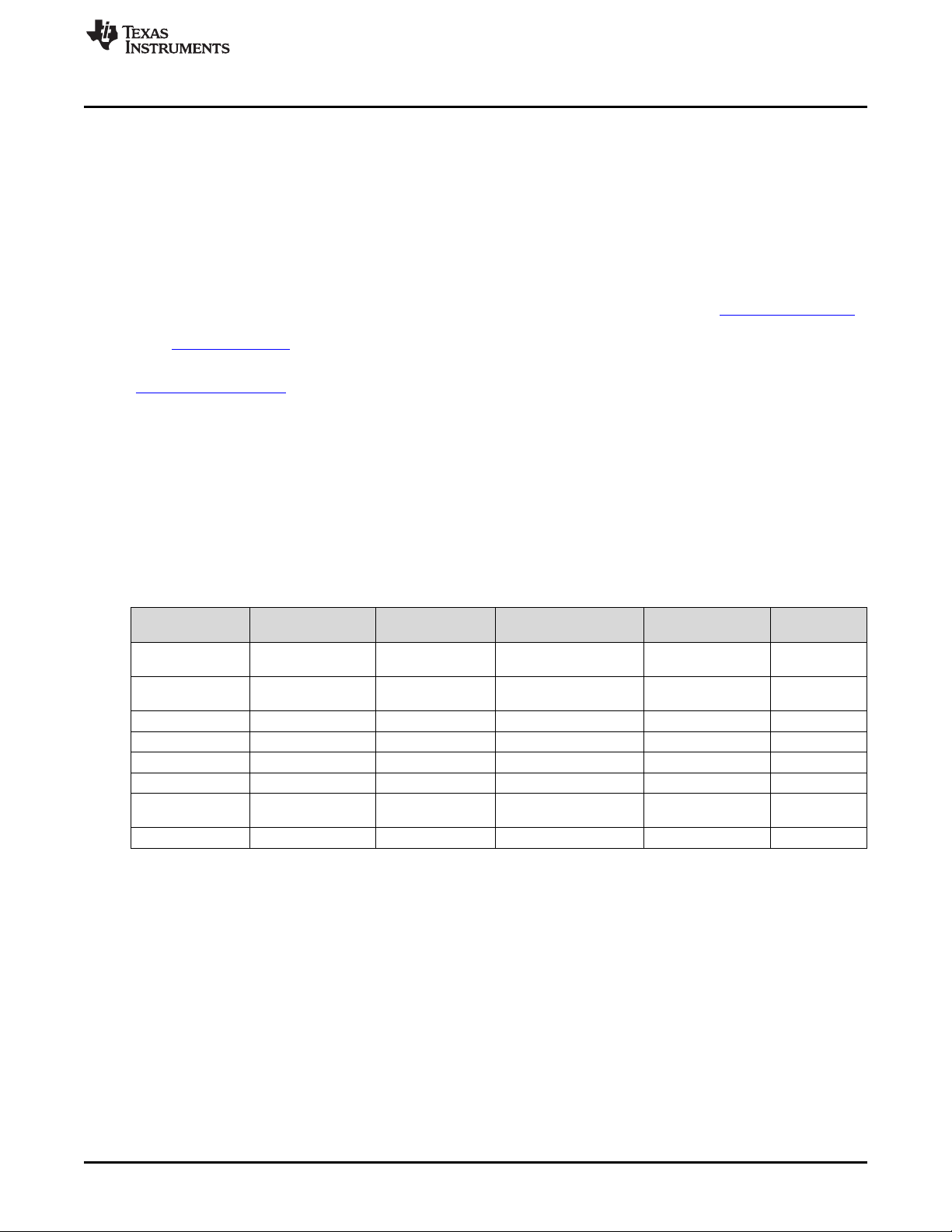
The CC253x System-on-Chip solution family consists of several devices. The following table provides a
device overview and points out the differences regarding memory sizes and peripherals. For a complete
feature list of any of the devices, see the corresponding data sheet (Appendix C).
FCC Warning
Table 0-1. CC253x Family Overview
Feature
FLASH_SIZE 128 KB, 256 KB 32 KB, 64 KB, 96 KB 128 KB, 256 KB
SRAM_SIZE 8 KB, 8 KB 4 KB, 4 KB, 6 KB 8 KB 8 KB
USB Not included Included Not included Included Not included
ADC Included Included Not included Included Included
Battery monitor Not included Not included Included Not included Not included
I2C Not included Not included Included Not included Included
Operational
amplifier
Analog comparator Included Included Not included Included Included
CC2530F32, -F64, CC2531F128, CC2533F32, CC2540F128, CC2541F128,
-F128/, -F256 CC2531F256 -F64, -F96 -F256 -F256
32 KB, 64 KB, 128 KB,
128 KB, 256 KB 256 KB
8 KB, 8 KB, 8 KB,
8 KB
Included Included Not included Included Not included
Legend:
FLASH_SIZE – The size of the flash
SRAM_SIZE – The size of the SRAM
SWRU191F–April 2009–Revised April 2014 Read This First
Submit Documentation Feedback
Copyright © 2009–2014, Texas Instruments Incorporated
15
Page 16

Register Conventions
Register Conventions
Each SFR and XREG register is described in a separate table, where each table title contains the
following information in the format indicated:
For SFR registers: REGISTER NAME (SFR address) – register description
For XREG registers: REGISTER NAME (XDATA address) – register description
Each table has five columns to describe the different register fields as described in the following:
Column 1 – Bit: Denotes which bits of the register are described and addressed in the specific row
Column 2 – Name: Specific name of the register field
Column 3 – Reset: Reset or initial value of the register field
Column 4 – R/W: Key indicating the accessibility of the bits in the field (see Table 0-2 for more details)
Column 5 – Description: More details about the register field, and often a description of the functions of
the different values
In the register descriptions, each register field is shown with a symbol (R/W) indicating the access mode of
the register field. The register values are always given in binary notation unless prefixed by 0x, which
indicates hexadecimal notation.
www.ti.com
Table 0-2. Register Bit Conventions
SYMBOL ACCESS MODE
R/W Read and write
R Read-only
R0 Read as 0
R1 Read as 1
W Write-only
W0 Write as 0
W1 Write as 1
H0 Hardware clear
H1 Hardware set
16
Read This First SWRU191F–April 2009–Revised April 2014
Copyright © 2009–2014, Texas Instruments Incorporated
Submit Documentation Feedback
Page 17

Chapter 1
SWRU191F–April 2009–Revised April 2014
Introduction
As mentioned in the preface, the CC253x, CC2540, and CC2541 device family provides solutions for a
wide range of applications. In order to help the user to develop these applications, this user's guide
focuses on the usage of the different building blocks of the CC253x, CC2540, and CC2541 device family.
For detailed device descriptions, complete feature lists, and performance numbers, see the device-specific
data sheet (Appendix C).
In order to provide easy access to relevant information, the following subsections guide the reader to the
different chapters in this guide.
Topic ........................................................................................................................... Page
1.1 Overview........................................................................................................... 18
1.2 Applications ...................................................................................................... 23
SWRU191F–April 2009–Revised April 2014 Introduction
Submit Documentation Feedback
Copyright © 2009–2014, Texas Instruments Incorporated
17
Page 18
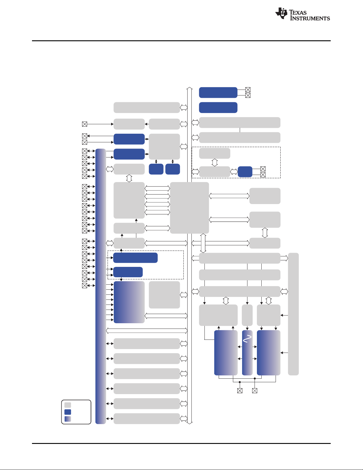
RESET
WATCHDOG
TIMER
IRQ CTRL
CC2530/CC2531
FLASH CTRL
DEBUG
INTERFACE
CLOCK MUX
and
CALIBRATION
DMA
8051 CPU
CORE
32-MHz
CRYSTAL OSC
32.768-kHz
CRYSTAL OSC
HIGH-
SPEED
RC-OSC
USART 0
USART 1
TIMER 1 (16-Bit)
TIMER 3 (8-Bit)
TIMER 4 (8-Bit)
TIMER 2
(IEEE 802.15.4 MAC TIMER)
32/64/128/256-KB
FLASH
8-KB SRAM
RESET_N
XOSC_Q2
XOSC_Q1
P2_4
P1_7
P0_7
P2_3
P1_6
P0_6
P2_2
P1_5
P0_5
P1_2
P0_2
P2_1
P1_4
P0_4
P1_1
P0_1
P2_0
P1_3
P0_3
P1_0
P0_0
MODULATOR
DEMODULATOR
AND AGC
RECEIVE TRANSMIT
FREQUENCY
SYNTHESIZER
SYNTH
RF_P RF_N
B0301-03
RADIO DATA INTERFACE
COMMAND STROBE PROCESSOR
RADIO REGISTERS
FIFO and FRAME CONTROL
SFR Bus
SFR Bus
12-BIT -
ADC
D S
AES
ENCRYPTION
AND
DECRYPTION
MEMORY
ARBITER
SFR
IRAM
XRAM
PDATA
32-kHz
RC-OSC
I/O CONTROLLER
DIGITAL
ANALOG
MIXED
POWER MANAGEMENT CONTROLLER
ON-CHIP VOLTAGE
REGULATOR
POWER-ON RESET
BROWNOUT
VDD (2 V–3.6 V)
DCOUPL
SLEEP TIMER
BATTERY MONITOR (CC2533 ONLY)
USB
USB
PHY
1-KB
FIFO SRAM
DP
DM
CC2531
OP-AMP
ANALOG COMPARATOR
Overview
1.1 Overview
The block diagrams in Figure 1-1, Figure 1-2, and Figure 1-3 show the different building blocks of the
CC253x and, CC2540, and CC2541 devices. Not all features and functions of all modules or peripherals
are present on all devices of the CC253x, CC2540, and CC2541; hence, see the device-specific data
sheet for a device-specific block diagram.
www.ti.com
18
Introduction SWRU191F–April 2009–Revised April 2014
Figure 1-1. CC253x Block Diagram
Copyright © 2009–2014, Texas Instruments Incorporated
Submit Documentation Feedback
Page 19
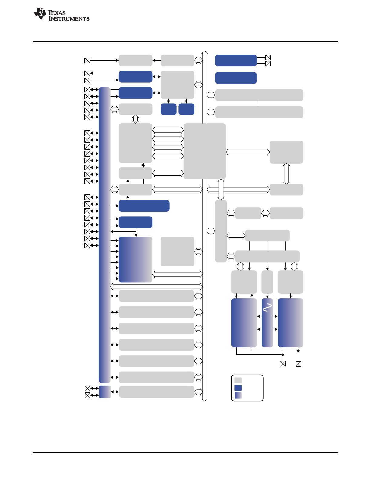
RESET
WATCHDOG
TIMER
IRQ CTRL
FLASH CTRL
DEBUG
INTERFACE
CLOCK MUX
and
CALIBRATION
DMA
8051 CPU
CORE
32-MHz
CRYSTAL OSC
OP-AMP
32.768-kHz
CRYSTAL OSC
HIGH-
SPEED
RC-OSC
POWER MANAGEMENT CONTROLLER
USART 0
USART 1
TIMER 1 (16-Bit)
TIMER 3 (8-Bit)
TIMER 4 (8-Bit)
TIMER 2
(BLE LL TIMER)
FLASH
FIFOCTRL
1 KB SRAM
ON-CHIP VOLTAGE
REGULATOR
POWER-ON RESET
BROWN OUT
VDD (2 V–3.6 V)
DCOUPL
RESET_N
XOSC_Q2
XOSC_Q1
P2_4
P1_7
P0_7
P2_3
P1_6
P0_6
P2_2
P1_5
P0_5
P1_2
P0_2
P2_1
P1_4
P0_4
P1_1
P0_1
P2_0
P1_3
P0_3
P1_0
P0_0
MODULATOR
DEMODULATOR
RECEIVE
TRANSMIT
FREQUENCY
SYNTHESIZER
SYNTH
RF_P
RF_N
B0301a-055
RADIO REGISTERS
SFR Bus
SFR Bus
DS
ADC
AUDIO/DC
AES
ENCRYPTION
AND
DECRYPTION
MEMORY
ARBITRATOR
FLASH
UNIFIED
SFR
IRAM
XRAM
PDATA
SLEEP TIMER
32-kHz
RC-OSC
I/O CONTROLLER
DIGITAL
ANALOG
MIXED
ANALOG COMPARATOR
Radio Arbiter
Link Layer Engine
USB
USB_N
USB_P
USB
PHY
www.ti.com
Overview
The modules can be roughly divided into one of three categories: CPU and memory related modules;
Figure 1-2. CC2540 Block Diagram
modules related to peripherals, clocks, and power management; and radio-related modules.
SWRU191F–April 2009–Revised April 2014 Introduction
Submit Documentation Feedback
Copyright © 2009–2014, Texas Instruments Incorporated
19
Page 20
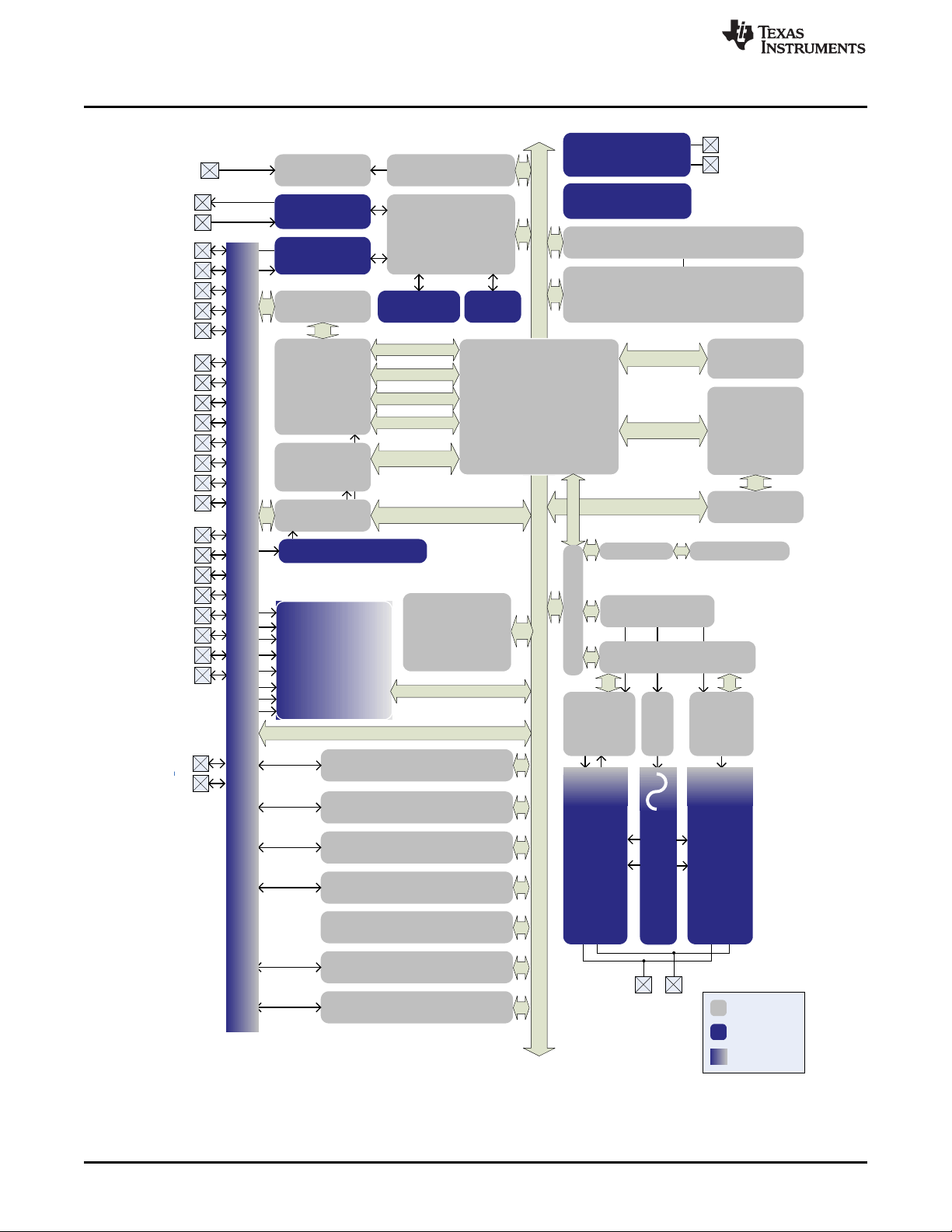
SFR bus SFR bus
MEMORY
ARBITRATOR
8051 CPU
CORE
DMA
FLASH
SRAM
FLASH CTRL
DEBUG
INTERFACE
RESET
RESET_N
P2_4
P2_3
P2_2
P2_1
P2_0
P1_4
P1_3
P1_2
P1_1
P1_0
P1_7
P1_6
P1_5
P0_4
P0_3
P0_2
P0_1
P0_0
P0_7
P0_6
P0_5
32.768-kHz
CRYSTAL OSC
32-MHZ
CRYSTAL OSC
HIGH SPEED
RC-OSC
32-kHz
RC-OSC
CLOCK MUX and
CALIBRATION
RAM
USART 0
USART 1
TIMER 1 (16-Bit)
TIMER 3 (8-bit)
TIMER 2
(BLE LL TIMER)
TIMER 4 (8-bit)
AES
ENCRYPTION
and
DECRYPTION
WATCHDOG TIMER
IRQ
CTRL
FLASH
UNIFIED
RF_P RF_N
SYNTH
MODULATOR
POWER-ON RESET
BROWN OUT
RADIO
REGISTERS
POWER MGT. CONTROLLER
SLEEP TIMER
PDATA
XRAM
IRAM
SFR
XOSC_Q2
XOSC_Q1
DS ADC
AUDIO / DC
DIGITAL
ANALOG
MIXED
VDD (2 V–3.6 V)
DCOUPL
ON-CHIP VOLTAGE
REGULATOR
Link Layer Engine
FREQUENCY
SYNTHESIZER
I2C
DEMODULATOR
RECEIVE TRANSMIT
OP-
ANALOG COMPARATOR
I/O CONTROLLER
1-KB SRAM
Radio Arbiter
FIFOCTRL
SDA
SCL
Overview
www.ti.com
20
Submit Documentation Feedback
Introduction SWRU191F–April 2009–Revised April 2014
Figure 1-3. CC2541 Block Diagram
Copyright © 2009–2014, Texas Instruments Incorporated
Page 21

www.ti.com
1.1.1 CPU and Memory
The 8051 CPU core is a single-cycle 8051-compatible core. It has three different memory access buses
(SFR, DATA, and CODE/XDATA) with single-cycle access to SFR, DATA, and the main SRAM. It also
includes a debug interface and an 18-input extended interrupt unit. The detailed functionality of the CPU
and the memory is addressed in Chapter 2.
The interrupt controller services a total of 18 interrupt sources, divided into six interrupt groups, each of
which is associated with one of four interrupt priorities. Any interrupt service request is serviced also when
the device is in idle mode by going back to active mode. Some interrupts can also wake up the device
from sleep mode (when in sleep mode, the device is in one of the three low-power modes PM1, PM2, or
PM3); see Chapter 4 for more details.
The memory arbiter is at the heart of the system, as it connects the CPU and DMA controller with the
physical memories and all peripherals through the SFR bus. The memory arbiter has four memory access
points, access of which can map to one of three physical memories: SRAM, flash memory, and
XREG/SFR registers. The memory arbiter is responsible for performing arbitration and sequencing
between simultaneous memory accesses to the same physical memory.
The 4-, 6-, or 8-KB SRAM maps to the DATA memory space and to parts of the XDATA memory spaces.
The SRAM is an ultralow-power SRAM that retains its contents in all power modes. This is an important
feature for low-power applications.
The 32-, 64-, 96-, 128-, or 256-KB flash block provides in-circuit programmable non-volatile program
memory for the device, and maps into the CODE and XDATA memory spaces. In addition to holding
program code and constants, the non-volatile memory allows the application to save data that must be
preserved such that it is available after restarting the device. Using this feature one can, for example, use
saved network-specific data to avoid the need for a full start-up and network find-and-join process.
Overview
1.1.2 Clocks and Power Management
The digital core and peripherals are powered by a 1.8-V low-dropout voltage regulator (Chapter 26).
Additionally, the CC253x, CC2540, and CC2541 contain a power-management functionality that allows the
use of different low-power modes (PM1, PM2, and PM3) for low-power applications with a long battery life
(see Chapter 4 for more details). Five different reset sources exist to reset the device; see Chapter 5 for
more details.
1.1.3 Peripherals
The CC253x, CC2540, and CC2541 include many different peripherals that allow the application designer
to develop advanced applications. Not all peripherals are present on all devices. See Table 0-1 for a listing
of which peripherals are present on each device.
The debug interface (Chapter 3) implements a proprietary two-wire serial interface that is used for incircuit debugging. Through this debug interface, it is possible to perform an erasure of the entire flash
memory, control which oscillators are enabled, stop and start execution of the user program, execute
supplied instructions on the 8051 core, set code breakpoints, and single-step through instructions in the
code. Using these techniques, it is possible to perform in-circuit debugging and external flash
programming elegantly.
The device contains flash memory for storage of program code. The flash memory is programmable from
the user software and through the debug interface (as mentioned previously). The flash controller
(Chapter 6) handles writing and erasing the embedded flash memory. The flash controller allows pagewise erasure and 4-bytewise programming.
The I/O controller (Chapter 7) is responsible for all general-purpose I/O pins. The CPU can configure
whether peripheral modules control certain pins or whether they are under software control, and if so,
whether each pin is configured as an input or output and if a pullup or pulldown resistor in the pad is
connected. CPU interrupts can be enabled on each pin individually. Each peripheral that connects to the
I/O pins can choose between two different I/O pin locations to ensure flexibility in various applications.
SWRU191F–April 2009–Revised April 2014 Introduction
Submit Documentation Feedback
Copyright © 2009–2014, Texas Instruments Incorporated
21
Page 22

Overview
www.ti.com
A versatile five-channel DMA controller (Chapter 8) is available in the system, accesses memory using
the XDATA memory space, and thus has access to all physical memories. Each channel (trigger, priority,
transfer mode, addressing mode, source and destination pointers, and transfer count) is configured with
DMA descriptors anywhere in memory. Many of the hardware peripherals (AES core, flash controller,
USARTs, timers, ADC interface) achieve highly efficient operation by using the DMA controller for data
transfers between SFR or XREG addresses and flash or SRAM.
Timer 1 (Chapter 9) is a 16-bit timer with timer, counter, and PWM functionality. Timer 1 has a
programmable prescaler, a 16-bit period value, and five individually programmable counter or capture
channels, each with a 16-bit compare value. Each of the counter or capture channels can be used as a
PWM output or to capture the timing of edges on input signals. Timer 1 can also be configured in IR
generation mode, where it counts Timer 3 periods and the output is ANDed with the output of Timer 3 to
generate modulated consumer IR signals with minimal CPU interaction (see Section 9.9).
Timer 2 (MAC Timer) (Chapter 22) is specially designed for supporting an IEEE 802.15.4 MAC or other
time-slotted protocol in software. The timer has a configurable timer period and a 24-bit overflow counter
that can be used to keep track of the number of periods that have transpired. A 40-bit capture register is
also used to record the exact time at which a start-of-frame delimiter is received or transmitted, or the
exact time at which transmission ends, as well as two 16-bit output compare registers and two 24-bit
overflow compare registers that can send various command strobes (start RX, start TX, etc.) at specific
times to the radio modules.
Timer 3 and Timer 4 (Chapter 10) are 8-bit timers with timer, counter, and PWM functionality. They have
a programmable prescaler, an 8-bit period value, and one programmable counter channel with an 8-bit
compare value. Each of the counter channels can be used as a PWM output.
The Sleep Timer (Chapter 11) is an ultralow-power timer that counts 32-kHz crystal oscillator or 32-kHz
RC oscillator periods. The Sleep Timer runs continuously in all operating modes except power mode 3
(PM3). Typical applications of this timer are as a real-time counter or as a wake-up timer for coming out of
power mode 1 (PM1) or power mode 2 (PM2).
The ADC (Chapter 12) supports 7 bits (30-kHz bandwidth) to 12 bits (4-kHz bandwidth) of resolution. DC
and audio conversions with up to eight input channels (Port 0) are possible. The inputs can be selected as
single-ended or differential. The reference voltage can be internal, AVDD, or a single-ended or differential
external signal. The ADC also has a temperature-sensor input channel. The ADC can automate the
process of periodic sampling or conversion over a sequence of channels.
The battery monitor (Chapter 13) (CC2533 only) enables simple voltage monitoring in devices that do
not include an ADC. It is designed such that it is accurate in the voltage areas around 2 V, with lower
resolution at higher voltages.
The random-number generator (Chapter 14) uses a 16-bit LFSR to generate pseudorandom numbers,
which can be read by the CPU or used directly by the command strobe processor. The random-number
generator can be seeded with random data from noise in the radio ADC.
The AES coprocessor (Chapter 15) allows the user to encrypt and decrypt data using the AES algorithm
with 128-bit keys. The core is able to support the security operations required by IEEE 802.15.4 MAC
security, the ZigBee network layer, and the application layer.
A built-in Watchdog Timer (Chapter 16) allows the device to reset itself in case the firmware hangs.
When enabled by software, the Watchdog Timer must be cleared periodically; otherwise, it resets the
device when it times out. It can alternatively be configured for use as a general 32-kHz timer.
USART 0 and USART 1 (Chapter 18) are each configurable as either a SPI master or slave or as a
UART. They provide double buffering on both RX and TX and hardware flow control, and are thus well
suited to high-throughput full-duplex applications. Each has its own high-precision baud-rate generator,
thus leaving the ordinary timers free for other uses.
The I2C module (Chapter 20) (CC2533 and CC2541) provides a digital peripheral connection with two pins
and supports both master and slave operation.
The USB 2.0 controller (Chapter 21) (CC2531 and CC2540) operates at Full-Speed, 12 Mbps transfer
rate. The controller has five bidirectional endpoints in addition to control endpoint 0. The endpoints support
bulk, Interrupt, and Isochronous operation for implementation of a wide range of applications. The 1024
bytes of dedicated, flexible FIFO memory combined with DMA access ensures that a minimum of CPU
involvement is needed for USB communication.
22
Introduction SWRU191F–April 2009–Revised April 2014
Copyright © 2009–2014, Texas Instruments Incorporated
Submit Documentation Feedback
Page 23

www.ti.com
The operational amplifier (Chapter 18) (CC2530, CC2531, and CC2540) is intended to provide front-end
buffering and gain for the ADC. Both the inputs as well as the output are available on pins, so the
feedback network is fully customizable. A chopper-stabilized mode is available for applications that need
good accuracy with high gain.
The ultralow-power analog comparator (Chapter 19) (CC2530, CC2531, CC2540, and CC2541) enables
applications to wake up from PM2 or PM3 based on an analog signal. Both inputs are brought out to pins;
the reference voltage must be provided externally. The comparator output is mapped into the digital I/O
port and can be treated by the MCU as a regular digital input.
1.1.4 Radio
The CC2540 and CC2541 provide a Bluetooth low energy-compliant radio transceiver. The RF core which
controls the analog and digital radio modules is only indirectly accessible through API commands to the
BLE stack. More details about the CC2540 or CC2541 BLE radio can be found in Chapter 24. The
CC2541 can also be run in proprietary modes; more details can be found in Chapter 25.
The CC253x device family provides an IEEE 802.15.4-compliant radio transceiver. The RF core
controls the analog radio modules. In addition, it provides an interface between the MCU and the radio
which makes it possible to issue commands, read status, and automate and sequence radio events. The
radio also includes a packet-filtering and address-recognition module. More details about the CC253x
radio can be found in Chapter 23.
1.2 Applications
As shown in the overview (Section 1.1), this user's guide focuses on the functionality of the different
modules that are available to build different types of applications based on the CC253x,CC2540, and
CC2541 device family. When looking at the complete application development process, additional
information is useful. However, as this information and help is not device-specific (that is, not unique for
the CC253x, CC2540, and 41 device family), see the additional information sources in the following
paragraphs.
The first step is to set up the development environment (hardware, tools, and so forth) by purchasing a
development kit (see the device-specific product Web site to find links to the relevant development kits).
The development kits come with an out-of-the-box demonstration and information on how to set up the
development environment; install required drivers (done easily by installing the SmartRF software,
Section 27.1), set up the compiler tool chain, and so forth. As soon as one has installed the development
environment, one is ready to start the application development.
The easiest way to write the application software is to base the application on one of the available
standard protocols (RemoTI network protocol, Section 27.2; TIMAC software, Section 27.4; Z-Stack
software for ZigBee-compliant solutions, Section 27.5); BLE stack software for Bluetooth low energycompliant solutions Section 27.6; or the proprietary SimpliciTI network protocol, Section 27.3. They all
come with several sample applications.
For the hardware layout design of the user-specific hardware, the designer can find reference designs on
the different product pages (Section B.1). By copying these designs, the designer achieves optimal
performance. The developed hardware can then be tested easily using the SmartRF Studio software
(Section 27.1).
In case the final system should not have the expected performance, it is recommended to try out the
developed software on the development kit hardware and see how it works there. To check the userspecific hardware, it is a good first step to use SmartRF Studio software to compare the development kit
performance versus the user-specific hardware using the same settings.
The user can also find additional information and help by joining the Low-Power RF Online Community
(Section B.2) and by subscribing to the Low-Power RF eNewsletter (Section B.4).
To contact a third-party to help with development or to use modules, check out the Texas Instruments
Low-Power RF Developer Network (Section B.3).
Overview
SWRU191F–April 2009–Revised April 2014 Introduction
Submit Documentation Feedback
Copyright © 2009–2014, Texas Instruments Incorporated
23
Page 24

Chapter 2
SWRU191F–April 2009–Revised April 2014
8051 CPU
The System-on-Chip solution is based on an enhanced 8051 core. More details regarding the core,
memory map, instruction set, and interrupts are described in the following subsections.
Topic ........................................................................................................................... Page
2.1 8051 CPU Introduction........................................................................................ 25
2.2 Memory............................................................................................................. 25
2.3 CPU Registers ................................................................................................... 34
2.4 Instruction Set Summary..................................................................................... 36
2.5 Interrupts .......................................................................................................... 40
24
8051 CPU SWRU191F–April 2009–Revised April 2014
Copyright © 2009–2014, Texas Instruments Incorporated
Submit Documentation Feedback
Page 25

www.ti.com
2.1 8051 CPU Introduction
The enhanced 8051 core uses the standard 8051 instruction set. Instructions execute faster than the
standard 8051 due to the following:
• One clock per instruction cycle is used as opposed to 12 clocks per instruction cycle in the standard
8051.
• Wasted bus states are eliminated.
Because an instruction cycle is aligned with memory fetch when possible, most of the single-byte
instructions are performed in a single clock cycle. In addition to the speed improvement, the enhanced
8051 core also includes architectural enhancements:
• A second data pointer
• An extended 18-source interrupt unit
The 8051 core is object-code-compatible with the industry-standard 8051 microcontroller. That is, object
code compiled with an industry-standard 8051 compiler or assembler executes on the 8051 core and is
functionally equivalent. However, because the 8051 core uses a different instruction timing than many
other 8051 variants, existing code with timing loops may require modification. Also, because the peripheral
units such as timers and serial ports differ from those on other 8051 cores, code which includes
instructions using the peripheral-unit SFRs does not work correctly.
Flash prefetching is not enabled by default, but improves CPU performance by up to 33%. This is at the
expense of slightly increased power consumption, but in most cases improves energy consumption as it is
faster. Flash prefetching can be enabled in the FCTL register.
8051 CPU Introduction
2.2 Memory
The 8051 CPU architecture has four different memory spaces. The 8051 has separate memory spaces for
program memory and data memory. The 8051 memory spaces are the following (see Section 2.2.1 and
Section 2.2.2 for details):
CODE. A read-only memory space for program memory. This memory space addresses 64 KB.
DATA. A read-or-write data memory space that can be directly or indirectly accessed by a single-cycle
CPU instruction. This memory space addresses 256 bytes. The lower 128 bytes of the DATA memory
space can be addressed either directly or indirectly, the upper 128 bytes only indirectly.
XDATA. A read-and-write data memory space, access to which usually requires 4–5 CPU instruction
cycles. This memory space addresses 64 KB. Access to XDATA memory is also slower than DATA
access, as the CODE and XDATA memory spaces share a common bus on the CPU core, and instruction
prefetch from CODE thus cannot be performed in parallel with XDATA accesses.
SFR. A read-or-write register memory space which can be directly accessed by a single CPU instruction.
This memory space consists of 128 bytes. For SFR registers whose address is divisible by eight, each bit
is also individually addressable.
The four different memory spaces are distinct in the 8051 architecture, but are partly overlapping in the
device to ease DMA transfers and hardware debugger operation.
How the different memory spaces are mapped onto the three physical memories (flash program memory,
SRAM, and memory-mapped registers) is described in Section 2.2.1 and Section 2.2.2.
2.2.1 Memory Map
The memory map differs from the standard 8051 memory map in two important aspects, as described in
the following paragraphs.
First, in order to allow the DMA controller access to all physical memory and thus allow DMA transfers
between the different 8051 memory spaces, parts of SFR and the DATA memory space are mapped into
the XDATA memory space (see Figure 2-1).
Second, two alternative schemes for CODE memory space mapping can be used. The first scheme is the
standard 8051 mapping where only the program memory (that is, flash memory) is mapped to CODE
memory space. This mapping is the default after a device reset and is shown in Figure 2-2.
SWRU191F–April 2009–Revised April 2014 8051 CPU
Submit Documentation Feedback
Copyright © 2009–2014, Texas Instruments Incorporated
25
Page 26
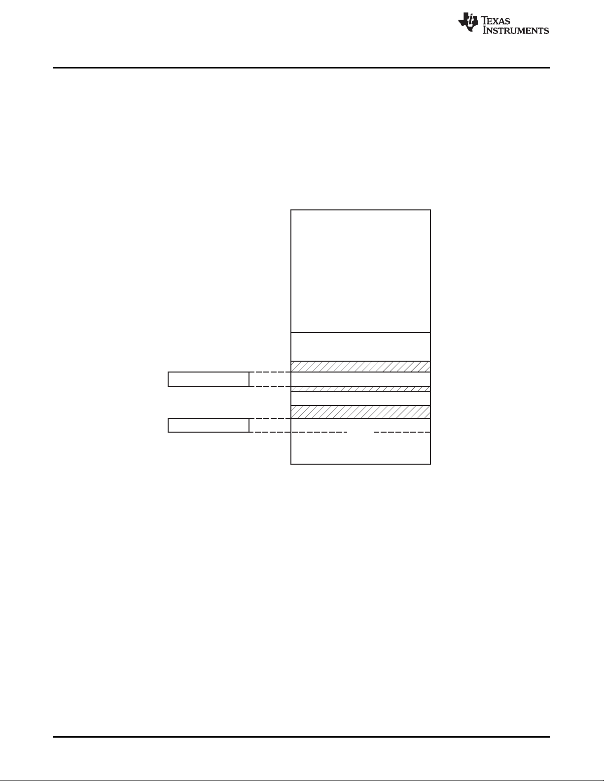
0 xFFFF
0x8000
0x0000
0x 6000
XREG(1KB)
0x63FF
SFR(128B)
0x 7080
SRAM_SIZE – 1
SRAMSIZE – 256
0x7 FFF
XBANK
(SELECTABLE32KBFLASHBANK)
8051SFRSPACE
8051DATA SPACE
INFORMATIONPAGE
(2KB)
0x70FF
0x 7800
M0097-02
SRAM
(SRAM_SIZEBytes)
Memory
www.ti.com
The second scheme is used for executing code from SRAM. In this mode, the SRAM is mapped into the
region of 0x8000 through (0x8000 + SRAM_SIZE – 1). The map is shown in Figure 2-3. Executing code
from SRAM improves performance and reduces power consumption.
The upper 32 KB of XDATA is a read-only area called XBANK (see Figure 2-1). Any of the available 32
KB flash banks can be mapped in here. This gives software access to the whole flash memory. This area
is typically used to store additional constant data.
Details about mapping of all 8051 memory spaces are given in Section 2.2.2.
The memory map showing how the different physical memories are mapped into the CPU memory spaces
is given in Figure 2-1 through Figure 2-3. The number of available flash banks depends on the flash size
option.
26
Figure 2-1. XDATA Memory Space (Showing SFR and DATA Mapping)
8051 CPU SWRU191F–April 2009–Revised April 2014
Copyright © 2009–2014, Texas Instruments Incorporated
Submit Documentation Feedback
Page 27

0x 0000
0x7FFF
0x 8000
0 xFFFF
Bank0–7
(32KBFLASH)
Common Area/Bank0
(32KBFLASH)
M0098-02
0x 0000
0x7FFF
0x 8000
0 xFFFF
SRAM
0x8000 + SRAM_SIZE – 1
0x8000 + SRAM_SIZE
Banks 0–7
(Upper 24KB FLASH)
Common Area/Bank 0
(32KB FLASH)
M0099-04
www.ti.com
2.2.2 CPU Memory Space
Memory
Figure 2-2. CODE Memory Space Figure 2-3. CODE Memory Space for Running Code
From SRAM
XDATA memory space. The XDATA memory map is given in Figure 2-1.
The SRAM is mapped into address range of 0x0000 through (SRAM_SIZE – 1).
The XREG area is mapped into the 1 KB address range (0x6000–0x63FF). These registers are additional
registers, effectively extending the SFR register space. Some peripheral registers and most of the radio
control and data registers are mapped in here.
The SFR registers are mapped into address range (0x7080–0x70FF).
The flash information page (2 KB) is mapped into the address range (0x7800–0x7FFF). This is a read-only
area and contains various information about the device.
The upper 32 KB of the XDATA memory space (0x8000–0xFFFF) is a read-only flash code bank (XBANK)
and can be mapped to any of the available flash banks using the MEMCTR.XBANK[2:0] bits.
The mapping of flash memory, SRAM, and registers to XDATA allows the DMA controller and the CPU
access to all the physical memories in a single unified address space.
Writing to unimplemented areas in the memory map (shaded in the figure) has no effect. Reading from
unimplemented areas returns 0x00. Writes to read-only regions, that is, flash areas, are ignored.
CODE memory space. The CODE memory space is 64 KB and is divided into a common area
(0x0000–0x7FFF) and a bank area (0x8000–0xFFFF) as shown in Figure 2-2. The common area is
always mapped to the lower 32 KB of the physical flash memory (bank 0). The bank area can be mapped
to any of the available 32-KB flash banks (from 0 to 7). The number of available flash banks depends on
the flash size option. Use the flash-bank-select register, FMAP, to select the flash bank. On 32-KB
devices, no flash memory can be mapped into the bank area. Reads from this region return 0x00 on these
devices.
To allow program execution from SRAM, it is possible to map the available SRAM into the lower range of
the bank area from 0x8000 through (0x8000 + SRAM_SIZE – 1). The rest of of the currently selected bank
is still mapped into the address range from (0x8000 + SRAM_SIZE) through 0xFFFF). Set the
MEMCTR.XMAP bit to enable this feature.
DATA memory space. The 8-bit address range of DATA memory is mapped into the upper 256 bytes of
the SRAM, that is, the address range from (SRAM_SIZE – 256) through (SRAM_SIZE – 1).
SWRU191F–April 2009–Revised April 2014 8051 CPU
Submit Documentation Feedback
Copyright © 2009–2014, Texas Instruments Incorporated
27
Page 28

Memory
SFR memory space. The 128-entry hardware register area is accessed through this memory space. The
SFR registers are also accessible through the XDATA address space at the address range
(0x7080–0x70FF). Some CPU-specific SFR registers reside inside the CPU core and can only be
accessed using the SFR memory space and not through the duplicate mapping into XDATA memory
space. These specific SFR registers are listed in SFR Registers.
2.2.3 Physical Memory
RAM. All devices contain static RAM. At power on, the content of RAM is undefined. RAM content is
retained in all power modes.
Flash Memory. The on-chip flash memory is primarily intended to hold program code and constant data.
The flash memory has the following features:
• Page size: 1 KB or 2 KB (details are given in the data sheet of the device.)
• Flash-page erase time: 20 ms
• Flash-chip (mass) erase time: 20 ms
• Flash write time (4 bytes): 20 μs
• Data retention (at room temperature): 100 years
• Program and erase endurance: 20,000 cycles
The flash memory is organized as a set of 1 or 2 KB pages. The 16 bytes of the upper available page
contain page-lock bits and the debug-lock bit. There is one lock bit for each page, except the lock-bit page
which is implicitly locked when not in debug mode. When the lock bit for a page is 0, it is impossible to
erase or write that page. When the debug lock bit is 0, most of the commands on the debug interface are
ignored. The primary purpose of the debug lock bit is to protect the contents of the flash against read-out.
The Flash Controller is used to write and erase the contents of the flash memory.
When the CPU reads instructions and constants from flash memory, it fetches the instructions through a
cache. Four bytes of instructions and four bytes of constant data are cached, at 4-byte boundaries. That
is, when the CPU reads from address 0x00F1 for example, bytes 0x00F0–0x00F3 are cached. A separate
prefetch unit is capable of prefetching 4 additional bytes of instructions. The cache is provided mainly to
reduce power consumption by reducing the amount of time the flash memory is accessed. The cache may
be disabled with the FCTL.CM[1:0] register bits. Doing so increases power consuption and is not
recommended. The execution time from flash is not cycle-accurate when using the default cache mode
and the cache mode with prefetch; that is, one cannot determine exactly the number of clock cycles a set
of instructions takes. To obtain cycle-accurate execution, enable the real-time cache mode and ensure all
DMA transfers have low priority. The prefetch mode improves performance by up to 33%, at the expense
of increased power consumption due to wasted flash reads. Typically, performance improves by
15%–20%. Total energy, however, may decrease (depending on the application) due to fewer wasted
clock cycles waiting for the flash to return instructions and/or data. Prefetching is very applicationdependent and requires the use of power modes to be effective.
The Information Page is a 2 KB read-only region that stores various device information. Among other
things, it contains for IEEE 802.15.4 or Bluetooth low energy compliant devices a unique IEEE address
from the TI range of addresses. For CC253x, this is a 64-bit IEEE address stored with least-significant
byte first at XDATA address 0x780C. For CC2540 and CC2541, this is a 48-bit IEEE address stored with
least-significant byte first at XDATA address 0x780E.
SFR Registers. The special function registers (SFRs) control several of the features of the 8051 CPU
core and/or peripherals. Many of the 8051 core SFRs are identical to the standard 8051 SFRs. However,
there are additional SFRs that control features that are not available in the standard 8051. The additional
SFRs are used to interface with the peripheral units and RF transceiver.
Table 2-1 shows the addresses of all SFRs in the device. The 8051 internal SFRs are shown with gray
background, whereas the other SFRs are the SFRs specific to the device.
www.ti.com
28
NOTE: All internal SFRs (shown with gray background in Table 2-1), can only be accessed through
SFR space, as these registers are not mapped into XDATA space. One exception is the port
registers (P0, P1, and P2) which are readable from XDATA.
8051 CPU SWRU191F–April 2009–Revised April 2014
Copyright © 2009–2014, Texas Instruments Incorporated
Submit Documentation Feedback
Page 29
www.ti.com
Memory
Table 2-1. SFR Overview
Register SFR
Name Address
ADCCON1 0xB4 ADC ADC control 1
ADCCON2 0xB5 ADC ADC control 2
ADCCON3 0xB6 ADC ADC control 3
ADCL 0xBA ADC ADC data low
ADCH 0xBB ADC ADC data high
RNDL 0xBC ADC Random number generator data low
RNDH 0xBD ADC Random number generator data high
ENCDI 0xB1 AES Encryption or decryption input data
ENCDO 0xB2 AES Encryption or decryption output data
ENCCS 0xB3 AES Encryption or decryption control and status
P0 0x80 CPU Port 0. Readable from XDATA (0x7080)
SP 0x81 CPU Stack pointer
DPL0 0x82 CPU Data pointer 0 low byte
DPH0 0x83 CPU Data pointer 0 high byte
DPL1 0x84 CPU Data pointer 1 low byte
DPH1 0x85 CPU Data pointer 0 high byte
PCON 0x87 CPU Power mode control
TCON 0x88 CPU Interrupt flags
P1 0x90 CPU Port 1. Readable from XDATA (0x7090)
DPS 0x92 CPU Data pointer select
S0CON 0x98 CPU Interrupt flags 2
IEN2 0x9A CPU Interrupt enable 2
S1CON 0x9B CPU Interrupt flags 3
P2 0xA0 CPU Port 2. Readable from XDATA (0x70A0)
IEN0 0xA8 CPU Interrupt enable 0
IP0 0xA9 CPU Interrupt priority 0
IEN1 0xB8 CPU Interrupt enable 1
IP1 0xB9 CPU Interrupt priority 1
IRCON 0xC0 CPU Interrupt flags 4
PSW 0xD0 CPU Program status Word
ACC 0xE0 CPU Accumulator
IRCON2 0xE8 CPU Interrupt flags 5
B 0xF0 CPU B register
DMAIRQ 0xD1 DMA DMA interrupt flag
DMA1CFGL 0xD2 DMA DMA channel 1–4 configuration address low
DMA1CFGH 0xD3 DMA DMA channel 1–4 configuration address high
DMA0CFGL 0xD4 DMA DMA channel 0 configuration address low
DMA0CFGH 0xD5 DMA DMA channel 0 configuration address high
DMAARM 0xD6 DMA DMA channel armed
DMAREQ 0xD7 DMA DMA channel start request and status
— 0xAA — Reserved
— 0x8E — Reserved
— 0x99 — Reserved
— 0xB0 — Reserved
— 0xB7 — Reserved
— 0xC8 — Reserved
P0IFG 0x89 IOC Port 0 interrupt status flag
Module Description
SWRU191F–April 2009–Revised April 2014 8051 CPU
Submit Documentation Feedback
Copyright © 2009–2014, Texas Instruments Incorporated
29
Page 30

Memory
Table 2-1. SFR Overview (continued)
Register SFR
Name Address
P1IFG 0x8A IOC Port 1 interrupt status flag
P2IFG 0x8B IOC Port 2 interrupt status flag
PICTL 0x8C IOC Port pins interrupt mask and edge
P0IEN 0xAB IOC Port 0 interrupt mask
P1IEN 0x8D IOC Port 1 interrupt mask
P2IEN 0xAC IOC Port 2 interrupt mask
P0INP 0x8F IOC Port 0 input mode
PERCFG 0xF1 IOC Peripheral I/O control
APCFG 0xF2 IOC Analog peripheral I/O configuration
P0SEL 0xF3 IOC Port 0 function select
P1SEL 0xF4 IOC Port 1 function select
P2SEL 0xF5 IOC Port 2 function select
P1INP 0xF6 IOC Port 1 input mode
P2INP 0xF7 IOC Port 2 input mode
P0DIR 0xFD IOC Port 0 direction
P1DIR 0xFE IOC Port 1 direction
P2DIR 0xFF IOC Port 2 direction
PMUX 0xAE IOC Power-down signal mux
MPAGE 0x93 MEMORY Memory page select
MEMCTR 0xC7 MEMORY Memory system control
FMAP 0x9F MEMORY Flash-memory bank mapping
RFIRQF1 0x91 RF RF interrupt flags MSB
RFD 0xD9 RF RF data
RFST 0xE1 RF RF command strobe
RFIRQF0 0xE9 RF RF interrupt flags LSB
RFERRF 0xBF RF RF error interrupt flags
ST0 0x95 ST Sleep Timer 0
ST1 0x96 ST Sleep Timer 1
ST2 0x97 ST Sleep Timer 2
STLOAD 0xAD ST Sleep-timer load status
SLEEPCMD 0xBE PMC Sleep-mode control command
SLEEPSTA 0x9D PMC Sleep-mode control status
CLKCONCMD 0xC6 PMC Clock control command
CLKCONSTA 0x9E PMC Clock control status
T1CC0L 0xDA Timer 1 Timer 1 channel 0 capture or compare value low
T1CC0H 0xDB Timer 1 Timer 1 channel 0 capture or compare value high
T1CC1L 0xDC Timer 1 Timer 1 channel 1 capture or compare value low
T1CC1H 0xDD Timer 1 Timer 1 channel 1 capture or compare value high
T1CC2L 0xDE Timer 1 Timer 1 channel 2 capture or compare value low
T1CC2H 0xDF Timer 1 Timer 1 channel 2 capture or compare value high
T1CNTL 0xE2 Timer 1 Timer 1 counter low
T1CNTH 0xE3 Timer 1 Timer 1 counter high
T1CTL 0xE4 Timer 1 Timer 1 control and status
T1CCTL0 0xE5 Timer 1 Timer 1 channel 0 capture or compare control
T1CCTL1 0xE6 Timer 1 Timer 1 channel 1 capture or compare control
T1CCTL2 0xE7 Timer 1 Timer 1 channel 2 capture or compare control
T1STAT 0xAF Timer 1 Timer 1 status
Module Description
www.ti.com
30
8051 CPU SWRU191F–April 2009–Revised April 2014
Copyright © 2009–2014, Texas Instruments Incorporated
Submit Documentation Feedback
Page 31

www.ti.com
Table 2-1. SFR Overview (continued)
Register SFR
Name Address
T2CTRL 0x94 Timer 2 Timer 2 control
T2EVTCFG 0x9C Timer 2 Timer 2 event configuration
T2IRQF 0xA1 Timer 2 Timer 2 interrupt flags
T2M0 0xA2 Timer 2 Timer 2 multiplexed register 0
T2M1 0xA3 Timer 2 Timer 2 multiplexed register 1
T2MOVF0 0xA4 Timer 2 Timer 2 multiplexed overflow register 0
T2MOVF1 0xA5 Timer 2 Timer 2 multiplexed overflow register 1
T2MOVF2 0xA6 Timer 2 Timer 2 multiplexed overflow register 2
T2IRQM 0xA7 Timer 2 Timer 2 interrupt mask
T2MSEL 0xC3 Timer 2 Timer 2 multiplex select
T3CNT 0xCA Timer 3 Timer 3 counter
T3CTL 0xCB Timer 3 Timer 3 control
T3CCTL0 0xCC Timer 3 Timer 3 channel 0 compare control
T3CC0 0xCD Timer 3 Timer 3 channel 0 compare value
T3CCTL1 0xCE Timer 3 Timer 3 channel 1 compare control
T3CC1 0xCF Timer 3 Timer 3 channel 1 compare value
T4CNT 0xEA Timer 4 Timer 4 counter
T4CTL 0xEB Timer 4 Timer 4 control
T4CCTL0 0xEC Timer 4 Timer 4 channel 0 compare control
T4CC0 0xED Timer 4 Timer 4 channel 0 compare value
T4CCTL1 0xEE Timer 4 Timer 4 channel 1 compare control
T4CC1 0xEF Timer 4 Timer 4 channel 1 compare value
TIMIF 0xD8 TMINT Timers 1,3, 4 joint interrupt mask or flags
U0CSR 0x86 USART 0 USART 0 control and status
U0DBUF 0xC1 USART 0 USART 0 receive and transmit data buffer
U0BAUD 0xC2 USART 0 USART 0 baud-rate control
U0UCR 0xC4 USART 0 USART 0 UART control
U0GCR 0xC5 USART 0 USART 0 generic control
U1CSR 0xF8 USART 1 USART 1 control and status
U1DBUF 0xF9 USART 1 USART 1 receive and transmit data buffer
U1BAUD 0xFA USART 1 USART 1 baud-rate control
U1UCR 0xFB USART 1 USART 1 UART control
U1GCR 0xFC USART 1 USART 1 generic control
WDCTL 0xC9 WDT Watchdog Timer control
Module Description
Memory
SWRU191F–April 2009–Revised April 2014 8051 CPU
Submit Documentation Feedback
Copyright © 2009–2014, Texas Instruments Incorporated
31
Page 32

Memory
www.ti.com
XREG Registers. The XREG registers are additional registers in the XDATA memory space. These
registers are mainly used for radio configuration and control. For more details regarding each register, see
the corresponding module or peripheral chapter. Table 2-2 gives a descriptive overview of the register
address space.
Table 2-2. Overview of XREG Registers
XDATA Address Register Name Description
0x6000–0x61FF — Radio Section 24.1 or CC2541 Radio Section 25.12 for
0x61A6
0x61AD OPAMPMC Operational amplifier mode control (CC2540)
0x6200–0x622B — USB registers (see Section 21.12 for complete list)
0x6230 I2CCFG I2C control
0x6231 I2CSTAT I2C status
0x6232 I2CDATA I2C data
0x6233 I2CADDR I2C own slave address
0x6234 I2CWC Wrapper control
0x6235 I2CIO GPIO
0x6243 OBSSEL0 Observation output control register 0
0x6244 OBSSEL1 Observation output control register 1
0x6245 OBSSEL2 Observation output control register 2
0x6246 OBSSEL3 Observation output control register 3
0x6247 OBSSEL4 Observation output control register 4
0x6248 OBSSEL5 Observation output control register 5
0x6249 CHVER Chip version
0x624A CHIPID Chip identification
0x624B TR0 Test register 0
0x6260 DBGDATA Debug interface write data
0x6262 SRCRC Sleep reset CRC
0x6264 BATTMON Battery monitor
0x6265 IVCTRL Analog control register
0x6270 FCTL Flash control
0x6271 FADDRL Flash address low
0x6272 FADDRH Flash address high
0x6273 FWDATA Flash write data
0x6276 CHIPINFO0 Chip information byte 0
0x6277 CHIPINFO1 Chip information byte 1
0x6281 IRCTL Timer 1 IR generation control
0x6290 CLD Clock-loss detection
0x62A0 T1CCTL0
0x62A1 T1CCTL1
0x62A2 T1CCTL2
0x62A3 T1CCTL3 Timer 1 channel 3 capture or compare control
0x62A4 T1CCTL4 Timer 1 channel 4 capture or compare control
0x62A6 T1CC0L
0x62A7 T1CC0H
MONMUX Battery monitor MUX (CC2533)
OPAMPMC Operational amplifier mode control (CC2530, CC2531)
Radio registers (see CC253x Radio Section 23.15 or CC2540
complete list)
Timer 1 channel 0 capture or compare control (additional XREG
mapping of SFR register)
Timer 1 channel 1 capture or compare control (additional XREG
mapping of SFR register)
Timer 1 channel 2 capture or compare control (additional XREG
mapping of SFR register)
Timer 1 channel 0 capture or compare value low (additional
XREG mapping of SFR register)
Timer 1 channel 0 capture or compare value high (additional
XREG mapping of SFR register)
32
8051 CPU SWRU191F–April 2009–Revised April 2014
Copyright © 2009–2014, Texas Instruments Incorporated
Submit Documentation Feedback
Page 33

www.ti.com
Table 2-2. Overview of XREG Registers (continued)
XDATA Address Register Name Description
0x62A8 T1CC1L
0x62A9 T1CC1H
0x62AA T1CC2L
0x62AB T1CC2H
0x62AC T1CC3L Timer 1 channel 3 capture or compare value low
0x62AD T1CC3H Timer 1 channel 3 capture or compare value high
0x62AE T1CC4L Timer 1 channel 4 capture or compare value low
0x62AF T1CC4H Timer 1 channel 4 capture or compare value high
0x62B0 STCC Sleep Timer capture control
0x62B1 STCS Sleep Timer capture status
0x62B2 STCV0 Sleep Timer capture value byte 0
0x62B3 STCV1 Sleep Timer capture value byte 1
0x62B4 STCV2 Sleep Timer capture value byte 2
0x62C0 OPAMPC Operational amplifier control
0x62C1 OPAMPS Operational amplifier status
0x62D0 CMPCTL Analog comparator control and status
Timer 1 channel 1 capture or compare value low (additional
XREG mapping of SFR register)
Timer 1 channel 1 capture or compare value high (additional
XREG mapping of SFR register)
Timer 1 channel 2 capture or compare value low (additional
XREG mapping of SFR register)
Timer 1 channel 2 capture or compare value high (additional
XREG mapping of SFR register)
Memory
2.2.4 XDATA Memory Access
The MPAGE register is used during instructions MOVX A,@Ri and MOVX @Ri,A. MPAGE gives the 8 mostsignificant address bits, whereas the register Ri gives the 8 least-significant bits.
In some 8051 implementations, this type of XDATA access is performed using P2 to give the mostsignificant address bits. Existing software may therefore have to be adapted to make use of MPAGE
instead of P2.
MPAGE (0x93) – Memory Page Select
Bit Name Reset R/W Description
MPAGE[7:0]
7:0
0x00 R/W Memory page, high-order bits of address in MOVX instruction
2.2.5 Memory Arbiter
The memory arbiter handles CPU and DMA access to all physical memory except the CPU internal
registers. When an access conflict between the CPU and DMA occurs, the memory arbiter stalls one of
the bus masters so that the conflict is resolved.
The control registers MEMCTR and FMAP are used to control various aspects of the memory subsystem.
The MEMCTR and FMAP registers are described as follows.
MEMCTR.XMAP must be set to enable program execution from RAM.
The flash-bank map register, FMAP, controls mapping of physical 32-KB code banks to the program
address region 0x8000–0xFFFF in CODE memory space.
SWRU191F–April 2009–Revised April 2014 8051 CPU
Submit Documentation Feedback
Copyright © 2009–2014, Texas Instruments Incorporated
33
Page 34

CPU Registers
MEMCTR (0xC7) – Memory Arbiter Control
Bit Name Reset R/W Description
7:4 — 0000 R0 Reserved
XMAP
3
XBANK[2:0]
2:0
FMAP (0x9F) – Flash Bank Map
Bit Name Reset R/W Description
7:3 — 0000 0 R0 Reserved
MAP[2:0]
2:0
0 R/W XDATA map to code. When this bit is set, the SRAM XDATA region, from 0x0000
through (SRAM_SIZE – 1), is mapped into the CODE region from 0x8000 through
(0x8000 + SRAM_SIZE – 1). This enables execution of program code from RAM.
0: SRAM map into CODE feature disabled
1: SRAM map into CODE feature enabled
000 R/W XDATA bank select. Controls which code bank of the physical flash memory is
mapped into the XDATA region (0x8000–0xFFFF). When set to 0, the root bank is
mapped in.
Valid settings depend on the flash size for the device. Writing an invalid setting is
ignored, that is, no update to XBANK[2:0] is performed.
32-KB version: 0 only (that is, the root bank is always mapped in.)
64-KB version: 0–1
96-KB version: 0–2
128-KB version: 0–3
256-KB version: 0–7
001 R/W Flash bank map. Controls which bank is mapped into the bank area of the CODE
memory space (0x8000–0xFFFF). When set to 0, the root bank is mapped in. Valid
settings depend on the flash size for the device. Writing an invalid setting is ignored,
that is, no update to MAP[2:0] is performed.
32-KB version: No value can be written. Bank area is only used for running program
code from SRAM. See MEMCTR.XMAP.
64-KB version: 0–1
96-KB version: 0–2
128-KB version: 0–3
256-KB version: 0–7
www.ti.com
2.3 CPU Registers
This section describes the internal registers found in the CPU.
2.3.1 Data Pointers
Two data pointers, DPTR0 and DPTR1, exist to accelerate the movement of data blocks to and from
memory. The data pointers are generally used to access CODE or XDATA space. For example:
MOVC A,@A+DPTR
MOV A,@DPTR.
The data pointer select bit, bit 0 in the data pointer select register DPS, chooses which data pointer is the
active one during execution of an instruction that uses the data pointer, for example, in one of the
preceding instructions.
The data pointers are two bytes wide, consisting of the following SFRs:
• DPTR0–DPH0:DPL0
• DPTR1–DPH1:DPL1
DPH0 (0x83) – Data Pointer-0 High Byte
Bit Name Reset R/W Description
DPH0[7:0]
7:0
DPL0 (0x82) – Data Pointer-0 Low Byte
Bit Name Reset R/W Description
DPL0[7:0]
7:0
0x00 R/W Data pointer-0, high byte
0x00 R/W Data pointer-0, low byte
34
8051 CPU SWRU191F–April 2009–Revised April 2014
Copyright © 2009–2014, Texas Instruments Incorporated
Submit Documentation Feedback
Page 35

www.ti.com
DPH1 (0x85) – Data Pointer-1 High Byte
Bit Name Reset R/W Description
DPH1[7:0]
7:0
DPL1 (0x84) – Data Pointer-1 Low Byte
Bit Name Reset R/W Description
DPL1[7:0]
7:0
DPS (0x92) – Data-Pointer Select
Bit Name Reset R/W Description
7:1 – 0000 000 R0 Reserved
DPS
0
0x00 R/W Data pointer-1, high byte
0x00 R/W Data pointer-1, low byte
0 R/W Data pointer select. Selects active data pointer.
0: DPTR0
1: DPTR1
2.3.2 Registers R0–R7
There are four register banks (not to be confused with CODE memory space banks that only apply to flash
memory organization) of eight registers each. These register banks are mapped in the DATA memory
space at addresses 0x00–0x07, 0x08–0x0F, 0x10–0x17, and 0x18–0x1F. Each register bank contains the
eight 8-bit registers R0–R7. The register bank to be used is selected through the program status word
PSW.RS[1:0]. Register bank 0 uses flip-flops internally for storing the values (SRAM is bypassed or
unused), whereas banks 1–3 use SRAM for storage. This is done to save power. Typically, the current
consumption goes down by approximately 200 μA by using register bank 0 instead of register banks 1–3.
CPU Registers
2.3.3 Program Status Word
The program status word (PSW) contains several bits that show the current state of the CPU. The PSW is
accessible as an SFR, and it is bit-addressable. The PSW is shown as follows and contains the carry flag,
auxiliary carry flag for BCD operations, register-select bits, overflow flag, and parity flag. Two bits in the
PSW are uncommitted and can be used as user-defined status flags.
PSW (0xD0) – Program Status Word
Bit Name Reset R/W Description
CY
7
6
5
4:3
2
1
0
AC
F0
RS[1:0]
OV
F1
P
0 R/W Carry flag. Set to 1 when the last arithmetic operation resulted in a carry (during
addition) or borrow (during subtraction); otherwise, cleared to 0 by all arithmetic
operations.
0 R/W Auxiliary carry flag for BCD operations. Set to 1 when the last arithmetic operation
resulted in a carry into (during addition) or borrow from (during subtraction) the highorder nibble, otherwise cleared to 0 by all arithmetic operations.
0 R/W User-defined, bit-addressable
00 R/W Register bank select bits. Selects which set of R7–R0 registers to use from four
possible banks in DATA space.
00: Register bank 0, 0x00–0x07
01: Register bank 1, 0x08–0x0F
10: Register bank 2, 0x10–0x17
11: Register bank 3, 0x18–0x1F
0 R/W Overflow flag, set by arithmetic operations. Set to 1 when the last arithmetic
operation is a carry (addition), borrow (subtraction), or overflow (multiply or divide).
Otherwise, the bit is cleared to 0 by all arithmetic operations.
0 R/W User-defined, bit-addressable
0 R/W Parity flag, parity of accumulator set by hardware to 1 if it contains an odd number of
1s; otherwise it is cleared to 0.
SWRU191F–April 2009–Revised April 2014 8051 CPU
Submit Documentation Feedback
Copyright © 2009–2014, Texas Instruments Incorporated
35
Page 36

CPU Registers
2.3.4 Accumulator
ACC is the accumulator. This is the source and destination of most arithmetic instructions, data transfers,
and other instructions. The mnemonic for the accumulator (in instructions involving the accumulator) is A
instead of ACC.
ACC (0xE0) – Accumulator
Bit Name Reset R/W Description
ACC[7:0]
7:0
0x00 R/W Accumulator
2.3.5 B Register
The B register is used as the second 8-bit argument during execution of multiply and divide instructions.
When not used for these purposes, it may be used as a scratchpad register to hold temporary data.
B (0xF0) – B Register
Bit Name Reset R/W Description
B[7:0]
7:0
0x00 R/W B register. Used in MUL and DIV instructions
2.3.6 Stack Pointer
The stack resides in DATA memory space and grows upwards. The PUSH instruction first increments the
stack pointer (SP) and then copies the byte into the stack. The SP is initialized to 0x07 after a reset, and it
is incremented once to start from location 0x08, which is the first register (R0) of the second register bank.
Thus, in order to use more than one register bank, the SP should be initialized to a different location not
used for data storage.
www.ti.com
SP (0x81) – Stack Pointer
Bit Name Reset R/W Description
SP[7:0]
7:0
0x07 R/W Stack pointer
2.4 Instruction Set Summary
The 8051 instruction set is summarized in Table 2-3. All mnemonics copyrighted © Intel Corporation,
1980.
The following conventions are used in the instruction set summary:
• Rn – Register R7–R0 of the currently selected register bank
• Direct – 8-bit internal data-location address. This can be DATA area (0x00–0x7F) or SFR area
(0x80–0xFF).
• @Ri – 8-bit internal data location, DATA area (0x00–0xFF) addressed indirectly through register R1 or
R0
• #data – 8-bit constant included in instruction
• #data16 – 16-bit constant included in instruction
• addr16 – 16-bit destination address. Used by LCALL and LJMP. A branch can be anywhere within the
64 KB CODE memory space.
• addr11 – 11-bit destination address. Used by ACALL and AJMP. The branch is within the same 2 KB
page of program memory as the first byte of the following instruction.
• rel – Signed (2s-complement) 8-bit offset byte. Used by SJMP and all conditional jumps. Range is –128
to 127 bytes relative to first byte of the following instruction.
• bit – Direct addressed bit in DATA area or SFR
36
8051 CPU SWRU191F–April 2009–Revised April 2014
Copyright © 2009–2014, Texas Instruments Incorporated
Submit Documentation Feedback
Page 37

www.ti.com
The instructions that affect CPU flag settings located in PSW are listed in Table 2-4. Note that operations
on the PSW register or bits in PSW also affect the flag settings. Also note that the cycle count for many
instructions assumes single-cycle access to the memory element being accessed, that is, the best-case
situation. This is not always the case. Reads from flash may take 1–3 cycles, for example.
ADD A,Rn Add register to accumulator 28–2F 1 1
ADD A,direct Add direct byte to accumulator 25 2 2
ADD A,@Ri Add indirect RAM to accumulator 26–27 1 2
ADD A,#data Add immediate data to accumulator 24 2 2
ADDC A,Rn Add register to accumulator with carry flag 38–3F 1 1
ADDC A,direct Add direct byte to A with carry flag 35 2 2
ADDC A,@Ri Add indirect RAM to A with carry flag 36–37 1 2
ADDC A,#data Add immediate data to A with carry flag 34 2 2
SUBB A,Rn Subtract register from A with borrow 98–9F 1 1
SUBB A,direct Subtract direct byte from A with borrow 95 2 2
SUBB A,@Ri Subtract indirect RAM from A with borrow 96–97 1 2
SUBB A,#data Subtract immediate data from A with borrow 94 2 2
INC A Increment accumulator 04 1 1
INC Rn Increment register 08–0F 1 2
INC direct Increment direct byte 05 2 3
INC @Ri Increment indirect RAM 06–07 1 3
INC DPTR Increment data pointer A3 1 1
DEC A Decrement accumulator 14 1 1
DEC Rn Decrement register 18–1F 1 2
DEC direct Decrement direct byte 15 2 3
DEC @Ri Decrement indirect RAM 16–17 1 3
MUL AB Multiply A and B A4 1 5
DIV A Divide A by B 84 1 5
DA A Decimal adjust accumulator D4 1 1
ANL A,Rn AND register to accumulator 58–5F 1 1
ANL A,direct AND direct byte to accumulator 55 2 2
ANL A,@Ri AND indirect RAM to accumulator 56–57 1 2
ANL A,#data AND immediate data to accumulator 54 2 2
ANL direct,A AND accumulator to direct byte 52 2 3
ANL direct,#data AND immediate data to direct byte 53 3 4
ORL A,Rn OR register to accumulator 48–4F 1 1
ORL A,direct OR direct byte to accumulator 45 2 2
ORL A,@Ri OR indirect RAM to accumulator 46–47 1 2
ORL A,#data OR immediate data to accumulator 44 2 2
ORL direct,A OR accumulator to direct byte 42 2 3
ORL direct,#data OR immediate data to direct byte 43 3 4
XRL A,Rn Exclusive OR register to accumulator 68–6F 1 1
XRL A,direct Exclusive OR direct byte to accumulator 65 2 2
XRL A,@Ri Exclusive OR indirect RAM to accumulator 66–67 1 2
XRL A,#data Exclusive OR immediate data to accumulator 64 2 2
XRL direct,A Exclusive OR accumulator to direct byte 62 2 3
Instruction Set Summary
Table 2-3. Instruction Set Summary
Mnemonic Description Hex Opcode Bytes Cycles
ARITHMETIC OPERATIONS
LOGICAL OPERATIONS
SWRU191F–April 2009–Revised April 2014 8051 CPU
Submit Documentation Feedback
Copyright © 2009–2014, Texas Instruments Incorporated
37
Page 38

Instruction Set Summary
Mnemonic Description Hex Opcode Bytes Cycles
XRL direct,#data Exclusive OR immediate data to direct byte 63 3 4
CLR A Clear accumulator E4 1 1
CPL A Complement accumulator F4 1 1
RL A Rotate accumulator left 23 1 1
RLC A Rotate accumulator left through carry 33 1 1
RR A Rotate accumulator right 03 1 1
RRC A Rotate accumulator right through carry 13 1 1
SWAP A Swap nibbles within the accumulator C4 1 1
MOV A,Rn Move register to accumulator E8–EF 1 1
MOV A,direct Move direct byte to accumulator E5 2 2
MOV A,@Ri Move indirect RAM to accumulator E6–E7 1 2
MOV A,#data Move immediate data to accumulator 74 2 2
MOV Rn,A Move accumulator to register F8–FF 1 2
MOV Rn,direct Move direct byte to register A8–AF 2 4
MOV Rn,#data Move immediate data to register 78–7F 2 2
MOV direct,A Move accumulator to direct byte F5 2 3
MOV direct,Rn Move register to direct byte 88–8F 2 3
MOV direct1,direct2 Move direct byte to direct byte 85 3 4
MOV direct,@Ri Move indirect RAM to direct byte 86–87 2 4
MOV direct,#data Move immediate data to direct byte 75 3 3
MOV @Ri,A Move accumulator to indirect RAM F6–F7 1 3
MOV @Ri,direct Move direct byte to indirect RAM A6–A7 2 5
MOV @Ri,#data Move immediate data to indirect RAM 76–77 2 3
MOV DPTR,#data16 Load data pointer with a 16-bit constant 90 3 3
MOVC A,@A+DPTR Move code byte relative to DPTR to accumulator 93 1 3
MOVC A,@A+PC Move code byte relative to PC to accumulator 83 1 3
MOVX A,@Ri Move external RAM (8-bit address) to A E2–E3 1 3
MOVX A,@DPTR Move external RAM (16-bit address) to A E0 1 3
MOVX @Ri,A Move A to external RAM (8-bit address) F2–F3 1 4
MOVX @DPTR,A Move A to external RAM (16-bit address) F0 1 4
PUSH direct Push direct byte onto stack C0 2 4
POP direct Pop direct byte from stack D0 2 3
XCH A,Rn Exchange register with accumulator C8–CF 1 2
XCH A,direct Exchange direct byte with accumulator C5 2 3
XCH A,@Ri Exchange indirect RAM with accumulator C6–C7 1 3
XCHD A,@Ri Exchange low-order nibble indirect. RAM with A D6–D7 1 3
ACALL addr11 Absolute subroutine call xxx11 2 6
LCALL addr16 Long subroutine call 12 3 6
RET Return from subroutine 22 1 4
RETI Return from interrupt 32 1 4
AJMP addr11 Absolute jump xxx01 2 3
LJMP addr16 Long jump 02 3 4
SJMP rel Short jump (relative address) 80 2 3
JMP @A+DPTR Jump indirect relative to the DPTR 73 1 2
JZ rel Jump if accumulator is zero 60 2 3
www.ti.com
Table 2-3. Instruction Set Summary (continued)
DATA TRANSFERS
PROGRAM BRANCHING
38
8051 CPU SWRU191F–April 2009–Revised April 2014
Copyright © 2009–2014, Texas Instruments Incorporated
Submit Documentation Feedback
Page 39

www.ti.com
JNZ rel Jump if accumulator is not zero 70 2 3
JC rel Jump if carry flag is set 40 2 3
JNC Jump if carry flag is not set 50 2 3
JB bit,rel Jump if direct bit is set 20 3 4
JNB bit,rel Jump if direct bit is not set 30 3 4
JBC bit,direct rel Jump if direct bit is set and clear bit 10 3 4
CJNE A,direct rel Compare direct byte to A and jump if not equal B5 3 4
CJNE A,#data rel Compare immediate to A and jump if not equal B4 3 4
CJNE Rn,#data rel Compare immediate to reg. and jump if not equal B8–BF 3 4
CJNE @Ri,#data rel Compare immediate to indirect and jump if not equal B6–B7 3 4
DJNZ Rn,rel Decrement register and jump if not zero D8–DF 1 3
DJNZ direct,rel Decrement direct byte and jump if not zero D5 3 4
NOP No operation 00 1 1
CLR C Clear carry flag C3 1 1
CLR bit Clear direct bit C2 2 3
SETB C Set carry flag D3 1 1
SETB bit Set direct bit D2 2 3
CPL C Complement carry flag B3 1 1
CPL bit Complement direct bit B2 2 3
ANL C,bit AND direct bit to carry flag 82 2 2
ANL C,/bit AND complement of direct bit to carry B0 2 2
ORL C,bit OR direct bit to carry flag 72 2 2
ORL C,/bit OR complement of direct bit to carry A0 2 2
MOV C,bit Move direct bit to carry flag A2 2 2
MOV bit,C Move carry flag to direct bit 92 2 3
Instruction Set Summary
Table 2-3. Instruction Set Summary (continued)
Mnemonic Description Hex Opcode Bytes Cycles
Boolean VARIABLE OPERATIONS
SWRU191F–April 2009–Revised April 2014 8051 CPU
Submit Documentation Feedback
Copyright © 2009–2014, Texas Instruments Incorporated
39
Page 40

Interrupts
Table 2-4. Instructions That Affect Flag Settings
Instruction CY OV AC
ADD x x x
ADDC x x x
SUBB x x x
MUL 0 x –
DIV 0 x –
DA x – –
RRC x – –
RLC x – –
SETB C 1 – –
CLR C x – –
CPLC x – –
ANL C,bit x – –
ANL C,/bit x – –
ORL C,bit x – –
ORL C,/bit x – –
MOV C,bit x – –
CJNE x – –
(1)
0 = set to 0, 1 = set to 1, x = set to 0 or 1, – = not affected
www.ti.com
(1)
2.5 Interrupts
The CPU has 18 interrupt sources. Each source has its own request flag located in a set of interrupt-flag
SFR registers. Each interrupt requested by the corresponding flag can be individually enabled or disabled.
The definitions of the interrupt sources and the interrupt vectors are given in Table 2-5.
The interrupts are grouped into a set of priority-level groups with selectable priority levels.
The interrupt-enable registers are described in Section 2.5.1 and the interrupt priority settings are
described in Section 2.5.3.
40
8051 CPU SWRU191F–April 2009–Revised April 2014
Copyright © 2009–2014, Texas Instruments Incorporated
Submit Documentation Feedback
Page 41

www.ti.com
2.5.1 Interrupt Masking
Each interrupt can be individually enabled or disabled by the interrupt-enable bits in the interrupt-enable
SFRs IEN0, IEN1, and IEN2. The CPU interrupt-enable SFRs are described as follows and summarized
in Table 2-5.
Note that some peripherals have several events that can generate the interrupt request associated with
that peripheral. This applies to Port 0, Port 1, Port 2, Timer 1, Timer 2, Timer 3, Timer 4, DMA controller,
and Radio. These peripherals have interrupt mask bits for each internal interrupt source in the
corresponding SFR or XREG register.
In order to enable any of the interrupts, the following steps must be taken:
1. Clear interrupt flags.
2. Set individual interrupt-enable bit in the peripherals SFR register, if any.
3. Set the corresponding individual interrupt-enable bit in the IEN0, IEN1, or IEN2 register to 1.
4. Enable global interrupt by setting the EA bit in IEN0 to 1.
5. Begin the interrupt service routine at the corresponding vector address of that interrupt. See Table 2-5
for addresses.
Figure 2-4 gives a complete overview of all interrupt sources and associated control and state registers.
Shaded boxes in Figure 2-4 are interrupt flags that are automatically cleared by hardware when the
interrupt service routine is called. indicates a one-shot, either due to the level source or due to edge
shaping. Interrupts missing this are to be treated as level-triggered (apply to ports P0, P1, and P2). The
switch boxes are shown in the default state, and or indicates rising- or falling-edge detection, that
is, at what time instance the interrupt is generated. As a general rule for pulsed or edge-shaped interrupt
sources, one should clear CPU interrupt flag registers prior to clearing the source flag bit, if available, for
flags that are not automatically cleared. For level sources, one must clear the source prior to clearing the
CPU flag.
Note that when clearing source interrupt flags in a register that contains several flags, interrupts may be
lost if a read-modify-write operation is done (even in a single assembly instruction), as it also clears
interrupt flags that became active between the read and write operation. The source interrupt flags (with
the exception of the USB controller interrupt flags) have the access mode R/W0. This means that writing 1
to a bit has no effect, so 1 should be written to an interrupt flag that is not to be cleared. For instance, to
clear the TIMER2_OVF_PERF bit (bit 3) of T2IRQF in C code, one should do:
Interrupts
T2IRQF = ~(1 << 3);
and not:
T2IRQF &= ~(1 << 3); // wrong!
Table 2-5. Interrupts Overview
Interrupt Interrupt Interrupt Interrupt Mask,
Number Name Vector CPU
0 RF core-error situation RFERR 0x03
1 ADC end of conversion ADC 0x0B
2 USART 0 RX complete URX0 0x13
3 USART 1 RX complete URX1 0x1B
4 AES encryption or decryption complete ENC 0x23
5 Sleep Timer compare ST 0x2B
6 Port-2 inputs, USB, or I2C P2INT 0x33
7 USART 0 TX complete UTX0 0x3B
8 DMA transfer complete DMA 0x43
9 Timer 1 (16-bit) capture, compare, overflow T1 0x4B
10 Timer 2 T2 0x53
(1)
Hardware-cleared when interrupt service routine is called
(2)
Additional IRQ mask and IRQ flag bits exist.
SWRU191F–April 2009–Revised April 2014 8051 CPU
Submit Documentation Feedback
Description Interrupt Flag, CPU
IEN0.RFERRIE TCON.RFERRIF
IEN0.ADCIE TCON.ADCIF
IEN0.URX0IE TCON.URX0IF
IEN0.URX1IE TCON.URX1IF
IEN0.ENCIE S0CON.ENCIF
IEN0.STIE IRCON.STIF
IEN2.P2IE IRCON2.P2IF
IEN2.UTX0IE IRCON2.UTX0IF
IEN1.DMAIE IRCON.DMAIF
IEN1.T1IE IRCON.T1IF
IEN1.T2IE IRCON.T2IF
Copyright © 2009–2014, Texas Instruments Incorporated
(1)
(1)
(1)
(2)
(1) (2)
(1) (2)
(1)
41
Page 42

Interrupts
Table 2-5. Interrupts Overview (continued)
Interrupt Interrupt Interrupt Interrupt Mask,
Number Name Vector CPU
11 Timer 3 (8-bit) capture, compare, overflow T3 0x5B
12 Timer 4 (8-bit) capture, compare, overflow T4 0x63
13 Port 0 inputs P0INT 0x6B
14 USART 1 TX complete UTX1 0x73
15 Port 1 inputs P1INT 0x7B
16 RF general interrupts RF 0x83
17 Watchdog overflow in timer mode WDT 0x8B
Description Interrupt Flag, CPU
IEN1.T3IE IRCON.T3IF
IEN1.T4IE IRCON.T4IF
IEN1.P0IE IRCON.P0IF
IEN2.UTX1IE IRCON2.UTX1IF
IEN2.P1IE IRCON2.P1IF
IEN2.RFIE S1CON.RFIF
IEN2.WDTIE IRCON2.WDTIF
www.ti.com
(1) (2)
(1) (2)
(2)
(2)
(2)
42
8051 CPU SWRU191F–April 2009–Revised April 2014
Copyright © 2009–2014, Texas Instruments Incorporated
Submit Documentation Feedback
Page 43

RFERRIE
DMAIE
RFIE
IP1_0
IP0_0
IP1_1
IP0_1
IP1_2
IP0_2
IP1_3
IP0_3
IP1_4
IP0_4
IP1_5
IP0_5
EA
WDTIE
P0IE
STIE
P1IE
T4IE
ENCIE
UTX1IE
T3IE
URX1IE
UTX0IE
T2IE
URX0IE
P2IE
T1IE
ADCIE
Interrupt Priority Bits
WDTIF
P0IF
STIF
P1IF
T4IF
ENCIF_1
UTX1IF
T3IF
URX1IF
UTX0IF
T2IF
URX0IF
P2IF
T1IF
ADCIF
DMAIF
RFIF_1
RFERRIF
ENCIF_0
RFIF_0
RFERR
RF
DMA
ADC
T1
P2INT
URX0
T2
UTX0
URX1
T3
UTX1
T4
P1INT
ST
P0INT
WDT
ENC
IT1
IT0
ircon.6
RFIRQM0
RFIRQF0
T1CCTL{0-4}.IM
TIMIF.T1OVFIM
T1STAT.OVFIF
T1STAT[4:0]
T2IRQF
T2IRQM
TIMIF
T3OVFIF
T3CH0IF
T3CH1IF 2
1
0
T3CCTL1.IM
T3CCTL0.IM
T3CTL.OVFIM
TIMIF
T4OVFIF
T4CH0IF
T4CH1IF 5
4
3
T4CCTL1.IM
T4CCTL0.IM
T4CTL.OVFIM
PICTL.P1ICON
0
1
P1IEN
1
PICTL.P0ICON
0
1
0
P1IFG
P0IFG
PICTL.P2ICON
0
1
2
P2IFG[4:0]
P2IEN[4:0]
P1[7:0]
P0[7:0]
P2[4:0]
7:0
RFIRQM1
RFIRQF1
7:0
P2IFG.DPIF
P2IEN[5]
7:0
P0IEN
7:0
7:0
7:0
5:0
USBIIF
USBIIE
USBOIF
USBOIE
USBCIF
USBCIE
B0302-02
www.ti.com
Interrupts
Figure 2-4. Interrupt Overview
SWRU191F–April 2009–Revised April 2014 8051 CPU
Submit Documentation Feedback
Copyright © 2009–2014, Texas Instruments Incorporated
43
Page 44

Interrupts
IEN0 (0xA8) – Interrupt Enable 0
Bit Name Reset R/W Description
EA
7
6 – 0 R0 Reserved. Read as 0
STIE
5
ENCIE
4
URX1IE
3
URX0IE
2
ADCIE
1
RFERRIE
0
0 R/W Disables all interrupts.
0: No interrupt is acknowledged.
1: Each interrupt source is individually enabled or disabled by setting its
corresponding enable bit.
0 R/W Sleep Timer interrupt enable
0: Interrupt disabled
1: Interrupt enabled
0 R/W AES encryption and decryption interrupt enable
0: Interrupt disabled
1: Interrupt enabled
0 R/W USART 1 RX interrupt enable
0: Interrupt disabled
1: Interrupt enabled
0 R/W USART0 RX interrupt enable
0: Interrupt disabled
1: Interrupt enabled
0 R/W ADC interrupt enable
0: Interrupt disabled
1: Interrupt enabled
0 R/W RF core error interrupt enable
0: Interrupt disabled
1: Interrupt enabled
www.ti.com
IEN1 (0xB8) – Interrupt Enable 1
Bit Name Reset R/W Description
7:6 – 00 R0 Reserved. Read as 0
P0IE
5
T4IE
4
T3IE
3
T2IE
2
T1IE
1
DMAIE
0
0 R/W Port 0 interrupt enable
0: Interrupt disabled
1: Interrupt enabled
0 R/W Timer 4 interrupt enable
0: Interrupt disabled
1: Interrupt enabled
0 R/W Timer 3 interrupt enable
0: Interrupt disabled
1: Interrupt enabled
0 R/W Timer 2 interrupt enable
0: Interrupt disabled
1: Interrupt enabled
0 R/W Timer 1 interrupt enable
0: Interrupt disabled
1: Interrupt enabled
0 R/W DMA transfer interrupt enable
0: Interrupt disabled
1: Interrupt enabled
44
8051 CPU SWRU191F–April 2009–Revised April 2014
Copyright © 2009–2014, Texas Instruments Incorporated
Submit Documentation Feedback
Page 45

www.ti.com
IEN2 (0x9A) – Interrupt Enable 2
Bit Name Reset R/W Description
7:6 – 00 R0 Reserved. Read as 0
WDTIE
5
P1IE
4
UTX1IE
3
UTX0IE
2
P2IE
1
RFIE
0
0 R/W Watchdog Timer interrupt enable
0: Interrupt disabled
1: Interrupt enabled
0 R/W Port 1 interrupt enable
0: Interrupt disabled
1: Interrupt enabled
0 R/W USART 1 TX interrupt enable
0: Interrupt disabled
1: Interrupt enabled
0 R/W USART 0 TX interrupt enable
0: Interrupt disabled
1: Interrupt enabled
0 R/W Port 2 and USB interrupt enable
0: Interrupt disabled
1: Interrupt enabled
0 R/W RF general interrupt enable
0: Interrupt disabled
1: Interrupt enabled
2.5.2 Interrupt Processing
When an interrupt occurs, the CPU vectors to the interrupt-vector address as shown in Table 2-5. Once an
interrupt service has begun, it can be interrupted only by a higher-priority interrupt. The interrupt service is
terminated by an RETI (return-from-interrupt instruction). When an RETI is performed, the CPU returns to
the instruction that would have been next when the interrupt occurred.
When the interrupt condition occurs, the CPU also indicates this by setting an interrupt flag bit in the
interrupt flag registers. This bit is set regardless of whether the interrupt is enabled or disabled. If the
interrupt is enabled when an interrupt flag is set, then on the next instruction cycle, the interrupt is
acknowledged by hardware, forcing an LCALL to the appropriate vector address.
Interrupts
Interrupt response requires a varying amount of time, depending on the state of the CPU when the
interrupt occurs. If the CPU is performing an interrupt service with equal or greater priority, the new
interrupt is pending until it becomes the interrupt with highest priority. In other cases, the response time
depends on current instruction. The fastest possible response to an interrupt is seven machine cycles.
This includes one machine cycle for detecting the interrupt and six cycles to perform the LCALL.
NOTE: If an interrupt is disabled and the interrupt flag is polled, the 8051 assembly instruction JBC
must not be used to poll the interrupt flag and clear it when set. If the JBC instruction is
used, the interrupt flag may be re-asserted immediately.
NOTE: If the assembly instruction XCH A, IEN0 is used to clear the global interrupt enable flag
EA, the CPU may enter the interrupt routine on the cycle following this instruction. If that
happens, the interrupt routine is executed with EA set to 0, which may delay the service of
higher-priority interrupts.
SWRU191F–April 2009–Revised April 2014 8051 CPU
Submit Documentation Feedback
Copyright © 2009–2014, Texas Instruments Incorporated
45
Page 46

Interrupts
TCON (0x88) – Interrupt Flags
Bit Name Reset R/W Description
URX1IF
7
6 – 0 R/W Reserved
ADCIF
5
4 – 0 R/W Reserved
URX0IF
3
IT1
2
RFERRIF
1
IT0
0
0 R/W USART 1 RX interrupt flag. Set to 1 when USART 1 RX interrupt occurs and cleared
H0 when CPU vectors to the interrupt service routine.
0: Interrupt not pending
1: Interrupt pending
0 R/W ADC interrupt flag. Set to 1 when ADC interrupt occurs and cleared when CPU
H0 vectors to the interrupt service routine.
0: Interrupt not pending
1: Interrupt pending
0 R/W USART 0 RX interrupt flag. Set to 1 when USART 0 interrupt occurs and cleared
H0 when CPU vectors to the interrupt service routine.
0: Interrupt not pending
1:Interrupt pending
1 R/W Reserved. Must always be set to 1. Setting a zero enables low-level interrupt
detection, which is almost always the case (one-shot when interrupt request is
initiated).
0 R/W RF core error interrupt flag. Set to 1 when RFERR interrupt occurs and cleared
H0 when CPU vectors to the interrupt service routine.
0: Interrupt not pending
1: Interrupt pending
1 R/W Reserved. Must always be set to 1. Setting a zero enables low-level interrupt
detection, which is almost always the case (one-shot when interrupt request is
initiated).
www.ti.com
S0CON (0x98) – Interrupt Flags 2
Bit Name Reset R/W Description
7:2 – 0000 00 R/W Reserved
ENCIF_1
1
ENCIF_0
0
S1CON (0x9B) – Interrupt Flags 3
Bit Name Reset R/W Description
7:2 – 0000 00 R/W Reserved
RFIF_1
1
RFIF_0
0
0 R/W AES interrupt. ENC has two interrupt flags, ENCIF_1 and ENCIF_0. Setting one of
these flags requests interrupt service. Both flags are set when the AES coprocessor
requests the interrupt.
0: Interrupt not pending
1: Interrupt pending
0 R/W AES interrupt. ENC has two interrupt flags, ENCIF_1 and ENCIF_0. Setting one of
these flags requests interrupt service. Both flags are set when the AES coprocessor
requests the interrupt.
0: Interrupt not pending
1: Interrupt pending
0 R/W RF general interrupt. RF has two interrupt flags, RFIF_1 and RFIF_0. Setting one of
these flags requests interrupt service. Both flags are set when the radio requests the
interrupt.
0: Interrupt not pending
1: Interrupt pending
0 R/W RF general interrupt. RF has two interrupt flags, RFIF_1 and RFIF_0. Setting one of
these flags requests interrupt service. Both flags are set when the radio requests the
interrupt.
0: Interrupt not pending
1: Interrupt pending
46
8051 CPU SWRU191F–April 2009–Revised April 2014
Copyright © 2009–2014, Texas Instruments Incorporated
Submit Documentation Feedback
Page 47

www.ti.com
IRCON (0xC0) – Interrupt Flags 4
Bit Name Reset R/W Description
STIF
7
6 – 0 R/W Must be written 0. Writing a 1 always enables the interrupt source.
P0IF
5
T4IF
4
T3IF
3
T2IF
2
T1IF
1
DMAIF
0
0 R/W Sleep Timer interrupt flag
0: Interrupt not pending
1: Interrupt pending
0 R/W Port 0 interrupt flag
0: Interrupt not pending
1: Interrupt pending
0 R/W Timer 4 interrupt flag. Set to 1 when Timer 4 interrupt occurs and cleared when CPU
H0 vectors to the interrupt service routine.
0: Interrupt not pending
1: Interrupt pending
0 R/W Timer 3 interrupt flag. Set to 1 when Timer 3 interrupt occurs and cleared when CPU
H0 vectors to the interrupt service routine.
0: Interrupt not pending
1: Interrupt pending
0 R/W Timer 2 interrupt flag. Set to 1 when Timer 2 interrupt occurs and cleared when CPU
H0 vectors to the interrupt service routine.
0: Interrupt not pending
1: Interrupt pending
0 R/W Timer 1 interrupt flag. Set to 1 when Timer 1 interrupt occurs and cleared when CPU
H0 vectors to the interrupt service routine.
0: Interrupt not pending
1: Interrupt pending
0 R/W DMA-complete interrupt flag
0: Interrupt not pending
1: Interrupt pending
Interrupts
IRCON2 (0xE8) – Interrupt Flags 5
Bit Name Reset R/W Description
7:5 – 000 R/W Reserved
WDTIF
4
3
2
1
0
P1IF
UTX1IF
UTX0IF
P2IF
0 R/W Watchdog Timer interrupt flag
0: Interrupt not pending
1: Interrupt pending
0 R/W Port 1 interrupt flag
0: Interrupt not pending
1: Interrupt pending
0 R/W USART 1 TX interrupt flag
0: Interrupt not pending
1: Interrupt pending
0 R/W USART 0 TX interrupt flag
0: Interrupt not pending
1: Interrupt pending
0 R/W Port 2 interrupt flag
0: Interrupt not pending
1: Interrupt pending
2.5.3 Interrupt Priority
The interrupts are grouped into six interrupt priority groups, and the priority for each group is set by
registers IP0 and IP1. In order to assign a higher priority to an interrupt, that is, to its interrupt group, the
corresponding bits in IP0 and IP1 must be set as shown in Table 2-6.
The interrupt priority groups with assigned interrupt sources are shown in Table 2-7. Each group is
assigned one of four priority levels. While an interrupt service request is in progress, it cannot be
interrupted by a lower- or same-level interrupt.
SWRU191F–April 2009–Revised April 2014 8051 CPU
Submit Documentation Feedback
Copyright © 2009–2014, Texas Instruments Incorporated
47
Page 48

Interrupts
In the case when interrupt requests of the same priority level are received simultaneously, the polling
sequence shown in Table 2-8 is used to resolve the priority of each request. Note that the polling
sequence in Figure 2-4 is the algorithm found in Table 2-8, not that polling is among the IP bits as listed in
the figure.
IP1 (0xB9) – Interrupt Priority 1
Bit Name Reset R/W Description
7:6 – 00 R/W Reserved
IP1_IPG5
5
IP1_IPG4
4
IP1_IPG3
3
IP1_IPG2
2
IP1_IPG1
1
IP1_IPG0
0
IP0 (0xA9) – Interrupt Priority 0
Bit Name Reset R/W Description
7:6 – 00 R/W Reserved
IP0_IPG5
5
IP0_IPG4
4
IP0_IPG3
3
IP0_IPG2
2
IP0_IPG1
1
IP0_IPG0
0
0 R/W Interrupt group 5, priority control bit 1, see Table 2-7: Interrupt Priority Groups
0 R/W Interrupt group 4, priority control bit 1, see Table 2-7: Interrupt Priority Groups
0 R/W Interrupt group 3, priority control bit 1, see Table 2-7: Interrupt Priority Groups
0 R/W Interrupt group 2, priority control bit 1, see Table 2-7: Interrupt Priority Groups
0 R/W Interrupt group 1, priority control bit 1, see Table 2-7: Interrupt Priority Groups
0 R/W Interrupt group 0, priority control bit 1, see Table 2-7: Interrupt Priority Groups
0 R/W Interrupt group 5, priority control bit 0, see Table 2-7: Interrupt Priority Groups
0 R/W Interrupt group 4, priority control bit 0, see Table 2-7: Interrupt Priority Groups
0 R/W Interrupt group 3, priority control bit 0, see Table 2-7: Interrupt Priority Groups
0 R/W Interrupt group 2, priority control bit 0, see Table 2-7: Interrupt Priority Groups
0 R/W Interrupt group 1, priority control bit 0, see Table 2-7: Interrupt Priority Groups
0 R/W Interrupt group 0, priority control bit 0, see Table 2-7: Interrupt Priority Groups
www.ti.com
Table 2-6. Priority Level Setting
IP1_x IP0_x Priority Level
0 0 0 – lowest
0 1 1
1 0 2
1 1 3 – highest
Table 2-7. Interrupt Priority Groups
Group Interrupts
IPG0 RFERR RF DMA
IPG1 ADC T1 P2INT
IPG2 URX0 T2 UTX0
IPG3 URX1 T3 UTX1
IPG4 ENC T4 P1INT
IPG5 ST P0INT WDT
48
8051 CPU SWRU191F–April 2009–Revised April 2014
Copyright © 2009–2014, Texas Instruments Incorporated
Submit Documentation Feedback
Page 49

www.ti.com
Table 2-8. Interrupt Polling Sequence
Interrupt Number Interrupt Name
0 RFERR
16 RF
8 DMA
1 ADC
9 T1
2 URX0
10 T2
3 URX1
11 T3
4 ENC
12 T4
5 ST
13 P0INT
6 P2INT
7 UTX0
14 UTX1
15 P1INT
17 WDT
Interrupts
Polling sequence
↓
SWRU191F–April 2009–Revised April 2014 8051 CPU
Submit Documentation Feedback
Copyright © 2009–2014, Texas Instruments Incorporated
49
Page 50

Chapter 3
SWRU191F–April 2009–Revised April 2014
Debug Interface
The two-wire debug interface allows programming of the on-chip flash, and it provides access to memory
and register contents and debug features such as breakpoints, single-stepping, and register modification.
The debug interface uses I/O pins P2.1 and P2.2 as debug data and debug clock, respectively, during
debug mode. These I/O pins can be used as general-purpose I/O only while the device is not in debug
mode. Thus, the debug interface does not interfere with any peripheral I/O pins.
Topic ........................................................................................................................... Page
3.1 Debug Mode ...................................................................................................... 51
3.2 Debug Communication ....................................................................................... 51
3.3 Debug Commands.............................................................................................. 53
3.4 Flash Programming ............................................................................................ 57
3.5 Debug Interface and Power Modes....................................................................... 57
3.6 Registers........................................................................................................... 59
50
Debug Interface SWRU191F–April 2009–Revised April 2014
Copyright © 2009–2014, Texas Instruments Incorporated
Submit Documentation Feedback
Page 51

Debug Clock
Debug Data
Start of Byte End of Byte
Time
T0303-01
Bit5
Bit7
Bit6
Bit4
Bit3
Bit2 Bit1
Bit0
Debug Clock
Debug Data
Dataissetuponthe
risingedgeofdebugclock.
Dataissampledbythe
receiveronthefalling
edgeofdebugclock.
T0302-01
www.ti.com
3.1 Debug Mode
Debug mode is entered by forcing two falling-edge transitions on pin P2.2 (debug clock) while the
RESET_N input is held low. When RESET_N is set high, the device is in debug mode.
On entering debug mode, the CPU is in the halted state with the program counter reset to address
0x0000.
While in debug mode, pin P2.1 is the debug-data bidirectional pin, and P2.2 is the debug-clock input pin.
NOTE: Note that the debugger cannot be used with a divided system clock. When running the
debugger, the value of CLKCONCMD.CLKSPD should be set to 000 when CLKCONCMD.OSC = 0 or
to 001 when CLKCONCMD.OSC = 1.
3.2 Debug Communication
The debug interface uses a SPI-like two-wire interface consisting of the P2.1 (debug data) and P2.2
(debug clock) pins. Data is driven on the bidirectional debug-data pin at the positive edge of the debug
clock, and data is sampled on the negative edge of this clock.
The direction of the debug-data pin depends on the command being issued. Data is driven on the positive
edge of the debug clock and sampled on the negative edge. Figure 3-1 shows how data is sampled.
Debug Mode
Figure 3-1. External Debug Interface Timing
The data is byte-oriented and is transmitted MSB-first. A sequence of one byte is shown in Figure 3-2.
SWRU191F–April 2009–Revised April 2014 Debug Interface
Submit Documentation Feedback
Figure 3-2. Transmission of One Byte
Copyright © 2009–2014, Texas Instruments Incorporated
51
Page 52

Cmd Byte
Time
Data Byte 1 Data Byte 2
Output Byte
Input Input
Debug
Clock
Debug
Data
DataPad
Direction
Startof
Command
Sequence
Padis
Output
TheLevelis
Sampledby the
ExternalDevice
(Asynchronously)
Startto
Change
Direction
End of
Command
Sequence
Output
T0304-01
t
dir_change
Debug Communication
A debug command sequence always starts with the host transmitting a command through the serial
interface. This command encodes the number of bytes containing further parameters to follow, and
whether a response is required. Based on this command, the debug module controls the direction of the
debug data pad. A typical command sequence is shown in Figure 3-3. Note that the debug-data signal is
simplified for the clarity of the figure, not showing each individual bit change. The direction is not explicitly
indicated to the outside world, but must be derived by the host from the command protocol.
www.ti.com
Figure 3-3. Typical Command Sequence—No Extra Wait for Response
For commands that require a response, there must be a small idle period between the command and the
response to allow the pad to change direction. After the minimum waiting time (t
indicates whether it is ready to deliver the response data by pulling the data pad low. The external
debugger, which is sampling the data pad, detects this and begins to clock out the response data. If the
data pad is high after the waiting time, it is an indication to the debugger that the chip is not ready yet.
Figure 3-4 shows how the wait works.
) of 83 ns, the chip
dir_change
52
Debug Interface SWRU191F–April 2009–Revised April 2014
Copyright © 2009–2014, Texas Instruments Incorporated
Submit Documentation Feedback
Page 53

Time
8 Cycles
Debug
Clock
Debug
Data
DataPad
Direction
Cmd Byte
Data Byte 1 Data Byte 2
Output Byte
Input Input
Output
T0305-01
Startof
Command
Sequence
PadIsOutput,But
Chip IsNotReadyto
Respond
Startto
Change
Direction
End of
Command
Sequence
The LevelIs Sampled.
Result=Ready
ChipIsReadyto
ProvideResponse
The LevelIsSampled.
Result=NotReady
t
sample_wait
t
dir_change
www.ti.com
Debug Commands
Figure 3-4. Typical Command Sequence. Wait for Response
If the debug interface indicates by pulling the data line high that it is not ready to return data, the external
device must issue exactly eight clock pulses before it samples the ready level again. This must be
repeated until the level is low. The wait cycle is equivalent to reading a byte from the debug interface, but
ignoring the result. Note that the pad starts to change direction on the falling edge of the debug clock.
Thus, the pad driver drives against the driver in the programmer until the programmer changes pad
direction. This duration should be minimized in a programmer implementation.
3.3 Debug Commands
The debug commands are shown in Table 3-1. Some of the debug commands are described in further
detail in the following subsections.
The 3 least-significant bits (the Xs) are don't care values.
Table 3-1. Debug Commands
Additi Output
Command Description
Instruction onal Bytes
Byte Input
Bytes
CHIP_ERASE 0001 0XXX 0 1 Perform flash chip erase (mass erase) and clear lock bits. If any other
WR_CONFIG 0001 1XXX 1 1 Write debug configuration data.
RD_CONFIG 0010 0XXX 0 1 Read debug configuration data.
SWRU191F–April 2009–Revised April 2014 Debug Interface
Submit Documentation Feedback
Copyright © 2009–2014, Texas Instruments Incorporated
command except READ_STATUS is issued, then the use of CHIP_ERASE
is disabled.
Input byte: none
Output byte: Debug status byte. See Table 3-3.
Input byte: See Table 3-2 for details.
Output byte: Debug status byte. See Table 3-3.
Input byte: none.
Output byte: Returns value set by WR_CONFIG command. See Table 3-2.
53
Page 54

Debug Commands
Command Description
GET_PC 0010 1XXX 0 2 Return value of 16-bit program counter.
READ_STATUS 0011 0XXX 0 1 Read status byte.
SET_HW_BRKPNT 0011 1XXX 3 1 Set hardware breakpoint.
HALT 0100 0XXX 0 1 Halt CPU operation
RESUME 0100 1XXX 0 1 Resume CPU operation. The CPU must be in the halted state for this
DEBUG_INSTR 0101 0Xyy 1–3 1 Run debug instruction. The supplied instruction is executed by the CPU
STEP_INSTR 0101 1XXX 0 1 Step CPU instruction. The CPU executes the next instruction from
GET_BM 0110 0XXX 0 1 This command does the same thing as GET_PC, except that it returns the
GET_CHIP_ID 0110 1XXX 0 2 Return value of 16-bit chip ID and version number.
BURST_WRITE 1000 0kkk 2–2049 1
www.ti.com
Table 3-1. Debug Commands (continued)
Additi Output
Instruction onal Bytes
Byte Input
Bytes
Input byte: none
Output bytes: Returns 2 bytes.
Input byte: none
Output byte: Debug status byte. See Table 3-3.
Input bytes: See Section 3.3.3 for details.
Output byte: Debug status byte. See Table 3-3.
Input byte: none
Output byte: Debug status byte. See Table 3-3. If the CPU was already
halted, the output is undefined.
command to be run.
Input byte: none
Output byte: Debug status byte. See Table 3-3.
without incrementing the program counter. The CPU must be in halted
state for this command to be run. Note that yy is number of bytes following
the command byte, i.e., how many bytes the CPU instruction has (see
Table 2-3).
Input byte(s): CPU instruction
Output byte: The resulting accumulator register value after the instruction
has been executed
program memory and increments the program counter after execution. The
CPU must be in the halted state for this command to be run.
Input byte: none
Output byte: The resulting accumulator register value after the instruction
has been executed
memory bank. It returns one byte, where the 3 least-significant bits are the
currently used memory bank.
Input byte: none
Output byte: Memory bank (current value of FMAP.MAP)
Input byte: none.
Output bytes: The CHIPID and CHVER register values
This command writes a sequence of 1–2048 bytes to the DBGDATA
register. Each time the register is updated, a DBG_BW DMA trigger is
generated.
The number of parameters to the BURST_WRITE command is variable.
The number of data bytes in the burst is indicated using the 3 last bits of
the command byte (kkk), and the whole next byte. The command
sequence is shown in Figure 3-5. The burst length is indicated by an 11-bit
value (b10–b0). After these two bytes, the given number of data bytes
must be appended. The value 0 means 2048 data bytes; thus, the smallest
number of bytes to transfer is 1.
Input bytes: Command sequence
Output byte: Debug status byte. See Table 3-3.
54
Debug Interface SWRU191F–April 2009–Revised April 2014
Copyright © 2009–2014, Texas Instruments Incorporated
Submit Documentation Feedback
Page 55

b10 b9 b80000
1
b7
b6
b5
b4
b3
b2 b1
b0
BURST_WRITECommand
Parameter
T0306-01
www.ti.com
3.3.1 Debug Configuration
The commands WR_CONFIG and RD_CONFIG are used to access the debug-configuration data byte.
The format and description of this configuration data are shown in Table 3-2.
Bit Name Reset Description
7:6 – 00 Reserved
SOFT_POWER_MODE
5
4 – 0 Reserved
TIMERS_OFF
3
DMA_PAUSE
2
TIMER_SUSPEND
1
0 – 0 Reserved. Always write 0.
Debug Commands
Figure 3-5. Burst Write Command (First 2 Bytes)
Table 3-2. Debug Configuration
1 When set, the digital voltage regulator is not turned off during PM2 and PM3. If this bit
is cleared, the debug interface is reset during PM2 and PM3.
Disable timers. Disable timer operation. This overrides the TIMER_SUSPEND bit and its
0
function.
0: Do not disable timers
1: Disable timers
1 DMA pause. The DMA registers must not be accessed while this bit is set.
0: Enable DMA transfers
1: Pause all DMA transfers
1 Suspend timers.
Suspend timers when the chip is halted. The timers are also suspended during debug
instructions. When executing a STEP, the timers receive exactly (or as close as
possible) as many ticks as they would if the program were free-running.
0: Do not suspend timers
1: Suspend timers
3.3.2 Debug Status
A debug-status byte is read using the READ_STATUS command. The format and description of this
debug status is shown in Table 3-3.
The READ_STATUS command is, for example, used for:
• Polling the status of the chip erase (CHIP_ERASE_BUSY) after a CHIP_ERASE command.
• Checking whether the oscillator is stable (OSCILLATOR_STABLE); required for debug commands
HALT, RESUME, DEBUG_INSTR, STEP_REPLACE, and STEP_INSTR.
Table 3-3. Debug Status
Bit Name Reset Description
CHIP_ERASE_BUSY
7
SWRU191F–April 2009–Revised April 2014 Debug Interface
Submit Documentation Feedback
0 Flash chip erase busy
The signal is only high when a chip erase is in progress. It goes high immediately after a
CHIP_ERASE command is received and returns to low when the flash is fully erased.
0: –
1: Chip erase in progress
Copyright © 2009–2014, Texas Instruments Incorporated
55
Page 56

Debug Commands
Bit Name Reset Description
PCON_IDLE
6
CPU_HALTED
5
PM_ACTIVE
4
HALT_STATUS
3
DEBUG_LOCKED
2
OSCILLATOR_STABLE
1
STACK_OVERFLOW
0
www.ti.com
Table 3-3. Debug Status (continued)
0 PCON idle. See also Table 3-4.
0: CPU is running. Chip in operational mode controlled by debugger.
CPU is not running. Chip is in power mode defined by SLEEPCMD.MODE register
1:
setting. See Section 4.1–Section 4.3 for details.
0 CPU was halted
0: CPU is running.
1: CPU was halted from a breakpoint or from a HALT debug command.
0 Chip is active. Note that PM0 and PM1 are not supported in debug mode. See also
Table 3-4.
0: Chip is in normal operation with CPU running (if not halted).
1: Chip is out of normal operation (active mode) and either in transition up or down from
power mode or stable in the power mode defined by the SLEEPCMD.MODE register
setting. See Section 4.1–Section 4.3 for details.
0 Halt status. Returns cause of last CPU halt
0: CPU was halted by HALT debug command.
1: CPU was halted by hardware breakpoint.
Debug interface is locked. Returns value of DBGLOCK bit. See Section 3.4.1.
0
0: Debug interface is not locked.
1: Debug interface is locked.
0 System clock oscillator stable
0: Oscillators not stable
1: Oscillators stable
0 Stack overflow. This bit indicates when the CPU writes to DATA memory space at
address 0xFF, which is possibly a stack overflow.
0: No stack overflow
1: Stack overflow
PCON_IDLE PM_ACTIVE
0 0 Chip in normal operation with CPU running (if not halted)
0 1 Chip in transition to start-up from power mode
1 0 Chip in transition to enter power mode
1 1 Chip stable in power mode
3.3.3 Hardware Breakpoints
The debug command SET_HW_BRKPNT is used to set one of the four available hardware breakpoints.
When a hardware breakpoint is enabled, it compares the CPU address bus with the breakpoint. When a
match occurs, the CPU is halted.
When issuing the SET_HW_BRKPNT, the external host must supply three data bytes that define the
hardware breakpoint. The hardware breakpoint itself consists of 19 bits, whereas three bits are used for
control purposes. The format of the three data bytes for the SET_HW_BRKPNT command is as follows.
The first data byte consists of the following:
• Bits 7–6: Unused
• Bits 5–4: Breakpoint number, 0–3
• Bit 3: 1 = enable, 0 = disable
• Bits 2–0: Memory bank bits. Bits 18–16 of hardware breakpoint.
The second data byte consists of bits 15–8 of the hardware breakpoint.
Table 3-4. Relation Between PCON_IDLE and PM_ACTIVE
Description
56
Debug Interface SWRU191F–April 2009–Revised April 2014
Copyright © 2009–2014, Texas Instruments Incorporated
Submit Documentation Feedback
Page 57

www.ti.com
The third data byte consists of bits 7–0 of the hardware breakpoint. Thus, the second and third data bytes
set the CPU CODE address at which to stop execution.
3.4 Flash Programming
Programming of the on-chip flash is performed via the debug interface. The external host must initially
send instructions using the DEBUG_INSTR debug command to perform the flash programming with the
flash controller.
3.4.1 Lock Bits
For software and/or access protection, a set of lock bits can be written to the upper available flash
page—the lock-bit page. The lock-bit structure consists of 128 bits where the first (FLASH_PAGES-1)
each corresponds to the first flash pages available in the device. The last bit (at the highest address) is
the debug lock bit (see Table 3-5). The structure starts at address 0x7FF0 (address 0xFFF0 in XDATA)
when the upper flash bank is mapped in, and occupies 16 bytes. The rest of the lock-bit page can be used
to store code or constants, but cannot be changed without entering debug mode.
The PAGELOCK[FLASH_PAGES-2:0] lock-protect bits are used to enable erase and write protection for
individual flash memory pages (2 KB; 1 KB on CC2533). There is one bit for each available page.
When the debug-lock bit, DBGLOCK, is set to 0 (see Table 3-5), all debug commands except
CHIP_ERASE, READ_STATUS, and GET_CHIP_ID are disabled. The status of the debug-lock bit can be
read using the READ_STATUS command (see Section 3.3.2).
Note that after the debug-lock bit has changed due to a write to the lock-bit page or a CHIP_ERASE
command, the device must be reset to lock or unlock the debug interface.
Issuing a CHIP_ERASE command is the only way to clear the debug-lock bit, thereby unlocking the debug
interface.
Flash Programming
Table 3-5 defines the 16-byte structure containing the flash lock-protection bits. Bit 0 of the first byte
contains the lock bit for page 0, bit 1 of the first byte contains the lock bit for page 1, and so on. Bit 7 of
the last byte in the flash is the DBGLOCK bit (bit 127 in the structure).
Table 3-5. Flash Lock-Protection Bit Structure Definition
Bit Name Description
127
126:FLASH_PAGES-1 FREE SPACE On devices with less than 256 KB memory: Code space available for
FLASH_PAGES-2:0
NOTE: It is recommended to lock all pages that are not to be in-system programmed. This is to
prevent erroneous code from unintentionally altering code or constants. This can only be
changed while in debug mode.
DBGLOCK
PAGELOCK[FLASH_PAGES-2:0]
3.5 Debug Interface and Power Modes
Power modes PM2 and PM3 may be handled in two different ways when the chip is in debug mode. The
default behavior is never to turn off the digital voltage regulator. This emulates power modes while
maintaining debug mode operation. The clock sources are turned off as in ordinary power modes. The
other option is to turn off the 1.8-V internal digital power. This leads to a complete shutdown of the digital
part, which disables debug mode. When the chip is in debug mode, the two options are controlled by
configuration bit 5 (SOFT_POWER_MODE).
Debug-lock bit
0: Disable debug commands
1: Enable debug commands
storing code or constants.
Page-lock bits. There is one bit for each of the up to 128 pages.
Page-lock bits for unavailable pages are not used.
0: Page locked
1: Page not locked
SWRU191F–April 2009–Revised April 2014 Debug Interface
Submit Documentation Feedback
Copyright © 2009–2014, Texas Instruments Incorporated
57
Page 58

Debug Interface and Power Modes
The debug interface still responds to a reduced set of commands while in one of the power modes. The
chip can be woken up from sleep mode by issuing a HALT command to the debug interface. The HALT
command brings the chip up from sleep mode in the halted state. The RESUME command must be issued
to resume software execution.
The debug status may be read when in power modes. The status must be checked when leaving a power
mode by issuing a HALT command. The time needed to power up depends on which power mode the
chip is in, and must be checked in the debug status. The debug interface only accepts commands that are
available in sleep mode before the chip is operational.
NOTE: Debugging in Idle mode and PM1 is not supported. It is recommended to use active mode or
another power mode when debugging.
www.ti.com
58
Debug Interface SWRU191F–April 2009–Revised April 2014
Copyright © 2009–2014, Texas Instruments Incorporated
Submit Documentation Feedback
Page 59

www.ti.com
3.6 Registers
DBGDATA (0x6260) – Debug Data
Bit Name Reset R/W Description
BYTE[7:0]
7:0
CHVER (0x6249) – Chip Version
Bit Name Reset R/W Description
VERSION[7:0]
7:0
CHIPID (0x624A) – Chip ID
Bit Name Reset R/W Description
CHIPID[7:0]
7:0
0 R Debug data from BURST_WRITE command
This register is updated each time a new byte has been transferred to the debug
interface using the BURST_WRITE command. A DBG_BW DMA trigger is
generated when this byte is updated. This allows the DMA controller to fetch the
data.
Chip R Chip revision number
dependent
Chip R Chip identification number.
dependent CC2530: 0xA5
CC2531: 0xB5
CC2533: 0x95
CC2540: 0x8D
CC2541: 0x41
Registers
CHIPINFO0 (0x6276) – Chip Information Byte 0
Bit Name Reset R/W Description
7 – 0 R0 Reserved. Always 0.
FLASHSIZE[2:0]
6:4
USB
3
2 – 1 R1 Reserved. Always 1
1:0 – 00 R0 Reserved. Always 00
CHIPINFO1 (0x6277) – Chip Information Byte 1
Bit Name Reset R/W Description
7:3 – Chip R Reserved.
SRAMSIZE[2:0]
2:0
Chip R Flash Size. 001 – 32 KB, 010 – 64 KB, 011 – 128 KB (for CC2533: 011 – 96 KB),
dependent 100 – 256 KB
Chip R 1 if chip has USB, 0 otherwise
dependent
dependent
Chip R SRAM size in KB minus 1. For example, a 4-KB device has this field set to 011. Add
dependent 1 to the number to get the number of KB available.
SWRU191F–April 2009–Revised April 2014 Debug Interface
Submit Documentation Feedback
Copyright © 2009–2014, Texas Instruments Incorporated
59
Page 60

Chapter 4
SWRU191F–April 2009–Revised April 2014
Power Management and Clocks
Low-power operation is enabled through different operating modes (power modes). The various operating
modes are referred to as active mode, idle mode, and power modes 1, 2, and 3 (PM1–PM3).
Topic ........................................................................................................................... Page
4.1 Power Management Introduction.......................................................................... 61
4.2 Power-Management Control ................................................................................ 62
4.3 Power-Management Registers ............................................................................. 63
4.4 Oscillators and Clocks........................................................................................ 66
4.5 Timer Tick Generation ........................................................................................ 69
4.6 Data Retention ................................................................................................... 69
60
Power Management and Clocks SWRU191F–April 2009–Revised April 2014
Copyright © 2009–2014, Texas Instruments Incorporated
Submit Documentation Feedback
Page 61

www.ti.com
4.1 Power Management Introduction
Different operating modes, or power modes, are used to allow low-power operation. Ultralow-power
operation is obtained by turning off the power supply to modules to avoid static (leakage) power
consumption and also by using clock gating and turning off oscillators to reduce dynamic power
consumption.
The five various operating modes (power modes) are called active mode, idle mode, PM1, PM2, and PM3
(PM1, PM2, and PM3 are also referred to as sleep modes). Active mode is the normal operating mode,
whereas PM3 has the lowest power consumption. The impact of the different power modes on system
operation is shown in Table 4-1, together with voltage regulator and oscillator options.
Power Management Introduction
Table 4-1. Power Modes
Power Mode High-Frequency Oscillator Low-Frequency Oscillator
Configuration
Active or idle mode A or B C or D ON
PM1 None C or D ON
PM2 None C or D OFF
PM3 None None OFF
A 32-MHz XOSC C 32-kHz XOSC
B 16-MHz RCOSC D 32-kHz RCOSC
Voltage Regulator
(Digital)
Active mode: The fully functional mode. The voltage regulator to the digital core is on, and either the 16-
MHz RC oscillator or the 32-MHz crystal oscillator or both are running. Either the 32-kHz RCOSC or the
32-kHz XOSC is running.
Idle mode: Identical to active mode, except that the CPU core stops operating (is idle).
PM1: The voltage regulator to the digital part is on. Neither the 32-MHz XOSC nor the 16-MHz RCOSC is
running. Either the 32-kHz RCOSC or the 32-kHz XOSC is running. The system goes to active mode on
reset, an external interrupt, or when the Sleep Timer expires.
PM2: The voltage regulator to the digital core is turned off. Neither the 32-MHz XOSC nor the 16-MHz
RCOSC is running. Either the 32-kHz RCOSC or the 32-kHz XOSC is running. The system goes to active
mode on reset, an external interrupt, or when the Sleep Timer expires.
PM3: The voltage regulator to the digital core is turned off. None of the oscillators is running. The system
goes to active mode on reset or an external interrupt.
The POR is active in PM2 and PM3, but the BOD is powered down, which gives limited voltage
supervision. If the supply voltage is lowered to below 1.4 V during PM2 or PM3, at temperatures of 70°C
or higher, and then brought back up to good operating voltage before active mode is re-entered, registers
and RAM contents that are saved in PM2 or PM3 may become altered. Hence, care should be taken in
the design of the system power supply to ensure that this does not occur. The voltage can be periodically
supervised accurately by entering active mode, as a BOD reset is triggered if the supply voltage is below
approximately 1.7 V.
The CC2533 and CC2541 have functionality to perform automatically a CRC check of the retained
configuration register values in PM2 and PM3 to check that the device state was not altered during sleep.
The bits in SRCRC.CRC_RESULT indicate whether there were any changes, and by enabling
SRCRC.CRC_RESET_EN, the device immediately resets itself with a watchdog reset if
SRCRC.CRC_RESULT is not 00 (= CRC of retained registers passed) after wakeup from PM2 or PM3. The
SRCRC register also contains the SRCRC.FORCE_RESET bit that can be used by software to trigger a
watchdog reset immediately to reboot the device.
For CC2533 and CC2541, additional analog reset architecture adds another brownout detector (the
3VBOD) that senses on the unregulated voltage. The purpose of this 3VBOD is to reduce the current
consumption of the device when supplied with voltages well below the operating voltage.
SWRU191F–April 2009–Revised April 2014 Power Management and Clocks
Submit Documentation Feedback
Copyright © 2009–2014, Texas Instruments Incorporated
61
Page 62

Power Management Introduction
4.1.1 Active and Idle Modes
Active mode is the fully functional mode of operation where the CPU, peripherals, and RF transceiver are
active. The digital voltage regulator is turned on.
Active mode is used for normal operation. By enabling the PCON.IDLE bit while in active mode
(SLEEPCMD.MODE = 0x00), the CPU core stops operating and the idle mode is entered. All other
peripherals function normally, and any enabled interrupt wakes up the CPU core (to transition back from
idle mode to active mode).
4.1.2 PM1
In PM1, the high-frequency oscillators are powered down (32-MHz XOSC and 16-MHz RCOSC). The
voltage regulator and the enabled 32-kHz oscillator are on. When PM1 is entered, a power-down
sequence is run.
PM1 is used when the expected time until a wakeup event is relatively short (less than 3 ms), because
PM1 uses a fast power-down and power-up sequence.
4.1.3 PM2
PM2 has the second-lowest power consumption. In PM2, the power-on reset, external interrupts, selected
32-kHz oscillator, and Sleep Timer peripherals are active. I/O pins retain the I/O mode and output value
set before entering PM2. All other internal circuits are powered down. The voltage regulator is also turned
off. When PM2 is entered, a power-down sequence is run.
PM2 is typically entered when using the Sleep Timer as the wakeup event, and also combined with
external interrupts. PM2 should typically be choosen, compared to PM1, when expected sleep time
exceeds 3 ms. Using less sleep time does not reduce system power consumption compared to using
PM1.
www.ti.com
4.1.4 PM3
PM3 is used to achieve the operating mode with the lowest power consumption. In PM3, all internal
circuits that are powered from the voltage regulator are turned off (basically all digital modules; the only
exceptions are interrupt detection and POR level sensing). The internal voltage regulator and all oscillators
are also turned off.
Reset (POR or external) and external I/O port interrupts are the only functions that operate in this mode.
I/O pins retain the I/O mode and output value set before entering PM3. A reset condition or an enabled
external I/O interrupt event wakes the device up and places it into active mode (an external interrupt starts
from where it entered PM3, whereas a reset returns to start-of-program execution). The content of RAM
and registers is partially preserved in this mode (see Section 4.6). PM3 uses the same power-down and
power-up sequence as PM2.
PM3 is used to achieve ultralow-power consumption when waiting for an external event. It should be used
when expected sleep time exceeds 3 ms.
4.2 Power-Management Control
The required power mode is selected by the MODE bits in the SLEEPCMD control register and the
PCON.IDLE bit. Setting the SFR register PCON.IDLE bit enters the mode selected by SLEEPCMD.MODE.
An enabled interrupt from port pins or Sleep Timer or a power-on reset wakes the device from other power
modes and brings it into active mode.
When PM1, PM2, or PM3 is entered, a power-down sequence is run. When the device is taken out of
PM1, PM2, or PM3, it starts at 16 MHz and automatically changes to 32 MHz if CLKCONCMD.OSC was 0
when entering the power mode (setting PCON.IDLE). If CLKCONCMD.OSC was 1 when PCON.IDLE was
set, when entering the power mode, it continues to run at 16 MHz.
62
Power Management and Clocks SWRU191F–April 2009–Revised April 2014
Copyright © 2009–2014, Texas Instruments Incorporated
Submit Documentation Feedback
Page 63

www.ti.com
The instruction that sets the PCON.IDLE bit must be aligned in a certain way for correct operation. The
first byte of the assembly instruction immediately following this instruction must not be placed on a 4-byte
boundary. Furthermore, cache must not be disabled (see CM in the FCTL register description in
Chapter 6). Failure to comply with this requirement may cause higher current consumption. Provided this
requirement is fulfilled, the first assembly instruction after the instruction that sets the PCON.IDLE bit is
performed before the ISR of the interrupt that caused the system to wake up, but after the system woke
up. If this instruction is a global interrupt disable, it is possible to have it followed by code for execution
after wakeup, but before the ISR is serviced.
An example of how this can be done in the IAR compiler is shown as follows. The command for setting
PCON to 1 is placed in a function written in assembly code. In a C file calling this function, a declaration
such as extern void
EnterSleepModeDisableInterruptsOnWakeup(void); is used. The
RSEG NEAR_CODE:CODE:NOROOT(2) statement ensures that the MOV PCON,#1 instruction is placed on
a 2-byte boundary. It is a 3-byte instruction, so the following instruction is not placed on a 4-byte
boundary, as required. In the following example, this instruction is CLR EA, which disables all interrupts.
That means that the ISR of the interrupt that woke up the system is not executed until after the IEN0.EA
bit has been set again later in the code. If this functionality is not wanted, the CLR EA instruction can be
replaced by a NOP.
PUBLIC EnterSleepModeDisableInterruptsOnWakeup FUNCTION
EnterSleepModeDisableInterruptsOnWakeup,0201H RSEG NEAR_CODE:CODE:NOROOT(2)
EnterSleepModeDisableInterruptsOnWakeup: MOV PCON,#1 CLR EA RET
4.3 Power-Management Registers
This section describes the power-management registers. All register bits retain their previous values when
entering PM2 or PM3.
Power-Management Registers
SRCRC (0x6262) – Sleep Reset CRC (CC2533 and CC2541 only)
Bit Name Reset R/W Description
XOSC_AMP_DET_EN
7
6 – 0 R0 Reserved. Always read 0.
FORCE_RESET
5
4 – 0 R Reserved
CRC_RESULT
3:2
1 – 0 R Reserved
CRC_RESET_EN
0
PCON (0x87) – Power Mode Control
Bit Name Reset R/W Description
7:1 – 0000 000 R/W Reserved, always write as 0000 000.
IDLE
0
0 R/W 0: Disable
1: Enable the amplitude detector for the 32-MHz XOSC, CC2533 only
0 R/W 0: No action
1: Force watchdog reset.
00 R/W0 00: CRC of retained registers passed
01: Low CRC value failed
10: High CRC value failed
11: Both CRC values failed
0 R/W 0: Disable reset of chip due to CRC.
1: Enable reset of chip if CRC_RESULT != 00 after wakeup from PM2 or PM3.
0 R0/W Power mode control. Writing 1 to this bit forces the device to enter the power mode
set by SLEEPCMD.MODE (note that MODE = 0x00 AND IDLE = 1 stops the CPU core
H0
activity). This bit is always read as 0.
All enabled interrupts clear this bit when active, and the device re-enters active
mode.
SWRU191F–April 2009–Revised April 2014 Power Management and Clocks
Submit Documentation Feedback
Copyright © 2009–2014, Texas Instruments Incorporated
63
Page 64

Power-Management Registers
SLEEPCMD (0xBE) – Sleep-Mode Control Command
Bit Name Reset R/W Description
OSC32K_CALDIS
7
6:3 – 000 0 R0 Reserved
2 – 1 R/W Reserved. Always write as 1
MODE[1:0]
1:0
SLEEPSTA (0x9D) – Sleep-Mode Control Status
Bit Name Reset R/W Description
OSC32K_CALDIS
7
6:5 – 00 R Reserved
RST[1:0]
4:3
2:1 – 00 R Reserved
CLK32K
0
0 R/W Disable 32-kHz RC oscillator calibration
0: 32-kHz RC oscillator calibration is enabled.
1: 32-kHz RC oscillator calibration is disabled.
This setting can be written at any time, but does not take effect before the chip has
been running on the 16-MHz high-frequency RC oscillator.
00 R/W Power-mode setting
00: Active or Idle mode
01: Power mode 1 (PM1)
10: Power mode 2 (PM2)
11: Power mode 3 (PM3)
0 R 32-kHz RC oscillator calibration status
SLEEPSTA.OSC32K_CALDIS shows the current status of disabling of the 32-kHz
RC calibration. The bit is not set to the same value as
SLEEPCMD.OSC32K_CALDIS before the chip has been run on the 32-kHz RC
oscillator.
XX R Status bit indicating the cause of the last reset. If there are multiple resets, the
register only contains the last event.
00: Power-on reset and brownout detection
01: External reset
10: Watchdog Timer reset
11: Clock loss reset
0 R The 32-kHz clock signal (synchronized to the system clock)
www.ti.com
64
Power Management and Clocks SWRU191F–April 2009–Revised April 2014
Copyright © 2009–2014, Texas Instruments Incorporated
Submit Documentation Feedback
Page 65

XTAL1
1
1
0
0
32-MHz Crystal Oscillator
32-kHz Crystal Oscillator
XOSC_ STB
XTAL2
SLEEPCMD.MODE[1:0]
SLEEPCMD.MODE[1:0]
SLEEPCMD.MODE[1:0]
SLEEPCMD.MODE[1:0]
HFRC_STB
16-MHz RC Oscillator
32-kHz RC Oscillator
CLKCONCMD.OSC
CLKCONCMD.OSC32K
SLEEPCMD.OSC32K_
CALDIS
System Clock
32-kHz Clock
Sleep Timer
Watchdog Timer
B0303-02
www.ti.com
Power-Management Registers
Figure 4-1. Clock System Overview
SWRU191F–April 2009–Revised April 2014 Power Management and Clocks
Submit Documentation Feedback
Copyright © 2009–2014, Texas Instruments Incorporated
65
Page 66

Oscillators and Clocks
4.4 Oscillators and Clocks
The device has one internal system clock, or main clock. The source for the system clock can be either
the 16-MHz RC oscillator or the 32-MHz crystal oscillator. Clock control is performed using the
CLKCONCMD SFR register.
There is also one 32-kHz clock source that can either be an RC oscillator or a crystal oscillator, also
controlled by the CLKCONCMD register.
The CLKCONSTA register is a read-only register used for getting the current clock status.
The choice of oscillator allows a trade-off between high accuracy in the case of the crystal oscillator and
low power consumption when the RC oscillator is used. Note that operation of the RF transceiver requires
that the 32-MHz crystal oscillator is used.
In the CC2533, CC2540 and CC2541, an additional module for detection of 32-MHz XOSC stability is
available. This amplitude detector can be useful in environments with significant noise on the power
supply, to ensure that the clock source is not used until the clock signal is stable. In the CC2533, this
module can be enabled by setting the SRCRC.XOSC_AMP_DET_EN bit, and this adds around 20 μs to the
32-MHz XOSC startup time. In the CC2540 and CC2541, the module is always enabled.
4.4.1 Oscillators
Figure 4-1 gives an overview of the clock system with available clock sources.
Two high-frequency oscillators are present in the device:
• 32-MHz crystal oscillator
• 16-MHz RC oscillator
The 32-MHz crystal-oscillator start-up time may be too long for some applications; therefore, the device
can run on the 16-MHz RC oscillator until the crystal oscillator is stable. The 16-MHz RC oscillator
consumes less power than the crystal oscillator, but because it is not as accurate as the crystal oscillator it
cannot be used for RF transceiver operation.
Two low-frequency oscillators are present in the device:
• 32-kHz crystal oscillator
• 32-kHz RC oscillator.
The 32-kHz XOSC is designed to operate at 32.768 kHz and provide a stable clock signal for systems
requiring time accuracy. The 32-kHz RCOSC runs at 32.753 kHz when calibrated. The calibration can only
take place when the 32-MHz XOSC is enabled, and this calibration can be disabled by enabling the
SLEEPCMD.OSC32K_CALDIS bit. The 32-kHz RCOSC should be used to reduce cost and power
consumption compared to the 32-kHz XOSC solution. The two 32-kHz oscillators cannot be operated
simultaneously.
www.ti.com
4.4.2 System Clock
The system clock is derived from the selected system clock source, which is the 32-MHz XOSC or the 16MHz RCOSC. The CLKCONCMD.OSC bit selects the source of the system clock. Note that to use the RF
transceiver, the 32-MHz crystal oscillator must be selected and stable.
Note that changing the CLKCONCMD.OSC bit does not cause the system clock to change instantly. The
clock source change first takes effect when CLKCONSTA.OSC = CLKCONCMD.OSC. This is due to the
requirement to have stable clocks prior to actually changing the clock source. Also note that the
CLKCONCMD.CLKSPD bit reflects the frequency of the system clock and thus is a mirror of the
CLKCONCMD.OSC bit.
The 16 MHz RC oscillator is calibrated once after the 32-MHz XOSC has been selected and is stable, that
is, when the CLKCONSTA.OSC bit switches from 1 to 0.
66
Power Management and Clocks SWRU191F–April 2009–Revised April 2014
Copyright © 2009–2014, Texas Instruments Incorporated
Submit Documentation Feedback
Page 67

www.ti.com
NOTE: The change from the 16-MHz clock source to the 32-MHz clock source (and vice versa)
aligns with the CLKCONCMD.TICKSPD setting. A slow CLKCONCMD.TICKSPD setting
when CLKCONCMD.OSC is changed results in a longer time before the actual source
change takes effect. The fastest switching is obtained when CLKCONCMD.TICKSPD equals
000.
NOTE: After coming up from PM1, PM2, or PM3, the CPU must wait for CLKCONSTA.OSC to be 0
before operations requiring the system to run on the 32-MHz XOSC (such as the radio) are
started.
4.4.3 32-kHz Oscillators
Two 32-kHz oscillators are present in the device as clock sources for the 32-kHz clock:
• 32-kHz XOSC
• 32-kHz RCOSC
By default, after a reset, the 32-kHz RCOSC is enabled and selected as the 32-kHz clock source. The
RCOSC consumes less power, but is less accurate compared to the 32-kHz XOSC. The chosen 32-kHz
clock source drives the Sleep Timer, generates the tick for the Watchdog Timer, and is used as a strobe in
Timer 2 to calculate the Sleep Timer sleep time. The CLKCONCMD.OSC32K register bit selects the
oscillator to be used as the 32-kHz clock source. This bit does not give an indication of the stability of the
32-kHz XOSC.
The CLKCONCMD.OSC32K register bit can be written at any time, but does not take effect before the 16MHz RCOSC is the active system clock source. When system clock is changed from the 16-MHz RCOSC
to the 32-MHz XOSC (CLKCONCMD.OSC from 1 to 0), calibration of the 32-kHz RCOSC starts up and is
performed once if the 32-kHz RCOSC is selected. During calibration, a divided version of the 32-MHz
XOSC is used. The result of the calibration is that the 32-kHz RSOSC is running at 32.753 kHz. The 32kHz RCOSC calibration may take up to 2 ms to complete. Calibration can be disabled by setting
SLEEPCMD.OSC32K_CALDIS to 1. At the end of the calibration, an extra pulse may occur on the 32-kHz
clock source, which causes the sleep timer to be incremented by 1.
Note that after having switched to the 32-kHz XOSC and when coming up from PM3 with the 32-kHz
XOSC enabled, the oscillator requires up to 500 ms to stabilize on the correct frequency. The Sleep
Timer, Watchdog Timer and clock-loss detector should not be used before the 32-kHz XOSC is stable.
Oscillators and Clocks
4.4.4 Oscillator and Clock Registers
This section describes the oscillator and clock registers. All register bits retain their previous values when
entering PM2 or PM3.
SWRU191F–April 2009–Revised April 2014 Power Management and Clocks
Submit Documentation Feedback
Copyright © 2009–2014, Texas Instruments Incorporated
67
Page 68

Oscillators and Clocks
CLKCONCMD (0xC6) – Clock Control Command
Bit Name Reset R/W Description
OSC32K
7
OSC
6
TICKSPD[2:0]
5:3
1 R/W 32-kHz clock-source select. Setting this bit initiates a clock-source change only.
CLKCONSTA.OSC32K reflects the current setting. The 16-MHz RCOSC must be
selected as system clock when this bit is to be changed. This bit does not give an
indication of the stability of the 32-kHz XOSC.
0: 32 kHz XOSC
1: 32 kHz RCOSC
1 R/W System clock-source select. Setting this bit initiates a clock-source change only.
CLKCONSTA.OSC reflects the current setting.
0: 32 MHz XOSC
1: 16 MHz RCOSC
001 R/W Timer ticks output setting. Cannot be higher than system clock setting given by OSC
bit setting.
000: 32 MHz
001: 16 MHz
010: 8 MHz
011: 4 MHz
100: 2 MHz
101: 1 MHz
110: 500 kHz
111: 250 kHz
Note that CLKCONCMD.TICKSPD can be set to any value, but the effect is
limited by the CLKCONCMD.OSC setting; that is, if CLKCONCMD.OSC = 1 and
CLKCONCMD.TICKSPD = 000, CLKCONSTA.TICKSPD reads 001, and the
real TICKSPD is 16 MHz.
CLKSPD
2:0
001 R/W Clock speed. Cannot be higher than system clock setting given by the OSC bit
setting. Indicates current system-clock frequency
000: 32 MHz
001: 16 MHz
010: 8 MHz
011: 4 MHz
100: 2 MHz
101: 1 MHz
110: 500 kHz
111: 250 kHz
Note that CLKCONCMD.CLKSPD can be set to any value, but the effect is
limited by the CLKCONCMD.OSC setting; that is, if
CLKCONCMD.OSC = 1 and CLKCONCMD.CLKSPD = 000,
CLKCONSTA.CLKSPD reads 001, and the real CLKSPD is 16 MHz.
Note also that the debugger cannot be used with a divided system clock. When
running the debugger, the value of CLKCONCMD.CLKSPD should be set to 000 when
CLKCONCMD.OSC = 0 or to 001 when CLKCONCMD.OSC = 1.
www.ti.com
68
Power Management and Clocks SWRU191F–April 2009–Revised April 2014
Copyright © 2009–2014, Texas Instruments Incorporated
Submit Documentation Feedback
Page 69

www.ti.com
CLKCONSTA (0x9E) – Clock Control Status
Bit Name Reset R/W Description
OSC32K
7
OSC
6
TICKSPD[2:0]
5:3
CLKSPD
2:0
1 R Current 32-kHz clock source selected:
0: 32-kHz XOSC
1: 32-kHz RCOSC
1 R Current system clock selected:
0: 32-MHz XOSC
1: 16-MHz RCOSC
001 R Current timer ticks output setting
000: 32 MHz
001: 16 MHz
010: 8 MHz
011: 4 MHz
100: 2 MHz
101: 1 MHz
110: 500 kHz
111: 250 kHz
001 R Current clock speed
000: 32 MHz
001: 16 MHz
010: 8 MHz
011: 4 MHz
100: 2 MHz
101: 1 MHz
110: 500 kHz
111: 250 kHz
Timer Tick Generation
4.5 Timer Tick Generation
The value of the CLKCONCMD.TICKSPD register controls a global prescaler for Timer 1, Timer 3, and
Timer 4. The prescaler value can be set to a value from 0.25 MHz to 32 MHz. It should be noted that if
CLKCONCMD.TICKSPD indicates a higher frequency than the system clock, the actual prescaler value
indicated in CLKCONSTA.TICKSPD is the same as the system clock.
4.6 Data Retention
In power modes PM2 and PM3, power is removed from most of the internal circuitry. However, SRAM
retains its contents, and the content of internal registers is also retained in PM2 and PM3.
All CPU, RF, and peripheral registers retain their contents in PM2 and PM3, except the AES, I2C, and
USB registers, OBSSEL0–OBSSEL5, TR0, and in the CC2541, LLECTRL.
Switching to the PM2 or PM3 low-power modes appears transparent to software. Note that the value of
the Sleep Timer is not preserved in PM3.
All registers retain their values in PM1.
SWRU191F–April 2009–Revised April 2014 Power Management and Clocks
Submit Documentation Feedback
Copyright © 2009–2014, Texas Instruments Incorporated
69
Page 70

Chapter 5
SWRU191F–April 2009–Revised April 2014
Reset
The device has five reset sources. The following events generate a reset:
• Forcing the RESET_N input pin low
• A power-on reset condition
• A brownout reset condition
• Watchdog Timer reset condition
• Clock-loss reset condition
The initial conditions after a reset are as follows:
• I/O pins are configured as inputs with pullups (P1.0 and P1.1 are inputs, but do not have a pullup or
pulldown)
• CPU program counter is loaded with 0x0000 and program execution starts at this address
• All peripheral registers are initialized to their reset values (see register descriptions)
• Watchdog Timer is disabled
• Clock-loss detetector is disabled
During reset, the I/O pins are configured as inputs with pullups (P1.0 and P1.1 are inputs, but do not have
a pullup or pulldown). The RESET_N input is always configured as an input with pullup.
In the CC2533 and CC2541, a watchdog reset can be generated immediately in software by writing the
SRCRC.FORCE_RESET bit to 1 (see Section 4.3 for the register description). In the other devices in the
family, a watchdog reset can be triggered from software by enabling the watchdog timer with the shortest
time-out and waiting for it to trigger.
70
Topic ........................................................................................................................... Page
5.1 Power-On Reset and Brownout Detector............................................................... 71
5.2 Clock-Loss Detector ........................................................................................... 71
Reset SWRU191F–April 2009–Revised April 2014
Copyright © 2009–2014, Texas Instruments Incorporated
Submit Documentation Feedback
Page 71

www.ti.com
5.1 Power-On Reset and Brownout Detector
The device includes a power-on reset (POR), providing correct initialization during device power on. It also
includes a brownout detector (BOD) operating on the regulated 1.8-V digital power supply only. The BOD
protects the memory contents during supply voltage variations which cause the regulated 1.8-V power to
drop below the minimum level required by digital logic, flash memory, and SRAM.
When power is initially applied, the POR and BOD hold the device in the reset state until the supply
voltage rises above the power-on-reset and brownout voltages.
The cause of the last reset can be read from the register bits SLEEPSTA.RST. It should be noted that a
BOD reset is read as a POR reset.
5.2 Clock-Loss Detector
The clock-loss detector can be used in safety-critical systems to detect that one of the XOSC clock
sources (32-MHz XOSC or 32-kHz XOSC) has stopped. This can typically happen due to damage to the
external crystal or supporting components. When the clock-loss detector is enabled, the two clocks
monitor each other continously. If one of the clocks stops toggling, a clock-loss detector reset is generated
within a certain maximum time-out period. The time-out depends on which clock stops. If the 32-kHz clock
stops, the time-out period is 0.5 ms. If the 32-MHz clock stops, the time-out period is 0.25 ms. When the
system comes up again from reset, software can detect the cause of the reset by reading
SLEEPSTA.RST[1:0]. After a reset, the internal RC oscillators are used. Thus, the system is able to start
up again and can then be powered down gracefully. The clock-loss detector is enabled or disabled with
the CLD.EN bit. It is assumed that the 32-MHz XOSC is selected as system clock source when using the
clock-loss detector. The 32-kHz clock can be 32-kHz RCOSC (should be calibrated for accurate reset
timeout) or 32-kHz XOSC.
In power modes 1 and 2, the clock-loss detector is automatically stopped and restarted when the clocks
start up again.
Before entering power mode 3, switch to the 16-MHz RCOSC and disable the clock-loss detector. When
entering active mode again, turn on the clock-loss detector and then switch back to the 32-MHz XOSC.
Power-On Reset and Brownout Detector
CLD (0x6290) – Clock-Loss Detection
Bit Name Reset R/W Description
7:1 – 0000 000 R0 Reserved
EN
0
0 R/W Clock-loss detector enable
0: Detector disabled
1: Detector enabled
SWRU191F–April 2009–Revised April 2014 Reset
Submit Documentation Feedback
Copyright © 2009–2014, Texas Instruments Incorporated
71
Page 72

Chapter 6
SWRU191F–April 2009–Revised April 2014
Flash Controller
The device contains flash memory for storage of program code. The flash memory is programmable from
the user software and through the debug interface.
The flash controller handles writing and erasing the embedded flash memory. The embedded flash
memory consists of up to 128 pages of 2048 bytes (CC2530, CC2531, CC2540, and CC2541) or 1024
bytes (CC2533) each.
The flash controller has the following features:
• 32-bit word programmable
• Page erase
• Lock bits for write protection and code security
• Flash-page erase timing 20 ms
• Flash-chip erase timing 20 ms
• Flash-write timing (4 bytes) 20 μs
Topic ........................................................................................................................... Page
6.1 Flash Memory Organization................................................................................. 73
6.2 Flash Write ........................................................................................................ 73
6.3 Flash Page Erase ............................................................................................... 75
6.4 Flash DMA Trigger ............................................................................................. 76
6.5 Flash Controller Registers................................................................................... 76
72
Flash Controller SWRU191F–April 2009–Revised April 2014
Copyright © 2009–2014, Texas Instruments Incorporated
Submit Documentation Feedback
Page 73

www.ti.com
6.1 Flash Memory Organization
The flash memory is divided into 2048-byte or 1024-byte flash pages. A flash page is the smallest
erasable unit in the memory, whereas a 32-bit word is the smallest writable unit that can be written to the
flash.
When performing write operations, the flash memory is word-addressable using a 16-bit address written to
the address registers FADDRH:FADDRL.
When performing page-erase operations, the flash memory page to be erased is addressed through the
register bits FADDRH[7:1] (CC2530, CC2531, CC2540, and CC2541) or FADDRH[6:0] (CC2533).
Note the difference in addressing the flash memory; when accessed by the CPU to read code or data, the
flash memory is byte-addressable. When accessed by the flash controller, the flash memory is wordaddressable, where a word consists of 32 bits.
The following sections describe the procedures for flash write and flash page-erase in detail.
6.2 Flash Write
The flash is programmed serially with a sequence of one or more 32-bit words (4 bytes), starting at the
start address (set by FADDRH:FADDRL). In general, a page must be erased before writing can begin. The
page-erase operation sets all bits in the page to 1. The chip-erase command (through the debug interface)
erases all pages in the flash. This is the only way to set bits in the flash to 1. When writing a word to the
flash, the 0-bits are programmed to 0 and the 1-bits are ignored (leaves the bit in the flash unchanged).
Thus, bits are erased to 1 and can be written to 0. It is possible to write multiple times to a word. This is
described in Section 6.2.2.
Flash Memory Organization
6.2.1 Flash-Write Procedure
The flash-write sequence algorithm is as follows:
1. Set FADDRH:FADDRL to the start address. (This is the 16 MSBs of the 18-bit byte address).
2. Set FCTL.WRITE to 1. This starts the write-sequence state machine.
3. Write four times to FWDATA within 20 μs (since the last time FCTL.FULL became 0, if not first
iteration). LSB is written first. (FCTL.FULL goes high after the last byte.)
4. Wait until FCTL.FULL goes low. (The flash controller has started programming the 4 bytes written in
step 3 and is ready to buffer the next 4 bytes).
5. Optional status check step:
• If the 4 bytes were not written fast enough in step 3, the operation has timed out and FCTL.BUSY
(and FCTL.WRITE) are 0 at this stage.
• If the 4 bytes could not be written to the flash due to the page being locked, FCTL.BUSY (and
FCTL.WRITE) are 0 and FCTL.ABORT is 1.
6. If this was the last 4 bytes then quit, otherwise go to step 3.
The write operation is performed using one of two methods:
• Using DMA transfer (preferred method)
• Using CPU, running code from SRAM
The CPU cannot access the flash, for example, to read program code while a flash-write operation is in
progress. Therefore, the program code executing the flash write must be executed from RAM. See
Section 2.2.1 for a description of how to run code from RAM.
When a flash-write operation is executed from RAM, the CPU continues to execute code from the next
instruction after initiation of the flash-write operation (FCTL.WRITE = 1).
Power mode 1, 2, or 3 must not be entered while writing to the flash. Also, the system clock source
(XOSC/RCOSC) must not be changed while writing. Note that setting CLKCONSTA.CLKSPD to a high
value makes it impossible to meet the timing requirement of 20-μs write timing. With CLKCONSTA.CLKSPD
= 111, the clock period is only 4 μs. It is therefore recommended to keep CLKCONSTA.CLKSPD at 000 or
001 while writing to the flash.
SWRU191F–April 2009–Revised April 2014 Flash Controller
Submit Documentation Feedback
Copyright © 2009–2014, Texas Instruments Incorporated
73
Page 74

Flash Write
6.2.2 Writing Multiple Times to a Word
The following rules apply when writing multiple times to a 32-bit word between erase:
• Writing 0 to a bit within a 32-bit flash word, which has been set to 1 by the last erase operation,
changes the state of the bit to 0, subject to the last bullet below.
• It is possible to write 0 to a bit within a 32-bit word repeatedly (subject to the last bullet below) once the
bit has been written with 0. This does not change the state of the bit.
• Writing 1 to a bit does not change the state of the bit, subject to the last bullet below.
• The following limitations apply to writes subsequent to the last page erase:
– A 0 must not be written more than two times to a single bit.
– A 32-bit word shall not be written more than 8 times.
– A page must not be written more than 1024 times.
The state of any bit of a 32-bit flash word is nondeterministic if these limitations are violated.
This makes it possible to write up to 4 new bits to a 32-bit word 8 times. One example write sequence to a
word is shown in Table 6-1. Here bnrepresents the 4 new bits written to the word for each update. This
technique is useful to maximize the lifetime of the flash for data-logging applications.
Table 6-1. Example Write Sequence
Step Value Written FLASH Contents After Writing Comment
1 (page erase) 0xFFFFFFFF The erase sets all bits to 1.
2 0xFFFFFFFb
3 0xFFFFFFb1F 0xFFFFFFb1b
4 0xFFFFFb2FF 0xFFFFFb2b1b
5 0xFFFFb3FFF 0xFFFFb3b2b1b
6 0xFFFb4FFFF 0xFFFb4b3b2b1b
7 0xFFb5FFFFF 0xFFb5b4b3b2b1b
8 0xFb6FFFFFF 0xFb6b5b4b3b2b1b
9 0xb7FFFFFFF 0xb7b6b5b4b3b2b1b
0
0xFFFFFFFb
www.ti.com
0
0
0
0
0
0
0
0
Only the bits written 0 are set to 0, whereas all bits
written 1 are ignored.
Only the bits written 0 are set to 0, whereas all bits
written 1 are ignored.
Only the bits written 0 are set to 0, whereas all bits
written 1 are ignored.
Only the bits written 0 are set to 0, whereas all bits
written 1 are ignored.
Only the bits written 0 are set to 0, whereas all bits
written 1 are ignored.
Only the bits written 0 are set to 0, whereas all bits
written 1 are ignored.
Only the bits written 0 are set to 0, whereas all bits
written 1 are ignored.
Only the bits written 0 are set to 0, whereas all bits
written 1 are ignored.
6.2.3 DMA Flash Write
When using DMA write operations, the data to be written into flash is stored in the XDATA memory space
(RAM or registers). A DMA channel is configured to read the data to be written from the memory source
address and write this data to the flash write-data register (FWDATA) fixed destination address, with the
DMA trigger event FLASH (TRIG[4:0] = 1 0010 in DMA configuration) enabled. Thus, the flash controller
triggers a DMA transfer when the flash write-data register, FWDATA, is ready to receive new data. The
DMA channel should be configured to perform single-mode, byte-size transfers with the source address
set to start-of-data block and destination address to fixed FWDATA (note that the block size, LEN in
configuration data, must be divisible by 4; otherwise, the last word is not written to the flash). High priority
should also be ensured for the DMA channel, so it is not interrupted in the write process. If interrupted for
more than 20 μs, the write operation may time out, and the write bit, FCTL.WRITE, is set to 0.
When the DMA channel is armed, starting a flash write by setting FCTL.WRITE to 1 triggers the first DMA
transfer (DMA and flash controller handle the reset of the transfer).
Figure 6-1 shows an example of how a DMA channel is configured and how a DMA transfer is initiated to
write a block of data from a location in XDATA to flash memory.
74
Flash Controller SWRU191F–April 2009–Revised April 2014
Copyright © 2009–2014, Texas Instruments Incorporated
Submit Documentation Feedback
Page 75

SetupDMAchannel:
SRCADDR=<XDATAlocation>
DESTADDRR=FWDATA
VLEN=0
LEN=<blocksize>
WORDSIZE=byte
TMODE=singlemode
TRIG=FLASH
SRCINC=1byte
DESTINC=0bytes
IRQMASK=yes
M8=0
PRIORITY=high
ArmDMAChannel
Startflashwrite
Setupflashaddress
F0031-01
www.ti.com
Flash Write
6.2.4 CPU Flash Write
To write to the flash using the CPU, a program executing from SRAM must implement the steps outlined
in the procedure described in Section 6.2.1. Disable interrupts to ensure the operation does not time out.
6.3 Flash Page Erase
The flash page-erase operation sets all bits in the page to 1.
A page erase is initiated by setting FCTL.ERASE to 1. The page addressed by FADDRH[7:1] (CC2530,
CC2531, CC2540, and CC2541) or FADDRH[6:0] (CC2533) is erased when a page erase is initiated.
Note that if a page erase is initiated simultaneously with a page write, that is, FCTL.WRITE is set to 1, the
page erase is performed before the page-write operation starts. The FCTL.BUSY bit can be polled to see
when the page erase has completed.
Power mode 1, 2, or 3 must not be entered while erasing a page. Also, the system clock source
(XOSC/RCOSC) must not be changed while erasing.
NOTE: If a flash page-erase operation is performed from within flash memory and the Watchdog
Timer is enabled, a Watchdog Timer interval must be selected that is longer than 20 ms, the
duration of the flash page-erase operation, so that the CPU can clear the Watchdog Timer.
Figure 6-1. Flash Write Using DMA
SWRU191F–April 2009–Revised April 2014 Flash Controller
Submit Documentation Feedback
Copyright © 2009–2014, Texas Instruments Incorporated
75
Page 76

Flash Page Erase
6.3.1 Performing Flash Erase From Flash Memory
Note that while executing program code from within flash memory, when a flash erase or write operation is
initiated the CPU stalls, and program execution resumes from the next instruction when the flash controller
has completed the operation.
The following code example of how to erase one flash page in the CC2530 is given for use with the IAR
compiler:
#include <ioCC2530.h>
unsigned char erase_page_num = 3; /* page number to erase, here: flash page #3 */
/* Erase one flash page */
EA = 0; /* disable interrupts */
while (FCTL & 0x80); /* poll FCTL.BUSY and wait until flash controller is ready */
FADDRH = erase_page_num << 1; /* select the flash page via FADDRH[7:1] bits */
FCTL |= 0x01; /* set FCTL.ERASE bit to start page erase */
while (FCTL & 0x80); /* optional: wait until flash write has completed (~20 ms) */
EA = 1; /* enable interrupts */
6.3.2 Different Flash Page Size on CC2533
The flash page size has been reduced from 2 KB (2048 bytes) on CC2530, CC2531, CC2540, and
CC2541 to 1 KB (1024 bytes) on CC2533. When performing page-erase operations on the flash memory,
the page to be erased is addressed with the register bits FADDRH[6:0] on CC2533 as opposed to
FADDRH[7:1] on CC2530, CC2531, CC2540, and CC2541. The page-lock bits are still placed in the
upper 16 bytes of the last accessible flash page.
www.ti.com
6.4 Flash DMA Trigger
The flash DMA trigger is activated when flash data written to the FWDATA register has been written to the
specified location in the flash memory, thus indicating that the flash controller is ready to accept new data
to be written to FWDATA. Four trigger pulses are generated. In order to start the first transfer, one must set
the FCTL.WRITE bit to 1. The DMA and the flash controller then handle all transfers automatically for the
defined block of data (LEN in DMA configuration). It is further important that the DMA is armed prior to
setting the FCTL.WRITE bit, that the trigger source is set to FLASH (TRIG[4:0] = 1 0010), and that
the DMA has high priority so the transfer is not interrupted. If interrupted for more than 20 μs, the write
operation times out and FCTL.WRITE bit is cleared.
6.5 Flash Controller Registers
The flash controller registers are described in this section.
76
Flash Controller SWRU191F–April 2009–Revised April 2014
Copyright © 2009–2014, Texas Instruments Incorporated
Submit Documentation Feedback
Page 77

www.ti.com
FCTL (0x6270) – Flash Control
Bit Name Reset R/W Description
BUSY
7
FULL
6
ABORT
5
4 – 0 R Reserved
CM[1:0]
3:2
WRITE
1
ERASE
0
0 R Indicates that write or erase is in operation. This flag is set when the WRITE or
0 R/H0 Abort status. This bit is set when a write operation or page erase is aborted. An
01 R/W Cache mode
0 R/W1/
0 R/W1/
ERASE bit is set.
0: No write or erase operation active
1: Write or erase operation activated
Write buffer-full status. This flag is set when 4 bytes have been written to FWDATA
R/H0
during flash write. The write buffer is then full and does not accept more data; that
is, writes to FWDATA are ignored when the FULL flag is set. The FULL flag is cleared
when the write buffer again is ready to receive 4 more bytes. This flag is only
needed when the CPU is used to write to the flash.
0: Write buffer can accept more data.
1: Write buffer full
operation is aborted when the page accessed is locked. The abort bit is cleared
when a write or page erase is started.
00: Cache disabled
01: Cache enabled
10: Cache enabled, prefetch mode
11: Cache enabled, real-time mode
Cache mode. Disabling the cache increases the power consumption and reduces
performance. Prefetching, for most applications, improves performance by up to
33% at the expense of potentially increased power consumption. Real-time mode
provides predictable flash-read access time; the execution time is equal to that in
cache-disabled mode, but the power consumption is lower.
Note: The value read always represents the current cache mode. Writing a new
cache mode starts a cache mode-change request that may take several clock cycles
to complete. Writing to this register is ignored if there is a current cache-change
request in progress.
Write. Start writing word at location given by FADDRH:FADDRL. The WRITE bit stays
H0 at 1 until the write completes. The clearing of this bit indicates that the erase has
completed, that is, it has timed out or aborted.
If ERASE is also set to 1, a page erase of the whole page addressed by
FADDRH[7:1] is performed before the write. Setting WRITE to 1 when ERASE is 1
has no effect.
Page erase. Erase the page that is given by FADDRH[7:1] (CC2530, CC2531,
H0
CC2540, and CC2541) or FADDRH[6:0] (CC2533). The ERASE bit stays at 1
until the erase completes. The clearing of this bit indicates that the erase has
completed successfully or aborted.
Setting ERASE to 1 when WRITE is 1 has no effect.
Flash Controller Registers
FWDATA (0x6273) – Flash Write Data
Bit Name Reset R/W Description
FWDATA[7:0]
7:0
FADDRH (0x6272) – Flash-Address High Byte
Bit Name Reset R/W Description
FADDRH[7:0]
7:0
FADDRL (0x6271) – Flash-Address Low Byte
Bit Name Reset R/W Description
FADDRL[7:0]
7:0
SWRU191F–April 2009–Revised April 2014 Flash Controller
Submit Documentation Feedback
0x00 R0/W
0x00 R/W Page address and high byte of flash word address
0x00 R/W Low byte of flash word address
Copyright © 2009–2014, Texas Instruments Incorporated
Flash write data. This register can only be written to when FCTL.WRITE is 1.
Bits [7:1] (CC2530, CC2531, CC2540, and CC2541) or bits [6:0] (CC2533)
select which page to access.
77
Page 78

Chapter 7
SWRU191F–April 2009–Revised April 2014
I/O Ports
There are 21 digital input/output pins that can be configured as general-purpose digital I/O or as peripheral
I/O signals connected to the ADC, timers, or USART peripherals. The use of the I/O ports is fully
configurable from user software through a set of configuration registers.
The I/O ports have the following key features:
• 21 digital input/output pins
• General-purpose I/O or peripheral I/O
• Pullup or pulldown capability on inputs
• External interrupt capability
The external interrupt capability is available on all 21 I/O pins. Thus, external devices may generate
interrupts if required. The external interrupt feature can also be used to wake the device up from sleep
mode (power modes PM1, PM2, and PM3).
Topic ........................................................................................................................... Page
7.1 Unused I/O Pins ................................................................................................. 79
7.2 Low I/O Supply Voltage....................................................................................... 79
7.3 General-Purpose I/O ........................................................................................... 79
7.4 General-Purpose I/O Interrupts ............................................................................ 79
7.5 General-Purpose I/O DMA ................................................................................... 80
7.6 Peripheral I/O..................................................................................................... 80
7.7 Debug Interface.................................................................................................. 83
7.8 32-kHz XOSC Input............................................................................................. 83
7.9 Radio Test Output Signals................................................................................... 84
7.10 Power-Down Signal MUX (PMUX) ......................................................................... 84
7.11 I/O Registers...................................................................................................... 84
78
I/O Ports SWRU191F–April 2009–Revised April 2014
Copyright © 2009–2014, Texas Instruments Incorporated
Submit Documentation Feedback
Page 79

www.ti.com
7.1 Unused I/O Pins
Unused I/O pins should have a defined level and not be left floating. One way to do this is to leave the pin
unconnected and configure the pin as a general-purpose I/O input with pullup resistor. This is also the
state of all pins during and after reset (except P1.0 and P1.1, which do not have pullup or pulldown
capability). Alternatively, the pin can be configured as a general-purpose I/O output. In either case, the pin
should not be connected directly to VDD or GND, in order to avoid excessive power consumption.
7.2 Low I/O Supply Voltage
In applications where the digital I/O power supply voltage pins, DVDD1 and DVDD2, are below 2.6 V, the
register bit PICTL.PADSC should be set to 1 in order to obtain the output dc characteristics specified in
the DC Characteristics table in the device data sheet (Appendix C).
7.3 General-Purpose I/O
When used as general-purpose I/O, the pins are organized as three 8-bit ports, Port 0, Port 1, and Port 2;
denoted P0, P1, and P2. P0 and P1 are complete 8-bit-wide ports, whereas P2 has only five usable bits.
All ports are both bit- and byte-addressable through the SFR registers P0, P1, and P2. Each port pin can
individually be set to operate as a general-purpose I/O or as a peripheral I/O.
The output drive strength is 4 mA on all outputs, except for the two high-drive outputs, P1.0 and P1.1,
which each have 20-mA output drive strength.
The registers PxSEL, where x is the port number 0–2, are used to configure each pin in a port as either a
general-purpose I/O pin or as a peripheral I/O signal. By default, after a reset, all digital input/output pins
are configured as general-purpose input pins.
To change the direction of a port pin, the registers PxDIR are used to set each port pin to be either an
input or an output. Thus, by setting the appropriate bit within PxDIR to 1, the corresponding pin becomes
an output.
When reading the port registers P0, P1, and P2, the logic values on the input pins are returned regardless
of the pin configuration. This does not apply during the execution of read-modify-write instructions. The
read-modify-write instructions are: ANL, ORL, XRL, JBC, CPL, INC, DEC, DJNZ, MOV, CLR, and SETB.
Operating on a port register, the following is true: When the destination is an individual bit in port register
P0, P1, or P2, the value of the register, not the value on the pin, is read, modified, and written back to the
port register.
When used as an input, the general-purpose I/O port pins can be configured to have a pullup, pulldown or
three-state mode of operation. By default, after a reset, inputs are configured as inputs with pullup. To
deselect the pullup or pulldown function on an input, the appropriate bit within the PxINP must be set to 1.
The I/O port pins P1.0 and P1.1 do not have pullup or pulldown capability. Note that pins configured as
peripheral I/O signals do not have pullup or pulldown capability, even if the peripheral function is an input.
In power modes PM1, PM2, and PM3, the I/O pins retain the I/O mode and output value (if applicable) that
was set when PM1, PM2, or PM3 was entered.
Unused I/O Pins
7.4 General-Purpose I/O Interrupts
General-purpose I/O pins configured as inputs can be used to generate interrupts. The interrupts can be
configured to trigger on either a rising or falling edge of the external signal. Each of the P0, P1, and P2
ports has port interrupt-enable bits common for all bits within the port located in the IEN1–IEN2 registers
as follows:
• IEN1.P0IE: P0 interrupt enable
• IEN2.P1IE: P1 interrupt enable
• IEN2.P2IE: P2 interrupt enable
In addition to these common interrupt enables, the bits within each port have individual interrupt enables
located in SFR registers P0IEN, P1IEN, and P2IEN. Even I/O pins configured as peripheral I/O or
general-purpose outputs have interupts generated when enabled.
SWRU191F–April 2009–Revised April 2014 I/O Ports
Submit Documentation Feedback
Copyright © 2009–2014, Texas Instruments Incorporated
79
Page 80

General-Purpose I/O DMA
When an interrupt condition occurs on one of the I/O pins, the interrupt status flag in the corresponding
P0–P2 interrupt flag register, P0IFG, P1IFG, or P2IFG, is set to 1. The interrupt status flag is set
regardless of whether the pin has its interrupt enable set. When an interrupt is serviced, the interrupt
status flag is cleared by writing a 0 to that flag. This flag must be cleared prior to clearing the CPU port
interrupt flag (PxIF). This is illustrated in Figure 2-4: There is an edge detect between the input line and
PxIFG, but no edge detect or one-shot between PxIFG and PxINT. The practical impact of this is what is
written in Section 2.5.1
The SFR registers used for interrupts are described later in this section. The registers are summarized as
follows:
• P0IEN: P0 interrupt enables
• P1IEN: P1 interrupt enables
• P2IEN: P2 interrupt enables
• PICTL: P0, P1, and P2 edge configuration
• P0IFG: P0 interrupt flags
• P1IFG: P1 interrupt flags
• P2IFG: P2 interrupt flags
7.5 General-Purpose I/O DMA
When used as general-purpose I/O pins, the P0 and P1 ports are each associated with one DMA trigger.
These DMA triggers are IOC_0 for P0 and IOC_1 for P1, as shown in Table 8-1.
The IOC_0 trigger is activated when an interrupt occurs on the P0 pins. The IOC_1 trigger is activated
when an interrupt occurs on the P1 pins.
www.ti.com
7.6 Peripheral I/O
This section describes how the digital I/O pins are configured as peripheral I/Os. For each peripheral unit
that can interface with an external system through the digital input/output pins, a description of how
peripheral I/Os are configured is given in the following subsections.
For USART and timer I/O, setting the appropriate PxSEL bits to 1 is required for the output signals on a
digital I/O pin to be controlled by the peripheral. For peripheral inputs from digital I/O pins, this is optional.
PxSEL = 1 overrides the pullup or pulldown setting of a pin, so to be able to control pullup and pulldown
with the PxINP bits, the PxSEL bit should be set to 0 for that pin.
Note that peripheral units have two alternative locations for their I/O pins; see Table 7-1. Priority can be
set between peripherals if conflicting settings regarding I/O mapping are present (using the
P2SEL.PRIxP1 and P2DIR.PRIP0 bits). All combinations not causing conflicts can be used.
Note that a peripheral normally is present at the selected location even if it is not used, and another
peripheral that is to use the pins must be given higher priority. The exception is the RTS and CTS pins of
a USART in UART mode with flow control disabled and the SSN pin of a USART configured in SPI master
mode.
Note also that peripheral units that have input pins receive an input from the pin regardless of the PxINP
setting, and this may influence on the state of the peripheral unit. For instance, a UART should be flushed
before use if there may have been activity on the RX pin prior to taking it in use as a UART pin.
80
I/O Ports SWRU191F–April 2009–Revised April 2014
Copyright © 2009–2014, Texas Instruments Incorporated
Submit Documentation Feedback
Page 81

www.ti.com
ADC A7 A6 A5 A4 A3 A2 A1 A0 T
Operational
amplifier
Analog
comparator
USART 0 SPI C SS MO MI
USART 0
UART
USART 1 SPI MI M0 C SS
USART 1
UART
TIMER 1 4 3 2 1 0
TIMER 3 1 0
TIMER 4 1 0
32-kHz XOSC Q1 Q2
DEBUG DC DD
OBSSEL 5 4 3 2 1 0
Table 7-1. Peripheral I/O Pin Mapping
Periphery/
Function
7 6 5 4 3 2 1 0 7 6 5 4 3 2 1 0 4 3 2 1 0
Alt. 2 M0 MI C SS
Alt. 2 TX RX RT CT
Alt. 2 MI M0 C SS
Alt. 2 RX TX RT CT
Alt. 2 3 4 0 1 2
Alt. 2 1 0
Alt. 2 1 0
P0 P1 P2
O – +
+ –
RT CT TX RX
RX TX RT CT
Peripheral I/O
7.6.1 Timer 1
PERCFG.T1CFG selects whether to use alternative 1 or alternative 2 locations.
In Table 7-1, the Timer 1 signals are shown as the following:
• 0: Channel 0 capture or compare pin
• 1: Channel 1 capture or compare pin
• 2: Channel 2 capture or compare pin
• 3: Channel 3 capture or compare pin
• 4: Channel 4 capture or compare pin
P2DIR.PRIP0 selects the order of precedence when assigning several peripherals to Port 0. When set to
10, Timer 1 channels 0–1 have precedence, and when set to 11, Timer 1 channels 2–3 have precedence.
To have all Timer 1 channels visible in the alternative 1 location, move both USART 0 and USART 1 to
the alternative 2 location.
P2SEL.PRI1P1 and P2SEL.PRI0P1 select the order of precedence when assigning several peripherals
to Port 1. The Timer 1 channels have precedence when the former is set low and the latter is set high.
7.6.2 Timer 3
PERCFG.T3CFG selects whether to use alternative 1 or alternative 2 locations.
In Table 7-1, the Timer 3 signals are shown as the following:
• 0: Channel 0 capture or compare pin
• 1: Channel 1 capture or compare pin
SWRU191F–April 2009–Revised April 2014 I/O Ports
Submit Documentation Feedback
Copyright © 2009–2014, Texas Instruments Incorporated
81
Page 82

Peripheral I/O
P2SEL.PRI2P1 and P2SEL.PRI3P1 select the order of precedence when assigning several peripherals
to Port 1. The Timer 3 channels have precedence when both bits are set high. If P2SEL.PRI2P1 is set
high and P2SEL.PRI3P1 is set low, the Timer 3 channels have precedence over USART 1, but USART 0
has precedence over the Timer 3 channels as well as over USART 1.
7.6.3 Timer 4
PERCFG.T4CFG selects whether to use alternative 1 or alternative 2 locations.
In Table 7-1, the Timer 4 signals are shown as the following:
• 0: Channel 0 capture or compare pin
• 1: Channel 1 capture or compare pin
P2SEL.PRI1P1 selects the order of precedence when assigning several peripherals to Port 1. The Timer
4 channels have precedence when the bit is set.
7.6.4 USART 0
The SFR register bit PERCFG.U0CFG selects whether to use alternative 1 or alternative 2 locations.
In Table 7-1, the USART 0 signals are shown as follows:
UART:
• RX: RXDATA
• TX: TXDATA
• RT: RTS
• CT: CTS
SPI:
• MI: MISO
• MO: MOSI
• C: SCK
• SS: SSN
P2DIR.PRIP0 selects the order of precedence when assigning several peripherals to Port 0. When set to
00, USART 0 has precedence. Note that if UART mode is selected and hardware flow control is disabled,
USART 1 or Timer 1 has precedence to use ports P0.4 and P0.5.
P2SEL.PRI3P1 and P2SEL.PRI0P1 select the order of precedence when assigning several peripherals
to Port 1. USART 0 has precedence when both are set to 0. Note that if UART mode is selected and
hardware flow control is disabled, Timer 1 or Timer 3 has precedence to use ports P1.2 and P1.3.
www.ti.com
7.6.5 USART 1
The SFR register bit PERCFG.U1CFG selects whether to use alternative 1 or alternative 2 locations.
In Table 7-1, the USART 1 signals are shown as follows:
UART:
• RX: RXDATA
• TX: TXDATA
• RT: RTS
• CT: CTS
SPI:
• MI: MISO
• MO: MOSI
• C: SCK
• SS: SSN
82
I/O Ports SWRU191F–April 2009–Revised April 2014
Copyright © 2009–2014, Texas Instruments Incorporated
Submit Documentation Feedback
Page 83

www.ti.com
P2DIR.PRIP0 selects the order of precedence when assigning several peripherals to Port 0. When set to
01, USART 1 has precedence. Note that if UART mode is selected and hardware flow control is disabled,
USART 0 or Timer 1 has precedence to use ports P0.2 and P0.3.
P2SEL.PRI3P1 and P2SEL.PRI2P1 select the order of precedence when assigning several peripherals
to Port 1. USART 1 has precedence when the former is set to 1 and the latter is set to 0. Note that if
UART mode is selected and hardware flow control is disabled, USART 0 or Timer 3 has precedence to
use ports P1.4 and P1.5.
7.6.6 ADC
In Table 7-1, the ADC signals are shown as follows:
• A0: ADC input 0
• A1: ADC input 1
• A2: ADC input 2
• A3: ADC input 3
• A4: ADC input 4
• A5: ADC input 5
• A6: ADC input 6
• A7: ADC input 7
• T: ADC external trigger pin
When using the ADC, Port 0 pins must be configured as ADC inputs. Up to eight ADC inputs can be used.
To configure a Port 0 pin to be used as an ADC input, the corresponding bit in the APCFG register must be
set to 1. The default values in this register select the Port 0 pins as non-ADC input, i.e., digital
input/outputs.
The settings in the APCFG register override the settings in P0SEL.
Peripheral I/O
The ADC can be configured to use the general-purpose I/O pin P2.0 as an external trigger to start
conversions. P2.0 must be configured as a general-purpose I/O in input mode when being used for ADC
external trigger.
7.6.7 Operational Amplifier and Analog Comparator
When using the operational amplifier and analog comparator, the corresponding Port 0 pins must be
configured as ADC inputs (see Table 7-1). To configure a Port 0 pin to be used as an ADC input, the
corresponding bit in the APCFG register must be set to 1. The default values in this register select the Port
0 pins as non-ADC input, that is, digital input/outputs.
The settings in the APCFG register override the settings in P0SEL.
7.7 Debug Interface
Ports P2.1 and P2.2 are used for debug data and clock signals, respectively. These are shown as DD
(debug data) and DC (debug clock) in Table 7-1. When in debug mode, the debug interface controls the
direction of these pins. Pullup and pulldown are disabled on these pins while in debug mode.
7.8 32-kHz XOSC Input
Ports P2.3 and P2.4 can be used to connect an external 32-kHz crystal. These port pins are used by the
32-kHz XOSC when CLKCONCMD.OSC32K is low, regardless of register settings. The port pins are set in
analog mode when CLKCONCMD.OSC32K is low.
SWRU191F–April 2009–Revised April 2014 I/O Ports
Submit Documentation Feedback
Copyright © 2009–2014, Texas Instruments Incorporated
83
Page 84

Radio Test Output Signals
7.9 Radio Test Output Signals
By using the OBSSELx registers (OBSSEL0–OBSSEL5) the user can output different signals from the RF
Core to GPIO pins. These signals can be useful for debugging of low-level protocols or control of external
PA, LNA, or switches. The control registers OBSSEL0–OBSSEL5 can be used to override the standard
GPIO behavior and output RF Core signals (rfc_obs_sig0, rfc_obs_sig1, and rfc_obs_sig2) on
the pins P1[0:5]. For a list of available signals, see the respective RFC_OBS_CTRLx registers in
Section 23.15.3 for CC253x or Section 24.1 for CC2540 or Chapter 25 for CC2541.
7.10 Power-Down Signal MUX (PMUX)
The PMUX register can be used to output the 32-kHz clock and/or the digital voltage regulator status.
The selected 32-kHz clock source can be output on one of the P0 pins. The enable bit CKOEN enables the
output on P0, and the pin of P0 is selected using the CKOPIN (see the PMUX register description for
details). When CKOEN is set, all other configurations for the selected pin are overridden. The clock is
output in all power modes; however, in PM3 the clock stops (see PM3 in Chapter 4).
Furthermore, the digital voltage regulator status can be output on one of the P1 pins. When the DREGSTA
bit is set, the status of the digital voltage regulator is output. DREGSTAPIN selects the P1 pin (see the
PMUX register description for details). When DREGSTA is set, all other configurations for the selected pin
are overridden. The selected pin outputs 1 when the 1.8-V on-chip digital voltage regulator is powered up
(chip has regulated power). The selected pin outputs 0 when the 1.8-V on-chip digital voltage regulator is
powered down, that is, in PM2 and PM3.
7.11 I/O Registers
The registers for the I/O ports are described in this section. The registers are:
• P0: Port 0
• P1: Port 1
• P2: Port 2
• PERCFG: Peripheral-control register
• APCFG: Analog peripheral I/O configuration
• P0SEL: Port 0 function-select register
• P1SEL: Port 1 function-select register
• P2SEL: Port 2 function-select register
• P0DIR: Port 0 direction register
• P1DIR: Port 1 direction register
• P2DIR: Port 2 direction register
• P0INP: Port 0 input-mode register
• P1INP: Port 1 input-mode register
• P2INP: Port 2 input-mode register
• P0IFG: Port 0 interrupt-status flag register
• P1IFG: Port 1 interrupt-status flag register
• P2IFG: Port 2 interrupt-status flag register
• PICTL: Interrupt edge register
• P0IEN: Port 0 interrupt-mask register
• P1IEN: Port 1 interrupt-mask register
• P2IEN: Port 2 interrupt-mask register
• PMUX: Power-down signal-mux register
• OBSSEL0: Observation output control register 0
• OBSSEL1: Observation output control register 1
• OBSSEL2: Observation output control register 2
www.ti.com
84
I/O Ports SWRU191F–April 2009–Revised April 2014
Copyright © 2009–2014, Texas Instruments Incorporated
Submit Documentation Feedback
Page 85

www.ti.com
• OBSSEL3: Observation output control register 3
• OBSSEL4: Observation output control register 4
• OBSSEL5: Observation output control register 5
P0 (0x80) – Port 0
Bit Name Reset R/W Description
P0[7:0]
7:0
P1 (0x90) – Port 1
Bit Name Reset R/W Description
P1[7:0]
7:0
P2 (0xA0) – Port 2
Bit Name Reset R/W Description
7:5 – 000 R0 Reserved
P2[4:0]
4:0
PERCFG (0xF1) – Peripheral Control
Bit Name Reset R/W Description
7 – 0 R0 Reserved
T1CFG
6
T3CFG
5
T4CFG
4
3:2 – 00 R/W Reserved
U1CFG
1
U0CFG
0
0xFF R/W Port 0. General-purpose I/O port. Bit-addressable from SFR. This CPU-internal register is readable,
but not writable, from XDATA (0x7080).
0xFF R/W Port 1. General-purpose I/O port. Bit-addressable from SFR. This CPU-internal register is readable,
but not writable, from XDATA (0x7090).
1 1111 R/W Port 2. General-purpose I/O port. Bit-addressable from SFR. This CPU-internal register is readable,
but not writable, from XDATA (0x70A0).
0 R/W Timer 1 I/O location
0: Alternative 1 location
1: Alternative 2 location
0 R/W Timer 3 I/O location
0: Alternative 1 location
1: Alternative 2 location
0 R/W Timer 4 I/O location
0: Alternative 1 location
1: Alternative 2 location
0 R/W USART 1 I/O location
0: Alternative 1 location
1: Alternative 2 location
0 R/W USART 0 I/O location
0: Alternative 1 location
1: Alternative 2 location
I/O Registers
APCFG (0xF2) – Analog Peripheral I/O Configuration
Bit Name Reset R/W Description
APCFG[7:0]
7:0
P0SEL (0xF3) – Port 0 Function Select
Bit Name Reset R/W Description
SELP0_[7:0]
7:0
SWRU191F–April 2009–Revised April 2014 I/O Ports
Submit Documentation Feedback
0x00 R/W Analog Perpheral I/O configuration . APCFG[7:0] select P0.7–P0.0 as analog I/O.
0: Analog I/O disabled
1: Analog I/O enabled
0x00 R/W P0.7 to P0.0 function select
0: General-purpose I/O
1: Peripheral function
Copyright © 2009–2014, Texas Instruments Incorporated
85
Page 86

I/O Registers
P1SEL (0xF4) – Port 1-Function Select
Bit Name Reset R/W Description
SELP1_[7:0]
7:0
P2SEL (0xF5) – Port 2 Function Select and Port 1 Peripheral Priority Control
Bit Name Reset R/W Description
7 – 0 R0 Reserved
PRI3P1
6
PRI2P1
5
PRI1P1
4
PRI0P1
3
SELP2_4
2
SELP2_3
1
SELP2_0
0
0x00 R/W P1.7 to P1.0 function select
0: General-purpose I/O
1: Peripheral function
0 R/W Port 1 peripheral priority control. This bit determines which module has priority in the case when
0 R/W
0 R/W
0 R/W
0 R/W P2.4 function select
0 R/W P2.3 function select
0 R/W P2.0 function select
modules are assigned to the same pins.
0: USART 0 has priority.
1: USART 1 has priority.
Port 1 peripheral priority control. This bit determines the order of priority in the case when PERCFG
assigns USART 1 and Timer 3 to the same pins.
0: USART 1 has priority.
1: Timer 3 has priority.
Port 1 peripheral priority control. This bit determines the order of priority in the case when PERCFG
assigns Timer 1 and Timer 4 to the same pins.
0: Timer 1 has priority.
1: Timer 4 has priority.
Port 1 peripheral priority control. This bit determines the order of priority in the case when PERCFG
assigns USART 0 and Timer 1 to the same pins.
0: USART 0 has priority.
1: Timer 1 has priority.
0: General-purpose I/O
1: Peripheral function
0: General-purpose I/O
1: Peripheral function
0: General-purpose I/O
1: Peripheral function
www.ti.com
P0DIR (0xFD) – Port 0 Direction
Bit Name Reset R/W Description
DIRP0_[7:0]
7:0
P1DIR (0xFE) – Port 1 Direction
Bit Name Reset R/W Description
DIRP1_[7:0]
7:0
86
I/O Ports SWRU191F–April 2009–Revised April 2014
0x00 R/W P0.7 to P0.0 I/O direction
0: Input
1: Output
0x00 R/W P1.7 to P1.0 I/O direction
0: Input
1: Output
Copyright © 2009–2014, Texas Instruments Incorporated
Submit Documentation Feedback
Page 87

www.ti.com
P2DIR (0xFF) – Port 2 Direction and Port 0 Peripheral Priority Control
Bit Name Reset R/W Description
PRIP0[1:0]
7:6
5 – 0 R0 Reserved
DIRP2_[4:0]
4:0
00 R/W Port 0 peripheral priority control. These bits determine the order of priority in the case
when PERCFG assigns several peripherals to the same pins.
Detailed priority list:
00:
1st priority: USART 0
2nd priority: USART 1
3rd priority: Timer 1
01:
1st priority: USART 1
2nd priority: USART 0
3rd priority: Timer 1
10:
1st priority: Timer 1 channels 0–1
2nd priority: USART 1
3rd priority: USART 0
4th priority: Timer 1 channels 2–3
11:
1st priority: Timer 1 channels 2–3
2nd priority: USART 0
3rd priority: USART 1
4th priority: Timer 1 channels 0–1
0 0000 R/W P2.4 to P2.0 I/O direction
0: Input
1: Output
I/O Registers
P0INP (0x8F) – Port 0 Input Mode
Bit Name Reset R/W Description
MDP0_[7:0]
7:0
P1INP (0xF6) – Port 1 Input Mode
Bit Name Reset R/W Description
MDP1_[7:2]
7:2
1:0 – 00 R0 Reserved
0x00 R/W P0.7 to P0.0 I/O input mode
Pullup or pulldown [see P2INP (0xF7) – Port 2 input mode]
0:
1: 3-state
0000 00 R/W P1.7 to P1.2 I/O input mode
Pullup or pulldown [see P2INP (0xF7) – Port 2 input mode]
0:
1: 3-state
SWRU191F–April 2009–Revised April 2014 I/O Ports
Submit Documentation Feedback
Copyright © 2009–2014, Texas Instruments Incorporated
87
Page 88

I/O Registers
P2INP (0xF7) – Port 2 Input Mode
Bit Name Reset R/W Description
PDUP2
7
PDUP1
6
PDUP0
5
MDP2_[4:0]
4:0
P0IFG (0x89) – Port 0 Interrupt Status Flag
Bit Name Reset R/W Description
P0IF[7:0]
7:0
P1IFG (0x8A) – Port 1 Interrupt Status Flag
Bit Name Reset R/W Description
P1IF[7:0]
7:0
0 R/W Port 2 pullup-or-pulldown select. Selects function for all Port 2 pins configured as pullup-or-
pulldown inputs.
0: Pullup
1: Pulldown
0 R/W Port 1 pullup-or-down select. Selects function for all Port 1 pins configured as pullup-or-
pulldown inputs.
0: Pullup
1: Pulldown
0 R/W Port 0 pullup-or-pulldown select. Selects function for all Port 0 pins configured as pullup-or-
pulldown inputs.
0: Pullup
1: Pulldown
0 0000 R/W P2.4 to P2.0 I/O input mode
0: Pullup or pulldown
1: 3-state
0x00 R/W0 Port 0, inputs 7 to 0 interrupt status flags. When an input port pin has an interrupt request
pending, the corresponding flag bit is set.
0x00 R/W0 Port 1, inputs 7 to 0 interrupt status flags. When an input port pin has an interrupt request
pending, the corresponding flag bit is set.
www.ti.com
P2IFG (0x8B) – Port 2 Interrupt Status Flag
Bit Name Reset R/W Description
7:6 – 00 R0 Reserved
DPIF
5
4:0
P2IF[4:0]
0 R/W0 USB D+ interrupt-status flag. This flag is set when the D+ line has an interrupt request pending
and is used to detect USB resume events in USB suspend state. This flag is not set when the
USB controller is not suspended.
0 0000 R/W0 Port 2, inputs 4 to 0 interrupt status flags. When an input port pin has an interrupt request
pending, the corresponding flag bit is set.
88
I/O Ports SWRU191F–April 2009–Revised April 2014
Copyright © 2009–2014, Texas Instruments Incorporated
Submit Documentation Feedback
Page 89

www.ti.com
PICTL (0x8C) – Port Interrupt Control
Bit Name Reset R/W Description
PADSC
7
6:4 – 000 R0 Reserved
P2ICON
3
P1ICONH
2
P1ICONL
1
P0ICON
0
0 R/W Drive strength control for I/O pins in output mode. Selects output drive strength enhancement to
account for low I/O supply voltage on pin DVDD (this to ensure the same drive strength at lower
voltages as at higher).
0: Minimum drive strength enhancement. DVDD1 and DVDD2 equal to or greater than 2.6 V
1: Maximum drive strength enhancement. DVDD1 and DVDD2 less than 2.6 V
0 R/W Port 2, inputs 4 to 0 interrupt configuration. This bit selects the interrupt request condition for Port 2
inputs 4 to 0.
0: Rising edge on input gives interrupt.
1: Falling edge on input gives interrupt.
0 R/W Port 1, inputs 7 to 4 interrupt configuration. This bit selects the interrupt request condition for the high
nibble of Port 1 inputs.
0: Rising edge on input gives interrupt.
1: Falling edge on input gives interrupt
0 R/W Port 1, inputs 3 to 0 interrupt configuration. This bit selects the interrupt request condition for the low
nibble of Port 1 inputs.
0: Rising edge on input gives interrupt.
1: Falling edge on input gives interrupt.
0 R/W Port 0, inputs 7 to 0 interrupt configuration. This bit selects the interrupt request condition for all Port
0 inputs.
0: Rising edge on input gives interrupt.
1: Falling edge on input gives interrupt.
I/O Registers
P0IEN (0xAB) – Port 0 Interrupt Mask
Bit Name Reset R/W Description
P0_[7:0]IEN
7:0
P1IEN (0x8D) – Port 1 Interrupt Mask
Bit Name Reset R/W Description
P1_[7:0]IEN
7:0
P2IEN (0xAC) – Port 2 Interrupt Mask
Bit Name Reset R/W Description
7:6 – 00 R0 Reserved
DPIEN
5
P2_[4:0]IEN
4:0
0x00 R/W Port P0.7 to P0.0 interrupt enable
0: Interrupts are disabled.
1: Interrupts are enabled.
0x00 R/W Port P1.7 to P1.0 interrupt enable
0: Interrupts are disabled.
1: Interrupts are enabled.
0 R/W USB D+ interrupt enable
0: USB D+ interrupt disabled
1: USB D+ interrupt enabled
0 0000 R/W Port P2.4 to P2.0 interrupt enable
0: Interrupts are disabled.
1: Interrupts are enabled.
SWRU191F–April 2009–Revised April 2014 I/O Ports
Submit Documentation Feedback
Copyright © 2009–2014, Texas Instruments Incorporated
89
Page 90

I/O Registers
PMUX (0xAE) – Power-Down Signal Mux
Bit Name Reset R/W Description
CKOEN
7
CKOPIN[2:0]
6:4
DREGSTA
3
DREGSTAPIN[2:0]
2:0
0 R/W Clock Out Enable. When this bit is set, the selected 32-kHz clock is output on one of the P0
pins. CKOPIN selects the pin to use. This overrides all other configurations for the selected
pin. The clock is output in all power modes; however, in PM3 the clock stops (see PM3 in
Chapter 4).
000 R/W Clock Out Pin. Selects which P0 pin is to be used to output the selected 32-kHz clock.
0 R/W Digital Voltage Regulator Status. When this bit is set, the status of the digital voltage regulator
is output on one of the P1 pins. DREGSTAPIN selects the pin. When DREGSTA is set, all other
configurations for the selected pin are overridden. The selected pin outputs 1 when the 1.8-V
on-chip digital voltage regulator is powered up (chip has regulated power). The selected pin
outputs 0 when the 1.8-V on-chip digital voltage regulator is powered down.
000 R/W Digital Voltage Regulator Status Pin. Selects which P1 pin is to be used to output
the DREGSTA signal.
Note that registers OBSSEL0 through OBSSEL5 do not retain data in states PM2 and PM3.
OBSSEL0 (0x6243) – Observation Output Control Register 0
Bit Name Reset R/W Description
EN
7
6:0
SEL[6:0]
0 R/W Bit controlling the observation output 0 on P1[0].
0 – Observation output disabled
1 – Observation output enabled
Note: If enabled, this overwrites the standard GPIO behavior of P1.0.
000 0000 R/W Select output signal on observation output 0
111 1011 (123): rfc_obs_sig0
111 1100 (124): rfc_obs_sig1
111 1101 (125): rfc_obs_sig2
Others: Reserved
www.ti.com
OBSSEL1 (0x6244) – Observation Output Control Register 1
Bit Name Reset R/W Description
EN
7
SEL[6:0]
6:0
OBSSEL2 (0x6245) – Observation Output Control Register 2
Bit Name Reset R/W Description
EN
7
SEL[6:0]
6:0
0 R/W Bit controlling observation output 1 on P1[1].
0 – Observation output disabled
1 – Observation output enabled
Note: If enabled, this overwrites the standard GPIO behavior of P1.1.
000 0000 R/W Select output signal on observation output 1
111 1011 (123): rfc_obs_sig0
111 1100 (124): rfc_obs_sig1
111 1101 (125): rfc_obs_sig2
Others: Reserved
0 R/W Bit controlling observation output 2 on P1[2].
0 – Observation output disabled
1 – Observation output enabled
Note: If enabled, this overwrites the standard GPIO behavior of P1.2.
000 0000 R/W Select output signal on observation output 2
111 1011 (123): rfc_obs_sig0
111 1100 (124): rfc_obs_sig1
111 1101 (125): rfc_obs_sig2
Others: Reserved
90
I/O Ports SWRU191F–April 2009–Revised April 2014
Copyright © 2009–2014, Texas Instruments Incorporated
Submit Documentation Feedback
Page 91

www.ti.com
OBSSEL3 (0x6246) – Observation Output Control Register 3
Bit Name Reset R/W Description
EN
7
SEL[6:0]
6:0
OBSSEL4 (0x6247) – Observation Output Control Register 4
Bit Name Reset R/W Description
EN
7
SEL[6:0]
6:0
OBSSEL5 (0x6248) – Observation Output Control Register 5
Bit Name Reset R/W Description
EN
7
SEL[6:0]
6:0
0 R/W Bit controlling observation output 3 on P1[3].
0 – Observation output disabled
1 – Observation output enabled
Note: If enabled, this overwrites the standard GPIO behavior of P1.3.
000 0000 R/W Select output signal on observation output 3
111 1011 (123): rfc_obs_sig0
111 1100 (124): rfc_obs_sig1
111 1101 (125): rfc_obs_sig2
Others: Reserved
0 R/W Bit controlling observation output 4 on P1[4].
0 – Observation output disabled
1 – Observation output enabled
Note: If enabled, this overwrites the standard GPIO behavior of P1.4.
000 0000 R/W Select output signal on observation output 4
111 1011 (123): rfc_obs_sig0
111 1100 (124): rfc_obs_sig1
11 11101 (125): rfc_obs_sig2
Others: Reserved
0 R/W Bit controlling the observation output 5 on P1[5].
0 – Observation output disabled
1 – Observation output enabled
Note: If enabled, this overwrites the standard GPIO behavior of P1.5.
000 0000 R/W Select output signal on observation output 5
111 1011 (123): rfc_obs_sig0
111 1100 (124): rfc_obs_sig1
111 1101 (125): rfc_obs_sig2
Others: Reserved
I/O Registers
SWRU191F–April 2009–Revised April 2014 I/O Ports
Submit Documentation Feedback
Copyright © 2009–2014, Texas Instruments Incorporated
91
Page 92

Chapter 8
SWRU191F–April 2009–Revised April 2014
DMA Controller
The Direct Memory Access (DMA) Controller can be used to relieve the 8051 CPU core of handling data
movement operations, thus achieving high overall performance with good power efficiency. The DMA
controller can move data from a peripheral unit such as ADC or RF transceiver to memory with minimum
CPU intervention.
The DMA controller coordinates all DMA transfers, ensuring that DMA requests are prioritized
appropriately relative to each other and to CPU memory access. The DMA controller contains a number of
programmable DMA channels for memory-memory data movement.
The DMA controller controls data transfers over the entire address range in XDATA memory space.
Because most of the SFR registers are mapped into the DMA memory space, these flexible DMA
channels can be used to unburden the CPU in innovative ways, for example, to feed a USART with data
from memory or periodically to transfer samples between ADC and memory, and so forth. Use of the DMA
can also reduce system power consumption by keeping the CPU in a low-power mode without having to
wake up to move data to or from a peripheral unit (see Section 4.1.1 for CPU low-power mode). Note that
Section 2.2.3 describes the SFR registers that are not mapped into XDATA memory space.
The main features of the DMA controller are as follows:
• Five independent DMA channels
• Three configurable levels of DMA channel priority
• 32 configurable transfer trigger events
• Independent control of source and destination address
• Single, block and repeated transfer modes
• Supports length field in transfer data, setting variable transfer length
• Can operate in either word-size or byte-size mode
92
Topic ........................................................................................................................... Page
8.1 DMA Operation .................................................................................................. 93
8.2 DMA Configuration Parameters............................................................................ 95
8.3 DMA Configuration Setup.................................................................................... 97
8.4 Stopping DMA Transfers..................................................................................... 98
8.5 DMA Interrupts................................................................................................... 98
8.6 DMA Configuration-Data Structure ....................................................................... 98
8.7 DMA Memory Access.......................................................................................... 98
8.8 DMA Registers ................................................................................................. 101
DMA Controller SWRU191F–April 2009–Revised April 2014
Copyright © 2009–2014, Texas Instruments Incorporated
Submit Documentation Feedback
Page 93

www.ti.com
8.1 DMA Operation
There are five DMA channels available in the DMA controller, numbered channel 0 through channel 4.
Each DMA channel can move data from one place within the DMA memory space to another, that is,
between XDATA locations.
In order to use a DMA channel, it must first be configured as described in Section 8.2 and Section 8.3.
Figure 8-1 shows the DMA state diagram.
Once a DMA channel has been configured, it must be armed before any transfers are allowed to be
initiated. A DMA channel is armed by setting the appropriate bit in the DMA channel-arm register DMAARM.
When a DMA channel is armed, a transfer begins when the configured DMA trigger event occurs. Note
that the time to arm one channel (that is, get configuration data) takes nine system clocks; thus, if the
corresponding DMAARM bit is set and a trigger appears within the time it takes to configure the channel, the
wanted trigger is lost. If two or more DMA channels are armed simultaneously, the time for all channels to
be configured is longer (sequential read from memory). If all five are armed, it takes 45 system clocks, and
channel 1 is ready first, then channel 2, and lastly channel 0 (all within the last eight system clocks). There
are 32 possible DMA trigger events (see Table 8-1), for example, UART transfer, timer overflow. The
trigger event to be used by a DMA channel is set by the DMA channel configuration; thus, no knowledge
of this is available until after the configuration has been read. The DMA trigger events are listed in
Table 8-1.
In addition to starting a DMA transfer through the DMA trigger events, the user software may force a DMA
transfer to begin by setting the corresponding DMAREQ bit.
It should be noted that if the previously configured trigger source generates trigger events while DMA is
being configured, these are counted as missed events, and as soon as the DMA channel is ready, the
transfer is started. This occurs even though the new trigger source is not the same as the previous one. In
some situations, this leads to errors in the transfer. In order to account for this, trigger source 0 should be
the source between reconfigurations. This is achieved by setting up dummy source and destination
addresses, using fixed length of one byte, block transfer, and trigger source 0. Enabling a software trigger
(DMAREQ) clears missed-trigger counting, and no new triggers are generated while a new configuration is
fetched from memory (unless software writes to DMAREQ for this channel).
A DMAREQ bit is cleared only when the corresponding DMA transfer occurs. The DMAREQ bit is not cleared
when the channel is disarmed.
DMA Operation
SWRU191F–April 2009–Revised April 2014 DMA Controller
Submit Documentation Feedback
Copyright © 2009–2014, Texas Instruments Incorporated
93
Page 94

Initialization
DMA Channel Idle
DMA Channel Armed
DMAARMn = 0
Reconfigure?
Yes
Yes
Yes
Yes
Yes
No
DMAARM.DMAARMn
= 1?
Load DMA Channel
Configuration
Write DMA Channel
Configuration
Trigger or
= 1?
DMAREQ.DMAREQn
Transfer One Byte or
Word When Channel
is Granted Access
Modify Source/Destination
Address
Reached Transfer
Count?
Block Transfer
Mode?
Set Interrupt Flag
( = 1;
If IRQMASK == 1 then
= 1)
DMAIRQ.DMAIFn
IRCON.DMAIF
Repetitive Transfer
Mode?
Setting = 1 aborts all
channels where the bit is set
simultaneously.
that is , setting = 0x85 aborts
channel 1 and channel 3.
DMAARM.ABORT
DMAARMn
DMAARM
Yes
No
No
No
No
No
F0033-01
DMA Operation
www.ti.com
94
DMA Controller SWRU191F–April 2009–Revised April 2014
Figure 8-1. DMA Operation
Copyright © 2009–2014, Texas Instruments Incorporated
Submit Documentation Feedback
Page 95

www.ti.com
8.2 DMA Configuration Parameters
Setup and control of the DMA operation is performed by the user software. This section describes the
parameters which must be configured before a DMA channel can be used. Section 8.3 describes how the
parameters are set up in software and passed to the DMA controller.
The behavior of each of the five DMA channels is configured with the following parameters:
Source address: The first address from which the DMA channel should read data.
Destination address: The first address to which the DMA channel should write the data read from the
source address. The user must ensure that the destination is writable.
Transfer count: The number of transfers to perform before rearming or disarming the DMA channel
and alerting the CPU with an interrupt request. The length can be defined in the configuration or it can
be defined as described next for the VLEN setting.
VLEN setting: The DMA channel is capable of variable-length transfers, using the first byte or word to
set the transfer length. When doing this, various options are available regarding how to count the
number of bytes to transfer.
Priority: The priority of the DMA transfers for the DMA channel with respect to the CPU and other
DMA channels and access ports.
Trigger event: All DMA transfers are initiated by so-called DMA trigger events. This trigger either
starts a DMA block transfer or a single DMA transfer. In addition to the configured trigger, a DMA
channel can always be triggered by setting its designated DMAREQ.DMAREQx flag. The DMA trigger
sources are described in Table 8-1.
Source and destination increment: The source and destination addresses can be controlled to
increment or decrement or not change.
Transfer mode: The transfer mode determines whether the transfer should be a single transfer or a
block transfer, or repeated versions of these.
Byte or word transfers: Determines whether each DMA transfer should be 8-bit (byte) or 16-bit
(word).
Interrupt mask: An interrupt request is generated on completion of the DMA transfer. The interrupt
mask bit controls whether the interrupt generation is enabled or disabled.
M8: Decide whether to use seven or eight bits per byte byte for transfer length. This is only applicable
when doing byte transfers.
A detailed description of all configuration parameters is given in Section 8.2.1 through Section 8.2.11.
DMA Configuration Parameters
8.2.1 Source Address
The address in XDATA memory where the DMA channel starts to read data. This can be any XDATA
address – in RAM, in the mapped flash bank (see MEMCTR.XBANK), XREG, or XDATA addressed SFR.
8.2.2 Destination Address
The first address to which the DMA channel should write the data read from the source address. The user
must ensure that the destination is writable. This can be any XDATA address – in RAM, XREG, or XDATA
addressed SFR.
8.2.3 Transfer Count
The number of bytes/words that must be transferred for the DMA transfer to be complete. When the
transfer count is reached, the DMA controller rearms or disarms the DMA channel and alerts the CPU with
an interrupt request. The transfer count can be defined in the configuration or it can be defined as
variable-length, as described in Section 8.2.4.
SWRU191F–April 2009–Revised April 2014 DMA Controller
Submit Documentation Feedback
Copyright © 2009–2014, Texas Instruments Incorporated
95
Page 96

Time
Byte/Word n – 1
Byte/Word n
Byte/Word 1
Byte/Word 2
Byte/Word 3
•
•
•
LENGTH = n
Byte/Word n – 1 Byte/Word n – 1 Byte/Word n – 1
Byte/Word n Byte/Word n
Byte/Word n + 1 Byte/Word n + 1
Byte/Word n + 2
Byte/Word 1 Byte/Word 1 Byte/Word 1
Byte/Word 2 Byte/Word 2 Byte/Word 2
Byte/Word 3 Byte/Word 3 Byte/Word 3
•
•
•
•
•
•
•
•
•
LENGTH = n LENGTH = n LENGTH = n
VLEN = 001 VLEN = 010 VLEN = 011 VLEN = 100
M0103-02
DMA Configuration Parameters
8.2.4 VLEN Setting
The DMA channel is capable of using the first byte or word (for word, bits 12:0 are used) in source data as
the transfer length. This allows variable-length transfers. When using variable-length transfer, various
options regarding how to count number of bytes to transfer are given. In any case, the transfer-count
(LEN) setting is used as a maximum transfer count. If the transfer length specified by the first byte or word
is greater than LEN, then LEN bytes or words are transferred. When using variable-length transfers, then
LEN should be set to the largest allowed transfer length plus one.
Note that the M8 bit (Section 8.2.11) is only used when byte-size transfers are chosen.
Options which can be set with VLEN are the following:
1. Transfer number of bytes or words commanded by first byte/word + 1 (transfers the length byte/word,
and then as many bytes/words as dictated by the length byte/word)
2. Transfer number of bytes or words commanded by first byte/word
3. Transfer number of bytes or words commanded by first byte/word + 2 (transfers the length byte/word,
and then as many bytes/words as dictated by the length byte/word + 1)
4. Transfer number of bytes or words commanded by first byte/word + 3 (transfers the length byte/word,
and then as many bytes/words as dictated by the length byte/word + 2)
Figure 8-2 shows the VLEN options.
www.ti.com
Figure 8-2. Variable Length (VLEN) Transfer Options
8.2.5 Trigger Event
Each DMA channel can be set up to sense on a single trigger. This field determines which trigger the
DMA channel senses.
8.2.6 Source and Destination Increment
When the DMA channel is armed or rearmed, the source and destination addresses are transferred to
internal address pointers. The possibilities for address increment are:
96
• Increment by zero. The address pointer remains fixed after each transfer.
• Increment by one. The address pointer increments one count after each transfer.
• Increment by two. The address pointer increments two counts after each transfer.
• Decrement by one. The address pointer decrements one count after each transfer.
where a count equals 1 byte in byte mode and 2 bytes in word mode.
DMA Controller SWRU191F–April 2009–Revised April 2014
Copyright © 2009–2014, Texas Instruments Incorporated
Submit Documentation Feedback
Page 97

www.ti.com
8.2.7 DMA Transfer Mode
The transfer mode determines how the DMA channel behaves when it starts transferring data. There are
four transfer modes described as follows:
Single: On a trigger, a single DMA transfer occurs, and the DMA channel awaits the next trigger. After
the number of transfers specified by the transfer count is completed, the CPU is notified, and the DMA
channel is disarmed.
Block: On a trigger, the number of DMA transfers specified by the transfer count is performed as
quickly as possible, after which the CPU is notified and the DMA channel is disarmed.
Repeated single: On a trigger, a single DMA transfer occurs, and the DMA channel awaits the next
trigger. After the number of transfers specified by the transfer count is completed, the CPU is notified,
and the DMA channel is rearmed.
Repeated block: On a trigger, the number of DMA transfers specified by the transfer count is
performed as quickly as possible, after which the CPU is notified and the DMA channel is rearmed.
8.2.8 DMA Priority
A DMA priority is configurable for each DMA channel. The DMA priority is used to determine the winner in
the case of multiple simultaneous internal memory requests, and whether the DMA memory access should
have priority or not over a simultaneous CPU memory access. In case of an internal tie, a round-robin
scheme is used to ensure access for all. There are three levels of DMA priority:
High: Highest internal priority. DMA access always prevails over CPU access.
Normal: Second-highest internal priority. DMA access prevails over the CPU on at least every second
try.
Low: Lowest internal priority. DMA access always defers to a CPU access.
DMA Configuration Parameters
8.2.9 Byte or Word Transfers
Determines whether 8-bit (byte) or 16-bit (word) transfers are done.
8.2.10 Interrupt Mask
On completing a DMA transfer, the channel can generate an interrupt to the processor. This bit masks the
interrupt.
8.2.11 Mode 8 Setting
This field determines whether to use 7 or 8 bits per byte for transfer length. Only applicable when doing
byte transfers.
8.3 DMA Configuration Setup
The DMA channel parameters such as address mode, transfer mode, and priority, described in the
previous section, must be configured before a DMA channel can be armed and activated. The parameters
are not configured directly through SFR registers, but instead they are written in a special DMA
configuration-data structure in memory. Each DMA channel in use requires its own DMA configurationdata structure. The DMA configuration-data structure consists of eight bytes and is described in
Section 8.6. A DMA configuration-data structure may reside at any location decided on by the user
software, and the address location is passed to the DMA controller through a set of SFRs,
DMAxCFGH:DMAxCFGL. Once a channel has been armed, the DMA controller reads the configuration data
structure for that channel, given by the address in DMAxCFGH:DMAxCFGL.
It is important to note that the method for specifying the start address for the DMA configuration data
structure differs between DMA channel 0 and DMA channels 1–4 as follows:
DMA0CFGH:DMA0CFGL gives the start address for the DMA channel 0 configuration data structure.
DMA1CFGH:DMA1CFGL gives the start address for the DMA channel 1 configuration data structure,
followed by the channel 2–4 configuration-data structures.
SWRU191F–April 2009–Revised April 2014 DMA Controller
Submit Documentation Feedback
Copyright © 2009–2014, Texas Instruments Incorporated
97
Page 98

Stopping DMA Transfers
Thus, the DMA controller expects the DMA configuration data structures for DMA channels 1–4 to lie in a
contiguous area in memory starting at the address held in DMA1CFGH:DMA1CFGL and consisting of 32
bytes.
8.4 Stopping DMA Transfers
Ongoing DMA transfers or armed DMA channels are aborted using the DMAARM register to disarm the
DMA channel.
One or more DMA channels are aborted by writing a 1 to the DMAARM.ABORT register bit, and at the same
time selecting which DMA channels to abort by setting the corresponding DMAARM.DMAARMx bits to 1.
When setting DMAARM.ABORT to 1, the DMAARM.DMAARMx bits for nonaborted channels must be written
as 0.
No DMA interrupt is generated when aborting an ongoing DMA transfer (disarming a DMA channel).
8.5 DMA Interrupts
Each DMA channel can be configured to generate an interrupt to the CPU on completing a DMA transfer.
This is accomplished with the IRQMASK bit in the channel configuration. The corresponding interrupt flag
in the DMAIRQ SFR register is set when the interrupt is generated.
Regardless of the IRQMASK bit in the channel configuration, the corresponding interrupt flag in the
DMAIRQ register is set on DMA channel completion. Thus, software should always check (and clear) this
register when rearming a channel with a changed IRQMASK setting. Failure to do so could generate an
interrupt based on the stored interrupt flag.
If a DMA transfer is aborted prior to its completion, the corresponding bit in the DMAIRQ register is not set,
and an interrupt is not generated.
www.ti.com
8.6 DMA Configuration-Data Structure
For each DMA channel, the DMA configuration-data structure consists of eight bytes. The configurationdata structure is described in Table 8-2.
8.7 DMA Memory Access
The DMA data transfer is affected by endian convention. Note that the DMA descriptors follow big-endian
convention while the other registers follow little-endian convention. This must be accounted for in
compilers.
Table 8-1. DMA Trigger Sources
DMA Trigger
Number Name
0 NONE DMA No trigger, setting the DMAREQ.DMAREQx bit starts transfer.
1 PREV DMA DMA channel is triggered by completion of previous channel.
2 T1_CH0 Timer 1 Timer 1, compare, channel 0
3 T1_CH1 Timer 1 Timer 1, compare, channel 1
4 T1_CH2 Timer 1 Timer 1, compare, channel 2
5 T2_EVENT1 Timer 2 Timer 2, event pulse 1
6 T2_EVENT2 Timer 2 Timer 2, event pulse 2
7 T3_CH0 Timer 3 Timer 3, compare, channel 0
8 T3_CH1 Timer 3 Timer 3, compare, channel 1
9 T4_CH0 Timer 4 Timer 4, compare, channel 0
10 T4_CH1 Timer 4 Timer 4, compare, channel 1
11 ST Sleep Timer (not in Sleep Timer compare
RADIO1 Radio (CC2541) Radio DMA trigger 1 (see Section 25.3.2)
Functional Unit Description
CC2540/41)
98
DMA Controller SWRU191F–April 2009–Revised April 2014
Copyright © 2009–2014, Texas Instruments Incorporated
Submit Documentation Feedback
Page 99

www.ti.com
12 IOC_0 I/O controller Port 0 I/O pin input transition
13 IOC_1 I/O controller Port 1 I/O pin input transition
14 URX0 USART 0 USART 0 RX complete
15 UTX0 USART 0 USART 0 TX complete
16 URX1 USART 1 USART 1 RX complete
17 UTX1 USART 1 USART 1 TX complete
18 FLASH Flash controller Flash data write complete
19 RADIO Radio (not in CC2540) CC253x: RF packet byte received (see Section 23.3)
20 ADC_CHALL ADC ADC end of a conversion in a sequence, sample ready
21 ADC_CH11 ADC ADC end of conversion channel 0 in sequence, sample ready
22 ADC_CH21 ADC ADC end of conversion channel 1 in sequence, sample ready
23 ADC_CH32 ADC ADC end of conversion channel 2 in sequence, sample ready
24 ADC_CH42 ADC ADC end of conversion channel 3 in sequence, sample ready
25 ADC_CH53 ADC ADC end of conversion channel 4 in sequence, sample ready
26 ADC_CH63 ADC ADC end of conversion channel 5 in sequence, sample ready
27 ADC_CH74 ADC ADC end of conversion channel 6 in sequence, sample ready
28 ADC_CH84 ADC ADC end of conversion channel 7 in sequence, sample ready
29 ENC_DW AES AES encryption processor requests download of input data
30 ENC_UP AES AES encryption processor requests upload of output data
31 DBG_BW Debug interface Debug interface burst write
(1)
DMA Memory Access
Table 8-1. DMA Trigger Sources (continued)
DMA Trigger
Number Name
Using this trigger source must be aligned with port interrupt-enable bits. Note that all interrupt-enabled port pins generate a
trigger.
Functional Unit Description
(1)
(1)
CC2541: Radio DMA trigger 0 (see Section 25.3.2)
Byte
Offset
0 7:0
1 7:0
2 7:0
3 7:0
4 7:5
4 4:0
Table 8-2. DMA Configuration-Data Structure
Bit Name Description
SRCADDR[15:8]
SRCADDR[7:0]
DESTADDR[15:8]
DESTADDR[7:0]
VLEN[2:0]
LEN[12:8]
DMA channel source address, high
DMA channel source address, low
DMA channel destination address, high. Note that flash memory is not directly writable.
DMA channel destination address, low. Note that flash memory is not directly writable.
Variable-length transfer mode. In word mode, bits 12:0 of the first word are considered as
the transfer length.
000: Use LEN for transfer count
001: Transfer the number of bytes or words specified by the first byte or word + 1 (up to
a maximum specified by LEN). Thus, the transfer count excludes the length byte or
word.
010: Transfer the number of bytes or words specified by the first byte or word (up to a
maximum specified by LEN). Thus, the transfer count includes the length byte or
word.
011: Transfer the number of bytes/words specified by the first byte/word + 2 (up to a
maximum specified by LEN).
100: Transfer the number of bytes/words specified by the first byte/word + 3 (up to a
maximum specified by LEN).
101: Reserved
110: Reserved
111: Alternative for using LEN as the transfer count
The DMA channel transfer count
SWRU191F–April 2009–Revised April 2014 DMA Controller
Submit Documentation Feedback
Copyright © 2009–2014, Texas Instruments Incorporated
99
Page 100

DMA Memory Access
Byte
Offset
5 7:0
6 7
6 6:5
6 4:0
7 7:6
7 5:4
7 3
7 2
7 1:0
Bit Name Description
Table 8-2. DMA Configuration-Data Structure (continued)
LEN[7:0]
WORDSIZE
TMODE[1:0]
TRIG[4:0]
SRCINC[1:0]
DESTINC[1:0]
IRQMASK
M8
PRIORITY[1:0]
www.ti.com
Used as the maximum allowable length when VLEN differs from 000 and 111. The DMA
channel counts in words when in WORDSIZE mode, and in bytes otherwise.
The DMA channel transfer count
Used as the maximum allowable length when VLEN differs from 000 and 111. The DMA
channel counts in words when in WORDSIZE mode, and in bytes otherwise.
Selects whether each DMA transfer is 8-bit (0) or 16-bit (1).
The DMA channel transfer mode
00: Single
01: Block
10: Repeated single
11: Repeated block
Selects one of the triggers shown in Table 8-1
Source address increment mode (after each transfer):
00: 0 bytes or words
01: 1 byte or word
10: 2 bytes or word
11: –1 byte or word
Destination address increment mode (after each transfer):
00: 0 bytes or words
01: 1 byte or word
10: 2 bytes or words
11: –1 byte or word
Interrupt mask for this channel.
0: Disable interrupt generation
1: Enable interrupt generation on DMA channel done
Mode of 8th bit for VLEN transfer length; only applicable when WORDSIZE = 0 and VLEN
differs from 000 and 111.
0: Use all 8 bits for transfer count
1: Use 7 LSB for transfer count
The DMA channel priority:
00: Low, CPU has priority.
01: Assured, DMA at least every second try
10: High, DMA has priority
11: Reserved
100
DMA Controller SWRU191F–April 2009–Revised April 2014
Copyright © 2009–2014, Texas Instruments Incorporated
Submit Documentation Feedback
 Loading...