

This device is not yet released to market. Volume shipments possible under waiver.
CC2430
A True System-on-Chip solution for 2.4 GHz IEEE 802.15.4 / ZigBee™
Applications
• 2.4 GHz IEEE 802.15.4 systems
• ZigBee™ systems
• Home/building automation
• Industrial Control and Monitoring
Product Description
The
CC2430
CC2430-F32/64/128, with 32/64/128 KB of
flash memory respectively. The
true System-on-Chip (SoC) solution
specifically tailored for IEEE 802.15.4 and
ZigBee™ applications. It enables ZigBee™
nodes to be built with very low total bill-ofmaterial costs. The
excellent performance of the leading
RF transceiver with an industry-standard
enhanced 8051 MCU, 32/64/128 KB flash
memory, 8 KB RAM and many other powerful
features. Combined with the industry leading
ZigBee™ protocol stack (Z-Stack) from Figure
8 Wireless / Chipcon, the
market’s most competitive ZigBee™ solution.
comes in three different versions:
CC2430
CC2430
combines the
is a
CC2420
CC2430
provides the
• Low power wireless sensor network s
• PC peripherals
• Set-top boxes and remote controls
• Consumer Electronics
The
CC2430
is highly suited for systems where
ultra low power consumption is required. This
is ensured by various operating modes. Short
transition times between operating modes
further ensure low power consumption.
Key Features
• High performance and low power 8051
microcontroller core.
• 2.4 GHz IEEE 802.15.4 compliant RF
transceiver (industry leading
core).
• Excellent receiver sensitivity and robustness to
interferers
• 32, 64 or 128 KB in-system programmable
flash
• 8 KB RAM, 4 KB with data retention in all
power modes
• Powerful DMA functionality
• Very few external components
• Only a single crystal needed for mesh network
systems
• Low current consumption (RX: 27mA, TX:
27mA, microcontroller running at 32 MHz)
• Only 0.5 µA current consumption in power-
down mode, where external interrupts or the
RTC can wake up the system
• 0.3 µA current consumption in stand-by mode,
where external interrupts can wake up the
system
• Very fast transition times from low-power
modes to active mode enables ultra low
CC2420
radio
average power consumption in low duty-cycle
systems
• CSMA/CA hardware support.
• Wide supply voltage range (2.0V – 3.6V)
• Digital RSSI / LQI support
• Battery monitor and temperature sensor
• ADC with up to eight inputs and configurable
resolution
• AES security coprocessor
• Two powerful USARTs with support for several
serial protocols
• Watchdog timer
• One IEEE 802.15.4 MAC Timer, one general
16-bit timer and two 8-bit timers
• Hardware debug support
• 21 general I/O pins, two with 20mA sink/source
capability
• Powerful and flexible development tools
available
• RoHS compliant 7x7mm QLP48 package
CC2430 PRELIMINARY Data Sheet (rev. 2.01) SWRS036E Page 1 of 233

Table Of Contents
1
ABBREVIATIONS.....................................................................................................................5
2
REFERENCES...........................................................................................................................7
3
REGISTER CONVENTIONS...................................................................................................8
4
FEATURES (CONTINUED FROM FRONT PAGE).............................................................9
4.1
4.2
4.3
4.4
4.5
4.6
4.7
5
6
7
7.1
7.2
7.3
7.4
7.5
7.6
7.7
7.8
7.9
7.10
7.11
7.12
7.13
7.14
7.15
7.16
8
H
IGH-PERFORMANCE AND LOW-POWER
U
P TO
128 KB NON-
H
ARDWARE
P
ERIPHERAL FEATURES
L
OW POWER
802.15.4 MAC
I
NTEGRATED
ABSOLUTE MAXIMUM RATINGS.....................................................................................10
OPERATING CONDITIONS.................................................................................................10
ELECTRICAL SPECIFICATIONS.......................................................................................11
G
ENERAL CHARACTERISTICS
RF R
RF T
32 MHZ C
32.768 KHZ C
32 KHZ RC O
H
IGH FREQUENCY RC OSCILLATOR
F
REQUENCY SYNTHESIZER CHARACTERISTICS
A
NALOG TEMPERATURE SENSOR
ADC.......................................................................................................................................19
C
ONTROL AC CHARACTERISTICS
SPI AC C
D
EBUG INTERFACE AC CHARACTERISTICS
P
ORT OUTPUTS AC CHARACTERISTICS
T
IMER INPUTS AC CHARACTERISTICS
DC C
PIN AND I/O PORT CONFIGURATION.............................................................................24
AES E
.............................................................................................................................9
ECEIVE SECTION
RANSMIT SECTION
RYSTAL OSCILLATOR
HARACTERISTICS
HARACTERISTICS
This device is not yet released to market. Volume shipments possible under waiver.
8051-C
VOLATILE PROGRAM MEMORY AND 2 X 4 KB DATA MEMORY
NCRYPTION/DECRYPTION
............................................................................................................9
HARDWARE SUPPORT
2.4GHZ DSSS D
.................................................................................................12
.............................................................................................................13
..........................................................................................................15
RYSTAL OSCILLATOR
SCILLATOR
........................................................................................................16
.....................................................................................................21
...........................................................................................................23
.......................................................................................9
IGITAL RADIO
.............................................................................................15
.......................................................................................16
.......................................................................................17
...........................................................................................18
...........................................................................................20
..................................................................................22
....................................................................................23
OMPATIBLE MICROCONTROLLER
...........................................................................9
...........................................................................9
.......................................................................17
............................................................................22
CC2430
..................9
................9
9
9.1
9.2
10
11
11.1
11.2
11.3
11.4
11.5
11.6
12
12.1
12.2
12.3
12.4
12.5
12.6
12.7
CIRCUIT DESCRIPTION......................................................................................................26
CPU
AND PERIPHERALS
R
ADIO
....................................................................................................................................28
POWER MANAGEMENT......................................................................................................29
APPLICATION CIRCUIT......................................................................................................30
I
NPUT / OUTPUT MATCHING
B
IAS RESISTORS
C
RYSTAL
V
OLTAGE REGULATORS
D
EBUG INTERFACE
P
OWER SUPPLY DECOUPLING AND FILTERING
8051 CPU...................................................................................................................................33
8051 CPU I
R
ESET
.....................................................................................................................................33
M
EMORY
SFR R
EGISTERS
CPU R
EGISTERS
I
NSTRUCTION SET SUMMARY
I
NTERRUPTS
......................................................................................................................30
................................................................................................................................30
NTRODUCTION
................................................................................................................................33
......................................................................................................................44
...........................................................................................................................53
CC2430 PRELIMINARY Data Sheet (rev. 2.01) SWRS036E Page 2 of 233
.........................................................................................................26
....................................................................................................30
..........................................................................................................30
.................................................................................................................30
.........................................................................30
.....................................................................................................33
.....................................................................................................................47
.................................................................................................49

12.8
12.9
12.10
12.11
12.12
13
13.1
13.2
13.3
13.4
13.5
13.6
13.7
13.8
13.9
13.10
13.11
13.12
13.13
13.14
14
14.1
14.2
14.3
14.4
14.5
14.6
14.7
14.8
14.9
14.10
14.11
14.12
14.13
14.14
14.15
14.16
14.17
14.18
14.19
14.20
14.21
14.22
14.23
14.24
14.25
14.26
14.27
14.28
14.29
14.30
14.31
14.32
14.33
14.34
14.35
15
This device is not yet released to market. Volume shipments possible under waiver.
O
SCILLATORS AND CLOCKS
D
EBUG INTERFACE
RAM......................................................................................................................................68
F
LASH MEMORY
M
EMORY ARBITER
PERIPHERALS........................................................................................................................71
I/O
PORTS
...............................................................................................................................71
DMA C
16MAC T
S
8-
ADC.....................................................................................................................................122
R
AES C
P
P
W
USART................................................................................................................................144
F
RADIO.....................................................................................................................................161
IEEE 802.15.4 M
C
RF R
I
FIFO
DMA....................................................................................................................................167
R
RXFIFO
T
G
D
F
S
L
MAC
F
RF D
A
A
R
MAC S
L
RSSI / E
L
C
F
VCO
O
I
T
S
PCB L
A
CSMA/CA S
R
RADIO TEST OUTPUT SIGNALS......................................................................................218
ONTROLLER
BIT TIMER, TIMER
IMER (TIMER
LEEP TIMER
BIT TIMER 3 AND TIMER
ANDOM NUMBER GENERATOR
OPROCESSOR
OWER MANAGEMENT
OWER ON RESET AND BROWN OUT DETECTOR
ATCHDOG TIMER
LASH CONTROLLER
OMMAND STROBES
EGISTERS
NTERRUPTS
ACCESS
ECEIVE MODE
OVERFLOW
RANSMIT MODE
ENERAL CONTROL AND STATUS
EMODULATOR, SYMBOL SYNCHRONIZER AND DATA DECISION
RAME FORMAT
YNCHRONIZATION HEADER
ENGTH FIELD
PROTOCOL DATA UNIT
RAME CHECK SEQUENCE
ATA BUFFERING
DDRESS RECOGNITION
CKNOWLEDGE FRAMES
ADIO CONTROL STATE MACHINE
ECURITY OPERATIONS (ENCRYPTION AND AUTHENTICATION
INEAR IF AND
NERGY DETECTION
INK QUALITY INDICATION
LEAR CHANNEL ASSESSMENT
REQUENCY AND CHANNEL PROGRAMMING
AND
PLL S
UTPUT POWER PROGRAMMING
NPUT / OUTPUT MATCHING
RANSMITTER TEST MODES
YSTEM CONSIDERATIONS AND GUIDELINES
AYOUT RECOMMENDATION
NTENNA CONSIDERATIONS
ADIO REGISTERS
.................................................................................................................64
.....................................................................................................................68
.................................................................................................................68
........................................................................................................................111
..............................................................................................................130
...............................................................................................................142
ODULATION FORMAT
......................................................................................................................163
.........................................................................................................................163
........................................................................................................................166
.....................................................................................................................167
..................................................................................................................168
...................................................................................................................170
......................................................................................................................171
AGC S
ELF-CALIBRATION
TROBE PROCESSOR
................................................................................................................198
....................................................................................................63
...............................................................................................................81
1 ...........................................................................................................92
2)........................................................................................................104
4.................................................................................................113
...........................................................................................128
.........................................................................................................135
..................................................................141
............................................................................................................154
................................................................................162
.............................................................................................................163
............................................................................................................167
.........................................................................................169
.........................................169
.................................................................................................170
................................................................................................171
.....................................................................................................172
...........................................................................................................173
.......................................................................................................174
......................................................................................................174
........................................................................................176
ETTINGS
...........................................................................................178
.................................................................................................178
..................................................................................................178
............................................................................................179
........................................................................179
.....................................................................................180
..........................................................................................180
.................................................................................................181
.................................................................................................181
.......................................................................183
.......................................................................................185
................................................................................................186
..........................................................................................186
CC2430
).................................177
16
VOLTAGE REGULATORS .................................................................................................219
CC2430 PRELIMINARY Data Sheet (rev. 2.01) SWRS036E Page 3 of 233

16.1
17
18
19
19.1
19.2
19.3
19.4
19.5
20
21
21.1
21.2
22
23
This device is not yet released to market. Volume shipments possible under waiver.
V
OLTAGE REGULATORS POWER-ON
EVALUATION SOFTWARE...............................................................................................219
REGISTER OVERVIEW......................................................................................................220
PACKAGE DESCRIPTION (QLP 48).................................................................................223
R
ECOMMENDED
P
ACKAGE THERMAL PROPERTIES
S
OLDERING INFORMATION
T
RAY SPECIFICATION
C
ARRIER TAPE AND REEL SPECIFICATION
ORDERING INFORMATION..............................................................................................226
GENERAL INFORMATION................................................................................................227
D
OCUMENT HISTORY
P
RODUCT STATUS DEFINITIONS
ADDRESS INFORMATION.................................................................................................230
TI WORLDWIDE TECHNICAL SUPPORT......................................................................230
PCB
LAYOUT FOR PACKAGE
....................................................................................................224
............................................................................................................224
...........................................................................................................227
.....................................................................................219
(QLP 48).......................................................224
..........................................................................................224
.............................................................................225
...........................................................................................230
CC2430
IMPORTANT NOTICE.....................................................................................................................233
CC2430 PRELIMINARY Data Sheet (rev. 2.01) SWRS036E Page 4 of 233

This device is not yet released to market. Volume shipments possible under waiver.
1 Abbreviations
CC2430
ADC Analog to Digital Converter
AES Advanced Encryption Standard
AGC Automatic Gain Control
ARIB Association of Radio Industries and
Businesses
BCD Binary Coded Decimal
BER Bit Error Rate
BOD Brown Out Detector
BOM Bill of Materials
CBC Cipher Block Chaining
CBC-MAC Cipher Block Chaining Message
Authentication Code
CCA Clear Channel Assessment
CCM Counter mode + CBC-MAC
CFB Cipher Feedback
CFR Code of Federal Regulations
CMOS Complementary Metal Oxide
Semiconductor
CPU Central Processing Unit
CRC Cyclic Redundancy Check
CSMA-CA Carrier Sense Multiple Access with
Collision Avoidance
CSP CSMA/CA Strobe Processor
CTR Counter mode (encryption)
CW Continuous Wave
DAC Digital to Analog Converter
DC Direct Current
DMA Direct Memory Access
DSM Delta Sigma Modulator
DSSS Direct Sequence Spread Spectrum
ECB Electronic Code Book (encryption)
EM Evaluation Module
ESD Electro Static Discharge
ESR Equivalent Series Resistance
ETSI European Telecommunications
Standards Institute
EVM Error Vector Magnitude
FCC Federal Communications Commission
FCF Frame Control Field
FCS Frame Check Sequence
FFCTRL FIFO and Frame Control
FIFO First In First Out
HF High Frequency
HSSD High Speed Serial Data
I/O Input / Output
CC2430 PRELIMINARY Data Sheet (rev. 2.01) SWRS036E Page 5 of 233
I/Q In-phase / Quadrature-phase
IEEE Institute of Electrical and Electronics
Engineers
IF Intermediate Frequency
IOC I/O Controller
ISM Industrial, Scientific and Medical
ITU-T International Telecommunication Union
– Telecommunication Standardization
Sector
IV Initialization Vector
IRQ Interrupt Request
JEDEC Joint Electron Device Engineering
Council
KB 1024 bytes
kbps kilo bits per second
LC Inductor-capacitor
LFSR Linear Feedback Shift Register
LNA Low-Noise Amplifier
LO Local Oscillator
LQI Link Quality Indication
LSB Least Significant Bit / Byte
LSB Least Significant Byte
MAC Medium Access Control
MAC Message Authentication Code
MCU Microcontroller Unit
MFR MAC Footer
MHR MAC Header
MIC Message Integrity Code
MISO Master In Slave Out
MPDU MAC Protocol Data Unit
MOSI Master Out Slave In
MSB Most Significant Byte
MSDU MAC Service Data Unit
MUX Multiplexer
NA Not Available
NC Not Connected
OFB Output Feedback (encryption)
O-QPSK Offset - Quadrature Phase Shift Keying
PA Power Amplifier
PCB Printed Circuit Board
PER Packet Error Rate
PHR PHY Header
PHY Physical Layer
PLL Phase Locked Loop

This device is not yet released to market. Volume shipments possible under waiver.
PM{0-3} Power Mode 0-3
PMC Power Management Controller
POR Power On Reset
PSDU PHY Service Data Unit
PWM Pulse Width Modulator
QLP Quad Leadless Package
RAM Random Access Memory
RBW Resolution Bandwidth
RC Resistor-Capacitor
RCOSC RC Oscillator
RF Radio Frequency
RoHS Restriction on Hazardous Substances
RSSI Receive Signal Strength Indicator
RTC Real-Time Clock
RX Receive
SCK Serial Clock
SFD Start of Frame Delimiter
SFR Special Function Register
SHR Synchronization Header
SINAD Signal-to-noise and distortion ratio
SPI Serial Peripheral Interface
SRAM Static Random Access Memory
ST Sleep Timer
T/R Transmit / Receive
T/R Tape and reel
TBD To Be Decided / To Be Defined
THD Total Harmonic Distortion
TI Texas Instruments
TX Transmit
UART Universal Asynchronous
Receiver/Transmitter
USART Universal Synchronous/Asynchronous
Receiver/Transmitter
VCO Voltage Controlled Oscillator
VGA Variable Gain Amplifier
WDT Watchdog Timer
XOSC Crystal Oscillator
CC2430
CC2430 PRELIMINARY Data Sheet (rev. 2.01) SWRS036E Page 6 of 233

This device is not yet released to market. Volume shipments possible under waiver.
2 References
[1] IEEE std. 802.15.4 - 2003: Wireless Medium Access Control (MAC) and Physical Layer
(PHY) specifications for Low Rate Wireless Personal Area Networks (LR-WPANs)
CC2430
http://standards.ieee.org/getieee802/download/802.15.4-2003.pdf
[2] NIST FIPS Pub 197: Advanced Encryption Standard (AES), Federal Information Processing
Standards Publication 197, US Department of Commerce/N.I.S.T., November 26, 2001.
Available from the NIST website.
http://csrc.nist.gov/publications/fips/fips197/fips-197.pdf
CC2430 PRELIMINARY Data Sheet (rev. 2.01) SWRS036E Page 7 of 233
This device is not yet released to market. Volume shipments possible under waiver.
3 Register conventions
Each SFR register is described in a separate table. The table heading is given in the following format:
REGISTER NAME (SFR Address) - Register Description.
Each RF register is described in a separate table. The table heading is given in the following format:
REGISTER NAME (XDATA Address)
In the register descriptions, each register bit is shown with a symbol indicating the access mode of the
register bit. The register values are always given in binary notation unless prefixed by ‘0x’ which
indicates hexadecimal notation.
Symbol Access Mode
R/W Read/write
R Read only
R0 Read as 0
R1 Read as 1
W Write only
W0 Write as 0
W1 Write as 1
H0 Hardware clear
H1 Hardware set
CC2430
Table 1: Register bit conventions
CC2430 PRELIMINARY Data Sheet (rev. 2.01) SWRS036E Page 8 of 233
This device is not yet released to market. Volume shipments possible under waiver.
4 Features (continued from front page)
4.1 High-Performance and Low-Power
8051-Compatible Microcontroller
• Optimized 8051 core, which typically gives
8x the performance of a standard 8051
• Dual data pointers
• In-circuit interactive debugging is supported
for the IAR Embedded Workbench through
a simple two-wire serial interface
4.2 Up to 128 KB Non-volatile Program
Memory and 2 x 4 KB Data Memory
• 32/64/128 KB of non-volatile flash memory
in-system programmable through a simple
two-wire interface or by the 8051 core
• Worst-case flash memory endurance:
1000 write/erase cycles.
CC2430
• True random number generator
4.5 Low Power
• Four flexible power modes for reduced
power consumption
• System can wake up on external interrupt
or real-time counter event
• Low-power fully static CMOS design
• System clock source can be 16 MHz RC
oscillator or 32 MHz crystal oscillator. The
32 MHz oscillator is used when radio is
active.
• Optional clock source for ultra-low power
operation can be either low-power RC
oscillator or an optional 32.768 kHz crystal
oscillator.
• Programmable read and write lock of
portions of Flash memory for software
security
• 4096 bytes of internal SRAM with data
retention in all power modes.
• Additional 4096 bytes of internal SRAM
with data retention in power modes 0 and
1.
4.3 Hardware AES Encryption/Decryption
• AES supported in hardware coprocessor
4.4 Peripheral Features
• Powerful DMA Controller
• Power On Reset/Brown-Out Detection
• Eight channel ADC with configurable
resolution
• Programmable watchdog timer
• Real time clock with 32.768 kHz crystal
oscillator
• Four timers: one general 16-bit timer, two
general 8-bit timers, one MAC timer
• Two programmable USARTs for
master/slave SPI or UART operation
4.6 802.15.4 MAC hardware support
• Automatic preamble generator
• Synchronization word insertion/detection
• CRC-16 computation and checking over
the MAC payload
• Clear Channel Assessment
• Energy detection / digital RSSI
• Link Quality Indication
• CSMA/CA Coprocessor
4.7 Integrated 2.4GHz DSSS Digital Radio
• 2.4 GHz IEEE 802.15.4 compliant RF
transceiver (based on industry leading
CC2420
• Excellent receiver sensitivity and
robustness to interferers
• 250 kbps data rate, 2 MChip/s chip rate
• Reference designs comply with worldwide
radio frequency regulations covered by
ETSI EN 300 328 and EN 300 440 class 2
(Europe), FCC CFR47 Part 15 (US) and
ARIB STD-T66 (Japan). Operation on
2480MHz under FCC is supported by
duty-cycling or by reducing output power.
radio core).
• 21 configurable general-purpose digital
I/O-pins
CC2430 PRELIMINARY Data Sheet (rev. 2.01) SWRS036E Page 9 of 233
This device is not yet released to market. Volume shipments possible under waiver.
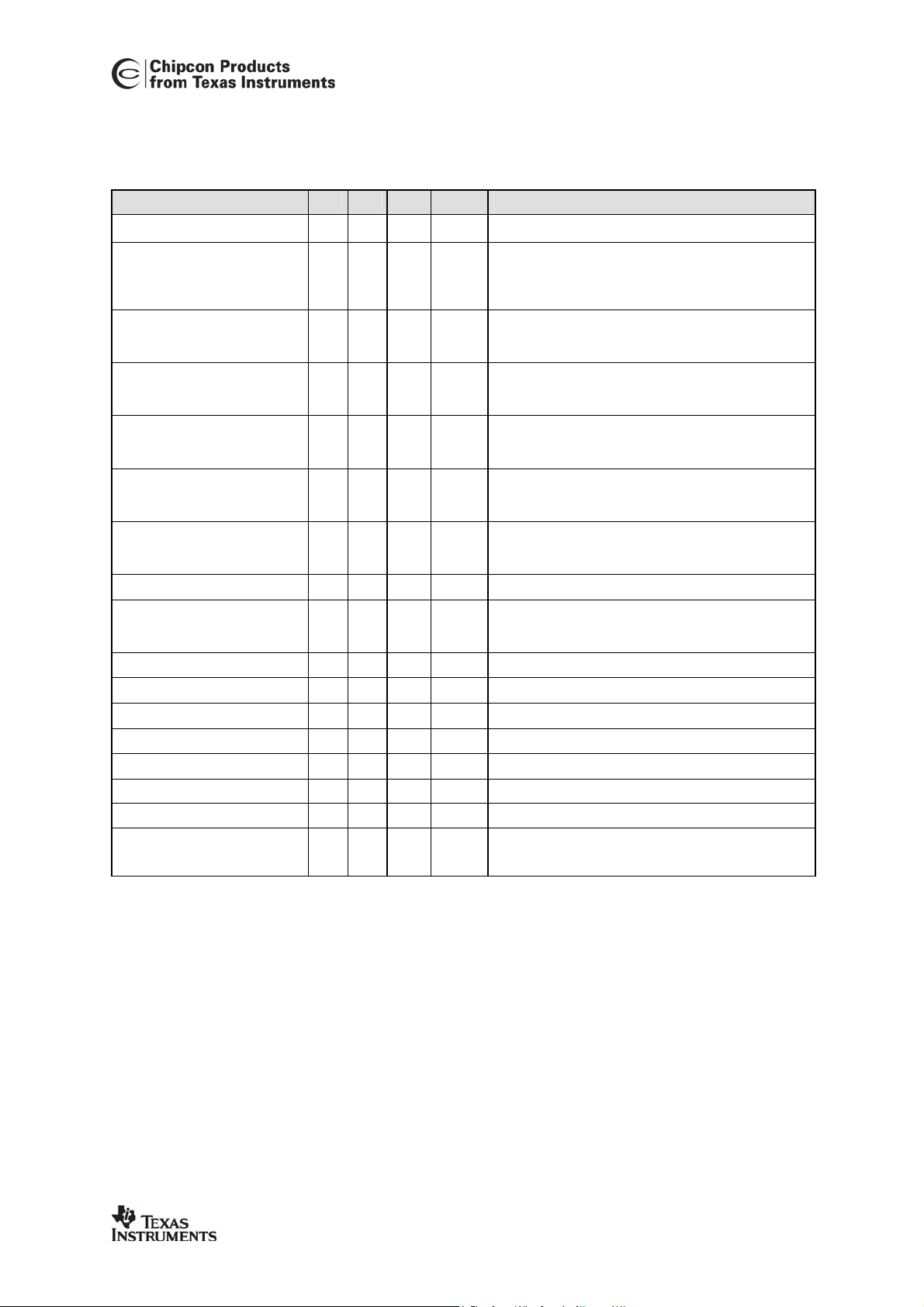
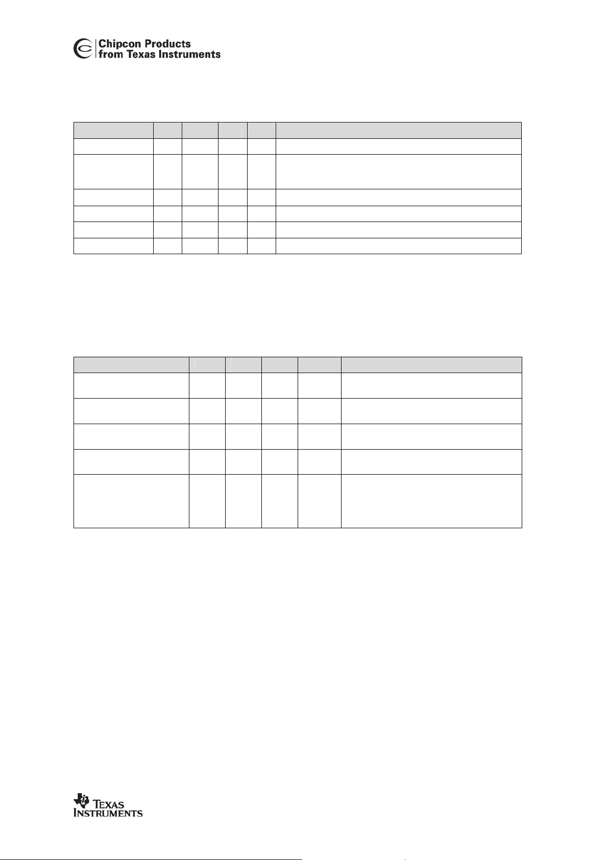
5 Absolute Maximum Ratings
Under no circumstances must the absolute maximum ratings given in Table 2 be violated. Stress
exceeding one or more of the limiting values may cause permanent damage to the device.
Parameter Min Max Units Condition
Supply voltage –0.3 3.6 V All supply pins must have the same voltage
Voltage on any digital pin –0.3 VDD+0.3,
Voltage on the 1.8V pins (pin no.
22, 25-40 and 42)
Input RF level 10 dBm
Storage temperature range –50 150
Reflow soldering temperature 260
–0.3 2.0 V
max 3.6
Table 2: Absolute Maximum Rati ngs
Caution! ESD sensitive device.
Precaution should be used when handling
the device in order to prevent permanent
damage.
V
Device not programmed
°C
According to IPC/JEDEC J-STD-020C
°C
CC2430
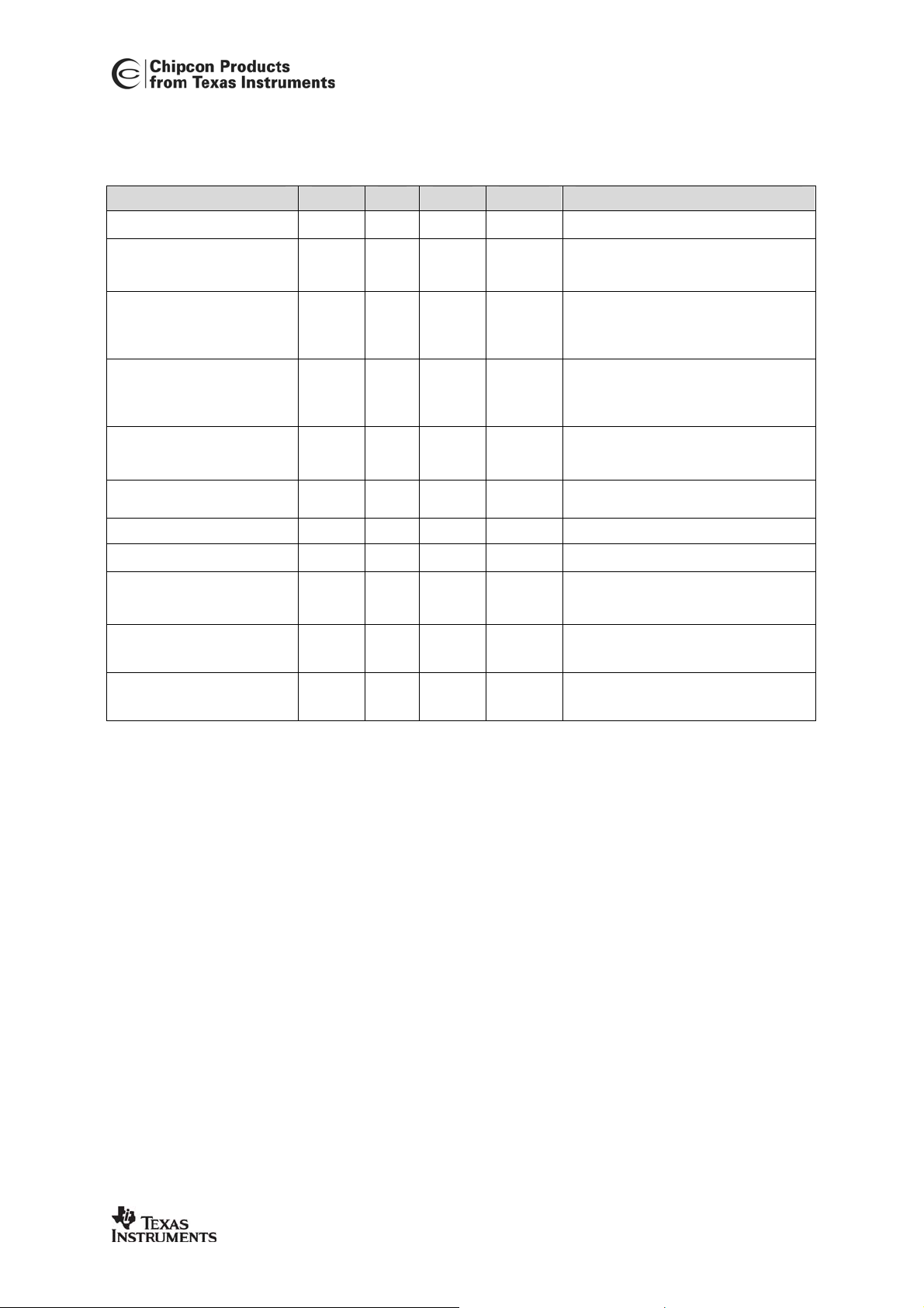
6 Operating Conditions
The operating conditions for
Parameter Min Max Unit Condition
Operating ambient temperature
range, T
Operating supply voltage 2.0 3.6 V The supply pins to the radio part must be driven
A
CC2430
are listed in Table 3 .
-40 85
Table 3: Operating Condi tions
°C
by the 1.8 V on-chip regulator
CC2430 PRELIMINARY Data Sheet (rev. 2.01) SWRS036E Page 10 of 233
This device is not yet released to market. Volume shipments possible under waiver.
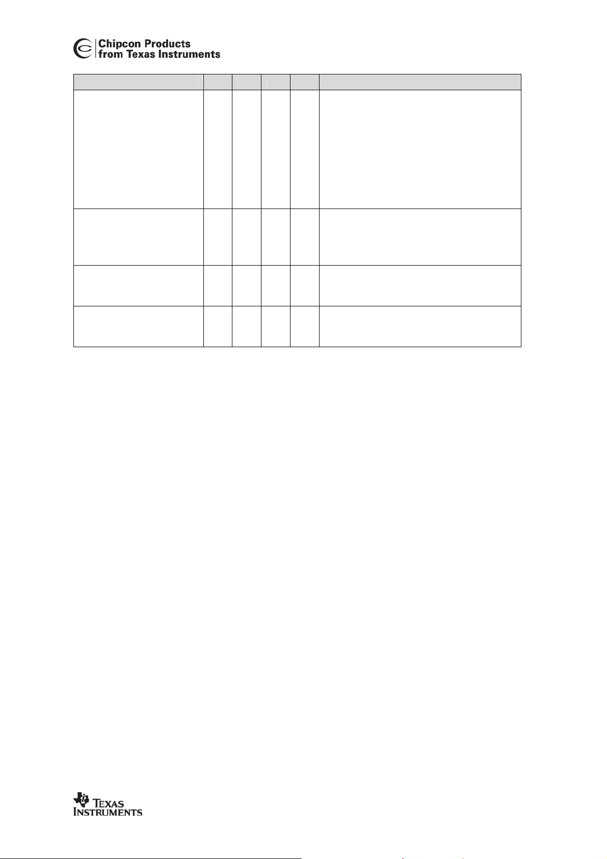
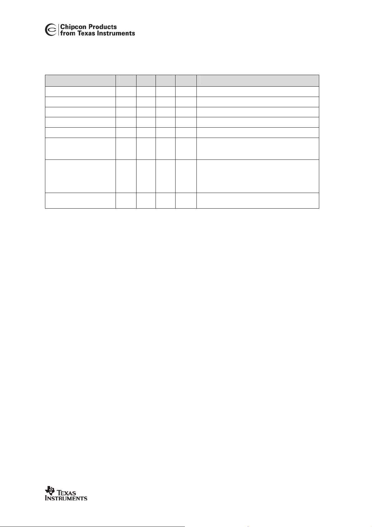
7 Electrical Specifications
CC2430
Measured on Texas Instruments
CC2430
EM reference design with TA=25°C and VDD=3.0V
unless stated otherwise.
Parameter Min Typ Max Unit Condition
Current Consumption
MCU Active Mode, 16 MHz 4.3 mA
MCU Active Mode, 32 MHz 9.5 mA
MCU Active and RX Mode 26.7 mA
MCU Active and TX Mode, 0dBm 26.9 mA
Power mode 1 190
Power mode 2 0.5
Power mode 3 0.3
Peripheral Current
Consumption
Timer 1 150
Timer 2 230
Timer 3 50
Timer 4 50
Sleep Timer 0.2
ADC 1.2 mA When converting.
Flash write 3 mA Estimated value
Flash erase 3 mA Estimated value
Digital regulator on, High frequency (16 MHz) RCOSC
running.
No radio, crystals, or peripherals active. Code run with
Cache hit.
MCU running at full speed (32MHz), 32MHz XOSC
running. No radio or peripherals active. Code run with
Cache hit.
MCU running at full speed (32MHz), 32MHz XOSC
running, radio in RX mode, -50 dBm input power. No
peripherals active. Code run with Cache hit.
MCU running at full speed (32MHz), 32MHz XOSC
running, radio in TX mode, 0dBm output power. No
peripherals active. Code run with Cache hit.
Digital regulator on, High frequency RCOSC and crystal
oscillator off. 32.768 kHz XOSC, POR and ST active.
µA
RAM retention.
Digital regulator off, High frequency RCOSC and crystal
oscillator off. 32.768 kHz XOSC, POR and ST active.
µA
RAM retention.
No clocks. RAM retention. POR active.
µA
Adds to the figures above if the peripheral unit is
activated
Timer running, 32MHz XOSC used.
µA
Timer running, 32MHz XOSC used.
µA
Timer running, 32MHz XOSC used.
µA
Timer running, 32MHz XOSC used.
µA
Including 32 kHz RCOSC or 32.768 kHz XOSC
µA
Table 4: Electrical Specifications
CC2430 PRELIMINARY Data Sheet (rev. 2.01) SWRS036E Page 11 of 233
This device is not yet released to market. Volume shipments possible under waiver.
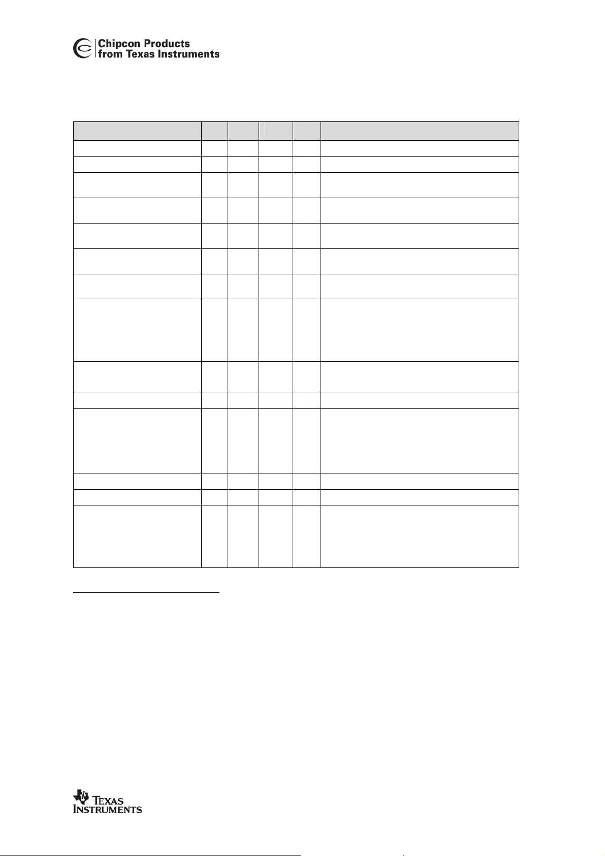
7.1 General Characteristics
CC2430
Measured on Texas Instruments
CC2430
EM reference design with TA=25°C and VDD=3.0V
unless stated otherwise.
Parameter Min Typ Max Unit Condition/Note
Wake-Up and Timing
Power mode 1 Æ power
mode 0
Power mode 2 or 3 Æ power
mode 0
Active Æ TX or RX
32MHz XOSC initially OFF.
Voltage regulator initially OFF
Active Æ TX or RX
Voltage regulator initially OFF
Active Æ RX or TX 192
RX/TX turnaround 192
Radio part
RF Frequency Range 2400 2483.5 MHz Programmable in 1 MHz steps, 5 MHz
Radio bit rate 250 kbps As defined by [1]
4.1
89.2
525
320
µs
µs
µs
µs
µs
µs
Digital regulator on, High frequency
RCOSC and crystal oscillator off. Startup of High frequency RCOSC.
Digital regulator off, High frequency
RCOSC and crystal oscillator off. Startup of regulator and High frequency
RCOSC.
Time from enabling radio part in power
mode 0, until TX or RX starts. Includes
start-up of voltage regulator and crystal
oscillator in parallel. Crystal ESR=16Ω.
Time from enabling radio part in power
mode 0, until TX or RX starts. Includes
start-up of voltage regulator.
Radio part already enabled.
Time until RX or TX starts.
between channels for compliance with
[1]
Radio chip rate
2.0 MChip/s As defined by [1]
Table 5: General Characteristics
CC2430 PRELIMINARY Data Sheet (rev. 2.01) SWRS036E Page 12 of 233

This device is not yet released to market. Volume shipments possible under waiver.
7.2 RF Receive Section
CC2430
Measured on Texas Instruments
CC2430
EM reference design with TA=25°C and VDD=3.0V
unless stated otherwise.
Parameter Min Typ Max Unit Condition/Note
Receiver sensitivity
Saturation (maximum input
level)
Adjacent channel rejection
+ 5 MHz channel spacing
Adjacent channel rejection
- 5 MHz channel spacing
Alternate channel rejection
+ 10 MHz channel spacing
Alternate channel rejection
- 10 MHz channel spacing
Channel rejection
≥ + 15 MHz
≤ - 15 MHz
Co-channel rejection
-91 dBm PER = 1%, as specified by [1]
Measured in 50 Ω single endedly through a balun.
[1] requires –85 dBm
10 dBm PER = 1%, as specified by [1]
Measured in 50 Ω single endedly through a balun.
[1] requires –20 dBm
41
30
55
53
55
53
-6
Wanted signal -88dBm, adjacent modulated channel
at
dB
+5 MHz, PER = 1 %, as specified by [1].
[1] requires 0 dB
Wanted signal -88dBm, adjacent modulated channel
at
dB
-5 MHz, PER = 1 %, as specified by [1].
[1] requires 0 dB
Wanted signal -88dBm, adjacent modulated channel
at
dB
+10 MHz, PER = 1 %, as specified by [1]
[1] requires 30 dB
Wanted signal -88dBm, adjacent modulated channel
at
dB
-10 MHz, PER = 1 %, as specified by [1]
[1] requires 30 dB
Wanted signal @ -82 dBm. Undesired signal is an
802.15.4 modulated channel, stepped through all
dB
channels from 2405 to 2480 MHz. Signal level for
PER = 1%. Values are estimated.
dB
Wanted signal @ -82 dBm. Undesired signal is
802.15.4 modulated at the same frequency as the
dB
desired signal. Signal level for PER = 1%.
CC2430 PRELIMINARY Data Sheet (rev. 2.01) SWRS036E Page 13 of 233
This device is not yet released to market. Volume shipments possible under waiver.
Parameter Min Typ Max Unit Condition/Note
Blocking / Desensitization
+ 5 MHz from band edge
+ 10 MHz from band edge
+ 20 MHz from band edge
+ 50 MHz from band edge
- 5 MHz from band edge
- 10 MHz from band edge
- 20 MHz from band edge
- 50 MHz from band edge
Spurious emission
30 – 1000 MHz
1 – 12.75 GHz
Frequency error tolerance ±140 ppm Difference between centre frequency of the received
Symbol rate error tolerance ±900 ppm Difference between incoming symbol rate and the
-42
-45
-26
-22
-31
-36
-24
-25
dBm
dBm
dBm
dBm
dBm
dBm
dBm
dBm
−64
dBm
−75
dBm
Wanted signal 3 dB above the sensitivity level, CW
jammer, PER = 1%. Measured according to EN 300
440 class 2.
Conducted measurement in a 50 Ω single ended
load. Complies with EN 300 328, EN 300 440 class
2, FCC CFR47, Part 15 and ARIB STD-T-66
RF signal and local oscillator frequency.
[1] requires minimum 80 ppm
internally generated symbol rate
[1] requires minimum 80 ppm
CC2430
Table 6: RF Receive Parameters
CC2430 PRELIMINARY Data Sheet (rev. 2.01) SWRS036E Page 14 of 233
This device is not yet released to market. Volume shipments possible under waiver.
7.3 RF Transmit Section
CC2430
Measured on Texas Instruments
CC2430
EM reference design with TA=25°C and VDD=3.0V
unless stated otherwise.
Parameter Min Typ Max Unit Condition/Note
Nominal output
power
Programmable
output power range
Harmonics
nd
harmonic
2
rd
harmonic
3
th
harmonic
4
th
harmonic
5
Spurious emission
30 - 1000 MHz
1– 12.75 GHz
1.8 – 1.9 GHz
5.15 – 5.3 GHz
Error Vector
Magnitude (EVM)
Optimum load
impedance
0 dBm
25.8 dB The output power is programmable in 16 steps from
-50.7
-55.8
-54.2
-53.4
-47
-43
-58
-56
11 % Measured as defined by [1]
115
+ j180
Delivered to a single ended 50 Ω load through a balun and
output power control set to 0x5F (TXCTRLL).
[1] requires minimum –3 dBm
approximately –25.2 to 0.6 dBm.
dBm
Measurement conducted with 100 kHz resolution bandwidth on
spectrum analyzer and output power control set to 0x5F
dBm
(TXCTRLL). Output Delivered to a single ended 50 Ω load
through a balun.
dBm
dBm
Maximum output power.
dBm
The peak conducted spurious emission is -47dBm@192MHz
which isin a EN300440 restricted band limited to -54dBm. All
dBm
radiated spurious emissions are within the limits of
ETSI/FCC/ARIB.
dBm
Texas Instruments
dBm
EN 300 328, EN 300 440, FCC CFR47 Part 15 and ARIB STDT-66
[1] requires max. 35 %
Ω
Differential impedance as seen from the RF-port (
RF_N
) towards the antenna.
CC2430
EM reference design complies with
RF_P
and
Table 7: RF Transmit Parameters
7.4 32 MHz Crystal Oscillator
Measured on Texas Instruments
CC2430
EM reference design with TA=25°C and VDD=3.0V
unless stated otherwise.
Parameter Min Typ Max Unit Condition/Note
Crystal frequency 32 MHz
Crystal frequency
accuracy
requirement
ESR 6 16 60
C0 1 1.9 7 pF
CL 10 13 16 pF Load capacitance is optionally tunable through software
Start-up time 212 µs
- 40
40 ppm Including aging and temperature dependency, as specified by [1]
Accuracy requirements can be relaxed by optional built-in tuning of
load capacitance through software
Ω
1
Table 8: 32 MHz Crystal Oscillator Parameters
1
Only for devices with Chip Version register, CHVER.VERSION equal to 0x02 or greater
CC2430 PRELIMINARY Data Sheet (rev. 2.01) SWRS036E Page 15 of 233
This device is not yet released to market. Volume shipments possible under waiver.
7.5 32.768 kHz Crystal Oscillator
CC2430
Measured on Texas Instruments
CC2430
EM reference design with TA=25°C and VDD=3.0V
unless stated otherwise.
Parameter Min Typ Max Unit Condition/Note
Crystal frequency 32.768 kHz
Crystal frequency
accuracy
requirement
ESR 40 130
C0 0.9 2.0 pF
CL 12 16 pF
Start-up time 450 ms Value is estimated.
–40 40 ppm Including aging and temperature dependency, as specified by [1]
kΩ
Table 9: 32.768 kHz Crystal Oscillator Parameters
7.6 32 kHz RC Oscillator
Measured on Texas Instruments
CC2430
EM reference design with TA=25°C and VDD=3.0V
unless stated otherwise.
Parameter Min Typ Max Unit Condition/Note
Calibrated frequency 32.753 kHz The calibrated 32 kHz RC Oscillator frequency
Frequency accuracy after
calibration
Temperature coefficient +0.4
Supply voltage coefficient +3 % / V Frequency drift when supply voltage changes
Initial calibration time 1.7 ms
±0.2 % Value is estimated.
% / °C
is the 32 MHz XTAL frequency divided by 977
Frequency drift when temperature changes
after calibration. Value is estimated.
after calibration. Value is estimated.
When the 32 kHz RC Oscillator is enabled,
calibration is continuously done in the
background as long as the 32 MHz crystal
oscillator is running and
SLEEP.OSC32K_CALDIS bit is cleared.
Table 10: 32 kHz RC Oscillator parameters
CC2430 PRELIMINARY Data Sheet (rev. 2.01) SWRS036E Page 16 of 233
This device is not yet released to market. Volume shipments possible under waiver.
7.7 High Frequency RC Oscillator
CC2430
Measured on Texas Instruments
CC2430
EM reference design with TA=25°C and VDD=3.0V
unless stated otherwise.
Parameter Min Typ Max Unit Condition/Note
Frequency 16 MHz The calibrated High Frequency RC Oscillator
Uncalibrated frequency
accuracy
Calibrated frequency
accuracy
Start-up time 10 µs
Temperature coefficient -325
Supply voltage coefficient 28
Initial calibration time 50 µs When the High Frequency RC Oscillator is
±18
±0.6 ±1
%
%
ppm / °C
ppm / mV
frequency is the 32 MHz XTAL frequency
multiplied by 1/2
CC2430
Measured on Texas Instruments
reference design.
Frequency drift when temperature changes
after calibration
Frequency drift when supply voltage changes
after calibration
enabled, calibration is continuously done in the
background as long as the crystal oscillator is
running.
EM
Table 11: High Frequency RC Oscillator parameters
7.8 Frequency Synthesizer Characteristics
Measured on Texas Instruments
CC2430
EM reference design with TA=25°C and VDD=3.0V
unless stated otherwise.
Parameter Min Typ Max Unit Condition/Note
Phase noise
−116
−117
−118
PLL lock time
192
dBc/Hz
dBc/Hz
dBc/Hz
µs
Unmodulated carrier
At ±1.5 MHz offset from carrier
At ±3 MHz offset from carrier
At ±5 MHz offset from carrier
The startup time when the crystal oscillator is running
and RX / TX turnaround time
Table 12: Frequency Synthesizer Parameters
CC2430 PRELIMINARY Data Sheet (rev. 2.01) SWRS036E Page 17 of 233
This device is not yet released to market. Volume shipments possible under waiver.
7.9 Analog Temperature Sensor
CC2430
Measured on Texas Instruments
CC2430
EM reference design with TA=25°C and VDD=3.0V
unless stated otherwise.
Parameter Min Typ Max Unit Condition/Note
Output voltage at –40°C
Output voltage at 0°C
Output voltage at +40°C
Output voltage at +80°C
Temperature coefficient 2.45
Absolute error in calculated
temperature
Error in calculated
temperature, calibrated
Current consumption
increase when enabled
0.648 V Values are estimated
0.743 V Values are estimated
0.840 V Values are estimated
0.939 V Values are estimated
mV/°C Fitted from –20°C to +80°C on estimated values.
–8
-2 0 2
280 µA
°C From –20°C to +80°C when assuming best fit for
absolute accuracy on estimated values: 0.743V at
0°C and 2.45mV / °C.
°C From –20°C to +80°C when using 2.45mV / °C,
after 1-point calibration at room temperature.
Values are estimated. Indicated min/max with 1point calibration is based on simulated values for
typical process parameters
Table 13: Analog Temperature Sensor Parameters
CC2430 PRELIMINARY Data Sheet (rev. 2.01) SWRS036E Page 18 of 233
7.10 ADC
This device is not yet released to market. Volume shipments possible under waiver.
CC2430
Measured on Texas Instruments
CC2430
EM reference design with TA=25°C, VDD=3.0V.
Preliminary characterized parameters.
Parameter Min Typ Max Unit Condition/Note
Input voltage 0 AVDD V AVDD is voltage on AVDD_SOC pin
External reference voltage 0 AVDD V AVDD is voltage on AVDD_SOC pin
External reference voltage
differential
Input resistance, ADC singleended input
Input resistance, ADC
differential input
Input resistance, single-ended
reference
Input resistance, differential
reference
Effective number of bits 5.5 bits 8-bits setting.
(ENOB)2 7.3 10-bits setting.
9.0 12-bits setting.
10.5 14-bits setting.
Effective number of bits (ENOB)
Differential input
Offset1 TBD LSB
Conversion time 20
36
68
132
Differential nonlinearity (DNL)3 ±0.14 1.0 LSB 8-bits setting.
Integral nonlinearity (INL) 2 ±0.5 3.4 LSB 8-bits setting.
SINAD2 34 dB 8-bits setting.
(sine input signal 46 dB 10-bits setting.
frequency 1 Hz and 1 kHz) 56 dB 12-bits setting.
65 dB 14-bits setting.
2
1
1
0 AVDD V AVDD is voltage on AVDD_SOC pin
167 kΩ AIN0 to AIN7 selected as ADC input
TBD
49 kΩ AIN7 selected as external reference input
TBD
TBD
8-bits setting.
µs
10-bits setting.
µs
12-bits setting.
µs
14-bits setting.
µs
Table 14: ADC Characteristics
2
Not characterized for this data sheet revision.
3
Single-ended input signal and AVDD used as reference. Sine input, tested at frequencies 1 Hz and 1 kHz
CC2430 PRELIMINARY Data Sheet (rev. 2.01) SWRS036E Page 19 of 233
This device is not yet released to market. Volume shipments possible under waiver.
7.11 Control AC Characteristics
= -40°C to 85°C, VDD=3.0V if nothing else stated.
T
A
Parameter Min Typ Max Unit Condition/Note
CC2430
System clock,
f
SYSCLK
= 1/ f
t
SYSCLK
RESET_N low
width
Interrupt pulse
width
SYSCLK
16 32 MHz System clock is when 32 MHz crystal oscillator is used.
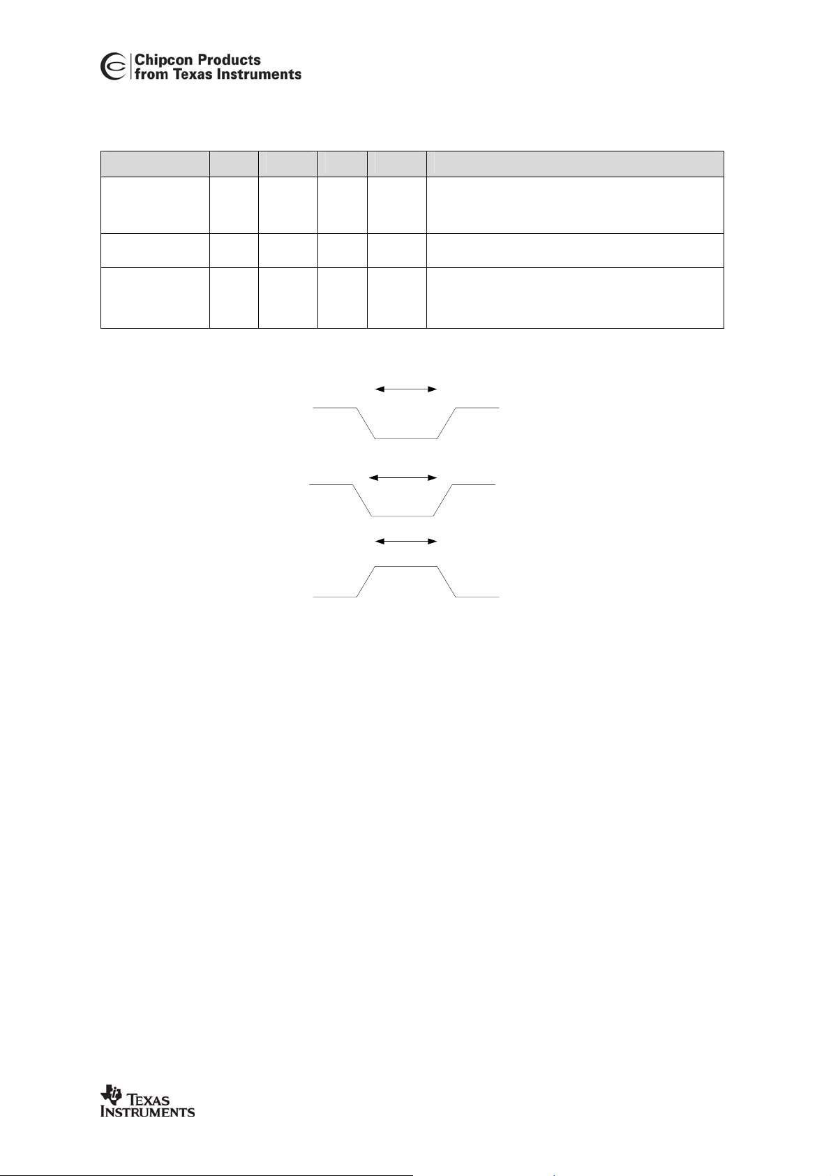
2.5 ns See item 1, Figure 1. This is the shortest pulse that is
t
ns See item 2, Figure 1.This is the shortest pulse that is
SYSCLK
System clock is 16 MHz when high frequency RC
oscillator is used.
guaranteed to be recognized as a reset pin request.
guaranteed to be recognized as an interrupt request. In
PM2/3 the internal synchronizers are bypassed so this
requirement does not apply in PM2/3.
Table 15: Control Inputs AC Characteristics
1
RESET_N
Px.n
Px.n
2
2
Figure 1: Control Inputs AC Characteristics
CC2430 PRELIMINARY Data Sheet (rev. 2.01) SWRS036E Page 20 of 233
This device is not yet released to market. Volume shipments possible under waiver.
7.12 SPI AC Characteristics
= -40°C to 85°C, VDD=3.0V if nothing else stated.
T
A
Parameter Min Typ Max Unit Condition/Note
CC2430
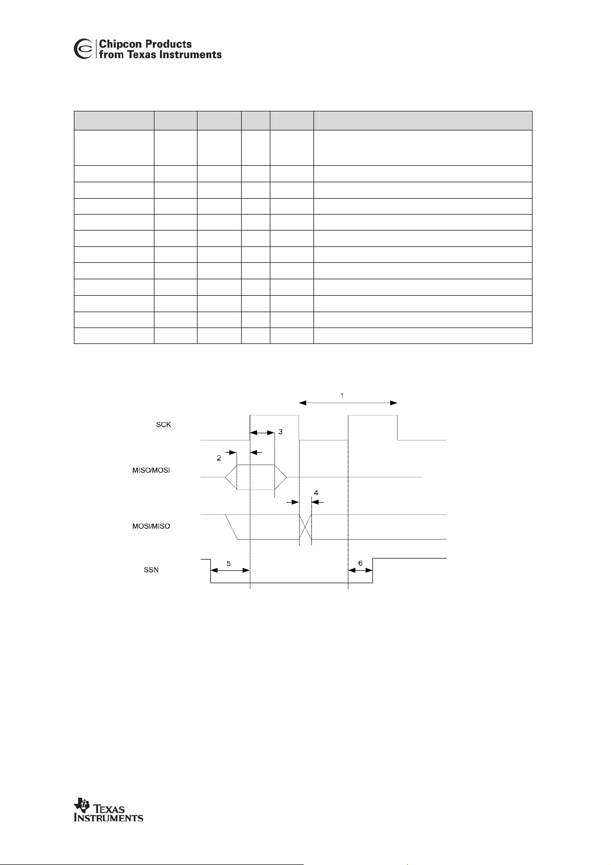
SCK period See
SCK duty cycle 50%
SSN low to SCK 2*t
SCK to SSN high 30 ns See item 6 Figure 2
MISO setup 10 ns Master. See item 2 Figure 2
MISO hold 10 ns Master. See item 3 Figure 2
SCK to MOSI 25 ns Master. See item 4 Figure 2, load = 10 pF
SCK period 100 ns Slave. See item 1 Figure 2
SCK duty cycle 50%
MOSI setup 10 ns Slave. See item 2 Figure 2
MOSI hold 10 ns Slave. See item 3 Figure 2
SCK to MISO 25 ns Slave. See item 4 Figure 2, load = 10 pF
SYSCLK
section
13.13.3
See item 5 Figure 2
ns Master. See item 1 Figure 2
Master.
Slave.
Table 16: SPI AC Characteristics
Figure 2: SPI AC Characteristics
CC2430 PRELIMINARY Data Sheet (rev. 2.01) SWRS036E Page 21 of 233
This device is not yet released to market. Volume shipments possible under waiver.
7.13 Debug Interface AC Characteristics
= -40°C to 85°C, VDD=3.0V if nothing else stated.
T
A
Parameter Min Typ Max Unit Condition/Note
CC2430
Debug clock
period
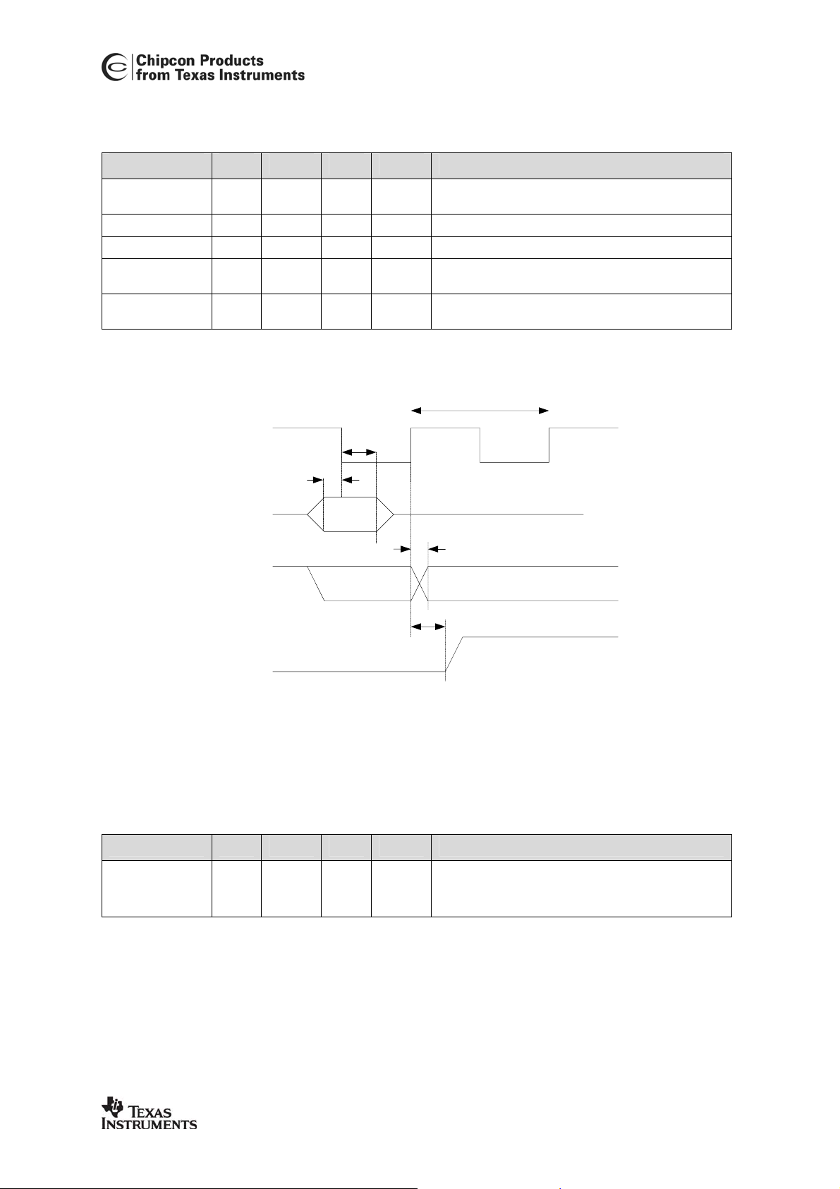
Debug data setup 5 ns See item 2 Figure 3
Debug data hold 5 ns See item 3 Figure 3
Clock to data
delay
RESET_N inactive
after P2_2 rising
128 ns See item 1 Figure 3
10 ns See item 4 Figure 3, load = 10 pF
10 ns See item 5 Figure 3
Table 17: Debug Interface AC Characteristics
1
DEBUG CLK
P2_2
2
DEBUG DATA
P2_1
DEBUG DATA
P2_1
3
4
RESET_N
5
Figure 3: Debug Interface AC Characteristics
7.14 Port Outputs AC Characteristics
T
= -40°C to 85°C, VDD=3.0V if nothing else stated.
A
Parameter Min Typ Max Unit Condition/Note
P0, P1, P2 Port
output pins, rise
and fall time
10 ns Load = 10 pF
Timing is with respect to 10% VDD and 90% VDD levels.
Value is estimated
Table 18: Port Outputs AC Characteristics
CC2430 PRELIMINARY Data Sheet (rev. 2.01) SWRS036E Page 22 of 233
This device is not yet released to market. Volume shipments possible under waiver.
7.15 Timer Inputs AC Characteristics
= -40°C to 85°C, VDD=3.0V if nothing else stated.
T
A
Parameter Min Typ Max Unit Condition/Note
CC2430
Input capture
pulse width
t
ns Synchronizers determine the shortest input pulse that
SYSCLK
can be recognized. The synchronizers operate at the
current system clock rate (16 or 32 MHz)
Table 19: Timer Inputs AC Characteristics
7.16 DC Characteristics
The DC Characteristics of
=25°C, VDD=3.0V if nothing else stated.
T
A
Digital Inputs/Outputs Min Typ Max Unit Condition
Logic "0" input voltage 0 0.7 0.9 V
Logic "1" input voltage VDD-0.7 VDD VDD V
Logic "0" output voltage 0 0 0.25 V For up to 4mA output current on all pins except
Logic "1" output voltage VDD-0.25 VDD VDD V For up to 4mA output current on all pins except
Logic "0" input current NA –1 –1
Logic "1" input current NA 1 1
I/O pin pull-up and pull-down
resistor
CC2430
are listed in Table 20 below.
17 20 23 kΩ
P1_0 and P1_1 which are up to 20 mA
P1_0 and P1_1 which are up to 20 mA
Input equals 0V
µA
Input equals VDD
µA
Table 20: DC Characteristics
CC2430 PRELIMINARY Data Sheet (rev. 2.01) SWRS036E Page 23 of 233
This device is not yet released to market. Volume shipments possible under waiver.
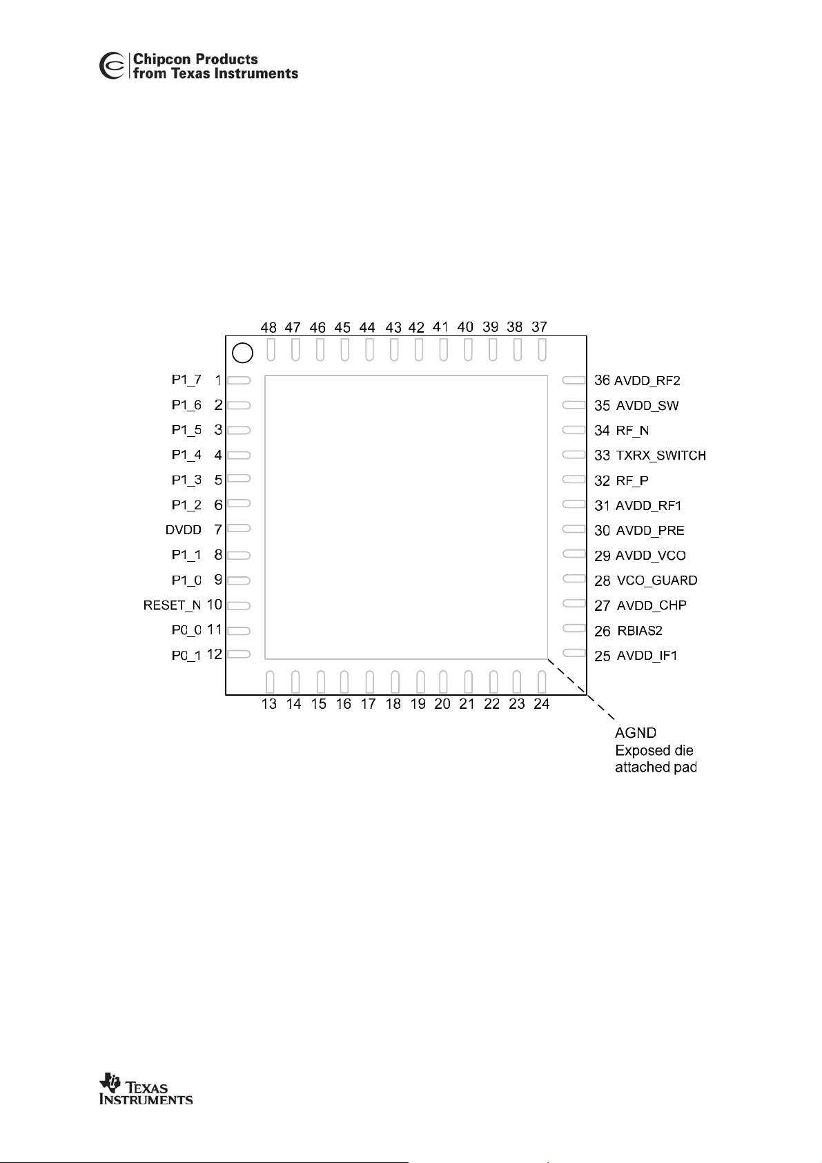
8 Pin and I/O Port Configuration
The
CC2430
configuration of digital I/O ports.
pinout is shown in Figure 4 and Table 21. See section 13.1 for details on the
CC2430
P0_2
P2_0
DVDD
P0_3
P0_4
P2_1
P0_5
P2_2
P2_3/XOSC_Q1
P0_6
P2_4/XOSC_Q2
P0_7
AVDD_DREG
DCOUPL
XOSC_Q2
AVDD_SOC
AVDD_DGUARD
DVDD_ADC
AVDD_ADC
AVDD_IF2
XOSC_Q1
RBIAS1
AVDD_RREG
RREG_OUT
Figure 4: Pinout top view
Note: The exposed die attach pad must be connected to a solid ground plane as this is the
ground connection for the chip.
CC2430 PRELIMINARY Data Sheet (rev. 2.01) SWRS036E Page 24 of 233
This device is not yet released to market. Volume shipments possible under waiver.
Pin Pin name Pin type Description
- GND Ground The exposed die attach pad must be connected to a solid ground plane
1 P1_7 Digital I/O Port 1.7
2 P1_6 Digital I/O Port 1.6
3 P1_5 Digital I/O Port 1.5
4 P1_4 Digital I/O Port 1.4
5 P1_3 Digital I/O Port 1.3
6 P1_2 Digital I/O Port 1.2
7 DVDD Power (Digital) 2.0V-3.6V digital power supply for digital I/O
8 P1_1 Digital I/O Port 1.1 – 20 mA drive capability
9 P1_0 Digital I/O Port 1.0 – 20 mA drive capability
10 RESET_N Digital input Reset, active low
11 P0_0 Digital I/O Port 0.0
12 P0_1 Digital I/O Port 0.1
13 P0_2 Digital I/O Port 0.2
14 P0_3 Digital I/O Port 0.3
15 P0_4 Digital I/O Port 0.4
16 P0_5 Digital I/O Port 0.5
17 P0_6 Digital I/O Port 0.6
18 P0_7 Digital I/O Port 0.7
19 XOSC_Q2 Analog I/O 32 MHz crystal oscillator pin 2
20 AVDD_SOC Power (Analog) 2.0V-3.6V analog power supply connection
21 XOSC_Q1 Analog I/O 32 MHz crystal oscillator pin 1, or external clock input
22 RBIAS1 Analog I/O External precision bias resistor for reference current
23 AVDD_RREG Power (Analog) 2.0V-3.6V analog power supply connection
24 RREG_OUT Power output 1.8V Voltage regulator power supply output. Only intended for supplying the analog
25 AVDD_IF1 Power (Analog) 1.8V Power supply for the receiver band pass filter, analog test module, global bias
26 RBIAS2 Analog output
27 AVDD_CHP Power (Analog) 1.8V Power supply for phase detector, charge pump and first part of loop filter
28 VCO_GUARD Power (Analog) Connection of guard ring for VCO (to AVDD) shielding
29 AVDD_VCO Power (Analog) 1.8V Power supply for VCO and last part of PLL loop filter
30 AVDD_PRE Power (Analog) 1.8V Power supply for Prescaler, Div-2 and LO buffers
31 AVDD_RF1 Power (Analog) 1.8V Power supply for LNA, front-end bias and PA
32 RF_P RF I/O Positive RF input signal to LNA during RX. Positive RF output signal from PA during
33 TXRX_SWITCH Power (Analog) Regulated supply voltage for PA
34 RF_N RF I/O Negative RF input signal to LNA during RX
35 AVDD_SW Power (Analog) 1.8V Power supply for LNA / PA switch
36 AVDD_RF2 Power (Analog) 1.8V Power supply for receive and transmit mixers
37 AVDD_IF2 Power (Analog) 1.8V Power supply for transmit low pass filter and last stages of VGA
38 AVDD_ADC Power (Analog) 1.8V Power supply for analog parts of ADCs and DACs
39 DVDD_ADC Power (Digital) 1.8V Power supply for digital parts of ADCs
40 AVDD_DGUARD Power (Digital) Power supply connection for digital noise isolation
41 AVDD_DREG Power (Digital) 2.0V-3.6V digital power supply for digital core voltage regulator
42 DCOUPL Power (Digital) 1.8V digital power supply decoupling. Do not use for supplying external circuits.
43 P2_4/XOSC_Q2 Digital I/O Port 2.4/32.768 kHz XOSC
44 P2_3/XOSC_Q1 Digital I/O Port 2.3/32.768 kHz XOSC
45 P2_2 Digital I/O Port 2.2
46 P2_1 Digital I/O Port 2.1
47 DVDD Power (Digital) 2.0V-3.6V digital power supply for digital I/O
48 P2_0 Digital I/O Port 2.0
1.8V part (power supply for pins 25, 27-31, 35-40).
and first part of the VGA
External precision resistor, 43 kΩ, ±1 %
TX
Negative RF output signal from PA during TX
CC2430
Table 21: Pinout overview
CC2430 PRELIMINARY Data Sheet (rev. 2.01) SWRS036E Page 25 of 233
This device is not yet released to market. Volume shipments possible under waiver.
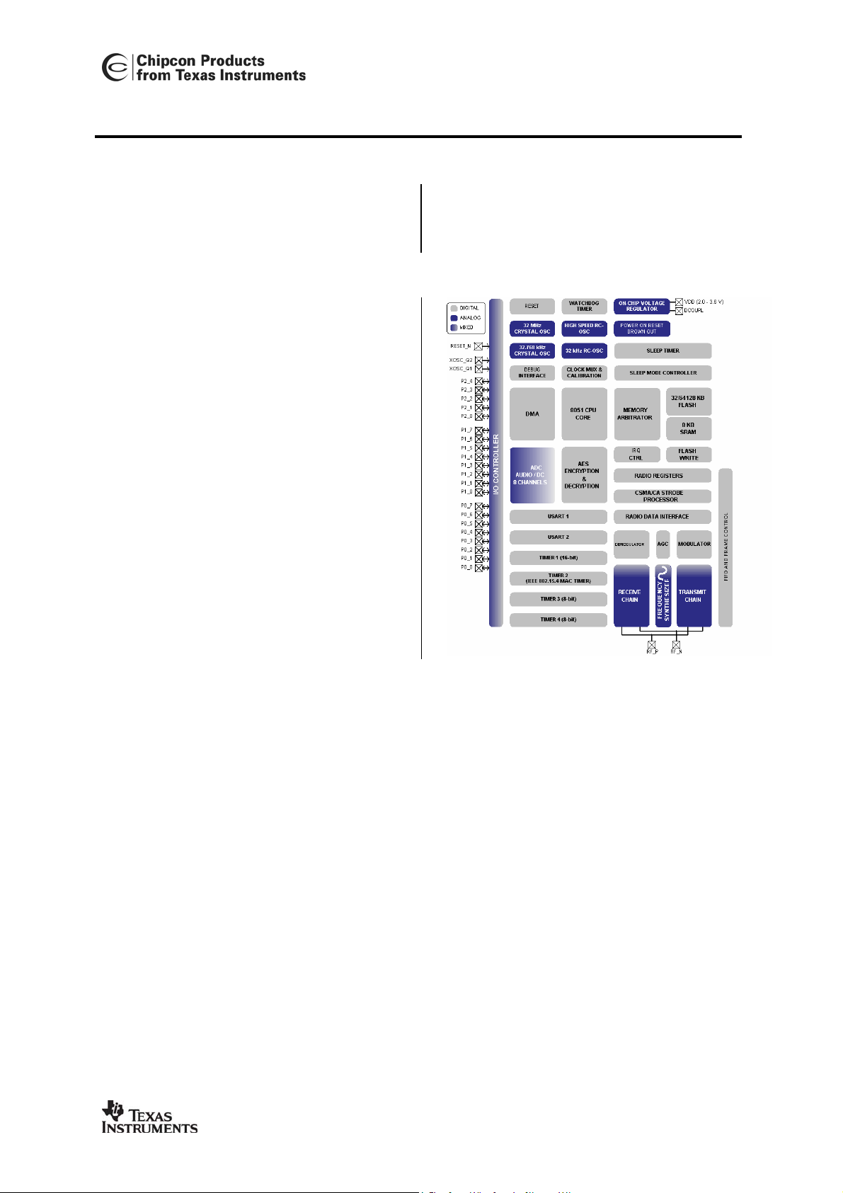
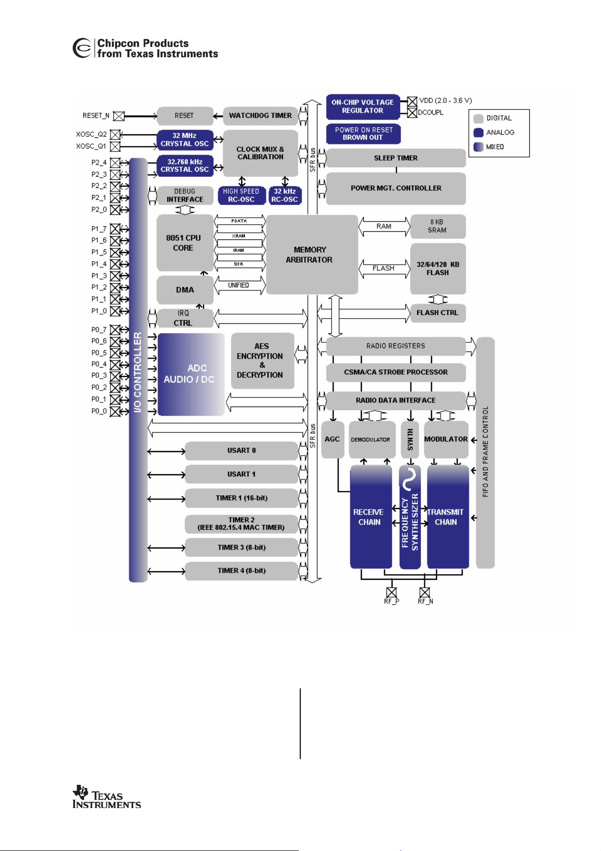
9 Circuit Description
CC2430
Figure 5:
A block diagram of
5. The modules can be roughly divided into
one of three categories: CPU-related modules,
radio-related modules and modules related to
power, test and clock distribution. In the
following subsections, a short description of
CC2430
is shown in Figure
CC2430 PRELIMINARY Data Sheet (rev. 2.01) SWRS036E Page 26 of 233
CC2430
Block Diagram
each module that appears in Figure 5 is given.
9.1 CPU and Peripherals
The 8051 CPU core is a single-cycle 8051-
compatible core. It has three different memory

This device is not yet released to market. Volume shipments possible under waiver.
CC2430
access buses (SFR, DATA and
CODE/XDATA), a debug interface and an 18input extended interrupt unit. See section 12
for details on the CPU.
The memory crossbar/arbitrator is at the
heart of the system as it connects the CPU
and DMA controller with the physical
memories and all peripherals through the SFR
bus. The memory arbitrator has four memory
access points, access at which can map to
one of three physical memories: an 8 KB
SRAM, flash memory or RF and SFR
registers. The memory arbitrator is responsible
for performing arbitration and sequencing
between simultaneous memory accesses to
the same physical memory.
The SFR bus is drawn conceptually in the
block diagram as a common bus that connects
all hardware peripherals to the memory
arbitrator. The SFR bus in the block diagram
also provides access to the radio registers in
the radio register bank even though these are
indeed mapped into XDATA memory space.
The 8 KB SRAM maps to the DATA memory
space and to parts of the XDATA memory
spaces. 4 KB of the 8 KB SRAM is an ultralow-power SRAM that retains its contents even
when the digital part is powered off (power
modes 2 and 3). The rest of the SRAM loses
its contents when the digital part is powered
off.
The 32/64/128 KB flash block provides in-
circuit programmable non-volatile program
memory for the device and maps into the
CODE and XDATA memory spaces. Table 22
shows the available devices in the
family. The available devices differ only in
flash memory size. Writing to the flash block is
performed through a flash controller that
allows page-wise (2048 byte) erasure and 4
byte-wise programming. See section 13.14 for
details on the flash controller.
A versatile five-channel DMA controller is
available in the system and accesses memory
using a unified memory space (XDATA) and
thus has access to all physical memories.
Each channel is configured (trigger, priority,
transfer mode, addressing mode, source and
destination pointers, and transfer count) with
DMA descriptors anywhere in memory. Many
of the hardware peripherals rely on the DMA
controller for efficient operation (AES core,
flash write controller, USARTs, Timers, ADC
interface) by performing data transfers
between a single SFR address and
flash/SRAM. See section 13.2 for details.
CC2430
The interrupt controller services a total of 18
interrupt sources, divided into six interrupt
groups, each of which is associated with one
of four interrupt priorities. An interrupt request
is serviced even if the device is in a sleep
mode (power modes 1-3) by bringing the
CC2430
The debug interface implements a proprietary
two-wire serial interface that is used for incircuit debugging. Through this debug
interface it is possible to perform an erasure of
the entire flash memory, control which
oscillators are enabled, stop and start
execution of the user program, execute
supplied instructions on the 8051 core, set
code breakpoints, and single step through
instructions in the code. Using these
techniques it is possible to elegantly perform
in-circuit debugging and external flash
programming. See section 12.9 for details.
The I/O-controller is responsible for all
general-purpose I/O pins. The CPU can
configure whether peripheral modules control
certain pins or whether they are under
software control, and if so whether each pin is
configured as an input or output and if a pullup or pull-down resistor in the pad is
connected. Each peripheral that connects to
the I/O-pins can choose between two different
I/O pin locations to ensure flexibility in various
applications. See section 13.1 for details.
The sleep timer is an ultra-low power timer
that counts 32.768 kHz crystal oscillator or
32.768 kHz RC oscillator periods. The sleep
timer runs continuously in all operating modes
except power mode 3. Typical uses for it is as
a real-time counter that runs regardless of
operating mode (except power mode 3) or as a
wakeup timer to get out of power mode 1 or 2.
See section 13.5 for details.
A built-in watchdog timer allows the
to reset itself in case the firmware hangs.
When enabled by software, the watchdog
timer must be cleared periodically, otherwise it
will reset the device when it times out. See
section 13.12 for details.
Timer 1 is a 16-bit timer with
timer/counter/PWM functionality. It has a
programmable prescaler, a 16-bit period value
and three individually programmable
counter/capture channels each with a 16-bit
compare value. Each of the counter/capture
channels can be used as PWM outputs or to
capture the timing of edges on input signals.
See section 13.3 for details.
back to active mode (power mode 0).
CC2430
CC2430 PRELIMINARY Data Sheet (rev. 2.01) SWRS036E Page 27 of 233
This device is not yet released to market. Volume shipments possible under waiver.
CC2430
Timer 2 (MAC timer) is specially designed for
supporting an IEEE 802.15.4 MAC or other
time-slotted protocols in software. The timer
has a configurable timer period and an 8-bit
overflow counter that can be used to keep
track of the number of periods that have
transpired. There is also a 16-bit capture
register used to record the exact time at which
a start of frame delimiter is
received/transmitted or the exact time of which
transmission ends, as well as a 16-bit output
compare register that can produce various
command strobes (start RX, start TX, etc) at
specific times to the radio modules. See
section 13.4 for details.
Timers 3 and 4 are 8-bit timers with
timer/counter/PWM functionality. They have a
programmable prescaler, an 8-bit period value
and one programmable counter channel with a
8-bit compare value. Each of the counter
channels can be used as PWM outputs. See
section 13.6 for details.
USART 0 and 1 are each configurable as
either an SPI master/slave or a UART. They
provide double buffering on both RX and TX
and hardware flow-control and are thus well
suited to high-throughput full-duplex
applications. Each has its own high-precision
baud-rate generator thus leaving the ordinary
timers free for other uses. When configured as
an SPI slave they sample the input signal
using SCK directly instead of some oversampling scheme and are thus well-suited to
high data rates. See section 13.13 for details.
The AES encryption/decryption core allows
the user to encrypt and decrypt data using the
AES algorithm with 128-bit keys. The core is
able to support the AES operations required
by IEEE 802.15.4 MAC security, the ZigBee™
network layer and the application layer. See
section 13.9 for details.
The ADC supports 8 to 14 bits of resolution in
a 30 kHz to 4 kHz bandwidth respectively. DC
and audio conversions with up to 8 input
channels (Port 0) are possible. The inputs can
be selected as single ended or differential.
The reference voltage can be internal, AVDD,
or a single ended or differential external signal.
The ADC also has a temperature sensor input
channel. The ADC can automate the process
of periodic sampling or conversion over a
sequence of channels. See Section 13.7 for
details.
9.2 Radio
CC2430
radio based on the leading
transceiver. See Section 14 for details.
features an IEEE 802.15.4 compliant
CC2420
Device Flash
CC2430-F32 32 KB
CC2430-F64 64 KB
CC2430-F128 128 KB
Table 22: CC2430 Flash Memory Options
CC2430 PRELIMINARY Data Sheet (rev. 2.01) SWRS036E Page 28 of 233
This device is not yet released to market. Volume shipments possible under waiver.
10 Power Management
CC2430
The
CC2430
has four major power modes,
called PM0, PM1, PM2 and PM3. PM0 is the
active mode while PM3 has the lowest power
consumption. The power modes are shown in
Table 23 together with voltage regulator and
oscillator options.
Power
Mode
PM0 B, C, D B, C B
PM1 A B, C B
PM2 A B, C A
PM3 A A A
High
frequency
oscillator
A None
B 32 MHz
C HF
D Both
Configuration
XOSC
RCOSC
Low- frequency
oscillator
A None
B 32.768
kHz
RCOSC
C 32.768
kHz
XOSC
Voltage
regulator
(digital)
A Off
B On
Table 23: Power Modes
PM0 : The full functional mode. The voltage
regulator to the digital core is on and either the
High frequency RC oscillator or the 32 MHz
crystal oscillator or both are running. Either the
32.768 kHz RC oscillator or the 32.768 kHz
crystal oscillator is running.
PM1 : The voltage regulator to the digital part
is on. Neither the 32 MHz crystal oscillator nor
the High frequency RC oscillator are running.
Either the 32.768 kHz RC oscillator or the
32.768 kHz crystal oscillator is running. The
system will go to PM0 on reset or an external
interrupt or when the sleep timer expires.
PM2 : The voltage regulator to the digital core
is turned off. Neither the 32 MHz crystal
oscillator nor the High frequency RC oscillator
are running. Either the 32.768 kHz RC
oscillator or the 32.768 kHz crystal oscillator is
running. The system will go to PM0 on reset or
an external interrupt or when the sleep timer
expires.
PM3 : The voltage regulator to the digital core
is turned off. None of the oscillators are
running. The system will go to PM0 on reset or
an external interrupt.
Refer to section 13.10 on page 135 for a
detailed description of power management.
CC2430 PRELIMINARY Data Sheet (rev. 2.01) SWRS036E Page 29 of 233

This device is not yet released to market. Volume shipments possible under waiver.
11 Application Circuit
CC2430
Few external components are required for the
operation of
circuit is shown in Figure 6. Typical values and
description of external components are shown
in Table 24
11.1 Input / output matching
The RF input/output is high impedance and
differential. The optimum differential load for
the RF port is 115+j180 Ω.
When using an unbalanced antenna such as a
monopole, a balun should be used in order to
optimize performance. The balun can be
implemented using low-cost discrete inductors
and capacitors. The recommended balun
shown, consists of C341, L341, L321 and
L331 together with a PCB microstrip
transmission line (λ/2-dipole), and will match
the RF input/output to 50 Ω. An internal T/R
switch circuit is used to switch between the
LNA and the PA. See Input/output matching
section on page 181 for more details.
If a balanced antenna such as a folded dipole
is used, the balun can be omitted. If the
antenna also provides a DC path from
TXRX_SWITCH pin to the RF pins, inductors
are not needed for DC bias.
CC2430
. A typical application
The load capacitance is optionally tunable
through software
accuracy. The tuning adds the capacitance,
C
shown in the equation above. Hence
tune
initial crystal inaccuracy may compensated for
by tuning. See page 63 for details about
tuning.
XTAL2 is an optional 32.768 kHz crystal, with
two loading capacitors (C441 and C431), used
for the 32.768 kHz crystal oscillator. The
32.768 kHz crystal oscillator is used in
applications where you need both very low
sleep current consumption and accurate wake
up times. The load capacitance seen by the
32.768 kHz crystal is given by:
C +
=
11.4 Voltage regulators
The on chip voltage regulators supply all 1.8 V
power supply pins and internal power supplies.
C241 and C421 are required for stability of the
regulators. A series resistor may be used to
comply with the ESR requirement.
4
to improve the frequency
1
+
CC
C
11
431441
parasiticL
Figure 6 shows a suggested application circuit
using a differential antenna. The antenna type
is a standard folded dipole. The dipole has a
virtual ground point; hence bias is provided
without degradation in antenna performance.
Also refer to the section Antenna
Considerations on page 186.
11.2 Bias resistors
The bias resistors are R221 and R261. The
bias resistor R221 is used to set an accurate
bias current for the 32 MHz crystal oscillator.
11.3 Crystal
An external 32 MHz crystal, XTAL1, with two
loading capacitors (C191 and C211) is used
for the 32 MHz crystal oscillator. See page 15
for details. The load capacitance seen by the
32 MHz crystal is given by:
C ++
=
1
11
+
CC
211191
CC
tuneparasiticL
11.5 Debug interface
The debug interface pin P2_2 is connected
through pull-up resistor R451 to the power
supply. See section 13.1.6 on page 74.
11.6 Power supply decoupling and
filtering
Proper power supply decoupling must be used
for optimum performance. The placement and
size of the decoupling capacitors and the
power supply filtering are very important to
achieve the best performance in an
application. TI provides a compact reference
design that should be followed very closely.
Refer to the section PCB Layout
Recommendation on page 185.
4
Only for devices with Chip Version register,
CHVER.VERSION equal to 0x02 or greater
CC2430 PRELIMINARY Data Sheet (rev. 2.01) SWRS036E Page 30 of 233

This device is not yet released to market. Volume shipments possible under waiver.
CC2430
optional
1
P1_7
2
P1_6
3
P1_5
4
P1_4
5
P1_3
P1_2
6
7
DVDD
P1_1
8
9
P1_0
RESET_N
10
11
P0_0
P0_1
12
P0_2
13
C441
C431
XTAL2
R451
48
47
46
45
44
P2_0
P2_1
DVDD
P2_3
P2_2
QLP48
CC2430
7x7
P0_3
14
P0_4
15
16
P0_5
P0_6
17
P0_7
18
43
P2_4
C421
2.0 - 3.6V Power Supply
42
41
40
DCOUPL
AVDD_DREG
AVDD_DGUARD
AVDD_SOC
XOSC_Q2
XOSC_Q1
RBIAS1
20
21
19
XTAL1
22
39
38
AVDD_ADC
DVDD_ADC
TXRX_SWITCH
VCO_GUARD
AVDD_RREG
23
R221
C241
37
AVDD_IF2
AVDD_RF2
AVDD_SW
RF_N
RF_P
AVDD_RF1
AVDD_PRE
AVDD_VCO
AVDD_CHP
RBIAS2
RREG_OUT
AVDD_IF1
24
Antenna
36
35
34
33
32
31
30
29
28
27
26
25
L321
L331
λ/4
R261
L341
λ/4
(50 Ohm)
C341
or
Folded Dipole PCB
Antenna
L331
L321
C211C191
Figure 6: CC2430 Application Circuit. (Digital I/O and ADC interface not connected).
Decoupling capacitors not shown.
CC2430 PRELIMINARY Data Sheet (rev. 2.01) SWRS036E Page 31 of 233

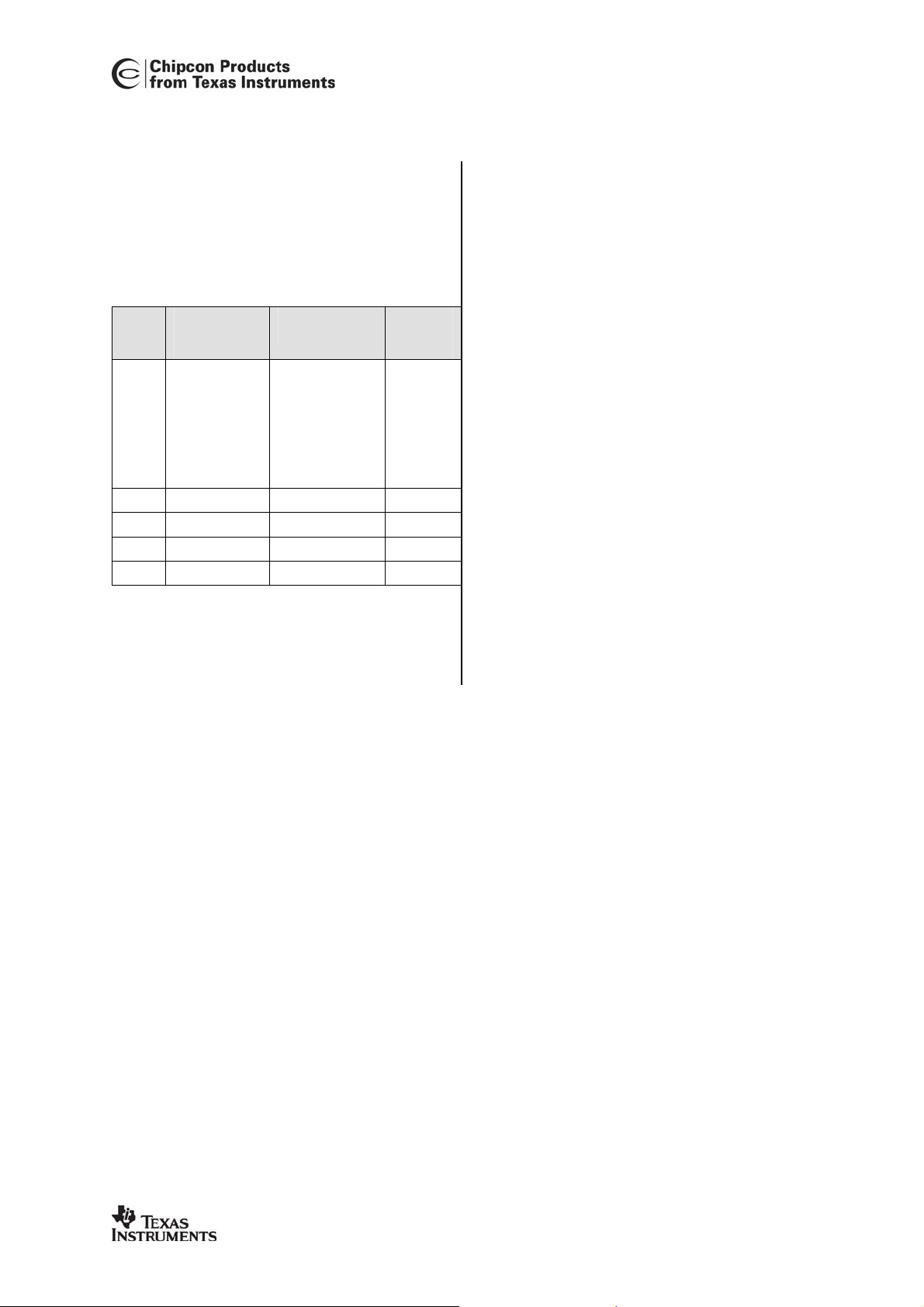
This device is not yet released to market. Volume shipments possible under waiver.
CC2430
Component Description
C191, C211 32 MHz crystal load capacitor 22 pF, 5%, NP0, 0402 22 pF, 5%, NP0, 0402
C241, C421 Load capacitance for power supply
voltage regulators
C341 DC block to antenna and match 5.6 pF, +/- 0.25pF, NP0,
C431, C441 32.768 kHz crystal load capacitor (if low-
frequency crystal is needed in application)
L321 Discrete balun and match 6.8 nH5,, 5%,
L331 Discrete balun and match 22 nH, 5%,
L341 Discrete balun and match 1.8 nH, 5%,
R221 Precision resistor for current reference
generator to system-on-chip part
R261 Precision resistor for current reference
generator to RF part
R451 Pull-up resistor connected to 2.0V-3.6V
power supply.
XTAL1 32 MHz Crystal 32 MHz crystal,
XTAL2 Optional 32.768 kHz watch crystal (if low-
frequency crystal is needed in application)
Single Ended 50Ω Output
220 nF, 10%, 0402 220 nF, 10%, 0402
0402
15 pF, 5%, NP0, 0402 15 pF, 5%, NP0, 0402
Monolithic/multilayer, 0402
Monolithic/multilayer, 0402
Monolithic/multilayer, 0402
56 kΩ, 1%, 0402 56 kΩ, 1%, 0402
43 kΩ, 1%, 0402 43 kΩ, 1%, 0402
ESR < 60 Ω
32.768 kHz crystal,
Epson MC 306.
Differential Antenna
Not used
12 nH 5%,
Monolithic/multilayer, 0402
27 nH, 5%,
Monolithic/multilayer, 0402
Not used
32 MHz crystal,
ESR < 60 Ω
32.768 kHz crystal,
Epson MC 306.
Table 24: Overview of external components (excluding supply decoupling capacitors)
5
For devices with Chip Version register, CHVER.VERSION equal 0x03 or greater
CC2430 PRELIMINARY Data Sheet (rev. 2.01) SWRS036E Page 32 of 233

12 8051 CPU
This device is not yet released to market. Volume shipments possible under waiver.
CC2430
This section describes the 8051 CPU core,
with interrupts, memory and instruction set.
12.1 8051 CPU Introduction
CC2430
The
is an enhanced version of the industry
standard 8051 core.
The enhanced 8051 core uses the standard
8051 instruction set. Instructions execute
faster than the standard 8051 due to the
following:
• One clock per instruction cycle is used
• Wasted bus states are eliminated.
Since an instruction cycle is aligned with
memory fetch when possible, most of the
single byte instructions are performed in a
single clock cycle. In addition to the speed
improvement, the enhanced 8051 core also
includes architectural enhancements:
• A second data pointer.
• Extended 18-source interrupt unit
The 8051 core is object code compatible with
the industry standard 8051 microcontroller.
That is, object code compiled with an industry
standard 8051 compiler or assembler executes
on the 8051 core and is functionally
equivalent. However, because the 8051 core
uses a different instruction timing than many
other 8051 variants, existing code with timing
loops may require modification. Also because
the peripheral units such as timers and serial
ports differ from those on a other 8051 cores,
code which includes instructions using the
peripheral units SFRs will not work correctly.
12.2 Reset
The
following events generate a reset:
• Forcing RESET_N input pin low
• A power-on reset condition
• Watchdog timer reset condition
The initial conditions after a reset are as
follows:
• I/O pins are configured as inputs with
includes an 8-bit CPU core which
as opposed to 12 clocks per
instruction cycle in the standard 8051.
CC2430
has three reset sources. The
pull-up
CC2430 PRELIMINARY Data Sheet (rev. 2.01) SWRS036E Page 33 of 233
• CPU program counter is loaded with
0x0000 and program execution starts
at this address
• All peripheral registers are initialized to
their reset values (refer to register
descriptions)
• Watchdog timer is disabled
12.3 Memory
The 8051 CPU architecture has four different
memory spaces. The 8051 has separate
memory spaces for program memory and data
memory. The 8051 memory spaces are the
following:
CODE. A read-only memory space for
program memory. This memory space can be
up to 64 KB in size.
DATA. A read/write data memory space,
which can be directly or indirectly accessed by
a single cycle CPU instruction, thus allowing
fast access. This memory space can be up to
256 bytes. The lower 128 bytes of the DATA
memory space can be addressed either
directly or indirectly, the upper 128 bytes only
indirectly.
XDATA. A read/write data memory space
access to which usually requires 4-5 CPU
instruction cycles, thus giving slow access.
This memory space can be up to 64 KB in
size. Access to XDATA memory is also slower
in hardware than DATA access as the CODE
and XDATA memory spaces share a common
bus on the CPU core and instruction pre-fetch
from CODE can thus not be performed in
parallel with XDATA accesses.
SFR. A read/write register memory space
which can be directly accessed by a single
CPU instruction. This memory space consists
of 128 bytes. For SFR registers whose
address is divisible by eight, each bit is also
individually addressable.
The four different memory spaces are distinct
in the 8051 architecture, but are partly
overlapping in the
transfers and hardware debugger operation.
How the different memory spaces are mapped
onto the three physical memories (flash
program memory, 8 KB SRAM and memorymapped registers) is described in sections
12.3.1 and 12.3.2.
CC2430
to ease DMA

12.3.1 Memory Map
This device is not yet released to market. Volume shipments possible under waiver.
CC2430
This section gives an overview of the memory
map.
The memory map differs from the standard
8051 memory map in two important aspects,
as described below.
First, in order to allow the DMA controller
access to all physical memory and thus allow
DMA transfers between the different 8051
memory spaces, parts of SFR and CODE
memory space is mapped into the XDATA
memory space.
Secondly, two alternative schemes for CODE
memory space mapping can be used. The first
scheme is the standard 8051 mapping where
only the program memory i.e. flash memory is
mapped to CODE memory space. This
mapping is the default used after a device
reset.
The second scheme is an extension to the
standard CODE space mapping in that all
physical memory is mapped to CODE space,
by using a unified mapping of the CODE
memory space.
Details about mapping of all 8051 memory
spaces are given in the next section.
The memory map showing how the different
physical memories are mapped into the CPU
memory spaces is given in the figures on the
following pages for each flash memory size
option.
Note that for CODE memory space, the two
alternative memory maps are shown; unified
and non-unified (standard) mapping.
For users familiar with the 8051 architecture,
the standard 8051 memory space is shown as
“8051 memory spaces” in the figures.
CC2430 PRELIMINARY Data Sheet (rev. 2.01) SWRS036E Page 34 of 233

This device is not yet released to market. Volume shipments possible under waiver.
CC2430
0xFF
0x00
0xFF
0x80
0xFFFF
XDATA memory space
0x0000
8051 memory spaces
DATA
memory space
R
S
F
e
m
o
m
y
r
0xFFFF
0xFF00
s
p
a
e
c
0xE000
0xDFFF
0xDF80
0xDF00
0xDEFF
0x8000
0x7FFF
0x0000
Fast access RAM
Slow access RAM /
program memory in RAM
Registers
Unimplemented
23 KB
Non-volatile program m emory
32 KB
CC2430-F32
XDATA memory space
8 KB SRAM
SFR registers
RF registers
0x7FFF
32 KB Flash
0x0000
Physical memory
Figure 7: CC2430-F32 XDATA memory space
CC2430 PRELIMINARY Data Sheet (rev. 2.01) SWRS036E Page 35 of 233

This device is not yet released to market. Volume shipments possible under waiver.
CC2430
0xFFFF
Code memory space
0x0000
8051 memory spaces
0xFFFF
Unimplemented
32 KB
0x8000
0x7FFF
Non-volatile program memory
32 KB
0x0000
CC2430-F32 CODE memory space
MEMCTR.MUNIF = 0
CODE maps to flash
memory only
0x7FFF
0x0000
Physical memory
Figure 8: CC2430-F32 Non-unified mapping of CODE Space
32 KB flash
0xFFFF
0xFF00
Fast access RAM
Slow access RAM /
program memory in RAM
0xE000
0xDFFF
0xDF80
0xDF00
0xDEFF
0xDEFF
Registers
Unimplemented
23 KB
0x8000
0x7FFF
Non-volatile program memory
32 KB
0x0000
CC2430-F32 CODE memory space
MEMCTR.MUNIF = 1
CODE maps to unified memory
Figure 9: CC2430-F32 Unified mapping of CODE space
8 KB SRAM
SFR registers
RF registers
0x7FFF
32 KB Flash
0x0000
Physical memory
CC2430 PRELIMINARY Data Sheet (rev. 2.01) SWRS036E Page 36 of 233

This device is not yet released to market. Volume shipments possible under waiver.
CC2430
0xFF
0x00
0xFF
0x80
0xFFFF
XDATA memory space
0x0000
8051 memory spaces
DATA
memory space
R
S
F
m
e
m
o
y
r
0xFFFF
0xFF00
0xEEFF
s
p
a
c
e
0xE000
0xDFFF
0xDF80
0xDF00
0xDEFF
0x0000
Fast access RAM
Slow access RAM /
program memory in RAM
Registers
Non-volatile program memory
55 KB
CC2430-F64 XDATA memory
space
8 KB SRAM
SFR registers
RF registers
0xFFFF
0xDEFF
0x0000
64 KB Flash
lower 55 KB
Physical memory
Figure 10: CC2430-F64 XDATA memory space
CC2430 PRELIMINARY Data Sheet (rev. 2.01) SWRS036E Page 37 of 233

0xFFFF
This device is not yet released to market. Volume shipments possible under waiver.
0xFFFF
CC2430
64 KB flash
0xFFFF
Code memory space
0x0000
8051 memory spaces
0xFFFF
0xFF00
Non-volatile program memory
0x0000
CC2430-F64 CODE memory space
MEMCTR.MUNIF = 0
CODE maps to flash
64 KB
0x0000
memory only
Figure 11: CC2430-F64 Non-unified mapping of CODE Space
Fast access RAM
8 KB SRAM
Physical memory
Slow access RAM /
program memory in RAM
0xE000
0xDFFF
0xDF80
0xDF00
0xDEFF
Registers
SFR registers
RF registers
64 KB Flash
Non-volatile program memory
55 KB
0xDEFF
lower 55 KB
0x0000
CC2430-F64 CODE memory space
0x0000
Physical memory
MEMCTR.MUNIF = 1
CODE maps to unified memory
Figure 12: CC2430-F64 Unified mapping of CODE space
CC2430 PRELIMINARY Data Sheet (rev. 2.01) SWRS036E Page 38 of 233

This device is not yet released to market. Volume shipments possible under waiver.
h
CC2430
0xFF
0x00
0xFF
0x80
0xFFFF
DATA
memory space
S
R
F
m
e
m
o
y
r
XDATA memory space
0x0000
8051 memory spaces
0xFFFF
0xFF00
0xEEFF
Fast access RAM
Slow access RAM /
8 KB SRAM
program memory in RAM
s
p
e
a
c
0xE000
0xDFFF
0xDF80
0xDF00
0xDEFF
Registers
SFR registers
RF registers
0xFFFF
Non-volatile program memory
55 KB
0xDF00
0xDEFF
128 KB Flas
lower 55 KB
0x0000
CC2430-F128 XDATA memory
0x0000
Physical memory
space
Figure 13: CC2430-F128 XDATA memory space
CC2430 PRELIMINARY Data Sheet (rev. 2.01) SWRS036E Page 39 of 233

0xFFFF
Code memory space
0x0000
8051 memory spaces
This device is not yet released to market. Volume shipments possible under waiver.
0xFFFF
Non-volatile program memory
0x8000
0x7FFF
Non-volatile program memory
0x0000
CC2430-F128 CODE memory space
32 KB
bank 0 - bank 3
32 KB
bank 0
CC2430
128 KB flash
0x1FFFF
32 KB
bank 3
0x18000
0x17FFF
32 KB
bank 2
0x10000
0xFFFF
32 KB
bank 1
0x8000
0x7FFF
32 KB
bank 0
0x0000
Physical memory
MEMCTR.MUNIF = 0
CODE maps to flash
memory only
Figure 14: CC2430-F128 Non-unified mapping of CODE Space
0xFFFF
0xFF00
0xE000
0xDFFF
0xDF80
0xDF00
0xDEFF
0x8000
0x7FFF
0x0000
CC2430-F128 CODE memory space
Fast access RAM
Slow access RAM /
program memory in RAM
Registers
Non-volatile program memory
23 KB
bank 0 - bank 3
Non-volatile program memory
32 KB
bank 0
8 KB SRAM
SFR registers
RF registers
128 KB Flash
0x8000 * bank +1 - 0x20FF
23 KB
bank 0-3
0x8000 * bank
0x7FFF
32 KB
bank 0
0x0000
Physical memory
MEMCTR.MUNIF = 1
CODE maps to unified memory
Figure 15: CC2430-F128 Unified mapping of CODE space
CC2430 PRELIMINARY Data Sheet (rev. 2.01) SWRS036E Page 40 of 233

12.3.2 Memory Space
This device is not yet released to market. Volume shipments possible under waiver.
CC2430
This section describes the details of each CPU
memory space.
XDATA memory space
map is given for each flash memory option in
Figure 7, Figure 10 and Figure 13. For the
devices with flash size above 32 KB, the lower
55 KB of the flash program memory is mapped
into the address range 0x0000-0xDEFF. For
the 32 KB flash size option, the 32 KB flash
memory is mapped to 0x0000-0x7FFF in
XDATA memory space.
Access to unimplemented areas shown as
shaded in the memory map gives an
undefined result.
For all device flash-options, the 8 KB SRAM is
mapped into address range 0xE000-0xFFFF.
Also the SFR registers are mapped into
address range 0xDF80-0xDFFF.
Another memory-mapped register area is the
RF register area which is mapped into the
address range 0xDF00-0xDF7F. These
registers are associated with the radio (see
sections 14 and 14.35).
The mapping of flash memory, SRAM and
registers to XDATA allows the DMA controller
and the CPU access to all the physical
memories in a single unified address space.
One of the ramifications of this mapping is that
the first address of usable SRAM starts at
address 0xE000 instead of 0x0000, and
therefore compilers/assemblers must take this
into consideration.
In low-power modes PM2-3, with the lowest
power consumption, the upper 4 KB of SRAM
i.e. the memory locations in XDATA address
range 0xF000-0xFFFF will retain their
contents. There are some locations in this area
that are excepted from retention. Refer to
section 13.10 on page 135 for a detailed
description of power modes and SRAM data
retention.
CODE memory space
space uses either a unified or non-unified
mapping (see section 12.3.1 on page 34) to
the physical memories as shown in Figure 8 Figure 9, Figure 11 - Figure 12 and Figure 14Figure 15. The unified mapping of the CODE
memory space is similar to the XDATA
mapping. Note that some SFR registers
internal to the CPU can not be accessed in the
. The XDATA memory
. The CODE memory
unified CODE memory space (see section
12.4 on page 44).
With flash memory sizes above 32 KB, the
lower 55 KB of flash memory is mapped to
CODE memory space when unified mapping is
used. This is similar to the XDATA memory
space.
The 8 KB SRAM is included in the CODE
address space to allow program execution out
of the SRAM.
Note: in order to use the unified memory
mapping within CODE memory space, the
SFR register bit MEMCTR.MUNIF must be 1.
For devices with flash memory size of 128 KB
(CC2430-F128), a flash memory banking
scheme is used for the CODE memory space.
Since the physical flash memory size is 128
KB, the upper 32 KB area of CODE memory
space is mapped to one out of the four 32 KB
physical banks of flash memory through the
flash bank select bits as shown in the nonunified CODE memory map. The flash bank
select bits reside in the SFR register bits
MEMCTR.FMAP (see section 12.12 on page
68). When unified CODE memory space
mapping is used, the CODE memory is
mapped to the flash memory in a similar
manner to non-unified mapping, using memory
banking, however 23 KB of the selected bank
is available, as shown in the memory map.
Access to unimplemented areas shown as
shaded in the memory map gives an
undefined result.
DATA memory space
range of DATA memory is mapped into the
upper 256 bytes of the 8 KB SRAM. This area
is also accessible through the unified CODE
and XDATA memory spaces at the address
range 0xFF00-0xFFFF.
SFR memory space
register area is accessed through this memory
space. The SFR registers are also accessible
through the XDATA/DMA address space at the
address range 0xDF80-0xDFFF. Some CPUspecific SFR registers reside inside the CPU
core and can only be accessed using the SFR
memory space and not through the duplicate
mapping into XDATA memory space. These
specific SFR registers are listed in section 12.4
on page 44.
. The 8-bit address
. The 128 entry hardware
CC2430 PRELIMINARY Data Sheet (rev. 2.01) SWRS036E Page 41 of 233

This device is not yet released to market. Volume shipments possible under waiver.
CC2430
12.3.3 Data Pointers
The
CC2430
has two data pointers, DPTR0
and DPTR1 to accelerate the movement of
data blocks to/from memory. The data pointers
are generally used to access CODE or XDATA
space e.g.
MOVC A,@A+DPTR
The data pointer select bit, bit 0 in the Data
Pointer Select register DPS, chooses which
data pointer shall be the active one during
execution of an instruction that uses the data
pointer, e.g. in one of the above instructions.
The data pointers are two bytes wide
consisting of the following SFRs:
• DPTR0 – DPH0:DPL0
MOV A,@DPTR
.
• DPTR1 – DPH1:DPL1
DPH0 (0x83) – Data Pointer 0 High Byte
Bit Name Reset R/W Description
7:0
DPH0[7:0]
0 R/W Data pointer 0, high byte
DPL0 (0x82) – Data Pointer 0 Low Byte
Bit Name Reset R/W Description
7:0
DPL0[7:0]
0 R/W Data pointer 0, low byte
DPH1 (0x85) – Data Pointer 1 High Byte
Bit Name Reset R/W Description
7:0
DPH1[7:0]
0 R/W Data pointer 1, high byte
DPL1 (0x84) – Data Pointer 1 Low Byte
Bit Name Reset R/W Description
7:0
DPL1[7:0]
0 R/W Data pointer 1, low byte
DPS (0x92) – Data Pointer Select
Bit Name Reset R/W Description
7:1
0
DPS
0x00 R0 Not used
0 R/W Data pointer select. Selects active data pointer.
0 : DPTR0
1 : DPTR1
12.3.4 XDATA Memory Access
The
CC2430
provides an additional SFR
register MPAGE. This register is used during
instructions
MOVX A,@Ri
and
MOVX @Ri,A.
In some 8051 implementations, this type of
XDATA access is performed using P2 to give
the most significant address bits. Existing
software may therefore have to be adapted to
make use of MPAGE instead of P2.
MPAGE gives the 8 most significant address
bits, while the register Ri gives the 8 least
significant bits.
MPAGE (0x93) – Memory Page Select
Bit Name Reset R/W Description
CC2430 PRELIMINARY Data Sheet (rev. 2.01) SWRS036E Page 42 of 233

This device is not yet released to market. Volume shipments possible under waiver.
Bit Name Reset R/W Description
7:0
MPAGE[7:0]
0x00 R/W
Memory page, high-order bits of address in
instruction
CC2430
MOVX
CC2430 PRELIMINARY Data Sheet (rev. 2.01) SWRS036E Page 43 of 233

This device is not yet released to market. Volume shipments possible under waiver.
Note : all internal SFRs (shown with grey
12.4 SFR Registers
The Special Function Registers (SFRs) control
several of the features of the 8051 CPU core
and/or peripherals. Many of the 8051 core
SFRs are identical to the standard 8051 SFRs.
However, there are additional SFRs that
control features that are not available in the
standard 8051. The additional SFRs are used
to interface with the peripheral units and RF
transceiver.
Table 25 shows the address to all SFRs in
CC2430
. The 8051 internal SFRs are shown
with grey background, while the other SFRs
are the SFRs specific to
CC2430
.
8 bytes
80 P0 SP DPL0 DPH0 DPL1 DPH1 U0CSR PCON 87
88 TCON P0IFG P1IFG P2IFG PICTL P1IEN - P0INP 8F
90 P1 RFIM DPS MPAGE T2CMP ST0 ST1 ST2 97
98 S0CON - IEN2 S1CON T2PEROF0 T2PEROF1 T2PEROF2 FMAP 9F
A0 P2 T2OF0 T2OF1 T2OF2 T2CAPLPL T2CAPHPH T2TLD T2THD A7
A8 IEN0 IP0 - FWT FADDRL FADDRH FCTL FWDATA AF
B0 - ENCDI ENCDO ENCCS ADCCON1 ADCCON2 ADCCON3 - B7
B8 IEN1 IP1 ADCL ADCH RNDL RNDH SLEEP - BF
C0 IRCON U0DBUF U0BAUD T2CNF U0UCR U0GCR CLKCON MEMCTR C7
C8 - WDCTL T3CNT T3CTL T3CCTL0 T3CC0 T3CCTL1 T3CC1 CF
D0 PSW DMAIRQ DMA1CFGL DMA1CFGH DMA0CFGL DMA0CFGH DMAARM DMAREQ D7
D8 TIMIF RFD T1CC0L T1CC0H T1CC1L T1CC1H T1CC2L T1CC2H DF
E0 ACC RFST T1CNTL T1CNTH T1CTL T1CCTL0 T1CCTL1 T1CCTL2 E7
E8 IRCON2 RFIF T4CNT T4CTL T4CCTL0 T4CC0 T4CCTL1 T4CC1 EF
F0 B PERCFG ADCCFG P0SEL P1SEL P2SEL P1INP P2INP F7
F8 U1CSR U1DBUF U1BAUD U1UCR U1GCR P0DIR P1DIR P2DIR FF
background in Table 25), can only be
accessed through SFR space as these
registers are not mapped into XDATA space.
Table 26 lists the additional SFRs that are not
standard 8051 peripheral SFRs or CPUinternal SFRs. The additional SFRs are
described in the relevant sections for each
peripheral function.
CC2430
Table 25: SFR address overview
Table 26: CC2430 specific SFR overview
Register name SFR
Address
ADCCON1 0xB4 ADC ADC Control 1
ADCCON2 0xB5 ADC ADC Control 2
ADCCON3 0xB6 ADC ADC Control 3
ADCL 0xBA ADC ADC Data Low
ADCH 0xBB ADC ADC Data High
RNDL 0xBC ADC Random Number Generator Data Low
Module Description
CC2430 PRELIMINARY Data Sheet (rev. 2.01) SWRS036E Page 44 of 233

This device is not yet released to market. Volume shipments possible under waiver.
CC2430
Register name SFR
Address
RNDH 0xBD ADC Random Number Generator Data High
ENCDI 0xB1 AES Encryption/Decryption Input Data
ENCDO 0xB2 AES Encryption/Decryption Output Data
ENCCS 0xB3 AES Encryption/Decryption Control and Status
DMAIRQ 0xD1 DMA DMA Interrupt Flag
DMA1CFGL 0xD2 DMA DMA Channel 1-4 Configuration Address Low
DMA1CFGH 0xD3 DMA DMA Channel 1-4 Configuration Address High
DMA0CFGL 0xD4 DMA DMA Channel 0 Configuration Address Low
DMA0CFGH 0xD5 DMA DMA Channel 0 Configuration Address High
DMAARM 0xD6 DMA DMA Channel Armed
DMAREQ 0xD7 DMA DMA Channel Start Request and Status
FWT 0xAB FLASH Flash Write Timing
FADDRL 0xAC FLASH Flash Address Low
FADDRH 0xAD FLASH Flash Address High
FCTL 0xAE FLASH Flash Control
FWDATA 0xAF FLASH Flash Write Data
P0IFG 0x89 IOC Port 0 Interrupt Status Flag
P1IFG 0x8A IOC Port 1 Interrupt Status Flag
P2IFG 0x8B IOC Port 2 Interrupt Status Flag
PICTL 0x8C IOC Port Pins Interrupt Mask and Edge
P1IEN 0x8D IOC Port 1 Interrupt Mask
P0INP 0x8F IOC Port 0 Input Mode
PERCFG 0xF1 IOC Peripheral I/O Control
ADCCFG 0xF2 IOC ADC Input Configuration
P0SEL 0xF3 IOC Port 0 Function Select
P1SEL 0xF4 IOC Port 1 Function Select
P2SEL 0xF5 IOC Port 2 Function Select
P1INP 0xF6 IOC Port 1 Input Mode
P2INP 0xF7 IOC Port 2 Input Mode
P0DIR 0xFD IOC Port 0 Direction
P1DIR 0xFE IOC Port 1 Direction
P2DIR 0xFF IOC Port 2 Direction
MEMCTR 0xC7 MEMORY Memory System Control
FMAP 0x9F MEMORY Flash Memory Bank Mapping
RFIM 0x91 RF RF Interrupt Mask
RFD 0xD9 RF RF Data
RFST 0xE1 RF RF Command Strobe
RFIF 0xE9 RF RF Interrupt flags
ST0 0x95 ST Sleep Timer 0
ST1 0x96 ST Sleep Timer 1
ST2 0x97 ST Sleep Timer 2
SLEEP 0xBE PMC Sleep Mode Control
Module Description
CC2430 PRELIMINARY Data Sheet (rev. 2.01) SWRS036E Page 45 of 233

This device is not yet released to market. Volume shipments possible under waiver.
CC2430
Register name SFR
Address
CLKCON 0xC6 PMC Clock Control
T1CC0L 0xDA Timer1 Timer 1 Channel 0 Capture/Compare Value Low
T1CC0H 0xDB Timer1 Timer 1 Channel 0 Capture/Compare Value High
T1CC1L 0xDC Timer1 Timer 1 Channel 1 Capture/Compare Value Low
T1CC1H 0xDD Timer1 Timer 1 Channel 1 Capture/Compare Value High
T1CC2L 0xDE Timer1 Timer 1 Channel 2 Capture/Compare Value Low
T1CC2H 0xDF Timer1 Timer 1 Channel 2 Capture/Compare Value High
T1CNTL 0xE2 Timer1 Timer 1 Counter Low
T1CNTH 0xE3 Timer1 Timer 1 Counter High
T1CTL 0xE4 Timer1 Timer 1 Control and Status
T1CCTL0 0xE5 Timer1 Timer 1 Channel 0 Capture/Compare Control
T1CCTL1 0xE6 Timer1 Timer 1 Channel 1 Capture/Compare Control
T1CCTL2 0xE7 Timer1 Timer 1 Channel 2 Capture/Compare Control
T2CMP 0x94 Timer2 Timer 2 Compare Value
T2PEROF0 0x9C Timer2 Timer 2 Overflow Capture/Compare 0
T2PEROF1 0x9D Timer2 Timer 2 Overflow Capture/Compare 1
T2PEROF2 0x9E Timer2 Timer 2 Overflow Capture/Compare 2
T2OF0 0xA1 Timer2 Timer 2 Overflow Count 0
T2OF1 0xA2 Timer2 Timer 2 Overflow Count 1
T2OF2 0xA3 Timer2 Timer 2 Overflow Count 2
T2CAPLPL 0xA4 Timer2 Timer 2 Timer Period Low
T2CAPHPH 0xA5 Timer2 Timer 2 Timer Period High
T2TLD 0xA6 Timer2 Timer 2 Timer Value Low
T2THD 0xA7 Timer2 Timer 2 Timer Value High
T2CNF 0xC3 Timer2 Timer 2 Configuration
T3CNT 0xCA Timer3 Timer 3 Counter
T3CTL 0xCB Timer3 Timer 3 Control
T3CCTL0 0xCC Timer3 Timer 3 Channel 0 Compare Control
T3CC0 0xCD Timer3 Timer 3 Channel 0 Compare Value
T3CCTL1 0xCE Timer3 Timer 3 Channel 1Compare Control
T3CC1 0xCF Timer3 Timer 3 Channel 1 Compare Value
T4CNT 0xEA Timer4 Timer 4 Counter
T4CTL 0xEB Timer4 Timer 4 Control
T4CCTL0 0xEC Timer4 Timer 4 Channel 0 Compare Control
T4CC0 0xED Timer4 Timer 4 Channel 0 Compare Value
T4CCTL1 0xEE Timer4 Timer 4 Channel 1 Compare Control
T4CC1 0xEF Timer4 Timer 4 Channel 1 Compare Value
TIMIF 0xD8 TMINT Timers 1/3/4 Joint Interrupt Mask/Flags
U0CSR 0x86 USART0 USART 0 Control and Status
U0DBUF 0xC1 USART0 USART 0 Receive/Transmit Data Buffer
U0BAUD 0xC2 USART0 USART 0 Baud Rate Control
U0UCR 0xC4 USART0 USART 0 UART Control
Module Description
CC2430 PRELIMINARY Data Sheet (rev. 2.01) SWRS036E Page 46 of 233

This device is not yet released to market. Volume shipments possible under waiver.
CC2430
Register name SFR
U0GCR 0xC5 USART0 USART 0 Generic Control
U1CSR 0xF8 USART1 USART 1 Control and Status
U1DBUF 0xF9 USART1 USART 1 Receive/Transmit Data Buffer
U1BAUD 0xFA USART1 USART 1 Baud Rate Control
U1UCR 0xFB USART1 USART 1 UART Control
U1GCR 0xFC USART1 USART 1 Generic Control
WDCTL 0xC9 WDT Watchdog Timer Control
12.5 CPU Registers
This section describes the internal registers
found in the CPU.
12.5.1 Registers R0-R7
CC2430
The
eight registers each. These register banks are
mapped in the DATA memory space at
addresses 0x00-0x07, 0x08-0x0F, 0x10-0x17
and 0x18-0x1F. Each register bank contains
the eight 8-bit register R0-R7. The register
bank to be used is selected through the
Program Status Word PSW.RS[1:0].
Address
provides four register banks of
Module Description
12.5.2 Program Status Word
The Program Status Word (PSW) contains
several bits that show the current state of the
CPU. The Program Status Word is accessible
as an SFR and it is bit-addressable. PSW is
shown below and contains the Carry flag,
Auxiliary Carry flag for BCD operations,
Register Select bits, Overflow flag and Parity
flag. Two bits in PSW are uncommitted and can
be used as user-defined status flags
.
CC2430 PRELIMINARY Data Sheet (rev. 2.01) SWRS036E Page 47 of 233

This device is not yet released to market. Volume shipments possible under waiver.
PSW (0xD0) – Program Status Word
Bit Name Reset R/W Description
7
6
5
4:3
2
1
0
CY
AC
F0
RS[1:0]
OV
F1
P
0 R/W Carry flag. Set to 1 when the last arithmetic operation
0 R/W Auxiliary carry flag for BCD operations. Set to 1 when the
0 R/W User-defined, bit-addressable
00 R/W
0 R/W Overflow flag, set by arithmetic operations. Set to 1 when
0 R/W User-defined, bit-addressable
0 R/W Parity flag, parity of accumulator set by hardware to 1 if it
resulted in a carry (during addition) or borrow (during
subtraction), otherwise cleared to 0 by all arithmetic
operations.
last arithmetic operation resulted in a carry into (during
addition) or borrow from (during subtraction) the high order
nibble, otherwise cleared to 0 by all arithmetic operations.
Register bank select bits. Selects which set of R7-R0
registers to use from four possible register banks in DATA
space.
00 Bank 0, 0x00 – 0x07
01 Bank 1, 0x08 – 0x0F
10 Bank 2, 0x10 – 0x17
11 Bank 3, 0x18 – 0x1F
the last arithmetic operation resulted in a carry (addition),
borrow (subtraction), or overflow (multiply or divide).
Otherwise, the bit is cleared to 0 by all arithmetic
operations.
contains an odd number of 1’s, otherwise it is cleared to 0
CC2430
12.5.3 Accumulator
ACC is the accumulator. This is the source
and destination of most arithmetic instructions,
data transfers and other instructions. The
mnemonic for the accumulator (in instructions
involving the accumulator) refers to A instead
of ACC.
ACC (0xE0) – Accumulator
Bit Name Reset R/W Description
7:0
ACC[7:0]
0x00 R/W Accumulator
12.5.4 B Register
The B register is used as the second 8-bit
divide instructions. When not used for these
purposes it may be used as a scratch-pad
register to hold temporary data.
argument during execution of multiply and
B (0xF0) – B Register
Bit Name Reset R/W Description
7:0
B[7:0]
0x00 R/W
B register. Used in
MUL/DIV
instructions.
CC2430 PRELIMINARY Data Sheet (rev. 2.01) SWRS036E Page 48 of 233

This device is not yet released to market. Volume shipments possible under waiver.
CC2430
12.5.5 Stack Pointer
The stack resides in DATA memory space and
grows upwards. The
increments the Stack Pointer (SP) and then
copies the byte into the stack. The Stack
Pointer is initialized to 0x07 after a reset and it
SP (0x81) – Stack Pointer
Bit Name Reset R/W Description
7:0
SP[7:0]
12.6 Instruction Set Summary
The 8051 instruction set is summarized in
Table 27. All mnemonics copyrighted © Intel
Corporation, 1980.
The following conventions are used in the
instruction set summary:
• Rn – Register R7-R0 of the currently
selected register bank.
• direct – 8-bit internal data location’s
address. This can be DATA area (0x00 –
0x7F) or SFR area (0x80 – 0xFF).
• @Ri – 8-bit internal data location, DATA
area (0x00 – 0xFF) addressed indirectly
through register R1 or R0.
• #data – 8-bit constant included in
instruction.
• #data16 – 16-bit constant included in
instruction.
PUSH
instruction first
0x07 R/W Stack Pointer
is incremented once to start from location 0x08
which is the first register (R0) of the second
register bank. Thus, in order to use more than
one register bank, the SP should be initialized
to a different location not used for data
storage.
• addr16 – 16-bit destination address. Used
• addr11 – 11-bit destination address. Used
• rel – Signed (two’s complement) 8-bit
• bit – direct addressed bit in DATA area or
The instructions that affect CPU flag settings
located in PSW are listed in Table 28 on page
53. Note that operations on the PSW register or
bits in PSW will also affect the flag settings.
LCALL
ACALL
and
and
by
anywhere within the 64 KB CODE memory
space.
by
within the same 2 KB page of program
memory as the first byte of the following
instruction.
offset byte. Used by
conditional jumps. Range is –128 to +127
bytes relative to first byte of the following
instruction.
SFR.
LJMP
. A branch can be
AJMP
. The branch will be
SJMP
and all
CC2430 PRELIMINARY Data Sheet (rev. 2.01) SWRS036E Page 49 of 233

This device is not yet released to market. Volume shipments possible under waiver.
Table 27: Instruction Set Summary
CC2430
Mnemonic Description Hex
Opcode
Arithmetic operations
ADD A,Rn Add register to accumulator 28-2F 1 1
ADD A,direct Add direct byte to accumulator 25 2 2
ADD A,@Ri Add indirect RAM to accumulator 26-27 1 2
ADD A,#data Add immediate data to accumulator 24 2 2
ADDC A,Rn Add register to accumulator with carry flag 38-3F 1 1
ADDC A,direct Add direct byte to A with carry flag 35 2 2
ADDC A,@Ri Add indirect RAM to A with carry flag 36-37 1 2
ADDC A,#data Add immediate data to A with carry flag 34 2 2
SUBB A,Rn Subtract register from A with borrow 98-9F 1 1
SUBB A,direct Subtract direct byte from A with borrow 95 2 2
SUBB A,@Ri Subtract indirect RAM from A with borrow 96-97 1 2
SUBB A,#data Subtract immediate data from A with borrow 94 2 2
INC A Increment accumulator 04 1 1
INC Rn Increment register 08-0F 1 2
INC direct Increment direct byte 05 2 3
INC @Ri Increment indirect RAM 06-07 1 3
INC DPTR Increment data pointer A3 1 1
DEC A Decrement accumulator 14 1 1
DEC Rn Decrement register 18-1F 1 2
DEC direct Decrement direct byte 15 2 3
DEC @Ri Decrement indirect RAM 16-17 1 3
MUL AB Multiply A and B A4 1 5
DIV Divide A by B 84 1 5
DA A Decimal adjust accumulator D4 1 1
Logical operations
ANL A,Rn AND register to accumulator 58-5F 1 1
ANL A,direct AND direct byte to accumulator 55 2 2
ANL A,@Ri AND indirect RAM to accumulator 56-57 1 2
ANL A,#data AND immediate data to accumulator 54 2 2
ANL direct,A AND accumulator to direct byte 52 2 3
ANL direct,#data AND immediate data to direct byte 53 3 4
ORL A,Rn OR register to accumulator 48-4F 1 1
ORL A,direct OR direct byte to accumulator 45 2 2
ORL A,@Ri OR indirect RAM to accumulator 46-47 1 2
ORL A,#data OR immediate data to accumulator 44 2 2
ORL direct,A OR accumulator to direct byte 42 2 3
ORL direct,#data OR immediate data to direct byte 43 3 4
XRL A,Rn Exclusive OR register to accumulator 68-6F 1 1
XRL A,direct Exclusive OR direct byte to accumulator 65 2 2
Bytes Cycles
CC2430 PRELIMINARY Data Sheet (rev. 2.01) SWRS036E Page 50 of 233

This device is not yet released to market. Volume shipments possible under waiver.
CC2430
Mnemonic Description Hex
Opcode
XRL A,@Ri Exclusive OR indirect RAM to accumulator 66-67 1 2
XRL A,#data Exclusive OR immediate data to accumulator 64 2 2
XRL direct,A Exclusive OR accumulator to direct byte 62 2 3
XRL direct,#data Exclusive OR immediate data to direct byte 63 3 4
CLR A Clear accumulator E4 1 1
CPL A Complement accumulator F4 1 1
RL A Rotate accumulator left 23 1 1
RLC A Rotate accumulator left through carry 33 1 1
RR A Rotate accumulator right 03 1 1
RRC A Rotate accumulator right through carry 13 1 1
SWAP A Swap nibbles within the accumulator C4 1 1
Data transfers
MOV A,Rn Move register to accumulator E8-EF 1 1
MOV A,direct Move direct byte to accumulator E5 2 2
MOV A,@Ri Move indirect RAM to accumulator E6-E7 1 2
MOV A,#data Move immediate data to accumulator 74 2 2
MOV Rn,A Move accumulator to register F8-FF 1 2
MOV Rn,direct Move direct byte to register A8-AF 2 4
MOV Rn,#data Move immediate data to register 78-7F 2 2
MOV direct,A Move accumulator to direct byte F5 2 3
MOV direct,Rn Move register to direct byte 88-8F 2 3
MOV direct1,direct2 Move direct byte to direct byte 85 3 4
MOV direct,@Ri Move indirect RAM to direct byte 86-87 2 4
MOV direct,#data Move immediate data to direct byte 75 3 3
MOV @Ri,A Move accumulator to indirect RAM F6-F7 1 3
MOV @Ri,direct Move direct byte to indirect RAM A6-A7 2 5
MOV @Ri,#data Move immediate data to indirect RAM 76-77 2 3
MOV DPTR,#data16 Load data pointer with a 16-bit constant 90 3 3
MOVC A,@A+DPTR Move code byte relative to DPTR to accumulator 93 1 3
MOVC A,@A+PC Move code byte relative to PC to accumulator 83 1 3
MOVX A,@Ri Move external RAM (8-bit address) to A E2-E3 1 3-10
MOVX A,@DPTR Move external RAM (16-bit address) to A E0 1 3-10
MOVX @Ri,A Move A to external RAM (8-bit address) F2-F3 1 4-11
MOVX @DPTR,A Move A to external RAM (16-bit address) F0 1 4-11
PUSH direct Push direct byte onto stack C0 2 4
POP direct Pop direct byte from stack D0 2 3
XCH A,Rn Exchange register with accumulator C8-CF 1 2
XCH A,direct Exchange direct byte with accumulator C5 2 3
XCH A,@Ri Exchange indirect RAM with accumulator C6-C7 1 3
XCHD A,@Ri Exchange low-order nibble indirect. RAM with A D6-D7 1 3
Program branching
ACALL addr11 Absolute subroutine call xxx11 2 6
Bytes Cycles
CC2430 PRELIMINARY Data Sheet (rev. 2.01) SWRS036E Page 51 of 233

This device is not yet released to market. Volume shipments possible under waiver.
CC2430
Mnemonic Description Hex
Opcode
LCALL addr16 Long subroutine call 12 3 6
RET Return from subroutine 22 1 4
RETI Return from interrupt 32 1 4
AJMP addr11 Absolute jump xxx01 2 3
LJMP addr16 Long jump 02 3 4
SJMP rel Short jump (relative address) 80 2 3
JMP @A+DPTR Jump indirect relative to the DPTR 73 1 2
JZ rel Jump if accumulator is zero 60 2 3
JNZ rel Jump if accumulator is not zero 70 2 3
JC rel Jump if carry flag is set 40 2 3
JNC Jump if carry flag is not set 50 2 3
JB bit,rel Jump if direct bit is set 20 3 4
JNB bit,rel Jump if direct bit is not set 30 3 4
JBC bit,direct rel Jump if direct bit is set and clear bit 10 3 4
CJNE A,direct rel Compare direct byte to A and jump if not equal B5 3 4
CJNE A,#data rel Compare immediate to A and jump if not equal B4 3 4
CJNE Rn,#data rel Compare immediate to reg. and jump if not equal B8-BF 3 4
CJNE @Ri,#data rel Compare immediate to indirect and jump if not equal B6-B7 3 4
DJNZ Rn,rel Decrement register and jump if not zero D8-DF 2 3
DJNZ direct,rel Decrement direct byte and jump if not zero D5 3 4
NOP No operation 00 1 1
Boolean variable operations
CLR C Clear carry flag C3 1 1
CLR bit Clear direct bit C2 2 3
SETB C Set carry flag D3 1 1
SETB bit Set direct bit D2 2 3
CPL C Complement carry flag B3 1 1
CPL bit Complement direct bit B2 2 3
ANL C,bit AND direct bit to carry flag 82 2 2
ANL C,/bit AND complement of direct bit to carry B0 2 2
ORL C,bit OR direct bit to carry flag 72 2 2
ORL C,/bit OR complement of direct bit to carry A0 2 2
MOV C,bit Move direct bit to carry flag A2 2 2
MOV bit,C Move carry flag to direct bit 92 2 3
Bytes Cycles
CC2430 PRELIMINARY Data Sheet (rev. 2.01) SWRS036E Page 52 of 233

This device is not yet released to market. Volume shipments possible under waiver.
Instruction CY OV AC
ADD x x x
ADDC x x x
SUBB x x x
MUL 0 x -
DIV 0 x -
DA x - -
RRC x - -
RLC x - -
SETB C 1 - -
CLR C x - -
CPL C x - -
ANL C,bit x - -
ANL C,/bit x - -
ORL C,bit x - -
ORL C,/bit x - -
MOV C,bit x - -
CJNE x - -
“0”=set to 0, “1”=set to 1, “x”=set to 0/1, “-“=not affected
CC2430
Table 28: Instructions that affect flag settings
12.7 Interrupts
The CPU has 18 interrupt sources. Each
source has its own request flag located in a set
of Interrupt Flag SFR registers. Each interrupt
requested by the corresponding flag can be
individually enabled or disabled. The
definitions of the interrupt sources and the
interrupt vectors are given in Table 29.
The interrupts are grouped into a set of priority
level groups with selectable priority levels.
The interrupt enable registers are described in
section 12.7.1 and the interrupt priority settings
are described in section 12.7.3 on page 61.
12.7.1 Interrupt Masking
Each interrupt can be individually enabled or
disabled by the interrupt enable bits in the
Interrupt Enable SFRs IEN0, IEN1 and IEN2.
The Interrupt Enable SFRs are described
below and summarized in Table 29.
Note that some peripherals have several
events that can generate the interrupt request
associated with that peripheral. This applies to
Port 0, Port 1, Port 2, DMA, Timer 1, Timer2,
Timer 3 , Timer 4 and Radio. These
peripherals have interrupt mask bits for each
internal interrupt source in the corresponding
SFR registers.
In order to use any of the interrupts in the
CC2430
, the following steps must be taken
1. Clear interrupt flags
2. Enable global interrupt by setting the
EA bit in IEN0 to 1
3. Set the corresponding individual,
interrupt enable bit in the IEN0, IEN1
or IEN2 registers to 1.
4. Set individual interrupt enable bit in
the peripherals SFR register, if any.
5. Begin the interrupt service routine at
the corresponding vector address of
that interrupt. See Table 29 for
addresses.
CC2430 PRELIMINARY Data Sheet (rev. 2.01) SWRS036E Page 53 of 233

This device is not yet released to market. Volume shipments possible under waiver.
CC2430
Interrupt
number
0 RF TX FIFO underflow and RX
1 ADC end of conversion ADC 0Bh
2 USART0 RX complete URX0 13h
3 USART1 RX complete URX1 1Bh
4 AES encryption/decryption
5 Sleep Timer compare ST 2Bh
6 Port 2 inputs P2INT 33h
7 USART0 TX complete UTX0 3Bh
8 DMA transfer complete DMA 43h
9 Timer 1 (16-bit)
10 Timer 2 (MAC Timer) T2 53h
11 Timer 3 (8-bit) compare/overflow T3 5Bh
12 Timer 4 (8-bit) compare/overflow T4 63h
13 Port 0 inputs P0INT 6Bh
14 USART1 TX complete UTX1 73h
15 Port 1 inputs P1INT 7Bh
16 RF general interrupts RF 83h
17 Watchdog overflow in timer mode WDT 8Bh
Description Interrupt
FIFO overflow.
complete
capture/compare/overflow
name
RFERR 03h
ENC 23h
T1 4Bh
Interrupt
Vector
Interrupt Mask Interrupt Flag
IEN0.RFERRIE
IEN0.ADCIE
IEN0.URX0IE TCON.URX0IF
IEN0.URX1IE TCON.URX1IF
IEN0.ENCIE S0CON.ENCIF
IEN0.STIE IRCON.STIF
IEN2.P2IE IRCON2.P2IF
IEN2.UTX0IE IRCON2.UTX0IF
IEN1.DMAIE IRCON.DMAIF
IEN1.T1IE IRCON.T1IF
IEN1.T2IE IRCON.T2IF
IEN1.T3IE IRCON.T3IF
IEN1.T4IE IRCON.T4IF
IEN1.P0IE IRCON.P0IF
IEN2.UTX1IE IRCON2.UTX1IF
IEN2.P1IE IRCON2.P1IF
IEN2.RFIE S1CON.RFIF
IEN2.WDTIE IRCON2.WDTIF
TCON.RFERRIF
TCON.ADCIF
Table 29: Interrupts Overview
CC2430 PRELIMINARY Data Sheet (rev. 2.01) SWRS036E Page 54 of 233

This device is not yet released to market. Volume shipments possible under waiver.
IEN0 (0xA8) – Interrupt Enable 0
Bit Name Reset R/W Description
7
6
5
4
3
2
1
0
EA
STIE
ENCIE
URX1IE
URX0IE
ADCIE
RFERRIE
0 R/W
0 R0 Not used. Read as 0
0 R/W
0 R/W
0 R/W
0 R/W
0 R/W
0 R/W
Disables all interrupts.
0 No interrupt will be acknowledged
1 Each interrupt source is individually enabled or disabled by
setting its corresponding enable bit
STIE – Sleep Timer interrupt enable
0 Interrupt disabled
1 Interrupt enabled
ENCIE – AES encryption/decryption interrupt enable
0 Interrupt disabled
1 Interrupt enabled
URX1IE – USART1 RX interrupt enable
0 Interrupt disabled
1 Interrupt enabled
URX0IE - USART0 RX interrupt enable
0 Interrupt disabled
1 Interrupt enabled
ADCIE – ADC interrupt enable
0 Interrupt disabled
1 Interrupt enabled
RFERRIE – RF TX/RX FIFO interrupt enable
0 Interrupt disabled
1 Interrupt enabled
CC2430
CC2430 PRELIMINARY Data Sheet (rev. 2.01) SWRS036E Page 55 of 233

This device is not yet released to market. Volume shipments possible under waiver.
IEN1 (0xB8) – Interrupt Enable 1
Bit Name Reset R/W Description
7:6
5
4
3
2
1
0
P0IE
T4IE
T3IE
T2IE
T1IE
DMAIE
00 R0 Not used. Read as 0
0 R/W
0 R/W
0 R/W
0 R/W
0 R/W
0 R/W
P0IE – Port 0 interrupt enable
0 Interrupt disabled
1 Interrupt enabled
T4IE - Timer 4 interrupt enable
0 Interrupt disabled
1 Interrupt enabled
T3IE - Timer 3 interrupt enable
0 Interrupt disabled
1 Interrupt enabled
T2IE – Timer 2 interrupt enable
0 Interrupt disabled
1 Interrupt enabled
T1IE – Timer 1 interrupt enable
0 Interrupt disabled
1 Interrupt enabled
DMAIE – DMA transfer interrupt enable
0 Interrupt disabled
1 Interrupt enabled
CC2430
CC2430 PRELIMINARY Data Sheet (rev. 2.01) SWRS036E Page 56 of 233

This device is not yet released to market. Volume shipments possible under waiver.
IEN2 (0x9A) – Interrupt Enable 2
Bit Name Reset R/W Description
7:6
5
4
3
2
1
0
WDTIE
P1IE
UTX1IE
UTX0IE
P2IE
RFIE
00 R0 Not used. Read as 0
0 R/W
0 R/W
0 R/W
0 R/W
0 R/W
0 R/W
WDTIE – Watchdog timer interrupt enable
0 Interrupt disabled
1 Interrupt enabled
P1IE– Port 1 interrupt enable
0 Interrupt disabled
1 Interrupt enabled
UTX1IE – USART1 TX interrupt enable
0 Interrupt disabled
1 Interrupt enabled
UTX0IE - USART0 TX interrupt enable
0 Interrupt disabled
1 Interrupt enabled
P2IE – Port 2 interrupt enable
0 Interrupt disabled
1 Interrupt enabled
RFIE – RF general interrupt enable
0 Interrupt disabled
1 Interrupt enabled
CC2430
12.7.2 Interrupt Processing
When an interrupt occurs, the CPU will vector
to the interrupt vector address as shown in
Table 29. Once an interrupt service has
begun, it can be interrupted only by a higher
priority interrupt. The interrupt service is
terminated by a
instruction). When an
RETI
(return from interrupt
RETI
is performed, the
CPU will return to the instruction that would
have been next when the interrupt occurred.
When the interrupt condition occurs, the CPU
will also indicate this by setting an interrupt
flag bit in the interrupt flag registers. This bit is
set regardless of whether the interrupt is
enabled or disabled. If the interrupt is enabled
when an interrupt flag is set, then on the next
instruction cycle the interrupt will be
LCALL
acknowledged by hardware forcing an
to the appropriate vector address.
Interrupt response will require a varying
amount of time depending on the state of the
CPU when the interrupt occurs. If the CPU is
performing an interrupt service with equal or
greater priority, the new interrupt will be
pending until it becomes the interrupt with
highest priority. In other cases, the response
time depends on current instruction. The
fastest possible response to an interrupt is
seven machine cycles. This includes one
machine cycle for detecting the interrupt and
six cycles to perform the
LCALL
.
CC2430 PRELIMINARY Data Sheet (rev. 2.01) SWRS036E Page 57 of 233

This device is not yet released to market. Volume shipments possible under waiver.
TCON (0x88) – Interrupt Flags
Bit Name Reset R/W Description
7
6
5
4
3
2
1
0
URX1IF
ADCIF
URX0IF
IT1
RFERRIF
IT0
0 R/W
H0
0 R/W Not used
0 R/W
H0
0 R/W Not used
0 R/W
H0
1 R/W Reserved. Must always be set to 1.
0 R/W
H0
1 R/W Reserved. Must always be set to 1.
URX1IF – USART1 RX interrupt flag. Set to 1 when USART1 RX
interrupt occurs and cleared when CPU vectors to the interrupt
service routine.
0 Interrupt not pending
1 Interrupt pending
ADCIF – ADC interrupt flag. Set to 1 when ADC interrupt occurs
and cleared when CPU vectors to the interrupt service routine.
0 Interrupt not pending
1 Interrupt pending
URX0IF – USART0 RX interrupt flag. Set to 1 when USART0
interrupt occurs and cleared when CPU vectors to the interrupt
service routine.
0 Interrupt not pending
1 Interrupt pending
RFERRIF – RF TX/RX FIFO interrupt flag. Set to 1 when RFERR
interrupt occurs and cleared when CPU vectors to the interrupt
service routine.
0 Interrupt not pending
1 Interrupt pending
CC2430
CC2430 PRELIMINARY Data Sheet (rev. 2.01) SWRS036E Page 58 of 233

This device is not yet released to market. Volume shipments possible under waiver.
S0CON (0x98) – Interrupt Flags 2
Bit Name Reset R/W Description
7:2
1
0
ENCIF_1
ENCIF_0
0x00 R/W Not used
0 R/W
0 R/W
ENCIF – AES interrupt. ENC has two interrupt flags, ENCIF_1 and
ENCIF_0. Setting one of these flags will request interrupt service.
Both flags are set when the AES co-processor requests the
interrupt.
0 Interrupt not pending
1 Interrupt pending
ENCIF – AES interrupt. ENC has two interrupt flags, ENCIF_1 and
ENCIF_0. Setting one of these flags will request interrupt service.
Both flags are set when the AES co-processor requests the
interrupt.
0 Interrupt not pending
1 Interrupt pending
CC2430
S1CON (0x9B) – Interrupt Flags 3
Bit Name Reset R/W Description
7:2
1
0
RFIF_1
RFIF_0
0x00 R/W Not used
0 R/W
0 R/W
RFIF – RF general interrupt. RF has two interrupt flags, RFIF_1
and RFIF_0. Setting one of these flags will request interrupt
service. Both flags are set when the radio requests the interrupt.
0 Interrupt not pending
1 Interrupt pending
RFIF – RF general interrupt. RF has two interrupt flags, RFIF_1
and RFIF_0. Setting one of these flags will request interrupt
service. Both flags are set when the radio requests the interrupt.
0 Interrupt not pending
1 Interrupt pending
CC2430 PRELIMINARY Data Sheet (rev. 2.01) SWRS036E Page 59 of 233

This device is not yet released to market. Volume shipments possible under waiver.
IRCON (0xC0) – Interrupt Flags 4
Bit Name Reset R/W Description
7
6
5
4
3
2
1
0
STIF
P0IF
T4IF
T3IF
T2IF
T1IF
DMAIF
0 R/W
0 R/W Not used
0 R/W
0 R/W
H0
0 R/W
H0
0 R/W
H0
0 R/W
H0
0 R/W
STIF – Sleep timer interrupt flag
0 Interrupt not pending
1 Interrupt pending
P0IF – Port 0 interrupt flag
0 Interrupt not pending
1 Interrupt pending
T4IF – Timer 4 interrupt flag. Set to 1 when Timer 4 interrupt
occurs and cleared when CPU vectors to the interrupt service
routine.
0 Interrupt not pending
1 Interrupt pending
T3IF – Timer 3 interrupt flag. Set to 1 when Timer 3 interrupt
occurs and cleared when CPU vectors to the interrupt service
routine.
0 Interrupt not pending
1 Interrupt pending
T2IF – Timer 2 interrupt flag. Set to 1 when Timer 2 interrupt
occurs and cleared when CPU vectors to the interrupt service
routine.
0 Interrupt not pending
1 Interrupt pending
T1IF – Timer 1 interrupt flag. Set to 1 when Timer 1 interrupt
occurs and cleared when CPU vectors to the interrupt service
routine.
0 Interrupt not pending
1 Interrupt pending
DMAIF – DMA complete interrupt flag.
0 Interrupt not pending
1 Interrupt pending
CC2430
CC2430 PRELIMINARY Data Sheet (rev. 2.01) SWRS036E Page 60 of 233

This device is not yet released to market. Volume shipments possible under waiver.
IRCON2 (0xE8) – Interrupt Flags 5
Bit Name Reset R/W Description
7:5
4
3
2
1
0
WDTIF
P1IF
UTX1IF
UTX0IF
P2IF
00 R/W Not used
0 R/W
0 R/W
0 R/W
0 R/W
0 R/W
WDTIF – Watchdog timer interrupt flag.
0 Interrupt not pending
1 Interrupt pending
P1IF – Port 1 interrupt flag.
0 Interrupt not pending
1 Interrupt pending
UTX1IF – USART1 TX interrupt flag.
0 Interrupt not pending
1 Interrupt pending
UTX0IF – USART0 TX interrupt flag.
0 Interrupt not pending
1 Interrupt pending
P2IF – Port2 interrupt flag.
0 Interrupt not pending
1 Interrupt pending
CC2430
12.7.3 Interrupt Priority
The interrupts are grouped into six interrupt
priority groups and the priority for each group
is set by the registers IP0 and IP1. In order to
assign a higher priority to an interrupt, i.e. to its
interrupt group, the corresponding bits in IP0
and IP1 must be set as shown in Table 30 on
page 62.
The interrupt priority groups with assigned
interrupt sources are shown in Table 31. Each
group is assigned one of four priority levels.
While an interrupt service request is in
progress, it cannot be interrupted by a lower or
same level interrupt.
In the case when interrupt requests of the
same priority level are received
simultaneously, the polling sequence shown in
Table 32 is used to resolve the priority of each
request.
CC2430 PRELIMINARY Data Sheet (rev. 2.01) SWRS036E Page 61 of 233

This device is not yet released to market. Volume shipments possible under waiver.
IP1 (0xB9) – Interrupt Priority 1
Bit Name Reset R/W Description
7:6
-
5
IP1_5
4
IP1_4
3
IP1_3
2
IP1_2
1
IP1_1
0
IP1_0
12.7.4
IP0 (0xA9) – Interrupt Priority 0
Bit Name Reset R/W Description
7:6
-
5
IP0_5
4
IP0_4
3
IP0_3
2
IP0_2
1
IP0_1
0
IP0_0
00 R/W Not used.
0 R/W Interrupt group 5, priority control bit 1, refer to Table 30
0 R/W Interrupt group 4, priority control bit 1, refer to Table 30
0 R/W Interrupt group 3, priority control bit 1, refer to Table 30
0 R/W Interrupt group 2, priority control bit 1, refer to Table 30
0 R/W Interrupt group 1, priority control bit 1, refer to Table 30
0 R/W Interrupt group 0, priority control bit 1, refer to Table 30
00 R/W Not used.
0 R/W Interrupt group 5, priority control bit 0, refer to Table 30
0 R/W Interrupt group 4, priority control bit 0, refer to Table 30
0 R/W Interrupt group 3, priority control bit 0, refer to Table 30
0 R/W Interrupt group 2, priority control bit 0, refer to Table 30
0 R/W Interrupt group 1, priority control bit 0, refer to Table 30
0 R/W Interrupt group 0, priority control bit 0, refer to Table 30
CC2430
IP1_x IP0_x Priority Level
0 0
0 1
1 0
1 1
0 – lowest
1
2
3 – highest
Table 30: Priority Level Setting
Group Interrupts
IP0 RFERR RF DMA
IP1 ADC P2INT T1
IP2 URX0 UTX0 T2
IP3 URX1 UTX1 T3
IP4 ENC P1INT T4
IP5 ST WDT P0INT
Table 31: Interrupt Priority Groups
CC2430 PRELIMINARY Data Sheet (rev. 2.01) SWRS036E Page 62 of 233

This device is not yet released to market. Volume shipments possible under waiver.
Interrupt number Interrupt name
0 RFERR
16 RF
8 DMA
1 ADC
9 T1
2 URX0
10 T2
3 URX1
11 T3
4 ENC
12 T4
5 ST
13 P0INT
6 P2INT
7 UTX0
14 UTX1
15 P1INT
17 WDT
Polling sequence
CC2430
Table 32: Interrupt Polling Sequence
12.8 Oscillators and clocks
The
CC2430
has one internal system clock.
The source for the system clock can be either
a 16 MHz high-frequency RC oscillator or a 32
MHz crystal oscillator. Clock control is
performed using the CLKCON SFR register
described in section 13.10.
The system clock also feeds all 8051
peripherals (as described in section 6).
The choice of oscillator allows a trade-off
between high-accuracy in the case of the
crystal oscillator and low power consumption
when the high-frequency RC oscillator is used.
Note that operation of the RF transceiver
requires that the crystal oscillator is used.
Optional tuning of the 32 MHz crystal oscillator
load capacitance is supported. In most
applications this is usually not needed. The
tuning functionality is available in RF register
XOSC32M, where a step-wise capacitance
can be added from the XOSC_Q1 and
XOSC_Q2 pins to ground (see Figure 6 on
page 31). Adding more capacitance will lower
the frequency. This can be used to tune away
initial crystal inaccuracy. The oscillator
frequency can be measured during production
and the result can be stored in the internal
flash memory and used on power-up. Some
applications may also use this to compensate
for temperature drift in the crystal, by
measuring the temperature and compensating
accordingly. This must be handled by
software.
By default, no additional capacitance is added
to the oscillator pins. If tuning is necessary, the
external capacitors (C211 and C191 in Figure
6) should be reduced such that the mid-value
of the XOSC32M register corresponds to the
nominal center frequency of the crystal.
CC2430 PRELIMINARY Data Sheet (rev. 2.01) SWRS036E Page 63 of 233

This device is not yet released to market. Volume shipments possible under waiver.
12.9 Debug Interface
The
CC2430
provides a two-wire interface to an on-chip
debug module. The debug interface allows
programming of the on-chip flash and it
provides access to memory and register
contents and debug features such as
breakpoints, single-stepping and register
modification.
includes a debug interface that
CC2430
12.9.2 Debug Communication
The debug interface uses an SPI-like two-wire
interface consisting of the Debug Data (P2_1)
and Debug Clock (P2_2) pins. Data is driven
on the bi-directional Debug Data pin at the
positive edge of Debug Clock and data is
sampled on the negative edge of this clock.
The debug interface uses the I/O pins P2_1 as
Debug Data and P2_2 as Debug Clock during
Debug mode. These I/O pins can be used as
general purpose I/O only while the device is
not in Debug mode. Thus the debug interface
does not interfere with any peripheral I/O pins.
12.9.1 Debug Mode
Debug mode is entered by forcing two rising
edge transitions on pin P2_2 (Debug Clock)
while the RESET_N input is held low. See
section 13.1.6 for pull-up resistor
recommendation for pin P2_2.
While in Debug mode pin P2_1 is the Debug
Data bi-directional pin and P2_2 is the Debug
Clock input pin.
P2_2
P2_1
command first data byte second data byte
Debug commands are sent by an external host
and consist of 1 to 4 output bytes (including
command byte) from the host and an optional
input byte read by the host. Command and
data is transferred with MSB first. Figure 16
shows a timing diagram of data on the debug
interface.
The first byte of the debug command is a
command byte and is encoded as follows:
• bits 7 to 3 : instruction code
• bits 2 : return input byte to host byte
when high
• bits 1 to 0 : number of output bytes from
host following instruction code
byte
host input byte
Figure 16: Debug interface timing diagram
12.9.3 Debug Commands
The debug commands are shown in Note: x =
don’t care
Table 33. Some of the debug commands are
described in further detail in the following
sections.
12.9.4 Debug Lock Bit
For software code security the Debug Interface
may be locked. When the Debug Lock bit ,
DBGLOCK
commands except CHIP_ERASE,
READ_STATUS and GET_CHIP_ID are
, is set (see section 13.14.4) all debug
CC2430 PRELIMINARY Data Sheet (rev. 2.01) SWRS036E Page 64 of 233
disabled and will not function. The status of
the Debug Lock bit can read using the
READ_STATUS command (see section
12.9.6).
Note that after the Debug Lock bit has been
set, either a HALT, RESUME, DEBUG_INSTR
or STEP command must be executed so that
the Debug Lock value returned by
READ_STATUS shows the updated Debug
Lock. For example a dummy NOP
DEBUG_INSTR command could be executed.
After a device reset, the Debug Lock bit will be
updated.

This device is not yet released to market. Volume shipments possible under waiver.
CC2430
The CHIP_ERASE command is used to clear
the Debug Lock bit.
status required for debug commands HALT,
RESUME, DEBUG_INSTR, STEP_REPLACE
and STEP_INSTR.
12.9.5 Debug Configuration
The commands WR_CONFIG and
RD_CONFIG are used to access the debug
configuration data byte. The format and
description of this configuration data is shown
in Table 34.
12.9.6 Debug Status
A Debug status byte is read using the
READ_STATUS command. The format and
description of this debug status is shown in
Table 35.
The READ_STATUS command is used e.g. for
polling the status of flash chip erase after a
CHIP_ERASE command or oscillator stable
Command Instruction code Description
CHIP_ERASE 0001 0x00 Perform flash chip erase (mass erase) and clear lock bits. If any other
WR_CONFIG 0001 1x01 Write configuration data. Refer to Table 34
RD_CONFIG 0010 0100 Read configuration data. Returns value set by WR_CONFIG command.
GET_PC
READ_STATUS 0011 0x00 Read status byte. Refer to Table 35
SET_HW_BRKPNT 0011 1x11 Set hardware breakpoint
HALT 0100 0100 Halt CPU operation
RESUME 0100 1100 Resume CPU operation. The CPU must be in halted state for this
DEBUG_INSTR 0101 01xx Run debug instruction. The supplied instruction will be executed by the
STEP_INSTR 0101 1100 Step CPU instruction. The CPU will execute the next instruction from
STEP_REPLACE 0110 01xx Step and replace CPU instruction. The supplied instruction will be
GET_CHIP_ID 0110 1000 Return value of 16-bit chip ID and version number. Returns 2 bytes
0010 1000
command, except READ_STATUS, is issued, then the use of
CHIP_ERASE is disabled.
Return value of 16-bit program counter. Returns 2 bytes regardless of
value of bit 2 in instruction code
command to be run.
CPU without incrementing the program counter. The CPU must be in
halted state for this command to be run.
program memory and increment the program counter after execution.
The CPU must be in halted state for this command to be run.
executed by the CPU instead of the next instruction in program memory.
The program counter will be incremented after execution. The CPU must
be in halted state for this command to be run.
regardless of value of bit 2 of instruction code
Note: x = don’t care
Table 33: Debug Commands
CC2430 PRELIMINARY Data Sheet (rev. 2.01) SWRS036E Page 65 of 233

This device is not yet released to market. Volume shipments possible under waiver.
Bit Name Description
7-4
3
2
1
0
-
TIMERS_OFF
DMA_PAUSE
TIMER_SUSPEND
SEL_FLASH_INFO_PAGE
Not used
Disable timers. Disable timer operation
0 Do not disable timers
1 Disable timers
DMA pause
0 Enable DMA transfers
1 Pause all DMA transfers
Suspend timers. Timer operation is suspended for debug
instructions and if a step instruction is a branch. If not
suspended these instructions would result an extra timer
count during the clock cycle in which the branch is
executed
0 Do not suspend timers
1 Suspend timers
Select flash information page
0 Select flash main page
1 Select flash information page
CC2430
Table 34: Debug Configuration
CC2430 PRELIMINARY Data Sheet (rev. 2.01) SWRS036E Page 66 of 233

This device is not yet released to market. Volume shipments possible under waiver.
Bit Name Description
7
6
5
4
3
2
1
0
CHIP_ERASE_DONE
PCON_IDLE
CPU_HALTED
POWER_MODE_0
HALT_STATUS
DEBUG_LOCKED
OSCILLATOR_STABLE
STACK_OVERFLOW
Flash chip erase done
0 Chip erase in progress
1 Chip erase done
PCON idle
0 CPU is running
1 CPU is idle (clock gated)
CPU halted
0 CPU running
1 CPU halted
Power Mode 0
0 Power Mode 1-3 selected
1 Power Mode 0 selected
Halt status. Returns cause of last CPU halt
0 CPU was halted by HALT debug command
1 CPU was halted by hardware breakpoint
Debug locked. Returns value of DBGLOCK bit
0 Debug interface is not locked
1 Debug interface is locked
Oscillators stable. This bit represents the status of the
CLKCON.XSOC_STB
0 Oscillators not stable
1 Oscillators stable
Stack overflow. This bit indicates when the CPU writes to
DATA memory space at address 0xFF which is possibly a
stack overflow
0 No stack overflow
1 Stack overflow
and
CLKCON.HFRC_STB
CC2430
register bits.
Table 35: Debug Status
12.9.7 Hardware Breakpoints
The debug command SET_HW_BRKPNT
is used to set a hardware breakpoint. The
CC2430
supports up to four hardware
breakpoints. When a hardware breakpoint
is enabled it will compare the CPU
address bus with the breakpoint.. When a
match occurs, the CPU is halted.
When issuing the SET_HW_BRKPNT, the
external host must supply three data bytes
that define the hardware breakpoint. The
hardware breakpoint itself consists of 18
bits while three bits are used for control
purposes. The format of the three data
bytes for the SET_HW_BRKPNT
command is as follows.
The first data byte consists of the
following:
CC2430 PRELIMINARY Data Sheet (rev. 2.01) SWRS036E Page 67 of 233
• bits 7-5 : unused
• bits 4-3 : breakpoint number; 0-3
• bit 2 : 1=enable, 0=disable
• bits 1-0 : Memory bank bits. Bits
17-16 of hardware
breakpoint.
The second data byte consists of bits 15-8
of the hardware breakpoint.
The third data byte consists of bits 7-0 of
the hardware breakpoint.
12.9.8 Flash Programming
Programming of the on-chip flash is
performed via the debug interface. The
external host must initially send
instructions using the DEBUG_INSTR
debug command to perform the flash

This device is not yet released to market. Volume shipments possible under waiver.
CC2430
programming with the Flash Controller as
described in section 13.14 on page 154.
12.10 RAM
The
CC2430
power-on the contents of RAM is
undefined. The RAM size is 8 KB in total.
The upper 4 KB of the RAM (XDATA
memory locations 0xF000-0xFFFF) retains
data in all power modes (see exception
below). The remaining lower 4 KB (XDATA
memory locations 0xE000-0xEFFF) will
loose its contents in PM2 and PM3 and
contains undefined data when returning to
PM0.
The memory locations 0xFD56-0xFEFF
consisting of 426 bytes in XDATA memory
space do not retain data when PM2/3 is
entered.
12.11 Flash Memory
The on-chip flash memory consists of
32768, 655536 or 131072 bytes. The flash
memory is primarily intended to hold
program code. The flash memory has the
following features:
• Flash page erase time: 20 ms
• Flash chip (mass) erase time: 20 ms
• Flash write time (4 bytes): 20 µs
• Data retention
• Program/erase endurance: 1,000
cycles
The flash memory consists of the Flash
Main Page which is where the CPU reads
program code and data. The flash memory
also contains a Flash Information Page
which contains the Flash Lock Bits. The
Flash Information Page and hence the
Lock Bits is only accessed by first
selecting this page through the Debug
Interface. The Flash Controller (see
6
At room temperature
contains static RAM. At
6
:100 years
section 13.14) is used to write and erase
the contents of the flash memory.
When the CPU reads instructions from
flash memory, it fetches the next
instruction through a cache. The
instruction cache is provided mainly to
reduce power consumption by reducing
the amount of time the flash memory itself
is accessed. The use of the instruction
cache may be disabled with the
MEMCTR.CACHDIS register bit.
12.12 Memory Arbiter
The
CC2430
which handles CPU and DMA access to all
memory space.
The control registers MEMCTR and FMAP
are used to control various aspects of the
memory sub-system. The MEMCTR and
FMAP registers are described below.
MEMCTR.MUNIF controls unified mapping
of CODE memory space as shown in
Figure 13 on page 39. Unified mapping is
required when the CPU is to execute
program stored in XDATA.
For the 128 KB flash version (CC2430F128), the Flash Bank Map register,
7
FMAP
, controls mapping of physical banks
of the 128 KB flash to the program
address region 0x8000-0xFFFF in CODE
memory space as shown in Figure 14 on
24.
Please note, for backwards compatibility
with previous chip versions, the
FMAP.MAP[1:0] and
MEMCTR.FMAP[1:0] bits are aliased.
Writing to FMAP.MAP[1:0] will also
change the contents of the
MEMCTR.FMAP[1:0] bits, and vice versa.
7
Only for devices with Chip Version
register, CHVER.VERSION equal to 0x02
or greater
includes a memory arbiter
CC2430 PRELIMINARY Data Sheet (rev. 2.01) SWRS036E Page 68 of 233

This device is not yet released to market. Volume shipments possible under waiver.
MEMCTR (0xC7) – Memory Arbiter Control
Bit Name Reset R/W Description
7
6
5:4
3:2
1
0
MUNIF
FMAP[1:0]
CACHDIS
-
0 R0 Not used
0 R/W
01 R/W
00 R0 Not used
0 R/W
1 R/W Reserved. Always set to 1.8
Unified memory mapping. When unified mapping is enabled, all
physical memories are mapped into the CODE memory space as
far as possible, when uniform mapping is disabled only flash
memory is mapped to CODE space
0 Disable unified mapping
1 Enable unified mapping
Flash bank map. These bits are supported by CC2430-F128 only.
Controls which of the four 32 KB flash memory banks to map to
program address 0x8000 – 0xFFFF in CODE memory space.
These bits are aliased to
00 Map program address 0x8000 – 0xFFFF to physical memory
address 0x00000 – 0x07FFF
01 Map program address 0x8000 – 0xFFFF to physical memory
address 0x08000– 0x0FFFF
10 Map program address 0x8000 – 0xFFFF to physical memory
address 0x10000 – 0x17FFF
11 Map program address 0x8000 – 0xFFFF to physical memory
address 0x18000 – 0x1FFFF
Flash cache disable. Invalidates contents of instruction cache and
forces all instruction read accesses to read straight from flash
memory. Disabling will increase power consumption and is
provided for debug purposes.
0 Cache enabled
1 Cache disabled
CC2430
FMAP.MAP[1:0]
8
Reserved bits must always be set to the specified value. Failure to follow this will result in
indeterminate behaviour.
CC2430 PRELIMINARY Data Sheet (rev. 2.01) SWRS036E Page 69 of 233

This device is not yet released to market. Volume shipments possible under waiver.
FMAP (0x9F) – Flash Bank Map9
Bit Name Reset R/W Description
7:2
1:0
MAP[1:0]
0x00 R0 Not used
01 R/W
Flash bank map. Controls which of the four 32 KB flash memory
banks to map to program address 0x8000 – 0xFFFF in CODE
memory space. These bits are aliased to
00 Map program address 0x8000 – 0xFFFF to physical memory
address 0x00000 – 0x07FFF
01 Map program address 0x8000 – 0xFFFF to physical memory
address 0x08000– 0x0FFFF
10 Map program address 0x8000 – 0xFFFF to physical memory
address 0x10000 – 0x17FFF
11 Map program address 0x8000 – 0xFFFF to physical memory
address 0x18000 – 0x1FFFF
CC2430
FMAP.MAP[1:0]
9
Only for devices with Chip Version register, CHVER.VERSION equal to 0x02 or greater. This
register supported on CC2430-F128 only.
CC2430 PRELIMINARY Data Sheet (rev. 2.01) SWRS036E Page 70 of 233

13 Peripherals
This device is not yet released to market. Volume shipments possible under waiver.
CC2430
In the following sub-sections each
peripheral is described in detail.
CC2430
The
run on the tick frequency given by the Power
Management Controller register
CLKCON.TICKSPD.
13.1 I/O ports
The
that can be configured as general purpose
digital I/O or as peripheral I/O signals
connected to the ADC, Timers or USART
peripherals. The usage of the I/O ports is fully
configurable from user software through a set
of configuration registers.
The I/O ports have the following key features:
• 21 digital input/output pins
• General purpose I/O or peripheral I/O
• Pull-up or pull-down capability on
• External interrupt capability
The external interrupt capability is available on
all 21 I/O pins. Thus external devices may
generate interrupts if required. The external
interrupt feature can also be used to wake up
from sleep modes.
has four timers. These timers all
CC2430
has 21 digital input/output pins
inputs
CC2430
By default all general-purpose I/O pins are
configured as inputs. To change the direction
of a port pin, at any time, the registers PxDIR
are used to set each port pin to be either an
input or an output. Thus by setting the
appropriate bit within PxDIR, to 1 the
corresponding pin becomes an output.
When reading the port registers P0, P1 and
P2, the logic values on the input pins are
returned regardless of the pin configuration.
This does not apply during the execution of
read-modify-write instructions. The readmodify-write instructions when operating on a
port registers are the following: ANL, ORL,
XRL, JBC, CPL, INC, DEC, DJNZ and MOV,
CLR or SETB, when the destination is an
individual bit in a port register P0, P1 or P2.
For these read-modify-write instructions, the
value of the register, not the value on the pin,
is read, modified, and written back to the port
register.
When used as an input, the general purpose
I/O port pins can be configured to have a pullup, pull-down or tri-state mode of operation. By
default, after a reset, inputs are configured as
inputs with pull-up. To deselect the pull-up or
pull-down function on an input the appropriate
bit within the PxINP must be set to 1. The I/O
port pins P1_0 and P1_1 do not have pullup/pull-down capability.
13.1.1 General Purpose I/O
When used as general purpose I/O, the pins
are organized as three 8-bit ports, ports 0-2,
denoted P0, P1 and P2. P0 and P1 are
complete 8-bit wide ports while P2 has only
five usable bits. All ports are both bit- and byte
addressable through the SFR registers P0, P1
and P2. Each port pin can individually be set to
operate as a general purpose I/O or as a
peripheral I/O.
The output drive strength is 4 mA on all
outputs, except for the two high-drive outputs,
P1_0 and P1_1, which each have 20 mA
output drive strength.
To use a port as a general purpose I/O pin the
pin must first be configured. The registers
PxSEL where x is the port number 0-2 are
used to configure each pin in a port as either a
general purpose I/O pin or as a peripheral I/O
signal. By default, after a reset, all digital
input/output pins are configured as generalpurpose I/O pins.
CC2430 PRELIMINARY Data Sheet (rev. 2.01) SWRS036E Page 71 of 233
In power modes PM2 and PM3 the I/O pins
retain the I/O mode and output value (if
applicable) that was set when PM2/3 was
entered.
13.1.2 General Purpose I/O Interrupts
General purpose I/O pins configured as inputs
can be used to generate interrupts. The
interrupts can be configured to trigger on
either a rising or falling edge of the external
signal. Each of the P0, P1 and P2 ports have
separate interrupt enable bits common for all
bits within the port located in the IEN1-2
registers as follows:
• IEN1.P0IE : P0 interrupt enable
• IEN2.P1IE : P1 interrupt enable
• IEN2.P2IE : P2 interrupt enable
In addition to these common interrupt enables,
the bits within each port have interrupt enables
located in I/O port SFR registers. Each bit
within P1 has an individual interrupt enable. In

This device is not yet released to market. Volume shipments possible under waiver.
CC2430
P0 the low-order nibble and the high-order
nibble have their individual interrupt enables.
For the P2_0 – P2_4 inputs there is a common
interrupt enable.
When an interrupt condition occurs on one of
the general purpose I/O pins, the
corresponding interrupt status flag in the P0P2 interrupt flag registers, P0IFG , P1IFG or
P2IFG will be set to 1. The interrupt status flag
is set regardless of whether the pin has its
interrupt enable set. When an interrupt is
serviced the interrupt status flag is cleared by
writing to a 0 to that flag.
Note that when clearing the PxIFG interrupt
status flags, only one active flag should be
cleared at a time. Failure to do this may result
in generation of false interrupt requests.
The I/O SFR registers used for interrupts are
described in section 13.1.9 on page 75. The
registers are summarized below:
• P1IEN : P1 interrupt enables
• PICTL : P0/P2 interrupt enables and P0-2
edge configuration
• P0IFG : P0 interrupt flags
• P1IFG : P1 interrupt flags
• P2IFG : P2 interrupt flags
13.1.3 General Purpose I/O DMA
When used as general purpose I/O pins, the
P0 and P1 ports are each associated with one
DMA trigger. These DMA triggers are IOC_0
for P0 and IOC_1 for P1 as shown in Table 37
on page 87.
The IOC_0 or IOC_1 DMA trigger is activated
when an input transition occurs on one of the
P0 or P1 pins respectively. Note input
transitions on pins configured as general
purpose I/O inputs only will produce the DMA
trigger.
Note that port registers P0 and P1 are mapped
to XDATA memory space (see Table 25 on
page 44). Therefore these registers are
reachable for DMA transfers
is not reachable for DMA transfers.
13.1.4 Peripheral I/O
This section describes how the digital
input/output pins are configured as peripheral
I/Os. For each peripheral unit that can
interface with an external system through the
digital input/output pins, a description of how
peripheral I/Os are configured is given in the
following sub-sections.
In general, setting the appropriate PxSEL bits
to 1 is required to select peripheral I/O function
on a digital I/O pin.
Note that peripheral units have two alternative
locations for their I/O pins, refer to Table 36.
10
Only for devices with Chip Version register,
CHVER.VERSION equal to 0x02 or greater
10
. Port register P2
CC2430 PRELIMINARY Data Sheet (rev. 2.01) SWRS036E Page 72 of 233

This device is not yet released to market. Volume shipments possible under waiver.
Table 36: Peripheral I/O Pin Mapping
CC2430
Periphery /
Function
ADC
USART0 SPI
Alt. 2
Alt. 2
USART1 SPI
Alt. 2
Alt. 2
TIMER1
Alt. 2
TIMER3
Alt. 2
TIMER4
Alt. 2
32.768 kHz
XOSC
DEBUG
P0 P1 P2
7 6 5 4 3 2 1 0 7 6 5 4 3 2 1 0 4 3 2 1 0
A7 A6 A5 A4 A3 A2 A1 A0
C SS M0 MI
RT CT TX RX USART0 UART
TX RX RT CT
MI M0 C SS
MI M0 C SS
RX TX RT CT USART1 UART
RX TX RT CT
2 1 0
0 1 2
1 0
1 0
1 0
1 0
M
MI C SS
O
Q2 Q1
DC D
D
13.1.4.1 USART0
The SFR register bit PERCFG.U0CFG selects
whether to use alternative 1 or alternative 2
locations.
In Table 36, the USART0 signals are shown as
follows:
UART:
• RX : RXDATA
• TX : TXDATA
• RT : RTS
• CT : CTS
SPI:
• MI : MISO
• MO : MOSI
• C : SCK
• SS : SSN
P2DIR.PRIP0 selects the order of
precedence when assigning several
peripherals to port 0. When set to 00, USART0
CC2430 PRELIMINARY Data Sheet (rev. 2.01) SWRS036E Page 73 of 233
has precedence. Note that if UART mode is
selected and hardware flow control is disabled,
USART1 or timer 1 will have precedence to
use ports P0_4 and P0_5.
P2SEL.PRI3P1 and P2SEL.PRI0P1 select
the order of precedence when assigning
several peripherals to port 1. USART0 has
precedence when both are set to 0. Note that if
UART mode is selected and hardware flow
control is disabled, timer 1 or timer 3 will have
precedence to use ports P1_2 and P1_3.
13.1.4.2 USART1
The SFR register bit PERCFG.U1CFG selects
whether to use alternative 1 or alternative 2
locations.
In Table 36, the USART1 signals are shown as
follows:
• RX : RXDATA
• TX : TXDATA
• RT : RTS
• CT : CTS
SPI:

This device is not yet released to market. Volume shipments possible under waiver.
CC2430
• MI : MISO
• MO : MOSI
• C : SCK
• SS : SSN
P2DIR.PRIP0 selects the order of
precedence when assigning several
peripherals to port 0. When set to 01, USART1
has precedence. Note that if UART mode is
selected and hardware flow control is disabled,
USART0 or timer 1 will have precedence to
use ports P0_2 and P0_3.
P2SEL.PRI3P1 and P2SEL.PRI2P1 select
the order of precedence when assigning
several peripherals to port 1. USART1 has
precedence when the former is set to 1 and
the latter is set to 0. Note that if UART mode is
selected and hardware flow control is disabled,
USART0 or timer 3 will have precedence to
use ports P2_4 and P2_5.
13.1.4.3 Timer 1
PERCFG.T1CFG selects whether to use
alternative 1 or alternative 2 locations.
In Table 36, the Timer 1 signals are shown as
the following:
• 0 : Channel 0 capture/compare pin
• 1 : Channel 1 capture/compare pin
• 2 : Channel 2 capture/compare pin
P2DIR.PRIP0 selects the order of
precedence when assigning several
peripherals to port 0. When set to 10 or 11 the
timer 1 channels have precedence.
P2SEL.PRI1P1 and P2SEL.PRI0P1 select
the order of precedence when assigning
several peripherals to port 1. The timer 1
channels have precedence when the former is
set low and the latter is set high.
13.1.4.4 Timer 3
PERCFG.T3CFG selects whether to use
alternative 1 or alternative 2 locations.
In Table 36, the Timer 3 signals are shown as
the following:
• 0 : Channel 0 compare pin
• 1 : Channel 1 compare pin
P2SEL.PRI2P1 selects the order of
precedence when assigning several
peripherals to port 1. The timer 3 channels
have precedence when the bit is set.
13.1.4.5 Timer 4
PERCFG.T4CFG selects whether to use
alternative 1 or alternative 2 locations.
In Table 36, the Timer 4 signals are shown as
the following:
• 0 : Channel 0 compare pin
• 1 : Channel 1 compare pin
P2SEL.PRI1P1 selects the order of
precedence when assigning several
peripherals to port 1. The timer 4 channels
have precedence when the bit is set.
13.1.5 ADC
When using the ADC in an application, Port 0
pins must be configured as ADC inputs. Up to
eight ADC inputs can be used. To configure a
Port 0 pin to be used as an ADC input the
corresponding bit in the ADCCFG register must
be set to 1. The default values in this register
select the Port 0 pins as non-ADC input i.e.
digital input/outputs.
The settings in the ADCCFG register override
the settings in P0SEL.
The ADC can be configured to use the
general-purpose I/O pin P2_0 as an external
trigger to start conversions. P2_0 must be
configured as a general-purpose I/O in input
mode, when being used for ADC external
trigger.
Refer to section 13.7 on page 122 for a
detailed description of use of the ADC.
13.1.6 Debug interface
Ports P2_1 and P2_2 are used for debug data
and clock signals, respectively. These are
shown as DD (debug data) and DC (debug
clock) in Table 36. When the debug interface
is in use, P2DIR should select these pins as
inputs. The state of P2SEL is overridden by the
debug interface. Also, the direction is
overridden when the chip changes the
direction to supply the external host with data.
Note: It is highly recommended to use an
external pull-up resistor connected to the
debug clock pin, P2_2. Omitting this pull-up
resistor may lead to inadvertent entry into
debug mode (see section 12.9.1) while the
RESET_N input pin is low in the presence of
noise on the debug clock pin.
CC2430 PRELIMINARY Data Sheet (rev. 2.01) SWRS036E Page 74 of 233

This device is not yet released to market. Volume shipments possible under waiver.
CC2430
13.1.7 32.768 kHz XOSC input
Ports P2_3 and P2_4 are used to connect an
external 32.768 kHz crystal. These port pins
will be used by the 32.768 kHz crystal
oscillator when CLKCON.OSC32K is low,
regardless of register settings. The port pins
will be set in analog mode when
CLKCON.OSC32K is low.
13.1.8 Unused I/O pins
Unused I/O pins should have a defined level
and not be left floating. One way to do this is to
leave the pin unconnected and configure the
pin as a general purpose I/O input with pull-up
resistor. This is also the state of all pins during
reset. Alternatively the pin can be configured
as a general purpose I/O output. In both cases
the pin should not be connected directly to
VDD or GND in order to avoid excessive
power consumption.
13.1.9 Low I/O Supply Voltage
In applications where the digital I/O power
supply voltage pin DVDD is below 2.6 V, the
register bit PICTL.PADSC should be set to 1 in
order to obtain output DC characteristics
specified in section 7.16.
13.1.10 I/O registers
The registers for the I/O ports are described in
this section. The registers are:
• P0 Port 0
• P1 Port 1
• P2 Port 2
• PERCFG Peripheral control register
• ADCCFG ADC input configuration
register
• P0SEL Port 0 function select register
• P1SEL Port 1 function select register
• P2SEL Port 2 function select register
• P0DIR Port 0 direction register
• P1DIR Port 1 direction register
• P2DIR Port 2 direction register
• P0INP Port 0 input mode register
• P1INP Port 1 input mode register
• P2INP Port 2 input mode register
• P0IFG Port 0 interrupt status flag
register
• P1IFG Port 1 interrupt status flag
register
• P2IFG Port 2 interrupt status flag
register
• PICTL Interrupt mask and edge
register
• P1IEN Port 1 interrupt mask register
P0 (0x80) – Port 0
Bit Name Reset R/W Description
7:0
P0[7:0]
P1 (0x90) – Port 1
Bit Name Reset R/W Description
7:0
P1[7:0]
P2 (0xA0) – Port 2
Bit Name Reset R/W Description
7:5
-
4:0
P2[4:0]
CC2430 PRELIMINARY Data Sheet (rev. 2.01) SWRS036E Page 75 of 233
0xFF R/W Port 0. General purpose I/O port. Bit-addressable.
0xFF R/W Port 1. General purpose I/O port. Bit-addressable.
000 R0 Not used
0x1F R/W Port 2. General purpose I/O port. Bit-addressable.

This device is not yet released to market. Volume shipments possible under waiver.
PERCFG (0xF1) – Peripheral Control
Bit Name Reset R/W Description
7
6
5
4
3:2
1
0
T1CFG
T3CFG
T4CFG
U1CFG
U0CFG
0 R0 Not used
0 R/W
0 R/W
0 R/W
00 R0 Not used
0 R/W
0 R/W
Timer 1 I/O location
0 Alternative 1 location
1 Alternative 2 location
Timer 3 I/O location
0 Alternative 1 location
1 Alternative 2 location
Timer 4 I/O location
0 Alternative 1 location
1 Alternative 2 location
USART1 I/O location
0 Alternative 1 location
1 Alternative 2 location
USART0 I/O location
0 Alternative 1 location
1 Alternative 2 location
CC2430
ADCCFG (0xF2) – ADC Input Configuration
Bit Name Reset R/W Description
7:0
ADCCFG[7:0]
0x00 R/W
ADC input configuration. ADCCFG[7:0] select P0_7 - P0_0 as
ADC inputs AIN7 – AIN0
0 ADC input disabled
1 ADC input enabled
P0SEL (0xF3) – Port 0 Function Select
Bit Name Reset R/W Description
7:0
SELP0_[7:0]
0x00 R/W
P0_7 to P0_0 function select
0 General purpose I/O
1 Peripheral function
P1SEL (0xF4) – Port 1 Function Select
Bit Name Reset R/W Description
7:0
SELP1_[7:0]
0x00 R/W
P1_7 to P1_0 function select
0 General purpose I/O
1 Peripheral function
CC2430 PRELIMINARY Data Sheet (rev. 2.01) SWRS036E Page 76 of 233

This device is not yet released to market. Volume shipments possible under waiver.
P2SEL (0xF5) – Port 2 Function Select
Bit Name Reset R/W Description
7
6
5
4
3
2
1
0
PRI3P1
PRI2P1
PRI1P1
PRI0P1
SELP2_4
SELP2_3
SELP2_0
0 R0 Not used
0 R/W
0 R/W
0 R/W
0 R/W
0 R/W
0 R/W
0 R/W
Port 1 peripheral priority control. These bits shall determine the
order of priority in the case when PERCFG assigns USART0 and
USART1 to the same pins.
0 USART0 has priority
1 USART1 has priority
Port 1 peripheral priority control. These bits shall determine the
order of priority in the case when PERCFG assigns USART1 and
timer 3 to the same pins.
0 USART1 has priority
1 Timer 3 has priority
Port 1 peripheral priority control. These bits shall determine the
order of priority in the case when PERCFG assigns timer 1 and
timer 4 to the same pins.
0 Timer 1 has priority
1 Timer 4 has priority
Port 1 peripheral priority control. These bits shall determine the
order of priority in the case when PERCFG assigns USART0 and
timer 1 to the same pins.
0 USART0 has priority
1 Timer 1 has priority
P2_4 function select
0 General purpose I/O
1 Peripheral function
P2_3 function select
0 General purpose I/O
1 Peripheral function
P2_0 function select
0 General purpose I/O
1 Peripheral function
CC2430
P0DIR (0xFD) – Port 0 Direction
Bit Name Reset R/W Description
7:0
DIRP0_[7:0]
0x00 R/W
P0_7 to P0_0 I/O direction
0 Input
1 Output
P1DIR (0xFE) – Port 1 Direction
Bit Name Reset R/W Description
7:0
DIRP1_[7:0]
0x00 R/W
P1_7 to P1_0 I/O direction
0 Input
1 Output
CC2430 PRELIMINARY Data Sheet (rev. 2.01) SWRS036E Page 77 of 233

This device is not yet released to market. Volume shipments possible under waiver.
P2DIR (0xFF) – Port 2 Direction
Bit Name Reset R/W Description
7:6
PRIP0[1:0]
5
-
4:0
DIRP2_[4:0]
00 R/W
0 R0 Not used
00000 R/W
P0INP (0x8F) – Port 0 Input Mode
Port 0 peripheral priority control. These bits shall determine the
order of priority in the case when PERCFG assigns several
peripherals to the same pins
00 USART0 – USART1
01 USART1 – USART0
10 Timer 1 channels 0 and 1 – USART1
11 Timer 1 channel 2 – USART0
P2_4 to P2_0 I/O direction
0 Input
1 Output
CC2430
Bit Name Reset R/W Description
7:0
MDP0_[7:0]
0x00 R/W
P0_7 to P0_0 I/O input mode
0 Pull-up / pull-down
1 Tristate
P1INP (0xF6) – Port 1 Input Mode
Bit Name Reset R/W Description
7:2
MDP1_[7:2]
1:0
-
0x00 R/W
00 R0 Not used
P1_7 to P1_2 I/O input mode
0 Pull-up / pull-down
1 Tristate
CC2430 PRELIMINARY Data Sheet (rev. 2.01) SWRS036E Page 78 of 233

This device is not yet released to market. Volume shipments possible under waiver.
P2INP (0xF7) – Port 2 Input Mode
Bit Name Reset R/W Description
7
PDUP2
6
PDUP1
5
PDUP0
4:0
MDP2_[4:0]
0 R/W
0 R/W
0 R/W
00000 R/W
Port 2 pull-up/down select. Selects function for all Port 2 pins
configured as pull-up/pull-down inputs.
0 Pull-up
1 Pull-down
Port 1 pull-up/down select. Selects function for all Port 1 pins
configured as pull-up/pull-down inputs.
0 Pull-up
1 Pull-down
Port 0 pull-up/down select. Selects function for all Port 0 pins
configured as pull-up/pull-down inputs.
0 Pull-up
1 Pull-down
P2_4 to P2_0 I/O input mode
0 Pull-up / pull-down
1 Tristate
CC2430
P0IFG (0x89) – Port 0 Interrupt Status Flag
Bit Name Reset R/W Description
7:0
P0IF[7:0]
0x00 R/W0 Port 0, inputs 7 to 0 interrupt status flags. When an input port pin
has an interrupt request pending, the corresponding flag bit will be
set.
P1IFG (0x8A) – Port 1 Interrupt Status Flag
Bit Name Reset R/W Description
7:0
P1IF[7:0]
0x00 R/W0 Port 1, inputs 7 to 0 interrupt status flags. When an input port pin
has an interrupt request pending, the corresponding flag bit will be
set.
P2IFG (0x8B) – Port 2 Interrupt Status Flag
Bit Name Reset R/W Description
7:5
4:0
P2IF[4:0]
000 R0 Not used.
0x00 R/W0 Port 2, inputs 4 to 0 interrupt status flags. When an input port pin
has an interrupt request pending, the corresponding flag bit will be
set.
CC2430 PRELIMINARY Data Sheet (rev. 2.01) SWRS036E Page 79 of 233

This device is not yet released to market. Volume shipments possible under waiver.
PICTL (0x8C) – Port Interrupt Control
Bit Name Reset R/W Description
7
6
5
4
3
2
1
0
PADSC
P2IEN
P0IENH
P0IENL
P2ICON
P1ICON
P0ICON
0 R0 Not used
0 R/W Drive strength control for I/O pins in output mode. Selects output
0 R/W
0 R/W
0 R/W
0 R/W
0 R/W
0 R/W
drive capability to account for low I/O supply voltage on pin DVDD.
0 Minimum drive capability. DVDD equal or greater than 2.6V
1 Maximum drive capability. DVDD less than 2.6V
Port 2, inputs 4 to 0 interrupt enable. This bit enables interrupt
requests for the port 2 inputs 4 to 0.
0 Interrupts are disabled
1 Interrupts are enabled
Port 0, inputs 7 to 4 interrupt enable. This bit enables interrupt
requests for the port 0 inputs 7 to 4.
0 Interrupts are disabled
1 Interrupts are enabled
Port 0, inputs 3 to 0 interrupt enable. This bit enables interrupt
requests for the port 0 inputs 3 to 0.
0 Interrupts are disabled
1 Interrupts are enabled
Port 2, inputs 4 to 0 interrupt configuration. This bit selects the
interrupt request condition for all port 2 inputs
0 Rising edge on input gives interrupt
1 Falling edge on input gives interrupt
Port 1, inputs 7 to 0 interrupt configuration. This bit selects the
interrupt request condition for all port 1 inputs
0 Rising edge on input gives interrupt
1 Falling edge on input gives interrupt
Port 0, inputs 7 to 0 interrupt configuration. This bit selects the
interrupt request condition for all port 0 inputs
0 Rising edge on input gives interrupt
1 Falling edge on input gives interrupt
CC2430
P1IEN (0x8D) – Port 1 Interrupt Mask
Bit Name Reset R/W Description
7:0
P1_[7:0]IEN
0x00 R/W
Port P1_7 to P1_0 interrupt enable
0 Interrupts are disabled
1 Interrupts are enabled
CC2430 PRELIMINARY Data Sheet (rev. 2.01) SWRS036E Page 80 of 233

13.2 DMA Controller
This device is not yet released to market. Volume shipments possible under waiver.
CC2430
The
CC2430
(DMA) controller, which can be used to relieve
the 8051 CPU core of handling data
movement operations thus achieving high
overall performance with good power
efficiency. The DMA controller can move data
from a peripheral unit such as ADC or RF
transceiver to memory with minimum CPU
intervention.
The DMA controller coordinates all DMA
transfers, ensuring that DMA requests are
prioritized appropriately relative to each other
and CPU memory access. The DMA controller
contains a number of programmable DMA
channels for memory-memory data movement.
The DMA controller controls data transfers
over the entire address range in XDATA
memory space. Since most of the SFR
registers are mapped into the DMA memory
space, these flexible DMA channels can be
used to unburden the CPU in innovative ways,
e.g. feed a USART with data from memory or
periodically transfer samples between ADC
and memory, etc. Use of the DMA can also
reduce system power consumption by keeping
the CPU in a low-power mode without having
to wake up to move data to or from a
peripheral unit. Note that section 12.4
describes which SFR registers that are not
mapped into XDATA memory space.
The main features of the DMA controller are as
follows:
• Five independent DMA channels
• Three configurable levels of DMA
• 31 configurable transfer trigger events
• Independent control of source and
includes a direct memory access
channel priority
destination address
• Single, block and repeated transfer
modes
• Supports length field in transfer data
setting variable transfer length
• Can operate in either word-size or
byte-size mode
13.2.1 DMA Operation
There are five DMA channels available in the
DMA controller numbered channel 0 to
channel 4. Each DMA channel can move data
from one place within the DMA memory space
to another i.e. between XDATA locations.
In order to use a DMA channel it must first be
configured as described in sections 13.2.2 and
13.2.3. Figure 17 shows the DMA state
diagram.
Once a DMA channel has been configured it
must be armed before any transfers are
allowed to be initiated. A DMA channel is
armed by setting the appropriate bit in the
DMA Channel Arm register DMAARM.
When a DMA channel is armed a transfer will
begin when the configured DMA trigger event
occurs. There are 31 possible DMA trigger
events, e.g. UART transfer, Timer overflow
etc. The trigger event to be used by a DMA
channel is set by the DMA channel
configuration. The DMA trigger events are
listed in Table 37.
In addition to starting a DMA transfer through
the DMA trigger events, the user software may
force a DMA transfer to begin by setting the
corresponding DMAREQ bit.
CC2430 PRELIMINARY Data Sheet (rev. 2.01) SWRS036E Page 81 of 233

This device is not yet released to market. Volume shipments possible under waiver.
Initialization
Write DMA
channel
configuration
CC2430
yes
yes
DMA Channel Idle
DMAARMx=1
yes
Load DMA
Channel
configuration
DMA Channel
Armed
ABORT=1 and
DMAARMx=1
no
no
Trigger or
DMAREQx
yes
Modify source/
destination
address
no
no
no
Reached
transfer count?
yes
Interrupt request
Transfer one byte
or word when
channel is granted
access .
DMAARMx=0
ABORT=1 and
DMAARMx=1
Figure 17: DMA Operation
13.2.2 DMA Configuration Parameters
Setup and control of the DMA operation is
performed by the user software. This section
describes the parameters which must be
configured before a DMA channel can be
used. Section 13.2.3 on page 85 describes
CC2430 PRELIMINARY Data Sheet (rev. 2.01) SWRS036E Page 82 of 233
how the parameters are set up in software and
passed to the DMA controller.
The behavior of each of the five DMA channels
is configured with the following parameters:
Source address
. The first address from which
the DMA channel should read data.

This device is not yet released to market. Volume shipments possible under waiver.
CC2430
Destination address
which the DMA channel should write the data
read from the source address. The user must
ensure that the destination is writable.
Transfer count
perform before rearming or disarming the DMA
channel and alerting the CPU with an interrupt
request. The length can be defined in the
configuration or it can be defined as described
next as VLEN setting.
VLEN setting.
variable length transfers using the first byte or
word to set the transfer length. When doing
this, various options regarding how to count
number of bytes to transfer are available.
Priority
the DMA channel in respect to the CPU and
other DMA channels and access ports.
Trigger event
by so-called DMA trigger events. This trigger
either starts a DMA block transfer or a single
DMA transfer. In addition to the configured
trigger, a DMA channel can always be
triggered by setting its designated
DMAREQ.DMAREQx flag. The DMA trigger
sources are described in Table 37 on page 87.
Source and Destination Increment.
source and destination addresses can be
controlled to increment or decrement or not
change, in order to give good flexibility for
various types of transfers.
Transfer mode.
determines whether the transfer should be a
single transfer or a block transfer, or repeated
versions of these.
Byte or word transfers.
each DMA transfer should be 8-bit (byte) or
16-bit (word).
Interrupt Mask.
generated upon completion of the DMA
transfer. The interrupt mask bit controls if the
interrupt generation is enabled or disabled.
M8:
of length byte for transfer length. Only
applicable when doing byte transfers.
A detailed description of all configuration
parameters are given in the following sections.
13.2.2.1 Source Address
The address in XDATA memory where the
DMA channel shall start to read data.
. The priority of the DMA transfers for
Decide whether to use seven or eight bits
The DMA channel is capable of
. All DMA transfers are initiated
. The first address to
. The number of transfers to
The
The transfer mode
Determines whether
An interrupt request is
13.2.2.2 Destination Address
The first address to which the DMA channel
should write the data read from the source
address. The user must ensure that the
destination is writable.
13.2.2.3 Transfer Count
The number of bytes/words needed to be
transferred for the DMA transfer to be
complete. When the transfer count is reached,
the DMA controller rearms or disarms the DMA
channel and alerts the CPU with an interrupt
request. The transfer count can be defined in
the configuration or it can be defined as a
variable length described in the next section.
13.2.2.4 VLEN Setting
The DMA channel is capable of using the first
byte or word (for word, bits 12:0 are used) in
source data as the transfer length. This allows
variable length transfers. When using variable
length transfer, various options regarding how
to count number of bytes to transfer is given.
In any case, the transfer count (LEN) setting is
used as maximum transfer count. If the
transfer length specified by the first byte or
word is greater than LEN, then LEN
bytes/words will be transferred. When using
variable length transfers, then LEN should be
set to the largest allowed transfer length plus
one.
Note that the M8 bit (see page 85) is only used
when byte size transfers are chosen.
Options which can be set with VLEN are the
following:
1. Transfer number of bytes/words
commanded by first byte/word + 1
(transfers the length byte/word, and
then as many bytes/words as dictated
by length byte/word)
2. Transfer number of bytes/words
commanded by first byte/word
3. Transfer number of bytes/words
commanded by first byte/word + 2
(transfers the length byte/word, and
then as many bytes/words as dictated
by length byte/word + 1)
4. Transfer number of bytes/words
commanded by first byte/word + 3
(transfers the length byte/word, and
then as many bytes/words as dictated
by length byte/word + 2)
Figure 18 shows the VLEN options.
CC2430 PRELIMINARY Data Sheet (rev. 2.01) SWRS036E Page 83 of 233

byte/word n
byte/word n-1
This device is not yet released to market. Volume shipments possible under waiver.
byte/word n
byte/word n-1
byte/word n+1 byte/word n+1
byte/word n
byte/word n-1
CC2430
byte/word n+2
byte/word n
byte/word n-1
byte/word 3
byte/word 2
byte/word 1
LENGTH=n
VLEN=001 VLEN=010 VLEN=011 VLEN=100
byte/word 3
byte/word 2
byte/word 1
LENGTH=n
Figure 18: Variable Length (VLEN) Transfer Options
13.2.2.5 Trigger Event
Each DMA channel can be set up to sense on
a single trigger. This field determines which
trigger the DMA channel shall sense.
13.2.2.6 Source and Destination Increment
When the DMA channel is armed or rearmed
the source and destination addresses are
transferred to internal address pointers. The
possibilities for address increment are :
• Increment by zero. The address
pointer shall remain fixed after each
transfer.
• Increment by one. The address
pointer shall increment one count
after each transfer.
• Increment by two. The address
pointer shall increment two counts
after each transfer.
• Decrement by one. The address
pointer shall decrement one count
after each transfer.
13.2.2.7 DMA Transfer Mode
The transfer mode determines how the DMA
channel behaves when it starts transferring
data. There are four transfer modes described
below:
byte/word 3
byte/word 2
byte/word 1
LENGTH=n
Single
. On a trigger a single DMA transfer
byte/word 3
byte/word 2
byte/word 1
LENGTH=n
occurs and the DMA channel awaits the next
trigger. After the number of transfers specified
by the transfer count, are completed, the CPU
is notified and the DMA channel is disarmed.
Block
. On a trigger the number of DMA
transfers specified by the transfer count is
performed as quickly as possible, after which
the CPU is notified and the DMA channel is
disarmed.
Repeated single.
On a trigger a single DMA
transfer occurs and the DMA channel awaits
the next trigger. After the number of transfers
specified by the transfer count are completed,
the CPU is notified and the DMA channel is
rearmed.
Repeated block.
On a trigger the number of
DMA transfers specified by the transfer count
is performed as quickly as possible, after
which the CPU is notified and the DMA
channel is rearmed.
13.2.2.8 DMA Priority
A DMA priority is associated with each DMA
access port and is configurable for each DMA
channel. The DMA priority is used to
determine the winner in the case of multiple
simultaneous internal memory requests, and
whether the DMA memory access should have
priority or not over a simultaneous CPU
memory access. In case of an internal tie, a
CC2430 PRELIMINARY Data Sheet (rev. 2.01) SWRS036E Page 84 of 233

This device is not yet released to market. Volume shipments possible under waiver.
CC2430
round-robin scheme is used to ensure access
for all. There are three levels of DMA priority:
High
. Highest internal priority. DMA access
will always prevail over CPU access.
Normal
Guarantees that DMA access prevails over
CPU on at least every second try.
Low
always defer to a CPU access.
13.2.2.9 Byte or Word transfers
Determines whether 8-bit (byte) or 16-bit
(word) are done.
13.2.2.10 Interrupt mask
Upon completing a DMA transfer, the channel
can generate an interrupt to the processor.
This bit will mask the interrupt.
13.2.2.11 Mode 8 setting
This field determines whether to use 7 or 8 bits
of length byte for transfer length. Only
applicable when doing byte transfers.
13.2.3 DMA Configuration Setup
The DMA channel parameters such as
address mode, transfer mode and priority
described in the previous section have to be
configured before a DMA channel can be
armed and activated. The parameters are not
configured directly through SFR registers, but
instead they are written in a special DMA
configuration data structure in memory. Each
DMA channel in use requires its own DMA
configuration data structure. The DMA
configuration data structure consists of eight
bytes and is described in section 13.2.6 on
page 86. A DMA configuration data structure
may reside at any location decided upon by
the user software, and the address location is
passed to the DMA controller through a set of
SFRs DMAxCFGH:DMAxCFGL, Once a channel
has been armed, the DMA controller will read
. Second highest internal priority.
. Lowest internal priority. DMA access will
MOV DMAARM, #0x03 ; arm DMA channel 0 and 1
MOV DMAARM, #0x81 ; disarm DMA channel 0,
the configuration data structure for that
channel, given by the address in
DMAxCFGH:DMAxCFGL.
It is important to note that the method for
specifying the start address for the DMA
configuration data structure differs between
DMA channel 0 and DMA channels 1-4 as
follows:
DMA0CFGH:DMA0CFGL gives the start address
for DMA channel 0 configuration data
structure.
DMA1CFGH:DMA1CFGL gives the start address
for DMA channel 1 configuration data structure
followed by channel 2-4 configuration data
structures.
Thus the DMA controller expects the DMA
configuration data structures for DMA
channels 1-4 to lie in a contiguous area in
memory starting at the address held in
DMA1CFGH:DMA1CFGL and consisting of 32
bytes.
13.2.4 Stopping DMA Transfers
Ongoing DMA transfer or armed DMA
channels will be aborted using the DMAARM
register to disarm the DMA channel.
One or more DMA channels are aborted by
writing the following to the DMAARM register.
• Writing a 1 to DMAARM.ABORT, and at
the same time,
• Select which DMA channels to abort by
setting the corresponding,
DMAARM.DMAARMx bits to 1. When setting
DMAARM.ABORT to 1, the
DMAARM.DMAARMx bits for non-aborted
channels shall be written as 0.
An example of DMA channel arm and disarm
is shown in Figure 19.
; channel 1 is still armed
Figure 19: DMA arm/disarm example
CC2430 PRELIMINARY Data Sheet (rev. 2.01) SWRS036E Page 85 of 233

This device is not yet released to market. Volume shipments possible under waiver.
CC2430
13.2.5 DMA Interrupts
Each DMA channel can be configured to
generate an interrupt to the CPU upon
completing a DMA transfer. This is
accomplished with the IRQMASK bit in the
channel configuration. The corresponding
interrupt flag in the DMAIRQ SFR register will
be set when the interrupt is generated.
Regardless of the IRQMASK bit in the channel
configuration, the interrupt flag will be set upon
DMA channel complete. Thus software should
always check (and clear) this register when
rearming a channel with a changed IRQMASK
setting. Failure to do so could generate an
interrupt based on the stored interrupt flag.
13.2.6 DMA Configuration Data Structure
For each DMA channel, the DMA configuration
data structure consists of eight bytes. The
configuration data structure is described in
Table 38.
CC2430 PRELIMINARY Data Sheet (rev. 2.01) SWRS036E Page 86 of 233

This device is not yet released to market. Volume shipments possible under waiver.
CC2430
DMA
Trigger
number
0 NONE
1 PREV
2 T1_CH0
3 T1_CH1
4 T1_CH2
5 T2_COMP
6 T2_OVFL
7 T3_CH0
8 T3_CH1
9 T4_CH0
10 T4_CH1
11 ST
12 IOC_0
13 IOC_1
14 URX0
15 UTX0
16 URX1
17 UTX1
18 FLASH
19 RADIO
20 ADC_CHALL
21 ADC_CH11
22 ADC_CH21
23 ADC_CH32
24 ADC_CH42
25 ADC_CH53
26 ADC_CH63
27 ADC_CH74
28 ADC_CH84
29 ENC_DW
30 ENC_UP
DMA Trigger
name
Functional unit Description
DMA
DMA
Timer 1
Timer 1
Timer 1
Timer 2
Timer 2
Timer 3
Timer 3
Timer 4
Timer 4
Sleep Timer
IO Controller
IO Controller
USART0
USART0
USART1
USART1
Flash
controller
Radio
ADC
ADC
ADC
ADC
ADC
ADC
ADC
ADC
ADC
AES
AES
No trigger, setting
DMA channel is triggered by completion of previous channel
Timer 1, compare, channel 0
Timer 1, compare, channel 1
Timer 1, compare, channel 2
Timer 2, compare
Timer 2, overflow
Timer 3, compare, channel 0
Timer 3, compare, channel 1
Timer 4, compare, channel 0
Timer 4, compare, channel 1
Sleep Timer compare
Port 0 I/O pin input transition
Port 1 I/O pin input transition
USART0 RX complete
USART0 TX complete
USART1 RX complete
USART1 TX complete
Flash data write complete
RF packet byte received/transmit
ADC end of a conversion in a sequence, sample ready
ADC end of conversion channel 0 in sequence, sample ready
ADC end of conversion channel 1 in sequence, sample ready
ADC end of conversion channel 2 in sequence, sample ready
ADC end of conversion channel 3 in sequence, sample ready
ADC end of conversion channel 4 in sequence, sample ready
ADC end of conversion channel 5 in sequence, sample ready
ADC end of conversion channel 6 in sequence, sample ready
ADC end of conversion channel 7 in sequence, sample ready
AES encryption processor requests download input data
AES encryption processor requests upload output data
DMAREQ.DMAREQx
bit starts transfer
Table 37: DMA Trigger Sources
CC2430 PRELIMINARY Data Sheet (rev. 2.01) SWRS036E Page 87 of 233

This device is not yet released to market. Volume shipments possible under waiver.
Table 38: DMA Configuration Data Structure
CC2430
Byte
Offset
0 7:0
1 7:0
2 7:0
3 7:0
4 7:5
4 4:0
5 7:0
6 7
6 6:5
6 4:0
7 7:6
7 5:4
Bit Name Description
SRCADDR[15:8]
SRCADDR[7:0]
DESTADDR[15:8]
DESTADDR[7:0]
VLEN[2:0]
LEN[12:8]
LEN[7:0]
WORDSIZE
TMODE[1:0]
TRIG[4:0]
SRCINC[1:0]
DESTINC[1:0]
The DMA channel source address, high
The DMA channel source address, low
The DMA channel destination address, high. Note that flash memory is not directly
writeable.
The DMA channel destination address, low. Note that flash memory is not directly
writeable.
Variable length transfer mode. In word mode, bits 12:0 of the first word is considered
as the transfer length.
000/111 Use LEN for transfer count
001 Transfer the number of bytes/words specified by first byte/word + 1 (up
010 Transfer the number of bytes/words specified by first byte/word (up to a
011 Transfer the number of bytes/words specified by first byte/word + 2 (up
100 Transfer the number of bytes/words specified by first byte/word + 3 (up
101 reserved
110 reserved
The DMA channel transfer count.
Used as maximum allowable length when VLEN = 000/111. The DMA channel
counts in words when in WORDSIZE mode, and in bytes otherwise.
The DMA channel transfer count.
Used as maximum allowable length when VLEN = 000/111. The DMA channel
counts in words when in WORDSIZE mode, and in bytes otherwise.
Selects whether each DMA transfer shall be 8-bit (0) or 16-bit (1).
The DMA channel transfer mode:
00 : Single
01 : Block
10 : Repeated single
11 : Repeated block
Select DMA trigger to use
00000 : No trigger (writing to
00001 : The previous DMA channel finished
00010 – 11111 : Selects one of the triggers shown in Table 37. The trigger is
selected in the order shown in the table.
Source address increment mode (after each transfer):
00 : 0 bytes/words
01 : 1 bytes/words
10 : 2 bytes/words
11 : -1 bytes/words
Destination address increment mode (after each transfer):
00 : 0 bytes/words
01 : 1 bytes/words
10 : 2 bytes/words
11 : -1 bytes/words
to a maximum specified by LEN). Thus transfer count excludes length
byte/word
maximum specified by LEN). Thus transfer count includes length
byte/word.
to a maximum specified by LEN).
to a maximum specified by LEN).
DMAREQ
is only trigger)
CC2430 PRELIMINARY Data Sheet (rev. 2.01) SWRS036E Page 88 of 233

This device is not yet released to market. Volume shipments possible under waiver.
CC2430
Byte
Offset
7 3
7 2
7 1:0
Bit Name Description
IRQMASK
M8
PRIORITY[1:0]
Interrupt Mask for this channel.
0 : Disable interrupt generation
1 : Enable interrupt generation upon DMA channel done
Mode of 8th bit for VLEN transfer length; only applicable when WORDSIZE=0.
0 : Use all 8 bits for transfer count
1 : Use 7 LSB for transfer count
The DMA channel priority:
00 : Low, CPU has priority.
01 : Guaranteed, DMA at least every second try.
10 : High, DMA has priority
11 : Highest, DMA has priority. Reserved for DMA port access.
13.2.7 DMA registers
This section describes the SFR registers associated with the DMA Controller
DMAARM (0xD6) – DMA Channel Arm
Bit Name Reset R/W Description
7
6:5
4
3
2
1
0
ABORT 0 R0/W
- 00 R/W
DMAARM4 0 R/W
DMAARM3 0 R/W
DMAARM2 0 R/W
DMAARM1 0 R/W
DMAARM0 0 R/W
DMA abort. This bit is used to stop ongoing DMA transfers.
Writing a 1 to this bit will abort all channels which are
selected by setting the corresponding DMAARM bit to 1
0 : Normal operation
1 : Abort all selected channels
Not used
DMA arm channel 4
This bit must be set in order for any DMA transfers to
occur on the channel. For non-repetitive transfer modes,
the bit is automatically cleared upon completion.
DMA arm channel 3
This bit must be set in order for any DMA transfers to
occur on the channel. For non-repetitive transfer modes,
the bit is automatically cleared upon completion.
DMA arm channel 2
This bit must be set in order for any DMA transfers to
occur on the channel. For non-repetitive transfer modes,
the bit is automatically cleared upon completion.
DMA arm channel 1
This bit must be set in order for any DMA transfers to
occur on the channel. For non-repetitive transfer modes,
the bit is automatically cleared upon completion.
DMA arm channel 0
This bit must be set in order for any DMA transfers to
occur on the channel. For non-repetitive transfer modes,
the bit is automatically cleared upon completion.
CC2430 PRELIMINARY Data Sheet (rev. 2.01) SWRS036E Page 89 of 233

This device is not yet released to market. Volume shipments possible under waiver.
DMAREQ (0xD7) – DMA Channel Start Reques t and Status
Bit Name Reset R/W Description
7:5
4
3
2
1
0
- 000 R0
DMAREQ4 0 R/W1
H0
DMAREQ3 0 R/W1
H0
DMAREQ2 0 R/W1
H0
DMAREQ1 0 R/W1
H0
DMAREQ0 0 R/W1
H0
Not used
DMA transfer request, channel 4
When set to 1 activate the DMA channel (has the same
effect as a single trigger event.). Only by setting the armed
bit to 0 in the
stopped if already started.
This bit is cleared when the DMA channel is granted
access.
DMA transfer request, channel 3
When set to 1 activate the DMA channel (has the same
effect as a single trigger event.). Only by setting the armed
bit to 0 in the
stopped if already started.
This bit is cleared when the DMA channel is granted
access.
DMA transfer request, channel 2
When set to 1 activate the DMA channel (has the same
effect as a single trigger event.). Only by setting the armed
bit to 0 in the
stopped if already started.
This bit is cleared when the DMA channel is granted
access.
DMA transfer request, channel 1
When set to 1 activate the DMA channel (has the same
effect as a single trigger event.). Only by setting the armed
bit to 0 in the
stopped if already started.
This bit is cleared when the DMA channel is granted
access.
DMA transfer request, channel 0
When set to 1 activate the DMA channel (has the same
effect as a single trigger event.). Only by setting the armed
bit to 0 in the
stopped if already started.
This bit is cleared when the DMA channel is granted
access.
DMAARM
DMAARM
DMAARM
DMAARM
DMAARM
CC2430
register, can the channel be
register, can the channel be
register, can the channel be
register, can the channel be
register, can the channel be
DMA0CFGH (0xD5) – DMA Channel 0 Configuration Address High Byte
Bit Name Reset R/W Description
DMA0CFG[15:8] 0x00 R/W
7:0
The DMA channel 0 configuration address, high order
DMA0CFGL (0xD4) – DMA Channel 0 Configuration Address Low Byte
Bit Name Reset R/W Description
DMA0CFG[7:0] 0x00 R/W
7:0
The DMA channel 0 configuration address, low order
CC2430 PRELIMINARY Data Sheet (rev. 2.01) SWRS036E Page 90 of 233

This device is not yet released to market. Volume shipments possible under waiver.
DMA1CFGH (0xD3) – DMA Channel 1-4 Configuration Address High Byte
Bit Name Reset R/W Description
DMA1CFG[15:8] 0x00 R/W
7:0
DMA1CFGL (0xD2) – DMA Channel 1-4 Configuration Address Low Byte
Bit Name Reset R/W Description
DMA1CFG[7:0] 0x00 R/W
7:0
DMAIRQ (0xD1) – DMA Interrupt Flag
Bit Name Reset R/W Description
7:5
4
3
2
1
0
- 000 R/W0
DMAIF4 0 R/W0
DMAIF3 0 R/W0
DMAIF2 0 R/W0
DMAIF1 0 R/W0
DMAIF0 0 R/W0
The DMA channel 1-4 configuration address, high order
The DMA channel 1-4 configuration address, low order
Not used
DMA channel 4 interrupt flag.
0 : DMA channel transfer not complete
1 : DMA channel transfer complete/interrupt pending
DMA channel 3 interrupt flag.
0 : DMA channel transfer not complete
1 : DMA channel transfer complete/interrupt pending
DMA channel 2 interrupt flag.
0 : DMA channel transfer not complete
1 : DMA channel transfer complete/interrupt pending
DMA channel 1 interrupt flag.
0 : DMA channel transfer not complete
1 : DMA channel transfer complete/interrupt pending
DMA channel 0 interrupt flag.
0 : DMA channel transfer not complete
1 : DMA channel transfer complete/interrupt pending
CC2430
CC2430 PRELIMINARY Data Sheet (rev. 2.01) SWRS036E Page 91 of 233

This device is not yet released to market. Volume shipments possible under waiver.
13.3 16-bit Timer, Timer1
CC2430
Timer 1 is an independent 16-bit timer which
supports typical timer/counter functions such
as input capture, output compare and PWM
functions. The timer has three independent
capture/compare channels. The timer uses
one I/O pin per channel. The timer is used for
a wide range of control and measurement
applications and the availability of up/down
count mode with three channels will for
example allow implementation of motor control
applications.
The features of Timer 1 are as follows:
• Three capture/compare channels
• Rising, falling or any edge input
capture
• Set, clear or toggle output compare
• Free-running, modulo or up/down
counter operation
• Clock prescaler for divide by 1, 8, 32
or 128
• Interrupt request generated on each
capture/compare and terminal count
• DMA trigger function
13.3.1 16-bit Timer Counter
The timer consists of a 16-bit counter that
increments or decrements at each active clock
edge. The period of the active clock edges is
defined by the register bits CLKCON.TICKSPD
which sets the global division of the system
clock giving a variable clock tick frequency
from 0.25 MHz to 32 MHz. This is further
divided in Timer 1 by the prescaler value set
by T1CTL.DIV. This prescaler value can be
from 1 to 128. Thus the lowest clock frequency
used by Timer 1 is 1953.125 Hz and the
highest is 32 MHz when the 32 MHz crystal
oscillator is used as system clock source.
When the 16 MHz RC oscillator is used as
system clock source then the highest clock
frequency used by Timer 1 is 16 MHz.
The counter operates as either a free-running
counter, a modulo counter or as an up/down
counter for use in centre-aligned PWM.
It is possible to read the 16-bit counter value
through the two 8-bit SFRs; T1CNTH and
T1CNTL, containing the high-order byte and
low-order byte respectively. When the T1CNTL
is read, the high-order byte of the counter at
that instant is buffered in T1CNTH so that the
high-order byte can be read from T1CNTH.
Thus T1CNTL shall always be read first before
reading T1CNTH.
All write accesses to the T1CNTL register will
reset the 16-bit counter.
The counter produces an interrupt request
when the terminal count value (overflow) is
reached. It is possible to clear and halt the
counter with T1CTL control register settings.
The counter is started when a value other than
00 is written to T1CTL.MODE. If 00 is written to
T1CTL.MODE the counter halts at its present
value.
13.3.2 Timer 1 Operation
In general, the control register T1CTL is used
to control the timer operation. The various
modes of operation are described below.
13.3.3 Free-running Mode
In the free-running mode of operation the
counter starts from 0x0000 and increments at
each active clock edge. When the counter
reaches 0xFFFF the counter is loaded with
0x0000 and continues incrementing its value
as shown in Figure 20. When the terminal
count value 0xFFFF is reached, the flag
T1CTL.OVFIF
generated if the corresponding interrupt mask
bit TIMIF.OVFIM is set. The free-running
mode can be used to generate independent
time intervals and output signal frequencies.
is set. An interrupt request is
CC2430 PRELIMINARY Data Sheet (rev. 2.01) SWRS036E Page 92 of 233

This device is not yet released to market. Volume shipments possible under waiver.
FFFFh
0000h
CC2430
OVFL OVFL
Figure 20: Free-running mode
13.3.4 Modulo Mode
When the timer operates in modulo mode the
16-bit counter starts at 0x0000 and increments
at each active clock edge. When the counter
reaches the terminal count value held in
registers T1CC0H:T1CC0L, the counter is
reset to 0x0000 and continues to increment.
T1CC0
0000h
OV FL OV FL
The flag T1CTL.OVFIF is set when the
terminal count value is reached. An interrupt
request is generated if the corresponding
interrupt mask bit TIMIF.OVFIM is set. The
modulo mode can be used for applications
where a period other then 0xFFFF is required.
The counter operation is shown in Figure 21.
Figure 21: Modulo mode
13.3.5 Up/down Mode
In the up/down timer mode, the counter
repeatedly starts from 0x0000 and counts up
until the value held in T1CC0H:T1CC0L is
reached and then the counter counts down
until 0x0000 is reached as shown in Figure 22.
This timer mode is used when symmetrical
output pulses are required with a period other
than 0xFFFF, and therefore allows
implementation of centre-aligned PWM output
applications. The flag T1CTL.OVFIF is set
CC2430 PRELIMINARY Data Sheet (rev. 2.01) SWRS036E Page 93 of 233
when the counter value reaches 0x0000 in the
up/down mode
generated if the corresponding interrupt mask
bit TIMIF.OVFIM is set.
Clearing the counter by writing to T1CNTL will
also reset the count direction to the count up
from 0x0000 mode.
11
Only for devices with Chip Version register,
CHVER.VERSION equal to 0x02 or greater
11
. An interrupt request is

This device is not yet released to market. Volume shipments possible under waiver.
T1 CC0
0000h
CC2430
OVF L OV FL
Figure 22 : Up/down mode
13.3.6 Channel Mode Control
The channel mode is set with each channel’s
control and status register T1CCTLn. The
settings include input capture and output
compare modes.
13.3.7 Input Capture Mode
When a channel is configured as an input
capture channel, the I/O pin associated with
that channel, is configured as an input. After
the timer has been started, a rising edge,
falling edge or any edge on the input pin will
trigger a capture of the 16-bit counter contents
into the associated capture register. Thus the
timer is able to capture the time when an
external event takes place.
Note: before an I/O pin can be used by the
timer, the required I/O pin must be configured
as a Timer 1 peripheral pin as described in
section 13.1.3 on page 72 .
The channel input pin is synchronized to the
internal system clock. Thus pulses on the input
pin must have a minimum duration greater
than the system clock period.
The contents of the 16-bit capture register is
read out from registers T1CCnH:T1CCnL.
When the capture takes place the interrupt flag
for the channel is set. This bit is
T1CTL.CH0IF for channel 0, T1CTL.CH1IF
for channel 1, and T1CTL.CH2IF for channel
2. An interrupt request is generated if the
corresponding interrupt mask bit on
T1CCTL0.IM, T1CCTL1.IM, or T1CCTL2.IM,
respectively, is set.
13.3.8 Output Compare Mode
In output compare mode the I/O pin associated
with a channel is set as an output. After the
timer has been started, the contents of the
counter is compared with the contents of the
channel compare register T1CCnH:T1CCnL. If
the compare register equals the counter
contents, the output pin is set, reset or toggled
according to the compare output mode setting
of T1CCTLn.CMP. Note that all edges on
output pins are glitch-free when operating in a
given output compare mode. Writing to the
compare register T1CCnL is buffered so that a
value written to T1CCnL does not take effect
until the corresponding high order register,
T1CCnH is written. For output compare modes
1-3, a new value written to the compare
register T1CCnH:T1CCnL takes effect after the
registers have been written. For other output
compare modes the new value written to the
compare register take effect when the timer
reaches 0x0000.
Note that channel 0 has fewer output compare
modes because T1CC0H:T1CC0L has a
special function in modes 6 and 7, meaning
these modes would not be useful for channel
0.
When a compare occurs, the interrupt flag for
the channel is set. This bit is T1CTL.CH0IF
for channel 0, T1CTL.CH1IF for channel 1,
and T1CTL.CH2IF for channel 2. An interrupt
request is generated if the corresponding
interrupt mask bit on T1CCTL0.IM,
T1CCTL1.IM, or T1CCTL2.IM, respectively,
is set. When operating in up-down mode, the
interrupt flag for channel 0 is set when the
counter reaches 0x0000 for the compare
mode.
Examples of output compare modes in various
timer modes are given in the following figures.
Edge-aligned
generated using the timer modulo mode and
channels 1 and 2 in output compare mode 6 or
7 as shown in Figure 23. The period of the
PWM signal is determined by the setting
T1CC0 and the duty cycle for the channel
output is determined by T1CCn. The timer free-
PWM output signals can be
CC2430 PRELIMINARY Data Sheet (rev. 2.01) SWRS036E Page 94 of 233

This device is not yet released to market. Volume shipments possible under waiver.
CC2430
running mode may also be used. In this case
CLKCON.TICKSPD and the prescaler divider
value T1CTL.DIV set the period of the PWM
signal. The polarity of the PWM signal is
determined by whether output compare mode
6 or 7 is used. PWM output signals can also
be generated using output compare modes 4
and 5 as shown in the same figure, or by using
modulo mode as shown in Figure 24. Using
output compare mode 4 and 5 is preferred for
simple PWM.
Centre-aligned
generated when the timer up/down mode is
selected. The channel output compare mode 4
or 5 is selected depending on required polarity
of the PWM signal. The period of the PWM
signal is determined by T1CC0 and the duty
cycle for the channel output is determined by
T1CCn.
The centre-aligned PWM mode is required by
certain types of motor drive applications and
typically less noise is produced than the edgealigned PWM mode because the I/O pin
PWM outputs can be
transitions are not lined up on the same clock
edge.
In some types of applications, a defined delay
or dead time is required between outputs.
Typically this is required for outputs driving an
H-bridge configuration to avoid uncontrolled
cross-conduction in one side of the H-bridge.
The delay or dead-time can be obtained in the
PWM outputs by using T1CCn as shown in the
following:
Assuming that channel 1 and channel 2 are
used to drive the outputs using timer up/down
mode and the channels use output compare
modes 4 and 5 respectively, then the timer
period (in Timer 1 clock periods) is:
T
= T1CC0 x 2
P
and the dead time, i.e. the time when both
outputs are low, (in Timer 1 clock periods) is
given by:
T
= T1CC1 – T1CC2
D
CC2430 PRELIMINARY Data Sheet (rev. 2.01) SWRS036E Page 95 of 233

FFFFh
T1CC0
T1CCn
0000h
This device is not yet released to market. Volume shipments possible under waiver.
CC2430
0 - Set output on compare
1 - Clear output on compare
2 - Toggle output on compare
3 - Set output on compare-up,
clear on 0
T1CCn T1CCnT1CC0
4 - Clear output on compare-up,
T1CC0
set on 0
5 - Clear when T1CC0, set when T1CCn
6 - Set when T1CC0, clear when T1CCn
Figure 23: Output compare modes, timer free-running mode
CC2430 PRELIMINARY Data Sheet (rev. 2.01) SWRS036E Page 96 of 233

T1CC0
0000h
This device is not yet released to market. Volume shipments possible under waiver.
CC2430
0 - Set output on compare
1 - Clear output on compare
T1CCn T1CCnT1CC0
T1CC0
Figure 24: Output compare modes, timer modulo mode
2 - Toggle output on compare
3 - Set output on compare-up,
clear on 0
4 - Clear output on compare-up,
set on 0
5 - Clear when T1CC0, set when T1CCn
6 - Set when T1CC0, clear when T1CCn
CC2430 PRELIMINARY Data Sheet (rev. 2.01) SWRS036E Page 97 of 233

T1CC0
T1CCn
0000h
This device is not yet released to market. Volume shipments possible under waiver.
CC2430
0 - Set output on compare
1 - Clear output on compare
2 - Toggle output on compare
T1CCn
T1CCn T1CCn
T1CCnT1CC0 T1CC0
Figure 25: Output modes, timer up/down mode
13.3.9 Timer 1 Interrupts
There is one interrupt vector assigned to the
timer. An interrupt request is generated when
one of the following timer events occur:
• Counter reaches terminal count value.
• Input capture event.
3 - Set output on compare-up,
clear on compare-down
4 - Clear output on compare-up,
set on compare-down
5 - Clear when T1CC0, set when T1CCn
6 - Set when T1CC0, clear when T1CCn
T1CCTL1.IM, T1CCTL2.IM and
TIMIF.OVFIM. If there are other pending
interrupts, the corresponding interrupt flag
must be cleared by software before a new
interrupt request is generated. Also, enabling
an interrupt mask bit will generate a new
interrupt request if the corresponding interrupt
flag is set.
• Output compare event
The register bits T1CTL.OVFIF,
T1CTL.CH0IF, T1CTL.CH1IF, and
T1CTL.CH2IF contains the interrupt flags for
the terminal count value event, and the three
channel compare/capture events, respectively.
An interrupt request is only generated when
the corresponding interrupt mask bit is set.
The interrupt mask bits are T1CCTL0.IM,
CC2430 PRELIMINARY Data Sheet (rev. 2.01) SWRS036E Page 98 of 233
13.3.10 Timer 1 DMA Triggers
There are three DMA triggers associated with
Timer 1. These are DMA triggers T1_CH0,
T1_CH1 and T1_CH2 which are generated on
timer compare events as follows:
• T1_CH0 – channel 0 compare
• T1_CH1 – channel 1 compare

This device is not yet released to market. Volume shipments possible under waiver.
• T1_CH2 – channel 2 compare
13.3.11 Timer 1 Registers
This section describes the Timer 1 registers
which consist of the following registers:
• T1CNTH – Timer 1 Count High
• T1CNTL – Timer 1 Count Low
• T1CTL – Timer 1 Control and Status
• T1CCTLx – Timer 1 Channel x
Capture/Compare Control
• T1CCxH – Timer 1 Channel x
Capture/Compare Value High
• T1CCxL – Timer 1 Channel x
Capture/Compare Value Low
CC2430
CC2430 PRELIMINARY Data Sheet (rev. 2.01) SWRS036E Page 99 of 233

This device is not yet released to market. Volume shipments possible under waiver.
T1CNTH (0xE3) – Timer 1 Counter High
Bit Name Reset R/W Description
7:0
CNT[15:8]
T1CNTL (0xE2) – Timer 1 Counter Low
Bit Name Reset R/W Description
7:0
CNT[7:0]
T1CTL (0xE4) – Timer 1 Control and Status
Bit Name Reset R/W Description
7
CH2IF
6
CH1IF
5
CH0IF
4
OVFIF
3:2
DIV[1:0]
1:0
MODE[1:0]
0x00 R Timer count high order byte. Contains the high byte of the 16-bit
0x00 R/W Timer count low order byte. Contains the low byte of the 16-bit
0 R/W0 Timer 1 channel 2 interrupt flag. Set when the channel 2 interrupt
0 R/W0 Timer 1 channel 1 interrupt flag. Set when the channel 1 interrupt
0 R/W0 Timer 1 channel 0 interrupt flag. Set when the channel 0 interrupt
0 R/W0 Timer 1 counter overflow interrupt flag. Set when the counter
00 R/W
00 R/W
timer counter buffered at the time T1CNTL is read.
timer counter. Writing anything to this register results in the
counter being cleared to 0x0000.
condition occurs. Writing a 1 has no effect.
condition occurs. Writing a 1 has no effect.
condition occurs. Writing a 1 has no effect.
reaches the terminal count value in free-running or modulo mode.
Writing a 1 has no effect.
Prescaler divider value. Generates the active clock edge used to
update the counter as follows:
00 Tick frequency/1
01 Tick frequency/8
10 Tick frequency/32
11 Tick frequency/128
Timer 1 mode select. The timer operating mode is selected as
follows:
00 Operation is suspended
01 Free-running, repeatedly count from 0x0000 to 0xFFFF
10
Modulo, repeatedly count from 0x0000 to
11
Up/down, repeatedly count from 0x0000 to
from
T1CC0
down to 0x0000
CC2430
T1CC0
T1CC0
and
CC2430 PRELIMINARY Data Sheet (rev. 2.01) SWRS036E Page 100 of 233
 Loading...