

Page 1

查询CBTU0808EE/G供应商
CBTU0808
Dual lane PCI Express port multiplexer
Rev. 01 — 2 June 2006 Product data sheet
1. General description
The CBTU0808 is a dual lane port multiplexer designed to provideconvenient and reliable
path switching for PCI Express signals. It is organized as two PCI Express lanes, each
consisting of a Transmit and Receivechannel.Each channel has four ports, two (A and B)
on the source (or host) side and two (A and B) on the destination (or device) side. Each
port provides a pair of signal lines to support PCIe differential signaling.
Using specially designed high-bandwidth and high off-isolation switch elements, source
and destination ports can be connected or isolated in three possible configurations:
source A and B to destinations A and B respectively; or source A to destination B
(remaining ports isolated), or all ports isolated.
2. Features
The switch elements are controlled by internal control logic to set switch positions in
accordance with these three configurations, selectable by CMOS inputs CTRL0 and
CTRL1 for lanes 0 and 1 respectively. Within a lane, the switch configuration is always
applied identically to both transmit and receive channels.
The CBTU0808 is packaged in a 48-ball, depopulated 9 × 9 grid, 0.5 mm ball pitch, thin
profile fine-pitch ball grid array (TFBGA) package, which (while requiring a minimum
5mm× 5 mm of board space) allows for adequate signal routing and escape using
conventional board technology.
n 2-lane wide PCI Express port multiplexer
n One transmit and one receive differential channel per lane
n Four ports per channel
n PCI Express signaling compliant
n High bandwidth: > 1 GHz
n Low OFF-feedthrough of < −35 dB at 1.25 GHz
n Low channel crosstalk of < −35 dB at 1.25 GHz
n Designed to match characteristic impedance of PCIe signaling environment
n Single 1.8 V supply operation
n ESD resilience of 2 kV HBM
n Available in 48-ball, 5 mm × 5 mm, 0.5 mm ball pitch TFBGA package, Pb-free/Green
3. Applications
n High-performance computing applications
n Port switching and docking applications
Page 2
Philips Semiconductors
4. Ordering information
Table 1. Ordering information
Type number Solder process Package
Name Description Version
CBTU0808EE/G Pb-free (SnAgCu solder ball
TFBGA48 plastic thin fine-pitch ball grid array package;
compound)
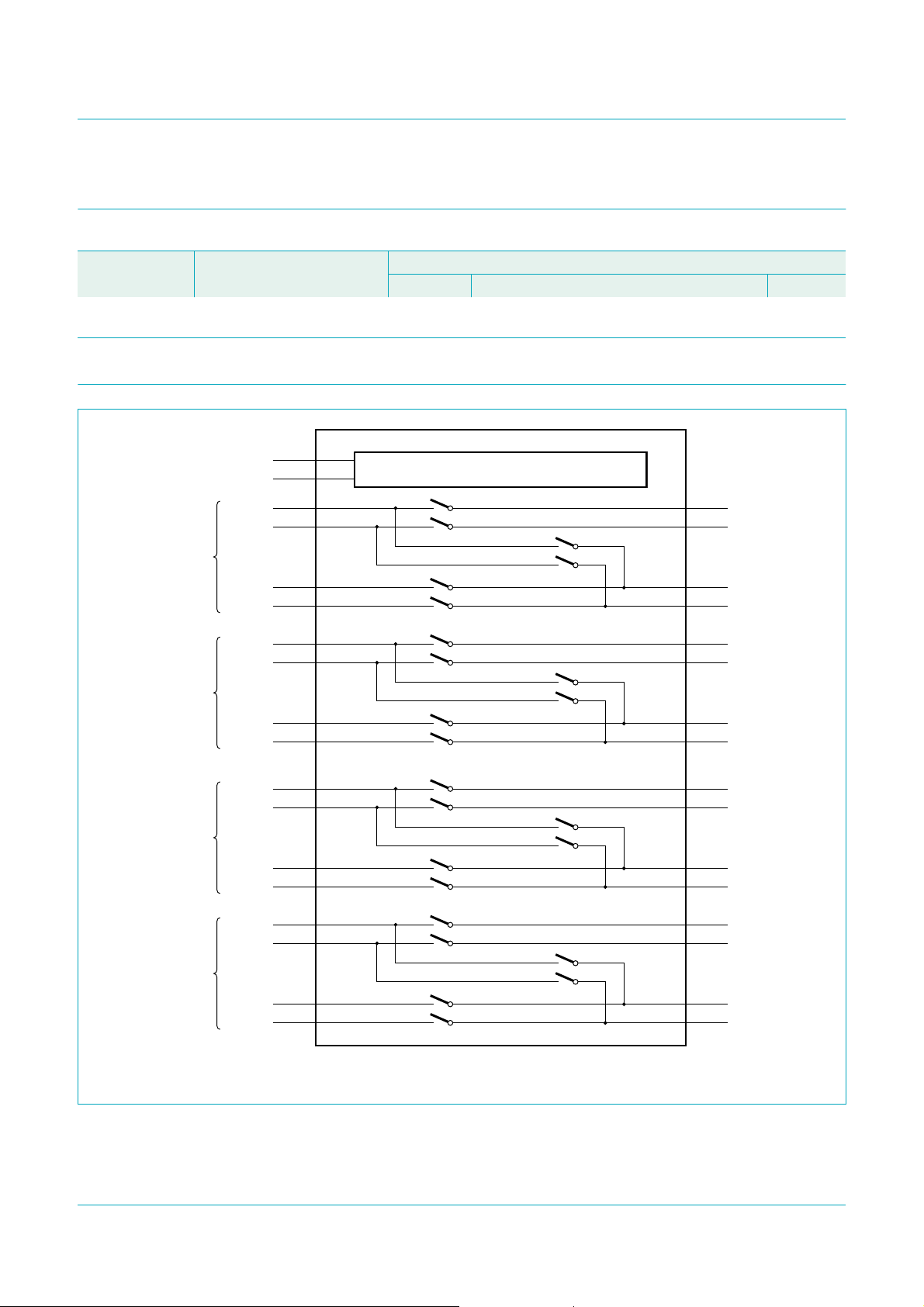
5. Functional diagram
CBTU0808
CTRL[1:0]
TEST[1:0]
CONTROL AND CONFIGURATION
CBTU0808
Dual lane PCI Express port multiplexer
SOT918-1
48 balls; body 5 × 5 × 0.8 mm
channel Tx0
channel Rx0
channel Tx1
TXSA0P
TXSA0N
TXSB0P
TXSB0N
RXSA0P
RXSA0N
RXSB0P
RXSB0N
TXSA1P
TXSA1N
TXSB1P
TXSB1N
RXSA1P
RXSA1N
TXDA0P
TXDA0N
TXDB0P
TXDB0N
LANE 0
RXDA0P
RXDA0N
RXDB0P
RXDB0N
TXDA1P
TXDA1N
TXDB1P
TXDB1N
LANE 1
RXDA1P
RXDA1N
channel Rx1
RXSB1P
RXSB1N
RXDB1P
RXDB1N
002aac139
Fig 1. Functional diagram
CBTU0808_1 © Koninklijke Philips Electronics N.V. 2006. All rights reserved.
Product data sheet Rev. 01 — 2 June 2006 2 of 16
Page 3
Philips Semiconductors
6. Pinning information
6.1 Pinning
CBTU0808
Dual lane PCI Express port multiplexer
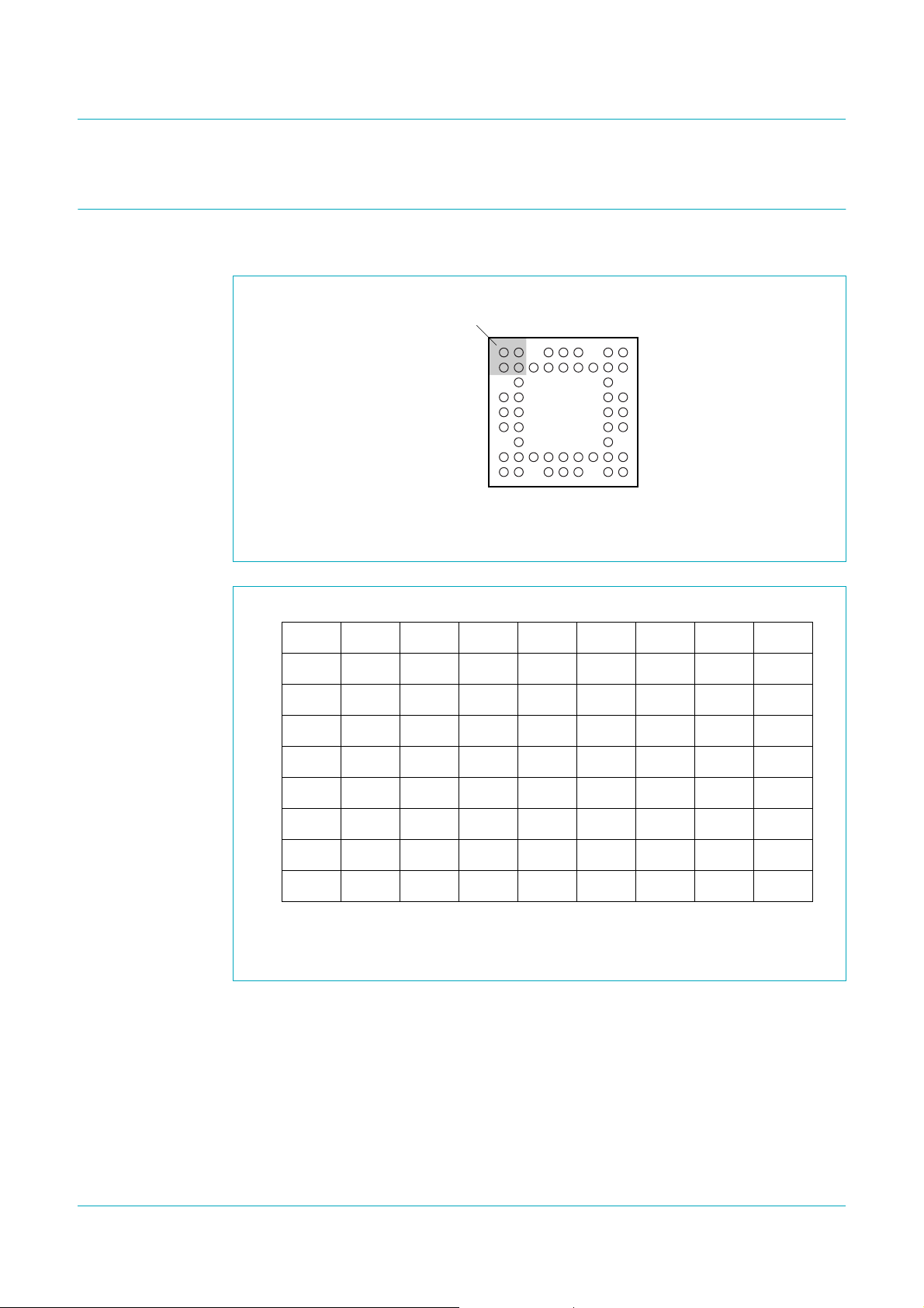
ball A1
index area
A
B
C
D
E
F
G
H
J
Fig 2. Pin configuration for TFBGA48
A
B
C
D
1
CTRL0
RXSA0P
RXSB0P
23456789
TXSB0P TXSA0P GND TXDA0P TXDB0P TEST1
GND TXSB0N TXSA0N V
RXSA0N RXDA0N
RXSB0N RXDB0N RXDB0P
CBTU0808EE/G
246891357
002aac213
Transparent top view
TXDA0N TXDB0N GND RXDA0P
DD
E
F
G
H
J
GND
TXSA1P
TXSB1P
TEST0
V
DD
TXSA1N TXDA1N TXDA1P
TXSB1N TXDB1N
GND RXSA1N RXSB1N V
RXSA1P RXSB1P GND RXDB1P RXDA1P CTRL1
RXDB1N RXDA1N GND TXDB1P
DD
V
DD
GND
002aac212
48-ball, 9 × 9 grid; top view. An empty cell indicates no ball is populated at that grid point.
Fig 3. Ball mapping
CBTU0808_1 © Koninklijke Philips Electronics N.V. 2006. All rights reserved.
Product data sheet Rev. 01 — 2 June 2006 3 of 16
Page 4

Philips Semiconductors
6.2 Pin description
Table 2. Pin description
Signal group Symbol Pin Type Description
Test and
control
Signal ports TXSA0P, TXSA0N,
Power V
CBTU0808
Dual lane PCI Express port multiplexer
CTRL0 A1 CMOS
CTRL1 J9
TEST0 J1 CMOS
TEST1 A9 output Test output. Used for test purposes only.
A4, B4,
TXSB0P, TXSB0N
RXSA0P, RXSA0N,
RXSB0P, RXSB0N
TXSA1P, TXSA1N,
TXSB1P, TXSB1N
RXSA1P, RXSA1N,
RXSB1P, RXSB1N
TXDA0P, TXDA0N,
TXDB0P, TXDB0N
RXDA0P, RXDA0N,
RXDB0P, RXDB0N
TXDA1P, TXDA1N,
TXDB1P, TXDB1N
RXDA1P, RXDA1N,
RXDB1P, RXDB1N
DD
GND A5, B2,
A2, B3
B1, C2,
D1, D2
F1, F2,
H1, G2
J2, H3,
J4, H4
A6, B6,
A8, B7
B9, C8,
D9, D8
F9, F8,
H9, G8
J8, H7,
J6, H6
B5, E2,
E8, H5
B8, E1,
E9, H2,
H8, J5
input
input
signal
port
signal
port
signal
port
signal
port
signal
port
signal
port
signal
port
signal
port
power power supply pins
power ground pins
Switch configuration control inputs. See
Table 3 “Switch configuration truth table”.
Test input. Used for test purposes only.
Should beleftopen-circuit during normal
operation. An internal pull-down resistor
will default this pin to a LOW state.
Should be left open-circuit in normal
application.
Transmit ports A and B differential signal
terminals for Lane 0, Source side.
Receive ports A and B differential signal
terminals for Lane 0, Source side.
Transmit ports A and B differential signal
terminals for Lane 1, Source side.
Receive ports A and B differential signal
terminals for Lane 1, Source side.
Transmit ports A and B differential signal
terminals for Lane 0, Destination side.
Receive ports A and B differential signal
terminals for Lane 0, Destination side.
Transmit ports A and B differential signal
terminals for Lane 1, Destination side.
Receive ports A and B differential signal
terminals for Lane 1, Destination side.
CBTU0808_1 © Koninklijke Philips Electronics N.V. 2006. All rights reserved.
Product data sheet Rev. 01 — 2 June 2006 4 of 16
Page 5

Philips Semiconductors
7. Functional description
7.1 Functional description
7.1.1 General information
The CBTU0808 Dual lane PCI Express port multiplexeris designed to allow port switching
of up to two PCI Express lanes (each including a Transmit and Receive channel)
according to three switch configuration settings (described in Section 7.1.2.1). The basic
switch element of the CBTU0808 is designed integrally with its package and chip
interconnect to present an optimum characteristic on-impedance when used in a
PCI Express signaling environment, and to provide high off-port isolation and low
crosstalk.
7.1.2 Functional information
The following paragraphs describe the control and configuration possibilities available in
the CBTU0808.
7.1.2.1 Switch configuration
The position of the port switches is controlled by CMOS input signals CTRL[1:0] and can
be overridden by CMOS input TEST0 to disconnect (open) all ports between source and
destination. For a given lane, the switch positions are always identical between transmit
and receive channels. Lane 0 is controlled by CTRL0 and Lane 1 is controlled by CTRL1.
The truth table for the switch position as a function of these inputs is shown in Table 3.
CBTU0808
Dual lane PCI Express port multiplexer
Table 3. Switch configuration truth table
Inputs Function
[1]
CTRLn
LOW LOW An R
HIGH
LOW HIGH An high-Z high-Z All ports open-circuit
> LOW HIGH Test mode for internal use only do not use
[1] n is the Lane number (0 or 1).
[2] CTRL1 or CTRL0 = HIGH.
TEST0 Source ports
Bn high-Z R
[2]
LOW An high-Z R
Bn high-Z high-Z
Bn high-Z high-Z
[1]
Destination ports Comment
A B
on
high-Z SA:DA/SB:DB
on
on
(Dual Through mode)
SA:DB
(Single Cross mode)
(Disconnect mode)
CBTU0808_1 © Koninklijke Philips Electronics N.V. 2006. All rights reserved.
Product data sheet Rev. 01 — 2 June 2006 5 of 16
Page 6

Philips Semiconductors
CBTU0808
Dual lane PCI Express port multiplexer
8. Limiting values
Table 4. Limiting values
In accordance with the Absolute Maximum Rating System (IEC 60134).
Symbol Parameter Conditions Min Max Unit
V
DD
V
I
I
IK
I
OK
I
O
I
CCC
T
stg
V
esd
[1] The input and output negative-voltage ratings may be exceeded if the input and output current ratings are observed.
supply voltage −0.5 +2.5 V
input voltage
input clamping current VI< 0 V or VI>V
output clamping current VO< 0 V or VO>V
DD
DD
output current continuous; 0 V < VO< V
continuous current through each
V
or GND pin
DD
DD
[1]
−0.5 +2.5 V
- −50 mA
- ±50 mA
- ±50 mA
- ±100 mA
storage temperature −65 +150 °C
electrostatic discharge voltage Human Body Model; 1.5 kΩ; 100 pF >2 - kV
Machine Model; 0 Ω; 200 pF >200 - V
9. Recommended operating conditions
Table 5. Recommended operating conditions
Symbol Parameter Conditions Min Typ Max Unit
V
DD
V
I
V
IH
V
IL
V
ICR
V
I(dif)(p-p)
T
amb
[1] The CTRL[1:0] inputs of the device must be held at valid levels (not floating) to ensure proper device operation.
[2] V
supply voltage 1.7 - 1.9 V
input voltage TXn and RXn ports −0.25 - +1.75 V
HIGH-level input voltage CTRL[1:0], TEST inputs
LOW-level input voltage CTRL[1:0], TEST[1:0] inputs
common mode input voltage
TXn and RXn ports 0 - 1.5 V
[1]
0.65 × V
[1]
- - 0.35 × V
-V
DD
range
peak-to-peak differential
TXn and RXn ports
[2]
- - 1.2 V
input voltage
ambient temperature operating in free air 0 - +85 °C
I(dif)(p-p)
=2×|V
TX_D+
− V
|. See Paragraph 4.3.3, Table 4-5 of Ref. 1.
TX_D−
DD
DD
V
V
CBTU0808_1 © Koninklijke Philips Electronics N.V. 2006. All rights reserved.
Product data sheet Rev. 01 — 2 June 2006 6 of 16
Page 7

Philips Semiconductors
CBTU0808
Dual lane PCI Express port multiplexer
10. Static characteristics
Table 6. Static characteristics
Over recommended operating conditions, unless otherwise noted.
Symbol Parameter Conditions Min Typ Max Unit
I
DD
supply current
Digital inputs CTRL[1:0] and TEST0
I
LI
C
i
input leakage current VI=VDD or GND - - ±5 µA
input capacitance VI=VDD or GND - - 5 pF
Signal ports TXSA0P … RXDB1N
I
LI
R
on(sw)
∆R
on(sw)
input leakage current VI=VDD or GND; TEST0 = HIGH
switch on-state resistance 8 10 12 Ω
switch on-state resistance
variation
C
S(ON)
ON-state capacitance VI= 0.9 V
(Disconnect mode)
over recommended VID (input
voltage) range
switch; simulated value of the
silicon switch only, excluding
package parasitics
[1]
--1mA
−100 - +100 µA
- 0.5 0.75 Ω
- 3.6 4.75 pF
[1] Static operating current.
CBTU0808_1 © Koninklijke Philips Electronics N.V. 2006. All rights reserved.
Product data sheet Rev. 01 — 2 June 2006 7 of 16
Page 8

Philips Semiconductors
CBTU0808
Dual lane PCI Express port multiplexer
11. Dynamic characteristics
Table 7. Dynamic characteristics
Over recommended operating conditions, unless otherwise noted. Characterization bandwidth: 10 MHz < f
Symbol Parameter Conditions Min Typ Max Unit
t
PD
t
startup
propagation delay Figure 5 -60-ps
start-up time supply voltage valid to switch specified operating
- - 100 µs
characteristics
t
rcfg
reconfiguration time CTRL[1:0], TEST0 setting change to switch specified
- - 100 µs
operating characteristics
t
sk(o)
t
sk(edge)
t
sk(dif)
s
12
output skew time difference in propagation delay between any two ‘ON’
paths within a channel;
Figure 6
edge skew time difference of rising edge propagation delay to falling
edge propagation delay;
Figure 7
differential skew time difference in propagation delay between two
reverse transmission
coefficient
members of a differential pair;
Differential mode ON insertion loss; ON-state
f = 50 MHz −0.8 - - dB
Figure 8
--40ps
--40ps
--5ps
f = 625 MHz −2- - dB
f ≤ 1.25 GHz −3.3 - - dB
s
21
forward transmission
coefficient
Differential mode ON insertion loss; ON-state
f = 50 MHz −0.8 - - dB
f = 625 MHz −2- - dB
f ≤ 1.25 GHz −3.3 - - dB
s
11
input reflection
coefficient
Differential mode ON return loss; ON-state
f = 50 MHz - - −20 dB
f = 625 MHz - - −8dB
f ≤ 1.25 GHz - - −6.0 dB
s
22
output reflection
coefficient
Differential mode ON return loss; ON-state
f = 50 MHz - - −20 dB
f = 625 MHz - - −8dB
f ≤ 1.25 GHz - - −6.0 dB
s
12
reverse transmission
coefficient
Differential mode port-to-port crosstalk;
ON/OFF-state
f=50MHz - - −35 dB
f = 625 MHz - - −35 dB
f = 1.25 GHz - - −35 dB
s
21
forward transmission
coefficient
Differential mode port-to-port crosstalk;
ON/OFF-state
f=50MHz - - −35 dB
f = 625 MHz - - −35 dB
f = 1.25 GHz - - −35 dB
oper
< 6 GHz.
CBTU0808_1 © Koninklijke Philips Electronics N.V. 2006. All rights reserved.
Product data sheet Rev. 01 — 2 June 2006 8 of 16
Page 9
Philips Semiconductors
CBTU0808
Dual lane PCI Express port multiplexer
Table 7. Dynamic characteristics
Over recommended operating conditions, unless otherwise noted. Characterization bandwidth: 10 MHz < f
…continued
oper
< 6 GHz.
Symbol Parameter Conditions Min Typ Max Unit
s
12
reverse transmission
coefficient
Differential mode off-port feedthrough; OFF-state
f=50MHz - - −35 dB
f = 625 MHz - - −35 dB
f = 1.25 GHz - - −35 dB
s
21
forward transmission
coefficient
Differential mode off-port feedthrough; OFF-state
f=50MHz - - −35 dB
f = 625 MHz - - −35 dB
f = 1.25 GHz - - −35 dB
0
s
, s21,
11
, s
s
12
22
(dB)
−6
−12
−18
(1)
(2)
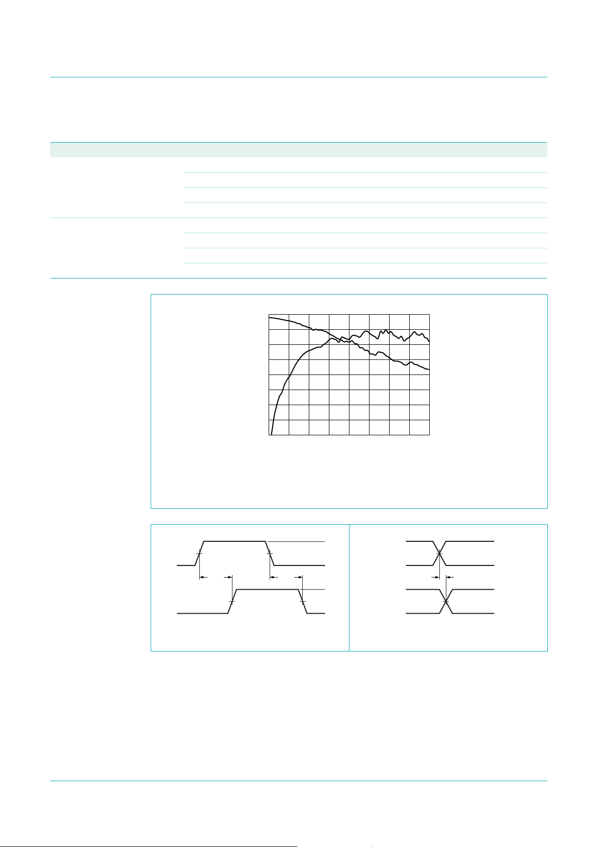
002aac278
−24
0 5.003.751.25 2.50
f (GHz)
(1) insertion loss
(2) return loss
Fig 4. S parameters
1.8 V
output
0.9 V 0.9 Vinput
0 V
t
PLH
V
ref
t
PHL
V
V
ref
V
002aac274
OH
OL
output
output
Fig 5. Propagation delay Fig 6. Output skew
t
sk(o)
V
OH
V
OL
V
OH
V
OL
002aac275
CBTU0808_1 © Koninklijke Philips Electronics N.V. 2006. All rights reserved.
Product data sheet Rev. 01 — 2 June 2006 9 of 16
Page 10
Philips Semiconductors
CBTU0808
Dual lane PCI Express port multiplexer
input
output
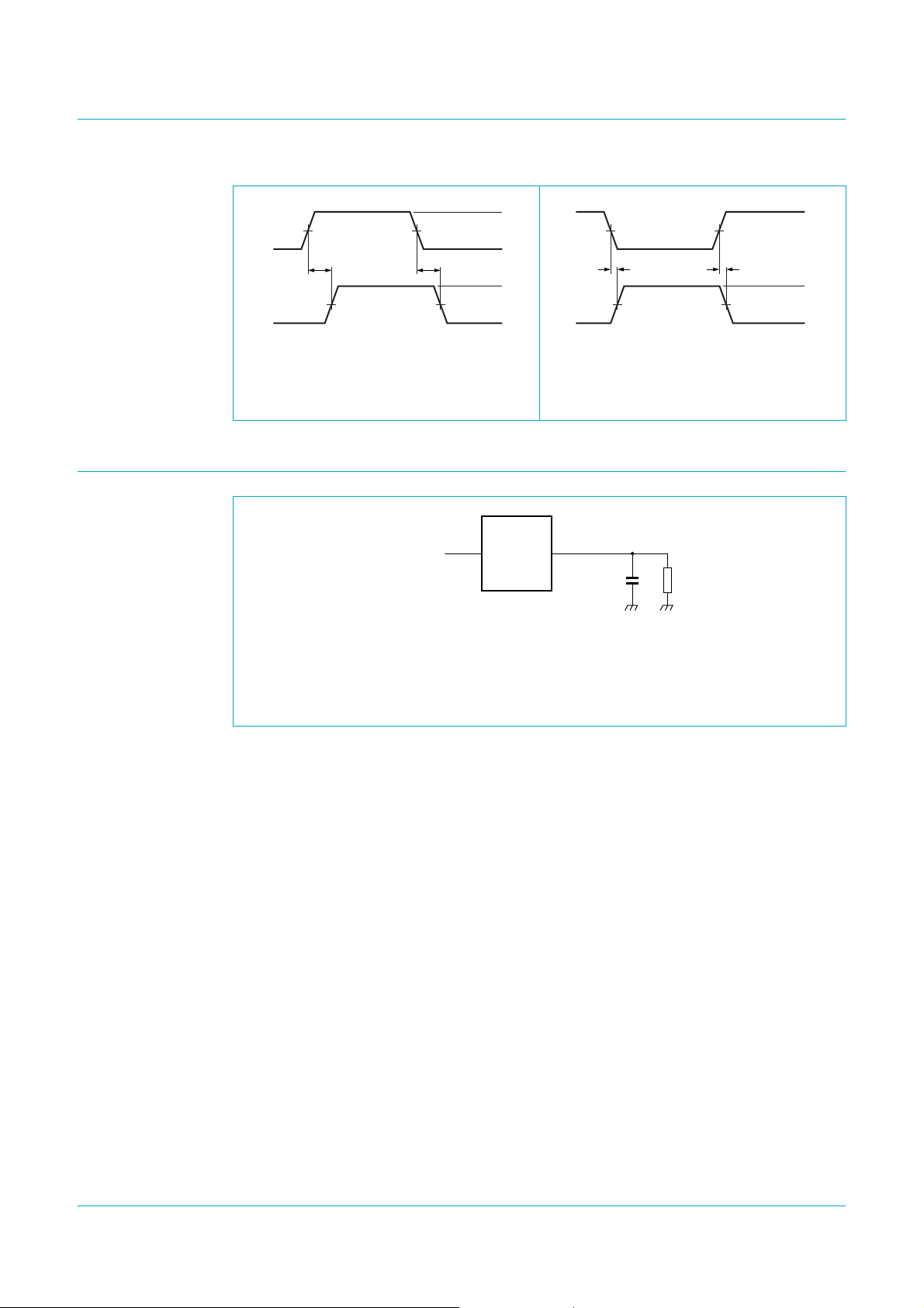
Fig 7. Edge skew Fig 8. Differential skew
12. Test information
Fig 9. Test circuit
1.8 V
OH
OL
input
t
sk(dif)
input
TXDx, RXDx
0.9 V 0.9 V
C
6 pF
L
50 Ω
002aac273
0.9 V 0.9 V
t
PLH
t
=
sk(edge)
|t
rising − t
sk(edge)
sk(edge)
TXSx, RXSx
t
PHL
falling|
0 V
V
0.9 V0.9 V
V
002aac277
DUT
CL represents board and jig and does not indicate additional capacitance.
All input pulses are supplied by generators having the following characteristics:
PRR ≤ 10 MHz; Zo=50Ω; slew rate = 2.5 V/ns
0.9 V0.9 V
t
sk(dif)
1.8 V
0 V
1.8 V
0 V
002aac276
CBTU0808_1 © Koninklijke Philips Electronics N.V. 2006. All rights reserved.
Product data sheet Rev. 01 — 2 June 2006 10 of 16
Page 11
Philips Semiconductors
13. Package outline
CBTU0808
Dual lane PCI Express port multiplexer
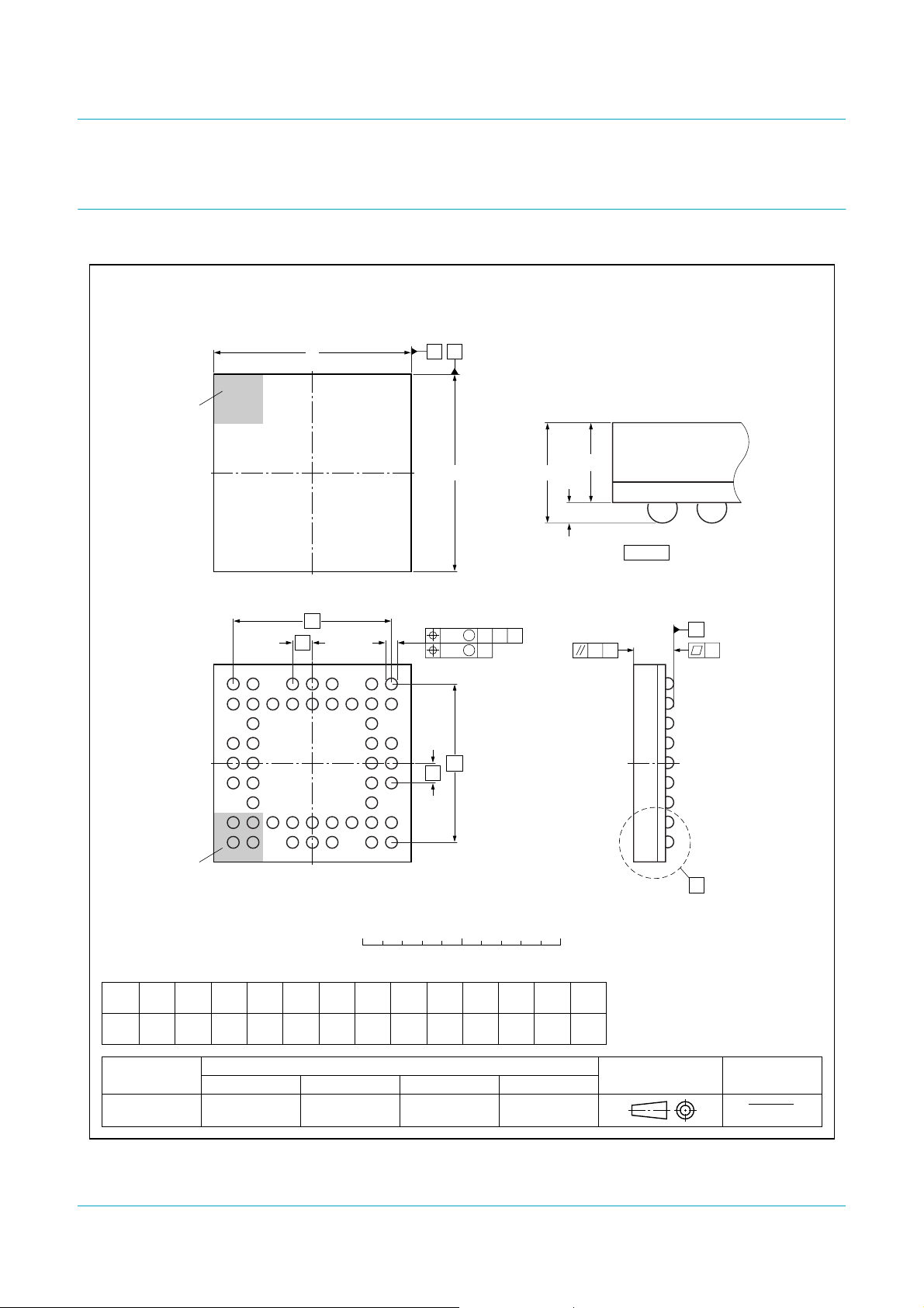
TFBGA48: plastic thin fine-pitch ball grid array package; 48 balls; body 5 x 5 x 0.8 mm
B A
∅ v
e
E
M
AC
M
C∅ w
e
2
A
A
1
B
ball A1
index area
ball A1
index area
D
e
1
e
J
H
G
F
E
D
C
B
A
246813579
b
SOT918-1
A
2
detail X
C
y
C
1
y
X
0 2.5 5 mm
scale
DIMENSIONS (mm are the original dimensions)
A
UNIT
mm 1.15
OUTLINE
VERSION
SOT918-1 MO-195- - - - - -
max
A
0.25
0.15
A
1
b D E e
2
0.90
0.35
5.1
0.75
0.25
IEC JEDEC JEITA
4.9
5.1
4.9
e
e
1
4
0.5
REFERENCES
v
2
0.15w0.05y0.08
4
y
0.1
1
EUROPEAN
PROJECTION
ISSUE DATE
05-09-21
05-10-13
Fig 10. Package outline SOT918-1 (TFBGA48)
CBTU0808_1 © Koninklijke Philips Electronics N.V. 2006. All rights reserved.
Product data sheet Rev. 01 — 2 June 2006 11 of 16
Page 12

Philips Semiconductors
14. Soldering
14.1 Introduction to soldering surface mount packages
There is no soldering method that is ideal for all surface mount IC packages. Wave
soldering can still be used for certain surface mount ICs, but it is not suitable for fine pitch
SMDs. In these situations reflow soldering is recommended.
14.2 Reflow soldering
Reflow soldering requires solder paste (a suspension of fine solder particles, flux and
binding agent) to be applied to the printed-circuit board by screen printing, stencilling or
pressure-syringe dispensing before package placement. Driven by legislation and
environmental forces the worldwide use of lead-free solder pastes is increasing.
Several methods exist for reflowing; for example, convection or convection/infrared
heating in a conveyor type oven. Throughput times (preheating, soldering and cooling)
vary between 100 seconds and 200 seconds depending on heating method.
Typical reflow temperatures range from 215 °Cto260°C depending on solder paste
material. The peak top-surface temperature of the packages should be kept below:
CBTU0808
Dual lane PCI Express port multiplexer
Table 8. SnPb eutectic process - package peak reflow temperatures (from
July 2004)
Package thickness Volume mm3 < 350 Volume mm3≥ 350
< 2.5 mm 240 °C+0/−5 °C 225 °C+0/−5 °C
≥ 2.5 mm 225 °C+0/−5 °C 225 °C+0/−5 °C
Table 9. Pb-free process - package peak reflow temperatures (from
2004)
Package thickness Volume mm3 < 350 Volume mm3 350 to
< 1.6 mm 260 °C + 0 °C 260 °C + 0 °C 260 °C + 0 °C
1.6 mm to 2.5 mm 260 °C + 0 °C 250°C + 0 °C 245 °C + 0 °C
≥ 2.5 mm 250 °C + 0 °C 245 °C + 0 °C 245 °C + 0 °C
Moisture sensitivity precautions, as indicated on packing, must be respected at all times.
14.3 Wave soldering
Conventional single wave soldering is not recommended for surface mount devices
(SMDs) or printed-circuit boards with a high component density, as solder bridging and
non-wetting can present major problems.
To overcome these problems the double-wave soldering method was specifically
developed.
2000
J-STD-020C
J-STD-020C
Volume mm3 > 2000
July
If wave soldering is used the following conditions must be observed for optimal results:
• Use a double-wave soldering method comprising a turbulent wave with high upward
pressure followed by a smooth laminar wave.
• For packages with leads on two sides and a pitch (e):
CBTU0808_1 © Koninklijke Philips Electronics N.V. 2006. All rights reserved.
Product data sheet Rev. 01 — 2 June 2006 12 of 16
Page 13

Philips Semiconductors
– larger than or equal to 1.27 mm, the footprint longitudinal axis is preferred to be
– smaller than 1.27 mm, the footprint longitudinal axis must be parallel to the
The footprint must incorporate solder thieves at the downstream end.
• For packages with leads on four sides, the footprint must be placed at a 45° angle to
the transport direction of the printed-circuit board. The footprint must incorporate
solder thieves downstream and at the side corners.
During placement and before soldering, the package must be fixed with a droplet of
adhesive. The adhesive can be applied by screen printing, pin transfer or syringe
dispensing. The package can be soldered after the adhesive is cured.
Typical dwell time of the leads in the wave ranges from 3 seconds to 4 seconds at 250 °C
or 265 °C, depending on solder material applied, SnPb or Pb-free respectively.
A mildly-activated flux will eliminate the need for removal of corrosive residues in most
applications.
CBTU0808
Dual lane PCI Express port multiplexer
parallel to the transport direction of the printed-circuit board;
transport direction of the printed-circuit board.
14.4 Manual soldering
Fix the component by first soldering two diagonally-opposite end leads. Use a low voltage
(24 V or less) soldering iron applied to the flat part of the lead. Contact time must be
limited to 10 seconds at up to 300 °C.
When using a dedicated tool, all other leads can be soldered in one operation within
2 seconds to 5 seconds between 270 °C and 320 °C.
14.5 Package related soldering information
Table 10. Suitability of surface mount IC packages for wave and reflow soldering methods
Package
BGA, HTSSON..T
SSOP..T
DHVQFN, HBCC, HBGA, HLQFP, HSO, HSOP,
HSQFP, HSSON, HTQFP, HTSSOP, HVQFN,
HVSON, SMS
PLCC
LQFP, QFP, TQFP not recommended
SSOP, TSSOP, VSO, VSSOP not recommended
CWQCCN..L
[1]
[3]
[3]
, TFBGA, VFBGA, XSON
[5]
, SO, SOJ suitable suitable
, LBGA, LFBGA, SQFP,
[8]
, PMFP
[9]
, WQCCN..L
[8]
Soldering method
Wave Reflow
not suitable suitable
not suitable
not suitable not suitable
[2]
[4]
[5][6]
[7]
suitable
suitable
suitable
[1] For more detailed information on the BGA packages refer to the
order a copy from your Philips Semiconductors sales office.
[2] All surface mount (SMD) packages are moisture sensitive. Depending upon the moisture content, the
maximum temperature (with respect to time) and body size of the package, there is a risk that internal or
external package cracks may occur due to vaporization of the moisture in them (the so called popcorn
effect). For details, refer to the Drypack information in the
Packages; Section: Packing Methods
CBTU0808_1 © Koninklijke Philips Electronics N.V. 2006. All rights reserved.
Product data sheet Rev. 01 — 2 June 2006 13 of 16
.
(LF)BGA Application Note
Data Handbook IC26; Integrated Circuit
(AN01026);
Page 14

Philips Semiconductors
[3] These transparent plastic packages are extremely sensitive to reflow soldering conditions and must on no
account be processed through more than one soldering cycle or subjected to infrared reflow soldering with
peak temperature exceeding 217 °C ± 10 °C measured in the atmosphere of the reflow oven. The package
body peak temperature must be kept as low as possible.
[4] These packages are not suitable for wave soldering. On versions with the heatsink on the bottom side, the
solder cannot penetrate between the printed-circuit board and the heatsink. On versions with the heatsink
on the top side, the solder might be deposited on the heatsink surface.
[5] If wave soldering is considered, then the package must be placed at a 45° angle to the solder wave
direction. The package footprint must incorporate solder thieves downstream and at the side corners.
[6] Wave soldering is suitable for LQFP, QFP and TQFP packages with a pitch (e) larger than 0.8 mm; it is
definitely not suitable for packages with a pitch (e) equal to or smaller than 0.65mm.
[7] Wavesoldering is suitable for SSOP, TSSOP, VSO and VSSOP packages with a pitch (e) equal to or larger
than 0.65 mm; it is definitely not suitable for packages with a pitch (e) equal to or smaller than 0.5 mm.
[8] Image sensor packages in principle should not be soldered. They are mounted in sockets or delivered
pre-mounted on flex foil. However, the image sensor package can be mounted by the client on a flex foil by
using a hot bar soldering process. The appropriate soldering profile can be provided on request.
[9] Hot bar soldering or manual soldering is suitable for PMFP packages.
15. Abbreviations
CBTU0808
Dual lane PCI Express port multiplexer
Table 11. Abbreviations
Acronym Description
CMOS Complementary Metal Oxide Semiconductor
PCI Peripheral Component Interconnect
PCIe PCI Express
DUT Device Under Test
ESD ElectroStatic Discharge
HBM Human Body Model
PRR Pulse Repetition Rate
MM Machine Model
16. References
[1] PCI Express Base Specification, Rev 1.1 — Revision 1.1, March 2005.
17. Revision history
Table 12. Revision history
Document ID Release date Data sheet status Change notice Supersedes
CBTU0808_1 20060602 Product data sheet - -
CBTU0808_1 © Koninklijke Philips Electronics N.V. 2006. All rights reserved.
Product data sheet Rev. 01 — 2 June 2006 14 of 16
Page 15

Philips Semiconductors
18. Legal information
18.1 Data sheet status
CBTU0808
Dual lane PCI Express port multiplexer
Document status
Objective [short] data sheet Development This document contains data from the objective specification for product development.
Preliminary [short] data sheet Qualification This document contains data from the preliminary specification.
Product [short] data sheet Production This document contains the product specification.
[1] Please consult the most recently issued document before initiating or completing a design.
[2] The term ‘short data sheet’ is explained in section “Definitions”.
[3] The product status of device(s) described in this document may have changed since this document was published and may differ in case of multiple devices. The latest product status
information is available on the Internet at URL
[1][2]
Product status
18.2 Definitions
Draft — The document is a draft version only. The content is still under
internal review and subject to formal approval, which may result in
modifications or additions. Philips Semiconductors does not give any
representations or warranties as to the accuracy or completeness of
information included herein and shall have no liability for the consequences of
use of such information.
Short data sheet — A short data sheet is an extract from a full data sheet
with the same product type number(s) and title. A short data sheet is intended
for quick reference only and should not be relied upon to contain detailed and
full information. For detailed and full information see the relevant full data
sheet, which is available on request via the local Philips Semiconductors
sales office. In case of any inconsistency or conflict with the short data sheet,
the full data sheet shall prevail.
18.3 Disclaimers
General — Information in this document is believed to be accurate and
reliable. However, Philips Semiconductors does not give any representations
or warranties, expressed or implied, as to the accuracy or completeness of
such information and shall have no liability for the consequences of use of
such information.
Right to make changes — Philips Semiconductors reserves the right to
make changes to information published in this document, including without
limitation specifications and product descriptions, at any time and without
notice. This document supersedes and replaces all information supplied prior
to the publication hereof.
Suitability for use — Philips Semiconductors products are not designed,
authorized or warranted to be suitable for use in medical, military, aircraft,
space or life support equipment, nor in applications where failure or
[3]
http://www.semiconductors.philips.com.
Definition
malfunction of a Philips Semiconductors product can reasonably be expected
to result in personal injury, death or severe property or environmental
damage. Philips Semiconductors accepts no liability for inclusion and/or use
of Philips Semiconductors products in such equipment or applications and
therefore such inclusion and/or use is for the customer’s own risk.
Applications — Applications that are described herein for any of these
products are for illustrative purposes only. Philips Semiconductors makes no
representation or warranty that such applications will be suitable for the
specified use without further testing or modification.
Limiting values — Stress above one or more limiting values (as defined in
the Absolute Maximum Ratings System of IEC 60134) may cause permanent
damage to the device. Limiting values are stress ratings only and and
operation of the device at these or any other conditions above those given in
the Characteristics sections of this document is not implied. Exposure to
limiting values for extended periods may affect device reliability.
Terms and conditions of sale — Philips Semiconductors products are sold
subject to the general terms and conditions of commercial sale, as published
at
http://www.semiconductors.philips.com/profile/terms, including those
pertaining to warranty, intellectual property rights infringement and limitation
of liability, unless explicitly otherwise agreed to in writing by Philips
Semiconductors. In case of any inconsistency or conflict between information
in this document and such terms and conditions, the latter will prevail.
No offer to sell or license — Nothing in this document may be interpreted
or construed as an offer to sell products that is open for acceptance or the
grant, conveyanceor implication of any license under any copyrights, patents
or other industrial or intellectual property rights.
18.4 Trademarks
Notice: All referencedbrands,product names, service names and trademarks
are the property of their respective owners.
19. Contact information
For additional information, please visit: http://www.semiconductors.philips.com
For sales office addresses, send an email to: [email protected]
CBTU0808_1 © Koninklijke Philips Electronics N.V. 2006. All rights reserved.
Product data sheet Rev. 01 — 2 June 2006 15 of 16
Page 16

Philips Semiconductors
20. Contents
1 General description . . . . . . . . . . . . . . . . . . . . . . 1
2 Features . . . . . . . . . . . . . . . . . . . . . . . . . . . . . . . 1
3 Applications . . . . . . . . . . . . . . . . . . . . . . . . . . . . 1
4 Ordering information. . . . . . . . . . . . . . . . . . . . . 2
5 Functional diagram . . . . . . . . . . . . . . . . . . . . . . 2
6 Pinning information. . . . . . . . . . . . . . . . . . . . . . 3
6.1 Pinning . . . . . . . . . . . . . . . . . . . . . . . . . . . . . . . 3
6.2 Pin description . . . . . . . . . . . . . . . . . . . . . . . . . 4
7 Functional description . . . . . . . . . . . . . . . . . . . 5
7.1 Functional description. . . . . . . . . . . . . . . . . . . . 5
7.1.1 General information . . . . . . . . . . . . . . . . . . . . . 5
7.1.2 Functional information . . . . . . . . . . . . . . . . . . . 5
7.1.2.1 Switch configuration . . . . . . . . . . . . . . . . . . . . . 5
8 Limiting values. . . . . . . . . . . . . . . . . . . . . . . . . . 6
9 Recommended operating conditions. . . . . . . . 6
10 Static characteristics. . . . . . . . . . . . . . . . . . . . . 7
11 Dynamic characteristics . . . . . . . . . . . . . . . . . . 8
12 Test information. . . . . . . . . . . . . . . . . . . . . . . . 10
13 Package outline . . . . . . . . . . . . . . . . . . . . . . . . 11
14 Soldering . . . . . . . . . . . . . . . . . . . . . . . . . . . . . 12
14.1 Introduction to soldering surface mount
packages . . . . . . . . . . . . . . . . . . . . . . . . . . . . 12
14.2 Reflow soldering. . . . . . . . . . . . . . . . . . . . . . . 12
14.3 Wave soldering. . . . . . . . . . . . . . . . . . . . . . . . 12
14.4 Manual soldering . . . . . . . . . . . . . . . . . . . . . . 13
14.5 Package related soldering information . . . . . . 13
15 Abbreviations. . . . . . . . . . . . . . . . . . . . . . . . . . 14
16 References . . . . . . . . . . . . . . . . . . . . . . . . . . . . 14
17 Revision history. . . . . . . . . . . . . . . . . . . . . . . . 14
18 Legal information. . . . . . . . . . . . . . . . . . . . . . . 15
18.1 Data sheet status . . . . . . . . . . . . . . . . . . . . . . 15
18.2 Definitions. . . . . . . . . . . . . . . . . . . . . . . . . . . . 15
18.3 Disclaimers. . . . . . . . . . . . . . . . . . . . . . . . . . . 15
18.4 Trademarks. . . . . . . . . . . . . . . . . . . . . . . . . . . 15
19 Contact information. . . . . . . . . . . . . . . . . . . . . 15
20 Contents . . . . . . . . . . . . . . . . . . . . . . . . . . . . . . 16
CBTU0808
Dual lane PCI Express port multiplexer
Please be aware that important notices concerning this document and the product(s)
described herein, have been included in section ‘Legal information’.
© Koninklijke Philips Electronics N.V. 2006. All rights reserved.
For more information, please visit: http://www.semiconductors.philips.com.
For sales office addresses, email to: [email protected].
Date of release: 2 June 2006
Document identifier: CBTU0808_1
 Loading...