

Page 1
CC1100
Data Sheet (Rev.1.1) SWRS038A Page 1 of 89
CC1100
Single Chip Low Cost Low Power RF Transceiver
Applications
• Ultra low power UHF wireless transceivers
• 315/433/868 and 915 MHz ISM/SRD band
systems
• AMR – Automatic Meter Reading
• Consumer Electronics
• Two-way RKE –Remote Keyless Entry
• Low power telemetry
• Home and building automation
• Wireless alarm and security systems
• Industrial monitoring and control
• Wireless sensor networks
Product Description
The
CC1100
is a low cost true single chip UHF
transceiver designed for very low power
wireless applications. The circuit is mainly
intended for the ISM (Industrial, Scientific and
Medical) and SRD (Short Range Device)
frequency bands at 315, 433, 868 and 915
MHz, but can easily be programmed for
operation at other frequencies in the 300-348
MHz, 400-464 MHz and 800-928 MHz bands.
The RF transceiver is integrated with a highly
configurable baseband modem. The modem
supports various modulation formats and has
a configurable data rate up to 500 kbps. The
communication range can be increased by
enabling a Forward Error Correction option,
which is integrated in the modem.
CC1100
provides extensive hardware support
for packet handling, data buffering, burst
transmissions, clear channel assessment, link
quality indication and wake-on-radio.
The main operating parameters and the 64byte transmit/receive FIFOs of
CC1100
can be
controlled via an SPI interface. In a typical
system, the
CC1100
will be used together with a
microcontroller and a few additional passive
components.
CC1100
is part of Chipcon’s 4th generation
technology platform based on 0.18 µm CMOS
technology.
Key Features
• Small size (QLP 4x4 mm package, 20
pins)
• True single chip UHF RF transceiver
• Frequency bands: 300-348 MHz, 400-464
MHz and 800-928 MHz
• High sensitivity (–110 dBm at 1.2 kbps,
1% packet error rate)
• Programmable data rate up to 500 kbps
• Low current consumption (15.4 mA in RX,
1.2 kbps, 433 MHz)
• Programmable output power up to +10
dBm for all supported frequencies
• Excellent receiver selectivity and blocking
performance
• Very few external components: Totally on-
chip frequency synthesizer, no external
filters or RF switch needed
• Programmable baseband modem
• Ideal for multi-channel operation
• Configurable packet handling hardware
• Suitable for frequency hopping systems
due to a fast settling frequency synthesizer
• Optional Forward Error Correction with
interleaving
• Separate 64-byte RX and TX data FIFOs
• Efficient SPI interface: All registers can be
programmed with one “burst” transfer
Page 2

CC1100
Data Sheet (Rev.1.1) SWRS038A Page 2 of 89
Features (continued from front page)
• Digital RSSI output
• Suited for systems compliant with EN 300
220 (Europe) and FCC CFR Part 15 (US)
• Wake-on-radio functionality for automatic
low-power RX polling
• Many powerful digital features allow a
high-performance RF system to be made
using an inexpensive microcontroller
• Integrated analog temperature sensor
• Lead-free “green“ package
• Flexible support for packet oriented
systems: On chip support for sync word
detection, address check, flexible packet
length and automatic CRC handling
• Programmable channel filter bandwidth
• OOK and flexible ASK shaping supported
• FSK, GFSK and MSK supported.
• Automatic Frequency Compensation
(AFC) can be used to align the frequency
synthesizer to the received centre
frequency
• Optional automatic whitening and de-
whitening of data
• Support for asynchronous transparent
receive/transmit mode for backwards
compatibility with existing radio
communication protocols
• Programmable Carrier Sense (CS)
indicator
• Programmable Preamble Quality Indicator
(PQI) for detecting preambles and
improved protection against sync word
detection in random noise
• Support for automatic Clear Channel
Assessment (CCA) before transmitting (for
listen-before-talk systems)
• Support for per-package Link Quality
Indication
Page 3

CC1100
Data Sheet (Rev.1.1) SWRS038A Page 3 of 89
Abbreviations
Abbreviations used in this data sheet are described below.
ADC Analog to Digital Converter NRZ Non Return to Zero (Coding)
AFC Automatic Frequency Compensation OOK On-Off Keying
AGC Automatic Gain Control PA Power Amplifier
AMR Automatic Meter Reading PCB Printed Circuit Board
ASK Amplitude Shift Keying PD Power Down
BER Bit Error Rate PER Packet Error Rate
CCA Clear Channel Assessment PLL Phase Locked Loop
CFR Code of Federal Regulations POR Power-On Reset
CRC Cyclic Redundancy Check PQI Preamble Quality Indicator
CW Contionus Wave (Unmodulated Carrier) PQT Preamble Quality Threshold
CS Carrier Sense PTAT Proportional To Absolute Temperature
DC Direct Current QLP Quad Leadless Package
DVGA Digital Variable Gain Amplifier QPSK Quadrature Phase Shift Keying
EIRP Equivalent Isotropic Radiated Power RC Resistor-Capacitor
ESR Equivalent Series Resistance RCOSC RC Oscillator
FCC Federal Communications Commission RF Radio Frequency
FEC Forward Error Correction RSSI Received Signal Strength Indicator
FIFO First-In-First-Out RX Receive, Receive Mode
FSK Frequency Shift Keying SAW Surface Aqustic Wave
GFSK Gaussian shaped Frequency Shift Keying SMD Surface Mount Device
IF Intermediate Frequency SNR Signal to Noise Ratio
ISM Industrial, Scientific, Medical SPI Serial Peripheral Interface
LBT Listen Before Transmit SRD Short Range Devices
LC Inductor-Capacitor TBD To Be Defined
LNA Low Noise Amplifier T/R Transmit/Receive
LO Local Oscillator TX Transmit, Transmit Mode
LSB Least Significant Byte UHF Ultra High frequency
LQI Link Quality Indicator VCO Voltage Controlled Oscillator
MCU Microcontroller Unit WOR Wake on Radio, Low power polling
MSK Minimum Shift Keying XOSC Crystal Oscillator
N/A Not Applicable XTAL Crystal
Page 4

CC1100
Data Sheet (Rev.1.1) SWRS038A Page 4 of 89
Table Of Contents
APPLICATIONS...........................................................................................................................................1
PRODUCT DESCRIPTION.........................................................................................................................1
KEY FEATURES..........................................................................................................................................1
FEATURES (CONTINUED FROM FRONT PAGE)................................................................................2
ABBREVIATIONS........................................................................................................................................3
TABLE OF CONTENTS..............................................................................................................................4
1
ABSOLUTE MAXIMUM RATINGS..............................................................................................7
2
OPERATING CONDITIONS ..........................................................................................................7
3
GENERAL CHARACTERISTICS..................................................................................................7
4
ELECTRICAL SPECIFICATIONS................................................................................................8
4.1 C
URRENT CONSUMPTION
.....................................................................................................................8
4.2 RF R
ECEIVE SECTION
.........................................................................................................................10
4.3 RF T
RANSMIT SECTION
......................................................................................................................13
4.4 C
RYSTAL OSCILLATOR
.......................................................................................................................14
4.5 L
OW POWER RC OSCILLATOR
............................................................................................................14
4.6 F
REQUENCY SYNTHESIZER CHARACTERISTICS
...................................................................................15
4.7 A
NALOG TEMPERATURE SENSOR
........................................................................................................16
4.8 DC C
HARACTERISTICS
.......................................................................................................................16
4.9 P
OWER ON RESET
...............................................................................................................................16
5
PIN CONFIGURATION.................................................................................................................17
6
CIRCUIT DESCRIPTION.............................................................................................................19
7
APPLICATION CIRCUIT.............................................................................................................19
8
CONFIGURATION OVERVIEW.................................................................................................23
9
CONFIGURATION SOFTWARE.................................................................................................24
10 4-WIRE SERIAL CONFIGURATION AND DATA INTERFACE...........................................24
10.1 C
HIP STATUS BYTE
............................................................................................................................26
10.2 R
EGISTER ACCESS
..............................................................................................................................26
10.3 SPI R
EAD
...........................................................................................................................................27
10.4 C
OMMAND STROBES
..........................................................................................................................27
10.5 FIFO A
CCESS
.....................................................................................................................................27
10.6 PATABLE A
CCESS
............................................................................................................................28
11 MICROCONTROLLER INTERFACE AND PIN CONFIGURATION...................................28
11.1 C
ONFIGURATION INTERFACE
..............................................................................................................28
11.2 G
ENERAL CONTROL AND STATUS PINS
..............................................................................................28
11.3 O
PTIONAL RADIO CONTROL FEATURE
.................................................................................................29
12 DATA RATE PROGRAMMING...................................................................................................29
13 RECEIVER CHANNEL FILTER BANDWIDTH.......................................................................29
14 DEMODULATOR, SYMBOL SYNCHRONIZER AND DATA DECISION............................30
14.1 F
REQUENCY OFFSET COMPENSATION
.................................................................................................30
14.2 B
IT SYNCHRONIZATION
......................................................................................................................30
14.3 B
YTE SYNCHRONIZATION
...................................................................................................................30
15 PACKET HANDLING HARDWARE SUPPORT.......................................................................31
15.1 D
ATA WHITENING
...............................................................................................................................31
15.2 P
ACKET FORMAT
................................................................................................................................32
15.3 P
ACKET FILTERING IN RECEIVE MODE
...............................................................................................34
15.4 P
ACKET HANDLING IN TRANSMIT MODE
............................................................................................34
15.5 P
ACKET HANDLING IN RECEIVE MODE
..............................................................................................34
16 MODULATION FORMATS..........................................................................................................35
16.1 F
REQUENCY SHIFT KEYING
................................................................................................................35
16.2 M
INIMUM SHIFT KEYING
....................................................................................................................35
Page 5

CC1100
Data Sheet (Rev.1.1) SWRS038A Page 5 of 89
16.3
A
MPLITUDE MODULATION
.................................................................................................................35
17 RECEIVED SIGNAL QUALIFIERS AND LINK QUALITY INFORMATION.....................36
17.1 S
YNC WORD QUALIFIER
.....................................................................................................................36
17.2 P
REAMBLE QUALITY THRESHOLD
(PQT)...........................................................................................36
17.3 RSSI...................................................................................................................................................36
17.4 C
ARRIER SENSE
(CS)..........................................................................................................................38
17.5 C
LEAR CHANNEL ASSESSMENT
(CCA) ..............................................................................................39
17.6 L
INK QUALITY INDICATOR
(LQI).......................................................................................................39
18 FORWARD ERROR CORRECTION WITH INTERLEAVING..............................................39
18.1 F
ORWARD ERROR CORRECTION
(FEC)...............................................................................................39
18.2 I
NTERLEAVING
...................................................................................................................................39
19 RADIO CONTROL.........................................................................................................................41
19.1 P
OWER ON START-UP SEQUENCE
.........................................................................................................41
19.2 C
RYSTAL CONTROL
............................................................................................................................42
19.3 V
OLTAGE REGULATOR CONTROL
.......................................................................................................42
19.4 A
CTIVE MODES
..................................................................................................................................43
19.5 W
AKE ON RADIO
(WOR) ...................................................................................................................43
19.6 T
IMING
...............................................................................................................................................44
19.7 RX T
ERMINATION TIMER
...................................................................................................................44
20 DATA FIFO.....................................................................................................................................45
21 FREQUENCY PROGRAMMING.................................................................................................46
22 VCO..................................................................................................................................................47
22.1 VCO
AND
PLL S
ELF-CALIBRATION
...................................................................................................47
23 VOLTAGE REGULATORS ..........................................................................................................47
24 OUTPUT POWER PROGRAMMING.........................................................................................48
25 SELECTIVITY................................................................................................................................49
26 CRYSTAL OSCILLATOR.............................................................................................................51
26.1 R
EFERENCE SIGNAL
............................................................................................................................51
27 EXTERNAL RF MATCH ..............................................................................................................51
28 GENERAL PURPOSE / TEST OUTPUT CONTROL PINS......................................................52
29 ASYNCHRONOUS AND SYNCHRONOUS SERIAL OPERATION.......................................54
29.1 A
SYNCHRONOUS OPERATION
..............................................................................................................54
29.2 S
YNCHRONOUS SERIAL OPERATION
....................................................................................................54
30 SYSTEM CONSIDERATIONS AND GUIDELINES..................................................................54
30.1 SRD R
EGULATIONS
............................................................................................................................54
30.2 F
REQUENCY HOPPING AND MULTI-CHANNEL SYSTEMS
.....................................................................55
30.3 W
IDEBAND MODULATION NOT USING SPREAD SPECTRUM
.................................................................55
30.4 D
ATA BURST TRANSMISSIONS
............................................................................................................55
30.5 C
ONTINUOUS TRANSMISSIONS
...........................................................................................................55
30.6 C
RYSTAL DRIFT COMPENSATION
.......................................................................................................55
30.7 S
PECTRUM EFFICIENT MODULATION
..................................................................................................56
30.8 L
OW COST SYSTEMS
..........................................................................................................................56
30.9 B
ATTERY OPERATED SYSTEMS
..........................................................................................................56
30.10 I
NCREASING OUTPUT POWER
.........................................................................................................56
31 CONFIGURATION REGISTERS.................................................................................................56
31.1 C
ONFIGURATION REGISTER DETAILS – REGISTERS WITH PRESERVED VALUES IN SLEEP STATE
..........61
31.2 C
ONFIGURATION REGISTER DETAILS – REGISTERS THAT LOOSE PROGRAMMING IN SLEEP STATE
......80
31.3 S
TATUS REGISTER DETAILS
.................................................................................................................81
32 PACKAGE DESCRIPTION (QLP 20)..........................................................................................84
32.1 R
ECOMMENDED
PCB
LAYOUT FOR PACKAGE
(QLP 20).....................................................................85
32.2 P
ACKAGE THERMAL PROPERTIES
........................................................................................................85
32.3 S
OLDERING INFORMATION
..................................................................................................................85
32.4 T
RAY SPECIFICATION
..........................................................................................................................86
32.5 C
ARRIER TAPE AND REEL SPECIFICATION
...........................................................................................86
Page 6

CC1100
Data Sheet (Rev.1.1) SWRS038A Page 6 of 89
33
ORDERING INFORMATION.......................................................................................................86
34 GENERAL INFORMATION.........................................................................................................87
34.1 D
OCUMENT HISTORY
.........................................................................................................................87
34.2 P
RODUCT STATUS DEFINITIONS
.........................................................................................................87
35 ADDRESS INFORMATION..........................................................................................................88
36 TI WORLDWIDE TECHNICAL SUPPORT...............................................................................88
Page 7
CC1100
Data Sheet (Rev.1.1) SWRS038A Page 7 of 89
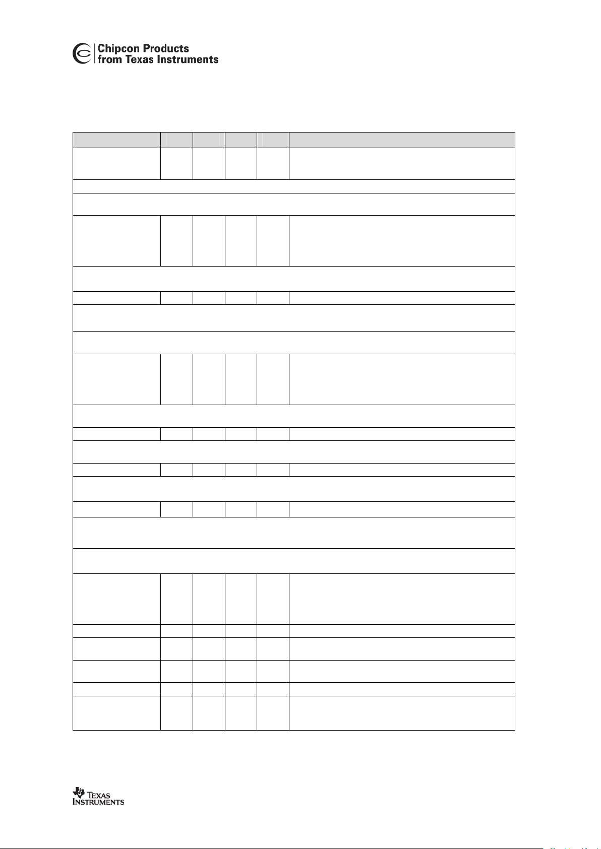
1 Absolute Maximum Ratings
Under no circumstances must the absolute maximum ratings given in Table 1 be violated. Stress
exceeding one or more of the limiting values may cause permanent damage to the device.
Caution! ESD sensitive device.
Precaution should be used when handling
the device in order to prevent permanent
damage.
Parameter Min Max Units Condition
Supply voltage –0.3 3.6 V All supply pins must have the same voltage
Voltage on any digital pin –0.3 VDD+0.3
max 3.6
V
Voltage on the pins RF_P, RF_N
and DCOUPL
–0.3 2.0 V
Voltage ramp-up 120 kV/µs
Input RF level +10 dBm
Storage temperature range –50 150
°C
Solder reflow temperature 260
°C
According to IPC/JEDEC J-STD-020C
ESD <500 V According to JEDEC STD 22, method A114,
Human Body Model
Table 1: Absolute Maximum Rati ngs
2 Operating Conditions
The operating conditions for
CC1100
are listed Table 2 in below.
Parameter Min Max Unit Condition
Operating temperature -40 85
°C
Operating supply voltage 1.8 3.6 V All supply pins must have the same voltage
Table 2: Operating Condi tions
3 General Characteristics
Parameter Min Typ Max Unit Condition/Note
Frequency range 300 348 MHz
400 464 MHz
800 928 MHz
Data rate 1.2
1.2
26
500
250
500
kbps
kbps
kbps
FSK
GFSK, OOK and ASK
(Shaped) MSK (also known as differential offset
QPSK)
Optional Manchester encoding (halves the data rate).
Table 3: General Characteristics
Page 8
CC1100
Data Sheet (Rev.1.1) SWRS038A Page 8 of 89
4 Electrical Specifications
4.1 Current Consumption
Tc = 25°C, VDD = 3.0V if nothing else stated. All measurement results are obtained using the CC1100EM reference
design.
Reduced current settings (MDMCFG2.DEM_DCFILT_OFF = 1) gives a slightly lower current consumption at the cost of a
reduction in sensitivity. See Table 5 for additional details on current consumption and sensitivity.
Parameter Min Typ Max Unit Condition
400 nA Voltage regulator to digital part off, register values retained
(SLEEP state)
900 nA Voltage regulator to digital part off, register values retained, low-
power RC oscillator running (SLEEP state with WOR enabled)
95
µA
Voltage regulator to digital part off, register values retained,
XOSC running (SLEEP state with MCSM0.OSC_FORCE_ON set)
Current consumption in power
down modes
160
µA
Voltage regulator to digital part on, all other modules in power
down (XOFF state)
8.7
µA
Automatic RX polling once each second, using low-power RC
oscillator, with 460 kHz filter bandwidth and 250 kbps data rate,
PLL calibration every 4
th
wakeup. Average current with signal in
channel below carrier sense level.
40
µA
Same as above, but with signal in channel above carrier sense
level, 1.9ms RX timeout, and no preamble/sync word found.
1.5
µA
Automatic RX polling every 15th second, using low-power RC
oscillator, with 460kHz filter bandwidth and 250kbps data rate,
PLL calibration every 4
th
wakeup. Average current with signal in
channel below carrier sense level.
46
µA
Same as above, but with signal in channel above carrier sense
level, 37ms RX timeout, and no preamble/sync word found.
1.6 mA Only voltage regulator to digital part and crystal oscillator running
(IDLE state)
Current consumption
8.2 mA Only the frequency synthesizer running (after going from IDLE
until reaching RX or TX states, and frequency calibration states)
Current consumption,
315MHz
27.0
14.8
12.3
15.1
13.9
14.9
14.1
16.0
14.5
mA Transmit mode, +10dBm output power
Transmit mode, 0dBm output power
Transmit mode, –6dBm output power
Receive mode, 1.2kbps, reduced current, input at sensitivity limit
Receive mode, 1.2kbps, reduced current, input well above
sensitivity limit
Receive mode, 38.4kbps, reduced current, input at sensitivity
limit
Receive mode,38.4kbps, reduced current, input well above
sensitivity limit
Receive mode, 250kbps, reduced current, input at sensitivity limit
Receive mode, 250kbps, reduced current, input well above
sensitivity limit
Page 9
CC1100
Data Sheet (Rev.1.1) SWRS038A Page 9 of 89
Parameter Min Typ Max Unit Condition
Current consumption,
433MHz
28.9
15.5
13.1
15.5
14.5
15.3
14.3
16.5
15.2
mA Transmit mode, +10dBm output power
Transmit mode, 0dBm output power
Transmit mode, –6dBm output power
Receive mode, 1.2kbps, reduced current, input at sensitivity limit
Receive mode, 1.2kbps, reduced current, input well above
sensitivity limit
Receive mode, 38.4kbps, reduced current, input at sensitivity
limit
Receive mode, 38.4kbps, reduced current, input well above
sensitivity limit
Receive mode, 250kbps, reduced current, input at sensitivity limit
Receive mode, 250kbps, reduced current, input well above
sensitivity limit
Current consumption,
868/915MHz
30.7
16.9
13.5
15.4
14.4
15.2
14.4
16.4
15.1
mA Transmit mode, +10dBm output power
Transmit mode, 0dBm output power
Transmit mode, –6dBm output power
Receive mode, 1.2kbps, reduced current, input at sensitivity limit
Receive mode, 1.2kbps, reduced current, input well above
sensitivity limit
Receive mode, 38.4kbps, reduced current, input at sensitivity
limit
Receive mode,38.4kbps, reduced current, input well above
sensitivity limit
Receive mode, 250kbps, reduced current, input at sensitivity limit
Receive mode, 250kbps, reduced current, input well above
sensitivity limit
Table 4: Electrical Specifications
Page 10
CC1100
Data Sheet (Rev.1.1) SWRS038A Page 10 of 89
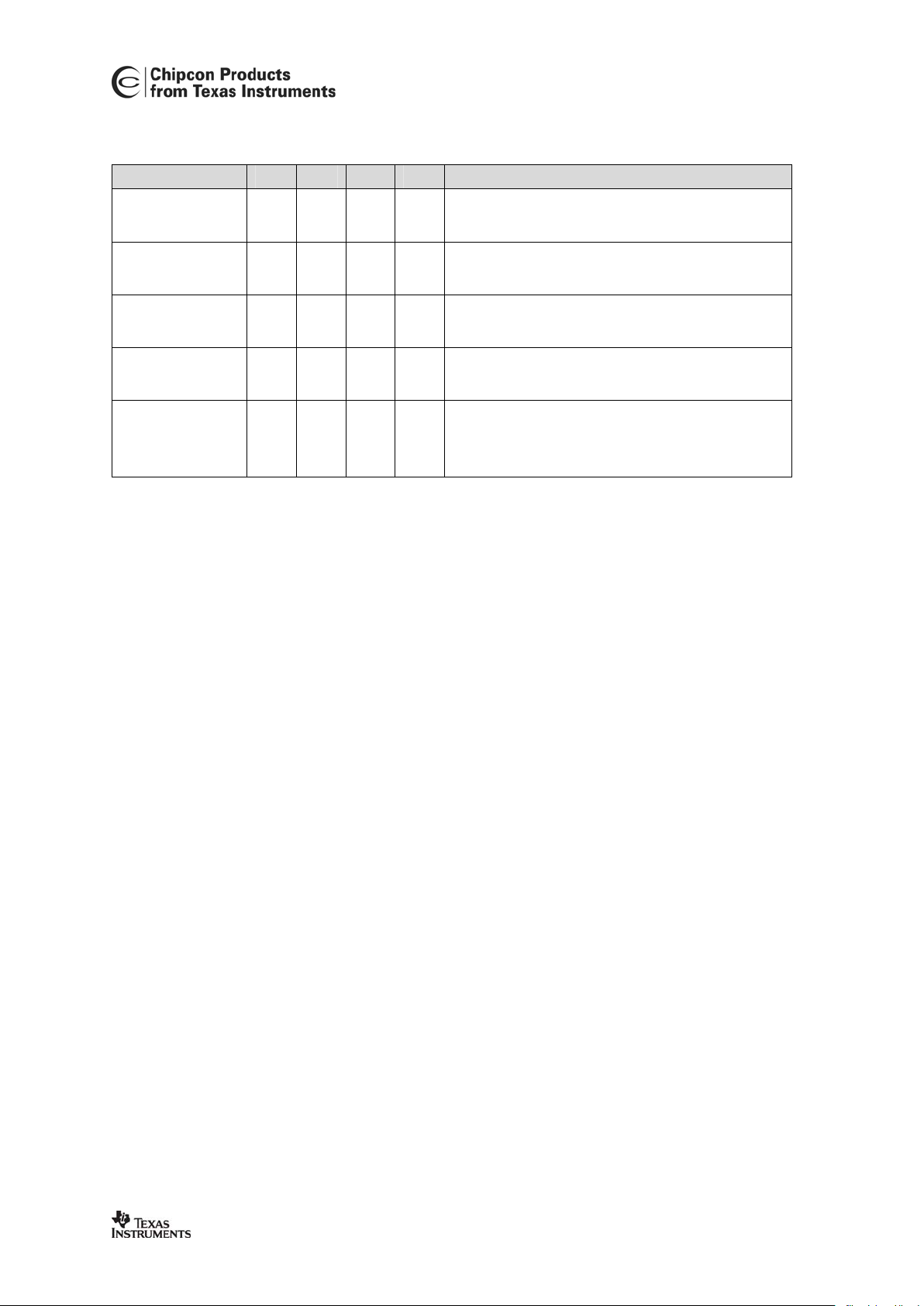
4.2 RF Receive Section
Tc = 25°C, VDD = 3.0V if nothing else stated. All measurement results are obtained using the CC1100EM reference
design.
Parameter Min Typ Max Unit Condition/Note
Digital channel filter
bandwidth
58 812 kHz User programmable. The bandwidth limits are proportional
to crystal frequency (stated values assume a 26.0 MHz
crystal).
315 MHz, 1.2 kbps data rate
(FSK, 5.2kHz deviation, 1% packet error rate, 20 bytes packet length, 58 kHz digital channel filter bandwidth)
Receiver sensitivity -111 dBm Sensitivity can be traded for current consumption by setting
MDMCFG2.DEM_DCFILT_OFF = 1. The typical current
consumption is then reduced from 17.1 mA to 15.1 mA at
sensitivity llimit. The sensitivity is typically reduced to -110
dBm
315 MHz, 500 kbps data rate
(MSK, 1% packet error rate, 20 bytes packet length, 812 kHz digital channel filter bandwidth)
-88 dBm
433 MHz, 1.2 kbps data rate
(FSK, 5.2kHz deviation, 1% packet error rate, 20 bytes packet length, 58 kHz digital channel filter bandwidth)
Receiver sensitivity –111 dBm Sensitivity can be traded for current consumption by setting
MDMCFG2.DEM_DCFILT_OFF = 1. The typical current
consumption is then reduced from 16.8 mA to 14.5 mA at
sensitivity llimit. The sensitivity is typically reduced to -109
dBm
433 MHz, 38.4 kbps data rate
(FSK, 20kHz deviation, 1% packet error rate, 20 bytes packet length, 100 kHz digital channel filter bandwidth)
Receiver sensitivity –102 dBm
433 MHz, 250 kbps data rate
(MSK, 1% packet error rate, 20 bytes packet length, 540 kHz digital channel filter bandwidth)
Receiver sensitivity –93 dBm
433 MHz, 500 kbps data rate
(MSK, 1% packet error rate, 20 bytes packet length, 812 kHz digital channel filter bandwidth)
Receiver sensitivity –88 dBm
868 MHz, 1.2 kbps data rate
(FSK, 5.2kHz deviation, 1% packet error rate, 20 bytes packet length, 58 kHz digital channel filter bandwidth)
Receiver sensitivity –111 dBm Sensitivity can be traded for current consumption by setting
MDMCFG2.DEM_DCFILT_OFF = 1. The typical current
consumption is then reduced from 17.7 mA to 15.4 mA at
sensitivity llimit. The sensitivity is typically reduced to -109
dBm
Saturation –15 dBm
Adjacent channel
rejection
32 dB Desired channel 3 dB above the sensitivity limit. 100 kHz
channel spacing
Alternate channel
rejection
33 dB Desired channel 3 dB above the sensitivity limit. 100 kHz
channel spacing
See Figure 25 for plot of selectivity versus frequency offset
Image channel
rejection,
868MHz
30 dB IF frequency 152 kHz
Desired channel 3 dB above the sensitivity limit.
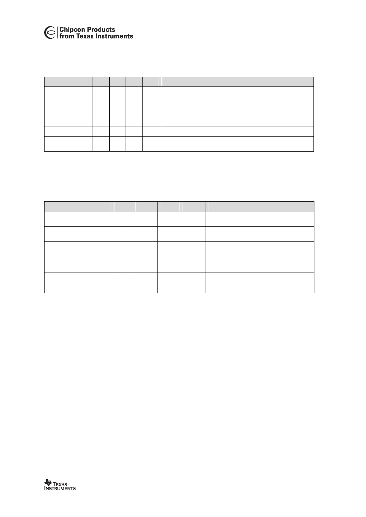
Page 11

CC1100
Data Sheet (Rev.1.1) SWRS038A Page 11 of 89
Parameter Min Typ Max Unit Condition/Note
868 MHz, 38.4 kbps data rate
(FSK, 20kHz deviation, 1% packet error rate, 20 bytes packet length, 100 kHz digital channel filter bandwidth)
Receiver sensitivity –103 dBm
Saturation –16 dBm
Adjacent channel
rejection
20 dB Desired channel 3 dB above the sensitivity limit. 200 kHz
channel spacing
Alternate channel
rejection
29 dB Desired channel 3 dB above the sensitivity limit. 200 kHz
channel spacing
See Figure 26 for plot of selectivity versus frequency offset
Image channel
rejection,
868MHz
23 dB IF frequency 152 kHz
Desired channel 3 dB above the sensitivity limit.
868 MHz, 250 kbps data rate
(MSK, 1% packet error rate, 20 bytes packet length, 540 kHz digital channel filter bandwidth)
Receiver sensitivity –93 dBm Sensitivity can be traded for current consumption by setting
MDMCFG2.DEM_DCFILT_OFF = 1. The typical current
consumption is then reduced from 17.6 mA to 15.1 mA at
sensitivity llimit. The sensitivity is typically reduced to -91
dBm
Saturation –16 dBm
Adjacent channel
rejection
24 dB Desired channel 3 dB above the sensitivity limit. 750 kHz
channel spacing
Alternate channel
rejection
38 dB Desired channel 3 dB above the sensitivity limit. 750 kHz
channel spacing
See Figure 27 for plot of selectivity versus frequency offset
Image channel
rejection,
868MHz
14 dB IF frequency 254 kHz
Desired channel 3 dB above the sensitivity limit.
868 MHz, 500 kbps data rate
(MSK, 1% packet error rate, 20 bytes packet length, 812 kHz digital channel filter bandwidth)
Receiver sensitivity –87 dBm
868 MHz, 250 kbps data rate
(OOK, 1% packet error rate, 20 bytes packet length, 540 kHz digital channel filter bandwidth)
Receiver sensitivity -88 dBm
915 MHz, 1.2 kbps data rate
(FSK, 5.2kHz deviation, 1% packet error rate, 20 bytes packet length, 58 kHz digital channel filter bandwidth)
Receiver sensitivity –111 dBm Sensitivity can be traded for current consumption by setting
MDMCFG2.DEM_DCFILT_OFF = 1. The typical current
consumption is then reduced from 17.7 mA to 15.4 mA at
sensitivity llimit. The sensitivity is typically reduced to -109
dBm
915 MHz, 38.4 kbps data rate
(FSK, 20kHz deviation, 1% packet error rate, 20 bytes packet length, 100 kHz digital channel filter bandwidth)
Receiver sensitivity –103 dBm
915 MHz, 250 kbps data rate
(MSK, 1% packet error rate, 20 bytes packet length, 540 kHz digital channel filter bandwidth)
Receiver sensitivity –93 dBm Sensitivity can be traded for current consumption by setting
MDMCFG2.DEM_DCFILT_OFF = 1. The typical current
consumption is then reduced from 17.6 mA to 15.1 mA at
sensitivity llimit. The sensitivity is typically reduced to -91
dBm
915 MHz, 500 kbps data rate
(MSK, 1% packet error rate, 20 bytes packet length, 812 kHz digital channel filter bandwidth)
Receiver sensitivity –87 dBm
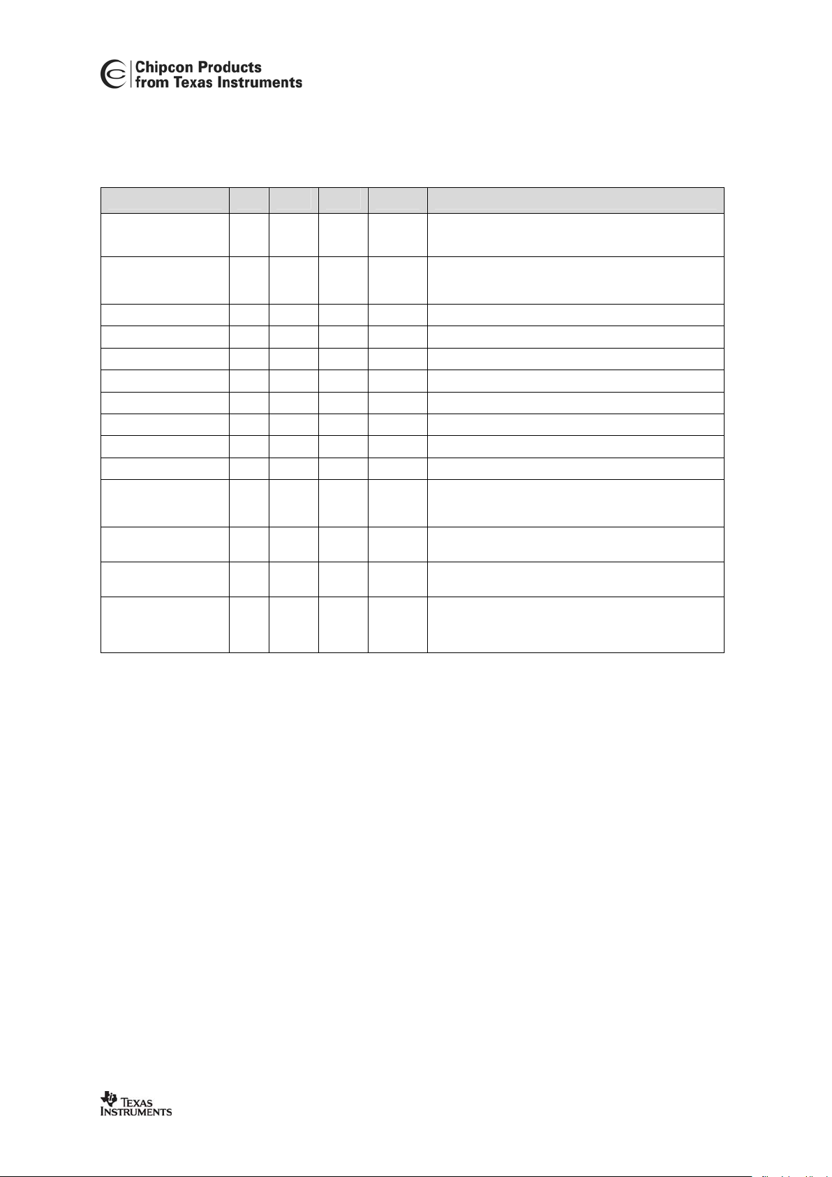
Page 12
CC1100
Data Sheet (Rev.1.1) SWRS038A Page 12 of 89
Parameter Min Typ Max Unit Condition/Note
Blocking at 2MHz
offset, 1.2 kbps,
868 MHz
-53 dBm Desired channel 3dB above the sensitivity limit. Compliant
to ETSI EN 300 220 class 2 receiver requirement.
Blocking at 2MHz
offset, 500 kbps,
868 MHz
-51 dBm Desired channel 3dB above the sensitivity limit. Compliant
to ETSI EN 300 220 class 2 receiver requirement.
Blocking at 10MHz
offset, 1.2 kbps,
868 MHz
-43 dBm Desired channel 3dB above the sensitivity limit. Compliant
to ETSI EN 300 220 class 2 receiver requirement.
Blocking at 10MHz
offset, 500 kbps,
868 MHz
-43 dBm Desired channel 3dB above the sensitivity limit. Compliant
to ETSI EN 300 220 class 2 receiver requirement.
Spurious emissions -68
-66
–57
–47
dBm
dBm
25 MHz – 1 GHz
(Maximum figure is the ETSI EN 300 220 limit)
Above 1 GHz
(Maximum figure is the ETSI EN 300 220 limit)
Table 5: RF Receive Section
Page 13

CC1100
Data Sheet (Rev.1.1) SWRS038A Page 13 of 89
4.3 RF Transmit Section
Tc = 25°C, VDD = 3.0V, +10dBm if nothing else stated. All measurement results are obtained using the CC1100EM
reference design.
Parameter Min Typ Max Unit Condition/Note
Differential load
impedance
315 MHz
433 MHz
868/915 MHz
122 + j31
116 + j41
86.5 + j43
Ω
Differential impedance as seen from the RF-port (RF_P
and RF_N) towards the antenna. Follow the CC1100EM
reference design available from theTI and Chipcon
websites.
Output power,
highest setting
10 dBm Output power is programmable, and full range is available
in all frequency bands
(Output power may be restricted by regulatory limits. See
also application note 039).
Delivered to a 50Ω single-ended load via Chipcon
reference RF matching network.
Output power,
lowest setting
-30 dBm Output power is programmable, and full range is available
in all frequency bands.
Delivered to a 50Ω single-ended load via Chipcon
reference RF matching network.
Harmonics, radiated
2
nd
Harm, 433 MHz
3
rd
Harm, 433 MHz
2
nd
Harm, 868 MHz
3
rd
Harm, 868 MHz
-50
-40
-34
-45
dBm
Measured on CC1100EM reference design with CW,
10dBm output power
The antennas used during the radiated measurements
(SMAFF-433 from R.W.Badland and Nearson
S331 868/915) plays a part in attenuating the harmonics
Harmonics,
conducted
315 MHz
433 MHz
868 MHz
915 MHz
< -33
< -38
< -51
< -34
< -32
< -31
dBm
Measured with 10dBm CW, TX frequency at 315.00 MHz,
433.00 MHz, 868.00 MHz or 915.00 MHz
Frequencies below 960 MHz
Frequencies above 960 MHz
Frequencies below 1 GHz
Frequencies above 1 GHz
Spurious emissions ,
conducted
Harmonics not
included
315 MHz
433 MHz
868 MHz
915 MHz
< -58
< -53
< -50
< -54
< -56
< -50
< -51
< -54
< -51
< -51
dBm
Measured with 10dBm CW, TX frequency at 315.00 MHz,
433.00 MHz, 868.00 MHz or 915.00 MHz
Frequencies below 960 MHz
Frequencies above 960 MHz
Frequencies below 1 GHz
Frequencies above 1 GHz
Frequencies within 47-74, 87.5-118, 174-230, 470-862
MHz
Frequencies below 1 GHz
Frequencies above 1 GHz
Frequencies within 47-74, 87.5-118, 174-230, 470-862
MHz
Frequencies below 960 MHz
Frequencies above 960 MHz
Table 6: RF Transmit Parame ters
Page 14
CC1100
Data Sheet (Rev.1.1) SWRS038A Page 14 of 89
4.4 Crystal Oscillator
Tc = 25°C @ VDD = 3.0 V if nothing else is stated.
Parameter Min Typ Max Unit Condition/Note
Crystal frequency 26 26 27 MHz
Tolerance ±40 ppm This is the total tolerance including a) initial tolerance, b) aging
and c) temperature dependence.
The acceptable crystal tolerance depends on RF frequency and
channel spacing / bandwidth.
ESR 100
Ω
Start-up time 180 µs Measured on the CC1100EM reference design. This parameter is
to a large degree crystal dependent.
Table 7: Crystal Oscillator Parameters
4.5 Low Power RC Oscillator
Tc = 25°C, VDD = 3.0 V if nothing else is stated. All measurement results obtained using the CC1100EM reference
design.
Parameter Min Typ Max Unit Condition/Note
Calibrated frequency 34.67 34.67 36 kHz Calibrated RC Oscillator frequency is XTAL
frequency divided by 750
Frequency accuracy after
calibration
±0.3 %
Temperature coefficient +0.5
% / °C
Frequency drift when temperature changes
after calibration
Supply voltage coefficient +3 % / V Frequency drift when supply voltage changes
after calibration
Initial calibration time 2 ms
When the RC Oscillator is enabled, calibration
is continuously done in the background as long
as the crystal oscillator is running.
Table 8: RC Oscillator parameters
Page 15
CC1100
Data Sheet (Rev.1.1) SWRS038A Page 15 of 89
4.6 Frequency Synthesizer Characteristics
Tc = 25°C @ VDD = 3.0 V if nothing else is stated. All measurement results are obtained using the CC1100EM reference
design.
Parameter Min Typ Max Unit Condition/Note
Programmed
frequency resolution
397 F
XOSC
/
2
16
412 Hz 26MHz-27MHz crystal.
The resolution (in Hz) is equal for all frequency bands.
Synthesizer frequency
tolerance
±40 ppm Given by crystal used. Required accuracy (including
temperature and aging) depends on frequency band and
channel bandwidth / spacing.
RF carrier phase noise –89 dBc/Hz @ 50 kHz offset from carrier
RF carrier phase noise –89 dBc/Hz @ 100 kHz offset from carrier
RF carrier phase noise –90 dBc/Hz @ 200 kHz offset from carrier
RF carrier phase noise –98 dBc/Hz @ 500 kHz offset from carrier
RF carrier phase noise –107 dBc/Hz @ 1 MHz offset from carrier
RF carrier phase noise –113 dBc/Hz @ 2 MHz offset from carrier
RF carrier phase noise –119 dBc/Hz @ 5 MHz offset from carrier
RF carrier phase noise –129 dBc/Hz @ 10 MHz offset from carrier
PLL turn-on / hop time 88.4
µs
Time from leaving the IDLE state until arriving in the RX,
FSTXON or TX state, when not performing calibration.
Crystal oscillator running.
PLL RX/TX settling
time
9.6
µs
Settling time for the 1xIF frequency step from RX to TX
PLL TX/RX settling
time
21.5
µs
Settling time for the 1xIF frequency step from TX to RX
PLL calibration time
0.69
18739
0.72
0.72
XOSC
cycles
ms
Calibration can be initiated manually, or automatically
before entering or after leaving RX/TX.
Min/typ/max time is for 27/26/26MHz crystal frequency.
Table 9: Frequency Synthe sizer Pa rameter s
Page 16
CC1100
Data Sheet (Rev.1.1) SWRS038A Page 16 of 89
4.7 Analog temperature sensor
The characteristics of the analog temperature sensor are listed in Table 10 below. Note that it is
necessary to write 0xBF to the PTEST register to use the analog temperature sensor in the IDLE
state.
Parameter Min Typ Max Unit Condition/Note
Output voltage at –40°C
0.651 V
Output voltage at 0°C
0.747 V
Output voltage at +40°C
0.847 V
Output voltage at +80°C
0.945 V
Temperature coefficient 2.45
mV/°C Fitted from –20°C to +80°C
Error in calculated
temperature, calibrated
-2
*
0 2
*
°C From –20°C to +80°C when using 2.54mV / °C,
after 1-point calibration at room temperature
*
Indicated minimum and maximum error with 1point calibration is based on simulated values for
typical process parameters
Current consumption
increase when enabled
0.3 mA
Table 10: Analog Temperature Sensor Parameters
4.8 DC Characteristics
Tc = 25°C if nothing else stated.
Digital Inputs/Outputs Min Max Unit Condition
Logic "0" input voltage 0 0.7 V
Logic "1" input voltage VDD-0.7 VDD V
Logic "0" output voltage 0 0.5 V For up to 4mA output current
Logic "1" output voltage VDD-0.3 VDD V For up to 4mA output current
Logic "0" input current N/A –50 nA Input equals 0V
Logic "1" input current N/A 50 nA Input equals VDD
Table 11: DC Characteristics
4.9 Power On Reset
When the power supply complies with the requirements in Table 12 below, proper Power-OnReset functionality is guaranteed. Otherwise, the chip should be assumed to have unknown state
until transmitting an SRES strobe over the SPI interface.
Parameter Min Typ Max Unit Condition/Note
Power-up ramp-up time. 5 ms From 0V until reaching 1.8V
Power off time 1 ms Minimum time between power-on and power-off.
Table 12: Power-on Reset Requirements
Page 17

CC1100
Data Sheet (Rev.1.1) SWRS038A Page 17 of 89
5 Pin Configuration
1
20 19 18 17 16
15
14
13
12
11
109876
5
4
3
2
GND
Exposed die
attach pad
SCLK
SO (GDO1)
GDO2
DVDD
DCOUPL
GDO0 (ATEST)
XOSC_Q1
AVDD
XOSC_Q2
AVDD
RF_P
RF_N
GND
AVDD
RBIAS
DGUARD
GND
SI
CSn
AVDD
Figure 1: Pinout top view
Note: The exposed die attach pad must be connected to a solid ground plane as this is the main
ground connection for the chip.
Page 18
CC1100
Data Sheet (Rev.1.1) SWRS038A Page 18 of 89
Pin # Pin name Pin type Description
1
SCLK
Digital Input Serial configuration interface, clock input
2
SO
(GDO1)
Digital Output Serial configuration interface, data output.
Optional general output pin when
CSn
is high
3
GDO2
Digital Output Digital output pin for general use:
• Test signals
• FIFO status signals
• Clear Channel Indicator
• Serial output RX data
4
DVDD
Power (Digital) 1.8-3.6 V digital power supply for digital I/O’s and for the digital core
voltage regulator
5
DCOUPL
Power (Digital) 1.6-2.0 V digital power supply output for decoupling.
NOTE: This pin is intended for use with the
CC1100
only. It can not be
used to provide supply voltage to other devices.
6
GDO0
(ATEST)
Digital I/O
Digital output pin for general use:
• Test signals
• FIFO status signals
• Clear Channel Indicator
• Serial output RX data
• Serial input TX data
Also used as analog test I/O for prototype/production testing
7
CSn
Digital Input Serial configuration interface, chip select
8
XOSC_Q1
Analog I/O Crystal oscillator pin 1, or external clock input
9
AVDD
Power (Analog) 1.8-3.6 V analog power supply connection
10
XOSC_Q2
Analog I/O Crystal oscillator pin 2
11
AVDD
Power (Analog) 1.8-3.6 V analog power supply connection
12
RF_P
RF I/O Positive RF input signal to LNA in receive mode
Positive RF output signal from PA in transmit mode
13
RF_N
RF I/O Negative RF input signal to LNA in receive mode
Negative RF output signal from PA in transmit mode
14
AVDD
Power (Analog) 1.8-3.6 V analog power supply connection
15
AVDD
Power (Analog) 1.8-3.6 V analog power supply connection
16
GND
Ground (Analog) Analog ground connection
17
RBIAS
Analog I/O External bias resistor for reference current
18
DGUARD
Power (Digital) Power supply connection for digital noise isolation
19
GND
Ground (Digital) Ground connection for digital noise isolation
20
SI
Digital Input Serial configuration interface, data input
Table 13: Pinout overview
Page 19
CC1100
Data Sheet (Rev.1.1) SWRS038A Page 19 of 89
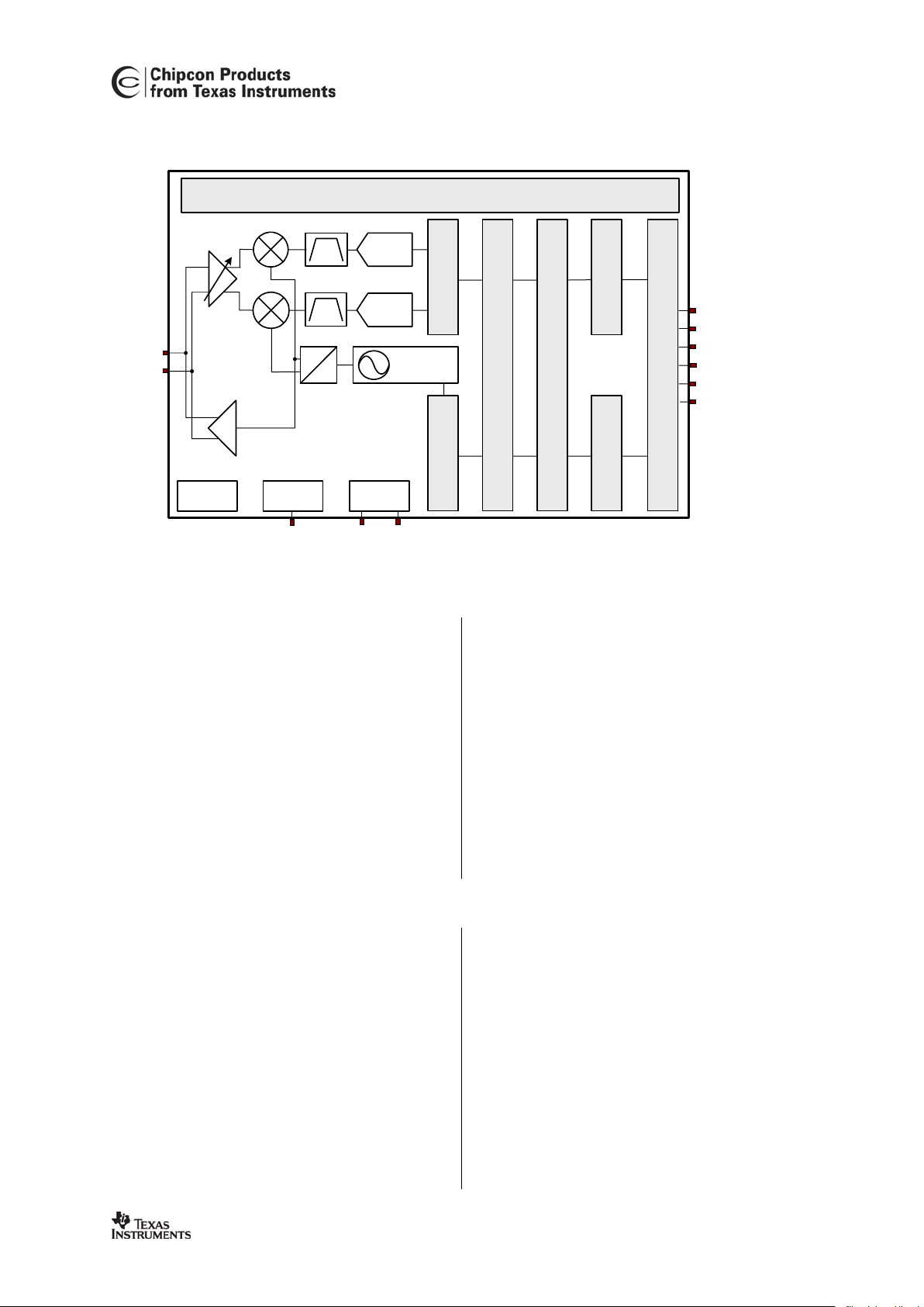
6 Circuit Description
BIAS
PA
RBI AS XOSC_Q1 XOSC_Q2
CSn
SI
SO (GDO1)
XOSC
SCLK
LNA
0
90
FREQ
SYNTH
ADC
ADC
DEMODULATOR
FEC / INTERLEAVER
PACKET HANDLER
RXFIFO
MODULATOR
TXFIFO
DIGITAL INTERFACE TO MCU
RADIO CONTROL
RF_P
RF_N
GDO2
GDO0 (ATEST)
RC OSC
Figure 2:
CC1100
Simplified Block Dia gram
A simplified block diagram of
CC1100
is shown
in Figure 2.
CC1100
features a low-IF receiver. The
received RF signal is amplified by the lownoise amplifier (LNA) and down-converted in
quadrature (I and Q) to the intermediate
frequency (IF). At IF, the I/Q signals are
digitised by the ADCs. Automatic gain control
(AGC), fine channel filtering and demodulation
bit/packet synchronization are performed
digitally.
The transmitter part of
CC1100
is based on
direct synthesis of the RF frequency. The
frequency synthesizer includes a completely
on-chip LC VCO and a 90 degree phase
shifter for generating the I and Q LO signals to
the down-conversion mixers in receive mode.
A crystal is to be connected to XOSC_Q1 and
XOSC_Q2. The crystal oscillator generates the
reference frequency for the synthesizer, as
well as clocks for the ADC and the digital part.
A 4-wire SPI serial interface is used for
configuration and data buffer access.
The digital baseband includes support for
channel configuration, packet handling and
data buffering.
7 Application Circuit
Only a few external components are required
for using the
CC1100
. The recommended
application circuits are shown in Figure 3 and
Figure 4. The external components are
described in Table 14, and typical values are
given in Table 15.
Bias resistor
The bias resistor R171 is used to set an
accurate bias current reference.
Balun and RF matching
The components between the RF_N/RF_P
pins and the point where the two signals are
joined together (C131, C121, L121 and L131
for the 315/433 MHz desgn. L121, L131,
C121, L122, C131, C122 and L132 for the
868/915 MHz reference design) form a balun
that converts the differential RF signal on
CC1100
to a single-ended RF signal (C124 is
also needed for DC blocking). Together with
an appropriate LC network, the balun
components also transform the impedance to
match a 50Ω antenna (or cable). Suggested
values for 315MHz, 433MHz and 868/915MHz
are listed in Table 15.
The balun and LC filter component values and
their placement are important to achieve
Page 20
CC1100
Data Sheet (Rev.1.1) SWRS038A Page 20 of 89
optimal performance. It is highly
recommended to follow the CC1100EM
reference design.
Crystal
The crystal oscillator uses an external crystal
with two loading capacitors (C81 and C101).
See section 25 on page 49 for details.
Additional filtering
Additional external components (e.g. an RF
SAW filter) may be used in order to improve
the performance in specific applications.
Power supply decoupling
The power supply must be properly decoupled
close to the supply pins. Note that decoupling
capacitors are not shown in the application
circuit. The placement and the size of the
decoupling capacitors are very important to
achieve the optimum performance. The
CC1100EM reference design should be
followed closely.
Component Description
C51 100nF decoupling capacitor for on-chip voltage regulator to digital part
C81/C101 Crystal loading capacitors, see section 25 on page 49 for details
C121/C131 RF balun/matching capacitors
C122 RF LC filter/matching filter capacitor (315 and 433 MHz). RF balun/matching
capacitor (868/915 MHz).
C123 RF LC filter/matching capacitor
C124 RF balun DC blocking capacitor
C125 RF LC filter DC blocking capacitor (only needed if there is a DC path in the antenna)
L121/L131 RF balun/matching inductors (inexpensive multi-layer type)
L122 RF LC filter/matching filter inductor (315 and 433 MHz). RF balun/matching inductor
(868/915 MHz). (inexpensive multi-layer type)
L123 RF LC filter/matching filter inductor (inexpensive multi-layer type)
L132 RF balun/matching inductor. (inexpensive multi-layer type)
R171 56kΩ resistor for internal bias current reference. 1% tolerance
XTAL 26MHz-27MHz crystal, see section 25 on page 49 for details
Table 14: Overview of external components (excluding supply decoupling capacitors)
Page 21
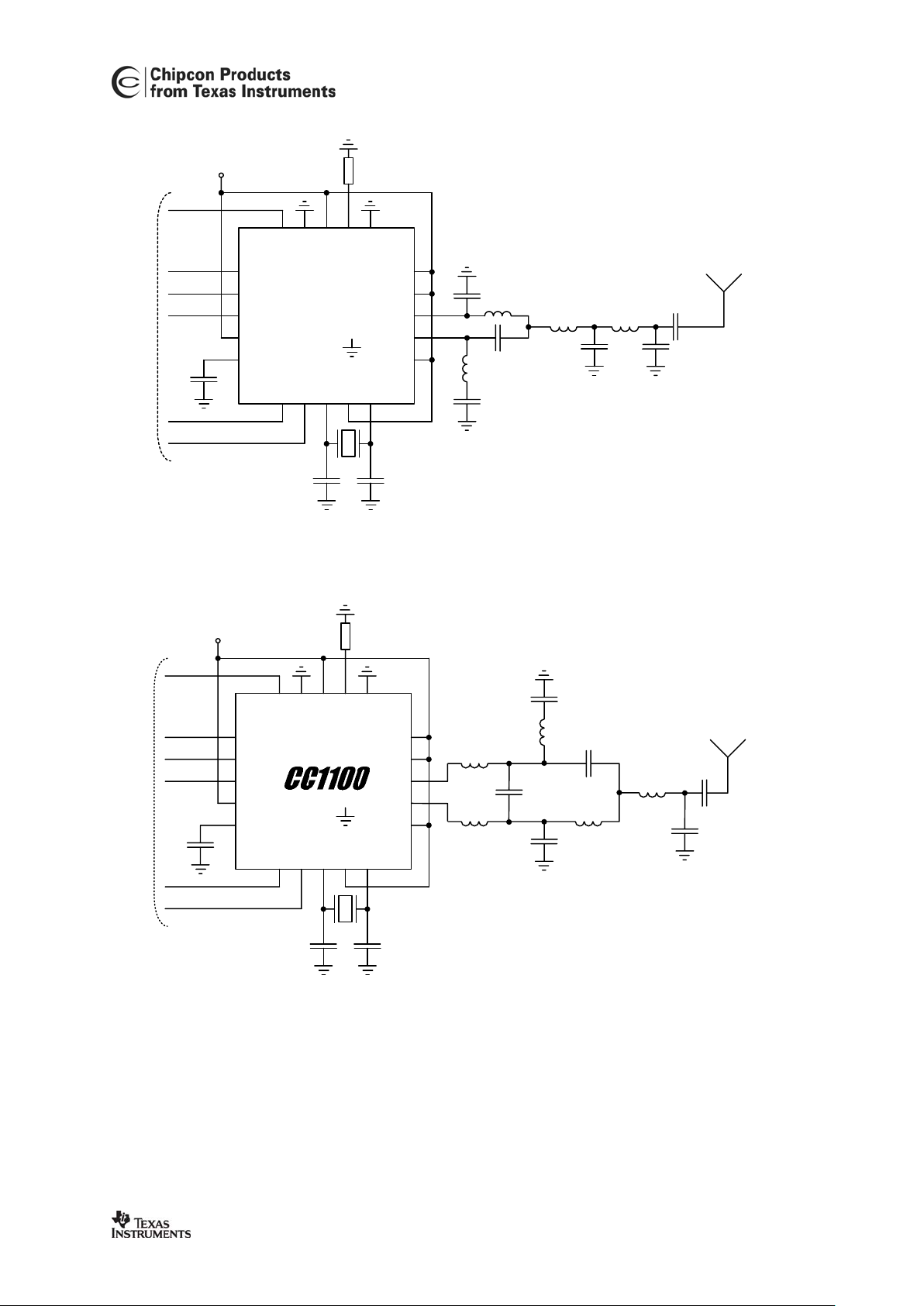
CC1100
Data Sheet (Rev.1.1) SWRS038A Page 21 of 89
Antenna
(50 Ohm)
Digital Inteface
1.8V-3.6V power supply
6 GDO0
7 CSn
8 XOSC_Q1
9 AVDD
10 XOSC_Q2
SI 20
GND 19
DGUARD 18
RBIAS 17
GND 16
1 SCLK
2 SO
(GDO1)
3 GDO2
4 DVDD
5 DCOUPL
AVDD 15
AVDD 14
RF_N 13
RF_P 12
AVDD 11
XTAL
L122 L123
C122 C123
C125
R171
C81 C101
C51
CSn
GDO0
(optional)
GDO2
(optional)
SO
(GDO1)
SCLK
SI
CC1100
DIE ATTACH PAD:
C131
C121
L121
L131
C124
Figure 3: Typical application and evaluation circuit 315/433 MHz (excluding supply decoupling
capacitors)
Antenna
(50 Ohm)
Digital Inteface
1.8V-3.6V power supply
6 GDO0
7 CSn
8 XOSC_Q1
9 AVDD
10 XOSC_Q2
SI 20
GND 19
DGUARD 18
RBIAS 17
GND 16
1 SCLK
2 SO (GDO1)
3 GDO2
4 DVDD
5 DCOUPL
AVDD 15
AVDD 14
RF_N 13
RF_P 12
AVDD 11
XTAL
C121
C122
L122
L132
C124
L131
L123
C125
R171
C81 C101
C51
CSn
GDO0
(optional)
GDO2
(optional)
SO
(GDO1)
SCLK
SI
DIE ATTACH PAD:
L121
C131
C123
Figure 4: Typical application and evaluation circuit 868/915 MHz (excluding supply
decoupling capacitors)
Page 22
CC1100
Data Sheet (Rev.1.1) SWRS038A Page 22 of 89
Component Value at 315MHz
Value at 433MHz Value at 868/915MHz
C51 100nF±10%, 0402 X5R
C81 27pF±5%, 0402 NP0
C101 27pF±5%, 0402 NP0
C121 6.8pF±0.5pF, 0402 NP0 3.9pF±0.25pF, 0402 NP0 1.0pF±0.25pF, 0402 NP0
C122 12pF±5%, 0402 NP0 8.2pF±0.5pF, 0402 NP0 1.5pF±0.25pF, 0402 NP0
C123 6.8pF±0.5pF, 0402 NP0 5.6pF±0.5pF, 0402 NP0 1.8pF±0.25pF, 0402 NP0
C124 220pF±5%, 0402 NP0 220pF±5%, 0402 NP0 100pF±5%, 0402 NP0
C125 220pF±5%, 0402 NP0 220pF±5%, 0402 NP0 100pF±5%, 0402 NP0
C131 6.8pF±0.5pF, 0402 NP0 3.9pF±0.25pF, 0402 NP0 1.5pF±0.25pF, 0402 NP0
L121 33nH±5%, 0402 monolithic 27nH±5%, 0402 monolithic 12nH±5%, 0402 monolithic
L122 18nH±5%, 0402 monolithic 22nH±5%, 0402 monolithic 18nH±5%, 0402 monolithic
L123 33nH±5%, 0402 monolithic 27nH±5%, 0402 monolithic 6.2nH±5%, 0402 monolithic
L131 33nH±5%, 0402 monolithic 27nH±5%, 0402 monolithic 12nH±5%, 0402 monolithic
L132 18nH±5%, 0402 monolithic
R171 56kΩ±1%, 0402
XTAL 26.0MHz surface mount crystal
Table 15: Bill Of Materials for the application circuit
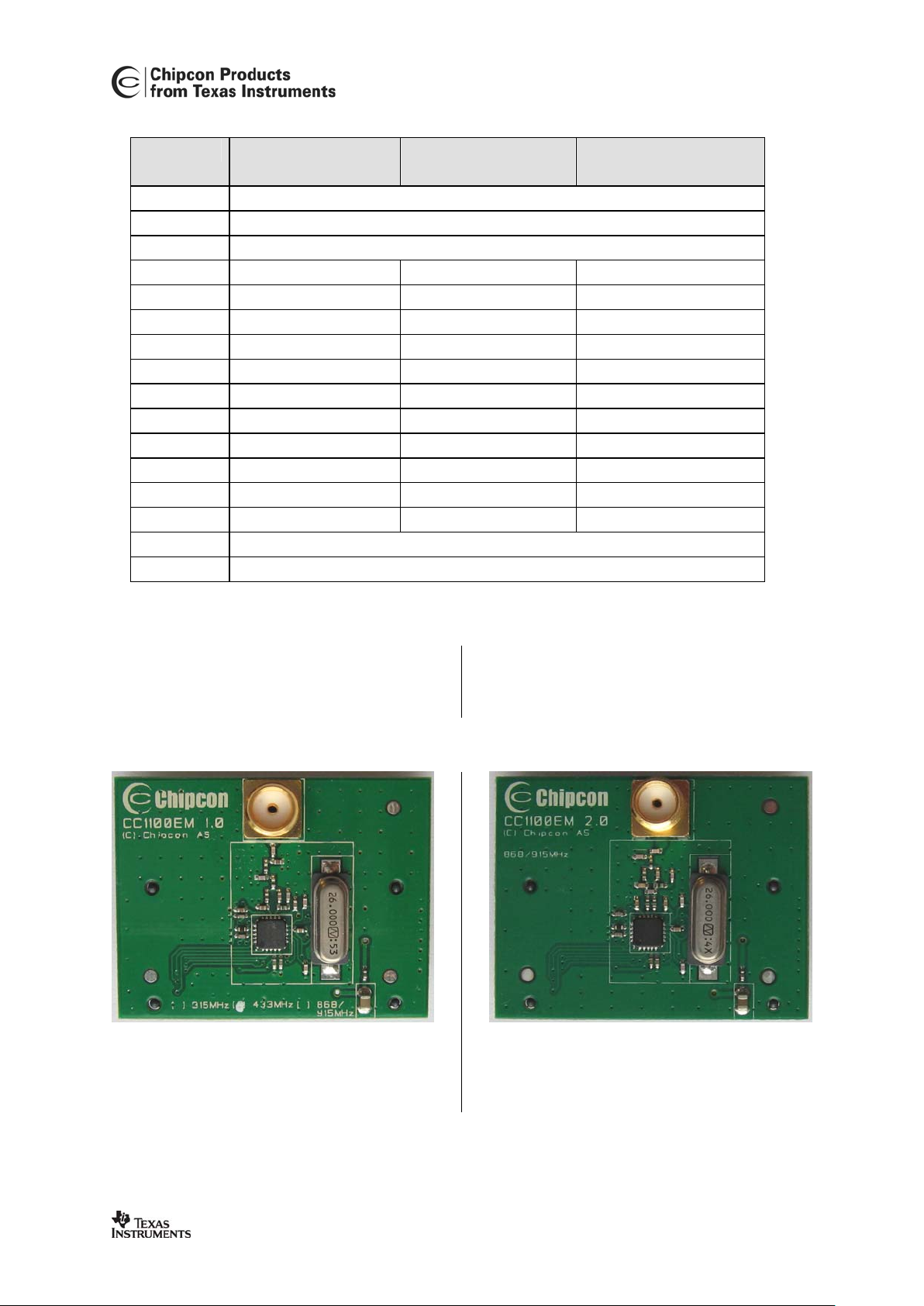
In the CC1100EM reference designs shown in
Figure 5 and Figure 6, LQG-15HS series
inductors and GRM1555C series capacitors
from Murata have been used.
The Gerber files for the CC1100EM reference
designs are available from the TI and Chipcon
websites.
Figure 5: CC1100EM reference design, 433
MHz. Same PCB is used for 315 MHz
Figure 6: CC1100EM reference design,
868/915 MHz
Page 23
CC1100
Data Sheet (Rev.1.1) SWRS038A Page 23 of 89
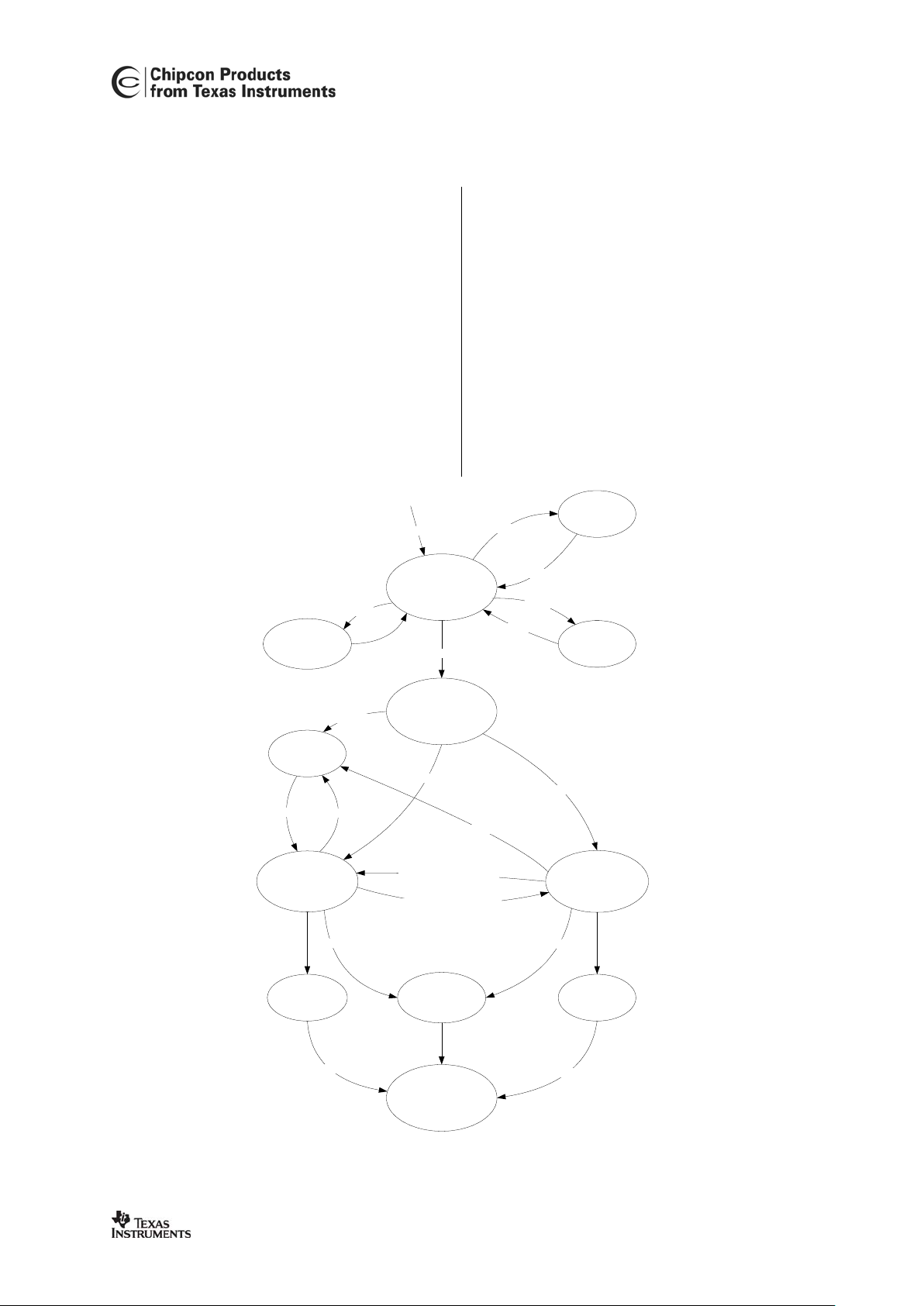
8 Configuration Overview
CC1100
can be configured to achieve optimum
performance for many different applications.
Configuration is done using the SPI interface.
The following key parameters can be
programmed:
• Power-down / power up mode
• Crystal oscillator power-up / power-down
• Receive / transmit mode
• RF channel selection
• Data rate
• Modulation format
• RX channel filter bandwidth
• RF output power
• Data buffering with separate 64-byte
receive and transmit FIFOs
• Packet radio hardware support
• Forward Error Correction with interleaving
• Data Whitening
• Wake-On-Radio (WOR)
Details of each configuration register can be
found in section 31, starting on page 56.
Figure 7 shows a simplified state diagram that
explains the main
CC1100
states, together with
typical usage and current consumption. For
detailed information on controlling the
CC1100
state machine, and a complete state diagram,
see section 19, starting on page 41.
Transmit mode Receive mode
IDLE
Manual freq.
synth. calibration
RX FIFO
overflow
TX FIFO
underflow
Frequency
synthesizer on
SFSTXON
SRX or wake-on-radio (WOR)
STX
STX
STX or RXOFF_MODE=10
RXOFF_MODE=00
SFTX
SRX or TXOFF_MODE=11
SIDLE
SCAL
SFRX
IDLE
TXOFF_MODE=00
SFSTXON or RXOFF_MODE=01
SRX or STX or SFSTXON or wake-on-radio (WOR)
Sleep
SPWD or w ake-on-radio (WO R)
Crystal
oscillator off
SXOFF
CSn=0
CSn=0
TXOFF_MODE=01
Frequency
synthesizer startup,
optional calibration,
settling
Optiona l freq.
synth. calibration
Default state when the radio is not
receiving or transmitting. Typ.
current consumption: 1.6mA.
Lowest power mode. Most
register values are retained.
Current consumption typ
400nA, or typ 900nA when
wake-on -radio (W OR) is
enabled.
All register values are
retained. Typ. current
consumption; 0.16mA.
Used for calibrating frequency
synthesizer upfront (entering
receive or transmit mode can
then be done quicker).
Transitional state. Typ. current
consumption: 8.2mA.
Frequency synthesizer is turned on, can optionally be
calibrated, and then settles to the correct frequency.
Transitional state. Typ. current consumption: 8.2mA.
Frequency synthesizer is on,
ready to s tart transm itting.
Transmission starts very
quickly after receiving the
STX command strobe.Typ.
current consumption: 8.2mA.
Typ. current consumption:
13.5mA at -6dBm output,
16.5mA at 0dBm output,
30mA at +10dBm output.
Typ. current
consumption:
from 14.4mA (strong
input signal) to 15.4mA
(weak input signal) at
1.2kbps.
Optional transitional state. Typ.
current consumption: 8.2mA.
In FIFO-based modes,
transmission is turned off
and this state entered if the
TX FIFO becomes empty in
the middle of a packet. Typ.
current consumption: 1.6mA.
In FIFO-based modes,
reception is turned off and
this state entered if the RX
FIFO overflows. Typ.
current consumption:
1.6mA.
Figure 7: Simplified state diagram, with typical usage and current consumption
Page 24

CC1100
Data Sheet (Rev.1.1) SWRS038A Page 24 of 89
9 Configuration Software
CC1100
can be configured using the SmartRF®
Studio software, available for download from
http://www.chipcon.com or www.ti.com/lpw.
The SmartRF
®
Studio software is highly
recommended for obtaining optimum register
settings, and for evaluating performance and
functionality. A screenshot of the SmartRF
®
Studio user interface for
CC1100
is shown in
Figure 8.
Figure 8: SmartRF
®
Studio user interface
10 4-wire Serial Configuration and Data Interface
CC1100
is configured via a simple 4-wire SPI-
compatible interface (SI, SO, SCLK and CSn)
where
CC1100
is the slave. This interface is
also used to read and write buffered data. All
address and data transfer on the SPI interface
is done most significant bit first.
All transactions on the SPI interface start with
a header byte containing a read/write bit, a
burst access bit and a 6-bit address.
During address and data transfer, the CSn pin
(Chip Select, active low) must be kept low. If
CSn goes high during the access, the transfer
will be cancelled. The timing for the address
and data transfer on the SPI interface is shown
in Figure 9 with reference to Table 16.
When CSn goes low, the MCU must wait until
CC1100
SO pin goes low before starting to
transfer the header byte. This indicates that
the voltage regulator has stabilized and the
crystal is running. Unless the chip was in the
SLEEP or XOFF states, the SO pin will always
go low immediately after taking CSn low.
Figure 10 gives a brief overview of different
register access types possible.
Page 25
CC1100
Data Sheet (Rev.1.1) SWRS038A Page 25 of 89
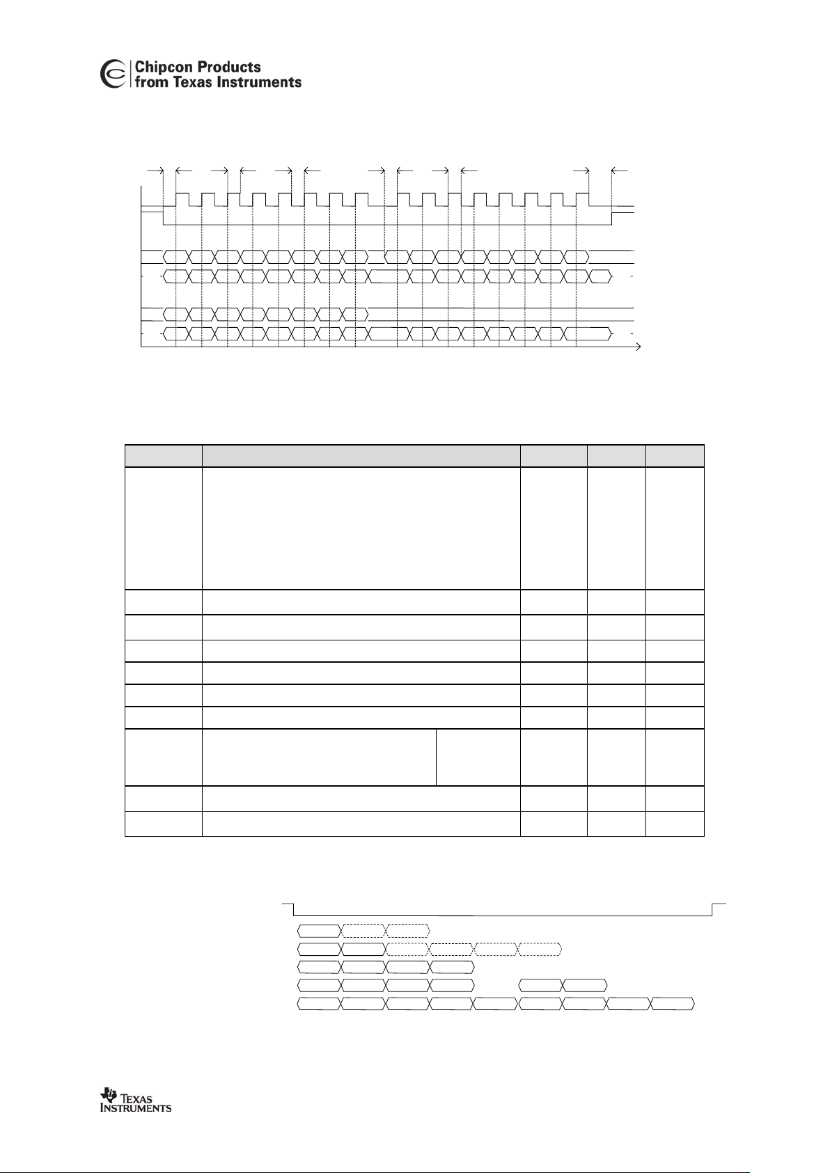
0
A6 A5 A4 A3 A2
A0A1
DW7 DW6 DW5 DW4 DW3 DW2 DW1 DW0
1
A6 A5 A4 A3 A2
A0A1
DR7 DR6 DR5 DR4 DR3 DR2 DR1 D
R
0
Read from register:
Write to register:
Hi-Z
X
SCLK:
CSn:
SI
SO
SI
SO
Hi-Z
t
sp
t
ch
t
cl
t
sd
t
hd
t
ns
X
X
Hi-Z
X
S7 S 6 S 5 S4 S 3 S 2 S 1 S0
Hi-Z
S7 S 6 S 5 S4 S 3 S 2 S 1 S0 S7 S6 S5 S4 S3 S 2 S1 S0 S7
X
Figure 9: Configuration registers write and read operations
Parameter Description Min Max Units
SCLK
frequency
100 ns delay inserted between address byte and data byte (single access), or
between address and data, and between each data byte (burst access).
- 10
SCLK
frequency, single access
No delay between address and data byte
- 9
f
SCLK
SCLK
frequency, burst access
No delay between address and data byte, or between data bytes
- 6.5
MHz
t
sp,pd
CSn
low to positive edge on
SCLK
, in power-down mode
200 -
µs
tsp
CSn
low to positive edge on
SCLK
, in active mode
20 - ns
tch Clock high 50 - ns
tcl Clock low 50 - ns
t
rise
Clock rise time - 5 ns
t
fall
Clock fall time - 5 ns
tsd Setup data (negative SCLK edge) to
positive edge on
SCLK
(tsd applies between address and data bytes, and between
data bytes)
Single access
Burst access
55
76
-
-
ns
thd
Hold data after positive edge on
SCLK
20 - ns
tns
Negative edge on
SCLK
to
CSn
high.
20 - ns
Table 16: SPI interface timing requirements
DATA
byte 0
A
DDR
FIFO
DATA
byte 1
DATA
byte 2
DATA
byte n-1
DATA
byte n
...
A
DDR
strobe
DATA
A
DDR
strobe
A
DDR
reg
A
DDR
reg n
DATAnDATA
n+1
DATA
n+2
...
A
DDR
strobe
...
CSn:
Command strobe(s):
Read or write register(s):
ead or write consecutive register s (burst):
DATA
A
DDR
reg
DATA
A
DDR
reg
...
DATA
byte 0
A
DDR
FIFO
DATA
byte 1
Combinations:
DATA
A
DDR
reg
DATA
A
DDR
reg
A
DDR
strobe
A
DDR
strobe
...
Read or write n+1 bytes from/to RF FIFO:
Figure 10: Register access types
Page 26
CC1100
Data Sheet (Rev.1.1) SWRS038A Page 26 of 89
10.1 Chip Status Byte
When the header byte, data byte or command
strobe is sent on the SPI interface, the chip
status byte is sent by the
CC1100
on the SO pin.
The status byte contains key status signals,
useful for the MCU. The first bit, s7, is the
CHIP_RDYn signal; this signal must go low
before the first positive edge of SCLK. The
CHIP_RDYn signal indicates that the crystal is
running and the regulated digital supply
voltage is stable.
Bits 6, 5 and 4 comprises the STATE value.
This value reflects the state of the chip. The
XOSC and power to the digital core is on in the
IDLE state, but all other modules are in power
down. The frequency and channel
configuration should only be updated when the
chip is in this state. The RX state will be active
when the chip is in receive mode. Likewise, TX
is active when the chip is transmitting.
The last four bits (3:0) in the status byte contains FIFO_BYTES_AVAILABLE. For read
operations, the FIFO_BYTES_AVAILABLE
field contains the number of bytes available for
reading from the RX FIFO. For write
operations, the FIFO_BYTES_AVAILABLE
field contains the number of bytes free for
writing into the TX FIFO. When
FIFO_BYTES_AVAILABLE=15, 15 or more
bytes are available/free.
Table 17 gives a status byte summary.
Bits Name Description
7 CHIP_RDYn Stays high until power and crystal have stabilized. Should always be low when using
the SPI interface.
6:4 STATE[2:0] Indicates the current main state machine mode
Value State Description
000 Idle IDLE state
(Also reported for some transitional states instead
of SETTLING or CALIBRATE, due to a small error)
001 RX Receive mode
010 TX Transmit mode
011 FSTXON Fast TX ready
100 CALIBRATE Frequency synthesizer calibration is running
101 SETTLING PLL is settling
110 RXFIFO_OVERFLOW RX FIFO has overflowed. Read out any
useful data, then flush the FIFO with
SFRX
111 TXFIFO_UNDERFLOW TX FIFO has underflowed. Acknowledge with
SFTX
3:0 FIFO_BYTES_AVAILABLE[3:0] The number of bytes available in the RX FIFO or free bytes in the TX FIFO
(depends on the read/write-bit). If FIFO_BYTES_AVAILABLE=15, it indicates that
15 or more bytes are available/free.
Table 17: Status byte summary
10.2 Register Access
The configuration registers on the
CC1100
are
located on SPI addresses from 0x00 to 0x2F.
Table 35 on page 58 lists all configuration
registers. The detailed description of each
register is found in Section 31.1, starting on
page 61. All configuration registers can be
both written to and read. The read/write bit
controls if the register should be written to or
read. When writing to registers, the status byte
is sent on the SO pin each time a header byte
or data byte is transmitted on the SI pin.
When reading from registers, the status byte is
Page 27
CC1100
Data Sheet (Rev.1.1) SWRS038A Page 27 of 89
sent on the SO pin each time a header byte is
transmitted on the SI pin.
Registers with consecutive addresses can be
accessed in an efficient way by setting the
burst bit in the address header. The address
sets the start address in an internal address
counter. This counter is incremented by one
each new byte (every 8 clock pulses). The
burst access is either a read or a write access
and must be terminated by setting CSn high.
For register addresses in the range 0x300x3D, the “burst” bit is used to select between
status registers and command strobes (see
below). The status registers can only be read.
Burst read is not available for status registers,
so they must be read one at a time.
10.3 SPI Read
When reading register fields over the SPI
interface while the register fields are updated
by the radio hardware (e.g. MARCSTATE or
TXBYTES), there is a small, but finite,
probability that a single read from the register
being corrupt. As an example, the probability
of any single read from TXBYTES being
corrupt, assuming the maximum data rate is
used, is approximately 80 ppm. Refer to the
CC1100
Errata Note for more details.
10.4 Command Strobes
Command Strobes may be viewed as single
byte instructions to
CC1100
. By addressing a
Command Strobe register, internal sequences
will be started. These commands are used to
disable the crystal oscillator, enable receive
mode, enable wake-on-radio etc. The 14
command strobes are listed in Table 34 on
page 57.
The command strobe registers are accessed
in the same way as for a register write
operation, but no data is transferred. That is,
only the R/W bit (set to 0), burst access (set to
0) and the six address bits (in the range 0x30
through 0x3D) are written.
When writing command strobes, the status
byte is sent on the SO pin.
A command strobe may be followed by any
other SPI access without pulling CSn high.
After issuing an SRES command strobe the
next command strobe can be issued when the
SO pin goes low as shown in Figure 11 The
command strobes are executed immediately,
with the exception of the SPWD and the SXOFF
strobes that are executed when CSn goes
high.
Figure 11: SRES command strobe
10.5 FIFO Access
The 64-byte TX FIFO and the 64-byte RX
FIFO are accessed through the 0x3F address.
When the read/write bit is zero, the TX FIFO is
accessed, and the RX FIFO is accessed when
the read/write bit is one.
The TX FIFO is write-only, while the RX FIFO
is read-only.
The burst bit is used to determine if FIFO
access is single byte or a burst access. The
single byte access method expects address
with burst bit set to zero and one data byte.
After the data byte a new address is expected;
hence, CSn can remain low. The burst access
method expects one address byte and then
consecutive data bytes until terminating the
access by setting CSn high.
The following header bytes access the FIFOs:
• 0x3F: Single byte access to TX FIFO
• 0x7F: Burst access to TX FIFO
• 0xBF: Single byte access to RX FIFO
• 0xFF: Burst access to RX FIFO
When writing to the TX FIFO, the status byte
(see Section 10.1) is output for each new data
byte on SO, as shown in Figure 9. This status
byte can be used to detect TX FIFO underflow
while writing data to the TX FIFO. Note that
the status byte contains the number of bytes
free before writing the byte in progress to the
TX FIFO. When the last byte that fits in the TX
FIFO is transmitted to the SI pin, the status
byte received concurrently on the SO pin will
indicate that one byte is free in the TX FIFO.
The transmit FIFO may be flushed by issuing a
SFTX command strobe. Similarly, a SFRX
command strobe will flush the receive FIFO. A
SFTX or SFRX command strobe can only be
issued in the IDLE, TXFIFO_UNDERLOW or
Page 28

CC1100
Data Sheet (Rev.1.1) SWRS038A Page 28 of 89
RXFIFO_OVERFLOW state. Both FIFOs are
flushed when going to the SLEEP state.
10.6 PATABLE Access
The 0x3E address is used to access the
PATABLE, which is used for selecting PA
power control settings. The SPI expects up to
eight data bytes after receiving the address.
By programming the PATABLE, controlled PA
power ramp-up and ramp-down can be
achieved, as well as ASK modulation shaping
for reduced bandwidth. Note that the ASK
modulation shaping is limited to output powers
below -1 dBm, and the PATABLE settings
allowed for ASK is 0x30 to 0x3F. See
SmartRF
®
Studio for recommended shaping
sequence.
See section 24 on page 48 for details on
output power programming.
The PATABLE is an 8-byte table that defines
the PA control settings to use for each of the
eight PA power values (selected by the 3-bit
value FREND0.PA_POWER). The table is
written and read from the lowest setting (0) to
the highest (7), one byte at a time. An index
counter is used to control the access to the
table. This counter is incremented each time a
byte is read or written to the table, and set to
the lowest index when CSn is high. When the
highest value is reached the counter restarts at
zero.
The access to the PATABLE is either single
byte or burst access depending on the burst
bit. When using burst access the index counter
will count up; when reaching 7 the counter will
restart at 0. The read/write bit controls whether
the access is a write access (R/W=0) or a read
access (R/W=1).
If one byte is written to the PATABLE and this
value is to be read out then CSn must be set
high before the read access in order to set the
index counter back to zero.
Note that the content of the PATABLE is lost
when entering the SLEEP state, except for the
first byte (index 0).
11 Microcontroller Interface and Pin Configuration
In a typical system,
CC1100
will interface to a
microcontroller. This microcontroller must be
able to:
• Program
CC1100
into different modes,
• Read and write buffered data
• Read back status information via the 4-wire
SPI-bus configuration interface (SI, SO,
SCLK and CSn).
11.1 Configuration Interface
The microcontroller uses four I/O pins for the
SPI configuration interface (SI, SO, SCLK and
CSn). The SPI is described in Section 10 on
page 24.
11.2 General Control and Status Pins
The
CC1100
has two dedicated configurable
pins and one shared pin that can output
internal status information useful for control
software. These pins can be used to generate
interrupts on the MCU. See Section 28 page
52 for more details on the signals that can be
programmed. The dedicated pins are called
GDO0 and GDO2. The shared pin is the SO pin
in the SPI interface. The default setting for
GDO1/SO is 3-state output. By selecting any
other of the programming options the
GDO1/SO pin will become a generic pin. When
CSn is low, the pin will always function as a
normal SO pin.
In the synchronous and asynchronous serial
modes, the GDO0 pin is used as a serial TX
data input pin while in transmit mode.
The GDO0 pin can also be used for an on-chip
analog temperature sensor. By measuring the
voltage on the GDO0 pin with an external ADC,
the temperature can be calculated.
Specifications for the temperature sensor are
found in section 4.7 on page 16.
With default PTEST register setting (0x7F) the
temperature sensor output is only available
when the frequency synthesizer is enabled
(e.g. the MANCAL, FSTXON, RX and TX
states). It is necessary to write 0xBF to the
PTEST register to use the analog temperature
sensor in the IDLE state. Before leaving the
IDLE state, the PTEST register should be
restored to its default value (0x7F).
Page 29

CC1100
Data Sheet (Rev.1.1) SWRS038A Page 29 of 89
11.3 Optional radio control feature
The
CC1100
has an optional way of controlling
the radio, by reusing SI, SCLK and CSn from
the SPI interface. This feature allows for a
simple three-pin control of the major states of
the radio: SLEEP, IDLE, RX and TX.
This optional functionality is enabled with the
MCSM0.PIN_CTRL_EN configuration bit.
State changes are commanded as follows
when CSn is high the SI and SCLK is set to
the desired state according to Table 18. When
CSn goes low the state of SI and SCLK is
latched and a command strobe is generated
internally according to the pin configuration. It
is only possible to change state with this
functionality. That means that for instance RX
will not be restarted if SI and SCLK are set to
RX and CSn toggles. When CSn is low the SI
and SCLK has normal SPI functionality.
All pin control command strobes are executed
immediately, except the SPWD strobe, which is
delayed until CSn goes high.
CSn
SCLK
SI
Function
1 X X
Chip unaffected by SCLK/
SI
↓
0 0
Generates
SPWD
strobe
↓
0 1
Generates
STX
strobe
↓
1 0
Generates
SIDLE
strobe
↓
1 1
Generates
SRX
strobe
0
SPI
mode
SPI
mode
SPI mode (wakes up into
IDLE if in SLEEP/XOFF)
Table 18: Optional pin c ontro l coding
12 Data Rate Programming
The data rate used when transmitting, or the
data rate expected in receive is programmed
by the MDMCFG3.DRATE_M and the
MDMCFG4.DRATE_E configuration registers.
The data rate is given by the formula below.
As the formula shows, the programmed data
rate depends on the crystal frequency.
()
XOSC
EDRATE
DATA
f
MDRATE
R ⋅
⋅+
=
28
_
2
2_256
The following approach can be used to find
suitable values for a given data rate:
256
2
2
_
2
log_
_
28
20
2
−
⋅
⋅
=
⎥
⎥
⎦
⎥
⎢
⎢
⎣
⎢
⎟
⎟
⎠
⎞
⎜
⎜
⎝
⎛
⋅
=
EDRATE
XOSC
DATA
XOSC
DATA
f
R
MDRATE
f
R
EDRATE
If DRATE_M is rounded to the nearest integer
and becomes 256, increment DRATE_E and
use DRATE_M=0.
The data rate can be set from 1.2 kbps to 500
kbps with the minimum step size of:
Min Data
rate
[kbps]
Typical data
rate
[kbps]
Max Data
rate
[kbps]
Data rate
step size
[kbps]
0.8 1.2 / 2.4 3.17 0.0062
3.17 4.8 6.35 0.0124
6.35 9.6 12.7 0.0248
12.7 19.6 25.4 0.0496
25.4 38.4 50.8 0.0992
50.8 76.8 101.6 0.1984
101.6 153.6 203.1 0.3967
203.1 250 406.3 0.7935
406.3 500 500 1.5869
Table 19: Data rate step size
13 Receiver Channel Filter Bandwidth
In order to meet different channel width
requirements, the receiver channel filter is
programmable. The MDMCFG4.CHANBW_E and
MDMCFG4.CHANBW_M configuration registers
control the receiver channel filter bandwidth,
which scales with the crystal oscillator
Page 30

CC1100
Data Sheet (Rev.1.1) SWRS038A Page 30 of 89
frequency. The following formula gives the
relation between the register settings and the
channel filter bandwidth:
ECHANBW
XOSC
channel
MCHANBW
f
BW
_
2)·_4(8 +⋅
=
The
CC1100
supports the following channel
filter bandwidths:
MDMCFG4.CHANBW_E Channel filter
bandwidth
[kHz]
00 01 10 11
00 812 406 203 102
01 650 325 162 81
10 541 270 135 68
MDMCFG4.
CHANBW_M
11 464 232 116 58
Table 20: Channel filter bandwidths
(assuming a 26MHz crystal)
For best performance, the channel filter
bandwidth should be selected so that the
signal bandwidth occupies at most 80% of the
channel filter bandwidth. The channel centre
tolerance due to crystal accuracy should also
be subtracted from the signal bandwidth. The
following example illustrates this:
With the channel filter bandwidth set to
500kHz, the signal should stay within 80% of
500kHz, which is 400kHz. Assuming 915MHz
frequency and ±20ppm frequency uncertainty
for both the transmitting device and the
receiving device, the total frequency
uncertainty is ±40ppm of 915MHz, which is
±37kHz. If the whole transmitted signal
bandwidth is to be received within 400kHz, the
transmitted signal bandwidth should be
maximum 400kHz–2·37kHz, which is 326kHz.
14 Demodulator, Symbol Synchronizer and Data Decision
CC1100
contains an advanced and highly
configurable demodulator. Channel filtering
and frequency offset compensation is
performed digitally. To generate the RSSI level
(see section 17.3 for more information) the
signal level in the channel is estimated. Data
filtering is also included for enhanced
performance.
14.1 Frequency Offset Compensation
When using FSK, GFSK or MSK modulation,
the demodulator will compensate for the offset
between the transmitter and receiver
frequency, within certain limits, by estimating
the centre of the received data. This value is
available in the FREQEST status register.
When writing the value from FREQEST into
FSCTRL0.FREQOFF the frequency
synthesizer is automatically adjusted
according to the estimated frequency offset.
Note that frequency offset compensation is not
supported for ASK or OOK modulation.
14.2 Bit Synchronization
The bit synchronization algorithm extracts the
clock from the incoming symbols. The
algorithm requires that the expected data rate
is programmed as described in Section 12 on
page 29. Re-synchronization is performed
continuously to adjust for error in the incoming
symbol rate.
14.3 Byte synchronization
Byte synchronization is achieved by a
continuous sync word search. The sync word
is a 16 or 32 bit configurable field that is
automatically inserted at the start of the packet
by the modulator in transmit mode. The
demodulator uses this field to find the byte
boundaries in the stream of bits. The sync
word will also function as a system identifier,
since only packets with the correct predefined
sync word will be received. The sync word
detector correlates against the user-configured
16-bit sync word. The correlation threshold
can be set to 15/16 bits match or 16/16 bits
match. The sync word can be further qualified
using the preamble quality indicator
mechanism described below and/or a carrier
sense condition. The sync word is
programmed with SYNC1 and SYNC0.
In order to make false detections of sync
words less likely, a mechanism called
preamble quality indication (PQI) can be used
to qualify the sync word. A threshold value for
the preamble quality must be exceeded in
order for a detected sync word to be accepted.
See section 17.2 on page 36 for more details.
Page 31

CC1100
Data Sheet (Rev.1.1) SWRS038A Page 31 of 89
15 Packet Handling Hardware Support
The
CC1100
has built-in hardware support for
packet oriented radio protocols.
In transmit mode, the packet handler will add
the following elements to the packet stored in
the TX FIFO:
• A programmable number of preamble
bytes.
• A two byte synchronization (sync.) word.
Can be duplicated to give a 4-byte sync
word (Recommended).
• Optionally whiten the data with a PN9
sequence.
• Optionally Interleave and Forward Error
Code the data.
• Optionally compute and add a CRC
checksum over the data field.
• The recommended setting is 4-byte
preamble and 4-byte sync word, except for
500 kbps data rate where the
recommended preamble length is 8 bytes.
In receive mode, the packet handling support
will de-construct the data packet:
• Preamble detection.
• Sync word detection.
• Optional one byte address check.
• Optionally compute and check CRC.
• Optionally append two status bytes (see
Table 21 and Table 22) with RSSI value,
Link Quality Indication and CRC status.
Bit Field name Description
7:0 RSSI RSSI value
Table 21: Received packet status byte 1
(first append byte after the data)
Bit Field name Description
7 CRC_OK 1: CRC for received data OK (or
CRC disabled)
0: CRC error in received data
6:0 LQI Indicating the link quality
Table 22: Received packet status byte 2
(second append byte after the data)
Note that register fields that control the packet
handling features should only be altered when
CC1100
is in the IDLE state.
15.1 Data whitening
From a radio perspective, the ideal over the air
data are random and DC free. This results in
the smoothest power distribution over the
occupied bandwidth. This also gives the
regulation loops in the receiver uniform
operation conditions (no data dependencies).
Real world data often contain long sequences
of zeros and ones. Performance can then be
improved by whitening the data before
transmitting, and de-whitening in the receiver.
With
CC1100
, this can be done automatically by
setting PKTCTRL0.WHITE_DATA=1. All data,
except the preamble and the sync word, are
then XOR-ed with a 9-bit pseudo-random
(PN9) sequence before being transmitted as
shown in Figure 12. At the receiver end, the
data are XOR-ed with the same pseudorandom sequence. This way, the whitening is
reversed, and the original data appear in the
receiver.
Page 32

CC1100
Data Sheet (Rev.1.1) SWRS038A Page 32 of 89
Figure 12: Data whitening in TX mode
15.2 Packet format
The format of the data packet can be
configured and consists of the following items
(see Figure 13):
• Preamble
• Synchronization word
• Length byte or constant programmable
packet length
• Optional Address byte
• Payload
• Optional 2 byte CRC
Preamble bits
(1010...1010)
Sync word
Length field
Address field
Data field
CRC-16
Optional CRC-16 calculation
Optionally FEC encoded/decoded
8 x n bits 16/32 bits
8
bits8bits
8 x n bits 16 bits
Optional data whitening
Legend:
Inserted automatically in TX,
processed and removed in RX.
Optional user-provided fields processed in TX,
processed but not removed in RX.
Unprocessed user data (apart from FEC
and/or whitening)
Figure 13: Packet format
The preamble pattern is an alternating
sequence of ones and zeros (01010101…).
The minimum length of the preamble is
programmable. When enabling TX, the
modulator will start transmitting the preamble.
When the programmed number of preamble
bytes has been transmitted, the modulator will
send the sync word and then data from the TX
FIFO if data is available. If the TX FIFO is
empty, the modulator will continue to send
preamble bytes until the first byte is written to
the TX FIFO. The modulator will then send the
sync word and then the data bytes. The
number of preamble bytes is programmed with
the MDMCFG1.NUM_PREAMBLE value.
The synchronization word is a two-byte value
set in the SYNC1 and SYNC0 registers. The
sync word provides byte synchronization of the
incoming packet. A one-byte synch word can
be emulated by setting the SYNC1 value to the
preamble pattern. It is also possible to emulate
a 32 bit sync word by using
MDMCFG2.SYNC_MODE=3 or 7. The sync word
will then be repeated twice.
CC1100
supports both constant packet length
protocols and variable length protocols.
Page 33

CC1100
Data Sheet (Rev.1.1) SWRS038A Page 33 of 89
Variable or fixed packet length mode can be
used for packets up to 255 bytes. For longer
packets, infinite packet length mode must be
used.
Fixed packet length mode is selected by
setting PKTCTRL0.LENGTH_CONFIG=0. The
desired packet length is set by the PKTLEN
register.
In variable packet length mode,
PKTCTRL0.LENGTH_CONFIG=1, the packet
length is configured by the first byte after the
sync word. The packet length is defined as the
payload data, excluding the length byte and
the optional automatic CRC. The PKTLEN
register is used to set the maximum packet
length allowed in RX. Any packet received with
a length byte with a value greater than
PKTLEN will be discarded.
With PKTCTRL0.LENGTH_CONFIG=2, the
packet length is set to infinite and transmission
and reception will continue until turned off
manually. The infinite mode can be turned off
while a packet is being transmitted or received.
As described in the next section, this can be
used to support packet formats with different
length configuration than natively supported by
CC1100
.
Note that the minimum packet length
supported (excluding the optional length byte
and CRC) is one byte of payload data.
15.2.1 Arbitrary length field configuration
The fixed length field can be reprogrammed
during receive and transmit. This opens the
possibility to have a different length field
configuration than supported for variable
length packets. At the start of reception, the
packet length is set to a large value. The MCU
reads out enough bytes to interpret the length
field in the packet. Then the PKTLEN value is
set according to this value. The end of packet
will occur when the byte counter in the packet
handler is equal to the PKTLEN register. Thus,
the MCU must be able to program the correct
length, before the internal counter reaches the
packet length.
By utilizing the infinite packet length option,
arbitrary packet length is available. At the start
of the packet, the infinite mode must be active.
On the TX side, the PKTLEN register is set to
mod(length, 256). On the RX side the
MCU reads out enough bytes to interpret the
length field in the packet. and sets the PKTLEN
register to mod(length, 256). When less
than 256 bytes remains of the packet the MCU
disables infinite packet length and activates
fixed length packets. When the internal byte
counter reaches the PKTLEN value, the
transmission or reception ends. Automatic
CRC appending/checking can be used (by
setting PKTCTRL0.CRC_EN to 1).
When for example a 600-byte packet is to be
transmitted, the MCU should do the following
(see also Figure 14)
• Set PKTCTRL0.LENGTH_CONFIG=2 (10).
• Pre-program the PKTLEN register to
mod(600,256)=88.
• Transmit at least 345 bytes, for example
by filling the 64-byte TX FIFO six times
(384 bytes transmitted).
• Set PKTCTRL0.LENGTH_CONFIG=0 (00).
• The transmission ends when the packet
counter reaches 88. A total of 600 bytes
are transmitted.
0,1,..........,88,....................255,0,........,88,..................,255,0,........,88,..................,255,0,.......................
Internal byte counter in packet handler counts from 0 to 255 and then starts at 0 again
Length field transmitted and received. Rx and Tx PKTLEN value set to mod(600,256) = 88
Infinite packet length enabled
Fixed packet length
enabled when less than
256 bytes remains of
packet
600 bytes transmitted and
received
Figure 14: Arbitrary length field configuration
Page 34

CC1100
Data Sheet (Rev.1.1) SWRS038A Page 34 of 89
15.3 Packet Filtering in Receive Mode
CC1100
supports three different types of
packet-filtering; address filtering, maximum
length filtering and CRC filtering.
15.3.1 Address Filtering
Setting PKTCTRL1.ADR_CHK to any other
value than zero enables the packet address
filter. The packet handler engine will compare
the destination address byte in the packet with
the programmed node address in the ADDR
register and the 0x00 broadcast address when
PKTCTRL1.ADR_CHK=10 or both 0x00 and
0xFF broadcast addresses when
PKTCTRL1.ADR_CHK=11. If the received
address matches a valid address, the packet is
received and written into the RX FIFO. If the
address match fails, the packet is discarded
and receive mode restarted (regardless of the
MCSM1.RXOFF_MODE setting).
If the received address matches a valid
address when the packet length is set to
infinite and address filtering is enabled, 0xFF
will be written into the RX FIFO followed by the
address byte and then the payload data.
15.3.2 Maximum Length Filtering
In variable packet length mode the
PKTLEN.PACKET_LENGTH register value is
used to set the maximum allowed packet
length. If the received length byte has a larger
value than this, the packet is discarded and
receive mode restarted (regardless of the
MCSM1.RXOFF_MODE setting).
15.3.3 CRC Filtering
The filtering of a packet when CRC check fails
is enabled with PKTCTRL1.CRC_AUTOFLUSH.
The CRC auto flush function will flush the
entire RX FIFO if the CRC check fails. After
auto flushing the RX FIFO, the next state
depends on the MCSM1.RXOFF_MODE setting.
When using the auto flush function, the
maximum packet length is 63 bytes in variable
packet length mode and 64 bytes in fixed
packet length mode. Note that the maximum
allowed packet length is reduced by two bytes
when PKTCTRL1.APPEND_STATUS is
enabled, to make room in the RX FIFO for the
two status bytes appended at the end of the
packet. Since the entire RX FIFO is flushed
when the CRC check fails, the previously
received packet must be read out of the FIFO
before receiving the current packet. The MCU
must not read from the current packet until the
CRC has been checked as OK.
15.4 Packet Handling in Transmit Mode
The payload that is to be transmitted must be
written into the TX FIFO. The first byte written
must be the length byte when variable packet
length is enabled. The length byte has a value
equal to the payload of the packet (including
the optional address byte). If fixed packet
length is enabled, then the first byte written to
the TX FIFO is interpreted as the destination
address, if this feature is enabled in the device
that receives the packet.
The modulator will first send the programmed
number of preamble bytes. If data is available
in the TX FIFO, the modulator will send the
two-byte (optionally 4-byte) sync word and
then the payload in the TX FIFO. If CRC is
enabled, the checksum is calculated over all
the data pulled from the TX FIFO and the
result is sent as two extra bytes at the end of
the payload data.
If whitening is enabled, the length byte,
payload data and the two CRC bytes will be
whitened. This is done before the optional
FEC/Interleaver stage. Whitening is enabled
by setting PKTCTRL0.WHITE_DATA=1.
If FEC/Interleaving is enabled, the length byte,
payload data and the two CRC bytes will be
scrambled by the interleaver, and FEC
encoded before being modulated.
15.5 Packet Handling in Receive Mode
In receive mode, the demodulator and packet
handler will search for a valid preamble and
the sync word. When found, the demodulator
has obtained both bit and byte synchronism
and will receive the first payload byte.
If FEC/Interleaving is enabled, the FEC
decoder will start to decode the first payload
byte. The interleaver will de-scramble the bits
before any other processing is done to the
data.
If whitening is enabled, the data will be dewhitened at this stage.
When variable packet length is enabled, the
first byte is the length byte. The packet handler
stores this value as the packet length and
receives the number of bytes indicated by the
length byte. If fixed packet length is used, the
Page 35

CC1100
Data Sheet (Rev.1.1) SWRS038A Page 35 of 89
packet handler will accept the programmed
number of bytes.
Next, the packet handler optionally checks the
address and only continues the reception if the
address matches. If automatic CRC check is
enabled, the packet handler computes CRC
and matches it with the appended CRC
checksum.
At the end of the payload, the packet handler
will optionally write two extra packet status
bytes (see Table 21 and Table 22) that contain
CRC status, link quality indication and RSSI
value.
16 Modulation Formats
CC1100
supports amplitude, frequency and
phase shift modulation formats. The desired
modulation format is set in the
MDMCFG2.MOD_FORMAT register.
Optionally, the data stream can be Manchester
coded by the modulator and decoded by the
demodulator. This option is enabled by setting
MDMCFG2.MANCHESTER_EN=1. Manchester
encoding cuts the effective data rate in half,
and thus Manchester is not supported for 500
kbps. Manchester encoding is not supported at
the same time as using the FEC/Interleaver
option.
16.1 Frequency Shift Keying
FSK can optionally be shaped by a Gaussian
filter with BT=1, producing a GFSK modulated
signal.
The frequency deviation is programmed with
the DEVIATION_M and DEVIATION_E values
in the DEVIATN register. The value has an
exponent/mantissa form, and the resultant
deviation is given by:
EDEVIATION
xosc
dev
MDEVIATION
f
f
_
17
2)_8(
2
⋅+⋅=
The symbol encoding is shown in Table 23.
Format Symbol Coding
FSK/GFSK ‘0’ – Deviation
‘1’ + Deviation
Table 23: Symbol enc oding for FSK/ GFS K
modulation
16.2 Minimum Shift Keying
When using MSK
1
, the complete transmission
(preamble, sync word and payload) will be
MSK modulated.
Phase shifts are performed with a constant
transition time.
The fraction of a symbol period used to
change the phase can be modified with the
DEVIATN.DEVIATION_M setting. This is
equivalent to changing the shaping of the
symbol.
The MSK modulation format implemented in
CC1100
inverts the sync word and data
compared to e.g. signal generators.
16.3 Amplitude Modulation
CC1100
supports two different forms of
amplitude modulation: On-Off Keying (OOK)
and Amplitude Shift Keying (ASK).
OOK modulation simply turns on or off the PA
to modulate 1 and 0 respectively.
The ASK variant supported by the
CC1100
allows programming of the modulation depth
(the difference between 1 and 0), and shaping
of the pulse amplitude. Pulse shaping will
produce a more bandwidth constrained output
spectrum. Note that the pulse shaping feature
on the
CC1100
does only support output power
up to about -1dBm. The PA_TABLE settings
that can be used for pulse shaping are 0x30 to
0x3F.
1
Identical to offset QPSK with half-sine
shaping (data coding may differ)
Page 36

CC1100
Data Sheet (Rev.1.1) SWRS038A Page 36 of 89
17 Received Signal Qualifiers and Link Quality Information
CC1100
has several qualifiers that can be used
to increase the likelihood that a valid sync
word is detected.
17.1 Sync Word Qualifier
If sync word detection in RX is enabled in
register MDMCFG2 the
CC1100
will not start
filling the RX FIFO and perform the packet
filtering described in Section 15.3 before a
valid sync word has been detected. The sync
word qualifier mode is set by
MDMCFG2.SYNC_MODE and is summarized in
Table 24. Carrier sense in Table 24 is
described in section 17.4.
MDMCFG2.
SYNC_MODE
Sync word qualifier mode
000 No preamble/sync
001 15/16 sync word bits detected
010 16/16 sync word bits detected
011 30/32 sync word bits detected
100 No preamble/sync, carrier sense
above threshold
101 15/16 + carrier sense above threshold
110 16/16 + carrier sense above threshold
111 30/32 + carrier sense above threshold
Table 24: Sync word qualifier mode
17.2 Preamble Quality Threshold (PQT)
The Preamble Quality Threshold (PQT) syncword qualifier adds the requirement that the
received sync word must be preceded with a
preamble with a quality above the
programmed threshold.
Another use of the preamble quality threshold
is as a qualifier for the optional RX termination
timer. See section 19.7 on page 44 for details.
The preamble quality estimator increases an
internal counter by one each time a bit is
received that is different from the previous bit,
and decreases the counter by 4 each time a bit
is received that is the same as the last bit. The
counter saturates at 0 and 31. The threshold is
configured with the register field
PKTCTRL1.PQT. A threshold of 4·PQT for this
counter is used to gate sync word detection.
By setting the value to zero, the preamble
quality qualifier of the synch word is disabled.
A “Preamble Quality reached” flag can also be
observed on one of the GDO pins and in the
status register bit PKTSTATUS.PQT_REACHED.
This flag asserts when the received signal
exceeds the PQT.
17.3 RSSI
The RSSI value is an estimate of the signal
power level in the chosen channel. This value
is based on the current gain setting in the RX
chain and the measured signal level in the
channel.
In RX mode, the RSSI value can be read
continuously from the RSSI status register until
the demodulator detects a sync word (when
sync word detection is enabled). At that point
the RSSI readout value is frozen until the next
time the chip enters the RX state. The RSSI
value is in dB with ½dB resolution. The RSSI
update rate depends on the receiver filter
bandwidth (BW
channel
defined in section 13)
and AGCCTRL0.FILTER_LENGTH.
LENGTHFILTER
channel
RSSI
BW
f
_
28
2
⋅
⋅
=
If PKTCTRL1.APPEND_STATUS is enabled the
last RSSI value of the packet is automatically
added to the first byte appended after the
data.
The RSSI value read from the RSSI status
register is a 2’s complement number. The
following procedure can be used to convert the
RSSI reading to an absolute power level
(RSSI_dBm).
1) Read the RSSI status register
2) Convert the reading from a hexadecimal
number to a decimal number (RSSI_dec)
3) If RSSI_dec ≥ 128 then RSSI_dBm =
(RSSI_dec - 256)/2 – RSSI_offset
4) Else if RSSI_dec < 128 then RSSI_dBm =
(RSSI_dec)/2 – RSSI_offset
Table 25 gives typical values for the
RSSI_offset.
Page 37

CC1100
Data Sheet (Rev.1.1) SWRS038A Page 37 of 89
Figure 15 shows typical plots of RSSI reading
as a function of input power level for different
data rates.
Data rate RSSI_offset (decimal), 433 MHz RSSI_offset (decimal), 868 MHz
1.2 kbps 75 74
38.4 kbps 75 74
250 kbps 79 78
500 kbps 79 77
Table 25: Typical RSSI_offset values
-120
-110
-100
-90
-80
-70
-60
-50
-40
-30
-20
-10
0
-120 -110 -100 -90 -80 -70 -60 -50 -40 -30 -20 -10 0
Input power [dBm]
RSSI readout [dBm]
1.2 kbps 38. 4 kbps 250 k bps 500 kbps
Figure 15: Typical RSSI value vs. input power level for some typical data rates at 433 MHz
-120
-110
-100
-90
-80
-70
-60
-50
-40
-30
-20
-10
0
-120 -110 -100 -90 -80 -70 -60 -50 -40 -30 -20 -10 0
Input power [dBm]
RSSI readout [dBm]
1.2 kbps 38.4 kbps 250 kbps 500 kbps
Figure 16: Typical RSSI value vs. input power level for some typical data rates at 868 MHz
Page 38

CC1100
Data Sheet (Rev.1.1) SWRS038A Page 38 of 89
17.4 Carrier Sense (CS)
The Carrier Sense flag is used as a sync word
qualifier and for CCA. The CS flag can be set
based on two conditions, which can be
individually adjusted:
• CS is asserted when the RSSI is above a
programmable absolute threshold, and deasserted when RSSI is below the same
threshold (with hysteresis).
• CS is asserted when the RSSI has
increased with a programmable number of
dB from one RSSI sample to the next, and
de-asserted when RSSI has decreased
with the same number of dB. This setting
is not dependent on the absolute signal
level and is thus useful to detect signals in
environments with time varying noise floor.
Carrier Sense (CS) can be used as a sync
word qualifier that requires the signal level to
be higher than the threshold for a sync word
search to be performed. The signal can also
be observed on one of the GDO pins and in
the status register bit PKTSTATUS.CS.
Other uses of Carrier Sense include the TX-IfCCA function (see section 17.5 on page 39)
and the optional fast RX termination (see
section 19.7 on page 44).
CS can be used to avoid interference from
other RF sources in the ISM bands.
17.4.1 CS Absolute Threshold
The absolute threshold related to the RSSI
value is given by:
MAX
RSSI
GAINTHRABSSENSECARRIER
TARGETMAGNTHR
−
+=
___
_
The maximum possible gain can be reduced
using the AGCCTRL2.MAX_LNA_GAIN and
AGCCTRL2.MAX_DVGA_GAIN register fields.
CARRIER_SENSE_ABS_THR is programmable
in 1 dB steps from -7 dB to + 7dB.
Table 26 and Table 27 show the RSSI
readout values at the CS threshold at 2.4 kbps
and 250 kbps data rate respectively. The
default CARRIER_SENSE_ABS_THR = 0 (0 dB)
and MAGN_TARGET = 3 (33 dB) have been
used.
MAX_DVGA_GAIN[1:0]
00 01 10 11
000 -97.5 -91.5 -85.5 -79.5
001 -94 -88 -82.5 -76
010 -90.5 -84.5 -78.5 -72.5
011 -88 -82.5 -76.5 -70.5
100 -85.5 -80 -73.5 -68
101 -84 -78 -72 -66
110 -82 -76 -70 -64
MAX_LNA_GAIN[2:0]
111 -79 -73.5 -67 -61
Table 26: Typical RSSI value in dBm at CS
threshold with default MAGN_TARGET at 2.4
kbps, 868 MHz
MAX_DVGA_GAIN[1:0]
00 01 10 11
000 -90.5 -84.5 -78.5 -72.5
001 -88 -82 -76 -70
010 -84.5 -78.5 -72 -66
011 -82.5 -76.5 -70 -64
100 -80.5 -74.5 -68 -62
101 -78 -72 -66 -60
110 -76.5 -70 -64 -58
MAX_LNA_GAIN[2:0]
111 -74.5 -68 -62 -56
Table 27: Typical RSSI value in dBm at CS
threshold with default MAGN_TARGET at
250 kbps, 868 MHz
If the threshold is set high, i.e. only strong
signals are wanted, the threshold should be
adjusted upwards by first reducing the
MAX_LNA_GAIN value and then the
MAX_DVGA_GAIN value. This will reduce
power consumption in the receiver front end,
since the highest gain settings are avoided.
The MAGN_TARGET setting is a compromise
between blocker tolerance/selectivity and
sensitivity. The value sets the desired signal
level in the channel into the demodulator.
Increasing this value reduces the headroom
for blockers, and therefore close-in selectivity.
17.4.2 CS relative threshold
The relative threshold detects sudden changes
in the measured signal level. This setting is not
dependent on the absolute signal level and is
thus useful to detect signals in environments
Page 39

CC1100
Data Sheet (Rev.1.1) SWRS038A Page 39 of 89
with a time varying noise floor. The register
field AGCCTRL1.CARRIER_SENSE_REL_THR
is used to enable/disable relative CS, and to
select threshold of 6 dB, 10 dB or 14 dB RSSI
change.
17.5 Clear Channel Assessment (CCA)
The Clear Channel Assessment is used to
indicate if the current channel is free or busy.
The current CCA state is viewable on any of
GDO pins.
MCSM1.CCA_MODE selects the mode to use
when determining CCA.
When the STX or SFSTXON command strobe is
given while
CC1100
is in the RX state, the TX
state is only entered if the clear channel
requirements are fulfilled. The chip will
otherwise remain in RX. This feature is called
TX if CCA.
Four CCA requirements can be programmed:
• Always (CCA disabled, always goes to TX)
• If RSSI is below threshold
• Unless currently receiving a packet
• Both the above (RSSI below threshold and
not currently receiving a packet)
17.6 Link Quality Indicator (LQI)
The Link Quality Indicator is a metric of the
current quality of the received signal. If
PKTCTRL1.APPEND_STATUS is enabled, the
value is automatically appended to the end of
each received packet. The value can also be
read from the LQI status register. The LQI is
calculated over the 64 symbols following the
sync word (first 8 packet bytes). LQI is best
used as a relative measurement of the link
quality, since the value is dependent on the
modulation format.
18 Forward Error Correction with Interleaving
18.1 Forward Error Correction (FEC)
CC1100
has built in support for Forward Error
Correction (FEC). To enable this option, set
MDMCFG1.FEC_EN to 1. FEC is only supported
in fixed packet length mode
(PKTCTRL0.LENGTH_CONFIG=0). FEC is
employed on the data field and CRC word in
order to reduce the gross bit error rate when
operating near the sensitivity limit.
Redundancy is added to the transmitted data
in such a way that the receiver can restore the
original data in the presence of some bit
errors.
The use of FEC allows correct reception at a
lower SNR, thus extending communication
range if the receiver bandwidth remains
constant. Alternatively, for a given SNR, using
FEC decreases the bit error rate (BER). As the
packet error rate (PER) is related to BER by:
lengthpacket
BERPER
_
)1(1 −−=
a lower BER can be used to allow longer
packets, or a higher percentage of packets of
a given length, to be transmitted successfully.
Finally, in realistic ISM radio environments,
transient and time-varying phenomena will
produce occasional errors even in otherwise
good reception conditions. FEC will mask such
errors and, combined with interleaving of the
coded data, even correct relatively long
periods of faulty reception (burst errors).
The FEC scheme adopted for
CC1100
is
convolutional coding, in which n bits are
generated based on k input bits and the m
most recent input bits, forming a code stream
able to withstand a certain number of bit errors
between each coding state (the m-bit window).
The convolutional coder is a rate 1/2 code with
a constraint length of m=4. The coder codes
one input bit and produces two output bits;
hence, the effective data rate is halved. I.e. to
transmit the same effective datarate when
using FEC, it is necessary to use twice as high
over-the-air datarate. This will require a higher
receiver bandwidth, and thus reduce
sensitivity. In other words the improved
reception by using FEC and the degraded
sensitivity from a higher receiver bandwidth
will be counteracting factors.
18.2 Interleaving
Data received through real radio channels will
often experience burst errors due to
interference and time-varying signal strengths.
In order to increase the robustness to errors
Page 40

CC1100
Data Sheet (Rev.1.1) SWRS038A Page 40 of 89
spanning multiple bits, interleaving is used
when FEC is enabled. After de-interleaving, a
continuous span of errors in the received
stream will become single errors spread apart.
CC1100
employs matrix interleaving, which is
illustrated in Figure 17. The on-chip
interleaving and de-interleaving buffers are 4 x
4 matrices. In the transmitter, the data bits are
written into the rows of the matrix, whereas the
bit sequence to be transmitted is read from the
columns of the matrix and fed to the rate ½
convolutional coder. Conversely, in the
receiver, the received symbols are written into
the columns of the matrix, whereas the data
passed onto the convolutional decoder is read
from the rows of the matrix.
When FEC and interleaving is used at least
one extra byte is required for trellis
termination. In addition, the amount of data
transmitted over the air must be a multiple of
the size of the interleaver buffer (two bytes).
The packet control hardware therefore
automatically inserts one or two extra bytes at
the end of the packet, so that the total length
of the data to be interleaved is an even
number. Note that these extra bytes are
invisible to the user, as they are removed
before the received packet enters the RX
FIFO.
When FEC and interleaving is used the
minimum data payload is 2 bytes.
ReceiverTransmitter
1) Storing coded
data
2) Transmitting
interleaved data
4) Passing on data
to decoder
3) Receiving
interleaved data
TX
Data
Demodulator
Modulator
Encoder
RX
Data
Decoder
Figure 17: General principle of matrix interleaving
Page 41
CC1100
Data Sheet (Rev.1.1) SWRS038A Page 41 of 89
19 Radio Control
TX
19,20
RX
13,14,15
IDLE
1
CALIBRATE
8
MANCAL
3,4,5
SETTLING
9,10,11
RX_OVERFLOW
17
TX_UNDERFLOW
22
RXTX_SETTLING
21
FSTXON
18
SFSTXON
FS_AUTOCAL = 00 | 10 | 11
&
SRX | STX | SFSTXON | WOR
SRX | WOR
STX
STX
TXFIFO_UNDERFLOW
STX | RXOFF_MODE = 10
RXOFF_MODE = 00
&
FS_AUTOCAL = 10 | 11
SFTX
SRX | TXOFF_MODE = 11
SIDLE
SCAL
CAL_COMPLETE
FS_AUTOCAL = 01
&
SRX | STX | SFSTXON | WOR
RXFIFO_OVERFLOW
CAL_COMPLETE
SFRX
CALIBRATE
12
IDLE
1
TXOFF_MODE = 00
&
FS_AUTOCAL = 10 | 11
RXOFF_MODE = 00
&
FS_AUTOCAL = 00 | 01
TXOFF_MODE = 00
&
FS_AUTOCAL = 00 | 01
TXOFF_MODE = 10
RXOFF_MODE = 11
SFSTXON | RXOFF_MODE = 01
TXRX_SETTLING
16
SRX | STX | SFSTXON | WOR
SLEEP
0
SPWD | SWOR
XOFF
2
SXOFF
CSn = 0
CSn = 0 | WOR
( STX | SFSTXON ) & CCA
|
RXOFF_MODE = 01 | 10
TXOFF_MODE=01
FS_WAKEUP
6,7
SRX
Figure 18: Complete Radio Control State Diagram
CC1100
has a built-in state machine that is
used to switch between different operational
states (modes). The change of state is done
either by using command strobes or by
internal events such as TX FIFO underflow.
A simplified state diagram, together with
typical usage and current consumption, is
shown in Figure 7 on page 23. The complete
radio control state diagram is shown in Figure
18. The numbers refer to the state number
readable in the MARCSTATE status register.
This register is primarily for test purposes.
19.1 Power on start-up sequence
When the power supply is turned on, the
system must be reset. This is achieved by one
of the two sequences described below, i.e.
Automatic power-on reset or manual reset.
After the automatic power-on reset or manual
reset it is also recommended to change the
signal that is output on the GDO0 pin. The
default setting is to output a clock signal with a
frequency of CLK_XOSC/192, but to optimize
performance in TX and RX an alternative GDO
Page 42

CC1100
Data Sheet (Rev.1.1) SWRS038A Page 42 of 89
setting should be selected from the settings
found in Table 33 on page 53.
19.1.1 Automatic POR
A power-on reset circuit is included in the
CC1100
. The minimum requirements stated in
Section 0 must be followed for the power-on
reset to function properly. The internal powerup sequence is completed when CHIP_RDYn
goes low. CHIP_RDYn is observed on the SO
pin after CSn is pulled low. See Section 10.1
for more details on CHIP_RDYn.
When the
CC1100
reset is completed the chip
will be in the IDLE state and the crystal
oscillator running. If the chip has had sufficient
time for the crystal oscillator and voltage
regulator to stabilize after the power-on-reset
the SO pin will go low immediately after taking
CSn low. If CSn is taken low before reset is
completed the SO pin will first go high,
indicating that the crystal oscillator and voltage
regulator is not stabilized, before going low as
shown in Figure 19.
Figure 19: Power-on reset
19.1.2 Manual Reset
The other global reset possibility on
CC1100
uses the SRES command strobe. By issuing
this strobe, all internal registers and states are
set to the default, IDLE state. The manual
power-up sequence is as follows (see Figure
20):
• Set SCLK=1 and SI=0, to avoid potential
problems with pin control mode (see
section 11.3 on page 29).
• Strobe CSn low / high.
• Hold CSn high for at least 40µs relative to
pulling CSn low
• Pull CSn low and wait for SO to go low
(CHIP_RDYn).
• Issue the SRES strobe on the SI line.
• When SO goes low again, reset is
complete and the chip is in the IDLE state.
Figure 20: Power-on reset with SRES
Note that the above reset procedure is only
required just after the power supply is first
turned on. If the user wants to reset the
CC1100
after this, it is only necessary to issue an SRES
command strobe.
19.2 Crystal Control
The crystal oscillator (XOSC) is either
automatically controlled or always on, if
MCSM0.XOSC_FORCE_ON is set.
In the automatic mode, the XOSC will be
turned off if the SXOFF or SPWD command
strobes are issued; the state machine then
goes to XOFF or SLEEP respectively. This
can only be done from the IDLE state. The
XOSC will be turned off when CSn is released
(goes high). The XOSC will be automatically
turned on again when CSn goes low. The state
machine will then go to the IDLE state. The SO
pin on the SPI interface must be zero before
the SPI interface is ready to be used; as
described in Section 10.1 on page 26.
If the XOSC is forced on, the crystal will
always stay on even in the SLEEP state.
Crystal oscillator start-up time depends on
crystal ESR and load capacitances. The
electrical specification for the crystal oscillator
can be found in section 4.4 on page 14.
19.3 Voltage Regulator Control
The voltage regulator to the digital core is
controlled by the radio controller. When the
chip enters the SLEEP state, which is the state
with the lowest current consumption, this
voltage regulator is disabled. This occurs after
CSn is released when a SPWD command
Page 43

CC1100
Data Sheet (Rev.1.1) SWRS038A Page 43 of 89
strobe has been sent on the SPI interface. The
chip is now in the SLEEP state. Setting CSn
low again will turn on the regulator and crystal
oscillator and make the chip enter the IDLE
state.
When wake on radio is enabled, the WOR
module will control the voltage regulator as
described in Section 19.5.
19.4 Active Modes
CC1100
has two active modes: receive and
transmit. These modes are activated directly
by the MCU by using the SRX and STX
command strobes, or automatically by Wake
on Radio.
The frequency synthesizer must be calibrated
regularly.
CC1100
has one manual calibration
option (using the SCAL strobe), and three
automatic calibration options, controlled by the
MCSM0.FS_AUTOCAL setting:
• Calibrate when going from IDLE to
either RX or TX (or FSTXON)
• Calibrate when going from either RX
or TX to IDLE
• Calibrate every fourth time when going
from either RX or TX to IDLE
The calibration takes a constant number of
XOSC cycles (see Table 28 for timing details).
When RX is activated, the chip will remain in
receive mode until a packet is successfully
received or the RX termination timer expires
(see Section 19.7). Note: the probability that a
false sync word is detected can be reduced by
using PQT, CS, maximum sync word length
and sync word qualifier mode as described in
Section 17. After a packet is successfully
received the radio controller will then go to the
state indicated by the MCSM1.RXOFF_MODE
setting. The possible destinations are:
• IDLE
• FSTXON: Frequency synthesizer on
and ready at the TX frequency.
Activate TX with STX.
• TX: Start sending preamble
• RX: Start search for a new packet
Similarly, when TX is active the chip will
remain in the TX state until the current packet
has been successfully transmitted. Then the
state will change as indicated by the
MCSM1.TXOFF_MODE setting. The possible
destinations are the same as for RX.
The MCU can manually change the state from
RX to TX and vice versa by using the
command strobes. If the radio controller is
currently in transmit and the SRX strobe is
used, the current transmission will be ended
and the transition to RX will be done.
If the radio controller is in RX when the STX or
SFSTXON command strobes are used, the “TX
if clear channel” function will be used. If the
channel is not clear, the chip will remain in RX.
The MCSM1.CCA_MODE setting controls the
conditions for clear channel assessment. See
section 17.5 on page 39 for details.
The SIDLE command strobe can always be
used to force the radio controller to go to the
IDLE state.
19.5 Wake on Radio (WOR)
The optional Wake on Radio (WOR)
functionality enables
CC1100
to periodically
wake up from deep sleep and listen for
incoming packets without MCU interaction.
When WOR is enabled, the
CC1100
will go to
the SLEEP state when CSn is released after
the SWOR command strobe has been sent on
the SPI interface. The RC oscillator must be
enabled before the WOR strobe can be used,
as it is the clock source for the WOR timer.
The on-chip timer will set
CC1100
into IDLE
state and then RX state. After a programmable
time in RX, the chip will go back to the SLEEP
state, unless a packet is received. See Figure
21 and section 19.7 for details on how the
timeout works.
CC1100
can be set up to signal the MCU that a
packet has been received by using the GDO
pins. If a packet is received, the
MCSM1.RXOFF_MODE will determine the
behaviour at the end of the received packet.
When the MCU has read the packet, it can put
the chip back into SLEEP with the SWOR strobe
from the IDLE state. The FIFO will loose its
contents in the SLEEP state.
The WOR timer has two events, Event 0 and
Event 1. In the SLEEP state with WOR
activated, reaching Event 0 will turn on the
digital regulator and start the crystal oscillator.
Event 1 follows Event 0 after a programmed
timeout.
The time between two consecutive Event 0 is
programmed with a mantissa value given by
Page 44

CC1100
Data Sheet (Rev.1.1) SWRS038A Page 44 of 89
WOREVT1.EVENT0 and WOREVT0.EVENT0,
and an exponent value set by
WORCTRL.WOR_RES. The equation is:
RESWOR
XOSC
Event
EVENT
f
t
_5
0
20
750
⋅
⋅⋅=
The Event 1 timeout is programmed with
WORCTRL.EVENT1. Figure 21 shows the
timing relationship between Event 0 timeout
and Event 1 timeout.
t
Event0
t
Event1
Event1Event0 Event1 Event0
t
Event1
t
Event0
t
Figure 21: Event 0 and Event 1 Relationship
Refer to Application Note AN038
CC1100/CC2500 Wake on Radio for further
details.
The WOR functionality has two control modes
selected by the PKTCTRL1.WOR_AUTOSYNC
bit. When this value is set to 0, the radio will
wake up on Event 0 and enable RX on Event
1. This ensures that RX is entered at a precise
time.
When PKTCTRL1.WOR_AUTOSYNC is set to 1,
after Event 0 wakes up the chip, it will enter
RX mode as soon as the chip is ready. When
a sync word is detected, the WOR timer will be
reset to the programmed Event 1 value. The
timer will now be synchronized to the received
packet. By programming Event 0 to the packet
spacing time and Event 1 to a time large
enough to wake up the chip and receive a
sync word, the timer will stay selfsynchronized to the incoming packets.
19.5.1 RC oscillator and timing
The frequency of the low-power RC oscillator
used for the WOR functionality varies with
temperature and supply voltage. In order to
keep the frequency as accurate as possible,
the RC oscillator will be calibrated whenever
possible, which is when the XOSC is running
and the chip is not in the SLEEP state. When
the power and XOSC is enabled, the clock
used by the WOR timer is a divided XOSC
clock. When the chip goes to the sleep state,
the RC oscillator will use the last valid
calibration result. The frequency of the RC
oscillator is locked to the main crystal
frequency divided by 750.
Description XOSC
periods
26MHz
crystal
IDLE to RX, no calibration 2298 88.4µs
IDLE to RX, with calibration ~21037 809µ s
IDLE to TX/FSTXON, no calibration 2298 88.4µs
IDLE to TX/FSTXON, with
calibration
~21037 809µs
TX to RX switch 560 21.5µs
RX to TX switch 250 9.6µs
RX or TX to IDLE, no calibration 2 0.1µs
RX or TX to IDLE, with calibration ~18739 721µs
Manual calibration ~18739 721µs
Table 28: State transitio n timing
19.6 Timing
The radio controller controls most of the timing
in
CC1100
, such as synthesizer calibration, PLL
lock and RT/TX turnaround times. Timing from
IDLE to RX and IDLE to TX is constant,
dependent on the auto calibration setting.
RX/TX and TX/RX turnaround times are
constant. The calibration time is constant
18739 clock periods. Table 28 shows timing in
crystal clock cycles for key state transitions.
Power on time and XOSC start-up times are
variable, but within the limits stated in Table 7.
19.7 RX Termination Timer
CC1100
has optional functions for automatic
termination of RX after a programmable time.
The main use for this functionality is wake-onradio (WOR), but it may be useful for other
applications. The termination timer starts when
in the RX state. The timeout is programmable
with the MCSM2.RX_TIME setting. When the
timer expires, the radio controller will check
the condition for staying in RX; if the condition
is not met, RX will terminate. After the timeout,
the condition will be checked continuously.
The programmable conditions are:
• MCSM2.RX_TIME_QUAL=0: Continue
receive if sync word has been found
• MCSM2.RX_TIME_QUAL=1: Continue
receive if sync word has been found or
preamble quality is above threshold (PQT)
If the system can expect the transmission to
have started when enabling the receiver, the
Page 45

CC1100
Data Sheet (Rev.1.1) SWRS038A Page 45 of 89
MCSM2.RX_TIME_RSSI function can be used.
The radio controller will then terminate RX if
the first valid carrier sense sample indicates
no carrier (RSSI below threshold). See Section
17.4 on page 38 for details on Carrier Sense.
For ASK/OOK modulation, lack of carrier
sense is only considered valid after eight
symbol periods. Thus, the
MCSM2.RX_TIME_RSSI function can be used
in ASK/OOK mode when the distance between
“1” symbols is 8 or less.
If RX terminates due to no carrier sense when
the MCSM2.RX_TIME_RSSI function is used,
or if no sync word was found when using the
MCSM2.RX_TIME timeout function, the chip
will always go back to IDLE if WOR is disabled
and back to SLEEP if WOR is enabled.
Otherwise, the MCSM1.RXOFF_MODE setting
determines the state to go to when RX ends.
Note that in wake-on-radio (WOR) mode, the
WOR state is cleared in the latter case. This
means that the chip will not automatically go
back to SLEEP again but to IDLE, even if e.g.
the address field in the packet did not match. It
is therefore recommended to always wake up
the microcontroller on sync word detection
when using WOR mode. This can be done by
selecting output signal 6 (see Table 33 on
page 53) on one of the programmable GDO
output pins, and programming the
microcontroller to wake up on an edgetriggered interrupt from this GDO pin.
20 Data FIFO
The
CC1100
contains two 64 byte FIFOs, one
for received data and one for data to be
transmitted. The SPI interface is used to read
from the RX FIFO and write to the TX FIFO.
Section 10.5 contains details on the SPI FIFO
access. The FIFO controller will detect
overflow in the RX FIFO and underflow in the
TX FIFO.
When writing to the TX FIFO it is the
responsibility of the MCU to avoid TX FIFO
overflow. A TX FIFO overflow will result in an
error in the TX FIFO content.
Likewise, when reading the RX FIFO the MCU
must avoid reading the RX FIFO past its empty
value, since an RX FIFO underflow will result
in an error in the data read out of the RX FIFO.
The chip status byte that is available on the SO
pin while transferring the SPI address contains
the fill grade of the RX FIFO if the address is a
read operation and the fill grade of the TX
FIFO if the address is a write operation.
Section 10.1 on page 26 contains more details
on this.
The number of bytes in the RX FIFO and TX
FIFO can be read from the status registers
RXBYTES.NUM_RXBYTES and
TXBYTES.NUM_TXBYTES respectively. If a
received data byte is written to the RX FIFO at
the exact same time as the last byte in the RX
FIFO is read over the SPI interface, the RX
FIFO pointer is not properly updated and the
last read byte is duplicated.
For packet lengths less than 64 bytes it is
recommended to wait until the complete
packet has been received before reading it out
of the RX FIFO.
If the packet length is larger than 64 bytes the
MCU must determine how many bytes can be
read from the RX FIFO
(RXBYTES.NUM_RXBYTES -1) and the
following software routine can be used:
To avoid this problem one should never empty
the RX FIFO before the last byte of the packet
is received. The following software fix can be
used:
1.
Read
RXBYTES.NUM_RXBYTES
repeatedly at a rate guaranteed to be at
least twice that of which RF bytes are
received until the same value is returned
twice; store value in
n.
2. If n < # of bytes remaining in packet, read
n-1 bytes from the RX FIFO.
3. Repeat steps 1 and 2 until n = # of bytes
remaining in packet.
4. Read the remaining bytes from the RX
FIFO.
Refer to
CC1100
Errata Note for more details.
The 4-bit FIFOTHR.FIFO_THR setting is used
to program threshold points in the FIFOs.
Table 29 lists the 16 FIFO_THR settings and
the corresponding thresholds for the RX and
TX FIFOs. The threshold value is coded in
opposite directions for the RX FIFO and TX
Page 46
CC1100
Data Sheet (Rev.1.1) SWRS038A Page 46 of 89
FIFO. This gives equal margin to the overflow
and underflow conditions when the threshold is
reached.
A flag will assert when the number of bytes in
the FIFO is equal to or higher than the
programmed threshold. The flag is used to
generate the FIFO status signals that can be
viewed on the GDO pins (see Section 0 on
page 52).
Figure 23 shows the number of bytes in both
the RX FIFO and TX FIFO when the threshold
flag toggles, in the case of FIFO_THR=13.
Figure 22 shows the flag as the respective
FIFO is filled above the threshold, and then
drained below.
53 54 55 56 5354555657
6 7 8 9 678910
NUM_RXBYTES
GDO
NUM_TXBYTES
GDO
Figure 22: FIFO_THR=13 vs. number of bytes
in FIFO (GDOx_CFG=0x00 in Rx and
GDOx_CFG=0x02 in Tx)
FIFO_THR
Bytes in TX FIFO Bytes in RX FIFO
0 (0000) 61 4
1 (0001) 57 8
2 (0010) 53 12
3 (0011) 49 16
4 (0100) 45 20
5 (0101) 41 24
6 (0110) 37 28
7 (0111) 33 32
8 (1000) 29 36
9 (1001) 25 40
10 (1010) 21 44
11 (1011) 17 48
12 (1100) 13 52
13 (1101) 9 56
14 (1110) 5 60
15 (1111) 1 64
Table 29: FIFO_THR settings and the
corresponding FIFO thresholds
56 bytes
8 bytes
Overflow
marg in
Underflow
margi n
F
I
F
O
_
T
H
R
=
1
3
F
I
F
O
_
T
H
R
=
1
3
RXFIFO TXFIFO
Figure 23: Example of FIFOs at threshold
21 Frequency Programming
The frequency programming in
CC1100
is
designed to minimize the programming
needed in a channel-oriented system.
To set up a system with channel numbers, the
desired channel spacing is programmed with
the MDMCFG0.CHANSPC_M and
MDMCFG1.CHANSPC_E registers. The channel
spacing registers are mantissa and exponent
respectively.
The base or start frequency is set by the 24 bit
frequency word located in the FREQ2, FREQ1
and FREQ0 registers. This word will typically
be set to the centre of the lowest channel
frequency that is to be used.
The desired channel number is programmed
with the 8-bit channel number register,
CHANNR.CHAN, which is multiplied by the
channel offset. The resultant carrier frequency
is given by:
Page 47

CC1100
Data Sheet (Rev.1.1) SWRS038A Page 47 of 89
()
(
)()
2_
16
2_256
2
−
⋅+⋅+⋅=
ECHANSPC
XOSC
carrier
MCHANSPCCHANFREQ
f
f
With a 26MHz crystal the maximum channel
spacing is 405kHz. To get e.g. 1MHz channel
spacing one solution is to use 333 kHz
channel spacing and select each third channel
in CHANNR.CHAN.
The preferred IF frequency is programmed
with the FSCTRL1.FREQ_IF register. The IF
frequency is given by:
IFFREQ
f
f
XOSC
IF
_
2
10
⋅=
Note that the SmartRF
®
Studio software
automatically calculates the optimum
FSCTRL1.FREQ_IF register setting based on
channel spacing and channel filter bandwidth.
If any frequency programming register is
altered when the frequency synthesizer is
running, the synthesizer may give an
undesired response. Hence, the frequency
programming should only be updated when
the radio is in the IDLE state.
22 VCO
The VCO is completely integrated on-chip.
22.1 VCO and PLL Self-Calibration
The VCO characteristics will vary with
temperature and supply voltage changes, as
well as the desired operating frequency. In
order to ensure reliable operation,
CC1100
includes frequency synthesizer self-calibration
circuitry. This calibration should be done
regularly, and must be performed after turning
on power and before using a new frequency
(or channel). The number of XOSC cycles for
completing the PLL calibration is given in
Table 28 on page 44.
The calibration can be initiated automatically
or manually. The synthesizer can be
automatically calibrated each time the
synthesizer is turned on, or each time the
synthesizer is turned off. This is configured
with the MCSM0.FS_AUTOCAL register setting.
In manual mode, the calibration is initiated
when the SCAL command strobe is activated
in the IDLE mode.
Note that the calibration values are maintained
in sleep mode, so the calibration is still valid
after waking up from sleep mode (unless
supply voltage or temperature has changed
significantly).
To check that the PLL is in lock the user can
program register IOCFGx.GDOx_CFG to 0x0A
and use the lock detector output available on
the GDOx pin as an interrupt for the MCU (x =
0,1 or 2). A positive transition on the GDOx pin
means that the PLL is in lock. As an alternative
the user can read register FSCAL1. The PLL is
in lock if the register content is different from
0x3F. Refer also to the
CC1100
Errata Note.
For more robust operation the source code
could include a check so that the PLL is recalibrated until PLL lock is achieved if the PLL
does not lock the first time.
23 Voltage Regulators
CC1100
contains several on-chip linear voltage
regulators, which generate the supply voltage
needed by low-voltage modules. These
voltage regulators are invisible to the user, and
can be viewed as integral parts of the various
modules. The user must however make sure
that the absolute maximum ratings and
required pin voltages in Table 1 and Table 13
are not exceeded. The voltage regulator for
the digital core requires one external
decoupling capacitor.
Setting the CSn pin low turns on the voltage
regulator to the digital core and starts the
crystal oscillator. The SO pin on the SPI
interface must go low before using the serial
interface (setup time is given in Table 16).
If the chip is programmed to enter power-down
mode, (SPWD strobe issued), the power will be
turned off after CSn goes high. The power and
crystal oscillator will be turned on again when
CSn goes low.
The voltage regulator output should only be
used for driving the
CC1100
.
Page 48

CC1100
Data Sheet (Rev.1.1) SWRS038A Page 48 of 89
24 Output Power Programming
The RF output power level from the device has
two levels of programmability, as illustrated in
Figure 24. Firstly, the special PATABLE
register can hold up to eight user selected
output power settings. Secondly, the 3-bit
FREND0.PA_POWER value selects the
PATABLE entry to use. This two-level
functionality provides flexible PA power ramp
up and ramp down at the start and end of
transmission, as well as ASK modulation
shaping. In each case, all the PA power
settings in the PATABLE from index 0 up to the
FREND0.PA_POWER value are used.
The power ramping at the start and at the end
of a packet can be turned off by setting
FREND0.PA_POWER to zero and then
program the desired output power to index
zero in the PATABLE.
Table 30 contains recommended PATABLE
settings for various output levels and
frequency bands. Using PA settings from 0x61
to 0x6F is not recommended.
See section 10.6 on page 28 for PATABLE
programming details.
Table 31 contains output power and current
consumption for default PATABLE setting
(0xC6).
PATABLE must be programmed in burst mode
if you want to write to other entries than
PATABLE[0].
With ASK modulation, the eight power settings
are used for shaping. The modulator contains
a counter that counts up when transmitting a
one and down when transmitting a zero. The
counter counts at a rate equal to 8 times the
symbol rate. The counter saturates at
FREND0.PA_POWER and 0 respectively. This
counter value is used as an index for a lookup
in the power table. Thus, in order to utilize the
whole table, FREND0.PA_POWER should be 7
when ASK is active. The shaping of the ASK
signal is dependent on the configuration of the
PATABLE.
Note that the ASK shaping feature is only
supported for output power levels below -1
dBm.
e.g 6
PA_POWER[2:0]
in FREND0 register
PATABLE(0)[7:0]
PATABLE(1)[7:0]
PATABLE(2)[7:0]
PATABLE(3)[7:0]
PATABLE(4)[7:0]
PATABLE(5)[7:0]
PATABLE(6)[7:0]
PATABLE(7)[7:0]
Index into PATABLE(7:0)
The PA uses this
setting.
Settings 0 to PA_POWER are
used during ramp-up at start of
transmission and ramp-down at
end of transmission, and for
ASK/OOK modulation.
The SmartRF® Studio software
should be used to obtain optimum
PATABLE settings for various
output powers.
Figure 24: PA_POWER and PATABLE
Page 49

CC1100
Data Sheet (Rev.1.1) SWRS038A Page 49 of 89
315MHz 433MHz 868MHz 915MHz
Output
power
[dBm]
Setting
Current
consumption,
typ. [mA]
Setting
Current
consumption,
typ. [mA]
Setting
Current
consumption,
typ. [mA]
Setting
Current
consumption,
typ. [mA]
-30 0x04 10.6 0x04 11.5 0x03 11.9 0x11 11.8
-20 0x17 11.1 0x17 12.0 0x0D 12.4 0x0D 12.3
-15 0x1D 11.8 0x1C 12.7 0x1C 13.0 0x1C 13.0
-10 0x26 13.0 0x26 14.0 0x34 14.5 0x26 14.0
-5 0x57 12.9 0x57 13.7 0x57 14.1 0x57 13.9
0 0x60 14.8 0x60 15.5 0x8E 16.9 0x8E 16.7
5 0x85 18.1 0x85 19.0 0x85 20.0 0x83 19.3
7 0xCB 22.1 0xC8 24.2 0xCC 25.8 0xC9 25.8
10 0xC2 27.0 0xC0 28.9 0xC3 30.7 0xC0 32.3
Table 30: Optimum PATABLE settings for various output power levels and frequency bands
315MHz 433MHz 868MHz 915MHz
Default
power
setting
Output
power
[dBm]
Current
consumption,
typ. [mA]
Output
power
[dBm]
Current
consumption,
typ. [mA]
Output
power
[dBm]
Current
consumption,
typ. [mA]
Output
power
[dBm]
Current
consumption,
typ. [mA]
0xC6 8.7 24.5 7.9 25.2 8.9 28.3 7.9 26.8
Table 31: Output power and current consumption for default PATABLE setting
25 Selectivity
-10.0
0.0
10.0
20.0
30.0
40.0
50.0
-0.5 -0.4 -0.3 -0.2 -0.1 0.0 0.1 0.2 0.4 0.5
Frequency offse t [MHz]
Selectivity [dB]
Figure 25: Typical selectivity at 1.2 kbps data rate, 868 MHz, FSK, 5.2 kHz deviation. IF
frequency is 152.3 kHz and the digital channel filter bandwidth is 58 kHz
Page 50

CC1100
Data Sheet (Rev.1.1) SWRS038A Page 50 of 89
-20.0
-10.0
0.0
10.0
20.0
30.0
40.0
-0.5 -0.4 -0.3 -0.2 -0.1 0. 0 0. 1 0 .2 0.4 0.5
Frequency offset [MHz]
Selectivity [dB]
Figure 26: Typical selectivity at 38.4 kbps data rate, 868 MHz, FSK, 20 kHz deviation. IF
frequency is 152.3 kHz and the digital channel filter bandwidth is 100 kHz
-20.0
-10.0
0.0
10.0
20.0
30.0
40.0
50.0
-2.3 1.5 -1.0 -0.8 0.0 0.8 1.0 1. 5 2. 3
Frequency offset [MHz]
Selectivity [dB]
Figure 27: Typical selectivity at 250 kbps data rate, 868 MHz, MSK. IF frequency is 254 kHz
and the digital channel filter bandwidth is 540 kHz
Page 51

CC1100
Data Sheet (Rev.1.1) SWRS038A Page 51 of 89
26 Crystal Oscillator
A crystal in the frequency range 26-27 MHz
must be connected between the XOSC_Q1
and XOSC_Q2 pins. The oscillator is designed
for parallel mode operation of the crystal. In
addition, loading capacitors (C81 and C101)
for the crystal are required. The loading
capacitor values depend on the total load
capacitance, C
L
, specified for the crystal. The
total load capacitance seen between the
crystal terminals should equal C
L
for the
crystal to oscillate at the specified frequency.
parasiticL
C
CC
C +
+
=
10181
11
1
The parasitic capacitance is constituted by pin
input capacitance and PCB stray capacitance.
Total parasitic capacitance is typically 2.5 pF.
The crystal oscillator circuit is shown in Figure
28. Typical component values for different
values of C
L
are given in Table 32.
The crystal oscillator is amplitude regulated.
This means that a high current is used to start
up the oscillations. When the amplitude builds
up, the current is reduced to what is necessary
to maintain approximately 0.4 Vpp signal
swing. This ensures a fast start-up, and keeps
the drive level to a minimum. The ESR of the
crystal should be within the specification in
order to ensure a reliable start-up (see section
4.4 on page 14).
The initial tolerance, temperature drift, aging
and load pulling should be carefully specified
in order to meet the required frequency
accuracy in a certain application.
XOSC_Q1 XOSC_Q2
XTAL
C81 C101
Figure 28: Crystal oscillator circuit
Component CL= 10 pF CL=13 pF CL=16 pF
C81 15 pF 22 pF 27 pF
C101 15 pF 22 pF 27 pF
Table 32: Crystal oscillator component values
26.1 Reference signal
The chip can alternatively be operated with a
reference signal from 26 to 27MHz instead of a
crystal. This input clock can either be a fullswing digital signal (0 V to VDD) or a sine
wave of maximum 1 V peak-peak amplitude.
The reference signal must be connected to the
XOSC_Q1 input. When using a sine wave the
signal must be connected using a serial
capacitor, when using a full-swing digital signal
the signal this capacitor can be omitted. The
XOSC_Q2 line must be left un-connected, and
C81 and C101 should be omitted when using a
reference signal.
27 External RF Match
The balanced RF input and output of
CC1100
share two common pins and are designed for
a simple, low-cost matching and balun network
on the printed circuit board. The receive- and
transmit switching at the
CC1100
front-end is
controlled by a dedicated on-chip function,
eliminating the need for an external RX/TXswitch.
Page 52

CC1100
Data Sheet (Rev.1.1) SWRS038A Page 52 of 89
A few passive external components combined
with the internal RX/TX switch/termination
circuitry ensures match in both RX and TX
mode.
Although
CC1100
has a balanced RF
input/output, the chip can be connected to a
single-ended antenna with few external low
cost capacitors and inductors.
The passive matching/filtering network
connected to
CC1100
should have the following
differential impedance as seen from the RFport (RF_P and RF_N) towards the antenna:
Z
out 315 MHz
= 122 + j31 Ω
Z
out 433 MHz
= 116 + j41 Ω
Z
out 868 MHz
= 86.5 + j43 Ω
To ensure optimal matching of the CC1100
differential output it is recommended to follow
the CC1100EM reference designs as closely
as possible. Gerber files for the reference
designs are available for download from the TI
and Chipcon websites.
28 General Purpose / Test Output Control Pins
The three digital output pins GDO0, GDO1 and
GDO2 are general control pins configured with
IOCFG0.GDO0_CFG, IOCFG1.GDO1_CFG
and IOCFG2.GDO3_CFG respectively. Table
33 shows the different signals that can be
monitored on the GDO pins. These signals can
be used as an interrupt to the MCU. GDO1 is
the same pin as the SO pin on the SPI
interface, thus the output programmed on this
pin will only be valid when CSn is high. The
default value for GDO1 is 3-stated, which is
useful when the SPI interface is shared with
other devices.
The default value for GDO0 is a 135-146 kHz
clock output (XOSC frequency divided by 192).
Since the XOSC is turned on at power-onreset, this can be used to clock the MCU in
systems with only one crystal. When the MCU
is up and running, it can change the clock
frequency by writing to IOCFG0.GDO0_CFG.
An on-chip analog temperature sensor is
enabled by writing the value 128 (0x80h) to the
IOCFG0.GDO0_CFG register. The voltage on
the GDO0 pin is then proportional to
temperature. See section 4.7 on page 16 for
temperature sensor specifications.
Page 53

CC1100
Data Sheet (Rev.1.1) SWRS038A Page 53 of 89
GDO0
_CFG[5:0]
GDO1
_CFG[5:0]
GDO2
_CFG[5:0]
Description
0 (0x00)
Associated to the RX FIFO: Asserts when RX FIFO is filled at or above RXFIFO_THR. De-asserts when RX FIFO is
drained below RXFIFO_THR.
1 (0x01)
Associated to the RX FIFO: Asserts when RX FIFO is filled at or above RXFIFO_THR or the end of packet is reached.
De-asserts when RX FIFO is empty.
2 (0x02)
Associated to the TX FIFO: Asserts when the TX FIFO is filled at or above TXFIFO_THR. De-asserts when the TX FIFO
is below TXFIFO_THR.
3 (0x03)
Associated to the TX FIFO: Asserts when TX FIFO is full. De-asserts when the TX FIFO is drained below
TXFIFO_THR.
4 (0x04) Asserts when the RX FIFO has overflowed. De-asserts when the FIFO has been flushed.
5 (0x05) Asserts when the TX FIFO has underflowed. De-asserts when the FIFO is flushed.
6 (0x06)
Asserts when sync word has been sent / received, and de-asserts at the end of the packet. In RX, the pin will de-assert
when the optional address check fails or the RX FIFO overflows. In TX the pin will de-assert if the TX FIFO underflows.
7 (0x07) Asserts when a packet has been received with OK CRC. De-asserts when the first byte is read from the RX FIFO.
8 (0x08) Preamble Quality Reached. Asserts when the PQI is above the programmed PQT value.
9 (0x09) Clear channel assessment. High when RSSI level is below threshold (dependent on the current CCA_MODE setting)
10 (0x0A)
Lock detector output. The PLL is in lock if the lock detector output has a positive transition or is constantly logic high. To
check for PLL lock the lock detector output should be used as an interrupt for the MCU.
11 (0x0B)
Serial Clock. Synchronous to the data in synchronous serial mode.
Data is set up on the falling edge and is read on the rising edge of SERIAL_CLK when
GDOx_INV
=0.
12 (0x0C)
Serial Synchronous Data Output. Used for synchronous serial mode. The MCU must read DO on the rising edge of
SERIAL_CLK when
GDOx_INV
=0. Data is set up on the falling edge by
CC1100
.
13 (0x0D) Serial transparent Data Output. Used for asynchronous serial mode.
14 (0x0E) Carrier sense. High if RSSI level is above threshold.
15 (0x0F) CRC OK. The last CRC comparison matched. Cleared when entering/restarting RX mode.
16 (0x10) Reserved – used for test.
17 (0x11) Reserved – used for test.
18 (0x12) Reserved – used for test.
19 (0x13) Reserved – used for test.
20 (0x14) Reserved – used for test.
21 (0x15) Reserved – used for test.
22 (0x16) RX_HARD_DATA[1]. Can be used together with RX_SYMBOL_TICK for alternative serial RX output.
23 (0x17) RX_HARD_DATA[0]. Can be used together with RX_SYMBOL_TICK for alternative serial RX output.
24 (0x18) Reserved – used for test.
25 (0x19) Reserved – used for test.
26 (0x1A) Reserved – used for test.
27 (0x1B)
PA_PD. Note: PA_PD will have the same signal level in SLEEP and TX states. To control an external PA or RX/TX
switch in applications where the SLEEP state is used it is recommended to use address 47 (0x2F).
28 (0x1C)
LNA_PD. Note: LNA_PD will have the same signal level in SLEEP and RX states. To control an external LNA or RX/TX
switch in applications where the SLEEP state is used it is recommended to use address 47 (0x2F).
29 (0x1D) RX_SYMBOL_TICK. Can be used together with RX_HARD_DATA for alternative serial RX output.
30 (0x1E) Reserved – used for test.
31 (0x1F) Reserved – used for test.
32 (0x20) Reserved – used for test.
33 (0x21) Reserved – used for test.
34 (0x22) Reserved – used for test.
35 (0x23) Reserved – used for test.
36 (0x24) WOR_EVNT0
37 (0x25) WOR_EVNT1
38 (0x26) Reserved – used for test.
39 (0x27) Reserved – used for test.
40 (0x28) Reserved – used for test.
41 (0x29) CHIP_RDY
42 (0x2A) Reserved – used for test.
43 (0x2B) XOSC_STABLE
44 (0x2C) Reserved – used for test.
45 (0x2D)
GDO0
_Z_EN_N. When this output is 0, GDO0 is configured as input (for serial TX data).
46 (0x2E) High impedance (3-state)
47 (0x2F) HW to 0 (HW1 achieved with _INV signal). Can be used to control an external LNA/PA or RX/TX switch.
48 (0x30) Reserved – used for test.
49 (0x31) Reserved – used for test.
50 (0x32) Reserved – used for test.
51 (0x33) Reserved – used for test.
52 (0x34) Reserved – used for test.
53 (0x35) Reserved – used for test.
54 (0x36) Reserved – used for test.
55 (0x37) Reserved – used for test.
56 (0x38) Reserved – used for test.
57 (0x39) Reserved – used for test.
58 (0x3A) Reserved – used for test.
59 (0x3B) Reserved – used for test.
60 (0x3C) Reserved – used for test.
61 (0x3D) Reserved – used for test.
62 (0x3E) Reserved – used for test.
63 (0x3F) CLK_XOSC/192
Table 33: GDOx signal selection (x = 0, 1 or 2)
Page 54

CC1100
Data Sheet (Rev.1.1) SWRS038A Page 54 of 89
29 Asynchronous and Synchronous Serial Operation
Several features and modes of operation have
been included in the
CC1100
to provide
backward compatibility with previous Chipcon
products and other existing RF communication
systems. For new systems, it is recommended
to use the built-in packet handling features, as
they can give more robust communication,
significantly offload the microcontroller and
simplify software development.
29.1 Asynchronous operation
For backward compatibility with systems
already using the asynchronous data transfer
from other Chipcon products, asynchronous
transfer is also included in
CC1100
. When
asynchronous transfer is enabled, several of
the support mechanisms for the MCU that are
included in
CC1100
will be disabled, such as
packet handling hardware, buffering in the
FIFO and so on. The asynchronous transfer
mode does not allow the use of the data
whitener, interleaver and FEC.
Only FSK, GFSK and ASK/OOK are supported
for asynchronous transfer.
Setting PKTCTRL0.PKT_FORMAT to 3
enables asynchronous transparent (serial)
mode.
In TX, the GDO0 pin is used for data input (TX
data). Data output can be GDO0, GDO1 or
GDO2.
The MCU must control start and stop of
transmit and receive with the STX, SRX and
SIDLE strobes.
The
CC1100
modulator samples the level of the
asynchronous input 8 times faster than the
programmed data rate. The timing requirement
for the asynchronous stream is that the error in
the bit period must be less than one eighth of
the programmed data rate.
29.2 Synchronous serial operation
Setting PKTCTRL0.PKT_FORMAT to 1
enables synchronous serial operation mode. In
this operation mode the data must be NRZ
encoded (MDMCFG2.MANCHESTER_EN=0). In
the synchronous serial operation mode, data is
transferred on a two wire serial interface. The
CC1100
provides a clock that is used to set up
new data on the data input line or sample data
on the data output line. Data input (TX data) is
the GDO0 pin. This pin will automatically be
configured as an input when TX is active. The
data output pin can be any of the GDO pins;
this is set by the IOCFG0.GDO0_CFG,
IOCFG1.GDO1_CFG and IOCFG2.GDO2_CFG
fields.
Preamble and sync word insertion/detection
may or may not be active, dependent on the
sync mode set by the MDMCFG2.SYNC_MODE.
If preamble and sync word is disabled, all
other packet handler features and FEC should
also be disabled. The MCU must then handle
preamble and sync word insertion and
detection in software. If preamble and sync
word insertion/detection is left on, all packet
handling features and FEC can be used. One
exception is that the address filtering feature is
unavailable in synchronous mode.
When using the packet handling features in
synchronous mode, the
CC1100
will insert and
detect the preamble and sync word and the
MCU will only provide/get the data payload.
This is equivalent to the recommended FIFO
operation mode.
30 System considerations and Guidelines
30.1 SRD Regulations
International regulations and national laws
regulate the use of radio receivers and
transmitters. Short Range Devices (SRDs) for
license free operation below 1 GHz are usually
operated in the 433 MHz, 868 MHz or 915
MHz frequency bands. The
CC1100
is
specifically designed for such use with its 300348 MHz, 400-464 MHz and 800-928 MHz
operating ranges. The most important
regulations when using the
CC1100
in the 433
MHz, 868 MHz or 915 MHz frequency bands
are EN 300 220 (Europe), FCC CFR47 part
15 (USA). A summary of the most important
aspects of these regulations can be found in
Application Note AN001 SRD regulations for
licence free transceiver operation, available
from the TI and Chipcon websites.
Page 55

CC1100
Data Sheet (Rev.1.1) SWRS038A Page 55 of 89
Please note that compliance with regulations is
dependent on complete system performance.
It is the customer’s responsibility to ensure that
the system complies with regulations.
30.2 Frequency Hopping and MultiChannel Systems
The 433 MHz, 868 MHz or 915 MHz bands are
shared by many systems both in industrial,
office and home environments. It is therefore
recommended to use frequency hopping
spread spectrum (FHSS) or a multi-channel
protocol because the frequency diversity
makes the system more robust with respect to
interference from other systems operating in
the same frequency band. FHSS also combats
multipath fading.
CC1100
is highly suited for FHSS or multi-
channel systems due to its agile frequency
synthesizer and effective communication
interface. Using the packet handling support
and data buffering is also beneficial in such
systems as these features will significantly
offload the host controller.
Charge pump current, VCO current and VCO
capacitance array calibration data is required
for each frequency when implementing
frequency hopping for
CC1100
. There are 2
ways of obtaining the calibration data from the
chip:
1) Frequency hopping with calibration for each
hop. The PLL calibration time is approximately
720 µs.
2) Fast frequency hopping without calibration
for each hop can be done by calibrating each
frequency at startup and saving the resulting
FSCAL3, FSCAL2 and FSCAL1 register values
in MCU memory.
Note that the calibrations should be carried out
without the automatic selection of high/low
frequency settings for the VCO, i.e. the
selection should be done manually. The
manual selection is done by writing a zero to
TEST0 [1] to disable the automatic selection,
and writing a zero or one to FSCAL2 [5] for
selecting high or low VCO setting respectively.
The FSCAL2 [5] setting to use for a given
frequency range is calculated automatically by
SmartRF Studio.
It must be noted that the TEST0 register
content is not retained in POWER DOWN
state, and thus it is necessary to write to this
register as described above when returning
from the POWER DOWN state and initiating
calibrations.
Between each frequency hop, the calibration
process can then be replaced by writing the
FSCAL3, FSCAL2 and FSCAL1 register values
corresponding to the next RF frequency. The
PLL turn on time is approximately 90 µs.
30.3 Wideband Modulation not using
Spread Spectrum
Digital modulation systems under FFC part
15.247 includes FSK and GFSK modulation.
A maximum peak output power of 1W (+30
dBm) is allowed if the 6 dB bandwidth of the
modulated signal exceeds 500 kHz. In
addition, the peak power spectral density
conducted to the antenna shall not be greater
than +8 dBm in any 3 kHz band.
Operating at high data rates and frequency
separation the
CC1100
is suited for systems
targeting compliance with digital modulation
system as defined by FFC part 15.247. An
external power amplifier is needed to increase
the output above +10 dBm.
30.4 Data Burst Transmissions
The high maximum data rate of
CC1100
opens
up for burst transmissions. A low average data
rate link (e.g. 10 kbps), can be realized using a
higher over-the-air data rate. Buffering the
data and transmitting in bursts at high data
rate (e.g. 500 kbps) will reduce the time in
active mode, and hence also reduce the
average current consumption significantly.
Reducing the time in active mode will reduce
the likelihood of collisions with other systems
in the same frequency range.
30.5 Continuous Transmissions
In data streaming applications the
CC1100
opens up for continuous transmissions at 500
kbps effective data rate. As the modulation is
done with an I/Q up-converter with LO I/Qsignals coming from a closed loop PLL, there
is no limitation in the length of a transmission.
(Open loop modulation used in some
transceivers often prevents this kind of
continuous data streaming and reduces the
effective data rate.)
30.6 Crystal Drift Compensation
The
CC1100
has a very fine frequency
resolution (see Table 9). This feature can be
Page 56

CC1100
Data Sheet (Rev.1.1) SWRS038A Page 56 of 89
used to compensate for frequency offset and
drift.
The frequency offset between an ‘external’
transmitter and the receiver is measured in the
CC1100
and can be read back from the
FREQEST status register as described in
Section 14.1. The measured frequency offset
can be used to calibrate the frequency using
the ‘external’ transmitter as the reference. That
is, the received signal of the device will match
the receiver’s channel filter better. In the same
way the centre frequency of the transmitted
signal will match the ‘external’ transmitter’s
signal.
30.7 Spectrum Efficient Modulation
CC1100
also has the possibility to use Gaussian
shaped FSK (GFSK). This spectrum-shaping
feature improves adjacent channel power
(ACP) and occupied bandwidth. In ‘true’ FSK
systems with abrupt frequency shifting, the
spectrum is inherently broad. By making the
frequency shift ‘softer’, the spectrum can be
made significantly narrower. Thus, higher data
rates can be transmitted in the same
bandwidth using GFSK.
30.8 Low Cost Systems
As the
CC1100
provides 500 kbps multi-channel
performance without any external filters, a very
low cost system can be made.
A HC-49 type SMD crystal is used in the
CC1100EM reference design. Note that the
crystal package strongly influences the price.
In a size constrained PCB design a smaller,
but more expensive, crystal may be used.
30.9 Battery Operated Systems
In low power applications, the SLEEP state
with the crystal oscillator core switched off
should be used when the
CC1100
is not active.
It is possible to leave the crystal oscillator core
running in the SLEEP state if start-up time is
critical.
The WOR functionality should be used in low
power applications.
30.10 Increasing Output Power
In some applications it may be necessary to
extend the link range. Adding an external
power amplifier is the most effective way of
doing this.
The power amplifier should be inserted
between the antenna and the balun, and two
T/R switches are needed to disconnect the PA
in RX mode. See Figure 29.
Figure 29. Block diagram of
CC1100
usage with external power amplifier
31 Configuration Registers
The configuration of
CC1100
is done by
programming 8-bit registers. The configuration
data based on selected system parameters
are most easily found by using the SmartRF
®
Studio software. Complete descriptions of the
registers are given in the following tables. After
chip reset, all the registers have default values
as shown in the tables.
CC1100
Balun
Filter
A
ntenna
T/R switch
T/R switch
PA
Page 57

CC1100
Data Sheet (Rev.1.1) SWRS038A Page 57 of 89
There are 14 Command Strobe Registers,
listed in Table 34. Accessing these registers
will initiate the change of an internal state or
mode. There are 47 normal 8-bit Configuration
Registers, listed in Table 35. Many of these
registers are for test purposes only, and need
not be written for normal operation of
CC1100
.
There are also 12 Status registers, which are
listed in Table 36. These registers, which are
read-only, contain information about the status
of
CC1100
.
The two FIFOs are accessed through one 8-bit
register. Write operations write to the TX FIFO,
while read operations read from the RX FIFO.
During the address transfer and while writing
to a register or the TX FIFO, a status byte is
returned. This status byte is described in Table
17 on page 26.
Table 37 summarizes the SPI address space.
The address to use is given by adding the
base address to the left and the burst and
read/write bits on the top. Note that the burst
bit has different meaning for base addresses
above and below 0x2F.
Address Strobe
Name
Description
0x30 SRES Reset chip.
0x31 SFSTXON
Enable and calibrate frequency synthesizer (if
MCSM0.FS_AUTOCAL
=1). If in RX (with CCA):
Go to a wait state where only the synthesizer is running (for quick RX / TX turnaround).
0x32 SXOFF Turn off crystal oscillator.
0x33 SCAL Calibrate frequency synthesizer and turn it off (enables quick start). SCAL can be strobed from
IDLE mode without setting manual calibration mode (
MCSM0.FS_AUTOCAL
=0)
0x34 SRX
Enable RX. Perform calibration first if coming from IDLE and
MCSM0.FS_AUTOCAL
=1.
0x35 STX
In IDLE state: Enable TX. Perform calibration first if
MCSM0.FS_AUTOCAL
=1.
If in RX state and CCA is enabled: Only go to TX if channel is clear.
0x36 SIDLE Exit RX / TX, turn off frequency synthesizer and exit Wake-On-Radio mode if applicable.
0x38 SWOR Start automatic RX polling sequence (Wake-on-Radio) as described in section 19.5.
0x39 SPWD
Enter power down mode when
CSn
goes high.
0x3A SFRX Flush the RX FIFO buffer. Only issue SFRX in the IDLE, TXFIFO_UNDERFLOW or
RXFIFO_OVERFLOW states.
0x3B SFTX Flush the TX FIFO buffer. Only issue SFTX in the IDLE, TXFIFO_UNDERFLOW or
RXFIFO_OVERFLOW states.
0x3C SWORRST Reset real time clock.
0x3D SNOP No operation. May be used to pad strobe commands to two bytes for simpler software.
Table 34: Command Strobes
Page 58

CC1100
Data Sheet (Rev.1.1) SWRS038A Page 58 of 89
Address Register Description
Preserved in
SLEEP state
Details on
page number
0x00 IOCFG2
GDO2
output pin configuration
Yes 61
0x01 IOCFG1
GDO1
output pin configuration
Yes 61
0x02 IOCFG0
GDO0
output pin configuration
Yes 61
0x03 FIFOTHR RX FIFO and TX FIFO thresholds Yes 62
0x04 SYNC1 Sync word, high byte Yes 62
0x05 SYNC0 Sync word, low byte Yes 62
0x06 PKTLEN Packet length Yes 62
0x07 PKTCTRL1 Packet automation control Yes 63
0x08 PKTCTRL0 Packet automation control Yes 64
0x09 ADDR Device address Yes 64
0x0A CHANNR Channel number Yes 64
0x0B FSCTRL1 Frequency synthesizer control Yes 65
0x0C FSCTRL0 Frequency synthesizer control Yes 65
0x0D FREQ2 Frequency control word, high byte Yes 65
0x0E FREQ1 Frequency control word, middle byte Yes 66
0x0F FREQ0 Frequency control word, low byte Yes 66
0x10 MDMCFG4 Modem configuration Yes 66
0x11 MDMCFG3 Modem configuration Yes 66
0x12 MDMCFG2 Modem configuration Yes 67
0x13 MDMCFG1 Modem configuration Yes 68
0x14 MDMCFG0 Modem configuration Yes 68
0x15 DEVIATN Modem deviation setting Yes 69
0x16 MCSM2 Main Radio Control State Machine configuration Yes 70
0x17 MCSM1 Main Radio Control State Machine configuration Yes 71
0x18 MCSM0 Main Radio Control State Machine configuration Yes 72
0x19 FOCCFG Frequency Offset Compensation configuration Yes 73
0x1A BSCFG Bit Synchronization configuration Yes 74
0x1B AGCTRL2 AGC control Yes 75
0x1C AGCTRL1 AGC control Yes 76
0x1D AGCTRL0 AGC control Yes 77
0x1E WOREVT1 High byte Event 0 timeout Yes 77
0x1F WOREVT0 Low byte Event 0 timeout Yes 78
0x20 WORCTRL Wake On Radio control Yes 78
0x21 FREND1 Front end RX configuration Yes 78
0x22 FREND0 Front end TX configuration Yes 79
0x23 FSCAL3 Frequency synthesizer calibration Yes 79
0x24 FSCAL2 Frequency synthesizer calibration Yes 79
0x25 FSCAL1 Frequency synthesizer calibration Yes 79
0x26 FSCAL0 Frequency synthesizer calibration Yes 80
0x27 RCCTRL1 RC oscillator configuration Yes 80
0x28 RCCTRL0 RC oscillator configuration Yes 80
0x29 FSTEST Frequency synthesizer calibration control No 80
0x2A PTEST Production test No 80
0x2B AGCTEST AGC test No 80
0x2C TEST2 Various test settings No 80
0x2D TEST1 Various test settings No 81
0x2E TEST0 Various test settings No 81
Table 35: Configuration Registers Overview
Page 59

CC1100
Data Sheet (Rev.1.1) SWRS038A Page 59 of 89
Address Register Description Details on page number
0x30 (0xF0) PARTNUM
Part number for
CC1100
81
0x31 (0xF1) VERSION Current version number 81
0x32 (0xF2) FREQEST Frequency Offset Estimate 81
0x33 (0xF3) LQI Demodulator estimate for Link Quality 81
0x34 (0xF4) RSSI Received signal strength indication 81
0x35 (0xF5) MARCSTATE Control state machine state 82
0x36 (0xF6) WORTIME1 High byte of WOR timer 82
0x37 (0xF7) WORTIME0 Low byte of WOR timer 82
0x38 (0xF8) PKTSTATUS Current GDOx status and packet status 83
0x39 (0xF9) VCO_VC_DAC Current setting from PLL calibration module 83
0x3A (0xFA) TXBYTES Underflow and number of bytes in the TX FIFO 83
0x3B (0xFB) RXBYTES Overflow and number of bytes in the RX FIFO 83
Table 36: Status Registe rs Overv ie w
Page 60

CC1100
Data Sheet (Rev.1.1) SWRS038A Page 60 of 89
Write Read
Single byte Burst Single byte Burst
+0x00 +0x40 +0x80 +0xC0
0x00 IOCFG2
0x01 IOCFG1
0x02 IOCFG0
0x03 FIFOTHR
0x04 SYNC1
0x05 SYNC0
0x06 PKTLEN
0x07 PKTCTRL1
0x08 PKTCTRL0
0x09 ADDR
0x0A CHANNR
0x0B FSCTRL1
0x0C FSCTRL0
0x0D FREQ2
0x0E FREQ1
0x0F FREQ0
0x10 MDMCFG4
0x11 MDMCFG3
0x12 MDMCFG2
0x13 MDMCFG1
0x14 MDMCFG0
0x15 DEVIATN
0x16 MCSM2
0x17 MCSM1
0x18 MCSM0
0x19 FOCCFG
0x1A BSCFG
0x1B AGCCTRL2
0x1C AGCCTRL1
0x1D AGCCTRL0
0x1E WOREVT1
0x1F WOREVT0
0x20 WORCTRL
0x21 FREND1
0x22 FREND0
0x23 FSCAL3
0x24 FSCAL2
0x25 FSCAL1
0x26 FSCAL0
0x27 RCCTRL1
0x28 RCCTRL0
0x29 FSTEST
0x2A PTEST
0x2B AGCTEST
0x2C TEST2
0x2D TEST1
0x2E TEST0
0x2F
R/W configuration registers, burst access possible
0x30 SRES SRES PARTNUM
0x31 SFSTXON SFSTXON VERSION
0x32 SXOFF SXOFF FREQEST
0x33 SCAL SCAL LQI
0x34 SRX SRX RSSI
0x35 STX STX MARCSTATE
0x36 SIDLE SIDLE WORTIME1
0x37 WORTIME0
0x38 SWOR SWOR PKTSTATUS
0x39 SPWD SPWD VCO_VC_DAC
0x3A SFRX SFRX TXBYTES
0x3B SFTX SFTX RXBYTES
0x3C SWORRST SWORRST
0x3D SNOP SNOP
0x3E PATABLE PATABLE PATABLE PATABLE
0x3F TX FIFO TX FIFO RX FIFO RX FIFO
Command Strobes, Status registers
(read only) and multi byte registers
Table 37: SPI Address Space
Page 61

CC1100
Data Sheet (Rev.1.1) SWRS038A Page 61 of 89
31.1 Configuration Register Details – Registers with preserved values in sleep state
0x00: IOCFG2 – GDO2 output pin configuration
Bit Field Name Reset R/W Description
7 Reserved R0
6
GDO2
_INV
0 R/W Invert output, i.e. select active low (1) / high (0)
5:0
GDO2
_CFG[5:0]
41 (0x29) R/W Default is CHP_RDY_N (See Table 33 on page 53).
0x01: IOCFG1 – GDO1 output pin configuration
Bit Field Name Reset R/W Description
7 GDO_DS 0 R/W Set high (1) or low (0) output drive strength on the GDO pins.
6
GDO1
_INV
0 R/W Invert output, i.e. select active low (1) / high (0)
5:0
GDO1
_CFG[5:0]
46 (0x2E) R/W Default is 3-state (See Table 33 on page 53)
0x02: IOCFG0 – GDO0 output pin configuration
Bit Field Name Reset R/W Description
7 TEMP_SENSOR_
ENABLE
0 R/W Enable analog temperature sensor. Write 0 in all other register
bits when using temperature sensor.
6
GDO0
_INV
0 R/W Invert output, i.e. select active low (1) / high (0)
5:0
GDO0
_CFG[5:0]
63 (0x3F) R/W Default is CLK_XOSC/192 (See Table 33 on page 53).
It is recommended to disable the clock output in initialization, in
order to optimize RF performance.
Page 62

CC1100
Data Sheet (Rev.1.1) SWRS038A Page 62 of 89
0x03: FIFOTHR – RX FIFO and TX FIFO thresholds
Bit Field Name Reset R/W Description
7:4 Reserved 0 R/W Write 0 for compatibility with possible future extensions
3:0 FIFO_THR[3:0] 7 (0111) R/W Set the threshold for the TX FIFO and RX FIFO. The threshold
is exceeded when the number of bytes in the FIFO is equal to or
higher than the threshold value.
Setting Bytes in TX FIFO Bytes in RX FIFO
0 (0000) 61 4
1 (0001) 57 8
2 (0010) 53 12
3 (0011) 49 16
4 (0100) 45 20
5 (0101) 41 24
6 (0110) 37 28
7 (0111) 33 32
8 (1000) 29 36
9 (1001) 25 40
10 (1010) 21 44
11 (1011) 17 48
12 (1100) 13 52
13 (1101) 9 56
14 (1110) 5 60
15 (1111) 1 64
0x04: SYNC1 – Sync word, high byte
Bit Field Name Reset R/W Description
7:0 SYNC[15:8] 211
(0xD3)
R/W 8 MSB of 16-bit sync word
0x05: SYNC0 – Sync word, low byte
Bit Field Name Reset R/W Description
7:0 SYNC[7:0] 145 (0x91) R/W 8 LSB of 16-bit sync word
0x06: PKTLEN – Packet length
Bit Field Name Reset R/W Description
7:0 PACKET_LENGTH 255
(0xFF)
R/W Indicates the packet length when fixed length packets are
enabled. If variable length packets are used, this value indicates
the maximum length packets allowed.
Page 63

CC1100
Data Sheet (Rev.1.1) SWRS038A Page 63 of 89
0x07: PKTCTRL1 – Packet automation control
Bit Field Name Reset R/W Description
7:5 PQT[2:0] 0 (000) R/W Preamble quality estimator threshold. The preamble quality
estimator increases an internal counter by one each time a bit is
received that is different from the previous bit, and decreases the
counter by 4 each time a bit is received that is the same as the
last bit. The counter saturates at 0 and 31.
A threshold of 4·PQT for this counter is used to gate sync word
detection. When PQT=0 a sync word is always accepted.
4 WOR_AUTOSYNC 0 R/W Automatically synchronize timer to received packet in wake on
radio mode. When enabled the timer will automatically reset the
WOR timer when a sync word is detected.
3 CRC_AUTOFLUSH 0 R/W Enable automatic flush of RX FIFO when CRC in not OK. This
requires that only one packet is in the RXIFIFO and that packet
length is limited to the RX FIFO size.
2 APPEND_STATUS 1 R/W When enabled, two status bytes will be appended to the payload
of the packet. The status bytes contain RSSI and LQI values, as
well as the CRC OK flag.
1:0 ADR_CHK[1:0] 0 (00) R/W Controls address check configuration of received packages.
Setting Address check configuration
0 (00) No address check
1 (01) Address check, no broadcast
2 (10) Address check, 0 (0x00) broadcast
3 (11) Address check, 0 (0x00) and 255 (0xFF) broadcast
Page 64

CC1100
Data Sheet (Rev.1.1) SWRS038A Page 64 of 89
0x08: PKTCTRL0 – Packet automation control
Bit Field Name Reset R/W Description
7 Reserved R0
6 WHITE_DATA 1 R/W Turn data whitening on / off
0: Whitening off
1: Whitening on
5:4 PKT_FORMAT[1:0] 0 (00) R/W Format of RX and TX data
Setting Packet format
0 (00) Normal mode, use FIFOs for RX and TX
1 (01)
Serial Synchronous mode, used for backwards
compatibility. Data in on
GDO0
2 (10)
Random TX mode; sends random data using PN9
generator. Used for test.
Works as normal mode, setting 0 (00), in RX.
3 (11)
Asynchronous transparent mode. Data in on
GDO0
and Data out on either of the GDO pins
3 Reserved 0 R0
2 CRC_EN 1 R/W 1: CRC calculation in TX and CRC check in RX enabled
0: CRC disabled for TX and RX
1:0 LENGTH_CONFIG[1:0] 1 (01) R/W Configure the packet length
Setting Packet length configuration
0 (00) Fixed length packets, length configured in
PKTLEN register
1 (01) Variable length packets, packet length configured
by the first byte after sync word
2 (10) Enable infinite length packets
3 (11) Reserved
0x09: ADDR – Device address
Bit Field Name Reset R/W Description
7:0 DEVICE_ADDR[7:0] 0 (0x00) R/W Address used for packet filtration. Optional broadcast addresses
are 0 (0x00) and 255 (0xFF).
0x0A: CHANNR – Channel number
Bit Field Name Reset R/W Description
7:0 CHAN[7:0] 0 (0x00) R/W The 8-bit unsigned channel number, which is multiplied by the
channel spacing setting and added to the base frequency.
Page 65

CC1100
Data Sheet (Rev.1.1) SWRS038A Page 65 of 89
0x0B: FSCTRL1 – Frequency synthesizer control
Bit Field Name Reset R/W Description
7:5 Reserved R0
4:0 FREQ_IF[4:0] 15 (0x0F) R/W The desired IF frequency to employ in RX. Subtracted from FS
base frequency in RX and controls the digital complex mixer in
the demodulator.
IFFREQ
f
f
XOSC
IF
_
2
10
⋅=
The default value gives an IF frequency of 381kHz, assuming a
26.0MHz crystal.
0x0C: FSCTRL0 – Frequency synthesizer control
Bit Field Name Reset R/W Description
7:0 FREQOFF[7:0] 0 (0x00) R/W Frequency offset added to the base frequency before being
used by the frequency synthesizer. (2-complement).
Resolution is F
XTAL
/214 (1.59kHz-1.65kHz); range is ±202kHz to
±210kHz, dependent of XTAL frequency.
0x0D: FREQ2 – Frequency control word, high byte
Bit Field Name Reset R/W Description
7:6 FREQ[23:22] 0 (00) R FREQ[23:22] is always 0 (the FREQ2 register is less than 36
with 26MHz or higher crystal)
5:0 FREQ[21:16] 30 (0x1E) R/W FREQ[23:0] is the base frequency for the frequency synthesiser
in increments of F
XOSC
/216.
[]
0:23
2
16
FREQ
f
f
XOSC
carrier
⋅=
The default frequency word gives a base frequency of 800MHz,
assuming a 26.0MHz crystal. With the default channel spacing
settings, the following FREQ2 values and channel numbers can
be used:
FREQ2 Base frequency Frequency range (CHAN numbers)
10 (0x0A) 280MHz 300.2MHz-331MHz (101-255)
11 (0x0B) 306MHz 306MHz-347.8MHz (0-209)
14 (0x0E) 384MHz 400.2MHz-435MHz (81-255)
15 (0x0F) 410MHz 410MHz-461MHz (0-255)
16 (0x10) 436MHz 436MHz-463.8MHz (0-139)
17 (0x11) 462MHz 462MHz-463.8MHz (0-9)
30 (0x1E) 800MHz 800.2MHz-851MHz (1-255)
31 (0x1F) 826MHz 826MHz-877MHz (0-255)
32 (0x20) 852MHz 852MHz-903MHz (0-255)
33 (0x21) 878MHz 878MHz-927.8MHz (0-249)
34 (0x22) 904MHz 904MHz-927.8MHz (0-119)
Page 66

CC1100
Data Sheet (Rev.1.1) SWRS038A Page 66 of 89
0x0E: FREQ1 – Frequency control word, middle byte
Bit Field Name Reset R/W Description
7:0 FREQ[15:8] 196 (0xC4) R/W Ref. FREQ2 register
0x0F: FREQ0 – Frequency control word, low byte
Bit Field Name Reset R/W Description
7:0 FREQ[7:0] 236 (0xEC) R/W Ref. FREQ2 register
0x10: MDMCFG4 – Modem configuration
Bit Field Name Reset R/W Description
7:6 CHANBW_E[1:0] 2 (10) R/W
5:4 CHANBW_M[1:0] 0 (00) R/W Sets the decimation ratio for the delta-sigma ADC input stream
and thus the channel bandwidth.
ECHANBW
XOSC
channel
MCHANBW
f
BW
_
2)·_4(8 +⋅
=
The default values give 203kHz channel filter bandwidth,
assuming a 26.0MHz crystal.
3:0 DRATE_E[3:0] 12 (1100) R/W The exponent of the user specified symbol rate
0x11: MDMCFG3 – Modem configuration
Bit Field Name Reset R/W Description
7:0 DRATE_M[7:0] 34 (0x22) R/W The mantissa of the user specified symbol rate. The symbol rate
is configured using an unsigned, floating-point number with 9-bit
mantissa and 4-bit exponent. The 9
th
bit is a hidden ‘1’. The
resulting data rate is:
(
)
XOSC
EDRATE
DATA
f
MDRATE
R ⋅
⋅+
=
28
_
2
2_256
The default values give a data rate of 115.051kbps (closest
setting to 115.2kbps), assuming a 26.0MHz crystal.
Page 67

CC1100
Data Sheet (Rev.1.1) SWRS038A Page 67 of 89
0x12: MDMCFG2 – Modem configuration
Bit Field Name Reset R/W Description
7 DEM_DCFILT_OFF 0 R/W Disable digital DC blocking filter before demodulator.
0 = Enable
1 = Disable
The recommended IF frequency changes when the DC blocking
is disabled. Please use SmartRF
®
Studio to calculate correct
register setting.
6:4 MOD_FORMAT[2:0] 0 (000) R/W The modulation format of the radio signal
Setting Modulation format
0 (000) FSK
1 (001) GFSK
2 (010) -
3 (011) ASK/OOK
4 (100) -
5 (101) -
6 (110) -
7 (111) MSK
ASK is only supported for output powers up to -1 dBm
MSK is only supported for datarates above 26 kbps
3 MANCHESTER_EN 0 R/W Enables Manchester encoding/decoding.
0 = Disable
1 = Enable
2:0 SYNC_MODE[2:0] 2 (010) R/W Combined sync-word qualifier mode.
The values 0 (000) and 4 (100) disables preamble and sync
word transmission in TX and preamble and sync word detection
in RX.
The values 1 (001), 2 (001), 5 (101) and 6 (110) enables 16-bit
sync word transmission in TX and 16-bits sync word detection in
RX. Only 15 of 16 bits need to match in RX when using setting 1
(001) or 5 (101). The values 3 (011) and 7 (111) enables
repeated sync word transmission in TX and 32-bits sync word
detection in RX (only 30 of 32 bits need to match).
Setting Sync-word qualifier mode
0 (000) No preamble/sync
1 (001) 15/16 sync word bits detected
2 (010) 16/16 sync word bits detected
3 (011) 30/32 sync word bits detected
4 (100) No preamble/sync, carrier-sense
above threshold
5 (101) 15/16 + carrier-sense above threshold
6 (110) 16/16 + carrier-sense above threshold
7 (111) 30/32 + carrier-sense above threshold
Page 68

CC1100
Data Sheet (Rev.1.1) SWRS038A Page 68 of 89
0x13: MDMCFG1– Modem configuration
Bit Field Name Reset R/W Description
7 FEC_EN 0 R/W Enable Forward Error Correction (FEC) with interleaving for
packet payload
0 = Disable
1 = Enable (Only supported for fixed packet length mode, i.e.
PKTCTRL0.LENGTH_CONFIG=0
)
6:4 NUM_PREAMBLE[2:0] 2 (010) R/W Sets the minimum number of preamble bytes to be transmitted
Setting Number of preamble bytes
0 (000) 2
1 (001) 3
2 (010) 4
3 (011) 6
4 (100) 8
5 (101) 12
6 (110) 16
7 (111) 24
3:2 Reserved R0
1:0 CHANSPC_E[1:0] 2 (10) R/W 2 bit exponent of channel spacing
0x14: MDMCFG0– Modem configuration
Bit Field Name Reset R/W Description
7:0 CHANSPC_M[7:0] 248
(0xF8)
R/W 8-bit mantissa of channel spacing (initial 1 assumed). The
channel spacing is multiplied by the channel number CHAN and
added to the base frequency. It is unsigned and has the format:
()
CHANMCHANSPC
f
f
ECHANSPC
XOSC
CHANNEL
⋅⋅+⋅=∆
_
18
2_256
2
The default values give 199.951kHz channel spacing (the
closest setting to 200kHz), assuming 26.0MHz crystal
frequency.
Page 69

CC1100
Data Sheet (Rev.1.1) SWRS038A Page 69 of 89
0x15: DEVIATN – Modem deviation setting
Bit Field Name Reset R/W Description
7 Reserved R0
6:4 DEVIATION_E[2:0] 4 (100) R/W Deviation exponent
3 Reserved R0
2:0 DEVIATION_M[2:0] 7 (111) R/W When MSK modulation is enabled:
Sets fraction of symbol period used for phase change. Refer to
the SmartRF
®
Studio software for correct deviation setting when
using MSK.
When FSK/GFSK modulation is enabled:
Deviation mantissa, interpreted as a 4-bit value with MSB
implicit 1. The resulting frequency deviation is given by:
EDEVIATION
xosc
dev
MDEVIATION
f
f
_
17
2)_8(
2
⋅+⋅=
The default values give ±47.607kHz deviation, assuming
26.0MHz crystal frequency.
Page 70

CC1100
Data Sheet (Rev.1.1) SWRS038A Page 70 of 89
0x16: MCSM2 – Main Radio Control State Machine configuration
Bit Field Name Reset R/W Description
7:5 Reserved R0 Reserved
4 RX_TIME_RSSI 0 R/W Direct RX termination based on RSSI measurement (carrier
sense). For ASK/OOK modulation, RX times out if there is no
carrier sense in the first 8 symbol periods.
3 RX_TIME_QUAL 0 R/W When the RX_TIME timer expires, the chip checks if sync word
is found when RX_TIME_QUAL=0, or either sync word is found
or PQI is set when RX_TIME_QUAL=1.
RX_TIME[2:0] 7 (111) R/W Timeout for sync word search in RX. The timeout is relative to
the programmed EVENT0 timeout, which means that the duty
cycle can be set in wake-on-radio (WOR) mode.
2:0
The RX timeout in µs is given by EVENT0·C(RX_TIME, WOR_RES), where C is given by the table below (XOSC =
26 MHz):
Setting WOR_RES = 0 WOR_RES = 1 WOR_RES = 2 WOR_RES = 3
0 (000) 3.6058 18.0288 32.4519 46.8750
1 (001) 1.8029 9.0144 16.2260 23.4375
2 (010) 0.9014 4.5072 8.1130 11.7188
3 (011) 0.4507 2.2536 4.0565 5.8594
4 (100) 0.2254 1.1268 2.0282 2.9297
5 (101) 0.1127 0.5634 1.0141 1.4648
6 (110) 0.0563 0.2817 0.5071 0.7324
7 (111) Until end of packet
As an example, EVENT0 = 34666, WOR_RES = 0 and RX_TIME = 6 corresponds to 1.96 ms RX timeout, 1 s
polling interval and 0.195% duty cycle. Note that WOR_RES should be 0 or 1 when using WOR.
The duty cycle is approximated by:
Setting WOR_RES = 0 WOR_RES = 1
0 (000) 12.50% 1.95%
1 (001) 6.250% 9765ppm
2 (010) 3.125% 4883ppm
3 (011) 1.563% 2441ppm
4 (100) 0.781% NA
5 (101) 0.391% NA
6 (110) 0.195% NA
7 (111) Until end of packet
Note that the RC oscillator must be enabled in order to use setting 0-6, because the timeout counts RC oscillator
periods. WOR mode does not need to be enabled.
The timeout counter resolution is limited: With RX_TIME=0, the timeout count is given by the 13MSBs of EVENT0,
decreasing to the 7MSBs of EVENT0 with RX_TIME=6.
Page 71

CC1100
Data Sheet (Rev.1.1) SWRS038A Page 71 of 89
0x17: MCSM1– Main Radio Control State Machine configuration
Bit Field Name Reset R/W Description
7:6 Reserved R0
5:4 CCA_MODE[1:0] 3 (11) R/W Selects CCA_MODE; Reflected in CCA signal
Setting Clear channel indication
0 (00) Always
1 (01) If RSSI below threshold
2 (10) Unless currently receiving a packet
3 (11) If RSSI below threshold unless currently
receiving a packet
3:2 RXOFF_MODE[1:0] 0 (00) R/W Select what should happen when a packet has been received
Setting Next state after finishing packet reception
0 (00) IDLE
1 (01) FSTXON
2 (10) TX
3 (11) Stay in RX
It is not possible to set RXOFF_MODE to be TX or FSTXON
and at the same time use CCA.
1:0 TXOFF_MODE[1:0] 0 (00) R/W Select what should happen when a packet has been sent (TX)
Setting Next state after finishing packet transmission
0 (00) IDLE
1 (01) FSTXON
2 (10) Stay in TX (start sending preamble)
3 (11) RX
Page 72

CC1100
Data Sheet (Rev.1.1) SWRS038A Page 72 of 89
0x18: MCSM0– Main Radio Control State Machine configuration
Bit Field Name Reset R/W Description
7:6 Reserved R0
5:4 FS_AUTOCAL[1:0] 0 (00) R/W Automatically calibrate when going to RX or TX, or back to IDLE
Setting When to perform automatic calibration
0 (00)
Never (manually calibrate using
SCAL
strobe)
1 (01) When going from IDLE to RX or TX (or FSTXON)
2 (10) When going from RX or TX back to IDLE
3 (11) Every 4th time when going from RX or TX to IDLE
In some automatic wake-on-radio (WOR) applications, using
setting 3 (11) can significantly reduce current consumption.
3:2 PO_TIMEOUT 1 (01) R/W Programs the number of times the six-bit ripple counter must
expire after XOSC has stabilized before CHP_RDYn goes low.
If XOSC is on (stable) during power-down, PO_TIMEOUT
should be set so that the regulated digital supply voltage has
time to stabilize before CHIP_RDYn goes low (PO_TIMEOUT =
2 recommended).
If XOSC is off during power-down, the regulated digital supply
voltage has time to stabilize while waiting for the crystal to be
stable and PO_TIMEOUT can be set to 0.
Setting Expire count Timeout after XOSC start
0 (00) 1 Approx. 2.3 – 2.4 µs
1 (01) 16 Approx. 37 – 39 µs
2 (10) 64 Approx. 149 – 155 µs
3 (11) 256 Approx. 597 – 620 µs
Exact timeout depends on crystal frequency.
1 PIN_CTRL_EN 0 R/W Enables the pin radio control option
0 XOSC_FORCE_ON 0 R/W Force the XOSC to stay on in the SLEEP state.
Page 73

CC1100
Data Sheet (Rev.1.1) SWRS038A Page 73 of 89
0x19: FOCCFG – Frequency Offset Compensation configuration
Bit Field Name Reset R/W Description
7:6 Reserved R0
5 FOC_BS_CS_GATE 1 R/W If set, the demodulator freezes the frequency offset
compensation and clock recovery feedback loops until the
CARRIER_SENSE signal goes high.
4:3 FOC_PRE_K[1:0] 2 (10) R/W The frequency compensation loop gain to be used before a sync
word is detected.
Setting Freq. compensation loop gain before sync word
0 (00)
K
1 (01) 2K
2 (10) 3K
3 (11) 4K
2 FOC_POST_K 1 R/W The frequency compensation loop gain to be used after a sync
word is detected.
Setting Freq. compensation loop gain after sync word
0 Same as FOC_PRE_K
1 K/2
1:0 FOC_LIMIT[1:0] 2 (10) R/W The saturation point for the frequency offset compensation
algorithm:
Setting Saturation point (max compensated offset)
0 (00) ±0 (no frequency offset compensation)
1 (01) ±BW
CHAN
/8
2 (10) ±BW
CHAN
/4
3 (11) ±BW
CHAN
/2
Frequency offset compensation is not supported for OOK;
Always use FOC_LIMIT=0 with these modulation formats.
Page 74

CC1100
Data Sheet (Rev.1.1) SWRS038A Page 74 of 89
0x1A: BSCFG – Bit Synchronization configuration
Bit Field Name Reset R/W Description
7:6 BS_PRE_KI[1:0] 1 (01) R/W The clock recovery feedback loop integral gain to be used before a
sync word is detected (used to correct offsets in data rate):
Setting Clock recovery loop integral gain before sync word
0 (00)
K
I
1 (01) 2K
I
2 (10) 3K
I
3 (11) 4KI
5:4 BS_PRE_KP[1:0] 2 (10) R/W The clock recovery feedback loop proportional gain to be used
before a sync word is detected.
Setting Clock recovery loop proportional gain before sync word
0 (00)
K
P
1 (01) 2K
P
2 (10) 3K
P
3 (11) 4KP
3 BS_POST_KI 1 R/W The clock recovery feedback loop integral gain to be used after a
sync word is detected.
Setting Clock recovery loop integral gain after sync word
0 Same as BS_PRE_KI
1 K
I
/2
2 BS_POST_KP 1 R/W The clock recovery feedback loop proportional gain to be used after
a sync word is detected.
Setting Clock recovery loop proportional gain after sync word
0 Same as BS_PRE_KP
1
K
P
1:0 BS_LIMIT[1:0] 0 (00) R/W The saturation point for the data rate offset compensation algorithm:
Setting Data rate offset saturation (max data rate difference)
0 (00) ±0 (No data rate offset compensation performed)
1 (01) ±3.125% data rate offset
2 (10) ±6.25% data rate offset
3 (11) ±12.5% data rate offset
Page 75

CC1100
Data Sheet (Rev.1.1) SWRS038A Page 75 of 89
0x1B: AGCCTRL2 – AGC control
Bit Field Name Reset R/W Description
7:6 MAX_DVGA_GAIN[1:0] 0 (00) R/W Reduces the maximum allowable DVGA gain.
Setting Allowable DVGA settings
0 (00) All gain settings can be used
1 (01) The highest gain setting can not be used
2 (10) The 2 highest gain settings can not be used
3 (11) The 3 highest gain settings can not be used
5:3 MAX_LNA_GAIN[2:0] 0 (000) R/W Sets the maximum allowable LNA + LNA 2 gain relative to the
maximum possible gain.
Setting Maximum allowable LNA + LNA 2 gain
0 (000) Maximum possible LNA + LNA 2 gain
1 (001) Approx. 2.6 dB below maximum possible gain
2 (010) Approx. 6.1 dB below maximum possible gain
3 (011) Approx. 7.4 dB below maximum possible gain
4 (100) Approx. 9.2 dB below maximum possible gain
5 (101) Approx. 11.5 dB below maximum possible gain
6 (110) Approx. 14.6 dB below maximum possible gain
7 (111) Approx. 17.1 dB below maximum possible gain
2:0 MAGN_TARGET[2:0] 3 (011) R/W These bits set the target value for the averaged amplitude from
the digital channel filter (1 LSB = 0 dB).
Setting Target amplitude from channel filter
0 (000) 24 dB
1 (001) 27 dB
2 (010) 30 dB
3 (011) 33 dB
4 (100) 36 dB
5 (101) 38 dB
6 (110) 40 dB
7 (111) 42 dB
Page 76

CC1100
Data Sheet (Rev.1.1) SWRS038A Page 76 of 89
0x1C: AGCCTRL1 – AGC control
Bit Field Name Reset R/W Description
7 Reserved R0
6 AGC_LNA_PRIORITY 1 R/W Selects between two different strategies for LNA and LNA 2
gain adjustment. When 1, the LNA gain is decreased first.
When 0, the LNA 2 gain is decreased to minimum before
decreasing LNA gain.
5:4 CARRIER_SENSE_REL_THR[1:0] 0 (00) R/W Sets the relative change threshold for asserting carrier
sense
Setting Carrier sense relative threshold
0 (00) Relative carrier sense threshold disabled
1 (01) 6 dB increase in RSSI value
2 (10) 10 dB increase in RSSI value
3 (11) 14 dB increase in RSSI value
3:0 CARRIER_SENSE_ABS_THR[3:0] 0
(0000)
R/W Sets the absolute RSSI threshold for asserting carrier
sense. The 2-complement signed threshold is programmed
in steps of 1 dB and is relative to the MAGN_TARGET
setting.
Setting Carrier sense absolute threshold
(Equal to channel filter amplitude when AGC
has not decreased gain)
-8 (1000) Absolute carrier sense threshold disabled
-7 (1001) 7 dB below MAGN_TARGET setting
… …
-1 (1111) 1 dB below MAGN_TARGET setting
0 (0000) At MAGN_TARGET setting
1 (0001) 1 dB above MAGN_TARGET setting
… …
7 (0111) 7 dB above MAGN_TARGET setting
Page 77

CC1100
Data Sheet (Rev.1.1) SWRS038A Page 77 of 89
0x1D: AGCCTRL0 – AGC control
Bit Field Name Reset R/W Description
7:6 HYST_LEVEL[1:0] 2 (10) R/W Sets the level of hysteresis on the magnitude deviation (internal
AGC signal that determine gain changes).
Setting Description
0 (00)
No hysteresis, small symmetric dead zone, high
gain
1 (01)
Low hysteresis, small asymmetric dead zone,
medium gain
2 (10)
Medium hysteresis, medium asymmetric dead
zone, medium gain
3 (11)
Large hysteresis, large asymmetric dead zone,
low gain
5:4 WAIT_TIME[1:0] 1 (01) R/W Sets the number of channel filter samples from a gain
adjustment has been made until the AGC algorithm starts
accumulating new samples.
Setting Channel filter samples
0 (00) 8
1 (01) 16
2 (10) 24
3 (11) 32
3:2 AGC_FREEZE[1:0] 0 (00) R/W Control when the AGC gain should be frozen.
Setting Function
0 (00)
Normal operation. Always adjust gain when
required.
1 (01)
The gain setting is frozen when a sync word has
been found.
2 (10)
Manually freeze the analogue gain setting and
continue to adjust the digital gain.
3 (11)
Manually freezes both the analogue and the
digital gain setting. Used for manually overriding
the gain.
1:0 FILTER_LENGTH[1:0] 1 (01) R/W Sets the averaging length for the amplitude from the channel
filter. Sets the ASK decision boundary for ASK reception.
Setting Channel filter samples
0 (00) 8
1 (01) 16
2 (10) 32
3 (11) 64
0x1E: WOREVT1 – High byte event0 timeout
Bit Field Name Reset R/W Description
7:0 EVENT0[15:8] 135 (0x87) R/W High byte of Event 0 timeout register
RESWOR
XOSC
Event
EVENT
f
t
_5
0
20
750
⋅
⋅⋅=
Page 78

CC1100
Data Sheet (Rev.1.1) SWRS038A Page 78 of 89
0x1F: WOREVT0 –Low byte event0 timeout
Bit Field Name Reset R/W Description
7:0 EVENT0[7:0] 107
(0x6B)
R/W Low byte of Event 0 timeout register.
The default Event 0 value gives 1.0s timeout, assuming a
26.0MHz crystal.
0x20: WORCTRL – Wake On Radio control
Bit Field Name Reset R/W Description
7 RC_PD 1 R/W Power down signal to RC oscillator. When written to 0,
automatic initial calibration will be performed
6:4 EVENT1[2:0] 7 (111) R/W Timeout setting from register block. Decoded to Event 1 timeout.
RC oscillator clock frequency equals F
XOSC
/750, which is 34.7 –
36 kHz, depending on crystal frequency. The table below lists
the number of clock periods after Event 0 before Event 1 times
out.
Setting WOR_AUTOSYNC=0 WOR_AUTOSYNC=1
0 (000) 4 (0.111 – 0.115 ms) 16 (0.444ms – 0.462ms)
1 (001) 6 (0.167 – 0.173 ms) 24 (0.667ms – 0.692ms)
2 (010) 8 (0.222 – 0.230 ms) 32 (0.889ms – 0.923ms)
3 (011) 12 (0.333 – 0.346 ms) 48 (1.333ms – 1.385ms)
4 (100) 16 (0.444 – 0.462 ms) 64 (1.778ms – 1.846ms)
5 (101) 24 (0.667 – 0.692 ms) 96 (2.667ms – 2.769ms)
6 (110) 32 (0.889 – 0.923 ms) 128 (3.556ms – 3.69ms)
7 (111) 48 (1.333 – 1.385 ms) 192 (5.333ms – 5.54ms)
3 RC_CAL 1 R/W Enables (1) or disables (0) the RC oscillator calibration.
Included for test purposes only.
2 Reserved R0
1:0 WOR_RES 0 (00) R/W Controls the Event 0 resolution and maximum timeout of the
WOR module:
Setting Resolution (1 LSB) Max timeout
0 (00) 1 period (28µs – 29µs) 1.8 – 1.9
seconds
1 (01) 25 periods (0.89ms –0.92 ms) 58 – 61 seconds
2 (10) Do not use N/A
3 (11) Do not use N/A
Adjusting the resolution does not affect the resolution of the
WOR time readout registers WORTIME1/WORTIME0.
0x21: FREND1 – Front end RX configuration
Bit Field Name Reset R/W Description
7:6 LNA_CURRENT[1:0] 1 (01) R/W Adjusts front-end LNA PTAT current output
5:4 LNA2MIX_CURRENT[1:0] 1 (01) R/W Adjusts front-end PTAT outputs
3:2 LODIV_BUF_CURRENT_RX[1:0] 1 (01) R/W Adjusts current in RX LO buffer (LO input to mixer)
1:0 MIX_CURRENT[1:0] 2 (10) R/W Adjusts current in mixer
Page 79

CC1100
Data Sheet (Rev.1.1) SWRS038A Page 79 of 89
0x22: FREND0 – Front end TX configuration
Bit Field Name Reset R/W Description
7:6 Reserved R0
5:4 LODIV_BUF_CURRENT_
TX[1:0]
1 (01) R/W Adjusts current TX LO buffer (input to PA). The value to use in
this field is given by the SmartRF
®
Studio software.
3 Reserved R0
2:0 PA_POWER[2:0] 0 (000) R/W Selects PA power setting. This value is an index to the
PATABLE, which can be programmed with up to 8 different PA
settings. In ASK mode, this selects the PATABLE index to use
when transmitting a ‘1’. PATABLE index zero is used in ASK
when transmitting a ‘0’. The PATABLE settings from index ‘0’ to
the PA_POWER value are used for ASK TX shaping, and for
power ramp-up/ramp-down at the start/end of transmission in all
TX modulation formats.
0x23: FSCAL3 – Frequency synthesizer calibration
Bit Field Name Reset R/W Description
7:6 FSCAL3[7:6] 2 (10) R/W Frequency synthesizer calibration configuration. The value to
write in this field before calibration is given by the SmartRF
®
Studio software.
5:4 CHP_CURR_CAL_EN[1:0] 2 (10) R/W Disable charge pump calibration stage when 0
3:0 FSCAL3[3:0] 9 (1001) R/W Frequency synthesizer calibration result register.
Fast frequency hopping without calibration for each hop can be
done by calibrating upfront for each frequency and saving the
resulting FSCAL3, FSCAL2 and FSCAL1 register values.
Between each frequency hop, calibration can be replaced by
writing the FSCAL3, FSCAL2 and FSCAL1 register values
corresponding to the next RF frequency.
0x24: FSCAL2 – Frequency synthesizer calibration
Bit Field Name Reset R/W Description
7:6 Reserved R0
5:0 FSCAL2[5:0] 10 (0x0A) R/W Frequency synthesizer calibration result register.
Fast frequency hopping without calibration for each hop can be
done by calibrating upfront for each frequency and saving the
resulting FSCAL3, FSCAL2 and FSCAL1 register values.
Between each frequency hop, calibration can be replaced by
writing the FSCAL3, FSCAL2 and FSCAL1 register values
corresponding to the next RF frequency.
0x25: FSCAL1 – Frequency synthesizer calibration
Bit Field Name Reset R/W Description
7:6 Reserved R0
5:0 FSCAL1[5:0] 32 (0x20) R/W Frequency synthesizer calibration result register.
Fast frequency hopping without calibration for each hop can be
done by calibrating upfront for each frequency and saving the
resulting FSCAL3, FSCAL2 and FSCAL1 register values.
Between each frequency hop, calibration can be replaced by
writing the FSCAL3, FSCAL2 and FSCAL1 register values
corresponding to the next RF frequency.
Page 80

CC1100
Data Sheet (Rev.1.1) SWRS038A Page 80 of 89
0x26: FSCAL0 – Frequency synthesizer calibration
Bit Field Name Reset R/W Description
7 Reserved R0
6:0 FSCAL0[6:0] 13 (0x0D) R/W Frequency synthesizer calibration control. The value to use in
this register is given by the SmartRF
®
Studio software.
0x27: RCCTRL1 – RC oscillator configuration
Bit Field Name Reset R/W Description
7 Reserved 0 R0
6:0 RCCTRL1[6:0] 65 (0x41) R/W RC oscillator configuration. Do not write to this register.
0x28: RCCTRL0 – RC oscillator configuration
Bit Field Name Reset R/W Description
7 Reserved 0 R0
6:0 RCCTRL0[6:0] 0 (0x00) R/W RC oscillator configuration. Do not write to this register.
31.2 Configuration Register Details – Registers that loose programming in sleep state
0x29: FSTEST – Frequency synthesizer calibration control
Bit Field Name Reset R/W Description
7:0 FSTEST[7:0] 89 (0x59) R/W For test only. Do not write to this register.
0x2A: PTEST – Production test
Bit Field Name Reset R/W Description
7:0 PTEST[7:0] 127
(0x7F)
R/W Writing 0xBF to this register makes the on-chip temperature
sensor available in the IDLE state. The default 0x7F value
should then be written back before leaving the IDLE state.
Other use of this register is for test only.
0x2B: AGCTEST – AGC test
Bit Field Name Reset R/W Description
7:0 AGCTEST[7:0] 63 (0x3F) R/W For test only. Do not write to this register.
0x2C: TEST2 – Various test settings
Bit Field Name Reset R/W Description
7:0 TEST2[7:0] 136 (0x88) R/W
The value to use in this register is given by the SmartRF
®
Studio
software.
Page 81

CC1100
Data Sheet (Rev.1.1) SWRS038A Page 81 of 89
0x2D: TEST1 – Various test settings
Bit Field Name Reset R/W Description
7:0 TEST1[7:0] 49 (0x31) R/W
The value to use in this register is given by the SmartRF
®
Studio
software.
0x2E: TEST0 – Various test settings
Bit Field Name Reset R/W Description
7:0 TEST0[7:0] 11 (0x0B) R/W
The value to use in this register is given by the SmartRF
®
Studio
software.
31.3 Status register details
0x30 (0xF0): PARTNUM – Chip ID
Bit Field Name Reset R/W Description
7:0 PARTNUM[7:0] 0 (0x00) R Chip part number
0x31 (0xF1): VERSION – Chip ID
Bit Field Name Reset R/W Description
7:0 VERSION[7:0] 3 (0x03) R Chip version number.
0x32 (0xF2): FREQEST – Frequency Offset Estimate from demodulator
Bit Field Name Reset R/W Description
7:0 FREQOFF_EST R The estimated frequency offset (two’s complement) of the
carrier. Resolution is F
XTAL
/214 (1.59 - 1.65 kHz); range is ±202
kHz to ±210 kHz, dependent of XTAL frequency.
Frequency offset compensation is only supported for FSK,
GFSK and MSK modulation. This register will read 0 when using
ASK or OOK modulation.
0x33 (0xF3): LQI – Demodulator estimate for Link Quality
Bit Field Name Reset R/W Description
7 CRC OK R The last CRC comparison matched. Cleared when
entering/restarting RX mode.
6:0 LQI_EST[6:0] R The Link Quality Indicator estimates how easily a received
signal can be demodulated. Calculated over the 64 symbols
following the sync word (first 8 packet bytes for 2-ary
modulation).
0x34 (0xF4): RSSI – Received signal strength indication
Bit Field Name Reset R/W Description
7:0 RSSI R Received signal strength indicator
Page 82

CC1100
Data Sheet (Rev.1.1) SWRS038A Page 82 of 89
0x35 (0xF5): MARCSTATE – Main Radio Control State Machine state
Bit Field Name Reset R/W Description
7:5 Reserved R0
4:0 MARC_STATE[4:0] R Main Radio Control FSM State
Value State name State (Figure 18, page 41)
0 (0x00) SLEEP SLEEP
1 (0x01) IDLE IDLE
2 (0x02) XOFF XOFF
3 (0x03) VCOON_MC MANCAL
4 (0x04) REGON_MC MANCAL
5 (0x05) MANCAL MANCAL
6 (0x06) VCOON FS_WAKEUP
7 (0x07) REGON FS_WAKEUP
8 (0x08) STARTCAL CALIBRATE
9 (0x09) BWBOOST SETTLING
10 (0x0A) FS_LOCK SETTLING
11 (0x0B) IFADCON SETTLING
12 (0x0C) ENDCAL CALIBRATE
13 (0x0D) RX RX
14 (0x0E) RX_END RX
15 (0x0F) RX_RST RX
16 (0x10) TXRX_SWITCH TXRX_SETTLING
17 (0x11) RX_OVERFLOW RX_OVERFLOW
18 (0x12) FSTXON FSTXON
19 (0x13) TX TX
20 (0x14) TX_END TX
21 (0x15) RXTX_SWITCH RXTX_SETTLING
22 (0x16) TX_UNDERFLOW TX_UNDERFLOW
Note: it is not possible to read back the SLEEP or XOFF state
numbers because setting CSn low will make the chip enter the
IDLE mode from the SLEEP or XOFF states.
0x36 (0xF6): WORTIME1 – High byte of WOR time
Bit Field Name Reset R/W Description
7:0 TIME[15:8] R High byte of timer value in WOR module
0x37 (0xF7): WORTIME0 – Low byte of WOR time
Bit Field Name Reset R/W Description
7:0 TIME[7:0] R Low byte of timer value in WOR module
Page 83

CC1100
Data Sheet (Rev.1.1) SWRS038A Page 83 of 89
0x38 (0xF8): PKTSTATUS – Current GDOx status and packet status
Bit Field Name Reset R/W Description
7 CRC_OK R The last CRC comparison matched. Cleared when
entering/restarting RX mode.
6 CS R Carrier sense
5 PQT_REACHED R Preamble Quality reached
4 CCA R Clear channel assessment
3 SFD R Sync word found
2
GDO2
R
Current
GDO2
value. Note: the reading gives the non-inverted
value irrespective of what
IOCFG2.GDO2_INV
is
programmed to.
It is not recommended to check for PLL lock by reading
PKTSTATUS[2] with GDO2_CFG = 0x0A.
1
GDO1
R
Current value on
GDO1
pin.
0
GDO0
R
Current
GDO0
value. Note: the reading gives the non-inverted
value irrespective of what
IOCFG0.GDO0_INV
is
programmed to.
It is not recommended to check for PLL lock by reading
PKTSTATUS[0] with GDO0_CFG = 0x0A.
0x39 (0xF9): VCO_VC_DAC – Current setting from PLL calibration module
Bit Field Name Reset R/W Description
7:0 VCO_VC_DAC[7:0] R Status register for test only.
0x3A (0xFA): TXBYTES – Underflow and number of bytes
Bit Field Name Reset R/W Description
7 TXFIFO_UNDERFLOW R
6:0 NUM_TXBYTES R Number of bytes in TX FIFO
0x3B (0xFB): RXBYTES – Overflow and number of bytes
Bit Field Name Reset R/W Description
7 RXFIFO_OVERFLOW R
6:0 NUM_RXBYTES R Number of bytes in RX FIFO
Page 84

CC1100
Data Sheet (Rev.1.1) SWRS038A Page 84 of 89
32 Package Description (QLP 20)
All dimensions are in millimetres, angles in degrees. NOTE: The
CC1100
is available in RoHS
lead-free package only.
Figure 30: Package dimensions drawing
Package
type
A A1 A2 D D1 D2 E E1 E2 L T b e
Min
0.75 0.005 0.55 3.90 3.65 3.90 3.65 0.45 0.190 0.18
QLP 20 (4x4) Typ.
0.85 0.025 0.65 4.00 3.75 2.40 4.00 3.75 2.40 0.55 0.23 0.50
Max
0.95 0.045 0.75 4.10 3.85 4.10 3.85 0.65 0.245 0.30
Table 38: Package dimensions
Page 85

CC1100
Data Sheet (Rev.1.1) SWRS038A Page 85 of 89
32.1 Recommended PCB layout for package (QLP 20)
Figure 31: Recommended PCB layout for QLP 20 package
Note: The figure is an illustration only and not to scale. There are 5 via holes (10 mil diameter)
distributed symmetrically in the ground pad under the package. See also the CC1100EM
reference design.
32.2 Package thermal properties
Thermal resistance
Air velocity [m/s] 0
Rth,j-a [K/W] 40.4
Table 39: Thermal properties of QLP 20 package
32.3 Soldering information
The recommendations for lead-free reflow in IPC/JEDEC J-STD-020C should be followed.
Page 86

CC1100
Data Sheet (Rev.1.1) SWRS038A Page 86 of 89
32.4 Tray specification
CC1100
can be delivered in standard QLP 4x4mm shipping trays.
Tray Specification
Package Tray Width Tray Height Tray Length Units per Tray
QLP 20 125.9mm 7.62mm 322.6mm 490
Table 40: Tray specification
32.5 Carrier tape and reel specification
Carrier tape and reel is in accordance with EIA Specification 481.
Tape and Reel Specification
Package Tape Width Component
Pitch
Hole
Pitch
Reel
Diameter
Units per Reel
QLP 20 12 mm 8 mm 4 mm 13 inches 2500
Table 41: Carrier tape and reel specification
33 Ordering Information
Chipcon Part
Number
TI Part Number Description Minimum Order Quantity
(MOQ)
CC1100-RTY1 CC1100RTK
CC1100
QLP20 RoHS Pb-free 490/tray
490 (tray)
CC1100-RTR1 CC1100RTKR
CC1100
QLP20 RoHS Pb-free 2500/T&R
2,500 (tape and reel)
CC1100-1150DK-433 CC1100-1150DK-433
CC1100/CC1150
-433 MHz Development Kit
1
CC1100-1150DK-868 CC1100-1150DK-868
CC1100/CC1150
-868/915 MHz
Development Kit
1
Table 42: Ordering Information
Page 87

CC1100
Data Sheet (Rev.1.1) SWRS038A Page 87 of 89
34 General Information
34.1 Document History
Revision Date Description/Changes
1.1 2006-06-20
Updates to electrical specifications due to increased amount of measurement data.
Updated application circuit for 868 MHz. Updated balun component values.
Updated current consumption figures in state diagrams.
Added figures to table on SPI interface timing requirements.
Added information about SPI read.
Added table for channel filter bandwidths.
Added figure showing data whitening.
Updates to text and included new figure in section on arbitrary length configuration.
References to SAFC strobe removed.
Added additional information about support of ASK modulation.
Added information about CRC filtering.
Added information about sync word qualifier.
Added information on RSSI offset, RSSI update rate, RSSI calculation and typical RSSI
curves.
Added information on CS and tables with register settings versus CS threshold.
Updates to text and included new figures in section on power-on start-up sequence.
Changes to wake-on-radio current consumption figures under electrical specifications.
Updates to text in section on data FIFO.
Corrected formula for calculation of output frequency in Frequency programming section.
Added information about how to check for PLL lock in section on VCO.
Corrected table with PATABLE setting versus output power.
Added typical selectivity curves for selected datarates.
Added information on how to interface external clock signal.
Added optimal match impedances in RF match section.
Better explanation of some of the signals in table of GDO signal selection. Also added
some more signals.
Added information on system considerations.
Added CRC_AUTOFLUSH option in PCTRL1 register.
Added information on timeout for sync word search in RX in register MCSM2.
Changes to wake-on-radio control register WORCTRL. WOR_RES[1:0] settings 10 b and
11b changed to NA.
Added more detailed information on PO_TIMEOUT in register MCSM0.
Added description of programming bits in registers FOCCFG, BSCFG, AGCCTRL2,
AGCCTRL1, AGCCTRL0, FREND1, FSCAL3.
1.0 2005-04-25 First preliminary Data Sheet release
Table 43: Document history
34.2 Product Status Definitions
Data Sheet Identification Product Status Definition
Advance Information Planned or Under
Development
This data sheet contains the design specifications for
product development. Specifications may change in
any manner without notice.
Preliminary Engineering Samples
and Pre-Production
Prototypes
This data sheet contains preliminary data, and
supplementary data will be published at a later date.
Chipcon reserves the right to make changes at any
time without notice in order to improve design and
supply the best possible product. The product is not
yet fully qualified at this point.
No Identification Noted Full Production This data sheet contains the final specifications.
Chipcon reserves the right to make changes at any
time without notice in order to improve design and
supply the best possible product.
Obsolete Not In Production This data sheet contains specifications on a product
that has been discontinued by Chipcon. The data
sheet is printed for reference information only.
Table 44: Product Status Definitions
Page 88

CC1100
Data Sheet (Rev.1.1) SWRS038A Page 88 of 89
35 Address Information
Texas Instruments Norway AS
Gaustadalléen 21
N-0349 Oslo
NORWAY
Tel: +47 22 95 85 44
Fax: +47 22 95 85 46
Web site: http://www.ti.com/lpw
36 TI Worldwide Technical Support
Internet
TI Semiconductor Product Information Center Home Page: support.ti.com
TI Semiconductor KnowledgeBase Home Page: support.ti.com/sc/knowledgebase
Product Information Centers
Americas
Phone: +1(972) 644-5580
Fax: +1(972) 927-6377
Internet/Email: support.ti.com/sc/pic/americas.htm
Europe, Middle East and Africa
Phone:
Belgium (English) +32 (0) 27 45 54 32
Finland (English) +358 (0) 9 25173948
France +33 (0) 1 30 70 11 64
Germany +49 (0) 8161 80 33 11
Israel (English) 180 949 0107
Italy 800 79 11 37
Netherlands (English) +31 (0) 546 87 95 45
Russia +7 (4) 95 98 10 701
Spain +34 902 35 40 28
Sweden (English) +46 (0) 8587 555 22
United Kingdom +44 (0) 1604 66 33 99
Fax: +49 (0) 8161 80 2045
Internet: support.ti.com/sc/pic/euro.htm
Japan
Fax International +81-3-3344-5317
Domestic 0120-81-0036
Internet/Email International support.ti.com/sc/pic/japan.htm
Domestic www.tij.co.jp/pic
Page 89

CC1100
Data Sheet (Rev.1.1) SWRS038A Page 89 of 89
Asia
Phone International +886-2-23786800
Domestic Toll-Free Number
Australia 1-800-999-084
China 800-820-8682
Hong Kong 800-96-5941
India +91-80-51381665 (Toll)
Indonesia 001-803-8861-1006
Korea 080-551-2804
Malaysia 1-800-80-3973
New Zealand 0800-446-934
Philippines 1-800-765-7404
Singapore 800-886-1028
Taiwan 0800-006800
Thailand 001-800-886-0010
Fax +886-2-2378-6808
Email tiasia@ti.com or ti-china@ti.com
Internet support.ti.com/sc/pic/asia.htm
Page 90

IMPORTANT NOTICE
Texas Instruments Incorporated and its subsidiaries (TI) reserve the right to make corrections, modifications,
enhancements, improvements, and other changes to its products and services at any time and to discontinue
any product or service without notice. Customers should obtain the latest relevant information before placing
orders and should verify that such information is current and complete. All products are sold subject to TI’s terms
and conditions of sale supplied at the time of order acknowledgment.
TI warrants performance of its hardware products to the specifications applicable at the time of sale in
accordance with TI’s standard warranty. Testing and other quality control techniques are used to the extent TI
deems necessary to support this warranty. Except where mandated by government requirements, testing of all
parameters of each product is not necessarily performed.
TI assumes no liability for applications assistance or customer product design. Customers are responsible for
their products and applications using TI components. To minimize the risks associated with customer products
and applications, customers should provide adequate design and operating safeguards.
TI does not warrant or represent that any license, either express or implied, is granted under any TI patent right,
copyright, mask work right, or other TI intellectual property right relating to any combination, machine, or process
in which TI products or services are used. Information published by TI regarding third-party products or services
does not constitute a license from TI to use such products or services or a warranty or endorsement thereof.
Use of such information may require a license from a third party under the patents or other intellectual property
of the third party, or a license from TI under the patents or other intellectual property of TI.
Reproduction of information in TI data books or data sheets is permissible only if reproduction is without
alteration and is accompanied by all associated warranties, conditions, limitations, and notices. Reproduction
of this information with alteration is an unfair and deceptive business practice. TI is not responsible or liable for
such altered documentation.
Resale of TI products or services with statements different from or beyond the parameters stated by TI for that
product or service voids all express and any implied warranties for the associated TI product or service and
is an unfair and deceptive business practice. TI is not responsible or liable for any such statements.
Following are URLs where you can obtain information on other Texas Instruments products and application
solutions:
Products Applications
Amplifiers amplifier.ti.com Audio www.ti.com/audio
Data Converters dataconverter.ti.com Automotive www.ti.com/automotive
DSP dsp.ti.com Broadband www.ti.com/broadband
Interface interface.ti.com Digital Control www.ti.com/digitalcontrol
Logic logic.ti.com Military www.ti.com/military
Power Mgmt power.ti.com Optical Networking www.ti.com/opticalnetwork
Microcontrollers microcontroller.ti.com Security www.ti.com/security
Low Power Wireless www.ti.com/lpw Telephony www.ti.com/telephony
Video & Imaging www.ti.com/video
Wireless www.ti.com/wireless
Mailing Address: Texas Instruments
Post Office Box 655303 Dallas, Texas 75265
Copyright 2006, Texas Instruments Incorporated
 Loading...