

Page 1
CC1010
SWRS047 Page 1 of 152
CC1010
Single Chip Very Low Power RF Transceiver with
8051-Compatible Microcontroller
Applications
Very low power UHF wireless data
transmitters and receivers
315 / 433 / 868 and 915 MHz ISM/SRD
band systems
Home automation and security
AMR – Automatic Meter Reading
RKE – Remote Keyless Entry with
acknowledgement
Low power telemetry
Toys
Product Description
The
CC1010
is a true single-chip UHF
transceiver with an integrated high
performance 8051 microcontroller with 32
kB of Flash program memory. The RF
transceiver can be programmed for
operation in the 300 – 1000 MHz range,
and is designed for very low power
wireless applications.
The
CC1010
together with a few external
passive components constitutes a
powerful embedded system with wireless
communication capabilities.
CC1010
is based on Chipcon’s SmartRF02
technology in 0.35 m CMOS.
Key Features
300-1000 MHz RF Transceiver
Very low current consumption (9.1
mA in RX)
High sensitivity (typically -107 dBm)
Programmable output power up to
+10 dBm
Data rate up to 76.8 kbps
Very few external components
Fast PLL settling allowing frequency
hopping protocols
RSSI
EN 300 220 and FCC CFR47 part
15 compliant
8051-Compatible Microcontroller
Typically 2.5 times the performance
of a standard 8051
32 kB Flash, 2048 + 128 Byte SRAM
3 channel 10 bit ADC, 4 timers / 2
PWMs, 2 UARTs, RTC, Watchdog,
SPI, DES encryption, 26 general I/O
pins
In-circuit interactive debugging is
supported for the Keil Vision2 IDE
through a simple serial interface.
2.7 - 3.6 V supply voltage
64-lead TQFP
Page 2

CC1010
SWRS047 Page 2 of 152
Table Of Contents
1. FEATURES..................................................................................................................... 4
2. ABSOLUTE MAXIMUM RATINGS ................................................................................ 5
3. RECOMMENDED OPERATING CONDITIONS............................................................. 5
4. DC CHARACTERISTICS ............................................................................................... 6
5. ELECTRICAL SPECIFICATIONS.................................................................................. 7
6. ADC ................................................................................................................................ 8
7. RF SECTION, GENERAL .............................................................................................. 8
8. RF TRANSMIT SECTION .............................................................................................. 9
9. RF RECEIVE SECTION ............................................................................................... 10
10. IF SECTION.................................................................................................................. 11
11. FREQUENCY SYNTHESIZER SECTION.................................................................... 12
12. PIN CONFIGURATION ................................................................................................ 13
13. PIN DESCRIPTION ...................................................................................................... 15
14. BLOCK DIAGRAM....................................................................................................... 18
15. 8051 CORE .................................................................................................................. 19
15.1 GENERAL DESCRIPTION............................................................................................ 19
15.2 RESET..................................................................................................................... 19
15.3 MEMORY MAP ......................................................................................................... 20
15.4 CPU REGISTERS ..................................................................................................... 23
15.5 INSTRUCTION SET SUMMARY.................................................................................... 24
15.6 INTERRUPTS ............................................................................................................ 28
15.7 EXTERNAL INTERRUPTS............................................................................................ 32
15.8 MAIN CRYSTAL OSCILLATOR..................................................................................... 32
15.9 POWER AND CLOCK MODES ..................................................................................... 34
15.10 FLASH PROGRAM MEMORY ...................................................................................... 37
15.11 SPI FLASH PROGRAMMING....................................................................................... 37
15.12 SERIAL PROGRAMMING ALGORITHM.......................................................................... 37
15.13 8051 FLASH PROGRAMMING .................................................................................... 42
15.14 FLASH POWER CONTROL ......................................................................................... 44
15.15 IN CIRCUIT DEBUGGING............................................................................................ 44
15.16 CHIP VERSION / REVISION ........................................................................................ 45
16. 8051 PERIPHERALS ................................................................................................... 47
16.1 GENERAL PURPOSE I/O ........................................................................................... 47
16.2 TIMER 0 / TIMER 1.................................................................................................... 52
16.3 TIMER 2 / 3 WITH PWM ............................................................................................ 59
16.4 POWER ON RESET (BROWN-OUT DETECTION) .......................................................... 62
16.5 WATCHDOG TIMER................................................................................................... 63
16.6 REAL-TIME CLOCK ................................................................................................... 65
16.7 SERIAL PORT 0 AND 1 .............................................................................................. 66
16.8 SPI MASTER ........................................................................................................... 71
16.9 DES ENCRYPTION / DECRYPTION ............................................................................. 75
16.10 RANDOM BIT GENERATION ....................................................................................... 78
16.11 ADC ....................................................................................................................... 79
17. RF TRANSCEIVER ...................................................................................................... 83
17.1 GENERAL DESCRIPTION............................................................................................ 83
17.2 RF TRANSCEIVER BLOCK DIAGRAM .......................................................................... 83
17.3 RF APPLICATION CIRCUIT ........................................................................................ 85
17.4 TRANSCEIVER CONFIGURATION OVERVIEW ............................................................... 88
17.5 RF TRANSCEIVER RX/TX CONTROL AND POWER MANAGEMENT ................................. 89
17.6 DATA MODEM AND DATA MODES .............................................................................. 91
17.7 BAUD RATES............................................................................................................ 94
17.8 TRANSMITTING AND RECEIVING DATA ........................................................................ 95
Page 3

CC1010
SWRS047 Page 3 of 152
17.9 DEMODULATION AND DATA DECISION......................................................................... 97
17.10 SYNCHRONIZATION AND PREAMBLE DETECTION ....................................................... 102
17.11 RECEIVER SENSITIVITY VERSUS DATA RATE AND FREQUENCY SEPARATION................ 105
17.12 FREQUENCY PROGRAMMING................................................................................... 107
17.13 LOCK INDICATION................................................................................................... 110
17.14 RECOMMENDED SETTINGS FOR ISM FREQUENCIES................................................. 111
17.15 VCO..................................................................................................................... 113
17.16 VCO AND PLL SELF-CALIBRATION .......................................................................... 113
17.17 VCO, LNA AND BUFFER CURRENT CONTROL........................................................... 118
17.18 INPUT / OUTPUT MATCHING .................................................................................... 120
17.19 OUTPUT POWER PROGRAMMING ............................................................................ 123
17.20 RSSI OUTPUT ....................................................................................................... 126
17.21 IF OUTPUT ............................................................................................................. 127
17.22 OPTIONAL LC FILTER ............................................................................................. 128
18. RESERVED REGISTERS AND TEST REGISTERS ................................................. 129
19. SYSTEM CONSIDERATIONS AND GUIDELINES ................................................... 131
19.1 SRD REGULATIONS................................................................................................ 131
19.2 LOW COST SYSTEMS .............................................................................................. 131
19.3 BATTERY OPERATED SYSTEMS................................................................................ 131
19.4 NARROW-BAND SYSTEMS ....................................................................................... 131
19.5 HIGH RELIABILITY SYSTEMS .................................................................................... 131
19.6 FREQUENCY HOPPING SPREAD SPECTRUM SYSTEMS................................................ 132
19.7 SOFTWARE ............................................................................................................ 132
19.8 DEVELOPMENT TOOLS............................................................................................ 132
19.9 PA “SPLATTERING”................................................................................................. 132
19.10 PCB LAYOUT RECOMMENDATIONS ......................................................................... 133
19.11 ANTENNA CONSIDERATIONS ................................................................................... 133
20. PACKAGE DESCRIPTION (TQFP-64)...................................................................... 135
21. SOLDERING INFORMATION.................................................................................... 136
22. PACKAGE MARKING................................................................................................ 137
22.1 STANDARD LEADED ................................................................................................ 137
22.2 ROHS COMPLIANT PB-FREE ................................................................................... 137
23. RECOMMENDED PCB FOOTPRINT ........................................................................ 138
24. PACKAGE THERMAL COEFFICIENTS.................................................................... 138
25. TRAY SPECIFICATION ............................................................................................. 139
26. CARRIER TAPE AND REEL SPECIFICATION ........................................................ 139
27. LIST OF ABBREVIATIONS ....................................................................................... 140
28. SFR SUMMARY ......................................................................................................... 141
29. ALPHABETIC REGISTER INDEX ............................................................................. 145
30. ORDERING INFORMATION...................................................................................... 148
31. GENERAL INFORMATION........................................................................................ 149
31.1 DOCUMENT HISTORY ............................................................................................. 149
31.2 PRODUCT STATUS DEFINITIONS.............................................................................. 150
31.3 DISCLAIMER........................................................................................................... 150
31.4 TRADEMARKS ........................................................................................................ 150
31.5 LIFE SUPPORT POLICY ........................................................................................... 150
32. ADDRESS INFORMATION........................................................................................ 152
Page 4

CC1010
SWRS047 Page 4 of 152
1. Features
Fully Integrated UHF RF Transceiver
Programmable frequency in the
range 300 – 1000 MHz
High sensitivity (typically -107 dBm
at 2.4 kBaud)
Programmable output power –20 to
+10 dBm
Very low current consumption (RX:
9.1 mA)
Very few external components
required and no external RF switch
or IF filter required
Single port antenna connection
Fast PLL settling allows frequency
hopping protocols
FSK modulation with a data rate of
up to 76.8 kBaud
Manchester or NRZ coding and
decoding of data performed in
hardware. Byte delineation of data
can be performed in hardware to
lessen the processor burden
RSSI output which can be sampled
by on-chip ADC
Complies with EN 300 220 and FCC
CFR47 part 15
High-Performance and Low-Power
8051-Compatible Microcontroller
Optimised 8051-core which typically
gives 2.5x the performance of a
standard 8051
Dual data pointers
Idle and sleep modes
In-circuit interactive debugging is
supported for the Keil Vision IDE
through a simple serial interface
Data and Non-volatile Program Memory
32 kB of non-volatile Flash memory
in-system programmable through a
simple SPI interface or by the 8051
core.
Typical Flash memory endurance:
20 000 write/erase cycles
Programmable read and write lock of
portions of Flash memory for software
security
2048 + 128 Byte of internal SRAM
Hardware DES Encryption / Decryption
DES supported in hardware
Output Feedback Mode or Cipher
Feedback Mode DES to avoid the
requirement that data length must
be a multiple of eight bytes
Peripheral Features
Power On Reset / Brown-Out
Detection
Three channel, max 23 kSample/s,
10 bit ADC
Programmable watchdog timer.
Real time clock with 32 kHz crystal
oscillator
Two timers / pulse counters and two
timers / pulse width modulators
Two programmable serial UARTs.
Master SPI interface
26 configurable general-purpose
I/O-pins
Random bit generator in hardware
Low Power
8051 core and peripherals can use
the RTC's 32 kHz clock
Idle and sleep modes for reduced
power consumption. System can
wake up on interrupt or when ADC
input exceeds a set threshold
Low-power fully static CMOS design
Operating Conditions
2.7 - 3.6 V supply voltage
-40 - 85 C operational temperature
3 - 24 MHz crystal (up to 50 ppm)
for the main crystal oscillator
Packaging
64-lead TQFP
Page 5
CC1010
SWRS047 Page 5 of 152
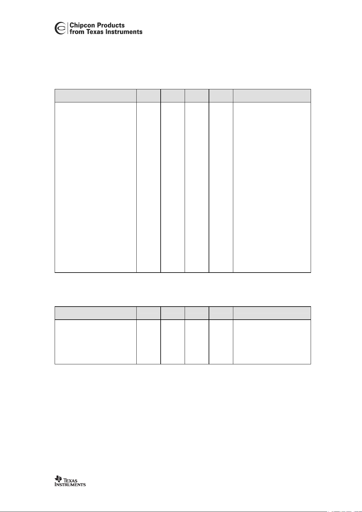
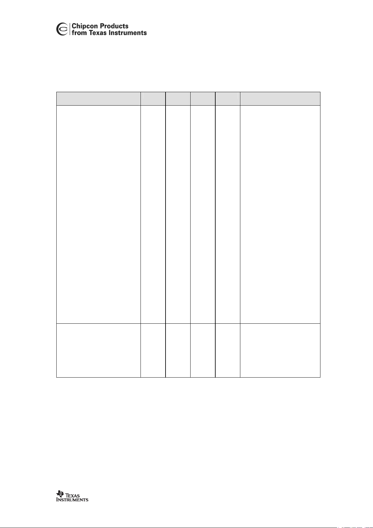
2. Absolute Maximum Ratings
Under no circumstances must the absolute maximum ratings given in Table 1 be violated.
Stress exceeding one or more of the limiting values may cause permanent damage to the
device.
Parameter Min. Max. Units Condition
Supply voltage, VDD -0.3 5.0 V
Voltage on any pin -0.3 VDD+0.3,
max 5.0
V
Input RF level 10 dBm
Storage temperature range -50 150
C
Un-programmed device
Storage temperature range -40 125
C
Programmed device, data
retention > 0.49 years at
125C
Lead temperature 260
C
T = 10 s
Table 1. Absolute Maximum Ratings
Caution! ESD sensitive device.
Precaution should be used when handling
the device in order to prevent permanent
damage.
3. Recommended Operating Conditions
Tc = -40 to 85C, VDD = 2.7 to 3.6 V if nothing else stated
Parameter
Min Typ Max Unit Condition
Supply voltage, DVDD, AVDD 2.7 3.3 3.6 V
Supply voltage during
normal operation
Supply voltage, DVDD, AVDD 2.7 3.6 V Supply voltage during
program/erase Flash
memory
Operating temperature, free-air -40 85
C
Main oscillator frequency
3 24 MHz
RTC oscillator frequency 32768 Hz
Table 2. Recommended Operating Conditions
Page 6
CC1010
SWRS047 Page 6 of 152
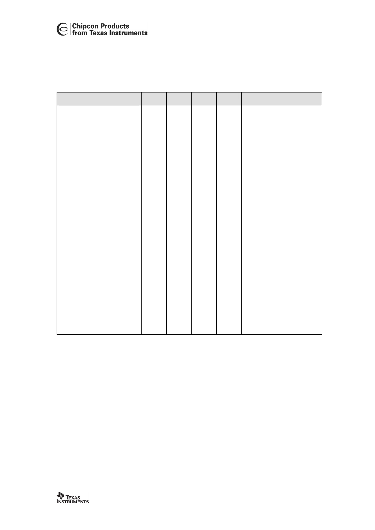
4. DC Characteristics
The DC Characteristics of
CC1010
are listed in Table 3 below.
Tc = 25C, VDD = 3.3 V if nothing else stated
Digital Inputs/Outputs
Min Max Unit Condition
Logic "0" input voltage
0 0.3*VDD V
Logic "1" input voltage
0.7*VDD VDD V
Logic "0" output voltage 0
0.4 V Output current -2.0 mA,
ports P0.3-P0.0, P1.7P1.0, P2.7-P2.4, P2.2P2.0
Logic "1" output voltage 2.5
VDD V Output current 2.0mA,
ports P0.3-P0.0, P1.7P1.0, P2.7-P2.4, P2.2P2.0
Logic "0" output voltage 0
0.4 V Output current -8.0 mA,
port P2.3
Logic "1" output voltage 2.5
VDD V Output current 8.0mA,
port P2.3
Logic "0" input current
NA -1
A
Input signal equals GND
Logic "1" input current
NA 1
A
Input signal equals VDD
Table 3. DC Characteristics
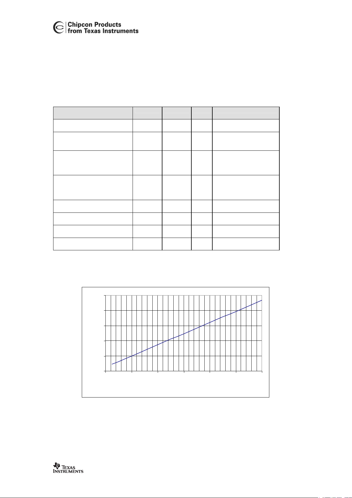
0
5
10
15
20
25
04812162024
Frequency [MHz]
Supply current [m A]
Figure 1. Typical CPU core supply current vs. clock frequency
Page 7
CC1010
SWRS047 Page 7 of 152
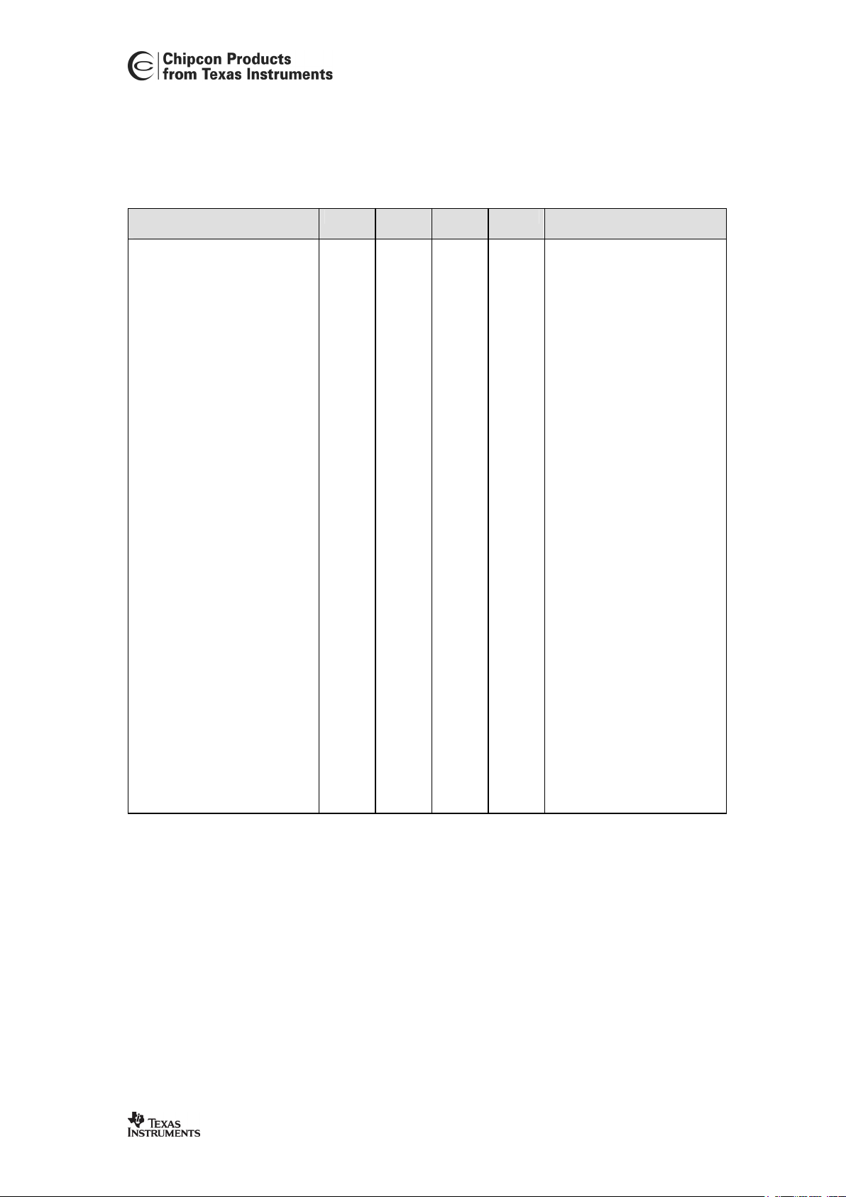
5. Electrical Specifications
Tc = 25C, VDD = 3.3 V if nothing else stated
All electrical specifications are measured on Chipcon’s CC1010EM reference design.
Parameter
Min. Typ. Max. Unit Condition
Power on reset (POR) voltage 2.7 2.9 3.1 V Tc = -40 to 85°C
Brown out voltage 2.7 2.9 3.1 V Tc = -40 to 85°C
RTC start-up time 160 ms
Current consumption MCU,
Active mode
14.8
1.3
mA
mA
14.7456 MHz, main oscillator
32 kHz, RTC oscillator
See page 33 for explanation
of modes. See Figure 1 page
6 for supply current vs. clock
frequency
Current consumption MCU, Idle
mode
12.8
29.4
mA
A
14.7456 MHz, main oscillator
32 kHz, RTC oscillator
Current consumption, Power
Down mode
0.2 1
A
Current consumption, Poweron reset circuit (when enabled)
34 uA
Current consumption Main
crystal oscillator
67 µA 14.7456 MHz crystal
Current consumption RF
Transceiver, Receive mode,
433/868 MHz
9.1/
11.9
mA Current for RF transceiver
alone
Current consumption RF
Transceiver, Transmit mode,
433/868 MHz
P=0.01 mW (-20 dBm)
P=0.3 mW (-5 dBm)
P=1 mW (0 dBm)
P=2.5 mW (4 dBm)
P=10 mW (10 dBm)
5.3/8.6
8.9/13.8
10.4/17
24.8/
23.5
26.6/NA
mA
mA
mA
mA
mA
The output power is delivered
to a single-ended 50 load,
see also page 123. Current is
for RF transceiver alone
32 kHz oscillator crystal load
capacitance
12 pF
Table 4. Electrical specifications
Page 8
CC1010
SWRS047 Page 8 of 152
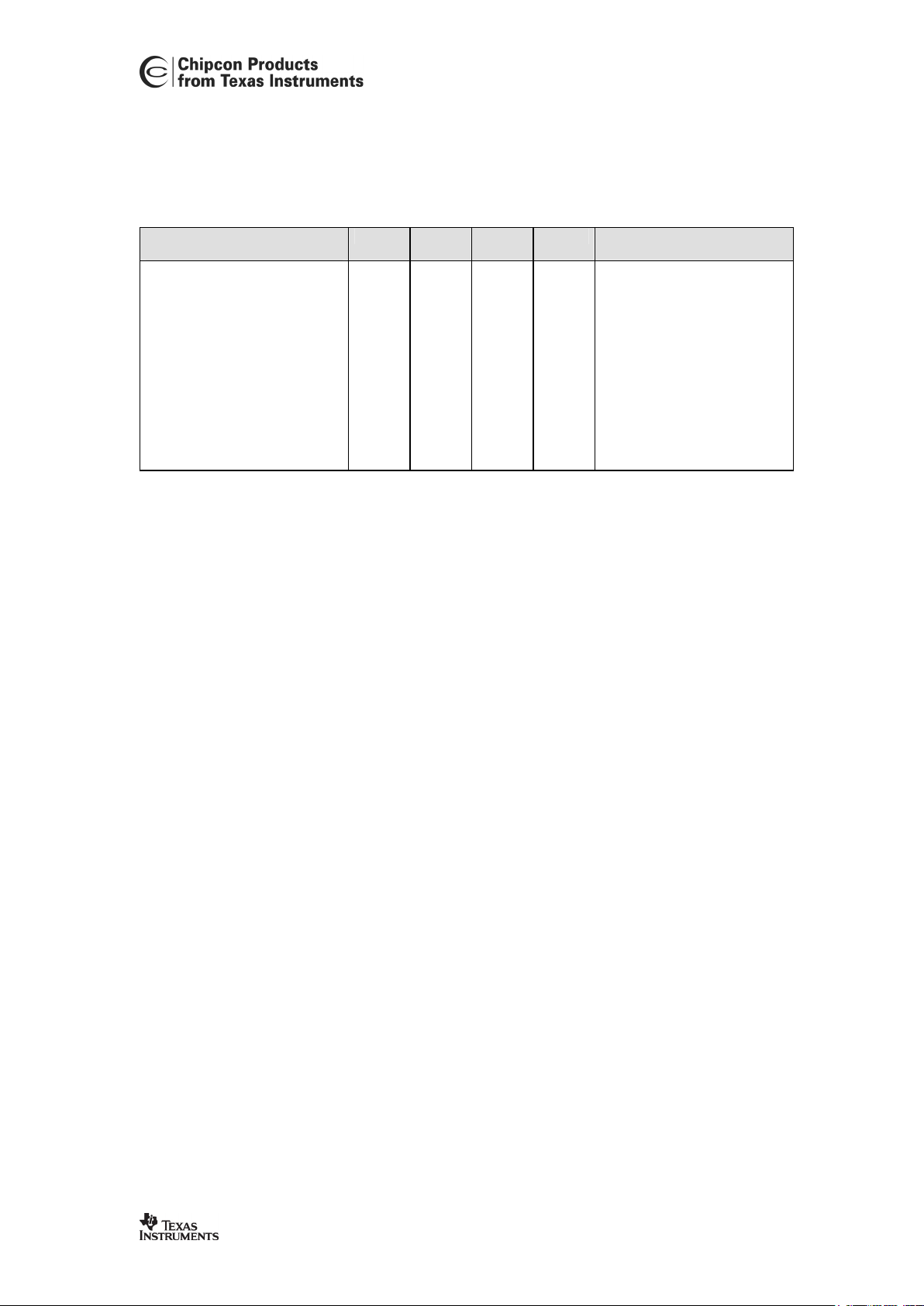
6. ADC
Parameter
Min. Typ. Max. Unit Condition
Number of bits 10 bits
Differential Nonlinearity (DNL) +/-0.2 LSB VDD is reference voltage
Integral Nonlinearity (INL)
+/-1.3 LSB VDD is reference voltage
Offset 3 LSB 7 Hz test tone
Total Harmonic Distortion
(THD)
59 dB 7 Hz test tone
SINAD 54
9
dB
bits
7 Hz test tone
Internal reference tolerance
± 10 %
Conversion time 44 µs When ADC is operated at 250
kHz
Clock frequency 32 250 250 kHz 250 kHz recommended for full
10-bit performance
External reference voltage 1.3 2.7 V External reference voltage
should never exceed 2.7 V. It
is recommended to use a
reference voltage close to 1.3
V to have the best possible
linearity.
Input voltage 0 Vref V
Table 5. ADC characteristics
7. RF section, general
Parameter
Min. Typ. Max. Unit Condition
RF Frequency Range 300
1000 MHz Programmable in steps of
< 250 Hz
Data rate
0.6 76.8 kBaud NRZ or Manchester encoding.
76.8 kBaud equals 76.8 kbps
using NRZ coding. See page
94
Table 6 General RF characteristics
Page 9
CC1010
SWRS047 Page 9 of 152
8. RF transmit section
Parameter
Min. Typ. Max. Unit Condition
Binary FSK frequency
separation
0 64 65 kHz The frequency corresponding
to the digital "0" is denoted f
0
,
while f
1
corresponds to a
digital "1".
The frequency separation is
f
1-f0
. The RF carrier
frequency, f
c
, is then given by
f
c
=(f0+f1)/2.
(The frequency deviation is
given by fd=+/-(f1-f0)/2 )
The frequency separation is
programmable in 250 Hz
steps. Separations up to 65
kHz are guaranteed at 1 MHz
reference frequency. Larger
separations can be achieved
at higher reference
frequencies
Output power
433 / 868 MHz
-20 0 10/4 dBm Delivered to single-ended 50
load.
The output power is
programmable, see page 123
RF output impedance
433 / 868 MHz
140/80
Transmit mode, optimum load
impedance. For matching
details see “Input/ output
matching” p.120
Harmonics
2
nd
harmonic, 433 / 868 MHz
3
rd
harmonic, 433 / 868 MHz
-7/-15
-27/-29
dBm
Conducted measur at
maximum output power. An
external LC filter should be
used to reduce harmonics
emission to comply with SRD
requirements. See p.128
Table 7. RF transmit characteristics
Page 10
CC1010
SWRS047 Page 10 of 152
9. RF receive section
Parameter
Min. Typ. Max. Unit Condition
Receiver Sensitivity,
433 / 868 MHz
-107/
-106
dBm 2.4 kBaud, Manchester coded
data, 64 kHz frequency
separation, BER = 10-3
See Table 33 and Table
34page 105 for typical
sensitivity figures at other
data rates.
System noise bandwidth 30 kHz 2.4 kBaud, Manchester coded
data
Cascaded noise figure
433/868 MHz
12/13 dB
Saturation (maximum input
level)
10 dBm 2.4 kBaud, Manchester coded
data, BER = 10
-3
-1 dBm 76.8 kBaud NRZ, BER = 10-3
Input IP3 -26 dBm From LNA to IF output
Blocking 40 dBc At +/- 1 MHz
LO leakage -57 dBm
Input impedance
90-j13
68-j24
36-j11
36-j13
Receive mode, series
equivalent
at 315 MHz
at 433 MHz
at 868 MHz
at 915 MHz
For matching details see
“Input/ output matching” p.
120.
Turn on time 11 128 Baud The demodulator settling
time, which is programmable,
determines the turn-on time.
See page 97 for details.
Table 8. RF receive characteristics
Page 11
CC1010
SWRS047 Page 11 of 152
10. IF section
Parameter
Min. Typ. Max. Unit Condition
Intermediate frequency (IF)
433/868 MHz
150/
130
10.7
kHz
MHz
Internal IF filter
External IF filter
IF bandwidth (noise bandwidth) 175 kHz
RSSI dynamic range
-105 -60 dBm
RSSI 3-dB bandwidth 260 kHz 868 MHz CW, -70 dBm
RSSI accuracy
6
dB See p. 126 for details
RSSI linearity
2
dB
Table 9 IF characteristics
Page 12
CC1010
SWRS047 Page 12 of 152
11. Frequency synthesizer section
Parameter
Min. Typ. Max. Unit Condition
Crystal Oscillator Frequency 3 24 MHz Crystal frequency can be 3-4,
6-8 or 9-24 MHz.
Recommended frequencies
are 3.6864, 7.3728, 11.0592,
14.7456, 18.4320 and
22.1184 MHz. See page 32
for details
Crystal frequency accuracy
requirement
50
25
ppm 433 MHz
868 MHz
The crystal frequency
accuracy and drift (ageing
and temperature
dependency) will determine
the frequency accuracy of the
transmitted signal.
Crystal operation
Parallel
C171 and C181 are loading
capacitors
Crystal load capacitance 12
12
12
12
20
16
16
12
30
30
16
16
pF
pF
pF
pF
3-4 MHz, 20 pF recommended
6-8 MHz, 16 pF recommended
9-16 MHz, 16 pF recommended
16-24 MHz, 12 pF recommended
Crystal oscillator start-up time 5
1.5
2
ms
ms
ms
3.6864 MHz, 16 pF load
7.3728 MHz, 16 pF load
16 MHz, 16 pF load
Output signal phase noise
-85 dBc/Hz At 100 kHz offset from carrier
PLL lock time (RX / TX turn
time)
200
s
PLL turn-on time 250
s
Table 10. Frequency synthesizer characteristics
Page 13
CC1010
SWRS047 Page 13 of 152
12. Pin Configuration
17
AGND
CC1010
1AVDD
2AVDD
3AGND
4RF_IN
5RF_OUT
6AVDD
7AGND
8AGND
9AGND
10L1
11L2
12AVDD
13CHP_OUT
14R_BIAS
15AVDD
16AGND
18
XOSC_Q119XOSC_Q2
20
XOSC32_Q2
21
XOSC32_Q1
22
AGND
23
DGND24DGND
25
POR_E
26
P1.0
27
(RXD1) P2.0
28
(TXD1) P2.1
29
(PWM3) P3.5
30
(PWM2) P3.4
31
(INT1) P3.3
32
48
47
46
45
44
43
42
41
40
39
38
37
36
35
34
33
64 63 62 61 60 59 58 57 56 55 54 53 52 51 50 49
DGND
P3.0 (RXD0)
P3.1 (TXD0)
P3.2 (INT0)
P2.5
P2.4
DVDD
P2.3
DGND
DVDD
P2.2
P1.4
P1.3
P1.2
P1.1
P0.1 (MOSI)
P0.0 (SCK)
AGND
AD2 (RSSI/IF)
AD1
AD0
DVDD
RESET
PROG
P2.7
P2.6
P1.7
P1.6
P1.5
P0.3
P0.2 (MISO)
DVDD
DGND
(Top view)
Pin
#
Pin name Alternate
function
Pin type Description
1 AVDD - Power (A) Power supply ADC
2 AVDD - Power (A) Power supply Mixer and IF
3 AGND - Power (A) Ground connection Mixer and IF
4 RF_IN - RF input RF signal input from antenna (external AC-
coupling)
5 RF_OUT - RF output RF signal output to antenna
6 AVDD - Power (A) Power supply LNA and PA
7 AGND - Power (A) Ground connection LNA and PA
8 AGND - Power (A) Ground connection PA
9 AGND - Power (A) Ground connection VCO and prescaler
10 L1 - Analog Connection #1 for external VCO tank
inductor
11 L2 - Analog Connection #2 for external VCO tank
inductor
12 AVDD - Power (A) Power supply VCO and prescaler
Page 14

CC1010
SWRS047 Page 14 of 152
Pin
#
Pin name Alternate
function
Pin type Description
13 CHP_OUT - Analog output Charge pump current output when external
loop filter is used
14 R_BIAS - Analog Connection for external precision bias
resistor (82 k, 1%)
15 AVDD - Power (A) Power supply misc. analog modules
16 AGND - Power (A) Ground connection misc. analog modules
17 AGND - Power (A) Analog ground connection
18 XOSC_Q1 - Analog input 3-24 MHz crystal, pin 1 or external clock
input
19 XOSC_Q2 - Analog output 3-24 MHz crystal, pin 2
20 XOSC32_Q2 - Analog output 32 kHz crystal pin2
21 XOSC32_Q1 - Analog input 32 kHz crystal pin1 or external clock input
22 AGND - Power (A) Analog ground connection
23 DGND - Power (D) Digital ground connection
24 DGND - Power (D) Digital ground connection
25 POR_E - Digital input Power-on reset enable.
0: Disable internal power-on reset module
1: Enable internal power-on reset module
26 P1.0 - Digital high-Z I/O 8051 port 1, bit 0
27 P2.0 RXD1 (I) Digital high-Z I/O 8051 port 2, bit 0 or RX of serial port 1
28 P2.1 TXD1 (O) Digital high-Z I/O 8051 port 2, bit 1 or TX of serial port 1
29 P3.5 PWM3 (O)
T1 (I)
Digital high-Z I/O 8051 port 3, bit 5 or pulse width modulator
3's output or Timer / Counter 1 external input
30 P3.4 PWM2 (O)
T0 (I)
Digital high-Z I/O 8051 port 3, bit 4 or pulse width modulator
2's output or Timer / Counter 0 external input
31 P3.3
INT1
(I)
Digital high-Z I/O 8051 port 3, bit 3 or interrupt 1 input
configurable as level or edge sensitive
32 DGND - Power (D) Ground connection digital part
33 P0.0 SCK (O)
SCK (I)
Digital high-Z I/O 8051 port 0, bit 0 or SPI master interface
serial clock output or Flash programming
SPI slave clock input.
34 P0.1 MO (O)
SI (I)
Digital high-Z I/O 8051 port 0, bit 1 or SPI interface master
output or Flash programming SPI slave
serial data input
35 P1.1 - Digital high-Z I/O 8051 port 1, bit 1
36 P1.2 - Digital high-Z I/O 8051 port 1, bit 2
37 P1.3 - Digital high-Z I/O 8051 port 1, bit 3
38 P1.4 - Digital high-Z I/O 8051 port 1, bit 4
39 P2.2 - Digital high-Z I/O
(Schmitt trigger
input)
8051 port 2, bit 2
40 DVDD - Power (D) Digital power supply
41 DGND - Power (D) Ground connection digital part
42 P2.3 - Digital high-Z I/O (8
mA)
8051 port 2, bit 3
43 DVDD - Power (D) Digital power supply
44 P2.4 - Digital high-Z I/O 8051 port 2, bit 4
45 P2.5 - Digital high-Z I/O 8051 port 2, bit 5
46 P3.2
INT0
(I)
Digital high-Z I/O 8051 port 3, bit 2 or interrupt 0 input
configurable as level or edge sensitive
47 P3.1 TXD0 (O) Digital high-Z I/O 8051 port 3, bit 1 or TX of serial port 0
48 P3.0 RXD0 (I) Digital high-Z I/O 8051 port 3, bit 0 or RX of serial port 1
49 DGND - Power (D) Digital ground connection
50 DVDD - Power (D) Digital power supply
Page 15
CC1010
SWRS047 Page 15 of 152
Pin
#
Pin name Alternate
function
Pin type Description
51 P0.2 MI (I)
SO (O)
Digital high-Z I/O 8051 port 0, bit 2 or SPI interface master
input or Flash programming SPI slave serial
data output
52 P0.3 - Digital high-Z I/O 8051 port 0, bit 3
53 P1.5 - Digital high-Z I/O 8051 port 1, bit 5
54 P1.6 - Digital high-Z I/O 8051 port 1, bit 6
55 P1.7 - Digital high-Z I/O 8051 port 1, bit 7
56 P2.6 - Digital high-Z I/O 8051 port 2, bit 6
57 P2.7 - Digital high-Z I/O 8051 port 2, bit 7
58
PROG
- Digital input Flash program enable pad, active low
59
RESET
- Digital input (pull-up) System reset pin, active low
60 DVDD - Power (D) Digital power supply
61 AD0 - Analog input ADC input channel 0
62 AD1 - Analog input ADC input channel 1
63 AD2 RSSI (O),
IF (O)
Analog input/output ADC input channel 2, RSSI (Receiver signal
strength indicator) output, or IF output when
using external demodulator
64 AGND - Power (A) Analog ground connection ADC
A = Analog, D = Digital, I = input, O= Output
13. Pin description
AVDD, DVDD
Supply voltages for analog and digital
modules respectively. All supply pins
should be decoupled by capacitors. In
particular, the digital and analog supply
domains should be properly decoupled
from each other (a ferrite bead can be
used to prevent high-frequency noise from
coupling from one supply domain to
another). The placement and size of
decoupling capacitors and supply filtering
are critical with respect to LO leakage and
sensitivity. Chipcon’s reference layout
designs should be used (available from
Chipcon’s website). See also page 133 for
layout recommendations.
AGND, DGND
Ground for analog and digital modules
respectively. Normally one common
ground plane is recommended. If two
separate analog and digital grounds are
used they should be interconnected in one
place, and one place only.
RFIN
This is the RF input, internally connected
to the low noise amplifier (LNA). The
signal source (antenna) should be
matched to the input impedance. A DC
ground is needed for LNA biasing.
RFOUT
This is the RF output, internally connected
to the power amplifier (PA). The external
load (antenna) should be matched to the
output impedance (optimum load
impedance). This pin must be DC coupled
to AVDD for PA biasing (open drain
output).
L1, L2
Connection to internal voltage controlled
oscillator (VCO). An inductor should be
connected between these pins. The
inductor value will determine the VCO
tuning range. The inductor should be place
very close to the pins in order to minimize
paracitic inductance.
CHP_OUT
Charge Pump output. If the RF transceiver
is configured for external loop filter this is
the current output from the charge pump.
Normally the internal loop filter should be
used and this pin should be left open (not
connected).
Page 16

CC1010
SWRS047 Page 16 of 152
RBIAS
Current output from internal band gap cell
bias generator. A precision resistor (82
k, 1%) should be connected between
this pin and ground to set the correct bias
current level.
XOSC_Q1, XOSC_Q2
These are the main oscillator connection
pins. An external crystal should be
connected between these pins, and load
capacitors should be connected between
each pin and ground. If an external
oscillator is used, the clock signal should
be connected to the XOSC_Q1 pin, and
XOSC_Q2 should be left open (not
connected).
XOSC32_Q1, XOSC32_Q2
These are the real time clock (RTC)
oscillator connection pins. An external
crystal should be connected between
these pins, and load capacitors should be
connected between each pin and ground.
If an external oscillator is used, the clock
signal should be connected to the
XOSC32_Q1 pin, and XOSC32_Q2
should be left open (not connected).
POR_E
Enable signal for the on-chip power-on
reset module. The power-on reset is
enabled when POR_E is connected to
DVDD and disabled when connected to
DGND.
PROG
Active low Flash programming enable pin.
When this signal is active (driven to DGND)
a Flash programmer can be connected to
the SPI interface. Under normal operation
it must be driven to DVDD.
RESET
Active low asynchronous system reset. It
has an internal pull-up resistor and can be
left unconnected during normal operation.
AD0, AD1
Analog inputs to A/D converter channels 0
and 1 respectively. When not used these
pins can be left open (not connected).
AD2 (RSSI/IF)
Analog input to A/D converter channel 2.
This pin can also be configured to be RSSI
output or IF output. The pin is configured
by the FREND register. When not used this
pin can be left open (not connected).
PORT 0
Port 0 is a 4-bit (P0.3-P0.0) bi-directional
CMOS I/O port with 2 mA drivers. A
direction register (P0DIR) controls whether
each pin is an output or input and the
register P0 is used to read the input or
control the logical value of the output.
Pins P0.0 - P0.2 can be configured to
become a master SPI interface in register
SPCR and will then override P0(2:0),
P0DIR(2) and P0DIR(1).
Used as SPI interface, P0.0 is SCK,
P0.1 is MOSI, and P0.2 is MISO.
PORT 1
Port 1 is an 8-bit (P1.7-P1.0) bidirectional CMOS I/O port with 2 mA
drivers. A direction register (P1DIR)
controls whether each pin is an output or
input and the register P1 is used to read
the input or control the logical value of the
output.
PORT 2
Port 2 is an 8-bit (P2.7-P2.0) bidirectional CMOS I/O port with 2 mA
drivers, except for P2.3 that has an 8 mA
output buffer. A direction register (P2DIR)
controls whether each pin is an output or
input and the register P2 is used to read
the input or control the logical value of the
output.
Pins P2.0 and P2.1 can be configured to
become the RXD1 and TXD1 pin,
respectively, of UART 1.
Pin P2.2 has a Schmitt-trigger input
stage. Note that while this pin does have
hysteresis, it will draw a large input current
(~0.5 mA) if the input voltage is close to
VDD/2.
PORT 3
Port 3 is a 6-bit (P3.5-P3.0) bi-directional
CMOS I/O port with 2 mA drivers. A
direction register (P3DIR) controls whether
each pin is an output or input. The register
P3 is used to read the input or control the
logical value of the output.
Page 17

CC1010
SWRS047 Page 17 of 152
Pins P3.0 and P3.1 can be configured to
become the RXD0 and TXD0 pin,
respectively, of UART 0.
Pins P3.2 and P3.3 are connected to the
external interrupt inputs
INT0 and
INT1
,
respectively, and can cause interrupts if
the corresponding interrupt enable flags
are set in register
IE. The interrupts inputs
can be configured to be either levelsensitive or edge-sensitive.
Pins
P3.4 and P3.5 can be configured to
become the pulse width modulator (PWM)
outputs of Timer/PWM 2 and Timer/PWM
3, respectively. When pulse width
modulation is enabled the corresponding
bits in
P3DIR and P3 are overridden.
Page 18
CC1010
SWRS047 Page 18 of 152
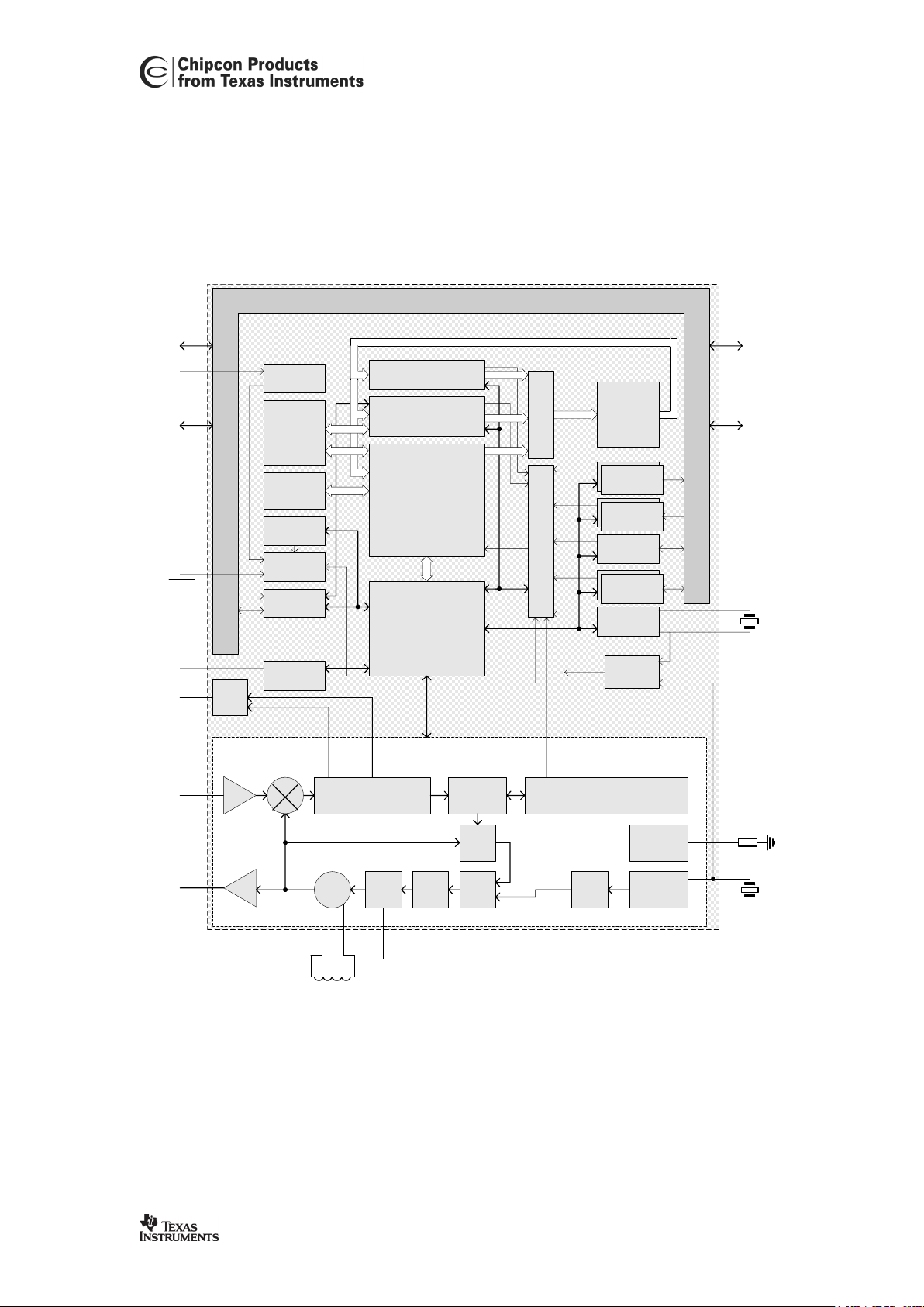
14. Block Diagram
The
CC1010
Block Diagram is shown in Figure 2 below.
Figure 2. CC1010 Block Diagram
32 kB
FLASH
128 byte
SRAM
Special Function
Registers
(SFRs)
Interrupt
Controller
Realtime
Clock
Watchdog
Timer
SPI
Timers/
Counters
Timers/
PWMs
UARTs
UARTs
General
purpose I/O
CODEC, Bit synchronizer,
Serializer/Deserializer
IF stage MODEM
RF Transceiver
8051 core
FLASH
Programming DMA
DES Module
2048 byte
SRAM
RAM Arbiter
Reset
Generation
3-24 MHz crystal
32 kHz crystal
Clock
Multiplexer
System
clock
Port 0
Port 1
Port 2
Port 3
RESET
PROG
RF_IN
ADC
Programmable I/O (General purpose or alternate function)
Power-on
reset
POR_E
Main Crystal
Oscillator
:R
:N.n
RF_OUT
LPF CHP PD
MUX
RSSIIF
Bias
Bias resistor
VCO inductor
VCO
CHP_OUT
AD2
(RSSI/IF)
AD0
AD1
PA
LNA
MIXER
L1 L2
Page 19

CC1010
SWRS047 Page 19 of 152
15. 8051 Core
15.1 General description
The
CC1010
microcontroller core is based
on the industry-standard 8051
architecture. The MCU core is 8-bit, with
program and data memory located in
separate memory spaces (Harvard
architecture). The internal registers are
organised as four banks of 8 registers
each. The instruction set supports direct,
indirect and register addressing modes.
Program memory can be addressed using
indexed addressing. The core registers
are comprised of an accumulator, a stack
pointer and dual data pointer registers in
addition to the general registers.
Data memory is split into internal and
external RAM. The name "external RAM"
is in fact misleading since in the case of
the
CC1010
all the RAM is internal to the
chip. The difference between external and
internal is that external RAM can only be
accessed by a few instructions. Therefore,
frequently-accessed variables as well as
the stack should be kept in internal RAM.
The various peripherals are controlled
through Special Function Registers
(SFRs) located in the internal RAM space.
The 8051 core is instruction set
compatible with the industry standard
8051. It also has one additional instruction,
TRAP, to enable advanced in-circuit-
debugging features. This is described on
page 44.
The instruction cycle time is 4 clock
cycles, which typically gives a 2.5X
average reduction in instruction execution
time over the original Intel 8051.
Peripheral units, including general purpose
I/O, 2 standard 8051 timers, 2 extra timers
with PWM functionality, a watchdog timer,
a real-time clock, an SPI master interface,
hardware DES encryption, a true random
bit generator and ADC are all described
from page 47 and out. Dual data pointers
are available for faster data transfer.
15.2 Reset
CC1010
must be reset at start-up. There
are several sources for reset in
CC1010
:
External reset pin, RESET
. Applying
a low signal to this pin at any time will
reset almost all registers in
CC1010
.
Exceptions can be found in Table 41
on page 144. The input is
asynchronous and is synchronised
internally, so that the reset can be
released independent of the timing of
the active clock signal. If the main
crystal oscillator is inactive, the reset
input should be held long enough for
the oscillator to start up and stabilize.
See Electrical Specifications page 7
for oscillator start-up timing.
Power On Reset (POR). The internal
POR module can generate reset upon
power-up. Special requirements for
power consumption or power supply
voltage may require an external POR
module, as described in the Power On
Reset (Brown-Out Detection) section
at page 62.
Brown-out detection reset. The POR
will also detect low supply voltage and
generate a reset.
Watchdog timer reset. The watchdog
timer can generate a reset, as
described in the section on page 63.
ADC reset. The ADC module can be
programmed to generate a reset
signal if its inputs exceed a
programmed threshold. See the ADC
section on page 79 for details.
The POR and ADC reset signals will be
held for 1024 clock periods after the signal
is released. This will ensure a safe clock
start-up if the crystal oscillator is currently
not running.
Page 20

CC1010
SWRS047 Page 20 of 152
15.3 Memory Map
The
CC1010
memory map is shown in
Figure 3.
CC1010
has 2 blocks of RAM on chip. This
includes the 128 bytes Internal RAM and
the 2048 bytes External RAM. (The 2048byte RAM will be referred to as External
RAM, although it is on-chip. Direct access
to off-chip RAM is not implemented.)
Access to the internal RAM is performed
using the MOV instruction. MOV A, @Ri,
MOV @Ri, A and MOV @Ri, #data use
indirect addressing. MOV A, direct,
MOV Rn, direct, MOV direct, A,
MOV direct, Rn, MOV direct,
direct and MOV direct, #data use
direct addressing. MOV @Ri, direct
uses indirect and direct addressing.
All direct addressing instructions can also
be used to access the SFRs.
CC1010
also
implements the option to access SFRs
indirectly, as described in the In Circuit
Debugging section on page 44.
CC1010
has
dual data pointers to external RAM,
provided in the 16 bit registers
DPTR0 and
DPTR1 (SFRs DPH0, DPL0, DPH1 and
DPL1). If a high-level language compilator
is used, it should be set up to make use of
both pointers for better performance. The
data pointer is selected through
DPS.SEL.
Access to the external RAM is performed
using the MOVX instruction and indirect
addressing using either the 16 bit data
pointers or the 8 bit registers R0 or R1
together with
MPAGE. MOVX A, @DPTR
and MOVX @DPTR, A
moves data to (from) the accumulator,
from (to) the address pointed to by the
currently selected data pointer.
The instructions MOVX A, @Ri and MOVX
@Ri, A moves data to (from) the
accumulator, from (to) the address given
by the memory page address register
MPAGE and the register Ri (R0 or R1).
MPAGE gives the 8 most significant
address bits, while the register Ri gives
the 8 least significant bits. In many 8051
implementations, this type of external
RAM access is performed using
P2 to give
the most significant address bits. Existing
software may therefore have to be
adapted to make use of
MPAGE instead of
P2.
The program memory can be read using
the MOVC A, @A+DPTR and MOVC A,
@A+PC instructions, which moves a byte
from the program memory address given
by A+DPTR or A+PC respectively. The
program memory can not be written using
MOV commands, but uses the method
described in the 8051 Flash Programming
section on page 42.
CC1010
also provides a possibility to stretch
the access cycle to external RAM, through
CKCON.MD(2:0) (see page 55). The
default value for
CKCON.MD is "001". It is
recommended to set
CKCON.MD to "000"
for faster RAM access.
Page 21
CC1010
SWRS047 Page 21 of 152
Internal RAM
Accessible
through Direct
and Indirect
Addressing
0x00
0x7F
Special Function
Registers (SFR),
accessible
through Direct
Addressing
0xFF
Accesible
through indirect
addressing
0x7FF
Internal RAM / SFR
External RAM
0x00
Flash Program
Memory
0x00
Accesible
through indirect
addressing
0x7FFF
Figure 3. Memory Map
DPL0 (0x82) - Data Pointer 0, low byte
Bit Name R/W Reset value Description
7:0
DPL0(7:0)
R/W 0x00 Data Pointer 0, low byte
DPH0 (0x83) - Data Pointer 0, high byte
Bit Name R/W Reset value Description
0
DPH0(7:0)
R/W 0x00 Data Pointer 0, high byte
DPL1 (0x84) - Data Pointer 1, low byte
Bit Name R/W Reset value Description
7:0
DPL1(7:0)
R/W 0x00 Data Pointer 1, low byte
DPH1 (0x85) - Data Pointer 1, high byte
Bit Name R/W Reset value Description
7:0
DPH1(7:0)
R/W 0x00 Data Pointer 1, high byte
Page 22
CC1010
SWRS047 Page 22 of 152
DPS (0x86) - Data Pointer Select
Bit Name R/W Reset value Description
7:1
-
R0 0x00 Reserved, read as 0
0
SEL
R/W 0x00 Data Pointer Select for external RAM access
0 :
DPH0 and DPL0 are used
1 :
DPH1 and DPL1 are used
MPAGE (0x92) - Memory Page Select Register
Bit Name R/W Reset value Description
7:0
MPAGE(7:0)
R/W 0x00 Memory Page
A total of 119 Special Function Registers
(SFRs) are accessible from the
microcontroller core. The names and
addresses of all SFRs are listed in Table
11. All standard 8051 registers are
available, in addition to SFRs which are
CC1010
specific, controlling modules such
as the RF Transceiver, DES encryption,
ADC and Real-Time Clock.
All SFRs will be described in the following
sections. A more detailed overview is
provided in Table 41 on page 144, which
also includes all reset values. SFRs with
addresses ending with 0 or 8 (leftmost
column of Table 11) are bit adressable.
0/8 1/9 2/A 3/B 4/C 5/D 6/E 7/F
0xF8
EIP TEST0 TEST1 TEST2 TEST3 TEST4 TEST5 TEST6
0xF0
B FSHAPE7 FSHAPE6 FSHAPE5 FSHAPE4 FSHAPE3 FSHAPE2 FSHAPE1
0xE8
EIE FSDELAY FSEP0 FSEP1 FSCTRL RTCON FREND TESTMUX
0xE0
ACC CURRENT PA_POW PLL LOCK CAL PRESCALER RESERVED
0xD8
EICON MODEM2 MODEM1 MODEM0 MATCH FLTIM - -
0xD0
PSW X32CON WDT PDET BSYNC - - -
0xC8
RFMAIN RFBUF FREQ_0A FREQ_1A FREQ_2A FREQ_0B FREQ_1B FREQ_2B
0xC0
SCON1 SBUF1 RFCON CRPCON CRPKEY CRPDAT CRPCNT RANCON
0xB8
IP RDATA RADRL RADRH CRPINI4 CRPINI5 CRPINI6 CRPINI7
0xB0
P3 - - - CRPINI0 CRPINI1 CRPINI2 CRPINI3
0xA8
IE TCON2 T2PRE T3PRE T2 T3 FLADR FLCON
0xA0
P2 SPCR SPDR SPSR P0DIR P1DIR P2DIR P3DIR
0x98
SCON0 SBUF0 - - - - - CHVER
0x90
P1 EXIF MPAGE ADCON ADDATL ADDATH ADCON2 ADTRH
0x88
TCON TMOD TL0 TL1 TH0 TH1 CKCON -
0x80
P0 SP DPL0 DPH0 DPL1 DPH1 DPS PCON
Table 11
CC1010
SFR Overview
Page 23

CC1010
SWRS047 Page 23 of 152
15.4 CPU Registers
CC1010
provides 4 register banks of 8
registers each. These register banks are
mapped in the the internal data memory
(see the Memory section on page 33) at
addresses 0x00 - 0x07, 0x08 - 0x0F, 0x10
- 0x17 and 0x18 - 0x1F. Each register
bank contains the 8 8-bit registers R0
through R7. The different register banks
are selected through the Program Status
Word
PSW.RS(1:0) as shown below.
PSW also contains carry, overflow and
parity flags that reflect the current CPU
state.
In addition, the CPU uses the accumulator
register
A (accessed via the SFR space as
ACC), B (for multiplication and division) and
the stack pointer
SP. These registers are
shown below. Note that the hardware
stack pointer
SP is increased when
pushing and decreased when popping
data, unlike many other microcontroller
architectures.
PSW (0xD0) - Program Status Word
Bit Name R/W Reset value Description
7
CY
R/W 0 Carry Flag, set to 1 when the last arithmetic
operation resulted in a carry (during addition) or
borrow (during subtraction), otherwise cleared to
0 by all arithmetic operations.
CY is also used for
rotation instructions.
6
AC
R/W 0 Auxiliary carry flag. Set to 1 when the last
arithmetic operation resulted in a carry into
(during addition) or borrow from (during
subtraction) the high order nibble, otherwise
cleared to 0 by all arithmetic operations.
5
F0
R/W 0 Flag 0 (Available to the user for general purpose)
4
RS1
R/W 0
3
RS0
R/W 0
Register bank select.
RS1 RS0 Working register bank and address
0 0 Bank0 0x00-0x07
0 1 Bank1 0x08-0x0F
1 0 Bank2 0x10-0x17
1 1 Bank3 0x18-0x1F
2
OV
R/W 0 Overflow flag. Set to 1 when the last arithmetic
operation resulted in a carry (addition), borrow
(subtraction), or overflow (multiply or divide).
Otherwise, the bit cleared to 0 by all arithmetic
operations.
1
F1
R/W 0 Flag 1 (Available to the user for general purpose)
0
P
R/W 0 Parity flag. Set to 1 when the modulo-2 sum of
the 8 bits in the accumulator is 1 (odd parity),
cleared to 0 on even parity.
ACC (0xE0) - Accumulator Register
Bit Name R/W Reset value Description
7:0
ACC(7:0)
R/W 0x00 Accumulator
B (0xF0) - B Register
Bit Name R/W Reset value Description
7:0
B(7:0)
R/W 0x00
B is used for multiplication and division
Page 24
CC1010
SWRS047 Page 24 of 152
SP (0x81) - Stack Pointer
Bit Name R/W Reset value Description
7:0
SP(7:0)
R/W 0x07 Stack Pointer, used for pushing and poping data
to and from the stack. Note that the reset value
for
SP is 0x07
15.5 Instruction Set Summary
The 8051 instruction set is summarised in
Table 12 below. All mnemonics are
Copyright Intel Corporation 1980.
One non-standard 8051 instruction, TRAP,
with opcode 0xA5 is included to enable
setting of breakpoints. This instruction is
described in the In Circuit Debugging
section at page 44. Symbols used in the
table are:
A - Accumulator
AB - Register pair A and B
B - Multiplication register
C - Carry flag
DPTR - Data pointer
Rn - Register R0 - R7
PC - Program counter
direct - 8-bit data address (Internal
RAM 0x00 - 0x7F, SFRs 0x80-0xFF)
@Ri - Internal register pointed to by R0
or R1 (except MOVX)
rel - Two's complement offset byte
used by SJMP and conditional jumps
bit - Direct bit address
#data - 8-bit constant
#data 16 - 16-bit constant
addr 16 - 16-bit destination address
addr 11 - 11-bit destination address,
used by ACALL and AJMP. The branch
will be within the same 2 kB block of
program memory of the first byte of
the following instruction.
The ‘Bytes’ column shows the number of
bytes of Flash memory used. Further, the
number of instruction cycles is shown.
Each instruction cycle requires four clock
cycles. The 4 rightmost columns shows
which flags in the program status word
PSW (see page 23) are affected by the
instructions.
Mnemonic Description
Bytes
Instr. Cycles
Hex Opcode
CY
AC
OV
P
Arithmetic
ADD A, Rn
Add register to A 1 1 28-2F x x x x
ADD A, direct
Add direct byte to A 2 2 25 x x x x
ADD A, @Ri
Add data memory to A 1 1 26-27 x x x x
ADD A, #data
Add immediate to A 2 2 24 x x x x
ADDC A, Rn
Add register to A with carry 1 1 38-3F x x x x
ADDC A, direct
Add direct byte to A with carry 2 2 35 x x x x
ADDC A, @Ri
Add data memory to A with carry 1 1 36-37 x x x x
ADDC A, #data
Add immediate to A with carry 2 2 34 x x x x
SUBB A, Rn
Subtract register from A with
borrow
1 1 98-9F x x x x
SUBB A, direct
Subtract direct byte from A with
borrow
2 2 95 x x x x
Page 25

CC1010
SWRS047 Page 25 of 152
Mnemonic Description
Bytes
Instr. Cycles
Hex Opcode
CY
AC
OV
P
SUBB A, @Ri
Subtract data memory from A with
borrow
1 1 96-97 x x x x
SUBB A, #data
Subtract immediate from A with
borrow
2 2 94 x x x x
INC A
Increment A 1 1 04 x
INC Rn
Increment register 1 1 08-0F
INC direct
Increment direct byte 2 2 05
INC @Ri
Increment data memory 1 1 06-07
DEC A
Decrement A 1 1 14 x
DEC Rn
Decrement register 1 1 18-1F
DEC direct
Decrement direct byte 2 2 15
DEC @Ri
Decrement data memory 1 1 16-17
INC DPTR
Increment data pointer 1 3 A3
MUL AB
Multiply A by B 1 5 A4 x x x
DIV AB
Divide A by B 1 5 84 x x x
DA A
Decimal adjust A 1 1 D4 x x
Logical
ANL A, Rn
AND register to A 1 1 58-5F x
ANL A, direct
AND direct byte to A 2 2 55 x
ANL A, @Ri
AND data memory to A 1 1 56-57 x
ANL A, #data
AND immediate to A 2 2 54 x
ANL direct, A
AND A to direct byte 2 2 52
ANL direct, #data
AND immediate data to direct byte 3 3 53
ORL A, Rn
OR register to A 1 1 48-4F x
ORL A, direct
OR direct byte to A 2 2 45 x
ORL A, @Ri
OR data memory to A 1 1 46-47 x
ORL A, #data
OR immediate to A 2 2 44 x
ORL direct, A
OR A to direct byte 2 2 42
ORL direct, #data
OR immediate data to direct byte 3 3 43
XRL A, Rn
Exclusive-OR register to A 1 1 68-6F x
XRL A, direct
Exclusive-OR direct byte to A 2 2 65 x
XRL A, @Ri
Exclusive-OR data memory to A 1 1 66-67 x
XRL A, #data
Exclusive-OR immediate to A 2 2 64 x
XRL direct, A
Exclusive-OR A to direct byte 2 2 62
XRL direct, #data
Exclusive-OR immediate to direct
byte
3 3 63
CLR A
Clear A 1 1 E4 x
CPL A
Complement A 1 1 F4 x
SWAP A
Swap nibbles of A 1 1 C4
RL A
Rotate A left 1 1 23
RLC A
Rotate A left through carry 1 1 33 x x
RR A
Rotate A right 1 1 03
RRC A
Rotate A right through carry 1 1 13 x x
Data Transfer
MOV A, Rn
Move register to A 1 1 E8-
EF
x
MOV A, direct
Move direct byte to A 2 2 E5 x
Page 26

CC1010
SWRS047 Page 26 of 152
Mnemonic Description
Bytes
Instr. Cycles
Hex Opcode
CY
AC
OV
P
MOV A, @Ri
Move data memory to A 1 1 E6-
E7
x
MOV A, #data
Move immediate to A 2 2 74 x
MOV Rn, A
Move A to register 1 1 F8-FF
MOV Rn, direct
Move direct byte to register 2 2 A8-
AF
MOV Rn, #data
Move immediate to register 2 2 78-7F
MOV direct, A
Move A to direct byte 2 2 F5
MOV direct, Rn
Move register to direct byte 2 2 88-8F
MOV direct,
direct
Move direct byte to direct byte 3 3 85
MOV direct, @Ri
Move data memory to direct byte 2 2 86-87
MOV direct, #data
Move immediate to direct byte 3 3 75
MOV @Ri, A
MOV A to data memory 1 1 F6-F7
MOV @Ri, direct
Move direct byte to data memory 2 2 A6-
A7
MOV @Ri, #data
Move immediate to data memory 2 2 76-77
MOV DPTR, #data
Move immediate to data pointer 3 3 90
MOVC A, @A+DPTR
Move code byte relative DPTR to A 1 3 93 x
MOVC A, @A+PC
Move code byte relative PC to A 1 3 83 x
MOVX A, @Ri
Move external data (A8) to A 1 2-9 E2-
E3
x
MOVX A, @DPTR
Move external data (A16) to A 1 2-9 E0 x
MOVX @Ri, A
Move A to external data (A8) 1 2-9 F2-F3
MOVX @DPTR, A
Move A to external data (A16) 1 2-9 F0
PUSH direct
Push direct byte onto stack 2 2 C0
POP direct
Pop direct byte from stack 2 2 D0
XCH A, Rn
Exchange A and register 1 1 C8-
CF
x
XCH A, direct
Exchange A and direct byte 2 2 C5 x
XCH A, @Ri
Exchange A and data memory 1 1 C6-
C7
x
XCHD A, @Ri
Exchange A and data memory
nibble
1 1 D6-
D7
x
Boolean
CLR C
Clear carry 1 1 C3 x
CLR bit
Clear direct bit 2 2 C2
SETB C
Set carry 1 1 D3 x
SETB bit
Set direct bit 2 2 D2
CPL C
Complement carry 1 1 B3 x
CPL bit
Complement direct bit 2 2 B2
ANL C, bit
AND direct bit to carry 2 2 82 x
ANL C, /bit
AND direct bit inverse to carry 2 2 B0 x
ORL C, bit
OR direct bit to carry 2 2 72 x
ORL C, /bit
OR direct bit inverse to carry 2 2 A0 x
MOV C, bit
Move direct bit to carry 2 2 A2 x
MOV bit, C
Move carry to direct bit 2 2 92
Page 27

CC1010
SWRS047 Page 27 of 152
Mnemonic Description
Bytes
Instr. Cycles
Hex Opcode
CY
AC
OV
P
Branching
ACALL addr 11
Absolute call to subroutine 2 3 11-F1
LCALL addr 16
Long call to subroutine 3 4 12
RET
Return from subroutine 1 4 22
RETI
Return from interrupt 1 4 32
AJMP addr 11
Absolute jump unconditional 2 3 01-E1
LJMP addr 16
Long jump unconditional 3 4 02
SJMP rel
Short jump (relative address) 2 3 80
JC rel
Jump on carry = 1 2 3 40
JNC rel
Jump on carry = 0 2 3 50
JB bit, rel
Jump on direct bit = 1 3 4 20
JNB bit, rel
Jump on direct bit = 0 3 4 30
JBC bit, rel
Jump on direct bit = 1 and clear 3 4 10
JMP @A+DPTR
Jump indirect relative DPTR 1 3 73
JZ rel
Jump on accumulator = 0 2 3 60
JNZ rel
Jump on accumulator /= 0 2 3 70
CJNE A, direct,
rel
Compare A and direct, jump
relative if not equal
3 4 B5 x
CJNE A, #d, rel
Compare A and immediate, jump
relative if not equal
3 4 B4 x
CJNE Rn, #d, rel
Compare reg and immediate,
jump relative if not equal
3 4 B8-
BF
x
CJNE @Ri, #d, rel
Compare ind and immediate, jump
relative if not equal
3 4 B6-
B7
x
DJNZ Rn, rel
Decrement register, jump relative
if not zero
2 3 D8-
DF
DJNZ direct, rel
Decrement direct byte, jump
relative if not zero
3 4 D5
Misc.
NOP
No operation 1 1 00
TRAP
Set EICON.FDIF = 1, used for
breakpoints
1 3 A5
Table 12. Instruction Set Summary
Page 28
CC1010
SWRS047 Page 28 of 152
15.6 Interrupts
In
CC1010
there are a total of 15 interrupt
sources, which share 12 interrupt lines.
These are all shown in Table 13. Each
interrupt’s natural priority, interrupt vector,
interrupt enable and interrupt flag, is also
shown in the table, and will be described
below.
Interrupt Natural
Priority
Priority
Control
Interrupt
Vector
Interrupt
Enable
Interrupt Flag
Flash / Debug interrupt 0
-
0x33
EICON.
FDIE
EICON.
FDIF
External Interrupt 0 1
IP.PX0
0x03
IE.EX0 TCON.IE0
(*)
Timer 0 Interrupt 2
IP.PT0
0x0B
IE.ET0 TCON.TF0
(*)
External Interrupt 1 3
IP.PX1
0x13
IE.EX1 TCON.IE1
(*)
Timer 1 Interrupt 4
IP.PT1
0x1B
IE.ET1 TCON.TF1
(*)
Serial Port 0 Transmit Interrupt
SCON0.TI_0
Serial Port 0 Receive Interrupt
5
IP.PS0
0x23
IE.ES0
SCON0.RI_0
Serial Port 1 Transmit Interrupt
SCON1.TI_1
Serial Port 1 Receive Interrupt
6
IP.PS1
0x3B
IE.ES1
SCON1.TI_1
RF Transmit / Receive Interrupt 7
EIP.PRF
0x43
EIE.RFIE EXIF.RFIF
Timer 2 Interrupt 8
EIP.PT2
0x4B
EIE.ET2 EXIF.TF2
ADC Interrupt
EIE.ADIE
and
ADCON2.
ADCIE
EXIF.ADIF
and
ADCON2.
ADCIF
DES Encryption / Decryption
Interrupt
9
EIP.PAD
0x53
EIE.ADIE
and
CRPCON.
CRPIE
EXIF.ADIF
and
CRPCON.
CRPIF
Timer 3 Interrupt 10
EIP.PT3
0x5B
EIE.ET3 EXIF.TF3
Realtime Clock Interrupt 11
EIP.PRTC
0x63
EIE.RTCIE EICON.RTCIF
(*)
- Interrupt flag is cleared by hardware.
Table 13.
CC1010
Interrupt overview
15.6.1 Interrupt Masking
IE.EA is the global interrupt enable for all
interrupts, except the Flash / Debug
interrupt. When
IE.EA is set, each
interrupt is masked by the interrupt enable
bits listed in Table 13. When
IE.EA is
cleared, all interrupts are masked, except
the Flash / Debug interrupt, which has its
own interrupt mask bit,
EICON.FDIE.
15.6.2 Interrupt Processing
When an enabled interrupt occurs, the
CPU jumps to the address of the interrupt
service routine (ISR) associated with that
interrupt, as shown in Table 13. Most
interrupts can also be initiated by setting
the associated interrupt flag from software.
CC1010
executes the ISR to completion
unless another interrupt set at a higher
interrupt level occurs. Each ISR ends with
a RETI (return from interrupt) instruction.
After executing the RETI,
CC1010
returns
to the next instruction that would have
been executed if the interrupt had not
occurred.
CC1010
always completes the instruction in
progress before servicing an interrupt. If
the instruction in progress is RETI, or a
write access to any of the
IP, IE, EIP, or
EIE SFRs,
CC1010
completes one
additional instruction before servicing the
interrupt.
Page 29

CC1010
SWRS047 Page 29 of 152
IE (0xA8) - Interrupt Enable Register
Bit Name R/W Reset value Description
7
EA
R/W 0 Global Interrupt enable / disable
0 : All interrupts except the Flash / debug
interrupt are disabled
1 : Each interrupt is enabled by its individual
masking bit
6
ES1
R/W 0 Serial Port 1 interrupt enable / disable
0 : Interrupt is disabled
1 : Interrupt is enabled, when also
EA is set
5
-
R/W 0 Reserved for future use
4
ES0
R/W 0 Serial Port 0 interrupt enable / disable
0 : Interrupt is disabled
1 : Interrupt is enabled, when also
EA is set
3
ET1
R/W 0 Timer 1 interrupt enable / disable
0 : Interrupt is disabled
1 : Interrupt is enabled, when also
EA is set
2
EX1
R/W 0
External interrupt 1 (from
P3.3) enable / disable
0 : Interrupt is disabled
1 : Interrupt is enabled, when also
EA is set
1
ET0
R/W 0 Timer 0 interrupt enable / disable
0 : Interrupt is disabled
1 : Interrupt is enabled, when also
EA is set
0
EX0
R/W 0
External interrupt 0 (from
P3.2) enable / disable
0 : Interrupt is disabled
1 : Interrupt is enabled, when also EA is set
EIE (0xE8) - Extended Interrupt Enable Register
Bit Name R/W Reset value Description
7
-
R1 1 Reserved, read as 1
6
-
R1 1 Reserved, read as 1
5
-
R1 1 Reserved, read as 1
4
RTCIE
R/W 0 Realtime Clock interrupt enable / disable
0 : Interrupt is disabled
1 : Interrupt is enabled, when also
EA is set
3
ET3
R/W 0 Timer 3 interrupt enable / disable
0 : Interrupt is disabled
1 : Interrupt is enabled, when also
EA is set
2
ADIE
R/W 0 ADC / DES interrupt enable / disable
0 : Interrupt is disabled
1 : Interrupt is enabled, when also
EA is set
1
ET2
R/W 0 Timer 2 interrupt enable / disable
0 : Interrupt is disabled
1 : Interrupt is enabled, when also
EA is set
0
RFIE
R/W 0 RF Interrupt enable / disable
0 : Interrupt is disabled
1 : Interrupt is enabled, when also EA is set
Page 30

CC1010
SWRS047 Page 30 of 152
EICON (0xD8) - Extended Interrupt Control
Bit Name R/W Reset value Description
7
SMOD1
R/W 0 Serial Port 1 baud rate doubler enable / disable
0 : Serial Port 1 baud rate is normal
1 : Serial Port 1 baud rate is doubled
6
-
R1 1 Reserved, read as 1
5
FDIE
R/W 0 Flash / Debug interrupt enable
0 : Interrupt is disabled
1 : Interrupt is enabled (independent of
IE.EA)
4
FDIF
R/W 0 Flash / Debug interrupt flag
FDIF is set by hardware when an 8051-initiated write to
Flash program memory is completed or a TRAP instruction
is executed. FDIF may also be set by software. FDIF
must be cleared by software before exiting the ISR.
3
RTCIF
R/W 0 Real-time clock interrupt flag
RTCIF is set by hardware when an interrupt request is
generated from the real-time clock.
RTCIF may also be set
by software.
RTCIF must be cleared by software before
exiting the ISR.
2
-
R0 0 Reserved, read as 0
1
-
R0 0 Reserved, read as 0
0
-
R0 0 Reserved, read as 0
EXIF (0x91) - Extended Interrupt Flag
Bit Name R/W Reset value Description
7
TF3
R/W 0 Timer 3 interrupt flag.
TF3
is set by hardware when an interrupt request is
generated from Timer 3.
TF3 may also be set by software.
TF3 must be cleared by software before exiting the ISR.
6
ADIF
R/W 0 ADC / DES Interrupt flag.
ADIF is set by hardware when an interrupt request is
generated from the ADC block (
ADCON2.ADCIF) or by the
DES Encryption / Decryption block (
CRPCON.CRPIF).
These interrupts must also be enabled by setting
ADCON2.ADCIE and CRPCON.CRPIE. ADIF may also
be set by software.
ADIF must be cleared by software
before exiting the ISR
5
TF2
R/W 0 Timer 2 interrupt flag.
TF2
is set by hardware when an interrupt request is
generated from Timer 2.
TF2 may also be set by software.
TF2 must be cleared by software before exiting the ISR
4
RFIF
R/W 0 RF Transmit / receive interrupt flag.
RFIF is set by hardware when an interrupt request is
generated from the RF transceiver block.
RFIF may also
be set by software.
RFIF must be cleared by software
before exiting the ISR.
3
-
R1 1 Reserved, read as 1
2
-
R0 0 Reserved, read as 0
1
-
R0 0 Reserved, read as 0
0
-
R0 0 Reserved, read as 0
Page 31

CC1010
SWRS047 Page 31 of 152
15.6.3 Interrupt Priority
Interrupts are prioritised in two stages:
Interrupt level and natural priority. The
interrupt level (low, high or highest) takes
precedence over the natural priority.
The Flash / Debug Interrupt, if enabled,
always has the highest priority and is the
only interrupt that can have the highest
priority. All other interrupts can be
assigned either low or high priority, set by
the registers
IP and EIP listed below.
Two interrupts with the same interrupt
priority that occur simultaneously are
resolved through their natural priority. The
natural priority is shown in Table 13. The
interrupt having the lowest natural priority
will be serviced first.
Once an interrupt is being serviced, only
an interrupt of higher priority level can
interrupt the service routine of the interrupt
currently being serviced.
IP (0xB8) - Interrupt Priority Register
Bit Name R/W Reset value Description
7
-
R1 1 Reserved, read as 1
6
PS1
R/W 0 Serial Port 1 interrupt priority control
0 : Interrupt has low priority
1 : Interrupt has high priority
5
-
R/W 0 Reserved for future use
4
PS0
R/W 0 Serial Port 0 interrupt priority control
0 : Interrupt has low priority
1 : Interrupt has high priority
3
PT1
R/W 0 Timer 1 interrupt priority control
0 : Interrupt has low priority
1 : Interrupt has high priority
2
PX1
R/W 0
External Interrupt 1 (from
P3.3) interrupt priority control
0 : Interrupt has low priority
1 : Interrupt has high priority
1
PT0
R/W 0 Timer 0 interrupt priority control
0 : Interrupt has low priority
1 : Interrupt has high priority
0
PX0
R/W 0
External Interrupt 0 (from
P3.2) interrupt priority control
0 : Interrupt has low priority
1 : Interrupt has high priority
EIP (0xF8) - Extended Interrupt Priority Register
Bit Name R/W Reset value Description
7
-
R1 1 Reserved, read as 1
6
-
R1 1 Reserved, read as 1
5
-
R1 1 Reserved, read as 1
4
PRTC
R/W 0 Realtime Clock interrupt priority control
0 : Interrupt has low priority
1 : Interrupt has high priority
3
PT3
R/W 0 Timer 3 interrupt priority control
0 : Interrupt has low priority
1 : Interrupt has high priority
2
PAD
R/W 0 ADC / DES interrupt priority control
0 : Interrupt has low priority
1 : Interrupt has high priority
1
PT2
R/W 0 Timer 2 interrupt priority control
0 : Interrupt has low priority
1 : Interrupt has high priority
0
PRF
R/W 0 0 : Interrupt has low priority
1 : Interrupt has high priority
Page 32

CC1010
SWRS047 Page 32 of 152
15.7 External interrupts
Two external interrupt pins are available in
the
CC1010
. They are located on pins P3.2
and
P3.3, and can be set up to be either
level- or edge sensitive by setting the
IT1
and
IT2 bits in the TCON register (see
page 54 for more information). When the
external interrupts are activated in the
IE
register, any pulse longer than 8 clock
cycles will always generate an interrupt.
The
CC1010
will wake up from Idle mode
when an external interrupt pin is activated,
but the external interrupt pins cannot wake
the
CC1010
from Power-Down mode.
15.8 Main Crystal Oscillator
An external clock signal or the main crystal
oscillator can be used as main frequency
reference and microcontroller clock signal.
An external clock signal should be
connected to
XOSC_Q1, while XOSC_Q2
should be left open.
The microcontroller core and main
oscillator will operate at any frequency in
the range 3 - 24 MHz. However, the
crystal frequency should be in the range 34, 6-8 or 9-24 MHz because the crystal
frequency is used as reference for the
data rate in the RF transceiver part (as
well as other internal functions). The
following frequencies are recommended
as they will provide “standard” data rates:
3.6864, 7.3728, 11.0592, 14.7456,
18.4320 and 22.1184 MHz. The selected
crystal frequency range must be set in
MODEM0.XOSC_FREQ(2:0) in order to
get the correct data rate (see page 93).
Using the main crystal oscillator, the
crystal must be connected between the
pins
XOSC_Q1 and XOSC_Q2. The
oscillator is designed for parallel mode
operation of the crystal. In addition loading
capacitors (C171 and C181) for the crystal
are required. The loading capacitor values
depend on the total load capacitance, C
L
,
specified for the crystal. The total load
capacitance seen between the crystal
terminals should equal C
L
for the crystal to
oscillate at the specified frequency.
parasiticL
C
CC
C
181171
11
1
The parasitic capacitance is constituted by
pin input capacitance and PCB stray
capacitance. Typically the total parasitic
capacitance is 3-5pF. A trimming capacitor
may be placed across C171 for initial
tuning if necessary.
The crystal oscillator is of an advanced
amplitude-regulated type. A high current is
used to start up the oscillations. When the
amplitude builds up, the current is reduced
to what is necessary to maintain a 600
mVpp amplitude. This ensures a fast startup, keeps the current consumption and the
drive level to a minimum and makes the
oscillator insensitive to ESR variations. As
long as you follow the crystal loading
capacitance requirements, do not worry
about ESR or drive levels (a typical drive
level is 4 µW for 3 MHz).
The main crystal oscillator circuit is shown
in Figure 4. Typical component values for
different values of C
L
are given in Table
14. Recommended load capacitance
versus frequency is given in Table 10 on
page 12.
The initial tolerance, temperature drift,
ageing and load pulling should be carefully
specified in order to meet the required
frequency accuracy in a certain
application. By specifying the total
expected frequency accuracy in SmartRF
®
Studio together with data rate and
frequency separation, the software will
calculate the total bandwidth and compare
to the available IF bandwidth. Any
contradictions will be reported by the
software and a more accurate crystal will
be recommended if required.
Page 33

CC1010
SWRS047 Page 33 of 152
C171C181
XTALXTAL
XOSC_Q1 XOSC_Q2
Figure 4. Crystal oscillator circuit
Item CL= 12 pF CL= 20 pF
C171 15 pF 30 pF
C181 15 pF 30 pF
Table 14. Crystal oscillator component values
Page 34

CC1010
SWRS047 Page 34 of 152
15.9 Power and Clock Modes
Several power modes are defined to save
power when running
CC1010
. The modes
are described below. See also Table 15.
15.9.1 Active Mode
In active mode the 8051 is running
normally, executing instructions from the
Flash program memory. The clock used in
this mode could either be the main crystal
oscillator, or it could be the 32 kHz
oscillator. The current consumption
depends on the actual frequency used.
15.9.2 Idle Mode
After completing the instruction that sets
the
PCON.IDLE bit, Idle Mode is entered.
In Idle Mode, the 8051 processing is
stopped and internal registers maintain
their current data, but all peripherals are
still running.
There are 3 ways to exit Idle Mode:
Activate any enabled interrupt. This
clears the
IDLE bit, terminating Idle
Mode, and executes the ISR
associated with the received interrupt.
The
RETI instruction at the end of the
ISR causes the 8051 to return to the
instruction following the one that
enabled Idle Mode.
Activate any reset condition. All
registers are then reset, and program
execution will resume from address
0x0000 when the reset condition is
cleared.
Turn the power off and on. The Power
On Reset module should then be
enabled, or an external reset signal
should be applied during power up.
15.9.3 Power-Down Mode
After completing the instruction that sets
the
PCON.STOP bit, the controller core and
the peripherals are stopped. In PowerDown Mode, the clock trees of the 8051
and peripherals are disabled. Only the
ADC clock tree is running. This enables
the ADC to generate reset as will be
described in the ADC section.
Note that the
PCON.STOP bit does not
affect the clock oscillators; these will still
be running if they are switched on when
entering Power-Down Mode.
To ensure minimum power-consumption,
the ADC should be switched off and
Power-down mode should be entered by
switching off the oscillators instead of
using the
PCON.STOP bit.
There are 2 ways to exit Power Down
Mode:
Activate any reset condition. All
registers are then reset, and program
execution will resume when the reset
condition is cleared. Program
execution will then resume from
address 0x0000.
Turn the power off and on. The Power
On Reset module should then be
enabled, or an external reset signal
should be applied during power up.
More information about minimising the
power consumption of the CC1010 can be
found in Application Note AN017 Low
Power Systems Using The CC1010.
Page 35

CC1010
SWRS047 Page 35 of 152
Mode Core Peripherals Typical current
consumption1
Exit condition
Main osc. Main osc. 14.8 mA at
14.7456 MHz
Writing SFR
Active
RTC osc.
(32 kHz)
RTC osc.
(32 kHz)
1.3 mA Writing SFR
Stopped Main osc. 12.8 mA at
14.7456 MHz
Idle
Stopped RTC osc.
(32 kHz)
ADC Off
29.4 uA
Interrupt
Reset
Power off/on
Stopped ADC On
(32 kHz)
200 uA ADC value exceeds threshold
Reset
Power off/on
Power-Down
Stopped Stopped 0.2 uA Reset
Power off/on
Note 1: Flash duty-cycle reduction is used for all modes
Table 15. Operating modes summary
15.9.4 Clock Modes
The 8051 and its peripherals can be run
on both the main crystal oscillator (Clock
Mode 0) and the 32.768 kHz oscillator
(Clock Mode 1). The clock mode is set in
X32CON.CMODE.
15.9.5 Entering Clock Mode 1 from
Clock Mode 0
After reset, the 8051 and its peripherals
are running on the main crystal oscillator,
and the 32.768 kHz oscillator is in power
down. To enter Clock Mode 1, the 32.768
kHz oscillator must first be powered up.
This requires clearing
X32CON.X32_PD
and then waiting at least 160 ms, after
which
X32CON.CMODE can be set to enter
Clock Mode 1.
If an external 32.768 kHz clock source is
already available in the system, this clock
can be applied to the
XOSC32_Q1 pin after
setting the
X32CON.X32_BYPASS bit.
After 2 to 3 clock periods on the 32.768
kHz oscillator, a glitch free transition has
been made from the main crystal oscillator
to the 32.768 kHz oscillator. If desired, the
main crystal oscillator can then be set in
power down to save more power by
setting
RFMAIN.CORE_PD and
RFMAIN.BIAS_PD. This has the
disadvantage that a later transition from
Clock Mode 1 to Clock Mode 0 will require
the main crystal oscillator to be powered
up again.
Since the Flash program memory draws a
static current, Idle Mode together with
Flash Power Control (see page 44) should
be applied for maximum power saving in
Clock Mode 1.
The RF receiver cannot be activated in
Clock Mode 1.
15.9.6 Entering Clock Mode 0 from
Clock Mode 1
To enter Clock Mode 0 from Clock Mode
1, the main crystal oscillator must first be
set in power up (if powered down). This
requires clearing
RFMAIN.CORE_PD and
RFMAIN.BIAS_PD and then waiting at
least 5 ms (depend on main oscillator
frequency, see Electrical Specifications
page 7). If the oscillator is already
powered up, no waiting is required.
Clearing
X32CON.CMODE will then cause a
glitch free transition from Clock Mode 1 to
Clock Mode 0 after 2 to 3 clock periods on
the main crystal oscillator.
15.9.7 Flash Power Control
The Flash program memory current
consumption can be controlled as
described in the Flash Power Control
section on page 44.
Page 36

CC1010
SWRS047 Page 36 of 152
PCON (0x87) - Power Control Register
Bit Name R/W Reset value Description
7
SMOD0
R/W 0 Serial Port 0 baud rate doubler enable.
0 : Serial Port 0 baud rate is not doubled
1 : Serial Port 0 baud rate is doubled
6
-
R/W 0 Reserved
5
-
R1 1 Reserved, read as 1
4
-
R1 1 Reserved, read as 1
3
GF1
R/W 0 General purpose flag 1. Bit-addressable, general
purpose flag for software control.
2
GF0
R/W 0 General purpose flag 0. Bit-addressable, general
purpose flag for software control.
1
STOP
R/W 0
Power Down (Stop) mode select. Setting the
STOP bit
places
CC1010
core and peripherals in Stop Mode.
0
IDLE
R/W 0
Idle mode select. Setting the
IDLE bit places
CC1010
in Idle Mode (core is stopped but peripherals are
running).
X32CON (0xD1) - 32.768 kHz Crystal Oscillator Control Register
Bit Name R/W Reset value Description
7
-
R0 0 Reserved, read as 0
6
-
R0 0 Reserved, read as 0
5
-
R0 0 Reserved, read as 0
4
-
R0 0 Reserved, read as 0
3
-
R0 0 Reserved, read as 0
2
X32_BYPASS
R/W 0 32.768 kHz oscillator bypass control signal
0 : The internal 32.768 kHz oscillator is used to
generate the 32.768kHz clock
1 : The internal 32.768 kHz oscillator is bypassed, and
an external clock signal can be applied to the
XOSC32_Q1 pin.
1
X32_PD
R/W 1 32.768 kHz oscillator power down signal
0 : The oscillator is powered up
1 : The oscillator is powered down (default after reset)
0
CMODE
R/W 0 Select different Clock Modes for the 8051 and its
peripherals.
0 : Clock Mode 0 is selected (default after reset)
1 : Clock Mode 1 is selected
Page 37

CC1010
SWRS047 Page 37 of 152
15.10 Flash Program Memory
CC1010
has 32 kBytes of on-chip Flash
program memory. It is divided into 256
pages of 128 bytes each. It can be
programmed / erased through a serial SPI
interface or page-by-page from the 8051
as described in the following sections.
The endurance for the Flash program
memory is typically 20.000 erase / write
cycles.
The Flash program memory can be locked
for further reading / writing by setting
appropriate lock bits through the serial
interface. Chip erase must be performed
to unlock the memory. This provides a way
to prevent software from being copied by
others. It can also prevent parts of the
Flash memory from being modified by
software, such as a boot loader that
should remain unchanged. Other parts of
the Flash may still be updated by the boot
loader.
For the security of the Flash protection,
please refer to the disclaimer at the end of
this document.
Erasing a Flash page takes 10-20 ms
depending on the
FLTIM register. Writing
to a Flash page takes 5-10 ms.
15.11 SPI Flash Programming
The on-chip Flash program memory can
be programmed using the SPI Flash
programming protocol described in this
section.
SPI Flash programming is enabled when
the pin
PROG
is held low. This enables the
SPI slave, using the pins
SCK (P0.0) as
the clock input,
SI (P0.1) as the serial
data input and
SO (P0.2) as the serial
data output.
A Windows based Flash programmer is
also available free of charge at the
Chipcon web site.
15.12 Serial Programming Algorithm
When writing serial data to the SPI
interface, data is clocked at the rising edge
of
SCK. When reading data from the SPI
interface, data is clocked at the falling
edge of
SCK, see Figure 5.
1. Apply power between V
DD
and DGND
while
SCK is set to ‘0’. If a crystal is not
connected between
XOSC_Q1 and
XOSC_Q2 apply a clock signal to the
XOSC_Q1 pin.
2. Give
RESET a negative pulse of at
least one XOSC period.
3. Set
PROG low.
4. Send the Programming Enable
command. Check that the slave is
synchronised by verifying that the
second byte of the instruction is
echoed back when issuing the third
byte. If the second byte did not echo,
issue a positive pulse on
SCK and try
again. In the worst case it will take 32
attempts to synchronise.
5. Send the Set Write Cycle Time
command according to the device
clock oscillator frequency. c*16*clock
period must be between 20-40us for
safe flash programming.
6. If a chip erase is performed wait
450ms
after the instruction before
issuing Write.
7. Flash memory is programmed one
page at a time. Each page consists of
128 bytes. Load all bytes of the page
that is to be programmed with the
Load Program Memory Page
instruction.
8. When all bytes of a page has been
loaded issue Write Program Memory
Page with the page address. The write
operation finishes within 5.4ms.
Page 38

CC1010
SWRS047 Page 38 of 152
Reading an address while writing will
return 0xFF. This can be used for polling
to determine when a page write is finished.
When a read instruction returns anything
other than $FF all flash write operations
have finished.
15.12.1 SPI Flash Programming
Instructions
9 instructions are defined to perform the
serial Flash programming. These are
shown in Table 16.
Instruction Byte 1 Byte 2 Byte 3 Byte 4 Operation
Programming
Enable
1010 1100 0101 0011 xxxx xxxx xxxx xxxx
Enable serial
programming after
PROG is set low
Set Flash
Timing
1010 1100 0101 1101 xxxx xxxx xxii iiii
Set the Flash timing
register
Chip Erase
1010 1100
100x xxxx
xxxx xxxx xxxx xxxx
Chip erase. Clears all
pages, including the
lock bits.
Load Program
Memory Page
0100 H000 xxxx xxxx
bbbb bbxx
iiii iiii
Load data i to
Programming Buffer at
address b:H
Write Program
Memory Page
0100 1100 aaaa aaaa xxxx xxxx xxxx xxxx
Write the loaded page
at address a.
Read Program
Memory
0010 H000 aaaa aaaa bbbb bbxx oooo oooo
Read data o at address
a:b:H
Write Lock Bits
1010 1100 111x xxxx xxxx xxxx iiii iiii
Write Lock Bits. Bits
written will be
ANDed
together with the
existing lock bits.
Read Lock
Bits
0101 1000 xxxx xxxx xxxx xxxx oooo oooo
Read lock bits.
Read
Signature Byte
0011 0000 xxxx xxxx xxxx xsss oooo oooo
Read signature byte o
at address s
a: Page address
b: Even byte address
H: Odd or even (high or low) byte
c: Clock timing bits
s: Signature byte address
i: Input data
o: Output data
x: Don’t care
Table 16. SPI Flash Programming Instructions
Each instruction is sent in the order bytes
1 to 4, most significant bits first. All 4 bytes
must be sent, even if the last bits are 'x'.
The timing for the SPI interface is shown
in Figure 5. All timing parameters are
listed in Table 17.
Page 39
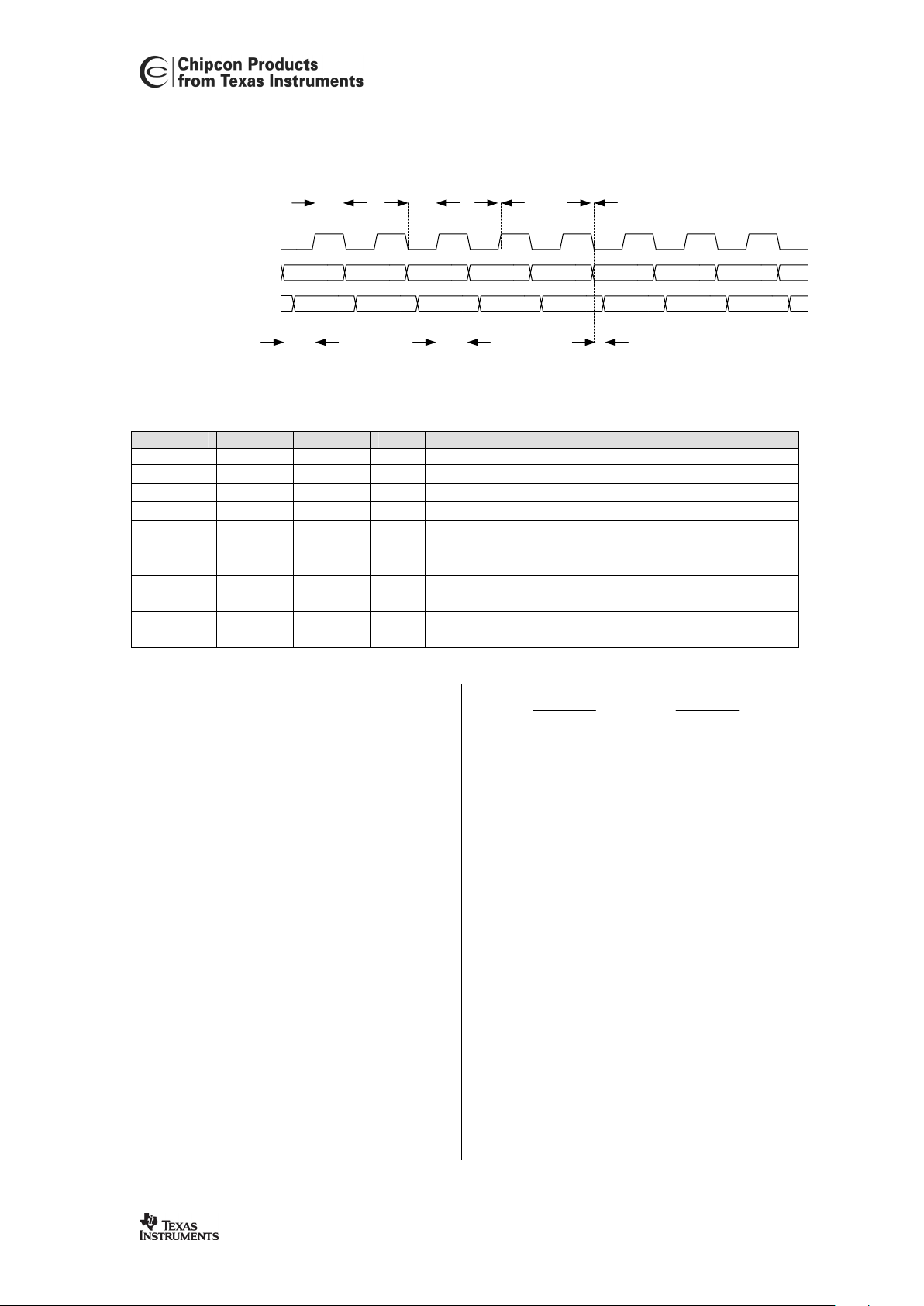
CC1010
SWRS047 Page 39 of 152
Figure 5. SPI Flash Programming Timing
Symbol Min Max Units Conditions
Fsck - f
XOSC
/ 8
Tsck, high
4 T
XOSC
-
The minimum time
SCK must be held high
Tsck, low
4 T
XOSC
-
The minimum time
SCK must be held low
Tsck, rise - T
XOSC
/2 ns
The maximum rise time on
SCK
Tsck, fall - T
XOSC
/2 ns
The maximum fall time on
SCK
Tsi, setup T
XOSC
-
The minimum setup time for
SI before the positive edge
on
SCK
Tsi, hold T
XOSC
-
The minimum hold time for
SI after the positive edge on
SCK
Tso, delay - T
XOSC
The delay from the negative edge on
SCK to valid data
on
SO
Table 17. SPI Flash Programming Timing Parameters
15.12.2 Programming Enable
Programming Enable is always the first
instruction to be sent. It must be sent to
synchronise the data flow and enable
CC1010
to receive further instructions.
Synchronisation is achieved when byte 2
of the instruction (0x53) is echoed back
from the SPI interface as byte 3. If
synchronisation is not achieved, byte 3 will
return all zeros. In this case, an extra clock
pulse should be inserted on
SCK, and the
Programming Enable instruction should be
resent. If synchronisation is not successful
within 32 attempts, Programming Enable
is unsuccessful and further debugging is
needed.
15.12.3 Set Flash Timing
The Set Flash Timing instruction is needed
to generate internal timing for the Flash
module.
FLTIM must be set in instruction
byte 4 so that:
MHz
f
MHz
f
XOSCXOSC
4.08.0
FLTIM
It is recommended to set
FLTIM to the
smallest number satisfying the equation
above, to reduce the time needed for
Flash programming. For a 3.6864 MHz
crystal,
FLTIM should be set to 5.
15.12.4 Chip Erase
The Chip Erase instruction erases all data
in the Flash memory, including the lock
bits. All bits will be set high.
Wait 450 ms (depending on Set Flash
Timing) after sending the Chip Erase
instruction before issuing a new
instruction.
15.12.5 Load Program Memory Page
The Load Program Memory Page
instruction is used to load the 128 bytes of
data in a page to a buffer in RAM. Each
instruction writes one byte to the 7 bit
address specified in the instruction.
SCK (P0.0)
SI (P0.1)
SO (P0.2)
7 6 5 4 3 2 1 0
7 6 5 4 3 2 1 0
Tsck, high Tsck, low
Tsck, rise Tsck, fall
Tsi, setup Tsi, hold Tso, delay
Page 40

CC1010
SWRS047 Page 40 of 152
15.12.6 Write Program Memory Page
The Write Program Memory Page
instruction writes the 128 bytes buffered
through the Load Program Memory Page
instructions to Flash memory.
After issuing this command, wait 5.4 ms
for it to complete. It is also possible to use
the Read Program Memory instruction to
poll when the program memory has been
written. When writing is in progress, all
read instructions will return 0xFF. Reading
an address containing data different from
0xFF can then be used to check when the
write is completed.
15.12.7 Read Program Memory
The Flash program memory can be read
back byte by byte using the Read Program
Memory instruction. The data is returned
in byte 4 of the instruction.
Wait at least 9 T
XOSC
between the last
negative transition on
SCK for byte 3
before issuing the first positive edge on
SCK for byte 4 to receive valid data.
15.12.8 Write Lock Bits
The reading (through SPI) and writing to
the Flash program memory can be
disabled by setting the lock bits as
described in this section. This should be
used for software protection.
The lock bits are set using the Write Lock
Bits instruction. A block of programmable
size at the top of the Flash program
memory can be locked for writing using
the
LSIZE bits. Page 0 can be
independently locked for writing by using
the
BBLOCK bit. Reading data through the
SPI interface can be disabled using the
SPIRE bit.
The detailed description of all lock bits is
given in Table 18.
Bit Name Function
7:3 - Reserved, write as '0'
4 BBLOCK Boot Block Lock
0 : Page 0 is write
protected
1 : Page 0 is writeable,
unless LSIZE is 000
3:1 LSIZE[2:0] Lock Size, sets the size of
the upper Flash area which
is write protected. Byte
sizes and page numbers
are listed below:
000 : 32768 (All pages)
001 : 16384 (page 128-
255)
010 : 8192 (page 192-255)
011 : 4096 (page 224-255)
100 : 2048 (page 240-255)
101 : 1024 (page 248-255)
110 : 512 (page 252-255)
111 : 0 (no pages)
0 SPIRE SPI Read Flash Enable /
Disable
0 : SPI Interface returns all
zeros on the Read
Program Memory
instruction
1 : SPI Interface returns
valid Flash data on the
Read Program Memory
instruction
Table 18. Flash Lock Bits
Lock bits can only be erased (set high) by
issuing the Chip Erase instruction. If
multiple Write Lock Bits instructions are
issued without chip erase in between,
each lock bit will be AND-ed together with
the previously written lock bits.
In effect, this means that it is not possible
to unlock the Flash program memory
without also erasing it.
The effect of the different lock size bits are
illustrated in Figure 6.
Page 41

CC1010
SWRS047 Page 41 of 152
0
1
2
126
127
128
129
130
190
191
192
193
194
222
223
224
225
226
238
239
240
241
242
246
247
248
249
250
251
252
253
254
255
Page number
Address
0x7FFF
0x7E00
0x7C00
0x7800
0x7000
0x6000
0x4000
0x0000
LSIZE = 000
LOCKED
LOCKEDUNLOCKED
LOCKEDUNLOCKED
LOCKEDUNLOCKED
LOCKEDUNLOCKED
UNLOCKED LOCKED
LOCKED
LSIZE = 001
LSIZE = 010
LSIZE = 011
LSIZE = 100
LSIZE = 101
LSIZE = 110
LSIZE = 111
UNLOCKED
UNLOCKED
Page 0 is locked when BBLOCK is cleared
Figure 6. Flash Lock Bits illustration
15.12.9 Read Lock Bits
The lock bits described in the previous
section can be read through the SPI
interface by using the Read Lock Bits
instruction. The instruction will return the 8
lock bits in byte 4 of the instruction.
Wait at least 9 T
XOSC
between the last
negative transition on
SCK for byte 3
before issuing the first positive edge on
SCK for byte 4 to receive valid data, as
with the Read Program Memory
instruction.
The lock bits can only be read through the
SPI interface, and not from the 8051 core.
15.12.10 Read Signature Byte
A 6 byte chip signature can be read
through the SPI interface using the Read
Signature Byte instruction. The 3 bit
signature byte address is issued, and the
value is then returned as byte 4.
Signature
byte address Value Meaing
000 0x7F
001 0x7F
010 0x7F
011 0x9E
JEDEC manufacturer
ID, identifies Chipcon
AS as the
manufacturer.
100 0x95 Identifies 32 kBytes
of Flash memory
101 0x00
Identifies
CC1010
Table 19. Signature Bytes
Wait at least 9 T
XOSC
between the last
negative transition on
SCK for byte 3
before issuing the first positive edge on
SCK for byte 4 to receive valid data, as
with the Read Program Memory
instruction.
15.12.11 SPI Flash Programming
Initialisation
CC1010
must be set into the Flash
programming mode to allow SPI Flash
operations. This is done as follows:
Apply power between all
DVDD and
DGND pins.
Hold
PROG low.
If a crystal is connected between
XOSC_Q1 and XOSC_Q2, hold RESET
low and wait for the oscillator to start
up. Crystal oscillator start-up times are
given in Table 10. Release
RESET
and wait at least 4 crystal oscillator
periods.
If a crystal is not connected between
XOSC_Q1 and XOSC_Q2, hold RESET
low and apply a clock signal to
XOSC_Q1. Release RESET after at
least 3 clock periods, and then wait at
least 4 clock periods.
Execute the Programming Enable
instruction to complete the SPI Flash
programming Initialisation.
CC1010
is now ready to be programmed, as
described in the next section.
Page 42

CC1010
SWRS047 Page 42 of 152
15.12.12 Programming the Flash Memory
After the initialisation is completed, SPI
programming can be performed as follows:
Device identity can be verified using
the Read Signature Byte instruction.
Perform Chip Erase.
Load one page into the buffer using
the Load Program Memory Page
instruction.
Write the buffer to Flash by using the
Write Program Memory Page
instruction.
Repeat the loading and writing of each
new page.
Programming can be verified using the
Read Program Memory instruction.
Set the lock bits using the Write Lock
Bits instruction.
Lock bits can be verified by using the
Read Lock Bits instruction.
15.13 8051 Flash Programming
Each of the 256 pages (128 bytes each) in
Flash program memory can be
programmed individually from the 8051.
The 8051 must be set in Idle Mode while
programming the Flash, since it has no
access to the program memory while the
writing is in progress.
The step for writing a page to Flash is
described as follows:
Set the correct write cycle time,
according to the current crystal
oscillator frequency, in the
FLTIM
SFR. This number is used to generate
the timing to the on-chip Flash
interface, as was also done with SPI
Flash programming. It must be set so
that:
MHz
f
MHz
f
XOSCXOSC
4.08.0
FLTIM
The time used for programming a
Flash page is strongly dependent on
the setting in
FLTIM. It is therefore
recommended to set
FLTIM as low as
possible, as with the SPI Flash
programming.
Write the desired Flash page number
to the
FLADR register.
Disable all interrupts except the Flash
/ Debug interrupt, which must be
enabled (through
EICON.FDIE).
Store the 128 bytes of data to be
written in the external data memory.
The address of the first byte in the
buffer must be a multiple of 128.
Write the 4 most significant bits of the
RAM buffer address to
FLCON.RMADR(3:0). Also set the bit
FLCON.WRFLASH.
Set the 8051 in Idle Mode by setting
PCON.IDLE. The Flash page is then
automatically erased and
programmed.
The sequence of the above steps is not
important. Flash programming is started
whenever entering Idle Mode while
FLCON.WRFLASH is set.
A Flash / Debug interrupt will be generated
when the page write operation is
completed, which will get the 8051 out of
Idle Mode. An ISR must be present to
service the Flash / Debug interrupt.
Page 43

CC1010
SWRS047 Page 43 of 152
FLADR (0xAE) - Flash Write Address Register
Bit Name R/W Reset value Description
7:0
FLADR(7:0)
R/W 0x00 The number of of the Flash page to be written (8 MSB
of the byte address)
FLCON (0xAF) - Flash Write Control Register
Bit Name R/W Reset value Description
7
-
R0 0 Reserved, read as 0
6:5
FLASH_LP
(1:0)
R/W 00 Flash Low Power control bits
00 : The Flash module is always active.
01 : The Flash module enters standby mode when the
8051 is put in Idle mode or Stop mode
10 : The Flash module enters standby mode between
instruction fetches and when the 8051 is put in Idle
Mode or Stop Mode.
11 : Reserved for future use.
4
WRFLASH
R/W 0 Write Flash Start bit
Starting a Flash page programming is done by first
setting this bit and then setting the 8051 in Idle Mode.
If the
WRFLASH bit is cleared before Idle Mode is
entered, no programming is performed.
3:0
RMADR(3:0)
R/W 0x0 RAM Buffer address
RMADR(3:0) contains the 4 most significant bits of
the RAM address where the data is buffered before
writing to Flash
FLTIM (0xDD) - Flash Write Timing Register
Bit Name R/W Reset value Description
7:0
FLTIM(7:0)
R/W 0x0A Flash Write Timing control
FLTIM must be set as described in this section prior
to using the 8051 Flash programming.
If an attempt is made to write data to a
Flash page which is locked (see the
previous section), a Flash / Debug
interrupt will be generated immediately
after Idle Mode is entered. No data will be
written.
It is not possible to read or write the Flash
lock bits from the 8051.
15.13.1 Example Code
Example C code writing data buffered at
address 0x100-0x17F in external RAM to
the second page in Flash (address 0x0800x0FF) is shown below. The system clock
frequency is assumed to be 3.6864 MHz.
An interrupt service routine must be
present at address 0x33, which clears the
interrupt flag
EICON.FDIF and returns
from the interrupt (RETI).
Page 44

CC1010
SWRS047 Page 44 of 152
FLTIM=0x05; /* Set Flash timing for 3.6864 MHz clock frequency */
FLADR=0x01; /* Write data to the second page in Flash */
EICON|=0x20; /* Enable Flash interrupt */
IE&= ~0x80; /* Disable other interrupts */
FLCON=0x10 | (0x100 >> 7);
/* Enable Flash writing, RAM buffer from addr. 0x100 */
PCON|=0x01; /* Enter Idle Mode to start Flash writing.
15.14 Flash Power Control
The Flash module can be set into different
power modes using the control bits
FLCON.FLASH_LP(1:0) introduced in
the previous section.
After reset, the Flash module is always
active, drawing a static current of
approximately 2.5 mA (at nominal
operating conditions). However, to save
power the Flash module can be set in a
power-down mode between instructions in
Active mode, and always in Idle or PowerDown mode. This will save approximately
1.5 mA of the Flash current consumption
during operation in Active mode, and 2.5
mA during Idle or Power-Down mode.
15.15 In Circuit Debugging
In order to facilitate a software monitor for
in-circuit debugging/emulation capabilities
a number of hardware support features
have been implemented:
A breakpoint instruction has been added
to the 8051's instruction set. The
instruction, given the mnemonic TRAP, is a
single byte instruction with the opcode
0xA5. In the original 8051 the 0xA5
opcode is executed as a NOP instruction
(opcode 0x00.) In the modified core this
instruction raises a highest-level interrupt
(Flash / Debug) by setting the
corresponding interrupt flag
EICON.FDIF
and waiting a sufficient number of
instruction cycles to allow the interrupt to
take effect before the next instruction.
The TRAP instruction can thus be written
over the first byte (opcode) of any other
instruction, the execution of which then will
result in a branch to a software debugging
monitor in the highest priority interrupt
service routine.
Single-stepping through instructions is
supported since exactly one instruction is
executed if an interrupt condition exists
when returning from an interrupt service
routine. Thus, single-stepping can be
accomplished simply by not clearing the
corresponding interrupt flag in the interrupt
service routine associated with the
software monitor.
A second serial port has been added to
enable debugging communication with a
host PC without disrupting applications
that use the main serial port for other
purposes.
Setting breakpoints and executing the
instructions which have a breakpoint
attached involves writing new data to the
Flash instruction memory several times.
Since the Flash memory can only
withstand 20000 (typical) erase/writecycles a simple instruction replacement
mechanism has been implemented. This
feature allows the surveillance of an
address in the instruction memory space
as defined in registers
RADRL and RADRH.
When this address is encountered on the
Flash program memory address bus, the
data returned on the data bus is replaced
by the contents of register
RDATA. Setting
RADRH=RADRL=0 disables the
replacement mechanism.
This instruction replacement mechanism
can be used in different ways:
A simple way of setting a single soft
(not stored in FLASH) breakpoint, by
setting
RDATA to 0xA5 (the TRAP
instruction) and
RADR to the
breakpoint address.
A simple way of restoring the original
opcode byte of an instruction which
has been subjected to a hard (stored
Page 45

CC1010
SWRS047 Page 45 of 152
in Flash) breakpoint, so that it can be
executed (in single-step mode).
SFRs (hardware registers) can
normally only be addressed directly
(i.e. by hardwiring the specific address
into the corresponding MOV
instruction.) This would make code in
a debug monitor, which returns the
value of SFRs to a PC rather bloated.
Using the instruction replacement
mechanism on the operand byte of the
move instruction instead of the opcode
byte, allows indirect addressing of
SFRs.
Chipcon provides software for in-circuit
debugging, which may be downloaded
from the Chipcon homepage. This
software uses the
RESERVED register,
which can then not be used for other
purposes. If in-circuit debugging is not
required, the
RESERVED register shown
below may be used for any purpose.
Writing to it will have no effect on the
operation of
CC1010
.
Great caution should be used when the
RADR is written. Since the address
consists of two bytes (
RADRL and RADRH),
there will be a short interval where the
address is not valid as only one of the
bytes are written at a time. If this
intermediate address point to the very
same location as of the code modifying the
RADR, a malfunction will occur. One
possible work-around is to first write
RADRH to a value pointing to a memory
location not used by the code.
RESERVED (0xE7) - Reserved register, used by Chipcon debugger software
Bit Name R/W Reset value Description
7:0
RESERVED(7:0)
R/W 0x00 Reserved register, which is used by Chipcon
debugger software. RESERVED may be used for
other purposes if Chipcon’s debugger software is
not needed.
RDATA (0xB9) - Replacement Data
Bit Name R/W Reset value Description
7:0
RDATA(7:0)
R/W 0x00 Replacement data.
Used to replace the byte at program memory
address
RADR with the data from RDATA, if
RADR
> 0.
RADRH (0xBB) - Replacement address, high byte
Bit Name R/W Reset value Description
7:0
RADR(15:8)
R/W 0x00 Replacement address, high byte.
Used to replace the byte at program memory
address
RADR with the data from RDATA, if
RADR
> 0.
RADRL (0xBA) - Replacement address, low byte
Bit Name R/W Reset value Description
7:0
RADR(7:0)
R/W 0x00 Replacement address, low byte.
Used to replace the byte at program memory
address
RADR with the data from RDATA, if
RADR
> 0
15.16 Chip Version / Revision
CC1010
has a SFR register CHVER that can
be read to decide the chip type and
current revision. The register description is
shown below.
Page 46

CC1010
SWRS047 Page 46 of 152
CHVER (0x9F) - Chip Version / Revision Register
Bit Name R/W Reset value Description
7:2
CHIP_TYPE
R 0x00
CHIP_TYPE is a read-only status word, which
gives the type number of the chip.
000000 :
CC1010
000001 - 111111 : Reserved for future use
1:0
CHIP_REV
R 0x01
CHIP_REV is a read only status word, which gives
the chip revision number of the chip. Current chip
revision is 01
Page 47

CC1010
SWRS047 Page 47 of 152
16. 8051 Peripherals
CC1010
offers the following peripherals
units controlled by the 8051-compatible
core:
Four general-purpose I/O ports, with
26 I/O pins in total.
Two standard 8051 timers
Two timers with PWM functionality
Watchdog timer
Real-time clock
SPI master
Hardware DES encryption / decryption
Random bit generator
10-bit ADC
These modules are described in the
following sections.
16.1 General Purpose I/O
Four general purpose I/O-ports are
available:
P0, P1, P2 and P3. Table 20
shows each port and the pins on each
port.
Each port is associated with two registers:
The port register (
P0, P1, P2, or P3) and
the direction register (
P0DIR, P1DIR,
P2DIR, or P3DIR).
Each bit in the
Px registers has its
associated bit in the direction registers
PxDIR. Setting PxDIR.y will make Px.y
an input which can be read in
Px(y). All
pins are inputs after reset. Clearing
PxDIR.y will make the pin Px.y output
the data from the register
Px(y). All Px
and
PxDIR register descriptions are
shown from page 49.
The structure for a single I/O-bit y on port
x is shown in Figure 7. Some ports have
alternate functions (such as the SPI
interface), which are enabled through
other registers (such as
SPCR.SPE).
These alternate functions may or may not
override the direction setting from
PxDIR
as shown.
When reading the
Px registers, data is
read from the directly from the pin. When
using a read-modify-write instruction such
as
ANL Px, #0x01, the output register
value is read and modified regardless of
the setting in
PxDIR.
Writing to the
Px registers writes to the
output register, and sets the I/O pin state.
Using a read-modify-write operation reads
from the output register, modifies the value
according to the instruction executed and
writes the result back into the output
register, modifying the I/O pin state
accordingly.
In practice, this means that the mov
instruction should only be used when
writing to all the pins in the port. To modify
only a few pins, use a read-modify-write
instruction. Also, be careful of using
constructs in C or another high-level
language that result in a mov from the
Px
registers, modify the result and write it
back (without using read-modify-write
instructions), as this will cause problems if
not all I/O pins in the port are configured
as outputs. In C, the |=, &= and ^=
operators should be used to set, clear and
toggle pins respectively.
The
CC1010
ports deviate from the
standard 8051-port in the following ways:
No pull-ups / pull-downs on pins
Dedicated direction bits in
PxDIR
registers
CMOS output levels on all ports
All general-purpose I/O pins are rated to
sink or source 2 mA, except pin P2.3,
which is rated to sink or source 8 mA.
Page 48

CC1010
SWRS047 Page 48 of 152
Alternate Function Port Available
pins
Normal operation Flash Programming
P0.0
SCK
, SPI Serial Clock output SCK, SPI Serial Clock Input
P0.1
MO
, SPI Master Output SI, SPI Slave Input
P0.2
MI
, SPI Master Input SO, SPI Slave Output
P0
P0.3 -
-
P1.0
- -
P1.1
- -
P1.2
- -
P1.3
- -
P1.4
- -
P1.5
- -
P1.6
- -
P1
P1.7
- -
P2.0
RXD1
, Serial port 1 input
-
P2.1
TXD1
, Serial port 1 output
-
P2.2
- -
P2.3
- -
P2.4
- -
P2.5
- -
P2.6
- -
P2
P2.7
- -
P3.0
RXD0
, Serial port 0 input
-
P3.1
TXD0
, Serial port 0 output
-
P3.2
INT0 , External interrupt 0
-
P3.3
INT1 , External interrupt 1
-
P3.4
T0
, Counter input 0 to Timer 0, or
PWM2, PWM output from Timer 2
-
P3
P3.5
T1
, Counter input 1 to Timer 1, or
PWM3, PWM output from Timer 3
-
Table 20. Available I/O-Ports
Page 49

CC1010
SWRS047 Page 49 of 152
Figure 7. Port x bit y structure
P0 (0x80) - Port 0 Data Register
Bit Name R/W Reset value Description
7
-
R0 0 Reserved, read as 0
6
-
R0 0 Reserved, read as 0
5
-
R0 0 Reserved, read as 0
4
-
R0 0 Reserved, read as 0
3
P0_3
R/W 1
2
P0_2
R/W 1
1
P0_1
R/W 1
0
P0_0
R/W 1
Data of port 0, bits 0 to 3.
P1 (0x90) - Port 1 Data Register
Bit Name R/W Reset value Description
7
P1_7
R/W 1
6
P1_6
R/W 1
5
P1_5
R/W 1
4
P1_4
R/W 1
3
P1_3
R/W 1
2
P1_2
R/W 1
1
P1_1
R/W 1
0
P1_0
R/W 1
Data of port 1, bits 0 to 7.
Alternate function enable
Alternate function static
direction or PxDIR.y
Alternate data
Read output register enable
PxDIR.y
DQInternal Data Bus
Read Pin Enable
S
1
0
S
1
0
Px.y PAD
Output register
Page 50

CC1010
SWRS047 Page 50 of 152
P2 (0xA0) - Port 2 Data Register
Bit Name R/W Reset value Description
7
P2_7
R/W 1
6
P2_6
R/W 1
5
P2_5
R/W 1
4
P2_4
R/W 1
3
P2_3
R/W 1
2
P2_2
R/W 1
1
P2_1
R/W 1
0
P2_0
R/W 1
Data of port 2, bits 0 to 7
P3 (0xB0) - Port 3 Data Register
Bit Name R/W Reset value Description
7
-
R0 0 Reserved, read as 0
6
-
R0 0 Reserved, read as 0
5
P3_5
R/W 1
4
P3_4
R/W 1
3
P3_3
R/W 1
2
P3_2
R/W 1
1
P3_1
R/W 1
0
P3_0
R/W 1
Data of port 3, bits 0 to 5
P0DIR (0xA4) - Port 0 Direction Register
Bit Name R/W Reset value Description
7
-
R0 0 Reserved, read as 0
6
-
R0 0 Reserved, read as 0
5
-
R0 0 Reserved, read as 0
4
-
R0 0 Reserved, read as 0
3
P0DIR_3
R/W 1
2
P0DIR_2
R/W 1
1
P0DIR_1
R/W 1
0
P0DIR_0
R/W 1
Port 0 direction register, bit 0 to 3. Each bit sets the
direction of the associated pin on Port 0.
0 : Associated pin is an output
1 : Associated pin is an input
P1DIR (0xA5) - Port 1 Direction Register
Bit Name R/W Reset value Description
7
P1DIR_7
R/W 1
6
P1DIR_6
R/W 1
5
P1DIR_5
R/W 1
4
P1DIR_4
R/W 1
3
P1DIR_3
R/W 1
2
P1DIR_2
R/W 1
1
P1DIR_1
R/W 1
0
P1DIR_0
R/W 1
Port 1 direction register, bit 0 to 7. Each bit sets the
direction of the associated pin on Port 1.
0 : Associated pin is an output
1 : Associated pin is an input
Page 51

CC1010
SWRS047 Page 51 of 152
P2DIR (0xA6) - Port 2 Direction Register
Bit Name R/W Reset value Description
7
P2DIR_7
R/W 1
6
P2DIR_6
R/W 1
5
P2DIR_5
R/W 1
4
P2DIR_4
R/W 1
3
P2DIR_3
R/W 1
2
P2DIR_2
R/W 1
1
P2DIR_1
R/W 1
0
P2DIR_0
R/W 1
Port 2 direction register, bit 0 to 7. Each bit sets the
direction of the associated pin on Port 2.
0 : Associated pin is an output
1 : Associated pin is an input
P3DIR (0xA7) - Port 3 Direction Register
Bit Name R/W Reset value Description
7
-
R0 0 Reserved, read as 0
6
-
R0 0 Reserved, read as 0
5
P3DIR_5
R/W 1
4
P3DIR_4
R/W 1
3
P3DIR_3
R/W 1
2
P3DIR_2
R/W 1
1
P3DIR_1
R/W 1
0
P3DIR_0
R/W 1
Port 3 direction register, bit 0 to 7. Each bit sets the
direction of the associated pin on Port 3.
0 : Associated pin is an output
1 : Associated pin is an input
Page 52

CC1010
SWRS047 Page 52 of 152
16.2 Timer 0 / Timer 1
CC1010
contains two standard 8051
timers/counters (Timer 0 and Timer 1)
which can operate as either a timer with a
clock rate based on the system clock (as
defined by the current clock mode), or as
an event counter clocked by the
T0 (P3.4
for Timer 0) or
T1 (P3.5 for Timer 1)
inputs.
Each Timer / Counter has a 16-bit register
which is readable and writeable through
TL0 and TH0 for Timer / Counter 0 and
TL1 and TH1 for Timer / Counter 1. These
registers are described below.
TL0 (0x8A) - Timer / Counter 0 Low byte counter value
Bit Name R/W Reset value Description
7:0
TL0(7:0)
R/W 0x00 Timer / Counter 0, low byte counter value
TL1 (0x8B) - Timer / Counter 1 Low byte counter value
Bit Name R/W Reset value Description
7:0
TL1(7:0)
R/W 0x00 Timer / Counter 1, low byte counter value
TH0 (0x8C) - Timer / Counter 0 High byte counter value
Bit Name R/W Reset value Description
7:0
TH0(7:0)
R/W 0x00 Timer / Counter 0, high byte counter value
TH1 (0x8D) - Timer / Counter 1 High byte counter value
Bit Name R/W Reset value Description
7:0
TH1(7:0)
R/W 0x00 Timer / Counter 1, high byte counter value
16.2.1 Timer / Counter 0 and 1 Modes
Timer / Counter 0 and 1 can individually
be programmed to operate in one out of
four different modes, controllable through
the registers
TMOD and TCON. They are as
follows:
13-bit timer / counter (Mode 0)
16-bit timer / counter (Mode 1)
8-bit timer / counter with auto-reload
(Mode 2)
Two 8-bit timers / counters (Mode 3,
Timer 0 only)
See the register descriptions for
TMOD and
TCON on the following pages.
Page 53

CC1010
SWRS047 Page 53 of 152
TMOD (0x89) - Timer / Counter 0 and 1 Mode register
Bit Name R/W Reset value Description
7
GATE1
R/W 0 Timer / Counter 1 gate control
0 : Timer / Counter 1 will clock only when TCON.TR1 is set.
1 : Timer / Counter 1 will clock only when
TCON.TR1 is set
and the INT0 input is high.
6
C/ T 1
R/W 0 Counter / Timer select for Counter / Timer 1
0 : Timer 1 is clocked by the system clock divided by 4 or 12,
depending on the state of
CKCON.T1M (see page 55)
1 : Timer 1 is clocked by the
T1 pin.
5
M1.1
R/W 0
4
M1.0
R/W 0
Timer / Counter 1 mode select bits
00 : 13-bit counter
01 : 16-bit counter
10 : 8-bit counter with auto-reload
11 : Timer 1 off
3
GATE0
R/W 0 Timer / Counter 0 gate control
0 : Timer / Counter 0 will clock only when
TCON.TR0 is set.
1 : Timer / Counter 0 will clock only when
TCON.TR0 is set
and the INT0 input is high.
2
C/ T 0
R/W 0 Counter / Timer select for Counter / Timer 0
0 : Timer 0 is clocked by the system clock divided by 4 or 12,
depending on the state of
CKCON.T0M (see page 55)
1 : Timer 0 is clocked by the
T0 pin.
1
M0.1
R/W 0
0
M0.0
R/W 0
Timer / Counter 0 mode select bits
00 : 13-bit counter
01 : 16-bit counter
10 : 8-bit counter with auto-reload
11 : Two 8-bit counters
Page 54

CC1010
SWRS047 Page 54 of 152
TCON (0x88) - Timer / Counter 0 and 1 control register
Bit Name R/W Reset value Description
7
TF1
R/W 0
Timer 1 overflow flag.
TF1 is set to 1 by hardware when the
Timer 1 count overflows and is cleared by hardware when the
8051 vectors to the interrupt service routine.
6
TR1
R/W 0 Timer 1 run control bit
0 : Timer / Counter 1 is disabled
1 : Timer / Counter 1 is enabled
5
TF0
R/W 0
Timer 0 overflow flag.
TF0 is set to 1 by hardware when the
Timer 0 count overflows and is cleared by hardware when the
8051 vectors to the interrupt service routine.
4
TR0
R/W 0 Timer 0 run control bit
0 : Timer / Counter 0 is disabled
1 : Timer / Counter 0 is enabled
3
IE1
R/W0 0 External interrupt 1 edge detect (interrupt flag)
If external interrupt 1 is configured to be edge sensitive
(TCON.IT1 = 1), IE1 is set by hardware when a negative
edge is detected on the
INT1 pin and is cleared by hardware
when the 8051 vectors to the corresponding interrupt service
routine. In edge-sensitive mode,
IE1 can also be set by
software.
If external interrupt 1 is configured to be level-sensitive
(
TCON.IT1 = 0), IE1 is set when the INT1 pin is low and
cleared when the
INT1 pin is high. In level-sensitive mode,
software cannot write to
IE1.
2
IT1
R/W 0 External interrupt 1 type select.
0 : The
INT1 interrupt is triggered when INT1 is low (level
sensitive).
1 : The INT1 interrupt is triggered on the falling edge (edge
sensitive)
1
IE0
R/W0 0 External interrupt 0 edge detect (interrupt flag)
If external interrupt 0 is configured to be edge sensitive
(
TCON.IT0 = 1), IE0 is set by hardware when a negative
edge is detected on the
INT0 pin and is cleared by hardware
when the 8051 vectors to the corresponding interrupt service
routine. In edge-sensitive mode,
IE0 can also be set by
software.
If external interrupt 0 is configured to be level-sensitive
(TCON.IT0 = 0), IE0 is set when the INT0 pin is low and
cleared when the
INT0 pin is high. In level-sensitive mode,
software cannot write to
IE0.
0
IT0
R/W 0 External interrupt 0 type select.
0 : The
INT0 interrupt is triggered when INT0 is low (level
sensitive).
1 : The
INT0 interrupt is triggered on the falling edge (edge
sensitive)
Page 55

CC1010
SWRS047 Page 55 of 152
CKCON (0x8E) - Timer Clock rate Control Register
Bit Name R/W Reset value Description
7
-
R0 0 Reserved, read as 0
6
-
R0 0 Reserved, read as 0
5
-
R0 0 Reserved, read as 0
4
T1M
R/W 0
Timer 1 clock select.
T1M has no effect in counter mode.
0 : Timer 1 uses the C clock divided by 12 (for
compatibility with the 80C32)
1 : Timer 1 uses the C clock divided by 4
3
T0M
R/W 0
Timer 0 clock select.
T0M has no effect in counter mode.
0 : Timer 0 uses the C clock divided by 12 (for
compatibility with the 80C32)
1 : Timer 0 uses the C clock divided by 4
2:0
MD(2:0)
R/W 001
MD(2:0) controls the memory stretch cycles when
accessing the external RAM. The reset value is 001, but
for faster access to external RAM, MD(2:0) should
always be written 000.
16.2.2 Mode 0
Mode 0 operation is illustrated for timer or
counter 0 and 1 in Figure 8. The timer /
counter uses bit 0 to 4 of
TL0 / TL1 and all
8 bits of
TH0 / TH1 as a 13 bit counter.
TCON.TR0 / TCON.TR1 must be set to
enable the Timer / Counter.
The
TC/ bit in TMOD selects the Timer or
Counter clock source as described.
Transitions are counted from the selected
source, as long as
TMOD.GATE0 /
TMOD.GATE1 is 0, or TMOD.GATE0 /
TMOD.GATE1 is 1 and the corresponding
interrupt pin (
INT0 / INT1 ) is
deasserted.
When the 13-bit count increments from
0x1FFF (all ones), the counter rolls over to
all zeros. The overflow flag
TCON.TF0 /
TCON.TF1 is then set.
The 3 most significant bits in
TL0 / TL1
are undetermined in Mode 0, and should
be masked by software for evaluation.
In Mode 0, the timer timeout period is
determined by:
xosc
f
TLxTHxTxMCKCON
T
:8192.812
where THx:TLx is the contents of the
THx:TLx registers if this is reloaded in the
interrupt handler, or 0 if no reload is done.
Page 56

CC1010
SWRS047 Page 56 of 152
System Clk
Divide by 12
Divide by 4
0
1
T0 / T1
T0M / T1M
0
1
C/T0 / C/T1
TR0 / TR1
GATE0 / GATE1
INT0 / INT1
TL0 / TL1
01234567
TH0 / TH1
01234567
Mode 0
Mode 1
TF0 / TF1
Timer 0 / Timer 1
interrupt request
Clock
Figure 8. Mode 0 and Mode 1 operation for Timer / Counter 0 or 1
16.2.3 Mode 1
Mode 1 operation is illustrated for Timer /
Counter 0 and 1 in Figure 8. The counter
is configured as a 16-bit counter, as
compared to the 13 bits in Mode 0, and all
bits in
TL0 or TL1 are thus used. The
counter overflows when the count
increments from 0xFFFF.
Otherwise, Mode 1 operation is the same
as Mode 0.
In Mode 1, the timer timeout period is
determined
by:
xosc
f
TLxTHxTxMCKCON
T
:65536.812
where THx:TLx is the contents of the
THx:TLx registers if this is reloaded in the
interrupt handler, or 0 if no reload is done.
16.2.4 Mode 2
Mode 2 operation is illustrated for Timer /
Counter 0 and 1 in Figure 9. Mode 2
operates as an 8-bit counter with
automatic reload of the start value.
The Timer / Counter is controlled as for
Mode 0 and Mode 1, but when
TL0 / TL1
overflows,
TH0 / TH1 is loaded into TL0 /
TL1.
In Mode 2, the timer timeout period is
determined by:
xosc
f
THxTxMCKCON
T
256.812
Page 57

CC1010
SWRS047 Page 57 of 152
System Clk
Divide by 12
Divide by 4
0
1
T0 / T1
T0M / T1M
0
1
C/T0 / C/T1
TR0 / TR1
GATE0 / GATE1
INT0 / INT1
TL0 / TL1
TH0 / TH1
TF0 / TF1
Timer 0 / Timer 1
interrupt request
Clock
Mux
Reload
Figure 9. Mode 2 operation for Timer / Counter 0 or 1
16.2.5 Mode 3
In Mode 3, which is illustrated in Figure 10,
Timer 0 is operated as two separate 8-bit
counters and Timer 1 stops counting and
holds its value.
TL0 is configured as an 8-bit counter
controlled by the normal Timer 0 control
bits. It counts either clock cycles divided
by 4 or by 12 (as given by
CKCON.T0M), or
high to low transitions on
T0 (as given by
TMOD.C/ T 0). It is also possible to use
the
GATE function for TL0 to set INT0 as
count enable.
TH0 is locked into a timer function, and
takes over the use of
TR1 and TF1 from
Timer 1. It counts clock cycles divided by 4
or 12 (as given by
CKCON.T1M). TH0 may
then generate Timer 1 interrupts.
Timer 1 has limited usage when Timer 0 is
in mode 3. This is because Timer 0 uses
the Timer 1 control bit
TR1 and the
interrupt flag
TF1. However, Timer 1 can
still be used for baud rate generation and
the Timer 1 count values are still available
in the
TL1 and TH1 registers.
Control of Timer 1 when Timer 0 is in
mode 3 is done through the Timer 1 mode
bits. To turn Timer 1 on, set Timer 1 to
mode 0, 1 or 2. To turn Timer 1 off, set it
to mode 3. Timer 1 can count clock cycles
divided by 4 or 12 or high to low transitions
on the
T1 pin. The GATE function is also
available.
In Mode 3, the timer timeout periods are
determined by:
xosc
f
TYxTxMCKCON
T
256.812
where TYx is the contents of the THx or
TLx register if this is reloaded in the
interrupt handler, or 0 if no reload is done.
Page 58

CC1010
SWRS047 Page 58 of 152
C Clk
Divide by 12
Divide by 4
0
1
T0
T0M
0
1
C/T0
TR0
GATE0
INT0
TL0
TF0
Timer 0 interrupt
request
Clock
TH0
TF1
Timer 1 interrupt
request
TR1
Clock
Figure 10. Mode 3 operation for Timer / Counter 0
Page 59

CC1010
SWRS047 Page 59 of 152
16.3 Timer 2 / 3 with PWM
CC1010
also features two timers with pulse
width modulation (PWM) outputs. Each
timer can generate interrupts, as
described in the Interrupts section on page
28. The timers are individually set in one
of two modes, timer mode or PWM mode.
This is controlled through the bits
M2 and
M3 in the TCON2 control register shown
below.
Timer 2 and Timer 3 are enabled
individually through the bits
TCON2.TR2
and
TCON2.TR3.
TCON2 (0xA9) - Timer Control register 2
Bit Name R/W Reset value Description
7
-
R0 0 Reserved, read as 0
6
-
R0 0 Reserved, read as 0
5
-
R0 0 Reserved, read as 0
4
-
R0 0 Reserved, read as 0
3
TR3
R/W 0 Timer 3 run control
0 : Timer 3 is disabled. The Timer 3 counter is cleared.
1 : Timer 3 is enabled.
2
M3
R/W 0 Timer 3 mode control.
0 : Timer 3 is in timer mode.
1 : Timer 3 is in PWM mode.
P3.5 is set to be an output,
overriding
P3DIR(5)
1
TR2
R/W 0 Timer 2 run control
0 : Timer 2 is disabled. The Timer 2 counter is cleared.
1 : Timer 2 is enabled.
0
M2
R/W 0 Timer 2 mode control.
0 : Timer 2 is in timer mode.
1 : Timer 2 is in PWM mode.
P3.4 is set to be an output,
overriding
P3DIR(4)
16.3.1 Timer Mode
Timer 2 / Timer 3 can be set in Timer
Mode by clearing the bit
TCON2.M2 /
TCON2.M3. Timer Mode operation is
illustrated in Figure 11. The 16 bit counter
is preloaded with
T2 and T2PRE (or T3
and
T3PRE) as shown. When disabling the
timer through clearing
TCON2.TR2 (or
TCON2.TR3) the counter is also
preloaded. The counter value cannot be
read by software.
When the counter underflows (decrements
from a zero value), it is loaded with the
contents of
T2 / T3 and T2PRE / T3PRE,
and the interrupt request bit
EXIF.TF2 /
EXIF.TF3 is set by hardware. The
interrupt request must be cleared by
software.
In Timer mode, interrupts are generated
with an interval as given by T
nINT
, where
n2,3 :
system
nInt
f
T
1256255
TnTnPRE
As long as
TnPRE and Tn are set before
TCON.TRn, the first interrupt is generated
T
nINT
after enabling the timer and then with
T
nINT
intervals.
Page 60

CC1010
SWRS047 Page 60 of 152
Figure 11. Timer Mode operation for Timer 2 / Timer 3
T2PRE (0xAA) - Timer 2 Prescaler Control
Bit Name R/W Reset value Description
7:0
T2PRE(7:0)
R/W 0x00 Timer 2 Prescaler Control.
In Timer Mode,
T2PRE sets the 8 most significant bits of
the 16-bit counter reload value. In PWM Mode,
T2PRE
sets the prescaler value that sets the PWM period.
T3PRE (0xAB) - Timer 3 Prescaler Control
Bit Name R/W Reset value Description
7:0
T3PRE(7:0)
R/W 0x00 Timer 3 Prescaler Control.
In Timer Mode, T3PRE sets the 8 most significant bits of
the 16-bit counter reload value. In PWM Mode,
T3PRE
sets the prescaler value that sets the PWM period.
T2 (0xAC) - Timer 2 Low byte counter value
Bit Name R/W Reset value Description
7:0
T2(7:0)
R/W 0x00
In Timer Mode,
T2 sets the 8 least significant bits of the
16-bit counter reload value. In PWM Mode
T2 sets the
PWM duty cycle.
T3 (0xAD) - Timer 3 Low byte counter value
Bit Name R/W Reset value Description
7:0
T3(7:0)
R/W 0x00
In Timer Mode,
T3 sets the 8 least significant bits of the
16-bit counter reload value. In PWM Mode
T3 sets the
PWM duty cycle.
16.3.2 PWM Mode
Timer 2 /Timer 3 can be set in PWM Mode
by setting the bit
TCON2.M2 / TCON2.M3.
The pins
P3.4 / P3.5 are then enabled as
outputs, overriding the port direction bit
P3DIR.4 / P3DIR.5. The port direction is
overridden independent of the timer run
control bit
TCON2.TR2 / TCON2.TR3.
Interrupts are not generated in PWM
mode.
P3.4 is the PWM output for timer 2, P3.5
is the PWM output for Timer 3.
The PWM operation is illustrated in Figure
13. The PWM period T
nPWM
for timer n is
set by
TnPRE:
system
nPWM
f
T
1255
TnPRE
Divide
by 255
Timer 2 (or Timer 3)
16 bit counter
EXIF.TF2
(or EXIF.TF3)
Timer 2
(or Timer 3)
interrupt request
Clk
Mux
Mux
0
123456 7 8 9 10 11 12 13 14 15
0
123456701234567
T2 (or T3) T2PRE (or T3PRE)
Underflow
TR2
(or TR3)
System
Clock
Page 61

CC1010
SWRS047 Page 61 of 152
The PWM “high” state duration T
nhPWM
for
timer n is set by
Tn:
system
nhPWM
f
T
)1(
TnPRETn
This means that in PWM mode, setting
Tn
to 0 produces a constant low output and
setting
Tn to 255 produces a constant high
output. The timing of the PWM outputs is
illustrated in Figure 12.
PWMn
Output
T
nPWM
T
nPWM
T
nhPWM
T
nhPWM
Figure 12. PWM Timing illustration
System Clk
Divide by
TnPRE + 1
8 bit counter
(counts 0-254)
A>B?
PWM output
TnPWM
A
B
Timer 2 or Timer 3
Figure 13. PWM operation for Timer 2 / Timer 3
Page 62

CC1010
SWRS047 Page 62 of 152
16.4 Power On Reset (Brown-Out Detection)
The Power On Reset functionality detects
power-on and brown-out situations, and
includes glitch immunity and hysteresis for
noise and transient stability.
The power on reset functionality is
disabled using the dedicated POR_E pin.
Grounding POR_E will disable the internal
power on reset. An external power-on-
reset module should then be connected to
the external
RESET pin.
The Power On Reset and Brown-Out
Detection voltage levels are specified in
the Electrical Specifications section at
page 7.
Page 63

CC1010
SWRS047 Page 63 of 152
16.5 Watchdog Timer
CC1010
includes an 8-bit watchdog timer
that is clocked by the system clock. The
clock is divided by a number in the range
from 2048 to 16384, controllable through
WDT.WDTPRE(1:0). The divided clock
controls an 8-bit timer, which generates
system reset upon overflow. A block
diagram for the Watchdog Timer is shown
in Figure 14.
Chipcon recommends that the watchdog
timer should be disabled when the
CC1010
is clocked from the 32 kHz oscillator
(Clock mode 1).
Note that the watchdog timer is not active
in Power-down mode, and therefore
cannot wake up the
CC1010
from Power-
Down mode.
WDT (0xD2) - Watchdog Timer Control Register
Bit Name R/W Reset value Description
7
-
R0 0 Reserved, read as 0
6
-
R0 0 Reserved, read as 0
5
-
R0 0 Reserved, read as 0
4
WDTSE
R/W 0 Watchdog Timer Stop Enable, used to disable the
watchdog timer
3
WDTEN
R/W 1 Watchdog Timer Enable / Disable
0 : The watchdog timer is disabled
1 : The watchdog timer is enabled
The watchdog timer is enabled after reset. To disable the
watchdog timer,
WDTSE must be used as described in this
section.
2
WDTCLR
R0/W 0
Watchdog timer clear signal.
WDTCLR must periodically
be set to prevent the watchdog timer from resetting the
system.
WDTCLR is cleared by hardware, and is thus
always read 0.
0 : Normal watchdog operation
1 : Watchdog timer is cleared.
1:0
WDTPRE.1
R/W 11
Watchdog timer prescaler control.
WDTPRE(1:0)
controls the division of the main crystal oscillator clock to
generate the watchdog timer clock.
00 : f
WDT
= f
XOSC
/ 2048
01 : f
WDT
= f
XOSC
/ 4096
10 : f
WDT
= f
XOSC
/ 8192
11 : f
WDT
= f
XOSC
/ 16384
Page 64

CC1010
SWRS047 Page 64 of 152
System clock Watchdog Prescaler
/2048
/4096
/8192
/16384
WDTPRE(1:0)
8 Bit Watchdog Counter
Overflow
WDTEN
System
Reset
Clear
Clear
Enable
Enable
WDTCLR
Figure 14. Watchdog Timer
Setting different prescaler settings,
combined with different Main Crystal
Oscillator frequencies, generates reset at
an interval of:
system
WDTPRE
f
)11(
2256
The intervals for the maximum and
minimum clock frequencies are shown in
Table 21 below.
WDTPRE.1 WDTPRE.0 Division Rate Reset timing, given
f
XOSC
= 3MHz
Reset timing, given
f
XOSC
= 24MHz
0 0 2048 175 ms 21.8 ms
0 1 4096 350 ms 43.7 ms
1 0 8192 699 ms 87.4 ms
1 1 16384 1400 ms 175 ms
Table 21. Watchdog Timer timing
16.5.1 Disabling the Watchdog Timer
The Watchdog Timer is enabled after
system reset, through the Watchdog Timer
enable flag
WDT.WDTEN. To disable the
Watchdog Timer, this flag must be
cleared. However, clearing this flag
requires the user to first set the flag
WDT.WDTSE, and then clearing
WDT.WDTEN within 16 system clock
periods (preferably in the next instruction).
If interrupts are enabled while disabling
the Watchdog Timer, the user must make
sure that
WDT.WDTEN is actually cleared.
This could for instance be done as follows:
Page 65

CC1010
SWRS047 Page 65 of 152
while (WDT & 0x08) {
WDT |= 0x10; // Set WDTSE
WDT &= ~0x08; // Clear WDTEN
}
16.5.2 Enabling the Watchdog Timer
Enabling the Watchdog Timer is simply
done by setting
WDT.WDTEN. Using the
WDT.WDTSE control bit is not required.
16.6 Real-time Clock
The real-time clock can generate
interrupts with intervals ranging from 1 to
127 seconds. It is connected to the 32.768
kHz crystal oscillator, which is disabled
after reset. It must be enabled as
described in the section on page 33. An
external 32.768 kHz clock signal can also
be applied, as described.
The interrupt interval is programmed in the
range from 1 through 127 seconds by
setting
RTCON.RT(6:0). The timer is
enabled by setting
RTCON.RTEN. The first
interrupt will be generated
RT seconds
after
RTEN is set.
The real-time clock interrupt must be
enabled as described in the Interrupts
section on page 28.
The RTC oscillator circuit is shown in
Figure 15. The loading capacitors values
can be calculated as described for the
main crystal oscillator at page 32.
RTCON (0xED) – Real-time Clock Control Register
Bit Name R/W Reset value Description
7
RTEN
R/W 0 Real-time Clock Enable / Disable
0 : Real-time Clock is disabled
1 : Real-time Clock is enabled
6:0
RT(6:0)
R/W 0x00
Real-time Clock interrupt interval control.
RT(6:0) gives
the desired interrupt interval in seconds.
RT(6:0) must be
between 1 and 127.
C13C12
XTAL
32.768 kHz
XTAL
32.768 kHz
XOSC32_Q1 XOSC32_Q2
Figure 15. RTC oscillator circuit
Page 66

CC1010
SWRS047 Page 66 of 152
16.7 Serial Port 0 and 1
Two serial ports, serial port 0 and 1, are
implemented. They are controlled through
the
SCON0 and SCON1 control register.
The data is buffered in
SBUF0 and SBUF1.
Serial port 0 may be used for general
purpose serial communication. Timer 1
may be used to generate different baud
rates. Serial port 1 is primarily for use with
an in-circuit-debugger, but can also be
used for general purpose serial
communication. A block diagram is shown
in Figure 16.
The general-I/O ports that map to the
same physical pins as the serial ports
must be configured in a certain way in
order to allow serial communication. This
is summarized in Table 22.
The mode is set in
SCON0.SMx_0 /
SCON1.SMx_0. To receive data,
SCON0.REN_0 / SCON1.REN_1 must be
enabled for the ports. Separate transmit
and receive interrupt flags are available in
SCON0.TI_0 / RI_0 and SCON1.TI_1 /
RI_1. Note that the baud rate also
depends on the Clock Mode selected (see
page 35).
SCON0/SCON1
Receive
Shift Register
SBUF0/SBUF1
(Receive)
SBUF0/SBUF1
(Transmit)
Interrupt
Request
RI_0/RI_1 TI_0/TI_1
Read SBUF
Write SBUF
TXD0/TXD1
Load SBUF
Mode 0
Transmit
RXD0/RXD1
Data Bus
Figure 16. Serial ports block diagram
UART0 UART1
P3.0 P3.1 P3DIR.0 P3DIR.1 P2.0 P2.1 P2DIR.0 P2DIR.1
Mode 0
x 1 1 0 x 1 1 0
RX
Mode 1-3
x x 1 x x x 1 x
Mode 0
1 1 0 0 1 1 0 0
TX
Mode 1-3
x 1 x 0 x 1 x 0
Table 22. Configuration of general purpose I/O for UART0 and UART1
Page 67

CC1010
SWRS047 Page 67 of 152
SBUF0 (0x99) - Serial Port 0, data buffer
Bit Name R/W Reset value Description
7:0
SBUF0(7:0)
R/W 0x00 Serial Port 0, data buffer.
SBUF1 (0xC1) – Serial Port 1, data buffer
Bit Name R/W Reset value Description
7:0
SBUF1(7:0)
R/W 0x00 Serial Port 1, data buffer
SCON0 (0x98) - Serial Port 0 Control Register
Bit Name R/W Reset value Description
7
SM0_0
R/W 0
6
SM1_0
R/W 0
Serial Port 0 mode bits, decoded as:
SM0_0 SM1_0 Mode
0 0 0 (Synchronous half duplex)
0 1 1 (Asynchronous full duplex, start + stop bit)
1 0 2 (Asynchronous full duplex, start + stop bit,
9th data bit)
1 1 3 (Asynchronous full duplex, start + stop bit,
9th data bit)
5
SM2_0
R/W 0 Multiprocessor communication enable. In modes 2 and 3
SM2_0 = 1 enables the multiprocessor communication feature:
In mode 2 or 3
RI_0 will not be activated if the received 9th bit
is 0. If
SM2_0 = 1 in mode 1, RI_0 will only be activated if a
valid stop bit is received. In mode 0
SM2_0 establishes the
baud rate: when
SM2_0 = 0 the baud rate is clk / 12; when
SM2_0 = 1 the baud rate is clk / 4.
4
REN_0
R/W 0
Receive enable. When
REN_0 = 1 reception is enabled.
3
TB8_0
R/W 0 Defines the state of the 9th data bit transmitted in modes 2 and
3.
2
RB8_0
R/W 0
In modes 2 and 3
RB8_0 indicates the state of the 9th bit
received. In mode 1
RB8_0 indicates the state of the received
stop bit. In mode 0
RB8_0 is not used.
1
TI_0
R/W 0 Transmit interrupt flag. Indicates that the transmit data word
has been shifted out. In mode 0 TI_0 is set at the end of the
8th data bit. In all other modes
TI_0 is set when the stop bit is
placed on the
TXD0 pin. TI_0 must be cleared by the
software.
0
RI_0
R/W 0 Receive interrupt flag. Indicates that a serial data word has
been received. In mode 0
RI_0 is set at the end of the 8th
data bit. In mode 1
RI_0 is set after the last sample of the
incoming stop bit, subject to the state of
SM2_0. In modes 2
and 3
RI_0 is set at the end of the last sample of RB8_0.
RI_0 must be cleared by the software.
Page 68

CC1010
SWRS047 Page 68 of 152
SCON1 (0xC0) - Serial Port 1 Control Register
Bit Name R/W Reset value Description
7
SM0_1
R/W 0
6
SM1_1
R/W 0
Serial Port 1 mode bits, decoded as:
SM0_1 SM1_1 Mode
0 0 0 (Synchronous half duplex)
0 1 1 (Asynchronous full duplex, start + stop bit)
1 0 2 (Asynchronous full duplex, start + stop bit,
9th data bit)
1 1 3 (Asynchronous full duplex, start + stop bit,
9th data bit)
5
SM2_1
R/W 0 Multiprocessor communication enable. In modes 2 and 3
SM2_1 = 1 enables the multiprocessor communication feature:
In mode 2 or 3
RI_1 will not be activated if the received 9th bit
is 0. If
SM2_1 = 1 in mode 1 RI_1 will only be activated if a
valid stop bit is received. In mode 0
SM2_1 establishes the
baud rate: when
SM2_1 = 0 the baud rate is clk / 12; when
SM2_1= 1 the baud rate is clk / 4.
4
REN_1
R/W 0
Receive enable. When
REN_1 = 1 reception is enabled.
3
TB8_1
R/W 0 Defines the state of the 9th data bit transmitted in modes 2 and
3.
2
RB8_1
R/W 0
In modes 2 and 3
RB8_1 indicates the state of the 9th bit
received. In mode 1
RB8_1 indicates the state of the received
stop bit. In mode 0
RB8_1 is not used.
1
TI_1
R/W 0 Transmit interrupt flag. Indicates that the transmit data word
has been shifted out. In mode 0 TI_1 is set at the end of the
8th data bit. In all other modes
TI_1 is set when the stop bit is
placed on the
TXD1 pin. TI_1 must be cleared by the
software.
0
RI_1
R/W 0 Receive interrupt flag. Indicates that a serial data word has
been received. In mode 0
RI_1 is set at the end of the 8th
data bit. In mode 1
RI_1 is set after the last sample of the
incoming stop bit, subject to the state of
SM2_1. In modes 2
and 3
RI_1 is set at the end of the last sample of RB8_1.
RI_1 must be cleared by the software.
16.7.1 MODE 0
Serial mode 0 provides synchronous, halfduplex serial communication. For serial
port 0, pin
RXD0 (P3.0) is used for data
input and output while
TXD0 (P3.1)
provides the bit clock for both transmit and
receive. For serial port 1 the
corresponding pins are
RXD1 (P2.0) and
TXD1 (P2.1).
The serial mode 0 baud rate is set by
SCON0.SM2_0 / SCON1.SM2_1. If this bit
is cleared, the baud rate is the system
clock divided by 4. If the bit is set, the
system clock is divided by 12.
Data transmission begins when an
instruction writes to the
SBUF0 (or SBUF1)
register. The serial port shifts the data byte
out, LSB first, at the selected baud rate.
Data reception starts when
SCON0.REN_0
/
SCON1.REN_1 is set and the receive
interrupt flag
SCON0.RI_0 / SCON1.RI_1
is cleared. The bit clock is activated and
the UART shifts data in on each rising
edge of the bit clock, until 8 bits have been
received. Immediately after the 8th bit is
shifted in, the receive interrupt flag is set
and reception stops until the software
clears the flag.
Page 69

CC1010
SWRS047 Page 69 of 152
The clock output is high when the serial
port is idle. In reception, data is shifted in
on the rising edge of the clock. In
transmission, each new bit is set on the
falling edge of the clock.
T1M/TH1 Baudrate
(kBaud)
F
xosc
=
3.6864
MHz
F
xosc
=
7.3728
MHz
F
xosc
=
11.0592
MHz
F
xosc
=
14.7456
MHz
F
xosc
=
18.4320
MHz
F
xosc
=
22.1184
MHz
57.6 1/255 1/254 0/255 1/252 1/251 1/250
19.2 1/253 1/250 0/253 0/252 1/241 1/238
9.6 1/250 1/244 0/250 0/248 1/226 1/220
4.8 1/244 1/232 0/244 0/240 1/196 1/184
2.4 1/232 1/208 0/232 0/224 1/136 1/112
1.2 1/208 1/160 0/208 0/192 1/16 0/160
Table 23. Baud rate examples (SMODx=1)
16.7.2 MODE1
Mode 1 provides standard asynchronous
full duplex communication, using a total of
10 bits: 1 start bit, 8 data bits and 1 stop
bit. For receive operations, the stop bit is
stored in
SCON0.RB8_0 (or
SCON1.RB8_1). Data bits are received
and transmitted with their LSB first.
The baud rate for mode 1 is a function of
timer 1 overflow. Each time the timer
increments from its maximum count
(0xFF), a clock pulse is sent to the baud
rate circuit, to be further divided by 16 or
32 as set by
PCON.SMOD0 /
EICON.SMOD1 to give the baud rate:
overflowTimerRateBaud 1
32
2
SMODx
As can be seen from the equation above,
if both serial ports are in use
simultaneously, the baud rate is equal or
different by a factor 2.
It is common to use Timer 1 in Mode 2 (8bit counter with auto-reload) for baud rate
generation, although any timer mode can
be used. The Timer 1 reload value is
stored in the
TH1 register, which makes
the complete baudrate using mode 2:
)256()812(32
2
TH1T1M
SMODx
system
f
RateBaud
T1M in the above equation is in register
CKCON (see page 55), and controls the
initial division in Timer 1 between 4 and
12.
Some example baud rates and reload
values are shown in Table 23. The setting
for other baud rates and oscillator
frequencies can be determined by using
the above equation.
To transmit data in mode 1, write data to
SBUF0 / SBUF1. Transmission is then
performed on
TXD0 / TXD1 in the following
order: start bit, 8 data bits (LSB first) and
then the stop bit.
Reception begins on the falling edge of a
start bit received on
RXD0 / RXD1, if
reception is enabled in
SCON0.REN_0 /
SCON1.REN_1. The data input is sampled
16 times per baud for any baud rate. Each
bit decision is performed as a majority
decision between 3 successive samples in
the middle of each baud. If the majority
decision is not equal to zero for the start
bit, the serial port will stop reception and
wait for a new start bit.
When the majority decision is made for the
stop-bit, the following conditions must be
met:
RI_0 / RI_1 is 0
If
SM2_0 / SM2_1 is set, the state of
the stop bit must be one
If these conditions are met, the received
data is buffered in
SBUF0 / SBUF1, the
Page 70

CC1010
SWRS047 Page 70 of 152
received stop bit is stored in RB8_0 /
RB8_1) and the receive interrupt flag is
set. If not, the received data is lost and
RB8_0 / RB8_1 and the receive interrupt
flag remains unchanged.
16.7.3 MODE2
Mode 2 provides asynchronous full-duplex
communication using a total of 11 bits: 1
start bit, 8 data bits, a programmable 9th
bit and 1 stop bit. The data bits are
transmitted and received LSB first.
The mode 2 baud rate is either f
system
/32 or
f
system
/64, set by PCON.SMOD0 (or
EICON.SMOD1). The baud rate is then:
system
fRateBaud
64
2
SMODx
To transmit data in mode 1, write data to
SBUF0 / SBUF1. Transmission is then
performed on pin
TXD0 / TXD1 in the
following order: start bit, 8 data bits (LSB
first), 9th bit (from
TB8_0 / TB8_1) and
then the stop bit. The transmit interrupt
flag
TI_0 / TI_1 is set when the stop bit
is placed on the transmit pin.
Reception must be enabled by setting
REN_0 / REN_1. It is then initiated by the
falling edge of a start bit received on
RXD0
/
RXD1. The input pin is sampled 16 times
per baud. Majority decision is made, as
with mode 1. When the majority decision is
made for the stop-bit, the following
conditions must be met:
RI_0 / RI_1 is 0
If
SM2_0 / SM2_1 is set, the 9th bit
and the stop bit must be one.
If these conditions are met, the received
data is buffered in
SBUF0 / SBUF1, the
received stop bit is stored in
RB8_0 /
RB8_1 and the receive interrupt flag RI_0
/
RI_1 is set. If not, the received data is
lost and
RB8 and the receive interrupt flag
remains unchanged.
16.7.4 MODE 3
Mode 3 provides asynchronous, fullduplex communication, using a total of 11
bits (as with mode 2): 1 start bit, 8 data
bits, a programmable 9th bit and 1 stop bit.
The data bits are transmitted and received
LSB first.
Transmission and reception in mode 3 is
identical to mode 2, except for the baud
rate generation, which is identical to mode
1.
16.7.5 Multiprocessor Communications
The multiprocessor communication feature
is enabled in mode2 and mode 3, when
the
SM2_0 / SM2_1 bit is set. The 9th bit
received is then stored in
RB8_0 / RB8_1
and the interrupt bit is only set if this bit is
1.
An address byte can then be transmitted,
with the 9th bit set, to generate an
interrupt on all slaves. The slave(s) with
the correct address (decoded in software)
may then clear
SM2_0 / SM2_1 to receive
the rest of the data, which is transmitted
with the 9th bit low. All other slaves will
then ignore the data received.
Page 71

CC1010
SWRS047 Page 71 of 152
16.8 SPI Master
The SPI master interface allows
CC1010
to
communicate with peripheral devices such
as an external serial EEPROM interface. It
has a programmable data rate up to 3
MHz, depending on the frequency of the
main crystal.
The SPI master interface is controlled
using the
SPCR register shown below.
Setting
SPCR.SPE enables the SPI
interface. Pins
P0.0, P0.1 and P0.2 are
then reconfigured as the serial clock
output
SCK, the serial data output pin MO
and the serial data input pin
MI. The
direction bits set in
P0DIR(0) and
P0DIR(2) are then ignored, setting SCK
as an output and
MI as an input. The
direction bit
P0DIR(1) still determines the
direction of the master data output pin
MO.
This allows the SPI master to
communicate with a bi-directional data
line.
P0DIR(1) should then be cleared
when transmitting and set when receiving
data, with
MO and MI connected together
externally. For normal full-duplex
operation of the SPI master,
P0DIR(1)
must be cleared to set
MO as an output.
Any other general purpose I/O-pin may be
used for slave select signals to the
peripheral modules.
Page 72

CC1010
SWRS047 Page 72 of 152
SPCR (0xA1) - SPI Control Register
Bit Name R/W Reset value Description
7
-
R0 0 Reserved, read as 0
6
-
R/W 0 Reserved, write 0
5
SPE
R/W0 0 SPI Enable.
0 : SPI interface is disabled
1 : SPI interface is enabled
4
DORD
R/W 0 Data Order
0 : Least significant bit (LSB) is transmitted / received first
1 : Most significant bit (MSB) is transmitted / received first
3
CPOL
R/W 0 Clock Polarity
0 :
SCK has negative clock polarity
1 :
SCK has positive clock polarity
2
CPHA
R/W 0 Clock Phase
0 : Data is output on
DO when SCK goes from CPOL to
CPOL and is sampled from DI when SCK goes from
CPOL to CPOL
1 : Data is output on
DO when SCK goes from CPOL to
CPOL and is sampled from DI when SCK goes from
CPOL
to CPOL
1:0
SPR(1:0)
R/W 0 SPI Data Rate.
SPR(1:0)
00 :
SCK clock frequency = f
XOSC
/ 8
01 :
SCK clock frequency = f
XOSC
/ 16
10 :
SCK clock frequency = f
XOSC
/ 32
11 :
SCK clock frequency = f
XOSC
/ 64
SPDR (0xA2) - SPI Data Register
Bit Name R/W Reset value Description
7:0
SPDR(7:0)
R/W 0x00 SPI Data Register
Writing to SPDR when SPCR.SPE is set will initiate a
data transmission. Reading
SPDR will read the data
input buffer, which is only updated after each completed
transmission.
SPSR (0xA3) - SPI Status Register
Bit Name R/W Reset value Description
7:2
-
R0 0x00 Reserved, read as 0
1
SPA
R 0 SPI Active status bit
0 : The SPI interface is currently not transmitting data
1 : The SPI interface is currently transmitting data
0
WCOL
R 0 Write collision flag. This flag is updated by hardware
when SPDR is written.
0 : The previous write to
SPDR did not generate a data
collision.
1 : The previous write to SPDR generated a data
collision
Writing data to SPDR when SPCR.SPE is
set will initiate a data transmission. 8 bits
are transmitted and received with the data
order, clock polarity, clock phase and data
Page 73

CC1010
SWRS047 Page 73 of 152
rate as set by SPCR.DORD, SPCR.CPOL,
SPCR.CPHA and SPCR.SPR.
Reading data from
SPDR will read the
input buffer, which is only updated after
each complete transmission. This means
that a new byte can be written to
SPDR
before reading the newly received byte in
order to maximise the data rate.
If data is written to
SPDR while a
transmission is in progress, this is
regarded as a collision. After each new
byte written to
SPDR, the write collision flag
SPSR.WCOL is updated. If a collision
occurs, the data written to
SPDR is ignored
and the data must be written to
SPDR
again for it to be sent.
It is also possible to check the SPI status
bit,
SPSR.SPA, before writing to SPDR to
avoid collisions. This bit is set only when
data is being transmitted.
SPI timing, data order, clock polarity and
clock phase are shown in Figure 18.
It is also possible to use the master SPI
interface to interface with a two-pin serial
interface that uses a bi-directional data
line (such as the interface used by the
Chipcon CC1000 RF transceiver). In this
case, you would connect the MO and MI
pins together on your PCB, as shown in
Figure 17. In the software, the P0DIR.1 bit
must be set correctly according to whether
data is being written or read.
CC1010
Two-wire
peripheral
MO
MI
SCK
DIO
DCLK
Figure 17. Two-wire serial interface
Page 74

CC1010
SWRS047 Page 74 of 152
SCK
(CPOL=0, CPHA=0)
SCK
(CPOL=0, CPHA=1)
SCK
(CPOL=1, CPHA=0)
SCK
(CPOL=1, CPHA=1)
MO / MI
DORD=0
01234567
MO / MI
DORD=1
76543210
SPSR.SPA
SPSR.WCOL is set if SPDR is written here
SPDR read by 8051
Data received during last byte transmission New data
SPDR is written by 8051 here,
while SPCR.SPE is active
Figure 18. SPI Data Flow
Page 75

CC1010
SWRS047 Page 75 of 152
16.9 DES Encryption / Decryption
DES encryption / decryption is supported
by hardware in
CC1010
. Blocks of data
ranging from 1 to 256 bytes can be
encrypted / decrypted in one operation by
the DES module. Multiple encryption /
decryption operations can also be used on
larger data blocks.
Encryption is the process of encoding an
information bit stream to secure the data
content. The DES algorithm is a common,
simple and well-established encryption
routine. An encryption key of 56 bits is
used to encrypt the message. The receiver
must use the exact same key to decrypt
the message, otherwise the message will
be scrambled. The encryption and
decryption operations in the DES
algorithm are symmetrical operations with
the same computational requirements.
The operations produce the same number
of output bytes as input bytes. The
strength of an encryption algorithm is
determined by the number of bits in the
key, the more the better. The DES
algorithm offers a low to medium level of
security. If higher levels of security are
required, a triple DES algorithm can be
used. Triple DES can be achieved by
running the DES algorithm three times
sequentially using three different 56-bit
encryption keys. The keys must be used in
reverse order when decrypting.
The DES algorithm works internally on
entities of 8 bytes. The Output Feedback
Mode (OFB) and Cipher Feedback Mode
(CFB) are DES modes of operation that
permit data lengths that are not a multiple
of eight bytes. The operation mode is
selected through the
CRPCON.CRPMD
control bit. The same DES mode of
operation must be used both for
encryption and decryption to yield correct
results. CFB is recommended, as it is
more secure than OFB.
CRPCON.ENCDEC should be cleared when
encrypting data and set when decrypting
data.
56 bit DES keys are stored in external
RAM, as shown in Table 24. The location
is given by the register
CRPKEY,
containing the 8 most significant address
bits. New keys are loaded only at the
beginning of an encryption / decryption if
CRPCON.LOADKEYS is set. If not, the
same keys as used in the previous run will
be used again.
The DES keys do not contain parity bits. If
DES keys with parity bits are given, the
parity bits must be removed before
performing encryption / decryption. The
keys are therefore stored as 7 successive
bytes in RAM.
After running the DES, a output block
O of
length
CRPCNT bytes is generated by
encrypting / decrypting the input block
I of
same length as
O using key K
1
as follows:
O=E
K1
(I) (encryption)
O=D
K1
(I) (decryption)
The following is an example on how to use
the single DES algorithm hardware in
CC1010
. First the 56-bit encryption key
must be stored in the external RAM. Then
the
CRPKEY register must be written to
point to the start of the encryption key.
Note that the encryption key must start on
a RAM address location divisible by 8.
Then the data bit stream to encrypt must
be stored in the external RAM. The data
bit stream must consist of at least 1 byte
up to a maximum of 256 bytes, and it must
also start on a RAM address location
divisible by 8. The
CRPDAT register must
be written to point to the start of the data
bit stream, and
CRPCNT must be written to
give the number of bytes to be encrypted.
Then the
CRPINI0, CRPINI1,
CRPINI2, CRPINI3, CRPINI4,
CRPINI5, CRPINI6, CRPINI7
registers must be written to contain the
DES initialisation vector used in the OFB
and CFB modes of operation. For
simplicity it can be set to all zeros. Note
that the initialisation vector must be the
same for both encryption and decryption to
yield correct results. To initiate the
encryption the
CRPCON register must be
written. The bits in this register select
encryption/decryption, feedback mode,
Page 76

CC1010
SWRS047 Page 76 of 152
and DES interrupt enable. When the
encryption has been completed,
CRPCON.CRPEN goes low and the DES
interrupt flag is set. The external RAM will
now contain the encrypted data bit stream
in the same location as the input data
bytes were originally put. To perform the
reverse operation, write
CRPCON again
with the
CRPCON.ENCDEC bit set.
Key First RAM Location Last RAM Location
K
1
8 CRPKEY 8 CRPKEY+6
Table 24. DES key location in RAM
Encryption / decryption is done in-place,
i.e. each byte of data read from external
RAM for encryption / decryption will be
written back to the same location after
encryption / decryption as described
above. The input and output blocks must
start on an address which is a multiple of
eight.
CRPDAT then gives the 8 most
significant address bits to the first data
byte.
The encryption / decryption initialization
vector should be written to registers
CRPINI0 to CRPINI7. These registers
must be written prior to encrypting /
decrypting a new block of data, as they
are modified by hardware. They should be
left unchanged between multiple
encryption / decryption operations for DES
blocks larger than 256 bytes. A zero value
initialisation vector can be used, or
additional security can be effected by
using the initialisation vector as an
additional key.
Encryption / decryption is started when
CRPCON.CRPEN is set. When the
encryption / decryption is completed,
CRPCON.CRPEN is cleared by hardware
and the interrupt flag
CRPCON.CRPIF is
set. If
CRPCON.CRPIE is set, the interrupt
flag
EXIF.ADIF is also set, which will
generate an interrupt if
EIE.ADIE is set.
(See the Interrupts section on page 28 for
details on interrupts.)
The duration of a DES encryption /
decryption operation is shown in Table 25.
Accessing external RAM from the 8051
while encrypting / decrypting may delay
the operation slightly since the access is
multiplexed.
DES keys stored in Flash memory will be
protected by the Flash memory read
protection. For the security of the Flash
protection, please refer to the disclaimer at
the end of this document.
Mode Duration (clock cycles)
Single DES
2+25#Data Bytes +21
LOADKEYS
Table 25. DES Encryption / Decryption duration
Page 77

CC1010
SWRS047 Page 77 of 152
CRPCON (0xC3) - Encryption / Decryption Control Register
Bit Name R/W Reset value Description
7
-
R0 0 Reserved, read as 0
6
CRPIE
R/W 0 Encryption / Decryption interrupt enable flag. In order for
CRPIF to raise an interrupt, EIE.ADIE must also be
set.
5
CRPIF
R/W 0 Encryption / Decryption interrupt flag.
CRPIF is set by hardware when an encryption /
decryption is completed.
CRPIF must be cleared by
software. Because the encryption /decryption shares an
interrupt line with the ADC, EXIF.ADIF must also be
cleared by software before exiting the interrupt service
routine. EXIF.ADIF should be cleared before CRPIF,
so that the 8051 is ready to receive a new interrupt
immediately after CRPIF is cleared.
4
LOADKEYS
R/W 0 Enable / disable loading of keys at start up.
0 : New keys are not loaded at encryption / decryption
start up. The same keys as used during the previous
encryption / decryption will be used again.
1 : New keys are loaded from RAM at encryption /
decryption start up. The key RAM location is given by
CRPKEY.
3
CRPMD
R/W 0 OFB / CFB Mode
0 : OFB (Output Feedback Mode) is selected
1 : CFB (Cipher Feedback Mode) is selected
2
ENCDEC
R/W 0 Encryption / Decryption select
0 : Encryption is selected
1 : Decryption is selected
1
TRIDES
R/W0 0 Reserved, write 0
0
CRPEN
R/W1 0 Encryption / Decryption start and status bit.
When set by software, encryption / decryption is
initiated. It cannot be cleared by software, but will be
cleared by hardware when the encryption / decryption is
completed.
CRPKEY (0xC4) - Encryption / Decryption Key Location Register
Bit Name R/W Reset value Description
7:0
CRPKEY(7:0)
R/W 0x00
CRPKEY(7:0) gives the 8 most significant bits of the
external RAM location of the DES keys. The keys are
located in RAM as given in Table 24.
CRPDAT (0xC5) - Encryption / Decryption Data Location Register
Bit Name R/W Reset value Description
7:0
CRPDAT(7:0)
R/W 0x00
CRPDAT(7:0) gives the 8 most significant bits of
the external RAM address of the first byte to be
encrypted / decrypted. The 3 least significant address
bits are all zeros.
CRPCNT (0xC6) – Encryption / Decryption Counter
Bit Name R/W Reset value Description
7:0
CRPCNT(7:0)
R/W 0x00
CRPCNT(7:0) gives the number of bytes to be
encrypted / decrypted. If
CRPCNT=0, 256 bytes are
encrypted / decrypted.
Page 78

CC1010
SWRS047 Page 78 of 152
CRPINIn, n{0..7} (0xB4-0xB7, 0xBC-0xBF) - DES Initialisation Vector
Bit Name R/W Reset value Description
7:0
CRPINIn
(7:0)
R/W 0x00
The 8 registers
CRPINIn, n {0..7}, contains the 64
bit DES initialisation vector. Bits 8n-1 down to 8n are
located in register
CRPINIn
16.10 Random Bit Generation
CC1010
can generate real random bit
sequences to be used as encryption keys,
seed for a software pseudo random
generator or other purposes. The data is
generated from amplifying noise in the RF
receiver path.
To enable random bit generation, set
RANCON.RANEN and clear
RFMAIN.RX_PD. Wait at least 1 ms before
reading data from
RANCON.RANBIT. The
period between reads should be at least
10 s for the data to be as random as
possible.
For applications requiring guaranteed DC
free data, software should process the
generated data, for example by xor'ing two
successive bits.
The random data generated has a
relatively white spectrum, but tones have
been observed when the random bit
generator has been enabled for more than
one second. If this is not sufficient for the
application to generate the random bits
required, the random bit generator should
be disabled and enabled following the
procedure described above before
generating more data.
RANCON (0xC7) - Random Bit Generator Control Register
Bit Name R/W Reset value Description
7:2
-
R0 0x00 Reserved, read as 0
1
RANEN
R/W 0 Random Bit Generator Enable
0 : Random Bit Generator is disabled.
1 : Random Bit Generator is enabled.
RFMAIN.RX_PD
must also be cleared to generate random bits.
0
RANBIT
R 0
RANBIT returns one random bit, generated from the RF
receiver path.
Page 79

CC1010
SWRS047 Page 79 of 152
16.11 ADC
The on-chip 10-bit ADC is controlled by
the registers
ADCON and ADCON2.
Three analog pins can be sampled,
selected by
ADCON.ADADR. This register
is also used to select the AD1 pin as
external reference (when using AD0).
When the AD1 pin is used as external
reference, only two ADC inputs are
available.
The ADC output is unipolar, with an output
value of 0 corresponding to 0V and 1023
corresponding to the reference voltage
(1.25 V or VDD depending on the setting
of the
ADCREF bit).
The analog reference voltage is controlled
by
ADCON.ADCREF. ADCON.AD_PD should
be set when the ADC is not used in order
to save power. A conversion can be
started 5 s after clearing the bit when
using VDD or an external reference, or
100 s afterwards when using the internal
1.25V reference.
The input impedance of the ADC is a
3.2pF switched capacitor that samples the
input signal once for each conversion.
The average input impedance is thus:
s
in
fCR*
1
Average input impedances for minimum
and maximum sampling frequencies are
shown in Table 26.
f
clk
fs Rin
250 kHz 22.7 kHz
~14 M
32 kHz 2.9 kHz
~107 M
Table 26. ADC input impedance vs.
sampling frequency
The average input impedance accounts for
the average input current to the ADC, but
cannot be used for estimation of
conversion errors due to voltage division
between the source impedance and the
ADC input impedance. For that purpose
the charging time of the sample capacitor
must be considered.
In each conversion cycle, the input signal
is sampled on the sample capacitor during
one half-clock period. During this time, the
accuracy of the voltage on the capacitor
must reach at least ½ LSB accuracy in
order to get the full accuracy of the
conversion. Charging of the capacitor
follows the Caharing formula:
errCf
V
V
C
t
R
eVeVV
clk
in
RC
t
in
t
in
ln**2
1
1ln*
1*)1(*
/
The result of this formula is the maximum
output resistance of the source, for a given
ADC clock frequency and accuracy. 30%
safety margin should be used, due to nonperfect duty cycle etc., i.e. a maximum
output resistance 30% less than calculated
should be used.
For ½ LSB accuracy in the charging, Table
27 shows the maximum output resistance
that should be used for the source at
maximum and minimum ADC clock
frequencies.
f
clk
R
max
250 kHz
57 k
32 kHz
450 k
Table 27. Maximum source impedance
for ADC
The ADC can be operated in 4 modes
controlled by
ADCON.ADCM. Each ADC
sample conversion takes 11 ADC clock
cycles. In Clock Mode 1, when
X32CON.CMODE is set, the 32 kHz clock is
applied directly to the ADC. The
conversion time is then 344 µs. In Clock
Mode 0 the ADC clock input is derived
from the main oscillator clock using the
divider selected by
ADCON2.ADCDIV. The
register must be set so that the resulting
ADC clock frequency is less than or equal
to 250 kHz. If the clock frequency is equal
Page 80

CC1010
SWRS047 Page 80 of 152
to 250 kHz, then the conversion time is 44
µs.
In single-conversion mode each
conversion is initiated by setting the
ADCON.ADCRUN control bit. The ADC
interrupt flags
EXIF.ADIF and
ADCON2.ADCIF are set by hardware if the
8 MSB of the latest sampled value is
greater than or equal to the threshold
value stored in the
ADTRH register. An
interrupt service routine is then executed if
the interrupt enable flags
EIE.ADIE and
ADCON2.ADCIE are set. To always get an
interrupt upon completion of a conversion,
ADTRH should be set to 0. The
ADCON.ADCRUN control bit is cleared by
hardware when the conversion is finished.
In the multi-conversion modes the ADC
starts a new conversion every 11th ADC
clock cycle. All multi-conversion modes
can be stopped by clearing
ADCON.ADCRUN, after which the ADC will
abort its current conversion and then stop.
In all modes an action is taken when the 8
MSB of the latest sample value is greater
than or equal to the value written in
ADTRH; these are:
Multi-conversion, continuous. When the
threshold comparison holds true (value
ADTRH
4) an interrupt is generated and
the corresponding interrupt service routine
is then executed if the interrupt enable
flags
EIE.ADIE and ADCON2.ADCIE are
set. The ADC will continue its conversions
regardless of the result of the threshold
comparison. To always get an interrupt
upon completion of a conversion,
ADTRH
should be set to 0.
Multi-conversion, stopping. When the
threshold comparison holds true (value
ADTRH
4) an interrupt is generated and
the corresponding interrupt service routine
is then executed if the interrupt enable
flags
EIE.ADIE and ADCON2.ADCIE are
set. The ADC will stop when the threshold
comparison holds true, clearing
ADCON.ADCRUN.
Multi-conversion, reset-generating.
When the threshold comparison holds true
(value
ADTRH
4) a system reset is
generated. This mode can be used in
conjunction with the 8051's stop mode and
the 32 kHz oscillator to achieve very low
power consumption while monitoring a
signal. The value stored in
ADDATH and
ADDATL is not affected by a reset, so that
the sampled value can be read back after
the reset has taken effect.
Page 81

CC1010
SWRS047 Page 81 of 152
ADCON (0x93) - ADC Control Register
Bit Name R/W Reset value Description
7
AD_PD
R/W 1 ADC Power down bit.
0 : ADC is active
1 : ADC is in power down
6
-
R0 0 Reserved, read as 0
5:4
ADCM(1:0)
R/W 00 ADC Mode:
00 : Single-conversion mode. (Interrupt when
threshold condition holds true, stop after one
conversion.)
01 : Multi-conversion mode, continuous. (Interrupt
when threshold condition holds true, continue sampling.)
10 : Multi-conversion mode, stopping. (Interrupt
when threshold condition holds true, stop sampling.)
11: Multi-conversion mode, reset-generating.
(Generate reset when threshold condition holds true.)
3
ADCREF
R/W 0 Select the internal ADC Voltage Reference
0 : Voltage reference is VDD
1 : Voltage reference is 1.25 V, generated on chip.
2
ADCRUN
R/W 0 ADC run control. Setting this bit in software will start
ADC operation in single- or multi-conversion mode. In
single conversion mode this bit is cleared by hardware
when the single conversion is done. Multi-conversion
operation can be halted at the end of the current
conversion by clearing this bit. (When ADCM=10 the
hardware clears this bit when stopping.)
1:0
ADADR(1:0)
R/W 00 Select the analog input to the ADC
00 : Mux data from the AD0 pin
01 : Mux data from the AD1 pin
10 : Mux data from the AD2 (RSSI/IF) pin
11 : Mux data from the AD0 pin with AD1 as an external
reference.
ADCREF is ignored in this setting
ADDATL (0x94) - ADC Data Register, Low Byte
Bit Name R/W Reset value Description
7:0
ADDAT(7:0)
R 0x00 8 LSB of ADC data output
ADDATH (0x95) - ADC Data Register, High Bits
Bit Name R/W Reset value Description
7:2
-
R0 0x00 Reserved, read as 0
1:0
ADDAT(9:8)
R 0x00
2 MSB of ADC data output, latched when
ADDATL is
read
Page 82

CC1010
SWRS047 Page 82 of 152
ADCON 2(0x96) - ADC Control Register 2
Bit Name R/W Reset value Description
7
ADCIE
R/W 0
ADC interrupt enable flag. In order for
ADCIF to raise
an interrupt,
EIE.ADIE must also be set.
6
ADCIF
R/W 0
ADC interrupt flag.
ADCIF must be cleared by software.
Because the ADC shares an interrupt line with the DES
module, EXIF.ADIF must also be cleared by software
before exiting the interrupt service routine.
EXIF.ADIF
should be cleared first so that the 8051 is ready to
receive a new interrupt immediately after ADCIF is
cleared.
5:0
ADCDIV
R/W 0x00 ADC clock divider. Selects ADC clock divider in steps of
16.
000000: Divider is 16
000001: Divider is 32
…
111111: Divider is 1024
ADTRH (0x97) - ADC Threshold Register
Bit Name R/W Reset value Description
7:0
ADTRH(7:0)
R/W 0x00 ADC comparator threshold value, used to generate ADC
interrupt or chip reset when the threshold is exceeded.
Page 83

CC1010
SWRS047 Page 83 of 152
17. RF Transceiver
17.1 General description
The
CC1010
UHF RF Transceiver is
designed for very low power and low
voltage applications. The transceiver
circuit is mainly intended for the ISM
(Industrial, Scientific and Medical) and
SRD (Short Range Device) frequency
bands at 315, 433, 868 and 915 MHz, but
can easily be programmed for operation at
other frequencies in the 300-1000 MHz
range.
The main operating parameters of
CC1010
can be programmed via Special Function
Registers (SFRs), thus making
CC1010
a
very flexible and easy to use transceiver.
Very few external passive components are
required for operation of the RF
Transceiver.
The key parameters for the RF transceiver
are listed in Table 6, Table 7, Table 8,
Table 9, and Table 10, starting page 8.
17.2 RF Transceiver Block Diagram
Figure 19. Simplified block diagram of the RF Transceiver
A simplified block diagram of the RF
transceiver is shown in Figure 19. Only
analog signal pins are shown together with
the internal SFR data bus that is used to
configure the RF interface and to transmit
and receive data.
In receive mode the
CC1010
is configured
as a traditional super-heterodyne receiver.
The RF input signal is amplified by the
LNA
PA
DEMOD
VCO
PD OSC
~
/N
MIXER
CHARGE
PUMP
L1
RF_IN
CHP_OUT
IF STAGE
RF_OUT
AD2(RSSI/IF)
RFBUF
XOSC_Q2
XOSC_Q1
/R
L2
LPF
BIAS
R_BIAS
Internal
8051 SFR Bus
SFR
CONTROL
REGISTERS
ENCODER
Page 84

CC1010
SWRS047 Page 84 of 152
low-noise amplifier (LNA) and converted
down to the intermediate frequency (IF) by
the mixer (MIXER). In the intermediate
frequency stage (IF STAGE) this downconverted signal is amplified and filtered
before being fed to the demodulator
(DEMOD). As an option a RSSI signal or
the IF signal after the mixer is available at
the
AD2(RSSI/IF) pin. After demodu-
lation the digital data is sent to the
RFBUF
register. Interrupts can be generated for
each bit or byte received (
EXIF.RFIF).
In transmit mode the voltage controlled
oscillator (VCO) output signal is fed
directly to the power amplifier (PA). The
RF output is frequency shift keyed (FSK)
by the digital bit stream fed to the
RFBUF
register. Interrupts can be generated for
each bit or byte to be transmitted
(
EXIF.RFIF). The internal T/R switch
circuitry makes the antenna interface and
matching very easy using a few passive
components.
The frequency synthesiser generates the
local oscillator signal which is fed to the
MIXER in receive mode and to the PA in
transmit mode. The frequency synthesiser
consists of a crystal oscillator (XOSC),
phase detector (PD), charge pump
(CHARGE PUMP), internal loop filter
(LPF), VCO, and frequency dividers (/R
and /N). An external crystal must be
connected to the XOSC. Only one external
inductor is required for the VCO.
A detailed pin description is given at page
15.
Page 85

CC1010
SWRS047 Page 85 of 152
17.3 RF Application Circuit
Very few external components are
required for operation of the RF
transceiver. A typical application circuit is
shown in Figure 20. Component values are
shown in Table 28.
17.3.1 Input / output matching
C31/L32 is the input match for the
receiver, and L32 is also used as a DC
choke for biasing. C41, L41 and C42 are
used to match the transmitter to a 50-Ohm
load. An internal T/R switch circuit makes
it possible to connect the input and output
together and match the transceiver to 50
in both RX and TX mode. See the Input
/ Output Matching section on page 126 for
details.
17.3.2 VCO inductor
The VCO is completely integrated except
for the inductor L101.
Component values for the matching
network and VCO inductor are easily
calculated using the SmartRF
®
Studio
software for any operation frequency.
17.3.3 Additional filtering
Additional external components (e.g. RF
LC or SAW-filter) may be used in order to
improve the performance in specific
applications. See also the Optional LC
Filter section on page 128 for further
information. If a SAW filter is used, it
should be included in the RX path only (an
external RX/TX switch should then be
used).
17.3.4 Voltage supply decoupling
Voltage supply filtering and de-coupling
capacitors must be used (not shown in the
application circuit). These capacitors
should be placed as close as possible to
the voltage supply pins of
CC1010
.
The placement and size of the decoupling
capacitors and power supply filtering are
very important to achieve the best
sensitivity and lowest possible LO leakage
and the reference layouts should be
followed.
Page 86

CC1010
SWRS047 Page 86 of 152
CC1010
(Top view)
48
47
46
45
44
43
42
41
40
39
38
37
36
35
34
33
64 63 62 61 60 59 58 57 56 55 54 53 52 51 50 49
1
2
3
4
5
6
7
8
9
10
11
12
13
14
15
16
17 18 19 20 21 22 23 24 25 26 27 28 29 30 31 32
AGND
AD2 (RSSI/IF)
AD1
AD0
DVDD
RESET
PROG
P2_7
P2_6
P1_7
P1_6
P1_5
P0_3
P0_2 (MISO)
DVDD
DGND
P3_0 (RXD0)
P3_1 (TXD0)
P3_2 (INT0)
P2_5
P2_4
DVDD
P2_3
DGND
DVDD
P2_2
P1_4
P1_3
P1_2
P1_1
P0_1 (MOSI)
P0_0 (SCK)
AGND
XOSC_Q1
XOSC_Q2
XOSC32_Q2
XOSC32_Q1
AGND
DGND
DGND
POR_E
P1_0
(RXD1) P2_0
(TXD1) P2_1
(PWM3) P3_5
(PWM2) P3_4
(INT1) P3_3
DGND
AVDD
AVDD
AGND
RF_IN
RF_OUT
AVDD
AGND
AGND
AGND
L1
L2
AVDD
CHP_OUT
R_BIAS
AVDD
AGND
Antenna
AVDD
DVDD
DVDDDVDD
AVDD
L101
L32L41
C31
C42
C41
R131
C171C181
XTAL
Figure 20. Typical
CC1010
application circuit
Note: Decoupling capacitors not shown. Please see CC1010EM reference design.
Page 87

CC1010
SWRS047 Page 87 of 152
Item 433 MHz 868 MHz 915 MHz
C31 10 pF, 5%, C0G, 0603 8.2 pF, 5%, C0G, 0603 8.2 pF, 5%, C0G, 0603
C41 6.8 pF, 5%, C0G, 0603 Not used Not used
C42 8.2 pF, 5%, C0G, 0603 10 pF, 5%, C0G, 0603 10 pF, 5%, C0G, 0603
C171 18 pF, 5%, C0G, 0603 18 pF, 5%, C0G, 0603 18 pF, 5%, C0G, 0603
C181 18 pF, 5%, C0G, 0603 18 pF, 5%, C0G, 0603 18 pF, 5%, C0G, 0603
L32 68 nH, 10%, 0805
(Coilcraft 0805CS-680XKBC)
12 nH, 10%, 0805
(Coilcraft 0805CS-120XKBC)
12 nH, 10%, 0805
(Coilcraft 0805CS-120XKBC)
L41 6.2 nH, 10%, 0805
(Coilcraft 0805HQ-6N2XKBC)
2.5 nH, 10%, 0805
(Coilcraft 0805HQ-2N5XKBC)
2.5 nH, 10%, 0805
(Coilcraft 0805HQ2N5XKBC)
L101 27 nH, 5%, 0805
(Koa KL732ATE27NJ)
3.3 nH, 5%, 0805
(Koa KL732ATE3N3C)
3.3 nH, 5%, 0805
(Koa KL732ATE3N3C)
R131
82 k
, 1%, 0603 82 k, 1%, 0603 82 k, 1%, 0603
XTAL 14.7456 MHz crystal,
16 pF load
14.7456 MHz crystal,
16 pF load
14.7456 MHz crystal,
16 pF load
Table 28. Bill of materials for the application circuit
Note: Shaded items are different for different frequencies
Note that the component values for 868
and 915 MHz can be the same. However,
it is important that the layout is optimised
for the selected VCO inductor in order to
centre the tuning range around the
operating frequency to account for
inductor tolerance. The VCO inductor must
be placed very close and symmetrical with
respect to the pins (L1 and L2).
Chipcon provides reference layouts that
should be followed very closely in order to
achieve the best performance. The
reference design can be downloaded from
the Chipcon website.
Page 88

CC1010
SWRS047 Page 88 of 152
17.4 Transceiver Configuration Overview
The RF transceiver configuration can be
optimised to achieve the best performance
for different applications. Through the SFR
registers the following key parameters can
be programmed:
Receive / transmit mode
RF output power
Frequency synthesiser key parameters:
RF output frequency, FSK frequency
separation (deviation), crystal oscillator
reference frequency
Power-down / power-up mode
Data rate and data format (NRZ,
Manchester coded, Transparent or
UART interface)
Synthesiser lock indicator mode
Optional RSSI or external IF output
17.4.1 SmartRF
Studio
Chipcon provides users of
CC1010
with a
Windows application, SmartRF
Studio,
which generates all necessary
CC1010
RF
configuration settings based on the user's
selections of various parameters. These
SFR register settings can be used in a
CC1010
program to configure the RF. In
addition SmartRF
Studio will provide the
user with the component values needed
for the input/output matching circuit and
the VCO inductor.
Chipcon recommends using the register
settings found using the SmartRF
®
Studio
software. These are the register settings
that Chipcon can guarantee across
temperature, voltage and process. Please
visit the Chipcon web site regularly for
updates to the SmartRF Studio software,
or subscribe to the Chipcon Developer’s
Newsletter to be notified of updates.
Figure 21 shows the user interface of
SmartRF
Studio.
Figure 21. SmartRF
®
Studio
Page 89

CC1010
SWRS047 Page 89 of 152
17.5 RF Transceiver RX/TX control and power management
The
RFMAIN register controls the
operation mode (RX or TX), use of the
dual frequency registers and several
power down modes. In this way the
CC1010
offers great flexibility for RF power
management in order to meet strict power
consumption requirements in batteryoperated applications. Different powerdown modes are controlled through
individual bits in the
RFMAIN register.
There are separate bits to control the RX
part, the TX part, the frequency
synthesiser and the crystal oscillator. This
individual control can be used to optimise
for lowest possible current consumption in
a certain application.
A typical power-on sequence for minimum
power consumption is shown in Figure 22.
The figure assumes that frequency A is
used for RX and frequency B is used for
TX. If this is not the case, simply invert the
F_REG setting.
RFMAIN (0xC8) - RF Main Control Register
Bit Name R/W Reset value Description
7
RXTX
R/W 0 RX/TX Switch.
0 : RX
1 : TX
6
F_REG
R/W 0 Select the frequency registers A or B
0 : Select frequency registers A
1 : Select frequency registers B
5
RX_PD
R/W 1 Select power down for the LNA, mixer, IF filter and digital
demodulator.
0 : Power up
1 : Power down
4
TX_PD
R/W 1 Select power down of the digital modem and PA.
0 : Power up
1 : Power down
3
FS_PD
R/W 1 Select power down of the frequency synthesizer
0 : Power up
1 : Power down
2
CORE_PD
R/W 0 Power down of main crystal oscillator core.
0 : Power up
1 : Power down
1
BIAS_PD
R/W 0 Power down of bias current generator and crystal
oscillator buffer.
0 : Power up
1 : Power down
0
-
R0 0 Reserved, read as 0
Page 90

CC1010
SWRS047 Page 90 of 152
Turn on RX:
RFMAIN: RXTX = 0, F_REG = 0
RX_PD = 0, FS_PD = 0
CURRENT = ‘RX current’
Wait 250 s
RX or TX?
RF Power Down
RX mode
Turn off RX:
RFMAIN: RX_PD = 1, FS_PD = 1
RF Power Down
Turn on TX:
PA_POW = 00h
RFMAIN: RXTX = 1, F_REG = 1
TX_PD = 0, FS_PD = 0
CURRENT = ‘TX current’
Wait 250 s
TX mode
Turn off TX:
RFMAIN: TX_PD = 1, FS_PD = 1
PA_POW = 00h
RF Power Down
PA_POW = ‘Output power’
Wait 20 s
RX TX
Figure 22. RF Transceiver power-on sequence
Page 91

CC1010
SWRS047 Page 91 of 152
17.6 Data Modem and Data Modes
Four different data modes are defined for
transmission and reception, programmable
through
MODEM0.DATA_FORMAT. These
modes differ in data encoding, how
incoming and outgoing data is delivered
and accepted, and whether
resynchronisation of the bitstream is
performed (clock regeneration) or not. The
data format should be selected before
enabling the RF Transceiver
Two of the modes, Synchronous NRZ
mode and Synchronous Manchester
encoded mode, transmit or receive data
using a baudrate as specified in
MODEM0.BAUDRATE. The modem does
resynchronisation of the bit stream during
reception. In the Manchester mode the
modem also does the Manchester
encoding and decoding. The NRZ and
Manchester modes accept and deliver
data either one bit or one byte at a time,
programmable through
RFCON.BYTEMODE. In most applications
these two modes are recommended.
Data to be transmitted or data received
are stored in the
RFBUF register. During
transmission or reception the need for
more data or the arrival of new data, bit by
bit or byte by byte depending on
RFCON.BYTEMODE, is signaled by
generating an interrupt (
EXIF.RFIF.)
Depending on whether the RF interrupt is
enabled or not (
EIE.RFIE), transmission
or reception can be handled by an
interrupt service routine or be performed
by polling.
During reception when using NRZ or
Manchester mode, hardware preamble
and start of frame detection can optionally
be activated using the registers
PDET and
BSYNC. This is described in the
Synchronization and preamble detection
section on page 102.
Two other modes, Transparent mode and
UART mode, simply passes data between
the FSK modem and the
RFBUF register
and UART0, respectively, allowing custom
baud rates and data encoding. When
using the UART0 in the UART mode the
pin
P3.1 is not used for UART output and
can instead be used for general I/O.
Chipcon strongly recommends that the
synchronous modes be used. The other
data modes bypass the data decision
circuitry of the RF transceiver and do not
support bytemode. The Transparent mode
is only intended for testing.
17.6.1 Manchester encoding
In Manchester mode the data clock is
transmitted along with the data. A '1' is
encoded as a high frequency f
1
followed
by a lower frequency f
0
. A '0' is encoded
as a low frequency f
0
followed by a higher
frequency f
1
. This is illustrated in Figure
23. See the Frequency programming
section on page 106 for definitions of f
0
and f
1
.
The Manchester code ensures that the
signal has a constant DC component,
which is necessary in some FSK
demodulators. Using this mode also
ensures compatibility with
CC400 / CC900
designs.
The properties of the different data modes
are summarized in Table 29.
Page 92

CC1010
SWRS047 Page 92 of 152
Time
TX
data
1 0 1 1 0 0 0 1 1 0 1
f
0
f
1
Figure 23. Manchester encoding
Transparent
mode
UART mode Synchronous
Manchester
encoded mode
Synchronous NRZ
mode
Baudrate
configuration
User defined Defined by UART
through Timer 1
Generated by hardware, as defined by
MODEM0.BAUDRATE
Data encoding
User defined Defined by UART
settings
Manchester
encoding.
Bitrate is half of
baudrate.
None (NRZ)
Data Input &
Output
RFBUF(0)
N/A
RFBUF in bytemode, RFBUF(0) in bitmode.
Clock
Regeneration
N/A Performed by
UART
Performed
internally. A
violation to the
Manchester coding
format is reported
in
RFCON.MVIOL.
Performed by
hardware
Bitmode/
Bytemode
N/A N/A Both possible. Bytemode is forced when
using preamble detection
Preamble
detection
N/A N/A
If
PDET.PEN=1 a configurable number of
alternating '0's and '1's (
PDET.PLEN)
followed by a one-byte start of frame
delimiter as defined in
BSYNC is needed to
trigger reception. Bytemode is forced
when
PDET.PEN=1.
Table 29. Properties of different data modes (MODEM0.DATA_FORMAT)
Page 93

CC1010
SWRS047 Page 93 of 152
MODEM0 (0xDB) - Modem Control Register 0
Bit Name R/W Reset value Description
7:5
BAUDRATE(2:0)
R/W 011 000 : 0.6 kBaud
001 : 1.2 kBaud
010 : 2.4 kBaud
011 : 4.8 kBaud
100 : 9.6 kBaud
101 : 19.2, 38.4 and 76.8 kBaud
110 : Not used
111 : Not used
4:3
DATA_FORMAT (1:0)
R/W 10 00 : NRZ mode
01 : Manchester mode
10 : Transparent mode
11 : UART mode
2:0
XOSC_FREQ (2:0)
R/W 001 Select the current crystal oscillator frequency.
000 : 3-4 MHz, 3.6864 MHz recommended
Also used for 76.8 kBaud for 14.7456 MHz
and 38.4 kBaud for 7.3728 MHz
001 : 6-8 MHz, 7.3728 MHz recommended
Also used for 38.4 kBaud for 14.7456 MHz
010 : 9-12 MHz, 11.0592 MHz recommended
Also used for 38.4 kBaud for 22.1184 MHz
011 : 12-16 MHz, 14.7456 MHz
recommended
100 : 16-20 MHz, 18.4320 MHz
recommended
101 : 20-24 MHz, 22.1184 MHz
recommended
110 : Reserved for future use
111 : Reserved for future use
Page 94

CC1010
SWRS047 Page 94 of 152
17.7 Baud rates
Baud rates from 0.6 kBaud to 76.8 kBaud
are programmable in the
MODEM0.BAUDRATE control bits.
MODEM0.XOSC_FREQ must also be set
according to the crystal in use. Baud rates
are generated as follows:
kBaud
MHz
f
FREQXOSC
BAUDRATERF
xosc
BAUDRATE
6.0
6864.31_
2
_
RF_BAUDRATE is the output baud rate in
kBaud,
BAUDRATE and XOSC_FREQ are
control bits in
MODEM0. Using one of the
standard crystals mentioned in the
MODEM0.XOSC_FREQ description will
produce the standard baud rates 0.6, 1.2,
2.4, 4.8, 9.6, 19.2, 38.4 or 76.8 kBaud.
Other crystal frequencies will scale the
baud rate as described above.
Baud rates up to and including 19.2 kBaud
can be generated for any crystal
frequency. Above 19.2 kBaud a few
combinations are possible, as shown in
Table 30.
MODEM0.
BAUDRATE
/XOSC.FREQ
f
xosc
[MHz]
RF_BAUDRATE
[kBaud]
3.6864 7.3728 11.0592 14.7456 18.4320 22.1184
0.6 0/0 0/1 0/2 0/3 0/4 0/5
1.2 1/0 1/1 1/2 1/3 1/4 1/5
2.4 2/0 2/1 2/2 2/3 2/4 2/5
4.8 3/0 3/1 3/2 3/3 3/4 3/5
9.6 4/0 4/1 4/2 4/3 4/4 4/5
19.2 5/0 5/1 5/2 5/3 5/4 5/5
38.4 NA 5/0 NA 5/1 NA 5/2
76.8 NA NA NA 5/0 NA NA
Table 30. Baud rates versus crystal frequency
Page 95

CC1010
SWRS047 Page 95 of 152
17.8 Transmitting and receiving data
In the Transparent or UART modes
outgoing and incoming data is routed
directly to the modulator in transmit mode
and directly from the demodulator in
receive mode. In the NRZ and Manchester
modes, however, data buffering occurs in
RFBUF as illustrated in Figure 24. This
buffering has some repercussions that
must be considered when receiving or
transmitting data, particularly in bytemode.
RFBUF
8-bit shift reg.
8051 core
RF
Transmitter
Modulator
RF
Receiver
Demodulator
LSB
Figure 24. RF Data Buffering. Dotted lines show bitmode
RFBUF (0xC9) - RF Data Buffer
Bit Name R/W Reset value Description
7:0
RFBUF
R/W 0x00
RF Data Buffer, 8 bits.
RFBUF is used as described below.
17.8.1 Transmission
When transmitting data in bytemode
(
RFCON.BYTEMODE=1), the buffering
scheme shifts out bits of an 8-bit shift
register to the modulator one at a time,
MSB first, at periods specified by the
selected baud rate. When this shift register
is empty it will load a new byte from
RFBUF and continue shifting out bits. The
contents of the
RFBUF register remain
unchanged after a shift register load. An
interrupt request is generated (
EXIF.RFI)
so that
RFBUF can be loaded with a new
data byte.
If a new byte is not written within eight bit
periods (eight baud periods in NRZ mode
and 16 baud periods in Manchester
mode), the next time the shift register is
empty it will load the same byte from
RFBUF again. E.g. when transmitting a
preamble consisting of alternating '0' and
'1', it is only necessary to write the byte to
RFBUF once and then wait the desired
number of byte cycles for the preamble to
be transmitted.
In bitmode (
RFCON.BYTEMODE=0), the
same buffering occurs, but only for one bit
at a time. Thus, the shift register will load a
new bit from
RFBUF.0 after each
transmitted bit, which in turn generates a
RF-interrupt request so that a new bit can
be loaded. In order to be able to write the
next bit to
RFBUF.0 within one bit period
at high baud rates, it is advisable to use a
Page 96

CC1010
SWRS047 Page 96 of 152
tight polling loop instead of an interrupt
based transmit procedure.
In order to start transmission of data as
quickly as possible, the first bit/byte to be
transmitted should be written to
RFBUF
before the modulator is turned on
(
RFMAIN.TX_PD=0). It will then be
immediately loaded into the shift register
and an interrupt request will be generated
for the second bit/byte.
It is especially important to take the
buffering scheme into account at the end
of a transmission. When the last byte of a
data frame or packet is loaded into the
shift register it is still not transmitted. Thus
the interrupt request generated at the
same time must not turn off either analog
or digital parts of the transmit chain. The
transmission can not be ended safely until
nine bit periods later in bytemode and two
bit periods later in bitmode, when the last
bit has been shifted out and has
propagated through the transmit chain to
the antenna. A simple solution is to always
transmit two extra bytes in bytemode or
two extra bits in bitmode at the end of the
real data content. (In bytemode this will
result in that approximately seven of these
bits will be transmitted along with the real
data.) This should cause no problems in
practice.
17.8.2 Reception
When receiving data the buffering scheme
works in reverse of what it does during
transmitting. Bit by bit from the
demodulator is shifted into the eight-bit
shift register, MSB-first: When the shift
register is full it is loaded into
RFBUF and
an interrupt request is generated
(
EXIF.RFIF). The byte must be read
within one byte period (eight baud periods
in NRZ mode and 16 baud periods in
Manchester mode). If not, it will be
overwritten by the next byte received and
the data is lost.
In bitmode the same buffering occurs, but
only for one bit at a time. Thus, when a
new bit arrives from the demodulator the
shift register will store it and store the last
bit into
RFBUF.0, which in turn generates
a RF-interrupt request so that the new bit
can be read. In order to be able to read
the next bit from
RFBUF.0 within one bit
period at high baud rates it is advisable to
use a tight polling loop instead of an
interrupt based receive procedure.
No special considerations have to be
taken at the start of, or end of, receptions.
Page 97

CC1010
SWRS047 Page 97 of 152
17.9 Demodulation and data decision
A block diagram of the digital demodulator
is shown in Figure 25. The IF signal is
sampled and its instantaneous frequency
is detected. The result is decimated and
filtered. In the data slicer the data filter
output is compared to the average filter
output to generate the data output.
The averaging filter is used to find the
average value of the incoming data. While
the averaging filter is running and
acquiring samples, it is important that the
number of high and low bits received is
equal (e.g. Manchester code or a
balanced preamble).
Therefore all modes, also synchronous
NRZ mode, need a DC balanced preamble
for the internal data slicer to acquire
correct comparison level from the
averaging filter. The suggested preamble
is a ‘010101…’ bit pattern. The same bit
pattern should also be used in Manchester
mode, giving a ‘011001100110…chip
pattern. This is necessary for the bit
synchronizer to synchronize correctly.
The averaging filter must be locked before
any NRZ data can be received. This can
be done in one of two ways:
After receiving the preamble and byte
synchronisation (see the
Synchronization and preamble
detection section on page 102), set
MODEM1.LOCK_AVG_IN='1' to stop
updating the averaging filter.
Set
MODEM1.LOCK_AVG_MODE='1',
and then enter Receive mode
(
RFMAIN.RX_PD=’0’). The averaging
filter will then be automatically locked
after a preset number of baud periods,
programmable in
MODEM1.SETTLING.
The settling time is programmable
from 11 to 86 bauds. The average
filter lock status can be read through
MODEM1.AVG_FILTER_STAT.
Please note that the locking is only
automatic in that the lock is enabled
the programmed number of bit periods
after receive mode is entered. The
automatic locking should therefore
only be used in situations where the
transceiver will be switched away from
receive mode as soon as it is
determined that no data is present.
If the averaging filter is locked
(
MODEM1.LOCK_AVG_MODE='1'), the
acquired value will be kept also after
Power Down or Transmit mode.
After a modem reset
(
MODEM1.MODEM_RESET_N), or a main
reset (using any of the standard reset
sources), the averaging filter is reset.
In a polled receiver system the automatic
locking can be used. This is illustrated in
Figure 26. If the receiver is operated
continuously and searching for a
preamble, the averaging filter should be
locked manually as soon as the preamble
is detected. This is shown in Figure 27. If
the data is Manchester coded there is no
need to lock the averaging filter
(
MODEM1.LOCK_AVG_IN='0'), as shown in
Figure 28.
The minimum length of the preamble
depends on the acquisition mode selected
and the settling time. Table 31 gives the
minimum recommended number of chips
for the preamble in NRZ and UART
modes. In this context ‘chips’ refer to the
data coding. Using Manchester coding
every bit consists of two ‘chips’. For
Manchester mode the minimum
recommended number of chips is shown
in Table 32.
A special feature in the data filter is a peak
remover acting like a low pass filter. The
peak threshold must be programmed
according to the deviation and expected
frequency drift. When
MODEM1.PEAKDETECT is enabled,
MODEM2.PLO should be set such that:
8
5
2
f
IF
f
IF
f
PLO
low
s
low
S
Page 98

CC1010
SWRS047 Page 98 of 152
where
1_.0
FREQXOSCMODEM
f
f
XOSC
s
accuracyXTALfkHzIF
RFlow
_2150
and f is the deviation. SmartRF® Studio
may be used to configure this correctly.
It is important that the peak detector is
programmed with a correct value; an error
may result in incorrect data reception.
Sampler
Average
filter
Data
filter
Decimator
Frequency
detector
Data slicer
comparator
Figure 25. Demodulator block diagram
Preamble NRZ data
Data package to be received
RX
Noise
RXPD
Averaging filter
free-running / not used
Automatically locked after a short period depending on “SETTLING”
Noise
Averaging filter locked
Preamble NRZ data
Data package to be received
RX
Noise
RXPD
Averaging filter
free-running / not used
Automatically locked after a short period depending on “SETTLING”
Noise
Averaging filter locked
Figure 26. Automatic locking of the averaging filter
Preamble NRZ data
Data package to be received
RX
Noise
PD
Averaging filter free-running
Manually locked after preamble is detected
Noise
Averaging filter locked
Preamble NRZ data
Data package to be received
RX
Noise
PD
Averaging filter free-running
Manually locked after preamble is detected
Noise
Averaging filter locked
Figure 27. Manual locking of the averaging filter
Page 99

CC1010
SWRS047 Page 99 of 152
Preamble Manchester encoded data
Data package to be received
RX
Noise
PD
Averaging filter always free-running
NoisePreamble Manchester encoded data
Data package to be received
RX
Noise
PD
Averaging filter always free-running
Noise
Figure 28. Free-running averaging filter
Manual Lock Automatic Lock Settling
MODEM1.
SETTLING
(1:0)
NRZ mode
MODEM1.LOCK_
AVG_MODE='1'
MODEM1.LOCK_
AVG_IN='0'=’1’**
UART mode
MODEM1.LOCK_
AVG_MODE='1'
MODEM1.LOCK_
AVG_IN='0'=’1’**
NRZ mode
MODEM1.LOCK_
AVG_MODE='0'
MODEM1.LOCK_
AVG_IN='X'***
UART mode
MODEM1.LOCK_
AVG_MODE='0'
MODEM1.LOCK_
AVG_IN='X'***
00 14 11 16 16
01 25 22 32 32
10 46 43 64 64
11 89 86 128 128
Table 31. Minimum preamble bits for locking the averaging filter, NRZ and UART mode
Notes:
** The averaging filter is locked when MODEM1.LOCK_AVG_IN is set to 1
*** X = Do not care. The timer for the automatic lock is started when RX mode is set in the
RFMAIN
register
Also please note that in addition to the number of bits required to lock the filter, you need to add the
number of bits needed for the preamble detector. See the next section for more information.
Settling
MODEM1.
SETTLING
(1:0)
Free-running
Manchester mode
MODEM1.LOCK_
AVG_MODE='1'
MODEM1.LOCK_
AVG_IN='0'
00 23
01 34
10 55
11 98
Table 32. Minimum number preamble chips for averaging filter, Manchester mode
Page 100

CC1010
SWRS047 Page 100 of 152
MODEM1 (0xDA) - Modem Control Register 1
Bit Name R/W Reset value Description
7
-
R0 0 Reserved, read as 0
6
LOCK_AVG_IN
R/W 0 Lock control bit of average filter
0 : Average Filter is free-running,
used for receiving zero average
data (e.g. Preamble or Manchester
encoded data)
1 : Lock average filter, used for NRZ
data
5
LOCK_AVG_MODE
R/W 1 Automatic lock of average filter
0 : Lock of Average Filter is controlled
automatically, use when zero
average data is present when the
receiver is turned on
1 : Lock of Average Filter is controlled
by
LOCK_AVG_IN
4
LOCK_AVG_STAT
R 0 Average filter status bit
0 : Average filter is free running
1 : Average filter is locked
3:2
SETTLING(1:0)
R/W 11 Settling time of average filter
00 : 11 baud settling time, worst case
1.2dB loss in sensitivity
01 : 22 baud settling time, worst case
0.6dB loss in sensitivity
10 : 43 baud settling time, worst case
0.3dB loss in sensitivity
11 : 86 baud settling time, worst case
0.15dB loss in sensitivity
1
PEAKDETECT
R/W Peak detector and remover enable /
disable
0 : Peak detector and remover is
disabled.
1 : Peak detector and remover is
enabled
0
MODEM_RESET_N
R/W Separate reset of the MODEM.
0 : The Modem is reset
1 : The Modem reset is released
MODEM2 (0xD9) - Modem Control Register 2
Bit Name R/W Reset value Description
7
-
R0 0 Reserved, read as 0
6:0
PLO(6:0)
R/W 0x16 Peak Level Offset, threshold level for peak the peak
detector and remover in the demodulator, which is
activated when
MODEM1.PEAKDETECT is set. PLO
should be set as described on page 97.
 Loading...