

Page 1

C5535 DSPShield H/W Reference Manual
Version 0.1
C5535
DSP
SHIELD
Hardware Reference Manual
H/W Rev. A
In Collaboration with Stanford University
page i
Page 2
C5535 DSPShield H/W Reference Manual
Version 0.1
Revision History
Version Date Author Notes
0.1 Aug 12, 2013 D. Garcia
NOTES:
1. Initial release.
2.
1
In Collaboration with Stanford University
page ii
Page 3

C5535 DSPShield H/W Reference Manual
Version 0.1
Table of Contents
C5535 DSPShield ...................................................................................................... 1
1
1.1 Key Features ...............................................................................................................1
1.2 DSPShield Architecture..............................................................................................2
1.3 User Control Elements ...............................................................................................3
1.4 DSPShield Application Photos ...................................................................................4
2 Power Management .................................................................................................. 4
2.1 External Power Interface ............................................................................................4
2.2 Internal Voltages ........................................................................................................6
2.3 Voltage Monitoring ....................................................................................................6
2.4 C5535 DSP Core Voltage ...........................................................................................7
3 C5535 DSP and Internal Peripherals ...................................................................... 7
3.1 Parallel and Serial Peripherals ....................................................................................7
3.2 Clock Sources .............................................................................................................8
3.3 ROM Bootloader ........................................................................................................9
3.4 /INT1, /INT0, XF, WAKEUP ..................................................................................10
3.5 USB Controller .........................................................................................................10
3.6 MMC/SDx Controller ...............................................................................................10
3.7 I2C ............................................................................................................................10
4 DSPShield Peripherals............................................................................................ 11
4.1 I2C GPIO Expander .................................................................................................11
4.2 OLED Display ..........................................................................................................14
4.3 TLV320ACI3204 Audio Codec ...............................................................................14
4.4 Micro SD Card Connector ........................................................................................14
4.5 DIP Switch Inputs, LEDs and Push Button Reset ....................................................14
4.6 DSP Expansion Connector .......................................................................................15
5 Emulation................................................................................................................. 16
5.1 FTDI FT2232H .........................................................................................................16
5.2 Power via XDS-USB ................................................................................................17
6 Arduino Interface .................................................................................................... 17
6.1 Arduino/DSPShield Interface Block Diagram .........................................................19
6.1.1 Interface Logic Levels ............................................................................... 19
6.1.2 Analog Inputs ............................................................................................ 20
6.2 Arduino/DSPShield Reset Multiplexing ..................................................................20
In Collaboration with Stanford University
page iii
Page 4
C5535 DSPShield H/W Reference Manual
Version 0.1
6.2.1 Default Configuration ................................................................................ 22
6.2.2 C5535 Isolated from ARD_RESETN pin ................................................. 23
6.2.3 C5535 Resets Arduino ............................................................................... 23
6.2.4 C5535 Self Resets ...................................................................................... 23
6.2.5 Emulator Only Resets the DSPShield ....................................................... 23
6.3 DSPShield UART Multiplexing ...............................................................................23
6.3.1 DSP Expansion Connector ........................................................................ 25
6.3.2 Arduino IO[1:0] ......................................................................................... 25
6.3.3 Emulator Serial Port .................................................................................. 25
6.4 Arduino/DSPShield I2C Interface ............................................................................26
6.5 Arduino SPI Interface ...............................................................................................26
6.5.1 Arduino Master/C5535 DSP Isolated ........................................................ 27
6.5.2 Arduino Slave/C5535 DSP Master ............................................................ 28
6.5.3 Arduino Isolated/C5535 DSP Master ........................................................ 28
7 Resistor Multiplexing Configurations ................................................................... 28
8 Stand-Alone Mode .................................................................................................. 30
9 Assembly Drawings and Schematics ..................................................................... 31
Reference documents
1
2
3
4
5
6
7
Title / source
TMS320C5535 Data Sheet
SPRS737B
TMX320C5535 Technical Reference Manual
SPRUH87C August 2011–Revised March 2012
TLV320AIC3204 Ultra Low Power Stereo Audio Codec
SLOS602B –SEPTEMBER 2008–REVISED OCTOBER 2012
TCA6416A I2C to GPIO Expander
SCPS194A – MAY 2009– REVISED NOVEMBER 2009
Dual High Speed USB to Multipurpose UART/FIFO IC
http://www.ftdichip.com/Support/Documents/DataSheets/ICs/DS_FT2232H.pdf
Arduino UNO Information
http://arduino.cc/en/Main/ArduinoBoardUno
OLED Display OSD9616P0992-10
http://osddisplays.com/
AUGUST 2011–REVISED MARCH 2012
In Collaboration with Stanford University
Owner Version
TI
TI
TI
TI
FTDI
Arduino
OSD
Display
page iv
Page 5
C5535 DSPShield H/W Reference Manual
Version 0.1
Acronyms Abbreviations and Definitions
Arduino
Arduino UNO
Arduino Leonardo
CCS
DC-DC
DSP
DNI
Energia
GPIO
I2C
I2S
IDE
LCD
LDO
MMC/SD
OLED
UART
XDS
Family of Open Hardware uC Boards
2chip Arduino uC Board
1chip Arduino uC Board
Code Composer Studio TI Emulation Software
Switching regulator
Digital Signal Processor
Do Not Install
Open Source software IDE for TI Processors
General Purpose Input Output
Inter-Integrated Circuit (2-pin serial bus)
Integrated Interchip Sound (4-pin serial bus for audio devices)
Integrated Development Environment
Liquid Crystal Display
Low Drop-Out regulator
Multimedia Card/Secure Digital (flash memory)
Organic Light Emitting Diode (Display)
Universal Asynchronous Receiver Transmitter (serial bus)
Extended Development System. JTAG Emulators for TI
Processors (embedded or external)
In Collaboration with Stanford University
page v
Page 6

C5535 DSPShield H/W Reference Manual Version 0.1
1 C5535 DSPShield
The C5535 DSPShield is an evaluation board for the Texas Instruments TMS320C5535
Fixed-Point Digital Signal Processor (DSP). It is designed to be both a “Shield” (i.e.
daughter card) for the Arduino Open-Hardware family of microcontroller (uC) boards
and also a stand-alone development board. With a rich set of hardware features and a
connector for prototyping expansion, the C5535 DSPShield can be used to develop
applications such as
• Wireless Audio Devices (e.g., Headsets, Microphones, Speakerphones)
• Echo Cancellation Headphones
• Portable Medical Devices
• Voice Applications
• Industrial Controls
• Fingerprint Biometrics
• Software-defined Radio
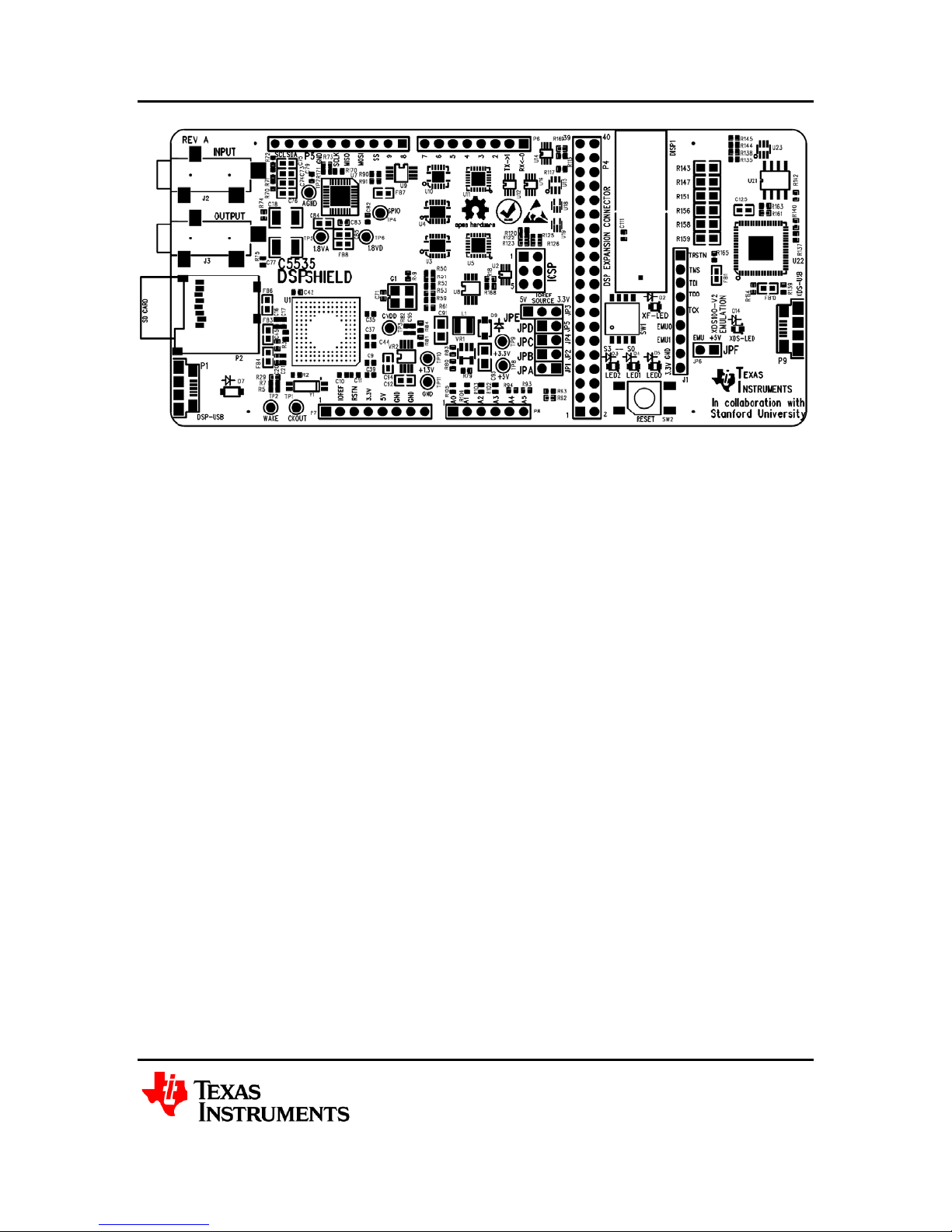
1.1 Key Features
The key features of the C5535 DSPShield are shown in Figure 1. The features include:
TI TMS320C5535AZHHA10 (100MHz) Digital Signal Processor
TI TLV320AIC3204IRGBR Stereo Audio Codec with separate stereo in and
stereo out connectors
Micro SD Card Connector
USB 2.0 interface to the C5535 DSP
OLED 96x16 pixel display
Arduino Compatible Header Connectors
Arduino Interface is compatible with Energia software IDE and API
Embedded USB XDS100-V2 JTAG emulator with secondary serial port
o JTAG is compatible with TI Code Composer Studio software IDE
o Secondary serial port is compatible with Energia software IDE and API
40-pin DSP Expansion Connector
3 user controlled LEDs,
4 user readable DIP switches
1 hardware reset push button switch
Flexible Power Sourcing
In Collaboration with Stanford University
page 1
Page 7
C5535 DSPShield H/W Reference Manual Version 0.1
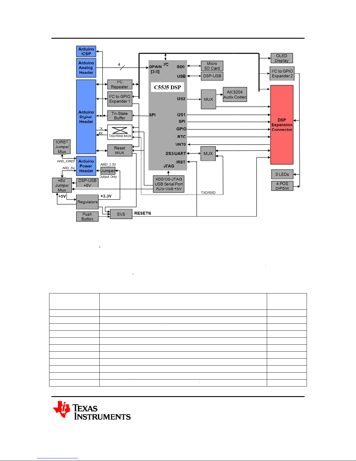
Figure 1. Key Features of the C5535 DSPShield
1.2 DSPShield Architecture
The C5535 DSP is a peripheral rich processor. However, to limit the pin count, the
C5535’s pins are heavily multiplexed. Depending on the application, the C5535 is
programmed with the appropriate internal peripherals routed to its external pins. The
DSPShield maintains this flexibility by using additional discrete multiplexers to connect
the C5535’s GPIO/peripheral pins to the appropriate points on the board. Additonal
flexibility can also be found in the power management for the board and in the
Arduino/DSPShield interface. The DSPShield block diagram is shown in Figure 2.
The DSPShield architecture consists of the following major blocks:
1. Power Management
2. The C5535 DSP and Internal Peripherals
3. DSPShield Peripherals
4. Arduino Interface
5. DSP Expansion Connector
6. XDS100-V2 Embedded Emulator
In Collaboration with Stanford University
page 2
Page 8
r
u
b
d
a
i
m
o
s
h
a
b
3
d
a
o
o
w
B
a
a
E
i
i
w
a
m
/
o
h
e
n
o
N
n
n
o
M
S
a
r
o
t
n
I
n
a
y
u
t
d
n
1
e
C55
5 DSPShield H
W Reference
anual
Version 0.
Figu
1.3
The
oar
in T
posit
User
Ele
SW1
SW2
P1
P2
P3/DI
P4
P5
P6
P7
P8
P9
e 2. C5535
User C
ser control
are throug
ble 1, with
ons on the
Control
ent
SP1
DSPShiel
ntrol Ele
the DSPSh
various he
reference t
oard are sh
Function
Quad DIP S
Reset Push
DSP-USB M
Micro SD C
OLED Displ
40-Pin DSP
Arduino Dig
Arduino Dig
Arduino Po
Arduino An
XDS-USB E
Block Dia
ments
ield throug
ders, conn
the sectio
wn in the t
itch for GPI
utton
icro USB Con
rd Adapter
xpansion Co
tal Header 1
tal Header 2
er Header
log Header
ulation Micr
In Collab
ram
jumpers an
ctors, and j
where thei
p and bott
ector
nector
USB connec
ration with
d switches.
cks. For co
functions
m assembl
tor
tanford U
nput and O
venience,
re describe
drawings i
iversity
tput to the
hey are list
. Their
Section 8.
Section
Descriptio
4.5
4.5
3.5
43.6, 4.4
4.2
4.6
6.1
6.1
6.1
6.1
5
page 3
d
n
Page 9
C5535 DSPShield H/W Reference Manual Version 0.1
P10 Arduino ICSP Male/Female Header 6.1
J1 Alternate JTAG Header when Embedded Emulator N/A 5.1
J2 Audio Codec MIC input 4.3
J3 Audio Codec Headphone output 4.3
JPA DSP-USB and/or XDS-USB +5V Input Select Jumper 2.1
JPB Arduino +5V Input/Output Select Jumper 2.1
JPC Arduino +3.3V Output ONLY Select Jumper 2.1
JPD Arduino IOREF Input/Output Select Jumper 6.1.1
JPE Internally generated Ardino IOREF +5V or +3.3V Select Jumper 6.1.1
JPF XDS-USB +5V Connector Select Jumper 5.2
LED-XF C5535 XF Status 3.3, 4.5
LED0 General Purpose LED 4.5
LED1 General Purpose LED 4.5
LED2 General Purpose LED 4.5
XDS-LED Emulator Connected Status 5.1
Table 1. User Control Elements
1.4 DSPShield Application Photos
Inset photographs here.
DSPShield + Arduino UNO
DSPShield + Arduino UNO + Arduino Shield (suggestions?)
DSPShield + Arduino Leonardo using 2 USB cables
DSPShield + DSP Daughter Card (Audio Shield)
DSPShield + Arduino Shield + DSP Daughter Card
Other???
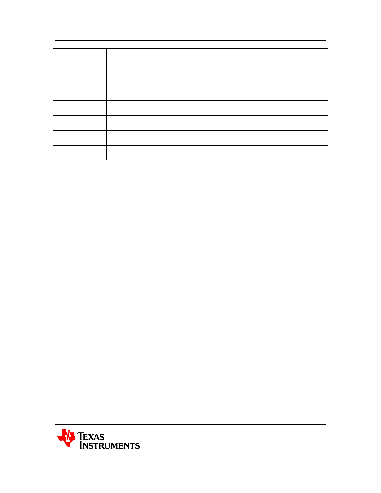
2 Power Management
The DSPShield requires a single +5V source. All other required voltages used on the
board are derived from this source.
2.1 External Power Interface
The +5V source can come from the DSP-USB connector (P1), XDS-USB connector (P9),
or from the Arduino Power Header (P7). The DSPShield power management block
diagram is shown in Figure 3. Jumpers JPA, JPB, JPC and JPF control the multiplexing
of power sources into and out of the board. Some common power management
configurations are listed in Table 2.
NOTES:
1. Schottky diodes allow both USB cables to be connected at the same time.
However, the inclusion of the diodes in the power path drops the nominal +5V to
about +4.3V due to the diode voltage drop.
2. The DSPShield does not use the +3.3V from the Arduino Power Header.
However, the DSPShield can source it.
In Collaboration with Stanford University
page 4
Page 10
r
S
h
n
h
h
h
n
h
h
n
h
R
V
n
h
e
d
d
A
d
A
O
r
i
d
3
r
x
S
S
S
b
S
b
e
s
o
/
o
e
P
+
J
O(Un
U
N
U
N
U
N
U
N
e
y
o
l
M
S
A
H
I
U
U
H
O
H
O
n
e
n
w
n
S
S
o
b
C
n
i
l
d
d
1
B
D
D
i
Figu
DSP
DSPS
Ardui
DSPS
DSPS
DSPS
Ardui
DSPS
DSPS
Ardui
DSPS
e 3. DSPS
hield Pow
ield Powered
o Power Hea
ield powered
ield powered
ield powered
o Power Hea
ield (Standield powered
o Power Hea
ield (Stand-
C55
ield Powe
r Multiple
from
er.
from DSP-U
from XDS-U
from DSP-U
er is sourced
lone Mode)
from XDS-U
er is sourced
lone Mode)
5 DSPShield H
Managem
ing
B
B
B.
y
B.
y
DS
SH
(I
SH
(I
SH
(I
SH
(I
W Reference
nt Block D
-USB
5V
PA
PEN
used)
NTED
PUT) (
NTED
PUT) (
NTED
PUT)
NTED
PUT)
anual
iagram
rduino
+5V
JPB
UNTED
S
INPUT)
(
OPEN
nused)
OPEN
nused)
UNTED
S
(
UTPUT)
UNTED
S
(
UTPUT)
Arduino
3.3V
JPC
OPEN
(Unused)
OPEN
(Unused)
OPEN
(Unused)
HUNTED
(OUTPUT)
HUNTED
(OUTPUT)
Version 0.
XDS-US
+5V
JPF
OPEN
(Unused)
OPEN
(Unused)
SHUNTE
(INPUT)
OPEN
(Unused)
SHUNTE
(INPUT)
Tabl
e 2. Input/
utput Pow
WA
valid
appli
+3.3
inter
NING: Ca
jumper sett
cation. One
pin on the
ally derive
e should b
ngs. Other
example of
Arduino P
+3.3V and
er Multiple
taken to pr
ettings ma
an invalid c
wer Header
the externa
In Collab
xing Optio
vent power
be possibl
nfiguratio
is being po
+3.3V will
ration with
s
.
sourcing c
, but must
is when JP
ered exter
be in confl
tanford U
nflicts. Tab
e evaluated
is shunte
ally by Ar
ct.
iversity
e 2 shows
for a specif
, and the
uino. The
page 5
c
Page 11
C5535 DSPShield H/W Reference Manual Version 0.1
2.2 Internal Voltages
There are a number of voltages that can be found on the DSPShield. They are derived
from various ICs and can be monitored at certain points. Table 3 lists the voltages, test
points and the devices/functions powered by the voltages.
Voltage Test Point Source Device/Functions
+5V TP8 External 1. LMR10510X DC-DC Regulator
2. ARD_INTF_VCC
3. ARD_5V (sourcing)
+3.3V TP9 LMR10510X DC-
DC Regulator (VR1)
+1.8V TP5, TP6 Internal AIC3204
LDO
+1.3V TP10 LP3982 LDO (VR2) 1. C5535 CVDDRTC
+1.3V
(C5535)
+1.3V
(C5535)
+1.3V
(C5535)
+1.8V
(FT2232H)
+7.3V Pint 1 of C70 Internal OLED DC-
GND TP11 - 1. Digital Ground
AGND0 TP7 - 1. AIC3204 Analog Ground
Pin 1 of C19
Or TP3
Pin 1 of C45 C5535 USB_LDOO 1. C5535 USB_VDDA1P3
Pin 1 of C53 C5535 ANA_LDOO 1. C5535 VDDA_ANA
Pin 1 of C125 FTDI FT2232H
C5535 DSP_LDOO 1. C5535 CVDD (0 OHM resistor mux
VREGOUT
DC regulator
Table 3. DSPShield Voltages and Grounds
1. C5535 USB_VDDOSC
2. C5535 USB_VDDA3P3
3. C5535 USB_VDDPLL
4. C5535 DVD_DRTC
5. C5535 LDOI
6. C5535 DVDDIO
7. All Muxes
8. SD Card
9. GPIO Expander 2
10. AIC3204 IOVDD
11. ARD_INTF_VCC
12. ARD_3.3V (sourcing)
13. DSP Expansion Header +3.3V
14. Emulator +3.3V
1. AIC3204 AVDD, TP5
2. AIC3204 DVDD, TP6
2. C5535 CVDD (0 OHM resistor mux
selectable)
3. GPAIN CLAMP DIODES
selectable. DEFAULT configuration)
2. C5535 USB_VDD1P3
2. C5535 VDDA_PLL
1. FT2232H VCORE
1. OLED Display
2.3 Voltage Monitoring
The output voltages of the LMR10510X DC-DC (+3.3V) regulator and the LP3982
(+1.3V) LDO regulator are monitored by a TPS386596L33 Quad Reset Supervisory IC.
In Collaboration with Stanford University
page 6
Page 12
C5535 DSPShield H/W Reference Manual Version 0.1
If either voltage drops below certain thresholds, the TPS65001’s active low open-drain
reset output will go low and reset the C5535 DSP and the DSPShield.
2.4 C5535 DSP Core Voltage
The C5535 DSP’s +1.3V Core Voltage, CVDD, can be driven either by its internal LDO
or by the LP3982 LDO. The selection is accomplished by populating certain
combinations of resistors R25, R26, R27 and R28. The two options are listed in Table 5.
CVDD = C5535 DSP_LDOO
(DEFAULT )
CVDD = LP3882 LDO
Table 4. C5535 DSP Core Voltage Selection
R25 = DNI
R26 = 0 Ohm Resistor
R27 = 0 Ohm 1/8W Resistor
R28 = DNI
R25 = 10.0K Ohm Resistor
R26 = DNI
R27 = DNI
R28 = 0.0 Ohm 1/8W Resistor
3 C5535 DSP and Internal Peripherals
The C5535 DSP is a high-performance, low-power, fixed-point Digital Signal Processor.
It has dual multipliers, dual ALUs, and a tightly coupled FFT hardware accelerator for
performing math intensive signal processing algorithms. It has a multiple I/O peripherals
that allow it to easily connect to serial Analog to Digital Converters, Digital to Analog
Converters and integrated codecs.
3.1 Parallel and Serial Peripherals
The C5535 DSP’s internal External Bus Selection Register (EBSR) determines which of
the following: LCD controller, I2S0, I2S1, I2S2, I2S3, UART, SPI, MMC/SD and GPIO
signals appear at the chip’s multiplexed GPIO pins. These peripherals can be grouped
into 3 groups as shown in Tables 5a, 5b and 5c. For each group, only one mode of
operation is available at a given time. Note that the DSPShield architecture further limits
the group mode selection.
PP MODE Multiplexed I/O Board Level limitations
Modes
0,2,3,4,5
Mode 1
-
SPI/I2S2/UART/6 GPIO Fully Supported.
In Collaboration with Stanford University
Not Supported
- I2S2 multiplexed between AIC3204 and DSP
Expansion Connector.
- UART multiplexed between Arduino, XDS
Serial Port and DSP Expansion connector.
- SPI multiplexed between Arduino and DSP
page 7
Page 13
C5535 DSPShield H/W Reference Manual Version 0.1
Expansion connector.
- GPIO[12:15] routed directly to DSP
Expansion connector.
- GPIO16 routed to the DSP Expansion
Connector IF R67 is Installed and R66 is Not
Installed (This is not the Default)
- GPIO17 routed to the DSP Expansion
Connector IF R69 is Installed and R68 is Not
Installed (This is not the Default)
Mode 6
SPI/I2S2/I2S3/6 GPIO Fully Supported.
- I2S2 multiplexed between AIC3204 and DSP
Expansion Connector.
- I2S3 routed to DSP Expansion Connector
when UART_MUX_SEL=0.
- SPI multiplexed between Arduino and DSP
Expansion connector.
- GPIO[12:15] routed directly to DSP
Expansion connector.
- GPIO16 routed to the DSP Expansion
Connector IF R67 is Installed and R66 is Not
Installed (This is not the Default)
- GPIO17 routed to the DSP Expansion
Connector IF R69 is Installed and R68 is Not
Installed (This is not the Default)
Table 5a. C5535 PPMODE
SP1
Multiplexed I/O Board Level limitations
MODE
Mode 0,1,2
SD1/I2S1/GPIO[6:11] Fully Supported.
- All signals are routed directly to the DSP
Expansion Connector.
Table 5b. C5535 SP1MODE
SP0
Multiplexed I/O Board Level limitations
MODE
Mode 0 SD0 SD0 signals are dedicated to the SD Card Connector
Modes 1, 2
-
Not Supported
Table 5c. C5535 SP0MODE
3.2 Clock Sources
The C5535 DSP has 3 input clock sources: USB_MXI pin, CLKIN pin, and an internal
Real Time Clock (RTC). The USB_MXI input is connected to a 12 MHz oscillator and is
the clock source for all USB peripheral activity. The CLKIN input is also connected to a
12 MHz oscillator while the RTC is connected to a 32.768 KHz crystal. Either CLKIN or
In Collaboration with Stanford University
page 8
Page 14
C5535 DSPShield H/W Reference Manual Version 0.1
the RTC can be the reference source for the C5535 DSP’s system clock generator.
Resistors R8, R9, R10 and R59 select the source as shown in Table 6. The different
clocks within the system clock generator block can be output on the C5535 DSP’s
CLKOUT pin and monitored at Test Point TP1.
System Clock Generator
Resistor Select
Reference Source
12MHz External Oscillator
(Default)
32.768 RTC R8=0 Ohm, R9=DNI, R10=0 Ohm, R59=DNI
R8=DNI, R9=10K Ohm, R10=DNI, R59=0 Ohm
Table 6. System Clock Generator Reference Source Select
3.3 ROM Bootloader
The C5535 DSP has an on-chip ROM Bootloader (RBL). It samples the following
interfaces, in order, looking for a boot signature: SPI EEPROM, I2C EEPROM,
MMC/SD0 AND UART/USB. Once a boot signature is detected, the C5535 DSP will
download the boot image and then jump to the entry point specified in the image. For the
DSPShield, the SD0 peripheral connected to the micro SD Card connector is the default
boot source. Figure 4 shows the Bootloader Software Architecture (from the C5535 DSP
datasheet). In the case where no boot source is found, the LED_XF will remain lit.
Figure 4. Bootloader Software Architecture
In Collaboration with Stanford University
page 9
Page 15
C
t
C
u
C
C
C
e
C
S
m
l
i
gur
I
p
N
p
n
a
D
c
r
r
r
h
3
u
u
t
p
n
U
o
b
o
a
e
/
o
P
t
t
a
e
o
h
a
c
t
a
u
6
o
M
S
E
a
A
r
i
d
c
C
a
e
s
n
C
E
w
t
T
-
s
g
,
e
t
n
C
o
e
l
e
O
t
s
1
u
e
3.4
The
resis
or.
The
outp
The
The
3.5
The
that i
s compliant
conn
/INT1, /I
5535 DSP’
5535 DSP’
ts. The out
5535 DSP’
5535 DSP’
USB Co
5535 DSP
ctor, P1, h
C55
T0, XF,
s /INT0 inp
s /INT1 inp
uts of the 2
s XF outpu
s Wakeup
troller
USB contro
with the U
s a micro-
5 DSPShield H
WAKEU
t is routed
t is connec
Expanders
controls th
in can be m
ller allows t
iversal Seri
SB form fa
W Reference
o the DSP
ed to the I2
re open-dr
LED, D2.
nitored on
e DSP to c
l Bus Spec
tor.
anual
xpansion
C to GPIO
in and are
logic “1”
Test Point
eate a high
fication ver
onnector. It
xpander I
ire-ORed t
turns on the
P2.
speed USB
ion 2.0. Th
Version 0.
has a pull
s’ /INT
gether.
LED.
slave devic
DSP-USB
p
3.6
The
and
the
Boot
mult
Fi
3.7
The
com
MMC/S
5535 DSP
D1. Interfa
icro SD ca
oader. Inte
plexed pins
e 5. Micro
I2C
2C periphe
liant with t
x Contr
has two em
e SD0 is c
d is the def
face SD1 is
MMC1/I2S
SD Card P
al provides
e Philips S
ller
edded Mul
nnected to
ult boot so
routed to th
1/GPIO[11:
eripheral
an interface
miconduct
imedia Car
micro SD
rce for the
DSP Exp
].
between th
rs I2C-bus
/Secure Di
ard adapter
5535 DSP’
nsion Conn
DSP and o
pecificatio
ital Contro
P2. For th
s on-chip R
ctor as par
ther device
(version 2.
lers, SD0
DSPShield
M
of the
that are
1). The
,
In Collab
ration with
tanford U
iversity
page 10
Page 16

C5535 DSPShield H/W Reference Manual Version 0.1
devices on the I2C bus on the DSPShield are listed in Table 7 along with their 7-bit
address.
I2C Peripheral I2C Address
GPIO Expander 1 0x20
GPIO Expander 2 0x21
OLED Display 0x3C
AIC3204 Codec 0x18
DSP Expansion Connector I2C Extension, +3.3V Logic Levels
Arduino Digital Interface I2C Extension, Buffered at +5V Logic Levels
DSP_I2C_EN must be a logic ”1”
Table 7. Devices on the I2C Bus
The I2C bus is also extended to the Arduino and DSP Expansion Connectors. For the
DSP Expansion Connector, the bus remains at +3.3V levels and is not buffered. For the
Arduino connector, the I2C bus is buffered by a TI PCA9515B I2C Repeater IC. The IC
provides a translation between the Arduino’s +5V logic levels and the C5535 DSP’s
+3.3V logic levels. On power up and reset, the PCA9515B is disabled. This isolates the
DSPShield’s internal I2C bus during the boot sequence. After boot, the C5535 DSP can
enable the PCA9515B by setting DSP_I2C_EN on Port0.2 of GPIO Expander 2 to a “1”.
4 DSPShield Peripherals
In addition to the C5535 DSP’s internal peripherals, the DSPShield has several external
peripherals that increase its functionality. The peripherals are:
1. Two TCA6416A 16-bit I2C to GPIO Expander chips
2. OLED display
3. TLV320ACI3204 Stereo Audio Codec
4. Micro SD Card connector
5. DIP Switch Inputs, LEDs, and Push Button Reset
6. Additional peripherals can be added through the use of the 40-pin DSP Expansion
Connector and the Arduino Interface Connectors.
4.1 I2C GPIO Expander
The two TCA6416A (I2C to GPIO) Expander chips increase the number of GPIOs under
the C5535 DSP’s direct control. Each chip provides an additional 16 GPIOs. Tables 8a
and 8b list the direction (after programming) and function of each GPIO.
On power up and reset, all the GPIOs are initialized as inputs. Some GPIO pins have
external pull up or pull down resistors connected to them that allow the various
DSPShield external peripherals to power up in a known state. For example, the U3 4-bit
1to2 multiplexer’s select pin is connected to Expander 2’s Port0.4 GPIO and also to a
In Collaboration with Stanford University
page 11
Page 17
C5535 DSPShield H/W Reference Manual Version 0.1
pull up resistor. On power up and reset the C5535 DSP’s I2S lines are multiplexed to the
codec.
To prevent glitches during initialization, the following sequence should be followed to
program output pins.
1. Program the Expander Output Port Registers to the default values listed in tables
8a and 8b.
2. Program the appropriate direction bit in the Expander Configuration Registers for
GPIOs that will be outputs.
3. After initialization, the Output Port Registers can be changed depending on the
application.
The GPIO Expanders also have an open drain active-low interrupt output. The interrupt
outputs of the two GPIO Expanders are wire-ORed together and connected to the C5535
DSP’s INT1N input. An interrupt is generated by any rising or falling edge of the port
inputs in the input mode. Resetting the interrupt is achieved when the data on the port is
changed to the original setting or when data is read from the port that generated the
interrupt. This interrupt feature of the GPIO Expander is very basic and lacks an interrupt
mask capability.
NOTES:
1. There are no external pull up or pull down resistors on GPIO pins that can be
programmed as input or output. If unconnected, these unused GPIO should be
programmed as an output to avoid floating inputs. The output value is irrelevant,
but a logic zero is preferred.
2. Expander 1 GPIOs can use +5V or +3.3V logic levels depending on the state of
JPD and JPE. Expander 2 GPIOs use +3.3V logic levels only.
Expander 1
I2CAddr=0x20
Port0.0 I/O Arduino I/O0
Port0.1 I/O Arduino I/O1
Port0.2 I/O Arduino I/O2
Port0.3 I/O Arduino I/O3
Port0.4 I/O Arduino I/O4
Port0.5 I/O Arduino I/O5
Port0.6 I/O Arduino I/O6
Port0.7 I/O Arduino I/O7
Programmed
Direction
In Collaboration with Stanford University
Function
Reset value: all GPIO are Inputs
- If unconnected, set to output a logic 0
- If unconnected, set to output a logic 0
- If unconnected, set to output a logic 0
- If unconnected, set to output a logic 0
- If unconnected, set to output a logic 0
- If unconnected, set to output a logic 0
- If unconnected, set to output a logic 0
page 12
Page 18

C5535 DSPShield H/W Reference Manual Version 0.1
- If unconnected, set to output a logic 0
Port1.0 I/O Arduino I/O8
- If unconnected, set to output a logic 0
Port1.1 I/O Arduino I/O9
- If unconnected, set to output a logic 0
Port1.2 O
Pull Down
Resistor on Pin
Port1.3 O
Pull Up
Resistor on Pin
Port1.4 O
Pull Down
Resistor on Pin
Port1.5 O
Pull Up
Resistor on Pin
Port1.6 O
Pull Down
Resistor on Pin
Port1.7 O
Pull Down
Resistor on Pin
UART_CNTRL0: Arduino UART Mux Control
Default = 0
UART_CNTRL1: Arduino UART Mux Control
Default = 1
UART_CNTRL2: Arduino UART Mux Control
Default = 0
UART_CNTRL3: Arduino UART Mux Control
Default = 1
RST_CNTRL0: Reset Mux Control
Default = 0
RST_CNTRL1: Reset Mux Control
Default = 0
Table 8a. Expander 1 GPIO Definitions
Expander 2
I2CAddr=0x21
Port0.0 O LED0: 0=OFF, 1=ON
Port0.1 O LED1: 0=OFF, 1=ON
Port0.2 O
Port0.3 O
Port0.4 O
Port0.5
Programmed
Direction
Pull Down
Resistor on Pin
Pull Down
Resistor on Pin
Pull Up
Resistor on Pin
O
Pull Up
Resistor on Pin
Function
Reset value: all GPIO are Inputs
DSP_I2C_EN
0= Disable, 1= Enable
Default = 0
SPI_RX_SEL
0=SPI RX input from Arduino MISO
1=SPI RX input from DSP Expansion Header
NOTE: Manufacturing Default = 0. An alternative pull up
resistor pad is available on the board.
I2S2_MUX_SEL
0=Connected to DSP Expansion Header
1=Connected to AIC3206 Codec
NOTE: Manufacturing Default = 1. An alternative pull down
resistor pad is available on the board.
UART_MUX_SEL
0=Connected to DSP Expansion Header
1=C5535 DSP UART TX and RX connected to Arduino
UART multiplexing circuitry
NOTE: Manufacturing Default = 1. An alternative pull down
resistor pad is available on the board.
In Collaboration with Stanford University
page 13
Page 19

C5535 DSPShield H/W Reference Manual Version 0.1
Port0.6 O LED2: 0=OFF, 1=ON
Port0.7 O
Pull Down
Resistor on Pin
Port1.0 I/O DSP Expansion Header PIN6
Port1.1 I/O DSP Expansion Header PIN4
Port1.2 I/O DSP Expansion Header PIN5
Port1.3 I/O DSP Expansion Header PIN3
Port1.4 I State of switch 4 on DIP Switch SW1
Port1.5 I State of switch 3 on DIP Switch SW1
Port1.6 I State of switch 2 on DIP Switch SW1
Port1.7 I State of switch 1 on DIP Switch SW1
DSP_SPI_EN
0=Arduino SPI TXB0104 Transceiver Disabled
1=Arduino SPI TXB0104 Transceiver Enabled
Default = 0
- If unconnected, set to output a logic 0
- If unconnected, set to output a logic 0
- If unconnected, set to output a logic 0
- If unconnected, set to output a logic 0
Table 8b. Expander 2 GPIO Definitions
4.2 OLED Display
The OLED Display provides a 96x16 pixel display. It is programmed via the C5535
DSP’s I2C bus and has an I2C address of 0x3C.
4.3 TLV320ACI3204 Audio Codec
The AIC3204 Audio Codec interfaces to the C5535 DSP via the I2C and I2S2 buses. The
C5535 DSP’s I2S2 Bus is routed to the AIC3204 when I2S2_MUX_SEL = 1. The
AIC3204’s I2C address is 0x18.
The microphone stereo input is routed to the Pink jack, J1. The head phone stereo output
is routed to the Green jack, J2.
4.4 Micro SD Card Connector
Interface SD0 is connected to a micro SD card connector, P2. The micro SD card is the
default boot source for the C5535 DSP’s on-chip ROM Bootloader (RBL).
4.5 DIP Switch Inputs, LEDs and Push Button Reset
The status of switches 1, 2, 3 and 4 of DIP switch SW1, can be read by the C5535 DSP
via Port1.7, 1.6, 1.5, 1.4 of the GPIO Expander 2, respectively. “ON” corresponds to a
logic “1” in the GPIO Expander Input Register.
Three general purpose status LEDs are available for display by the C5535 DSP. They are
controlled by the output value of Port0.0, 0.1, and 0.6 of GPIO Expander 2. They
correspond to LEDs labeled as LED0, LED1 and LED2 on the board. A separate LED is
In Collaboration with Stanford University
page 14
Page 20

C5535 DSPShield H/W Reference Manual Version 0.1
tied to the C5535 DSP’s XF general purpose output pin. It is labeled LED-XF on the
board. Writing a logic “1” to the appropriate registers will turn on the LEDs.
A manual reset is provided by push button SW2. Pressing this switch will place the
DSPShield in its default state.
4.6 DSP Expansion Connector
The DSP Expansion Connector routes power, ground, and various C5535 DSP GPIOs
and signals to a 40-pin Female Receptacle, P2. The receptacle mates to standard 0.1”
pitch 0.025” square post male headers. The signals available on the DSP Expansion
Connector are listed in Table 9. All signals used 3.3V logic levels.
Pin Signal Name Direction Function
1 +5V O Power to Header
2 +3.3V O Power to Header
3 X_GPIO3V3_13 I/O GPIO (Expander2 Port1.3)
4 X_GPIO3V3_11 I/O GPIO (Expander2 Port1.1)
5 X_GPIO3V3_12 I/O GPIO (Expander2 Port1.2)
6 X_GPIO3V3_10 I/O GPIO (Expander2 Port1.0)
7 X_SCL O I2C SCL
8 X_LCD_D9_I2S2_FS_GP19_SPI_CS0 I/O C5535 PPMODE SIGNALS
9 X_SDA O I2C SDA
10 X_LCD_D8_I2S2_CLK_GP18_SPI_CLK I/O C5535 PPMODE SIGNALS
11 X_NMIN I/O C5535 INT0
12 X_LCD_D11_I2S2_DX_GP27_SPI_TX I/O C5535 PPMODE SIGNALS
13 X_RESETN I/O C5535 PPMODE SIGNALS
14 X_LCD_D10_I2S2_RX_GP20_SPI_RX I/O C5535 PPMODE SIGNALS
15 GND - GROUND
16 X_LCD_D2_GP12 I/O C5535 PPMODE SIGNALS
17 X_DSP_SPI_TX I/O C5535 PPMODE SIGNALS
18 X_LCD_D3_GP13 I/O C5535 PPMODE SIGNALS
19 X_SPI_RX I/O C5535 PPMODE SIGNALS
20 X_LCD_D4_GP14 I/O C5535 PPMODE SIGNALS
21 X_DSP_SPI_CS3 I/O C5535 PPMODE SIGNALS
22 X_LCD_D5_GP15 I/O C5535 PPMODE SIGNALS
23 X_DSP_SPI_CS2 I/O C5535 PPMODE SIGNALS
24 X_RTCCLK_GP16 I/O R66=IN, R67=DNI (DEFAULT)
DSP_RTC_CLKOUT
R66=DNI, R67=IN
X_LCD_D6_GP16
25 X_DSP_SPI_CS1 I/O C5535 PPMODE SIGNALS
26 X_12MHZ_GP17 I/O R68=IN, R69=DNI (DEFAULT)
DSP_EXP_12MHZ (OSC)
R68=DNI, R69=IN
X_LCD_D7_GP17
In Collaboration with Stanford University
page 15
Page 21

E
D
a
n
e
o
p
h
_
C
_
C
2
D
3
D
4
D
5
D
x
o
n
C
r
e
e
T
e
3
K
_
_
G
_
G
D
D
o
u
D
n
t
u
n
m
/
o
_
C
_
F
_
_
g
e
t
t
b
o
h
M
S
III
I
I
IS I
I
I
I
I
I
t
V
s
n
t
t
b
e
2
n
O
O
o
2
e
e
e
S
S
E
S
E
S
E
S
E
S
E
S
E
p
S
s
b
c
T
1
26
28
29
30
31
32
33
34
35
36
37
38
39
40
Tabl
X_DSP_SPI
X_MMC1_
X_DSP_SPI
X_MMC1_
X_LCD_D1
X_MMC1_
X_LCD_D1
X_MMC1_
X_LCD_D1
X_MMC1_
X_LCD_D1
X_MMC1_
GND
GND
e 9. DSP E
C55
CS0
LK_I2S1_CL
CLK
MD_I2S1_FS
_UART_RTS
0_I2S1_DX_
_UART_CTS
1_I2S1_RX_
_UART_RX
2_GP10
_UART_TX
3_GP11
pansion C
5 DSPShield H
_GP6
GP7
GP28_I2S3_
P8
GP28_I2S3_
P9
_GP28_I2S3
_GP31_I2S3
nnector Si
W Reference
LK
RX
DX
nal Defini
anual
/O C55
/O C55
/O C55
/O C55
/O C55
/O C55
/O C55
/O C55
/O C55
/O C55
/O C55
/O C55
- GR
- GR
ions
35 PPMODE
35 SP1MOD
35 PPMODE
35 SP1MOD
35 PPMODE
35 SP1MOD
35 PPMODE
35 SP1MOD
35 PPMODE
35 SP1MOD
35 PPMODE
35 SP1MOD
UND
UND
Version 0.
IGNALS
SIGNALS
IGNALS
SIGNALS
IGNALS
SIGNALS
IGNALS
SIGNALS
IGNALS
SIGNALS
IGNALS
SIGNALS
5
The
the l
Con
If th
with
snap
popu
XDS
560.
5.1
The
This
is shown in
mulati
SPShield i
test Code
ection is th
embedded
ut the emul
ed into two
ating Head
FTDI F
eart of the
n
corporates
omposer St
ough the X
mulator is
ation circui
pieces. Em
r J1 and co
2232H
mbedded e
Figure 6.
an embedd
dio (CCS)
S_USB mi
ot required
ry. The prin
lation capa
necting it t
ulator is t
d XDS100-
hat support
cro USB co
or desired,
ed circuit b
ility can b
an externa
e FTDI FT
2 Emulat
the TMS3
nector.
he DSPShi
oard is scor
restored to
l TI JTAG
232H, a U
. It is com
0C5535 D
ld can be a
d so that it
a snapped
mulator su
B to UAR
atible with
P.
sembled
can be
oard by
h as the TI
/GPIO IC.
In Collab
ration with
tanford U
iversity
page 16
Page 22

C5535 DSPShield H/W Reference Manual Version 0.1
Figure 6. USB JTAG Emulation Based on the FTDI FT223H
The FT2232H has two channels. When connected to a PC with the appropriate software
drivers installed, one channel will enumerate as a TI XDS Emulator and the second
channel will enumerate as a generic USB serial port. Once the PC connection is
established, the XDS_LED will turn on.
The XDS100 channel is connected to the C5535 DSP’s JTAG inputs and the serial port
channel is connected to the C5535 DSP’s UART interface. The data signals, TXD/RXD,
and the flow control signals, RTS/CTS, are appropriately cross connected.
If not used for flow control, the FT2232H’s RTS pin can also be used as an external reset
source for the DSPShield (see Section 6.2). If RTS is being used for flow control, the
external reset can be driven by the FT223H’s DTR pin by removing R161 and installing a
0 Ohm resistor on R163. RTS is the default emulator reset source for the EmuResetSrc
signal.
On power up, RTS and DTR are tri-stated and a resistor pulls up the EmuResetSrc signal.
Since RTS and DTR are defined as active low signals, RTS and DTR will remain high
after USB enumeration. A PC can reset the DSPShield by toggling EmuResetSrc, (RTS
or DTR) signal High to Low to High.
5.2 Power via XDS-USB
It is possible to power the DSPShield via the XDS_USB connector. See section 2.1. The
FT2232H itself is powered by the +3.3V from VR1. It also has an internal Power-On
Reset that is independent from the DSPShield’s board level system reset.
6 Arduino Interface
The DSPShield has a standard Arduino Interface on connectors P5, P6, P7, P8 and P10.
The connectors are 0.1” pitch female receptacles with long 0.025”sq tails. The long tails
for P5, P6, P7, and P8 on the bottom side allow the DSPShield to stack on top of an
Arduino board and at the same time repeat the Arduino signals on the top side. The ICSP
connector, P10 is similar except that is mounted with the female receptacle on the bottom.
The Arduino connector signals are grouped by function and are defined in Tables 10a,
10b, 11c, 10d and 10e.
Pin Signal Name Direction Function
1 ARD_IO0 I/O
O
2 ARD_IO1 I/O
I
3 ARD_IO2 I/O I/O2
4 ARD_IO3 I/O I/O3
In Collaboration with Stanford University
I/O0
Alt: UART C5535 TXD Arduino
I/O1
Alt: UART C5535 RXD Arduino
page 17
Page 23

C5535 DSPShield H/W Reference Manual Version 0.1
5 ARD_IO4 I/O I/O4
6 ARD_IO5 I/O I/O5
7 ARD_IO6 I/O I/O6
8 ARD_IO7 I/O I/O7
Table 10a. Arduino Digital Header P6
Pin Signal Name Direction Function
1 ARD_IO8 I/O I/O8
2 ARD_IO9 I/O I/O9
3 ARD_SPI_SS I/O SPI Chip Select
4 ARD_MOSI I/O SPI MOSI
5 ARD_MISO I/O SPI MISO
6 ARD_SCK I/O SPI_SCK
7 GND - Ground
8 ARD_AREF - No Connection
9 ARD_SDA I/O I2C SDA
10 ARD_SCL I/O I2C SCL
Table 10b. Arduino Digital Header P5
Pin Signal Name Direction Function
1 ARD_MISO I/O SPI MISO
2 ARD_+5V I/O +5V, Can be Input or Output Source
3 ARD_SCK I/O SPI_SCK
4 ARD_MOSI I/O SPI MOSI
5 ARD_RESETN I/O Bidirectional Reset Pin
6 GND - Ground
Table 10c. Arduino ICSP Header P10
Pin Signal Name Direction Function
1 ARD_NC - No Connection
2 ARD_IOREF I/O Interface Logic Voltage
3 ARD_RESETN I/O Bidirectional Reset Pin
4 ARD_+3.3V O DSPShield does not use this voltage, but can
source it.
5 ARD_+5V I/O +5V, Can be Input or Output Source
6 GND - Ground
7 GND - Ground
8 ARD_VIN - No Connection
Table 10d. Arduino Power Header P7
Pin Signal Name Direction Function
1 ARD_AD0 I Analog Input to C5535 GPAIN0
NOTE: Max Signal Level is +1.3V
2 ARD_AD1 I Analog Input to C5535 GPAIN1
NOTE: Max Signal Level is +1.3V
3 ARD_AD2 I Analog Input to C5535 GPAIN2
NOTE: Max Signal Level is +1.3V
In Collaboration with Stanford University
page 18
Page 24

A
f
e
f
gur
1
D
b
d
b
r
i
S
S
u
o
P
s
s
n
c
s
a
v
o
3
e
e
O
A
e
L
e
J
c
/
o
f
n
A
r
a
g
a
h
E
M
S
a
O
I
4
4
I
3R93
c
P
t
I
l
n
C
gn
2
e
2
e
m
i
t
o
h
e
3
1
c
c
e
h
f
e
1
)
)
C
n
4
5
6
Tabl
6.1
The
Inter
activ
Inter
ARD_AD3
ARD_AD4_
ARD_AD5_
e 10e. Ard
Arduin
rduino/DS
ace consist
low Reset
ace consist
C55
DA
CL
ino Analog
/DSPShi
Shield Int
of 10 GPI
signal. The
of +5V, +3
5 DSPShield H
Header P8
ld Inter
rface Block
s, an I2C i
nalog Inte
.3V, GND,
W Reference
I An
N
/O R9
R9
/O R9
ace Blo
Diagram is
terface, a S
face consis
nd IOREF.
anual
log Input to
TE: Max Si
= Installed I
= Not Install
= Installed I
= Not install
k Diagra
shown in F
I interface
s of 4 anal
5535 GPAIN
al Level is +
C SDA
d, No Conne
C SDA
d, No Conne
gure 7. The
and a bi-dir
g inputs. T
Version 0.
.3V
tion (Default
tion (Default
Digital
ctional
e Power
Fi
6.1.
The
oar
e p
conf
e 7. Ardui
Interfa
SPShield i
s. The volt
ogrammed
gurations f
o Interfac
e Logic
compatibl
ge supply o
ia jumpers
r the interfa
Block Dia
evels
with +5V
f the DSPS
PD and JP
e buffer IC
In Collab
ram
nd +3.3V v
ield buffer
. Table 11
s.
ration with
ersions of t
Cs that inte
ists the diff
tanford U
e Arduino
rface to the
rent voltag
iversity
amily of u
Arduino ca
sourcing
page 19
Page 25
C5535 DSPShield H/W Reference Manual Version 0.1
Arduino Interface Voltage Sourcing
JPD JPE
Externally Sourced from Arduino Power Header IOREFF.
IOREF is an input.
Default
Internally Sourced +5V OPEN
Internally Sourced +3.3V OPEN
Stand-Alone Mode
Internally Sourced +5V. IOREF is an output.
Stand-Alone Mode
Internally Sourced +3.3V. IOREF is an output.
SHUNTED
(Unused)
(Unused)
SHUNTED
(INPUT)
SHUNTED
(INPUT)
OPEN
(Unused)
SHUNTED
[1-2]
SHUNTED
[2-3]
SHUNTED
[1-2]
SHUNTED
[2-3]
Table 11. Arduino Interface Voltage Source
6.1.2 Analog Inputs
Thee 4 inputs from the Analog Connector are routed to the C5535 DSP’s GPAIN[3:0]
inputs. The analog signal magnitude must be limited to 0 to +1.3V. For protection there
are 100K Ohm series resistors in the input path to limit the input current. They can be
replaced with a different value for specific applications. Additionally, there are Schottky
diodes for clamping the voltage swing to +1.3V and GND. However, it is recommended
to use an input buffer circuit that will limit the input voltage swing by design.
If the Arduino Analog Header is being used only in a pass through mode, it is
recommended that the input series resistors be removed. This disconnects the C5535 DSP
from the Arduino Analog Header and will allow the Arduino Analog pins to safely pass
signals up to 5 volts without damaging the C5535 DSP.
6.2 Arduino/DSPShield Reset Multiplexing
The ARD_RESETN pin on the Arduino Digital Header is the focal point of the
DSPShield’s multiplexing circuitry. The ARD_RESETN is treated as bi-directional
signal that can be controlled by either the Arduino or the C5535 DSP. The different Reset
Modes are illustrated in Figures 8a through 8f.
In Collaboration with Stanford University
page 20
Page 26

gur
m
a
r
r
n
g
e
e
3
e
m
t
l
/
o
u
b
g
r
M
S
l
o
2
l
n
T
u
h
u
u
u
1
r
e
C55
5 DSPShield H
W Reference
anual
Version 0.
Fi
The
Exp
up o
are p
circu
e 8. Ardui
ultiplexin
nder2. Som
when SW2
ogrammed,
try in the d
o/DSPShi
circuitry is
Common
is pressed,
the externa
fault state.
ld Reset M
controlled
ultiplexin
he GPIOs o
pull down
In Collab
ltiplexing
y the signa
configurati
f Expander
esistors wi
ration with
Circuitry
s RST_CN
ons are liste
are config
l maintain t
tanford U
RL[1:0] in
d in Table 1
red as inp
e Reset m
iversity
GPIO
2. On powe
ts. Until th
ltiplexing
page 21
y
Page 27

C5535 DSPShield H/W Reference Manual Version 0.1
ARD_
RESETN
0 X 0
X 0 0
X X 0 1
X X 1 0
X X 1 1
X 0 X X
X X X X
EmuRes
etSrc
RST_
CNTRL1
Expander2
Port1.7
Default
Default
RST_
CNTRL0
Expander2
Port1.6
0
Default
0
Default
Reset Modes
Arduino Resets DSPShield
A logic “0” from the ARD_RESETN pin will reset
the DSPShield.
Emulator Resets Arduino and DSPShield
A logic “0” from the EmuResetSrc will drive the
ARD_RESETN pin and reset Arduino and the
DSPShield.
Default resistor placement.
R122 = Installed, R119 = Not Installed
C5535 Self Reset (not normally used)
The C5535 drives a logic “0” onto the
ARD_RESETN pin.
The C5535 resets itself and DSPShield.
C5535 Isolated from ARD_RESETN
The C5535 cannot generate or receive an external
reset on the ARD_RESETN pin.
C5535 Resets Arduino
The C5535 drives a logic “0” onto the
ARD_RESETN pin.
The C5535’s own reset input is isolated from the
ARD_RESETN pin.
Emulator Resets DSPShield Only
R122 = Not Installed, R119 = Installed
Requires resistor placement modification
Push Button Reset
Pressing the pushbutton SW2 will reset the
DSPShield.
Table 12. Arduino/DSPShield Reset Multiplexing Control
6.2.1 Default Configuration
In the default configuration, the DSPShield is sensitive to the state of the ARD_RESETN
pin on the Arduino Digital Connector. Either the Arduino or the Emulator can reset the
C5535 and DSPShield by applying a logic “0” to the ARD_RESETN pin. See Figures 8a
and 8b.
In Collaboration with Stanford University
page 22
Page 28

C5535 DSPShield H/W Reference Manual Version 0.1
6.2.2 C5535 Isolated from ARD_RESETN pin
In this configuration, the DSPShield is disconnected from the ARD_RESETN pin. Only
the Emulator EmuResetSrc or the push button can reset the DSPShield. See Figure 8c
6.2.3 C5535 Resets Arduino
In this configuration, the DSPShield’s own reset input is isolated from the
ARD_RESETN pin. At the same time it drives a logic “0” onto the ARD_RESETN pin
and therefore resets the Arduino. See Figure 8d.
6.2.4 C5535 Self Resets
In this configuration, the C5535 generates a logic “0” that is routed to the
ARD_RESETN pin and also to the DSPShield’s reset circuitry. This is a “circular” reset
that will cause the C5535 to reboot. See Figure 8e.
6.2.5 Emulator Only Resets the DSPShield
There may be some application that requires that the emulator be able to reset the
DSPshield without resetting the Arduino. In this case, by switching R119 and R122, the
EmuResetSrc signal is isolated from the ARD_RESETN pin. See Figure 8f.
6.3 DSPShield UART Multiplexing
The C5535 DSP’s UART peripheral can be connected to the DSP Expansion Connector,
Arduino Digital Header IO0 and IO1 pins, or the XDS100 JTAG Serial Port. The
multiplexing of the UART signals are controlled by UART_MUX_SEL and
UART_CNTRL[3:0] via the GPIO Expanders. Table 13 lists the 4 multiplexing modes
used in most applications. The different UART Multiplexing Modes are illustrated in
Figure 9.
ARD_
UART_
CNTRL2
Expander1
Port1.4
UART_
MUX_
SEL
Expander2
Port0.5
0 1 0 1 0
1 1 0 1 0
1 0 0 0 0
ARD_
UART_
CNTRL3
Expander1
Port1.5
ARD_
UART_
CNTRL1
Expander1
Port1.3
ARD_
UART_
CNTRL0
Expander1
Port1.2
C5535 UART Connection Modes
DSP Expansion Connector Mode
C5535 UART DSP Expansion Header
ARD_IO[1:0]: No connection
XDS SerPort: No connection
Default Communications Mode
C5535 UART ARD_IO[1:0]
ARD_IO1: No connection
ARD_IO0 + XDS SerPort TxD C5535 RxD
XDS SerPort RxD C5535 TxD
Arduino Communication Mode
In Collaboration with Stanford University
page 23
Page 29

R
r
b
c
b
g
5
o
n
3
T
i
n
m
/
o
a
m
e
o
e
M
S
x
n
n
n
o
a
1
o
o
o
e
c
l
5
5
u
c
5
n
t
1
d
e
1
Tabl
WA
Othe
us
ein
X
e 13. C553
NING: Th
combinati
ontention o
enabled at
C55
0
DSP UAR
e Table13 li
ns are poss
the Ardui
the same ti
5 DSPShield H
1
Peripher
sts 4 valid
ble. Howev
o IO[1:0] c
e. Please r
W Reference
1
l Multiple
ultiplexing
r, some co
nnector pi
fer to the sc
anual
ARD_IO0
XDS SerP
ARD_IO1
XDS Seri
ARD_IO[
XDS SerP
XDS SerP
ing Contr
modes bas
trol signal
s due to mu
hematic.
C
rt RxD C
+ XDS SPort
l Port Comm
:0]: No conne
rt RxD C5
rt TxD C5
l
d on the 5 c
ombinatio
tiple tri-sta
Version 0.
535 TxD
535 TxD
C5535 RX
nication Mo
tion
535 TxD
35 RxD
ontrol signa
s may caus
e buffers
e
ls.
In Collab
ration with
tanford U
iversity
page 24
Page 30

r
1
R
R
a
O
e
g
2
a
i
nUNO
r
e
e
3
n
X
3
R
3
h
x
E
E
e
w
o
o
d
S
o
h
u
r
e
5
o
U
S
X
n
D
3
T
C
t
C
s
p
t
e
n
s
R
T
n
i
h
o
5
T
P
T
e
d
s
/
o
i
t
p
’
5
D
_
4
u
p
f
d
d
S
r
R
A
C
M
S
p
-
g
U
h
L
u
e
i
A
t
W
N
a
m
d
R
o
o
d
n
b
e
u
l
T
O
A
O
i
e
m
M
n
r
T
r
h
e
E
r
u
d
b
A
D
o
e
p
t
s
1
d
d
o
o
t
’
n
r
Figu
6.3.
UA
UA
Exp
nsion Conn
GPI
How
up re
sistor, R41,
chan
e 9. DSPS
DSP E
T_MUX_S
T_MUX_S
signals, de
ver, on po
ed by rem
C55
ield UAR
pansion
L controls
L = 0, the
ctor. In thi
ending on
er up and r
on the selec
ving R41 a
5 DSPShield H
Multiplex
onnecto
he select in
5535 DSP
case, the C
he PPMO
set, UART
t input of U
installing
W Reference
ng Modes
ut of the 4
s UART si
535 DSP
E value in t
MUX_SE
. The defa
R42 install
anual
it multipl
nals are ro
ART signa
e C5535 D
= 1 due to
lt for UAR
d with a 0
xer, U4. W
ted to the D
s can also b
SP’s ESBR
the presenc
_MUX_S
hm resisto
Version 0.
en
SP
e I2S3 or
register.
of the pull
L can be
.
6.3.
For
IO0
to an
dow
This
Afte
proc
TXD
rout
6.3.
Whe
the
C55
is O
C55
Arduin
generic Ar
s connected
onboard U
load code t
, the DSPS
is the Defa
both the A
ssors is pos
line is rout
d to the C5
Emulat
UART_M
DS JTAG
5 DSP’s T
’ed with o
5 DSP RX
IO[1:0]
uino, IO1 i
to the UA
B to UAR
the Ardui
ield can be
lt Commun
duino and t
sible by ch
d to the C5
35 DSP’s
Serial
X_SEL=0
erial Port.
D line. Wh
e of the Ar
line. Care
connected
T RXD inp
bridge chi
o UNO uC
programme
cations Mo
e C5535 D
osing the A
35 DSP’s
XD line. Se
ort
, the C5535
he XDS JT
n UART_
uino’s IO[1
hould be ta
In Collab
to the Ardu
t. For the
. The USB
rom a PC.
by the U
e. See Figu
P are oper
duino Com
XD line an
e Figure 8b.
DSP’s UA
G Serial P
NTRL0=0,
:0] connect
ken that Ar
ration with
no uC’s U
rduino UN
o UART br
hen stack
O’s USB to
re 8a
tional, com
unication
d the Ardui
T signals a
ort RXD lin
the XDS J
r pins befo
uino and th
tanford U
RT TXD o
, IO0 is als
idge chip is
d on top of
UART bri
unication
ode. The
o uC’s RX
e always c
e is tied dir
AG Serial
e being rou
e emulator
iversity
tput pin an
o connecte
used to
the Arduin
ge chip als
etween bo
rduino uC
line is
nnected to
ctly to the
ort TXD li
ed to the
erial port a
page 25
.
h
s
e
e
Page 31

C5535 DSPShield H/W Reference Manual Version 0.1
not transmitting at the same time. There is no electrical conflict, but the transmission will
be corrupted. See Figure 8a and 8b. When exclusive communication with the emulator
serial port is desired, UART_CNTRL0 should be set to a logic “1”. This shuts off the
Arduino’s TXD signal from reaching the C5535 DSP’s RXD input. See Figure 8c.
When a single chip uC based Arduino board such as the Arduino Leonardo is used, there
is no direct UART path between a PC and the DSPShield for C5535 code downloading.
In this case, the Emulator Serial Port can be used as an alternative for this purpose. Two
USB PC cables are required, one to the Arduino Leonardo and one to the DSPShield’s
XDS-USB micro USB connector.
6.4 Arduino/DSPShield I2C Interface
The C5535 DSP’s I2C bus is isolated from the Arduino I2C bus by a PCA9515B I2C
Repeater IC. The PCA9515B provides isolation and voltage level translation. The C5535
DSP side of the IC operates at +3.3V levels, while the Arduino side operates at voltages
levels determined by jumpers JPD and JPE.
The I2C specification allows multiple masters on the bus. When the PCA9515B is
enabled (ARD_I2C_EN = 1), the C5535 DSP can operate as a master and communicate
with the peripherals on board the DSPShield as well as any slaves on the Arduino side.
Conversely, an Arduino can be a master and communicate with any of the peripherals on
the DSPShield. For example, the Arduino master could make use of the DSPShield’s
OLED Display.
On power up and reset, ARD_I2C_EN = 0. This isolates the Arduino and C5535 DSP
I2C buses and allows the C5535 DSP to program the DSPShield’s on-board peripherals
without worrying about access conflicts with an Arduino Master.
6.5 Arduino SPI Interface
The Arduino SPI interface is available on both the Arduino Digital and ICSP connectors.
The Arduino uC SPI peripheral can operate in a master or slave mode while the C5535
DSP SPI peripheral can only operate in a master mode. The two SPI buses are connected
via a TXB0104 bidirectional voltage level translator buffer. The TXB0104 provides
automatic direction sensing as well as tri-state isolation capability. The control signals on
Expander 2 used to control the SPI interface multiplexing are listed in Table 13. The
different Multiplexing Modes are illustrated in Figure 10.
Expander2 Port0.7
DSP_SPI_EN
0 X Arduino uC SPI Bus Master and C5535 SPI
1 0 Arduino uC SPI Slave or SPI I/O tri-stated.
SPI_RX_SEL
Expander2 Port0.3
Arduino SPI Interface (P5 & P10)
Bus Isolated
C5535 SPI Bus Master
In Collaboration with Stanford University
page 26
Page 32

C
t
h
gur
1
n
r
b
e
a
D
n
S
o
u
o
n
S
t
e
3
e
I
o
d
i
C
M
o
/
o
l
s
r
x
t
P
e
r
t
r
M
S
C
T
a
n
d
e
s
t
D
n
o
e
n
m
e
d
s
e
n
t
W
o
o
1
d
n
s
Tabl
e 13. Ardui
The
direc
on t
e Digital C
5535 DSP
ly to the D
C55
o/DSPShi
has four SP
P Expansi
nnector an
5 DSPShield H
ld SPI Mu
chip select
n Connecto
the DSP E
W Reference
tiplexing
, CS[3:0].
. CS0 is sh
pansion Co
anual
- DSP_SP
connect
ontrol
he chip sel
red betwee
nector.
I_CS0 is rout
r pin
cts, CS[3:1
the Ardui
Version 0.
d to SS
], are route
o SPI SS pi
Fi
6.5.
Whe
cont
Reg
the
uff
e 10. Ard
Arduin
the Ardui
ol signal D
r disabled,
rdless of th
SP Expansi
ino/DSPSh
Master/
o is in SPI
P_SPI_EN
he Arduino
state of the
on Connect
eld SPI In
5535 DS
aster mod
in Expande
has full indi
TXB0104,
r. See Figu
In Collab
erface
Isolate
, the TXB0
2 should b
vidual acce
he C5535
e 10a.
ration with
104 buffer
programm
s to the Ar
SP SPI bu
tanford U
ust be tri-s
d to a “0”.
uino SPI c
is always c
iversity
ated. The
ith the
nnector pin
nnected to
page 27
.
Page 33

C5535 DSPShield H/W Reference Manual Version 0.1
6.5.2 Arduino Slave/C5535 DSP Master
This is a possible communication link between the Arduino and the C5535 DSP. In this
configuration, DSP_SPI_EN should be programmed to a “1” and SPI_RX_SEL should be
set to a “0”. The former turns on the TXB0104 buffer and the latter routes the Arduino
MISO pin on the connector to the C5535 DSP’s SPI RX input. The C5535 DSP’s SPI
Chip Select 0 (CS0) signal is routed to the Arduino SS chip select pin. See Figure 10b.
6.5.3 Arduino Isolated/C5535 DSP Master
This configuration allows the C5535 DSP to be the sole Master of the Arduino SPI
interface. DSP_SPI_EN should be programmed with a “1” and SPI_RX_SEL should be
programmed with a “0”. The Arudino uC SPI pins should be tri-stated either by keeping
the Arduino in reset or programming its SPI pins as inputs. See Figure 10c.
7 Resistor Multiplexing Configurations
The DSPShield has a number of multiplexing options that are controlled by resistors. The
previous sections have described some of the default configurations and possible
alternatives as well as control signals that can override them. Table 14 lists all the resistor
combinations and their functions. The defaults describe the configuration on power up
and after a manual reset.
Function Resistors Description
Input to C5535 USB_MXI
pin
Ground 32.738 KHz Crystal
Casing
C5535 System Clock
Generator Source
Input to C5535 SPI RX pin R18, R166 Default: Source from Arduino Connector MISO
C5535 Core Voltage Source R25, R26,
R1, R53 Default: USB_MXI = 12MHz External Oscillator
R1=DNI, R53=0 Ohm
USB_MXI = GND
R1=0 Ohm , R53=DNI
R5, R7 Default: Crystal Case not grounded.
R5=DNI, R7=DNI
Crystal Case grounded.
R5=0 Ohm, R7=0 Ohm
R8, R9,
R10, R59
R27, R28
Default: Source from CLKIN pin (12MHz)
R8=DNI, R9=10K Ohm, R10=DNI, R59=0 Ohm
Source from 32.768KHz Crystal
R8=0 Ohm, R9=DNI, R10=0 Ohm, R59=DNI
R18=10K Ohm, R166=DNI
Source from DSP_Expansion Connector
R18=DNI, R166=10K Ohm
Default: Source from C5535 internal LDO.
R25=DNI, R26=0 Ohm, R27=0 Ohm, R28=DNI
Source from external LDO.
In Collaboration with Stanford University
page 28
Page 34

C5535 DSPShield H/W Reference Manual Version 0.1
R25=10K Ohm, R26=DNI, R27=DNI, R28=0 Ohm
C5535 I2S2 Mux R39, R40 Default: I2S2 Signals routed to AIC3204 Codec
R39=10K Ohm, R40=DNI
I2S2 Signals routed to DSP Expansion Connector
R39=DNI, R40=0 Ohm
C5535 UART Mux R41,R42 Default: UART Signals routed Arduino to UART Mux
Circuitry. R41=10K Ohm, R42=DNI
UART Signals routed to DSP Expansion Connector
R41=DNI, R42=0 Ohm
12MHz Oscillator Buffer R50, R54,
R60, U6
Default: 12MHz Oscillator is not buffered
R50=0 Ohm, R54=DNI, R60=DNI, U6=DNI
12MHz Oscillator buffered by LVC1G125
R50=DNI, R54=0 Ohm, R60=0Ohm, U6=Installed
DSP Expansion Connector
pin24 (GPIO16 or RTC)
R66, R67 Default: C5535 RTC output routed to DSP Expansion
Connecter. R66=0 Ohm, R67=DNI
C5535 GPIO16 routed to DSP Expansion Connector
R66=DNI, R67=0 Ohm
DSP Expansion Connector
pin26 (GPIO17 or 12MHz)
R68, R69 Default: 12MHz Oscillator routed to DSP Expansion
Connecter. R68=0 Ohm, R69=DNI
C5535 GPIO17 routed to DSP Expansion Connector
R68=DNI, R69=0 Ohm
Arduino SCL, SDA R93, R94 Default: Arduino I2C signals are not routed to the Arduino
Analog Connector. R93=DNI, R94=DNI
Arduino I2C signals are routed to Arduino Analog
Connector. R93=0 Ohm, R94=0 Ohm
Active Pull up on Arduino
UART pins
R106, R107,
R112, R169
Default: Active pullup on Arduino UART pins.
R106=DNI, R107=DNI, R112=4.7K, R169=DNI
Passive pullup on Arduino UART pins.
R106=4.7K, R107=4.7K, R112=DNI, R169=0 Ohm
No pullup on Arduino UART pins.
R106=DNI, R107=DNI, R112=DNI, R169=0 Ohm
EmuResetSrc
Internal/External
R119, R122 Default: EmuResetSrc is routed externally to the Arduino
RESETN pin. R119=DNI, R122=0 Ohm
Emu_Reset_Src is routed internally only
R119=0 Ohm, R122=DNI
EmuResetSrc Source R161, R63 Default: EmuResetSrc = FT2232H RTS.
R161=0 Ohm, R163=DNI
EmuResetSrc = FT2232H DTR.
R161=DNI, R163=0 Ohm
FTDI FT2232H Clock Source R150, R165, Default: FTDI FT2232H Clock Source is G1.
In Collaboration with Stanford University
page 29
Page 35

C5535 DSPShield H/W Reference Manual Version 0.1
G2 R150=DNI, R165=0 Ohm, G2=Not Installed
FTDI FT2232H Clock Source is G2.
R150=0 Ohm, R165=DNI, G2=Installed
Table 14. Resistor Multiplexing Configurations
8 Stand-Alone Mode
The DSPShield can function perfectly as a stand-alone development board for TI’s
C5535 DSP. It can accept standard Arduino “shields” daughter cards as well as daughter
cards that make use of the DSP Expansion Connector. When used in a stand-alone mode,
the recommended configuration is described below:
Power the DSPShield via the DSP-USB or XDS-UXB (shunt JPF) connectors.
Determine whether to source power to the Arduino Power Connector.
o Shunt JPB and JPC to source +5V and +3.3V on the Arduino Power
connector.
o Leave JPB and JPC open if power sourcing is not required.
Determine the voltage of the Arduino Connector Buffer ICs.
o Shunt JPE[1-2] for +5V logic.
o Shunt JPE[2-3] for +3.3V logic.
o Shunt JPD to source the Arudion IOREF pin.
Change Resistor Multiplexing
o If required, change default resistor settings. See section 7.
Emulation Environment
o TI Code Composer Studio via XDS100 embedded emulator.
o Energia IDE via FTDI FT2232H secondary serial port.
In Collaboration with Stanford University
page 30
Page 36

C5535 DSPShield H/W Reference Manual Version 0.1
9 Assembly Drawings and Schematics
In Collaboration with Stanford University
page 31
Page 37

C5535 DSPShield H/W Reference Manual Version 0.1
In Collaboration with Stanford University
page 32
Page 38

C5535 DSPShield H/W Reference Manual Version 0.1
In Collaboration with Stanford University
page 33
Page 39

C5535 DSPShield H/W Reference Manual Version 0.1
In Collaboration with Stanford University
page 34
Page 40

C5535 DSPShield H/W Reference Manual Version 0.1
In Collaboration with Stanford University
page 35
Page 41

C5535 DSPShield H/W Reference Manual Version 0.1
In Collaboration with Stanford University
page 36
Page 42

C5535 DSPShield H/W Reference Manual Version 0.1
In Collaboration with Stanford University
page 37
Page 43

C5535 DSPShield H/W Reference Manual Version 0.1
In Collaboration with Stanford University
page 38
Page 44

C5535 DSPShield H/W Reference Manual Version 0.1
In Collaboration with Stanford University
page 39
Page 45

C5535 DSPShield H/W Reference Manual Version 0.1
In Collaboration with Stanford University
page 40
Page 46

C5535 DSPShield H/W Reference Manual Version 0.1
In Collaboration with Stanford University
page 41
Page 47

C5535 DSPShield H/W Reference Manual Version 0.1
In Collaboration with Stanford University
page 42
Page 48

C5535 DSPShield H/W Reference Manual Version 0.1
In Collaboration with Stanford University
page 43
Page 49

C5535 DSPShield H/W Reference Manual Version 0.1
In Collaboration with Stanford University
page 44
 Loading...