

Page 1

TI
C28x DSP Design Workshop
Student Guide
C28x
Revision 5.0
February 2004
Technical Training
Organization
Page 2

Important Notice
Important Notice
Texas Instruments and its subsidiaries (TI) reserve the right to make changes to their products or to
discontinue any product or service without notice, and advise customers to obtain the latest version of
relevant information to verify, before placing orders, that information being relied on is current and
complete. All products are sold subject to the terms and conditions of sale supplied at the time of order
acknowledgment, including those pertaining to warranty, patent infringement, and limitation of liability.
TI warrants performance of its semiconductor products to the specifications applicable at the time of sale in
accordance with TI’s standard warranty. Testing and other quality control techniques are utilized to the
extent TI deems necessary to support this warranty. Specific testing of all parameters of each device is not
necessarily performed, except those mandated by government requirements.
Customers are responsible for their applications using TI components.
In order to minimize risks associated with the customer’s applications, adequate design and operating
safeguards must be provided by the customer to minimize inherent or procedural hazards.
TI assumes no liability for applications assistance or customer product design. TI does not warrant or
represent that any license, either express or implied, is granted under any patent right, copyright, mask
work right, or other intellectual property right of TI covering or relating to any combination, machine, or
process in which such semiconductor products or services might be or are used. TI’s publication of
information regarding any third party’s products or services does not constitute TI’s approval, warranty or
endorsement thereof.
Copyright 2001, 2002, 2003, 2004 Texas Instruments Incorporated
Revision History
October 2001 – Revision 1.0
January 2002 – Revision 2.0
May 2002 – Revision 3.0
June 2002 – Revision 3.1
October 2002 – Revision 4.0
December 2002 – Revision 4.1
July 2003 – Revision 4.2
August 2003 – Revision 4.21
February 2004 – Revision 5.0
Mailing Address
Texas Instruments
Training Technical Organization
7839 Churchill Way
M/S 3984
Dallas, Texas 75251-1903
ii C28x - Introduction
Page 3
C28x Workshop
C28x Workshop
C28x DSP Design Workshop
C28x DSP Design Workshop
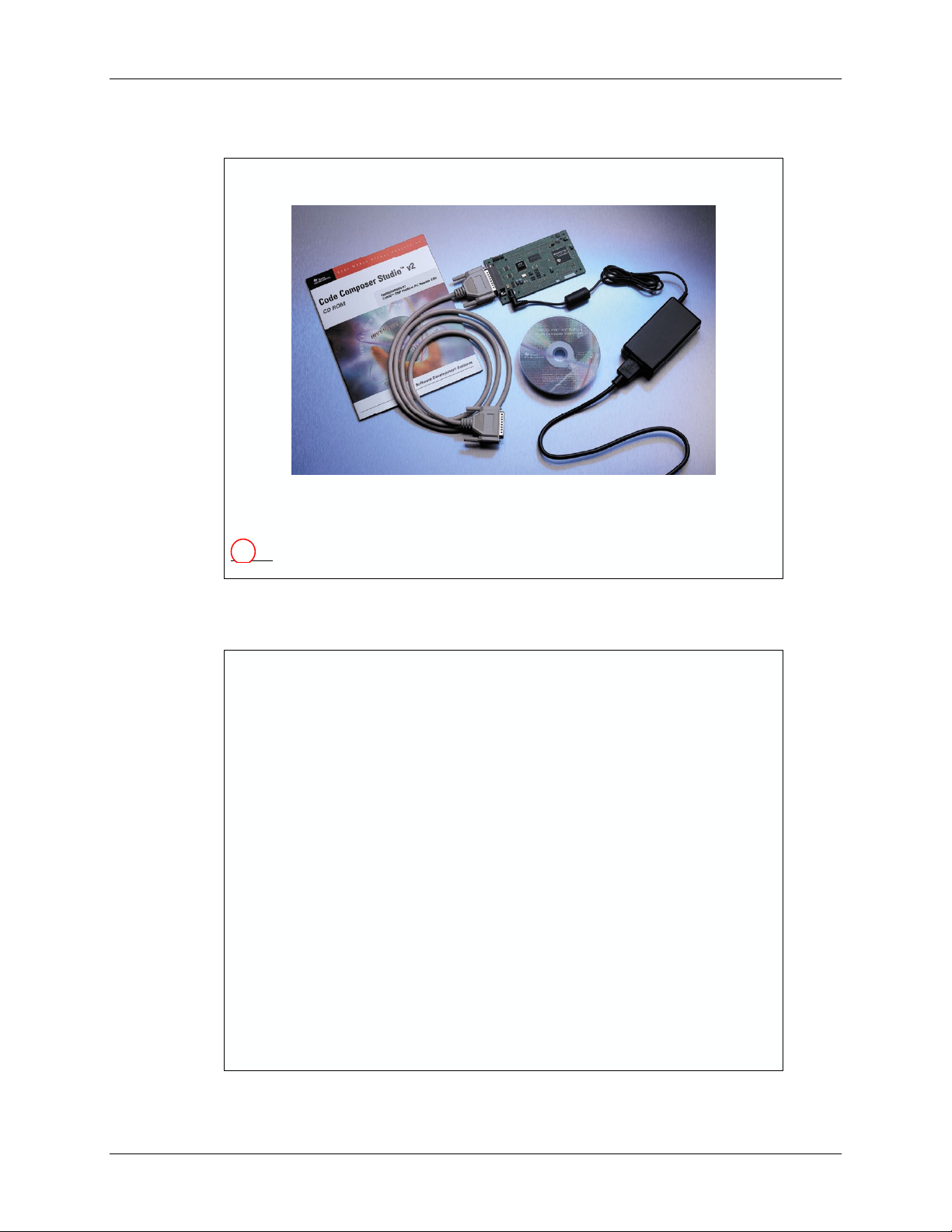
eZdsp™ F2812 Starter Kit
Texas Instruments
Texas Instruments
Technical Training
Technical Training
TO
TTTO
Technical Training
Technical Training
Organization
Organization
eZdsp
is a trademark of Spectrum Digital, Inc.
eZdsp
is a trademark of Spectrum Digital, Inc.
Introductions
Name
Name
Company
Company
Project Responsibilities
Project Responsibilities
DSP / Microcontroller Experience
DSP / Microcontroller Experience
TMS320 DSP Experience
TMS320 DSP Experience
Hardware / Software --
Hardware / Software
Interests
Interests
Copyright © 2004 Texas Instruments. All rights reserved.
Copyright © 2004 Texas Instruments. All rights reserved.
Introductions
Introductions
Assembly / C
Assembly / C
C28x - Introduction iii
Page 4
C28x Workshop
C28x Workshop Outline
C28x Workshop Outline
C28x Workshop Outline
Architecture Overview
1.1.Architecture Overview
Programming Development Environment
2.2.Programming Development Environment
Peripheral Register Header Files
3.3.Peripheral Register Header Files
Reset and Interrupts
4.4.Reset and Interrupts
System Initialization
5.5.System Initialization
Analog--toto--
6.6.Analog
Event Manager
7.7.Event Manager
Numerical Concepts and IQ Math
8.8.Numerical Concepts and IQ Math
Using DSP/BIOS
9.9.Using DSP/BIOS
10.
System Design
10.
System Design
11.
Communications
11.
Communications
12.
Support Resources
12.
Support Resources
Digital Converter
Digital Converter
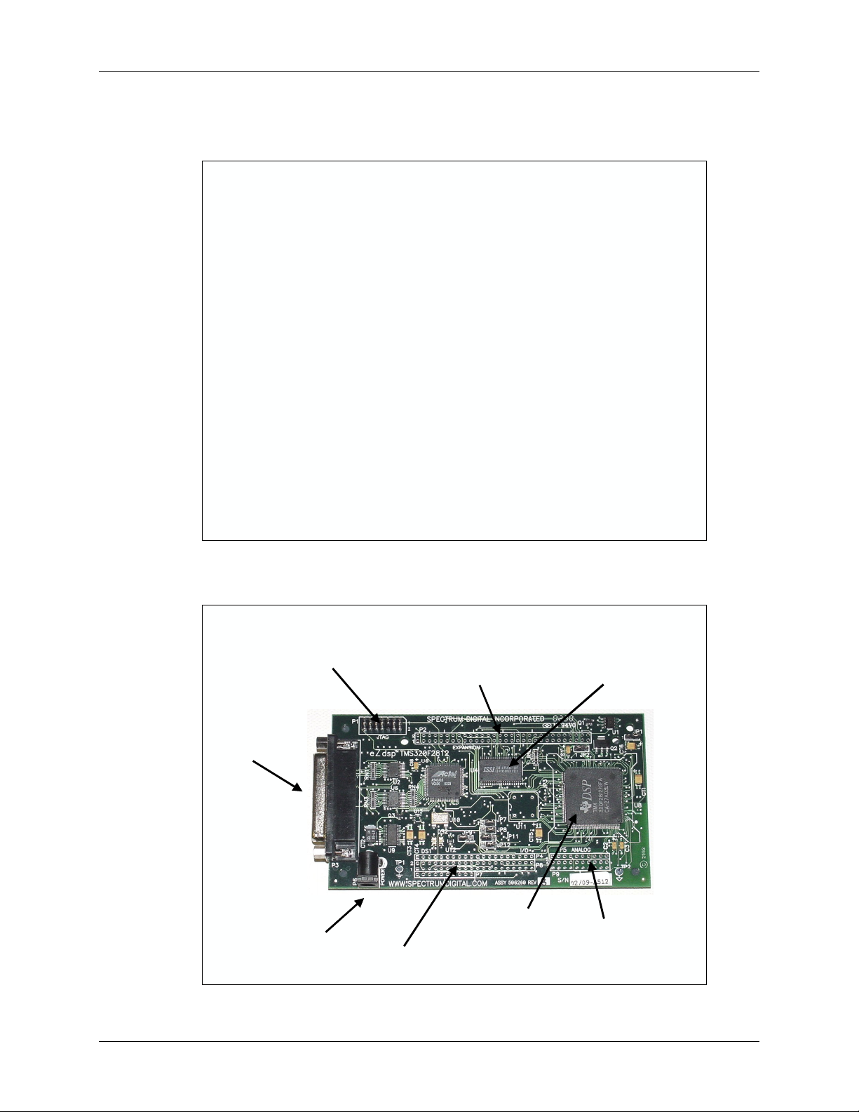
eZdsp™ F2812 Hardware
JTAG Interface (P1)
JTAG Interface (P1)
Parallel Port/
Parallel Port/
JTAG
JTAG
Controller
Controller
Interface (P3)
Interface (P3)
eZdsp
eZdsp
™ F2812 Hardware
™ F2812 Hardware
EXPANSION
EXPANSION
Data & Address (P2)
Data & Address (P2)
SRAM
SRAM
64K x 16
64K x 16
TMS320F2812 --
Power
Power
Connector (P6)
Connector (P6)
+5V
+5V
iv C28x - Introduction
I/O Interface (P4/P8/P7)
I/O Interface (P4/P8/P7)
TMS320F2812
DSP
DSP
ANALOG
ANALOG
Interface (P5/P9)
Interface (P5/P9)
Page 5

Introduction
This architecture overview introduces the basic architecture of the TMS320C28x (C28x) series of
Digital Signal Processors from Texas Instruments. The C28x series adds a new level of general
purpose processing ability unseen in any previous DSP chips. The C28x is ideal for applications
combining DSP, standard microcontroller processing, efficient C code execution, or operating
system tasks.
Learning Objectives
When this module is complete, you should have a basic understanding of the C28x architecture
and how all of its components work together to create a high-end, uniprocessor control system.
Learning Objectives
Learning Objectives
Identify the three main components
Identify the three main components
Architecture Overview
of the C28x
of the C28x
List the key features of the C28x
List the key features of the C28x
CPU
CPU
Identify the memory capabilities of
Identify the memory capabilities of
the C28x
the C28x
Identify the peripherals available on
Identify the peripherals available on
the C28x
the C28x
C28x - Architecture Overview 1 - 1
Page 6

Module Topics
Module Topics
Architecture Overview.............................................................................................................................. 1-1
Module Topics......................................................................................................................................... 1-2
What is the TMS320C28x?...................................................................................................................... 1-3
C28x CPU............................................................................................................................................... 1-4
Multiplier, ALU, and Shifters............................................................................................................. 1-5
TMS320C28x Internal Bussing .......................................................................................................... 1-6
Special Instructions............................................................................................................................. 1-7
Pipeline Advantage............................................................................................................................. 1-8
Memory ................................................................................................................................................... 1-9
Memory Map...................................................................................................................................... 1-9
Code Security Module (CSM)...........................................................................................................1-10
Peripherals .........................................................................................................................................1-10
Fast Interrupt Response.........................................................................................................................1-11
C28 Mode...............................................................................................................................................1-12
Reset.......................................................................................................................................................1-13
Summary ................................................................................................................................................1-14
1 - 2 C28x - Architecture Overview
Page 7
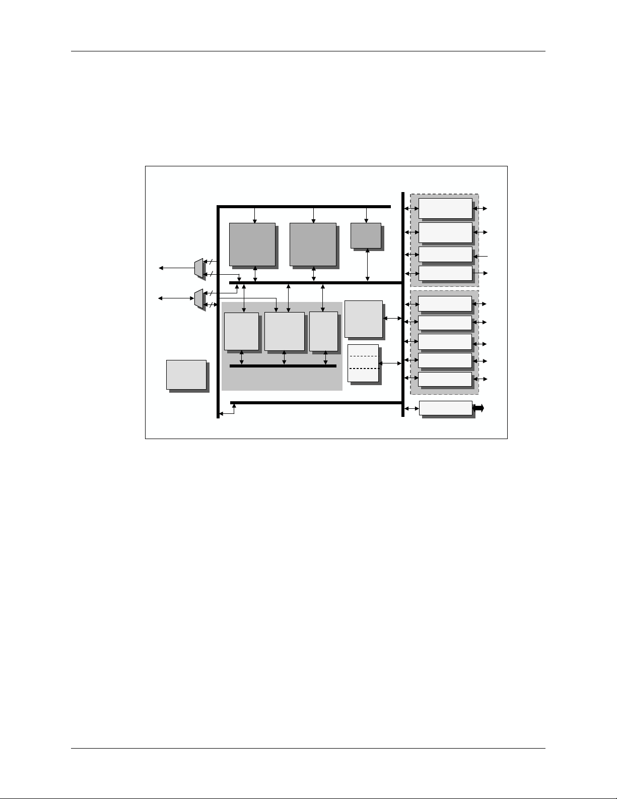
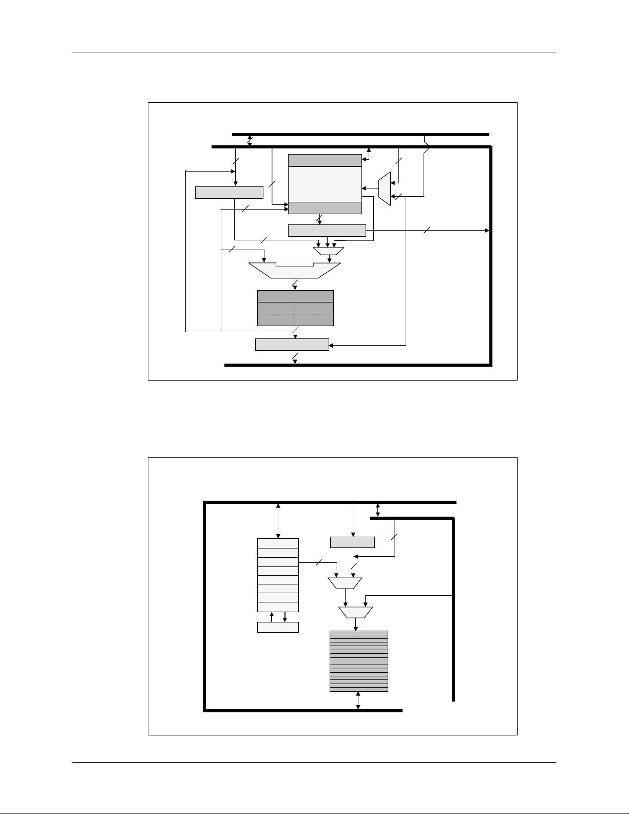
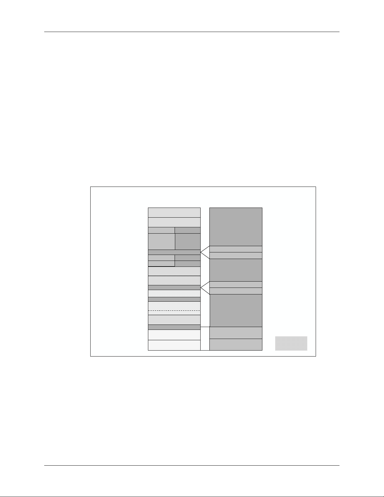
What is the TMS320C28x?
What is the TMS320C28x?
The TMS320C28x is a 32-bit fixed point DSP that specializes in high performance control
applications such as, robotics, industrial automation, mass storage devices, lighting, optical
networking, power supplies, and other control applications needing a single processor to solve a
high performance application.
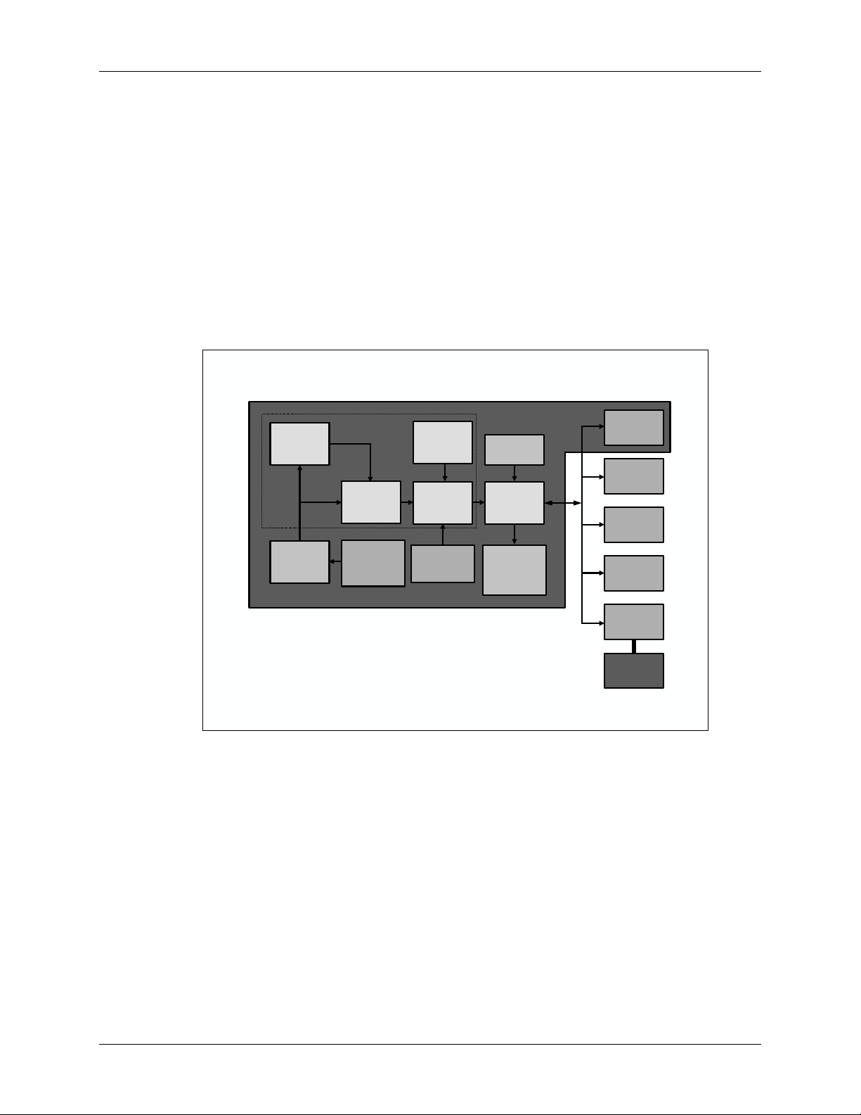
C28x Block Diagram
C28x Block Diagram
Program Bus
A(18--0)0)
A(18
D(15--0)0)
D(15
Realtime
Realtime
Realtime
JTAG
JTAG
JTAG
22
22
32
32
32
32
32
32
Sectored
Sectored
Sectored
Flash
Flash
Flash
bit
3232--bit
32-bit
Auxiliary
Auxiliary
Auxiliary
Registers
Registers
Registers
Program Bus
32x32 bit
32x32 bit
32x32 bit
Multiplier
Multiplier
Multiplier
Register Bus
Register Bus
CPU
CPU
RAM
RAM
RAM
RR--MM--W
R-M-W
Atomic
Atomic
Atomic
ALU
ALU
ALU
W
Boot
Boot
Boot
ROM
ROM
ROM
PIE
PIE
Interrupt
Interrupt
Manager
Manager
3
3
3
32 bit
32 bit
32 bit
Timers
Timers
Timers
Event
Event
Event
Manager A
Manager A
Manager A
Event
Event
Event
Manager B
Manager B
Manager B
bit ADC
1212--bit ADC
12-bit ADC
Watchdog
Watchdog
Watchdog
McBSP
McBSP
McBSP
CAN2.0B
CAN2.0B
CAN2.0B
SCI--AA
SCI
SCI-A
SCI--BB
SCI
SCI-B
SPI
SPI
SPI
Data Bus
Data Bus
The C28x architecture can be divided into 3 functional blocks:
• CPU and busing
• Memory
• Peripherals
GPIO
GPIO
GPIO
C28x - Architecture Overview 1 - 3
Page 8
C28x CPU
C28x CPU
The C28x is a highly integrated, high performance solution for demanding control applications.
The C28x is a cross between a general microcontroller and a digital signal processor, balancing
the code density of a RISC chip and the execution speed of a DSP with the architecture,
firmware, and development tools of a microcontroller.
The DSP features include a modified Harvard architecture and circular addressing. The RISC
features are single-cycle instruction execution, register-to-register operations, and modified
Harvard architecture. The microcontroller features include ease of use through an intuitive
instruction set, byte packing and unpacking, and bit manipulation.
bit
3232--bit
32-bit
Auxiliary
Auxiliary
Auxiliary
Registers
Registers
Registers
Realtime
Realtime
Realtime
JTAG
JTAG
JTAG
Program Bus
Program Bus
32x32 bit
32x32 bit
32x32 bit
Multiplier
Multiplier
Multiplier
Register Bus
Register Bus
CPU
CPU
Data Bus
Data Bus
W
RR--MM--W
R-M-W
Atomic
Atomic
Atomic
ALU
ALU
ALU
C28x CPU
C28x CPU
MCU/DSP balancing code density
MCU/DSP balancing code density
& execution time.
& execution time.
PIE
PIE
Interrupt
Interrupt
Manager
Manager
3
3
3
32 bit
32 bit
32 bit
Timers
Timers
Timers
3232--bit fixed
32 x 32 bit fixed--
32 x 32 bit fixed
Dual 16 x 16 single--
Dual 16 x 16 single
point MAC (DMAC)
point MAC (DMAC)
3232--/64
64/32 and 32/32 modulus division
64/32 and 32/32 modulus division
Fast interrupt service time
Fast interrupt service time
Single cycle read--
Single cycle read
instructions
instructions
Unique real--
Unique real
capabilities
capabilities
Upward code compatibility
Upward code compatibility
Supports 32--
Supports 32
for improved execution time;
for improved execution time;
Supports 16--
Supports 16
for improved code efficiency
for improved code efficiency
bit fixed--
/64--
bit saturation
bit saturation
bit instructions
bit instructions
bit instructions
bit instructions
point DSP
point DSP
point MAC
point MAC
cycle fixed--
cycle fixed
modify--
modify
time debugging
time debugging
write
write
The C28x design supports an efficient C engine with hardware that allows the C compiler to
generate compact code. Multiple busses and an internal register bus allow an efficient and
flexible way to operate on the data. The architecture is also supported by powerful addressing
modes, which allow the compiler as well as the assembly programmer to generate compact code
that is almost one to one corresponded to the C code.
The C28x is as efficient in DSP math tasks as it is in system control tasks that typically are
handled by microcontroller devices. This efficiency removes the need for a second processor in
many systems.
The C28x is one of several members of the fixed-point generations of digital signal processors
(DSPs) in the TMS320 family. The C28x is source-code and object-code compatible with the
C27x. In addition, the C28x is source code compatible with the 24x/240x DSP and previously
written code can be reassembled to run on a C28x device. This allows for migration of existing
code onto the C28x.
1 - 4 C28x - Architecture Overview
Page 9
C28x CPU
Multiplier, ALU, and Shifters
C28x Multiplier and ALU / Shifters
C28x Multiplier and ALU / Shifters
Program Bus
Program Bus
Data Bus
Data Bus
Shift R/L (0--
Shift R/L (0
Data Bus
Data Bus
32
32
16/32
XT (32) or T/TL
16
16
16)
16)
32
32
32
32
32
32
AH (16)
AH (16)
AH.MSB AH.LSB
AH.MSB AH.LSB
Shift R/L (0--
Shift R/L (0
XT (32) or T/TL
MULTIPLIER
MULTIPLIER
32
32
Dual 16 x 16
Dual 16 x 16
P (32) or PH/PL
P (32) or PH/PL
Shift R/L (0--
Shift R/L (0
ALU (32)
ALU (32)
32
32
ACC (32)
ACC (32)
AL (16)
AL (16)
AL.MSB AL.LSB
AL.MSB AL.LSB
32
•
32
•
32
32
32 x 32 or
32 x 32 or
32
32
16)
16)
16)
16)
16/32
8/16
8/16
•
•
32
32
The 32 x 32-bit MAC capabilities of the C28x and its 64-bit processing capabilities, enable the
C28x to efficiently handle higher numerical resolution problems that would otherwise demand a
more expensive floating-point processor solution. Along with this is the capability to perform
two 16 x 16-bit multiply accumulate instructions simultaneously or Dual MACs (DMAC).
C28x
C28x
XARn
XARn
XARn →→3232--
XARn
ARn→→1616--
ARn
XAR0
XAR0
XAR1
XAR1
XAR2
XAR2
XAR3
XAR3
XAR4
XAR4
XAR5
XAR5
XAR6
XAR6
XAR7
XAR7
ARAU
ARAU
bits
bits
bits
bits
, DP and Memory
, DP and Memory
Data Bus
Data Bus
Program Bus
Program Bus
6 LSB
6 LSB
from IR
from IR
32
32
Data Memory
Data Memory
DP (16)
DP (16)
22
22
MUX
MUX
MUX
MUX
C28x - Architecture Overview 1 - 5
Page 10
C28x CPU
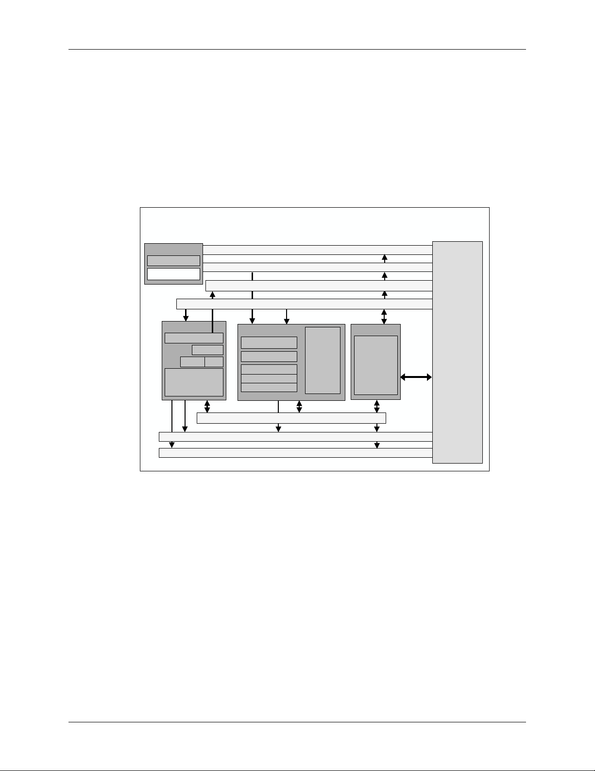
TMS320C28x Internal Bussing
As with many DSP type devices, multiple busses are used to move data between the memories
and peripherals and the CPU. The C28x memory bus architecture contains:
• A program read bus (22 bit address line and 32 bit data line)
• A data read bus (32 bit address line and 32 bit data line)
• A data write bus (32 bit address line and 32 bit data line)
C28x Internal Bus Structure
C28x Internal Bus Structure
Program
Program
PC
PC
Decoder
Decoder
Registers
Registers
ARAU
ARAU
SP
DPDP@X
XAR0
XAR0
to
to
XAR7
XAR7
SP
@X
Program Address Bus (22)
Program Address Bus (22)
Program--
Program
Data--
Data
Data--
Data
Execution
Execution
MPY32x32
MPY32x32
ALU
ALU
XT
XT
P
P
ACC
ACC
read Data Bus (32)
read Data Bus (32)
read Address Bus (32)
read Address Bus (32)
read Data Bus (32)
read Data Bus (32)
RR--MM--W
Atomic
Atomic
ALU
ALU
W
Debug
Debug
Real--
Time
Real
Time
Emulation
Emulation
&
&
Test
Test
Engine
Engine
JTAG
JTAG
Program
Program
(4M* 16)
(4M* 16)
Data
Data
(4G * 16)
(4G * 16)
Memory
Memory
Standard
Standard
Peripherals
Peripherals
External
Register Bus / Result Bus
Register Bus / Result Bus
Data/Program--
Data/Program
Data--
Data
write Data Bus (32)
write Data Bus (32)
write Address Bus (32)
write Address Bus (32)
External
Interfaces
Interfaces
The 32-bit-wide data busses enable single cycle 32-bit operations. This multiple bus architecture,
known as a Harvard Bus Architecture enables the C28x to fetch an instruction, read a data value
and write a data value in a single cycle. All peripherals and memories are attached to the memory
bus and will prioritize memory accesses.
1 - 6 C28x - Architecture Overview
Page 11
C28x CPU
Special Instructions
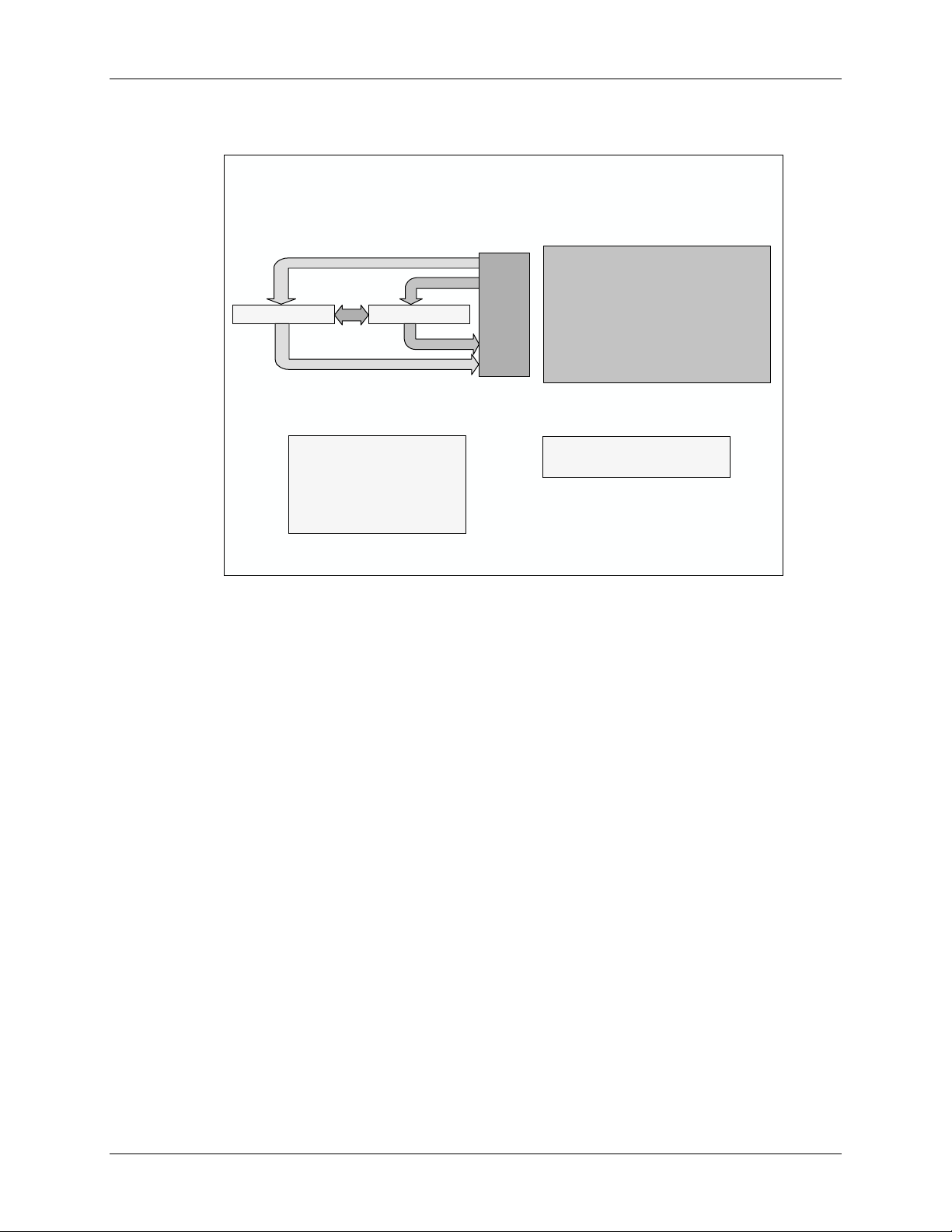
C28x Atomic Read/Modify/Write
C28x Atomic Read/Modify/Write
Atomic Instructions Benefits:
Atomic Instructions Benefits:
LOAD
Registers
Registers
CPU
CPU
LOAD
ALU / MPY
ALU / MPY
STORE
STORE
READ
READ
WRITE
WRITE
Mem
Mem
Simpler programming
¾
¾
Simpler programming
¾
Smaller, faster code
¾
Smaller, faster code
Uninterruptible (Atomic)
¾
¾
Uninterruptible (Atomic)
¾
More efficient compiler
¾
More efficient compiler
Standard Load/Store
Standard Load/Store
DINT
DINT
MOV
MOV
AND
AND
MOV
MOV
EINT
EINT
AL,*XAR2
AL,*XAR2
AL,#1234h
AL,#1234h
*XAR2,AL
*XAR2,AL
6 words / 6 cycles
6 words / 6 cycles
Atomic Read/Modify/Write
Atomic Read/Modify/Write
AND *XAR2,#1234h
AND *XAR2,#1234h
2 words / 1 cycles
2 words / 1 cycles
Atomics are small common instructions that are non-interuptable. The atomic ALU capability
supports instructions and code that manages tasks and processes. These instructions usually
execute several cycles faster than traditional coding.
C28x - Architecture Overview 1 - 7
Page 12
C28x CPU
Pipeline Advantage
C28x Pipeline
C28x Pipeline
F
F
D
D
R
F
F
D
2
1
1
D
1
1
F
D
F
D
2
2
F
F
F
F
1
1
F
F
1
2
1
A
A
F
B
B
C
C
D
D
E
E
F
F
G
G
H
H
F1: Instruction Address
F1: Instruction Address
F2: Instruction Content
F2: Instruction Content
D1: Decode Instruction
D1: Decode Instruction
D2: Resolve Operand Addr
D2: Resolve Operand Addr
R1: Operand Address
R1: Operand Address
R2: Get Operand
R2: Get Operand
X: CPU doing “real” work
X: CPU doing “real” work
W: store content to memory
W: store content to memory
F
2
2
1
1
2
2
1
1
R
R
R
1
1
D
R
D
R
2
2
D
D
D
D
1
1
F
D
F
D
2
2
F
F
F
F
1
1
F
F
X
X
W
2
2
1
2
2
1
1
2
2
1
1
W
W
1
R
R
R
R
D
D
D
D
1
F
F
2
2
F
F
1
1
W
X
X
2
2
R
X
R
X
1
2
1
2
R
R
R
R
2
1
2
1
Protected Pipeline
Protected Pipeline
2
1
2
D
R
D
R
2
1
2
1
D
D
D
D
1
2
1
2
F
D
F
D
2
1
2
1
F
F
F
F
1
2
1
2
Order of results are as written in
¾
¾
Order of results are as written in
source code
source code
¾
Programmer need not worry about
¾
Programmer need not worry about
the pipeline
the pipeline
stage pipeline
88--stage pipeline
W
W
X
X
W
W
R
X
2
2
1
1
2
2
1
1
W
X
W
R
X
2
2
1
1
1
1
2
2
2
2
W
X
W
R
X
R
R
X
W
R
XXW
R
R
R
R
2
2
2
1
2
1
R
R
W
X
X
2
2
2
2
R
R
1
1
R
R
R
R
R
D
D
D
D
R
R
R
D
D
D
D
E & G Access
E & G Access
same address
same address
W
X W
W
X W
W
The C28x uses a special 8-stage protected pipeline to maximize the throughput. This protected
pipeline prevents a write to and a read from the same location from occurring out of order.
This pipelining also enables the C28x to execute at high speeds without resorting to expensive
high-speed memories. Special branch-look-ahead hardware minimizes the latency for conditional
discontinuities. Special store conditional operations further improve performance.
1 - 8 C28x - Architecture Overview
Page 13
Memory
Memory
The memory space on the C28x is divided into program and data space. There are several
different types of memory available that can be used as both program or data space. They include
the flash memory, single access RAM (SARAM), expanded SARAM, and Boot ROM which is
factory programmed with boot software routines or standard tables used in math related
algorithms.
Memory Map
The C28x CPU contains no memory, but can access memory both on and off the chip. The C28x
uses 32-bit data addresses and 22-bit program addresses. This allows for a total address reach of
4G words (1 word = 16 bits) in data space and 4M words in program space. Memory blocks on
all C28x designs are uniformly mapped to both program and data space.
This memory map shows the different blocks of memory available to the program and data space.
TMS320F2812 Memory Map
TMS320F2812 Memory Map
Data
0x00 0000
0x00 0000
0x00 0400
0x00 0400
0x00 0800
0x00 0800
0x00 0D00
0x00 0D00
0x00 1000
0x00 1000
0x00 6000
0x00 6000
0x00 7000
0x00 7000
0x00 8000
0x00 8000
0x00 9000
0x00 9000
0x00 A000
0x00 A000
0x3D 7800
0x3D 7800
0x3D 7C00
0x3D 7C00
0x3D 8000
0x3D 8000
0x3F 8000
0x3F 8000
0x3F A000
0x3F A000
0x3F F000
0x3F F000
0x3F FFC0
0x3F FFC0
| Program
Data
| Program
MO SARAM (1K)
MO SARAM (1K)
M1 SARAM (1K)
M1 SARAM (1K)
PF 0 (2K)
PF 0 (2K)
PIE vector
PIE vector
(256)
(256)
ENPIE=1
ENPIE=1
PF 2 (4K)
PF 2 (4K)
PF 1 (4K)
PF 1 (4K)
LO SARAM (4K)
LO SARAM (4K)
L1 SARAM (4K)
L1 SARAM (4K)
FLASH (128K)
FLASH (128K)
128--
128
HO SARAM (8K)
HO SARAM (8K)
Boot ROM (4K)
Boot ROM (4K)
BROM vector (32)
BROM vector (32)
MP/MC=0 ENPIE=0
MP/MC=0 ENPIE=0
reserved
reserved
reserved
reserved
reserved
reserved
OTP (1K)
OTP (1K)
reserved
Bit Password
Bit Password
reserved
MP/MC=0
MP/MC=0
Data
| Program
Data
| Program
reserved
XINT Zone 0 (8K)
XINT Zone 1 (8K)
reserved
XINT Zone 2 (0.5M)
XINT Zone 6 (0.5M)
reserved
XINT Zone 7 (16K)
MP/MC=1
XINT Vector-RAM (32)
MP/MC=1 ENPIE=0
0x00 2000
0x00 2000
0x00 4000
0x00 4000
0x08 0000
0x08 0000
0x10 0000
0x10 0000
0x18 0000
0x18 0000
0x3F C000
0x3F C000
CSM: LO, L1
CSM: LO, L1
OTP, FLASH
OTP, FLASH
C28x - Architecture Overview 1 - 9
Page 14
Memory
Code Security Module (CSM)
Code Security Module
Code Security Module
Prevents reverse engineering and
Prevents reverse engineering and
protects valuable intellectual property
protects valuable intellectual property
0x00 8000
0x00 8000
0x00 9000
0x00 9000
0x00 A000
0x00 A000
0x3D 7800
0x3D 7800
0x3D 7C00
0x3D 7C00
0x3D 8000
0x3D 8000
128--
bit user defined password is stored in Flash
128
bit user defined password is stored in Flash
128
128--
bits = 2
128
bits = 2
To try 1 password every 2 cycles at 150 MHz, it
To try 1 password every 2 cycles at 150 MHz, it
would take at least 1.4 x 10
would take at least 1.4 x 10
possible combinations!
possible combinations!
128
LO SARAM (4K)
LO SARAM (4K)
L1 SARAM (4K)
L1 SARAM (4K)
reserved
OTP (1K)
OTP (1K)
reserved
FLASH (128K)
FLASH (128K)
128--
Bit Password
128
Bit Password
= 3.4 x 10
= 3.4 x 10
38
38
possible passwords
possible passwords
23
23
years to try all
years to try all
Peripherals
The C28x comes with many built in peripherals optimized to support control applications. These
peripherals vary depending on which C28x device you choose.
• Event Manager
• Analog-to-Digital Converter
• Watchdog Timer
• SPI
• SCI
• CAN
• McBSP
• GPIO
1 - 10 C28x - Architecture Overview
Page 15
Fast Interrupt Response
Fast Interrupt Response
The fast interrupt response, with automatic context save of critical registers, resulting in a device
that is capable of servicing many asynchronous events with minimal latency. C28x implements a
zero cycle penalty to do 14 registers context saved and restored during an interrupt. This feature
helps reduces the interrupt service routine overheads.
C28x Fast Interrupt Response Manager
C28x Fast Interrupt Response Manager
96 dedicated PIE
¾
¾
96 dedicated PIE
vectors
vectors
No software decision
¾
¾
No software decision
96
96
PIE module
PIE module
For 96
For 96
interrupts
interrupts
PIE
PIE
Register
Register
Map
Map
INT1 to
INT1 to
INT12
INT12
12 interrupts
12 interrupts
28x CPU Interrupt logic
28x CPU Interrupt logic
IFR
IER
IFR
IER
INTM
INTM
28x
28x
CPU
CPU
making required
making required
Direct access to RAM
¾
¾
Direct access to RAM
vectors
vectors
Auto flags update
¾
¾
Auto flags update
Concurrent auto
¾
¾
Concurrent auto
context save
context save
Auto Context Save
Auto Context Save
T
T
AH
AH
PH
PH
AR1 (L)
AR1 (L)
DP
DP
DBSTAT
DBSTAT
PC(msw)
PC(msw)
ST0
ST0
AL
AL
PL
PL
AR0 (L)
AR0 (L)
ST1
ST1
IER
IER
PC(lsw)
PC(lsw)
Peripheral Interrupts 12x8 = 96
Peripheral Interrupts 12x8 = 96
C28x - Architecture Overview 1 - 11
Page 16
C28 Mode
C28 Mode
The C28x is one of several members of the fixed-point generations of digital signal processors
(DSPs) in the TMS320 family. The C28x is source-code and object-code compatible with the
C27x. In addition, the C28x is source code compatable with the 24x/240x DSP and previously
written code can be reassembled to run on a C28x device. This allows for migration of existing
code onto the C28x.
C28x / C24x Modes
C28x / C24x Modes
Mode Type
Mode Type
C24x Mode
C24x Mode
C28x Mode
C28x Mode
Test Mode (default)
Test Mode (default)
Reserved
Reserved
C24x source--
¾
¾
C24x source
Allows you to run C24x source code which has been reassembled
¾
¾
Allows you to run C24x source code which has been reassembled
using the C28x code generation tools (need new vectors)
using the C28x code generation tools (need new vectors)
C28x mode:
¾
¾
C28x mode:
Can take advantage of all the C28x native features
¾
¾
Can take advantage of all the C28x native features
compatible mode:
compatible mode:
Mode Bits
Mode Bits
OBJMODE AMODE
OBJMODE AMODE
1
1
1
1
0 00
0
0 11
0
1
1
0
0
Compiler
Compiler
Option
Option
v28 --
m20
--v28
m20
v28
--v28
v27
--v27
(workshop)
(workshop)
1 - 12 C28x - Architecture Overview
Page 17
Reset
Reset
Reset ––
Reset
Reset
Reset
OBJMODE=0 AMODE=0
OBJMODE=0 AMODE=0
ENPIE=0 VMAP=1
ENPIE=0 VMAP=1
XMPNMC=0
XMPNMC=0
(microcomputer mode)
(microcomputer mode)
Reset vector fetched
Reset vector fetched
from boot ROM
from boot ROM
0x3F FFC0
0x3F FFC0
Note:
Note:
Details of the various boot options will be
Details of the various boot options will be
discussed in the Reset and Interrupts module
discussed in the Reset and Interrupts module
Bootloader
Bootloader
Bootloader
Bootloader
OBJMODE = 1
OBJMODE = 1
AMODE = 0
AMODE = 0
Boot determined by
Boot determined by
state of GPIO pins
state of GPIO pins
Execution
Execution
Entry Point
Entry Point
H0 SARAM
H0 SARAM
sets
sets
C28x - Architecture Overview 1 - 13
Page 18

Summary
Summary
Summary
Summary
High performance 32--
High performance 32
32 x 32 bit or dual 16 x 16 bit MAC
32 x 32 bit or dual 16 x 16 bit MAC
bit DSP
bit DSP
Atomic read--
Atomic read
stage fully protected pipeline
88--stage fully protected pipeline
Fast interrupt response manager
Fast interrupt response manager
128Kw on--
128Kw on
Code security module (CSM)
Code security module (CSM)
Two event managers
Two event managers
bit ADC module
1212--bit ADC module
56 shared GPIO pins
56 shared GPIO pins
Watchdog timer
Watchdog timer
Communications peripherals
Communications peripherals
modify--
modify
chip flash memory
chip flash memory
write instructions
write instructions
1 - 14 C28x - Architecture Overview
Page 19

Programming Development Environment
Introduction
This module will explain how to use Code Composer Studio (CCS) integrated development
environment (IDE) tools to develop a program. Creating projects and setting building options
will be covered. Use and the purpose of the linker command file will be described. Additionally,
the DSP/BIOS Configuration Tool will be used to handle system memory and system setup.
Learning Objectives
Learning Objectives
Learning Objectives
Use Code Composer Studio to:
Use Code Composer Studio to:
Create a
Create a
Set
Build Options
Set
Build Options
Project
Project
Create a
Create a
Describes a system’s available memory
Describes a system’s available memory
Indicates where sections will be placed
Indicates where sections will be placed
in memory
in memory
Use
Use
DSP/BIOS Configuration Tool
DSP/BIOS Configuration Tool
Handle system memory and system setup
Handle system memory and system setup
Create a .
Create a .
user
user
cdb
cdb
linker command file which:
linker command file which:
to:
to:
and .
and .
cmd
cmd
file
file
C28x - Programming Development Environment 2 - 1
Page 20

Module Topics
Module Topics
Programming Development Environment .............................................................................................. 2-1
Module Topics......................................................................................................................................... 2-2
Code Composer Studio ........................................................................................................................... 2-3
Software Development and COFF Concepts...................................................................................... 2-3
Projects ............................................................................................................................................... 2-5
Build Options...................................................................................................................................... 2-6
Creating a Linker Command File ........................................................................................................... 2-9
Sections .............................................................................................................................................. 2-9
Linker Command Files (.cmd).........................................................................................................2-12
Memory-Map Description .................................................................................................................2-12
Section Placement..............................................................................................................................2-14
Exercise 2a.............................................................................................................................................2-15
Summary: Linker Command File......................................................................................................2-16
Lab 2a: Linker Command File...............................................................................................................2-17
DSP/BIOS Configuration Tool...............................................................................................................2-21
Lab 2b: DSP/BIOS Configuration Tool .................................................................................................2-26
Solutions.................................................................................................................................................2-30
2 - 2 C28x - Programming Development Environment
Page 21
Code Composer Studio
Code Composer Studio
Software Development and COFF Concepts
In an effort to standardize the software development process, TI uses the Common Object File
Format (COFF). COFF has several features which make it a powerful software development
system. It is most useful when the development task is split between several programmers.
Each file of code, called a module, may be written independently, including the specification of
all resources necessary for the proper operation of the module. Modules can be written using
Code Composer Studio (CCS) or any text editor capable of providing a simple ASCII file output.
The expected extension of a source file is .ASM for assembly and .C for C programs.
Code Composer Studio
Code Composer Studio
Build
Compile
Compile
Build
lnk..
lnk
cmd
cmd
Probe In
Probe In
SIM
SIM
eZdsp™™
eZdsp
Asm
Asm
DSP/BIOS
Edit
Edit
Code Composer Studio includes:
Code Composer Studio includes:
DSP/BIOS
Config
Config
Tool
Tool
Integrated Edit/Debug GUI
Integrated Edit/Debug GUI
Code Generation Tools
Code Generation Tools
DSP/BIOS
DSP/BIOS
Link
Link
DSP/BIOS
DSP/BIOS
Libraries
Libraries
Debug
Debug
Probe Out
Probe Out
Graphs
Graphs
Profiling
Profiling
EVM
EVM
Third
Third
Party
Party
XDS
XDS
DSP
DSP
Board
Board
Code Composer Studio includes a built-in editor, compiler, assembler, linker, and an automatic
build process. Additionally, tools to connect file input and output, as well as built-in graph
displays for output are available. Other features can be added using the plug-ins capability
Numerous modules are joined to form a complete program by using the linker. The linker
efficiently allocates the resources available on the device to each module in the system. The
linker uses a command (.CMD) file to identify the memory resources and placement of where the
various sections within each module are to go. Outputs of the linking process includes the linked
object file (.OUT), which runs on the DSP, and can include a .MAP file which identifies where
each linked section is located.
The high level of modularity and portability resulting from this system simplifies the processes of
verification, debug and maintenance. The process of COFF development is presented in greater
detail in the following paragraphs.
C28x - Programming Development Environment 2 - 3
Page 22
Code Composer Studio
The concept of COFF tools is to allow modular development of software independent of
hardware concerns. An individual assembly language file is written to perform a single task and
may be linked with several other tasks to achieve a more complex total system.
Writing code in modular form permits code to be developed by several people working in parallel
so the development cycle is shortened. Debugging and upgrading code is faster, since
components of the system, rather than the entire system, is being operated upon. Also, new
systems may be developed more rapidly if previously developed modules can be used in them.
Code developed independently of hardware concerns increases the benefits of modularity by
allowing the programmer to focus on the code and not waste time managing memory and moving
code as other code components grow or shrink. A linker is invoked to allocate systems hardware
to the modules desired to build a system. Changes in any or all modules, when re-linked, create a
new hardware allocation, avoiding the possibility of memory resource conflicts.
Code Composer Studio: IDE
Code Composer Studio: IDE
Integrates
Integrates
and debug
and debug
Single--
Single
Powerful
Powerful
Automated tasks using
Automated tasks using
Built--
Built
Support TI or 3
Support TI or 3
: edit, code generation,
: edit, code generation,
click access
click access
graphing/profiling
graphing/profiling
in access to
in access to
using buttons
using buttons
BIOS
BIOS
rd
rd
party
party
tools
tools
GEL scripts
GEL scripts
functions
functions
plug--
ins
plug
ins
2 - 4 C28x - Programming Development Environment
Page 23
Code Composer Studio
Projects
Code Composer works with a project paradigm. Essentially, within CCS you create a project for
each executable program you wish to create. Projects store all the information required to build
the executable. For example, it lists things like: the source files, the header files, the target
system’s memory-map, and program build options.
The CCS Project
The CCS Project
Project (.
Project (.
Source files (by reference)
Source files (by reference)
Project settings:
Project settings:
pjt
) files contain:
pjt
) files contain:
Source (C, assembly)
Source (C, assembly)
Libraries
Libraries
DSP/BIOS configuration
DSP/BIOS configuration
Linker command files
Linker command files
Build Options (compiler and
Build Options (compiler and
assembler)
assembler)
Build configurations
Build configurations
DSP/BIOS
DSP/BIOS
Linker
Linker
The project information is stored in a .PJT file, which is created and maintained by CCS. To
create a new project, you need to select the
Project:New… menu item.
Along with the main Project menu, you can also manage open projects using the right-click
popup menu. Either of these menus allows you to Add Files… to a project. Of course, you can
also drag-n-drop files onto the project from Windows Explorer.
C28x - Programming Development Environment 2 - 5
Page 24
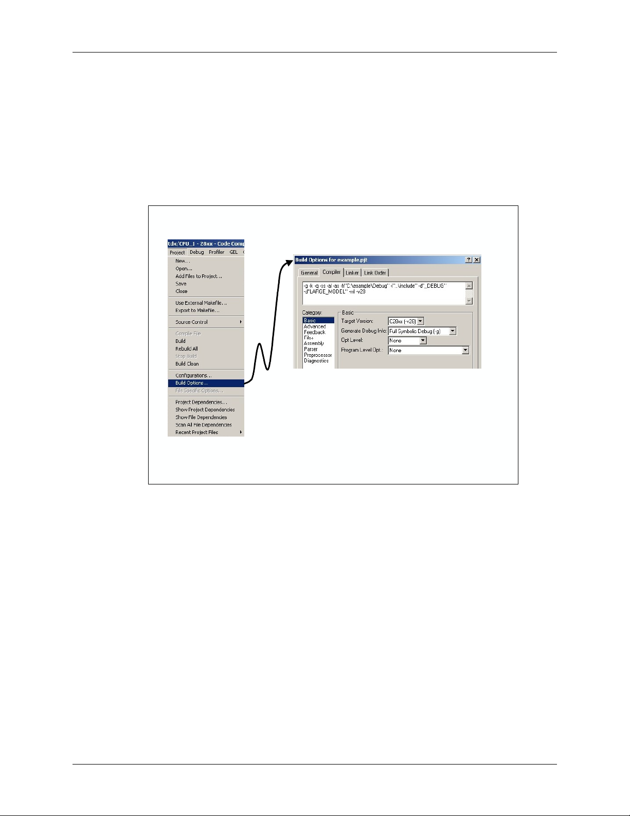
Code Composer Studio
Build Options
Project options direct the code generation tools (i.e. compiler, assembler, linker) to create code
according to your system’s needs. When you create a new project, CCS creates two sets of build
options – called Configurations: one called Debug, the other Release (you might think of as
Optimize).
To make it easier to choose build options, CCS provides a graphical user interface (GUI) for the
various compiler options. Here’s a sample of the Debug configuration options.
Build Options GUI --
Build Options GUI
GUI has 8 pages of categories for code
GUI has 8 pages of categories for code
generation tools
generation tools
Controls many aspects of the build process,
Controls many aspects of the build process,
such as:
such as:
Optimization level
Optimization level
Target device
Target device
Compiler/assembly/link options
Compiler/assembly/link options
Compiler
Compiler
There is a one-to-one relationship between the items in the text box and the GUI check and dropdown box selections. Once you have mastered the various options, you can probably find
yourself just typing in the options.
2 - 6 C28x - Programming Development Environment
Page 25
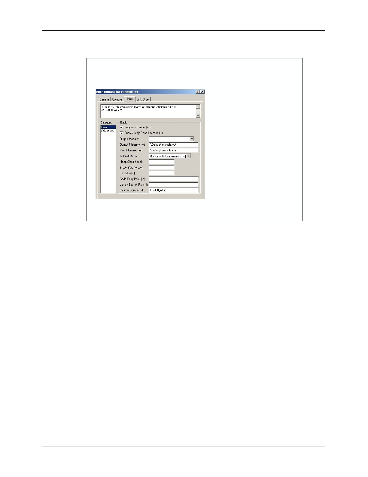
Code Composer Studio
Build Options GUI --
Build Options GUI
There are many linker options but these four handle all of the basic needs.
• -o <filename> specifies the output (executable) filename.
Linker
Linker
GUI has 2 categories
GUI has 2 categories
for linking
for linking
Specifies various link
Specifies various link
options
options
Debug\\
“.“.\\Debug
on subfolder level
on subfolder level
below project (.
below project (.
location
location
” indicates
” indicates
pjt) )
pjt
• -m <filename> creates a map file. This file reports the linker’s results.
• -c tells the compiler to autoinitialize your global and static variables.
• -x tells the compiler to exhaustively read the libraries. Without this option libraries are
searched only once, and therefore backwards references may not be resolved.
C28x - Programming Development Environment 2 - 7
Page 26
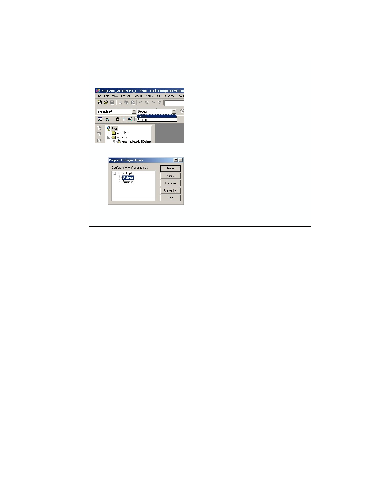
Code Composer Studio
Default Build Configurations
Default Build Configurations
For new projects, CCS automatically
For new projects, CCS automatically
creates two build configurations:
creates two build configurations:
Debug
Debug
Release
Release
Use the drop--
Use the drop
select the build configuration
select the build configuration
Add/Remove your own custom
Add/Remove your own custom
build configurations using
build configurations using
Project Configurations
Project Configurations
Edit a configuration:
Edit a configuration:
1.
Set it active
1.
Set it active
Modify build options
2.
2.
Modify build options
3.
Save project
3.
Save project
unoptimized))
((unoptimized
(optimized)
(optimized)
down menu to quickly
down menu to quickly
To help make sense of the many compiler options, TI provides two default sets of options
(configurations) in each new project you create. The Release (optimized) configuration invokes
the optimizer with –o3 and disables source-level, symbolic debugging by omitting –g (which
disables some optimizations to enable debug).
2 - 8 C28x - Programming Development Environment
Page 27
Creating a Linker Command File
Creating a Linker Command File
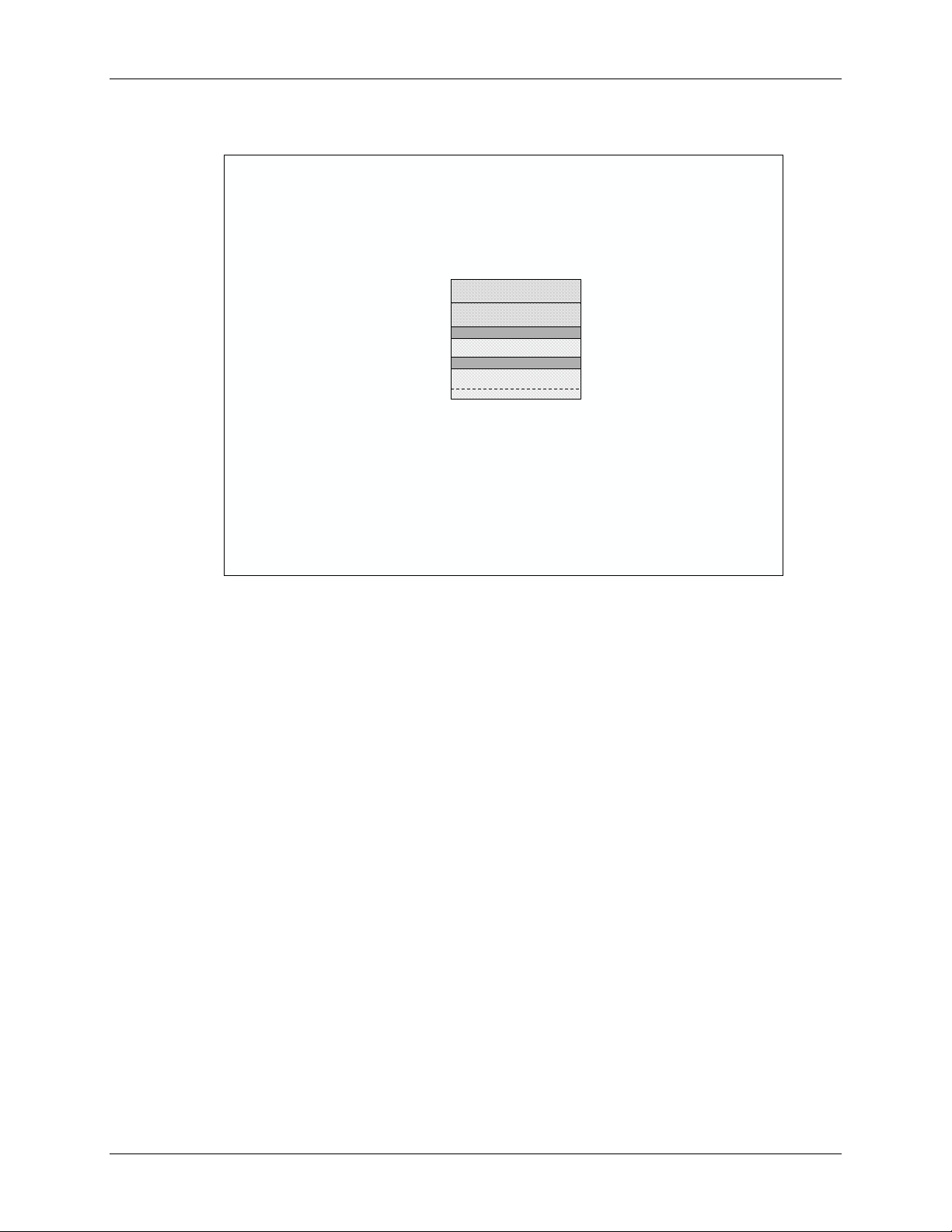
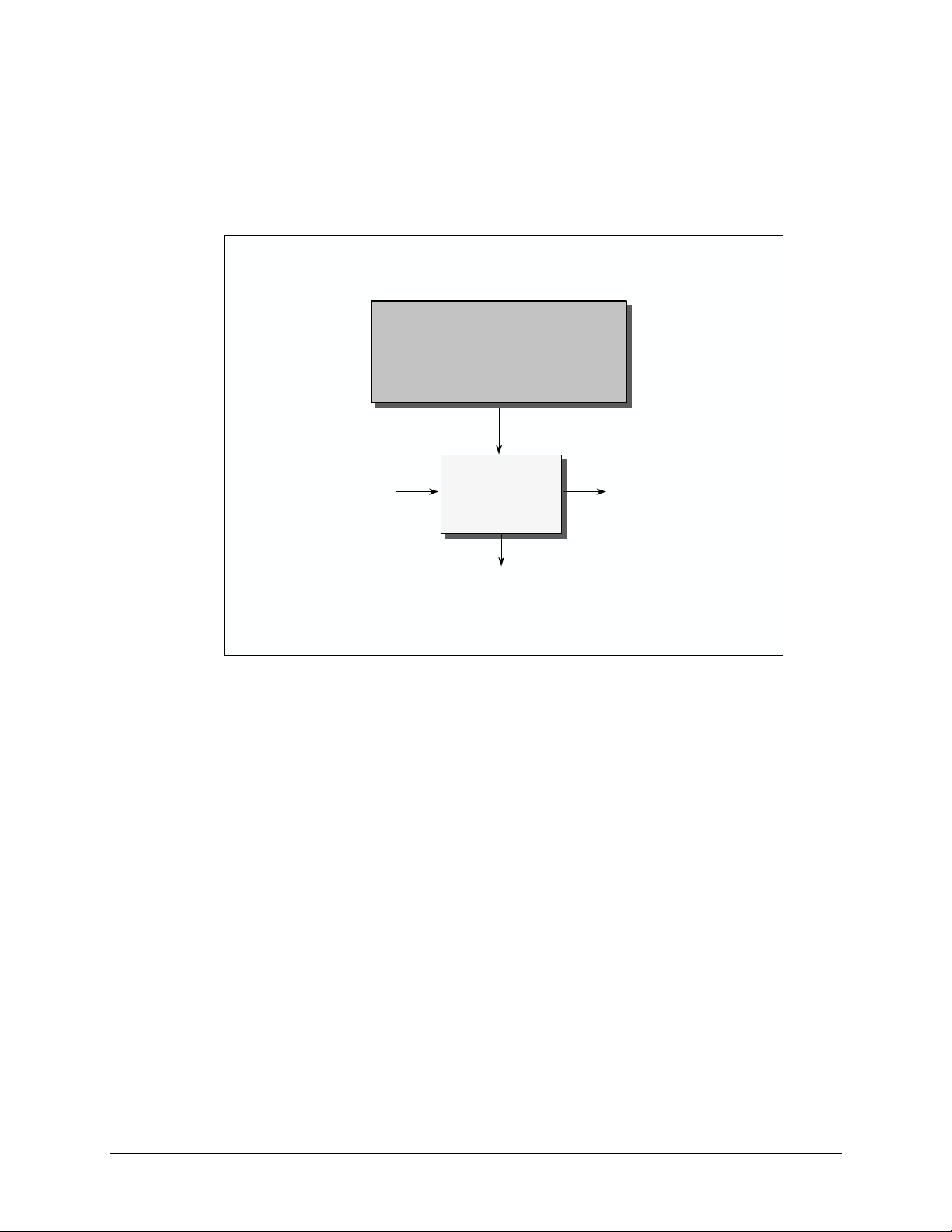
Sections
Looking at a C program, you'll notice it contains both code and different kinds of data (global,
local, etc.).
Sections
Sections
Global Vars (.
int
int
int
int
void main(void)
void main(void)
{
{
}
}
Local vars (
In the TI code-generation tools (as with any toolset based on the COFF – Common Object File
Format), these various parts of a program are called Sections. Breaking the program code and
data into various sections provides flexibility since it allows you to place code sections in ROM
and variables in RAM. The preceding diagram illustrated five sections:
• Global Variables
ebss)
ebss
x = 2;
x = 2;
y = 7;
y = 7;
long z;
long z;
z = x + y;
z = x + y;
.stack) Code (
.stack
Init vals (..
cinit)
cinit
.text)
.text
Every C program
Every C program
consists of different
consists of different
parts called
parts called
All default sections
All default sections
names begin with “.”
names begin with “.”
The compiler has
The compiler has
default sections
default sections
names for
names for
and
uninitialized
and
uninitialized
sections
sections
initialized
initialized
sections
sections
• Initial Values for global variables
• Local Variables (i.e. the stack)
• Code (the actual instructions)
C28x - Programming Development Environment 2 - 9
Page 28

Creating a Linker Command File
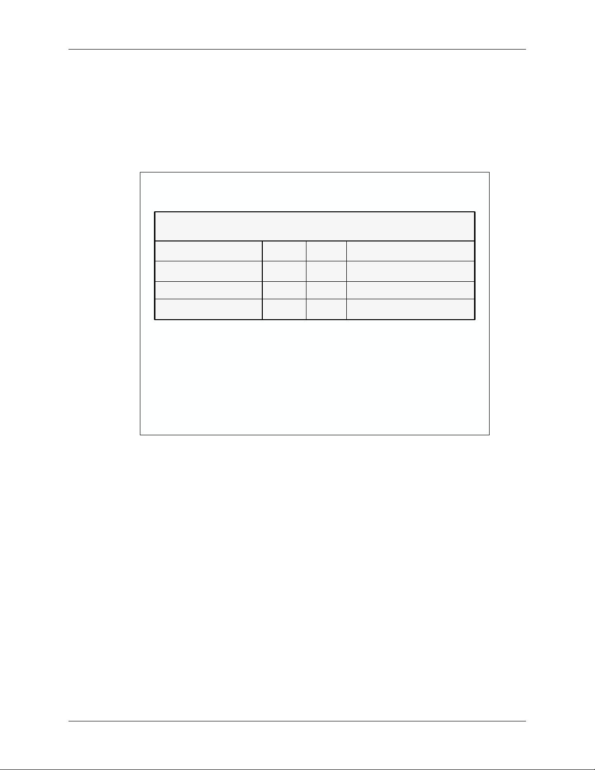
Following is a list of the sections that are created by the compiler. Along with their description,
we provide the Section Name defined by the compiler.
Initialized Sections
Initialized Sections
Name
Name
.text
.text
cinit
..cinit
econst
..econst
.switch
.switch
pinit
..pinit
Compiler Section Names
Compiler Section Names
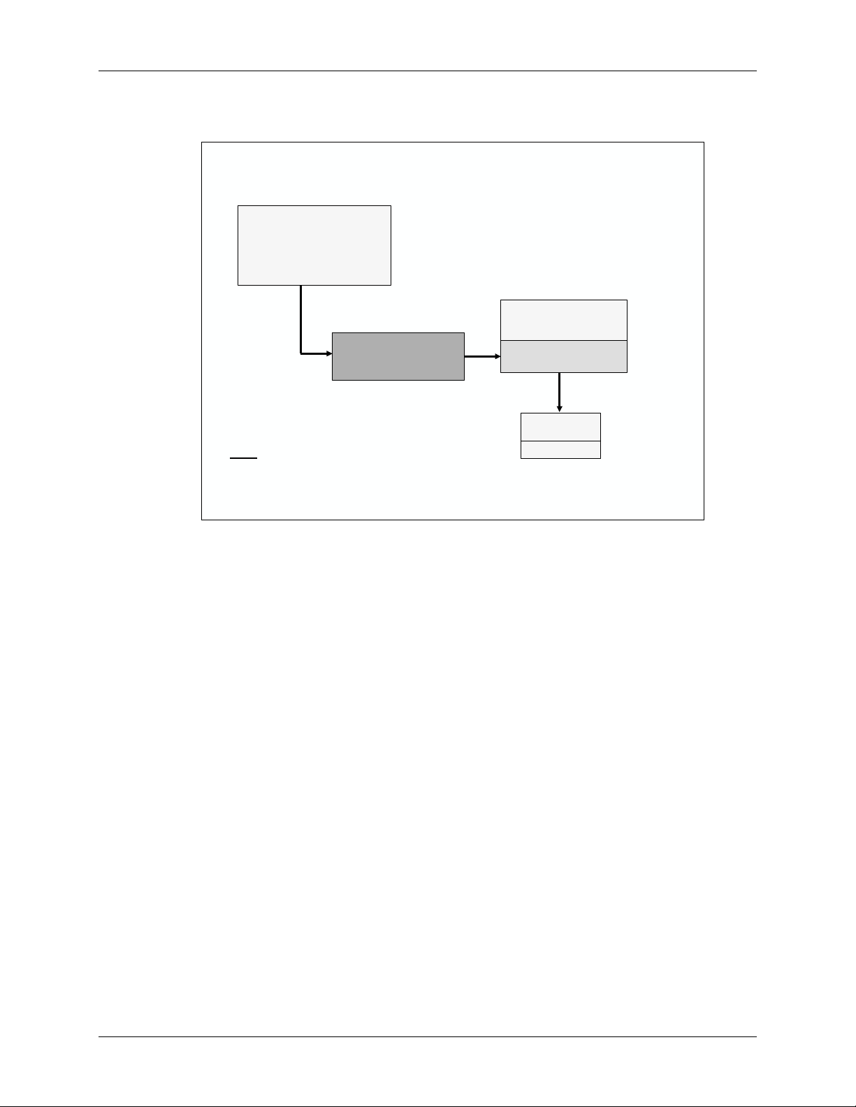
Description
Description
code
code
initialized global and static variables program
initialized global and static variables program
constant data (e.g. const
constant data (e.g. const
tables for switch statements
tables for switch statements
tables for global constructors (C++)
tables for global constructors (C++)
int
k = 3;) data
int
k = 3;) data
Link Location
Link Location
program
program
prog
/low 64K data
prog
/low 64K data
program
program
Uninitialized
Uninitialized
Name
Name
ebss
..ebss
.stack stack space
.stack stack space
esysmem
..esysmem
Sections
Sections
Description
Description
global & static variables
global & static variables
memory for far
memory for far
malloc
malloc
functions
functions
Link Location
Link Location
data
data
low 64K data
low 64K data
data
data
Sections of a C program must be located in different memories in your target system. This is the
big advantage of creating the separate sections for code, constants, and variables. In this way,
they can all be linked (located) into their proper memory locations in your target embedded
system. Generally, they’re located as follows:
Program Code (.text)
Program code consists of the sequence of instructions used to manipulate data, initialize system
settings, etc. Program code must be defined upon system reset (power turn-on). Due to this basic
system constraint it is usually necessary to place program code into non-volatile memory, such as
FLASH or EPROM.
Constants (.cinit – initialized data)
Initialized data are those data memory locations defined at reset.It contains constants or initial
values for variables. Similar to program code, constant data is expected to be valid upon reset of
the system. It is often found in FLASH or EPROM (non-volatile memory).
Variables (.ebss – uninitialized data)
Uninitialized data memory locations can be changed and manipulated by the program code during
runtime execution. Unlike program code or constants, uninitialized data or variables must reside
in volatile memory, such as RAM. These memories can be modified and updated, supporting the
way variables are used in math formulas, high-level languages, etc. Each variable must be
declared with a directive to reserve memory to contain its value. By their nature, no value is
assigned, instead they are loaded at runtime by the program
2 - 10 C28x - Programming Development Environment
Page 29
Creating a Linker Command File
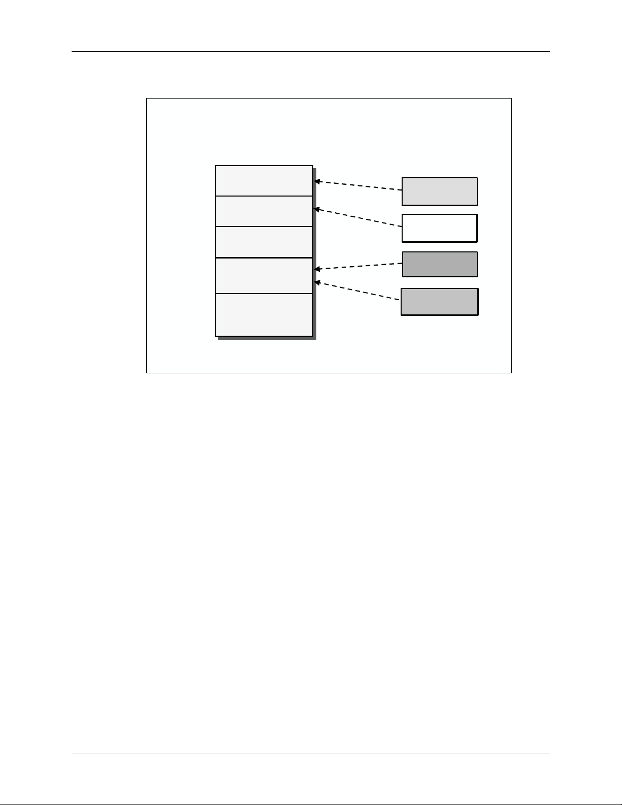
Placing Sections in Memory
Placing Sections in Memory
Memory
0x00 0000
0x00 0000
0x00 0400
0x00 0400
0x3D 8000
0x3D 8000
Memory
M0SARAM
M0SARAM
(0x400)
(0x400)
M1SARAM
M1SARAM
(0x400)
(0x400)
FLASH
FLASH
(0x20000)
(0x20000)
Sections
Sections
ebss
..ebss
.stack
.stack
cinit
..cinit
.text
.text
Linking code is a three step process:
1. Defining the various regions of memory (on-chip SARAM vs. FLASH vs. External Memory).
2. Describing what sections go into which memory regions
3. Running the linker with “build” or “rebuild”
C28x - Programming Development Environment 2 - 11
Page 30
Creating a Linker Command File
Linker Command Files (.cmd)
The linker concatenates each section from all input files, allocating memory to each section based
on its length and location as specified by the MEMORY and SECTIONS commands in the linker
command file.
Linking
Linking
Memory description
Memory description
Memory description
How to place s/w into h/w
How to place s/w into h/w
How to place s/w into h/w
obj
..obj
Link.
Link.
Linker
Linker
.map
.map
cmd
cmd
.out
.out
Memory-Map Description
Describe the memory configuration of your target system to the linker. Without this specification,
the linker might place code or data into memory that doesn’t exist.
The format is: Name: origin = 0x????, length = 0x????
For example, if you placed a 2K EPROM starting at memory location zero, it would read:
MEMORY
{
EPROM: origin = 0x0000 , length = 0x0800
}
You define each memory segment using the above format. If you added a RAM and an ABT646
transceiver, it might look like:
MEMORY
{
EPROM: origin = 0x0000 , length = 0x0800
RAM: origin = 0x1000 , length = 0x02000
ABT646: origin = 0x8000 , length = 0x00001
}
2 - 12 C28x - Programming Development Environment
Page 31

Creating a Linker Command File
Remember that the DSP has two memory maps: Program, and Data. Therefore, the MEMORY
description must describe each of these separately. The loader uses the following syntax to
delineate each of these:
Linker Page TI Definition
Page 0 Program
Page 1 Data
Linker Command File
Linker Command File
MEMORY
MEMORY
{
{
PAGE 0: /* Program Space */
PAGE 0: /* Program Space */
FLASH: org = 0x3D8000,
FLASH: org = 0x3D8000,
PAGE 1: /* Data Space */
PAGE 1: /* Data Space */
M0SARAM: org = 0x000000,
M0SARAM: org = 0x000000,
M1SARAM: org = 0x000400,
M1SARAM: org = 0x000400,
}
}
len
len
len
len
len
len
= 0x20000
= 0x20000
= 0x400
= 0x400
= 0x400
= 0x400
C28x - Programming Development Environment 2 - 13
Page 32

Creating a Linker Command File
Section Placement
You can specify how you want the sections to be distributed through memory. You would use the
following code to link the sections into the memory specified in the previous example:
SECTIONS
{
.text:> FLASH PAGE 0
.ebss:> M0SARAM PAGE 1
.cinit:> FLASH PAGE 0
.stack:> M1SARAM PAGE 1
}
The linker will gather all the code sections from all the files being linked together. Similarly, it
will combine all ‘like’ sections.
Beginning with the first section listed, the linker will place it into the specified memory segment.
Linker Command File
Linker Command File
MEMORY
MEMORY
{
{
PAGE 0:
PAGE 0:
FLASH: org = 0x3D8000,
FLASH: org = 0x3D8000,
PAGE 1:
PAGE 1:
M0SARAM: org = 0x000000,
M0SARAM: org = 0x000000,
M1SARAM: org = 0x000400,
M1SARAM: org = 0x000400,
}
}
SECTIONS
SECTIONS
{
{
.text:> FLASH PAGE 0
.text:> FLASH PAGE 0
ebss
..ebss
..cinit
.stack:>
.stack:>
}
}
:> M0SARAM PAGE 1
:> M0SARAM PAGE 1
cinit
:> FLASH PAGE 0
:> FLASH PAGE 0
/* Program Space */
/* Program Space */
len
= 0x20000
len
= 0x20000
/* Data Space */
/* Data Space */
len
= 0x400
len
= 0x400
len
= 0x400
len
= 0x400
M1SARAM
M1SARAM
PAGE 1
PAGE 1
2 - 14 C28x - Programming Development Environment
Page 33

Exercise 2a
Exercise 2a
Looking at the following block diagram, and create a linker command file.
Exercise 2a
Exercise 2a
0x00 0000
0x00 0000
0x00 8000
0x00 8000
M0SARAM
M0SARAM
(0x400)
(0x400)
L0SARAM
L0SARAM
(0x1000)
(0x1000)
0x00 0400
0x00 0400
0x00 9000
0x00 9000
M1SARAM
M1SARAM
(0x400)
(0x400)
L1SARAM
L1SARAM
(0x1000)
(0x1000)
Create the linker command file for the given memory
Create the linker command file for the given memory
map by filling in the blanks on the following slide
map by filling in the blanks on the following slide
Fill in the blanks:
0x3D 8000
0x3D 8000
F2812
F2812
Exercise 2a --
Exercise 2a
Memory
Memory
{
{
PAGE__: /* Program Space */
PAGE__: /* Program Space */
_____: org = ____
_____: org = ____
______: /* Data Space */
______: /* Data Space */
_______: org = ___
_______: org = ___
_______:
_______:
_______:
_______:
_______: org = ___
_______: org = ___
_______: org = ___
_______: org = ___
}
}
SECTIONS
SECTIONS
{
{
.text: > FLASH PAGE 0
.text: > FLASH PAGE 0
ebss
: > M1SARAM PAGE 1
..ebss
: > M1SARAM PAGE 1
cinit
..cinit
.stack: > M0SARAM PAGE 1
.stack: > M0SARAM PAGE 1
}
}
FLASH
FLASH
(0x20000)
(0x20000)
org = ____
org = ____
org = ___
org = ___
: > FLASH PAGE 0
: > FLASH PAGE 0
0x3F 8000
0x3F 8000
Command File
Command File
____,
____,
____,
____,
____,
____,
____,
____,
H0SARAM
H0SARAM
(0x2000)
(0x2000)
___,
___,
___,
___,
len
len
len
len
len
len
len
len
len
len
len
len
= ___
= ___
= _____
= _____
= _____
= _____
= __
___
= __
= _
= _
= _
= _
___
____
____
____
____
___
___
C28x - Programming Development Environment 2 - 15
Page 34

Exercise 2a
Summary: Linker Command File
The linker command file (.cmd) contains the inputs — commands — for the linker. This
information is summarized below:
Linker Command File Summary
Linker Command File Summary
Memory Map Description
Memory Map Description
Name
Name
Location
Location
Size
Size
Sections Description
Sections Description
Directs software sections into named
Directs software sections into named
memory regions
memory regions
Allows per--
Allows per
Allows separate load/run locations
Allows separate load/run locations
file discrimination
file discrimination
2 - 16 C28x - Programming Development Environment
Page 35

Lab 2a: Linker Command File
Lab 2a: Linker Command File
Objective
Create a linker command file and link the C program file (LAB2.C) into the system described
below.
Lab 2a: Linker Command File
Lab 2a: Linker Command File
Memory
Memory
chip
onon--chip
on-chip
memory
memory
memory
F2812
F2812
System Description:
System Description:
TMS320F2812
••TMS320F2812
All internal RAM blocks allocated
••All internal RAM blocks allocated
Placement of Sections:
Placement of Sections:
.text into RAM Block H0SARAM on PAGE 0 (code space)
••.text into RAM Block H0SARAM on PAGE 0 (code space)
cinit
into RAM Block H0SARAM on PAGE 0 (code space)
••..cinit
into RAM Block H0SARAM on PAGE 0 (code space)
ebss
••..ebss
••.stack into RAM Block M0SARAM on PAGE 1 (data space)
into RAM Block M1SARAM on PAGE 1 (data space)
into RAM Block M1SARAM on PAGE 1 (data space)
.stack into RAM Block M0SARAM on PAGE 1 (data space)
System Description
• TMS320F2812
• All internal RAM blocks allocated
M0SARAM
M0SARAM
M0SARAM
(0x400)
(0x400)
(0x400)
M1SARAM
M1SARAM
M1SARAM
(0x400)
(0x400)
(0x400)
H0SARAM
H0SARAM
H0SARAM
(0x2000)
(0x2000)
(0x2000)
0x00 0000
0x00 0000
0x00 0400
0x00 0400
0x3F 8000
0x3F 8000
L0SARAM
L0SARAM
L0SARAM
(0x1000)
(0x1000)
(0x1000)
L1SARAM
L1SARAM
L1SARAM
(0x1000)
(0x1000)
(0x1000)
0x00 8000
0x00 8000
0x00 9000
0x00 9000
Placement of Sections:
• .text into RAM Block H0SARAM on PAGE 0 (code space)
• .cinit into RAM Block H0SARAM on PAGE 0 (code space)
• .ebss into RAM Block M1SARAM on PAGE 1 (data space)
• .stack into RAM Block M0SARAM on PAGE 1 (data space)
Procedure
Create a New Project
1. Double click on the Code Composer Studio icon on the desktop. Maximize Code
Composer Studio to fill your screen. The menu bar (at the top) lists File ... Help. Note
the horizontal tool bar below the menu bar and the vertical tool bar on the left-hand side.
C28x - Programming Development Environment 2 - 17
Page 36

Lab 2a: Linker Command File
The window on the left is the project window and the large right hand window is your
workspace.
2. A project is all the files you will need to develop an executable output file (.out) which
can be run on the DSP hardware. Let’s create a new project for this lab. On the menu bar
click:
Project New
type Lab2 in the project name field and make sure the save in location is:
C:\C28x\LABS\LAB2. This will create a .pjt file which will invoke all the necessary
tools (compiler, assembler, linker) to build your project. It will also create a debug
folder that will hold immediate output files.
3. Add the C file to the new project. Click:
Project Add Files to Project…
and make sure you’re looking in C:\C28x\LABS\LAB2. Change the “files of type” to
view C source files (*.c) and select Lab2.c and click OPEN. This will add the file
Lab2.c to your newly created project.
4. Add Lab2a.cmd to the project using the same procedure. This file will be edited
during the lab exercise.
5. Next, add the compiler run-time support library to the project
(C:\ti\c2000\cgtools\lib\rts2800_ml.lib).
6. In the project window on the left click the plus sign (+) to the left of Project. Now,
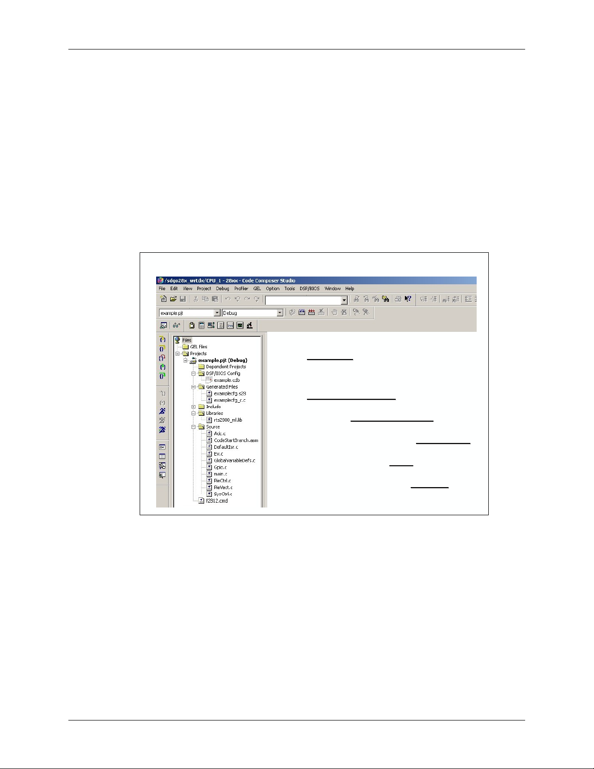
click on the plus sign next to Lab2.pjt. Notice that the Lab2a.cmd file is listed.
Click on Source to see the current source file list (i.e. Lab2.c).
Project Build Options
7. There are numerous build options in the project. The default option settings are sufficient
for getting started. We will inspect a couple of the default linker options at this time.
Click: Project Build Options…
8. Select the Linker tab. Notice that .out and .map files are being created. The .out file is
the executable code that will be loaded into the DSP. The .map file will contain a linker
report showing memory useage and section addresses in memory.
9. Set the Stack Size to 0x200. Select OK and then close the Build Options window.
Edit the Linker Command File - Lab2a.cmd
10. To open and edit Lab2a.cmd, double click on the filename in the project window.
11. Edit the Memory{} declaration by describing the system memory shown on the “Lab2a:
Linker Command File” slide.
2 - 18 C28x - Programming Development Environment
Page 37

Lab 2a: Linker Command File
12. In the Sections{} area, notice that a section called .reset has already been allocated.
The .reset section is part of the rts2800_ml.lib, and is not needed. By putting the TYPE =
DSECT modifier after its allocation, the linker will ignor this section and not allocate it.
13. Place the sections defined on the slide into the appropriate memories via the
Sections{} area. Save your work.
Build and Load the Project
14. The top four buttons on the horizontal toolbar control code generation. Hover your
mouse over each button as you read the following descriptions:
Button Name Description
1 Compile File Compile, assemble the current open file
2 Incremental Build Compile, assemble only changed files, then link
3 Rebuild All Compile, assemble all files, then link
4 Stop Build Stop code generation
15. Code Composer Studio can automatically load the output file after a successful build. On
the menu bar click: Option Customize… and select the “Program Load
Options” tab, check “Load Program After Build”, then click OK.
16. Click the “Build” button and watch the tools run in the build window. Check for
errors (we have deliberately put an error in Lab2.c). When you get an error, scroll the
build window at the bottom of the Code Composer Studio screen until you see the error
message (in red), and simply double-click the error message. The editor will
automatically open the source file containing the error, and position the mouse cursor at
the correct code line.
17. Fix the error by adding a semicolon at the end of the "z = x + y" statement. For
future knowlege, realize that a single code error can sometimes generate multiple error
messages at build time. This was not the case here.
18. Rebuild the project (there should be no errors this time). The output file should
automatically load. The Program Counter should be pointing to _c_int00 in the
Disassembly Window.
19. Under Debug on the menu bar click “Go Main”. This will run through the C-
environment initialization routine in the rts2800_ml.lib and stop at main() in
Lab2.c.
Debug Enviroment Windows
It is standard debug practice to watch local and global variables while debugging code. There
are various methods for doing this in Code Composer Studio. We will examine two of them
here: memory windows, and watch windows.
20. Open a memory window to view the global variable “z”.
Click: View Memory on the menu bar.
C28x - Programming Development Environment 2 - 19
Page 38

Lab 2a: Linker Command File
Type “&z” into the address field. Note that you must use the ampersand (meaning
"address of") when using a symbol in a memory window address box. Also note that
Code Composer Studio is case sensitive.
Set the properties format to “Hex – TI style.” This will give you more viewable data in
the window.
Click OK to close the window property selection screen. The memory window will now
open. You can change the contents of any address in the memory window by doubleclicking on its value. This is useful during debug.
21. Open the watch window to view the local variables x and y.
Click: View Watch Window on the menu bar.
Click the “Watch Locals” tab and notice that the local variables x and y are already
present. The watch window will always contain the local variables for the code function
currently being executed.
(Note that local variables actually live on the stack. You can also view local variables in
a memory window by setting the address to “SP” after the code function has been
entered).
22. We can also add global variables to the watch window if desired. Let's add the global
variable “z”.
Click the “Watch 1" tab at the bottom of the watch window. In the empty box in the
"Name" column, type “z”. Note that you do not use an ampersand here. The watch
window knows you are specifying a symbol.
Check that the watch window and memory window both report the same value for “z”.
Trying changing the value in one window, and notice that the value also changes in the
other window.
Single-stepping the Code
23. Single-step through main() by using the <F8> key (or you can use the Single
Step button on the vertical toolbar). Check to see if the program is working as
expected. What is the value for “z” when you get to the end of the program?
End of Exercise
2 - 20 C28x - Programming Development Environment
Page 39

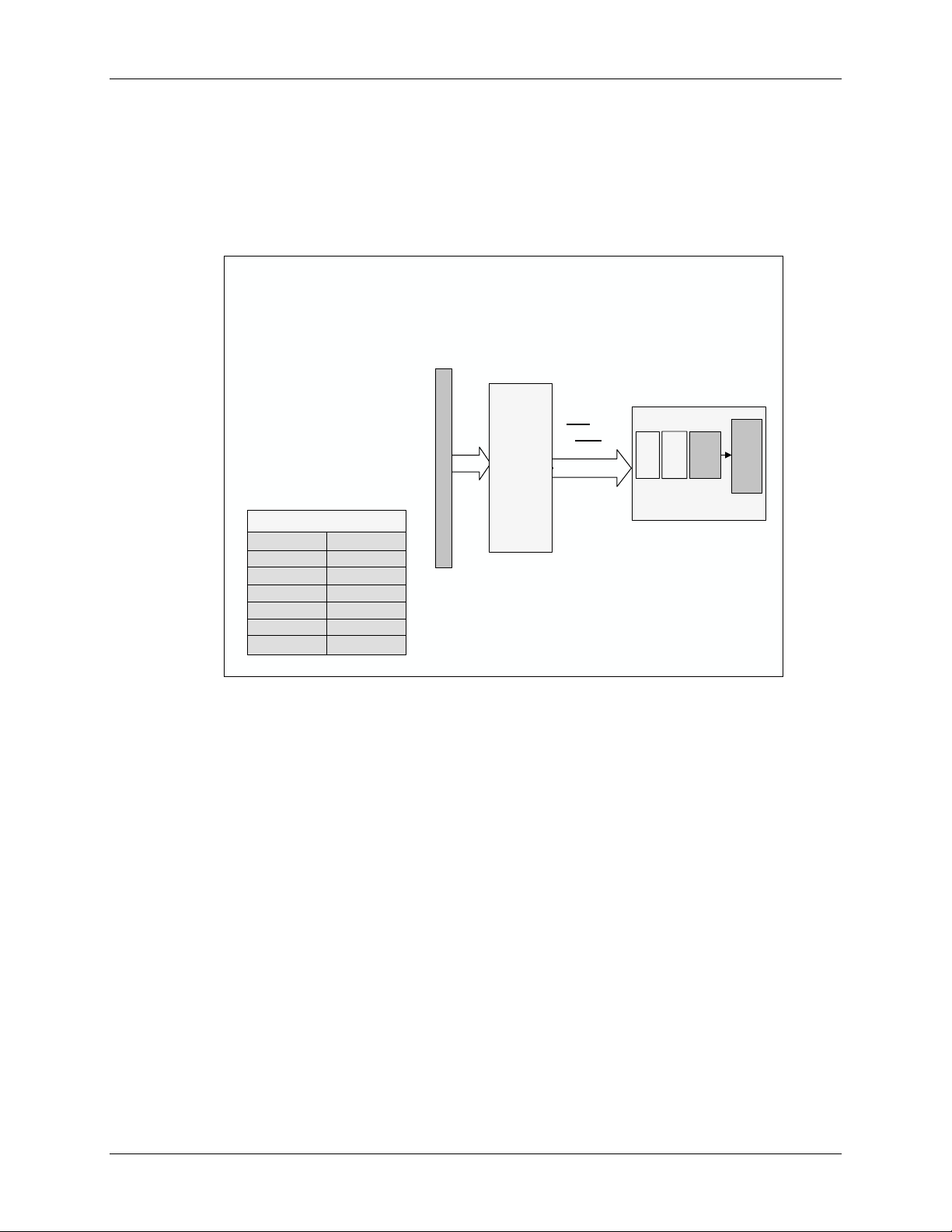
DSP/BIOS Configuration Tool
DSP/BIOS Configuration Tool
The DSP/BIOS Configuration Tool (often called Config Tool or GUI Tool or GUI) creates and
modifies a system file called the Configuration DataBase (.CDB). If we talk about using CDB
files, we’re also talking about using the Config Tool.
(file .
DSP/BIOS Configuration Tool
DSP/BIOS Configuration Tool
MEM handles system
MEM handles system
memory configuration
memory configuration
(builds .
(builds .
Configures BIOS
Configures BIOS
scheduling, RTA and
scheduling, RTA and
other BIOS functions
other BIOS functions
Automatically
Automatically
handles: run--
handles: run
support libraries,
support libraries,
interrupt vectors,
interrupt vectors,
system reset, etc.
system reset, etc.
cmd
cmd
(file .
file)
file)
time
time
cdb))
cdb
The GUI (graphical user interface) simplifies system design by:
• Automatically including the appropriate runtime support libraries
• Automatically handles interrupt vectors and system reset
• Handles system memory configuration (builds CMD file)
• When a CDB file is saved, the Config Tool generates 5 additional files:
Filename.cdb
Filenamecfg_c.c
Filenamecfg.s28
Filenamecfg.cmd
Filenamecfg.h
Filenamecfg.h28
When you add a CDB file to your project, CCS automatically adds the C and assembly
(.S28) files to the project under the Generated Files folder. (You must manually add the
CMD file, yourself.)
Configuration Database
C code created by Config Tool
ASM code created by Config Tool
Linker commands
header file for *cfg_c.c
header file for *cfg.s28
C28x - Programming Development Environment 2 - 21
Page 40

DSP/BIOS Configuration Tool
1. Creating a New Memory Region (Using MEM)
First, to create a specific memory area, open up the .CDB file, right-click on the Memory Section
Manager and select “Insert MEM”. Give this area a unique name and then specify its base and
length. Once created, you can place sections into it (shown in the next step).
Memory Section Manager
Memory Section Manager
Mem
manager allows
Mem
you to create
you to create
memory area and
memory area and
place sections
place sections
To create a new
To create a new
memory area:
memory area:
manager allows
Right--
click on MEM
Right
click on MEM
and select Insert
and select Insert
memory
memory
Fill in base, length,
Fill in base, length,
space
space
2 - 22 C28x - Programming Development Environment
Page 41

DSP/BIOS Configuration Tool
2. Placing Sections – MEM Manager Properties
The configuration tool makes it easy to place sections. The predefined compiler sections that
were described earlier each have their own drop-down menu to select one of the memory regions
you defined (in step 1).
Memory Section Manager Properties
Memory Section Manager Properties
To place a section
To place a section
into a memory area:
into a memory area:
Right--
click on MEM
Right
click on MEM
and select
and select
Properties
Properties
Select the
Select the
appropriate tab (e.g.
appropriate tab (e.g.
Compiler)
Compiler)
Select the memory
Select the memory
for each section
for each section
C28x - Programming Development Environment 2 - 23
Page 42

DSP/BIOS Configuration Tool
3. Running the Linker
Creating the Linker Command File (via .CDB)
When you have finished creating memory regions and allocating sections into these memory
areas (i.e. when you save the .CDB file), the CCS configuration tool creates five files. One of the
files is BIOS’s cfg.cmd file — a linker command file.
Files Created by
Files Created by
MEMORY{
MEMORY{
FLASH: org = 0x3D8000, len = 0x20000
FLASH: org = 0x3D8000, len = 0x20000
H0SARAM: org = 0x3F8000, len = 0x2000
H0SARAM: org = 0x3F8000, len = 0x2000
… }
… }
SECTIONS{
SECTIONS{
.text: > FLASH
.text: > FLASH
.bss: > M0SARAM
.bss: > M0SARAM
… }
… }
Config
Config
Config
Config
different files
different files
Notice, one of them is the
Notice, one of them is the
linker command file
linker command file
CMD file is generated from
CMD file is generated from
your MEM settings
your MEM settings
Tool
Tool
tool generates five
tool generates five
cfg_c.c
**cfg_c.c
cfg.s28
**cfg.s28
cfg.cmd
**cfg.cmd
cfg.h
**cfg.h
cfg.h28
**cfg.h28
This file contains two main parts, MEMORY and SECTIONS. (Though, if you open and
examine it, it’s not quite as nicely laid out as shown above.)
2 - 24 C28x - Programming Development Environment
Page 43

DSP/BIOS Configuration Tool
Running the Linker
The linker’s main purpose is to link together various object files. It combines like-named input
sections from the various object files and places each new output section at specific locations in
memory. In the process, it resolves (provides actual addresses for) all of the symbols described in
your code.
Config
Config
Tool Linker Command File
Tool Linker Command File
“Build”
app.cdb
Linker
appcfg.cmd
Linker
.obj files
libraries
(.lib)
Do not modify
Do not modify
be overwritten during “Build” (or “Rebuild”)
be overwritten during “Build” (or “Rebuild”)
The linker can create two outputs, the executable (.out) file and a report which describes the
results of linking (.map).
appcfg..
appcfg
cmd ––
cmd
your changes will
your changes will
myApp.out
.map
Note: If the graphic above wasn’t clear enough, the linker gets run automatically when you
BUILD or REBUILD your project.
C28x - Programming Development Environment 2 - 25
Page 44

Lab 2b: DSP/BIOS Configuration Tool
Lab 2b: DSP/BIOS Configuration Tool
Objective
Use Code Composer Studio and DSP/BIOS configuration tool to create a configuration database
files (*.CDB). The generated linker command file Labcfg.cmd will be then be used with Lab2.c
to verify its operation. The memory and sections of a “user” linker command file will be deleted,
however, the “user” linker command file will be needed and modified in future labs.
Lab 2b: Configuration Tool
Lab 2b: Configuration Tool
Memory
Memory
chip
onon--chip
on-chip
memory
memory
memory
F2812
F2812
System Description:
System Description:
TMS320F2812
••TMS320F2812
All internal RAM blocks allocated
••All internal RAM blocks allocated
Placement of Sections:
Placement of Sections:
.text into RAM Block H0SARAM in code space (PAGE 0)
••.text into RAM Block H0SARAM in code space (PAGE 0)
cinit
into RAM Block H0SARAM in code space (PAGE 0)
••..cinit
into RAM Block H0SARAM in code space (PAGE 0)
ebss
••..ebss
••.stack into RAM Block M0SARAM in data space (PAGE 1)
into RAM Block M1SARAM in data space (PAGE 1)
into RAM Block M1SARAM in data space (PAGE 1)
.stack into RAM Block M0SARAM in data space (PAGE 1)
System Description
• TMS320F2812
• All internal RAM blocks allocated
M0SARAM
M0SARAM
M0SARAM
(0x400)
(0x400)
(0x400)
M1SARAM
M1SARAM
M1SARAM
(0x400)
(0x400)
(0x400)
H0SARAM
H0SARAM
H0SARAM
(0x2000)
(0x2000)
(0x2000)
0x00 0000
0x00 0000
0x00 0400
0x00 0400
0x3F 8000
0x3F 8000
L0SARAM
L0SARAM
L0SARAM
(0x1000)
(0x1000)
(0x1000)
L1SARAM
L1SARAM
L1SARAM
(0x1000)
(0x1000)
(0x1000)
0x00 8000
0x00 8000
0x00 9000
0x00 9000
Placement of Sections:
• .text into RAM Block H0SARAM in code space (PAGE 0)
• .cinit into RAM Block H0SARAM in code space (PAGE 0)
• .ebss into RAM Block M1SARAM in data space (PAGE 1)
• .stack into RAM Block M0SARAM in data space (PAGE 1)
Procedure
Project Lab2.pjt
1. If Code Composer Studio is not running from the previous lab exercise, double click on
the CCS 2 (‘C2000) icon on the desktop. Maximize CCS to fill your screen. Then select
2 - 26 C28x - Programming Development Environment
Page 45

Lab 2b: DSP/BIOS Configuration Tool
Lab2.pjt from the Project Recent Project Files list. This will put you
at the proper starting point for this lab exercise.
2. If needed, verify that the project is open in CCS by left clicking the plus sign (+) to the
left of Project. Then, click on the plus sign next to Lab2.pjt ,as well as the other
plus signs to verify all the previous files have been included.
Remove “rts2800_ml.lib” and “Lab2a.cmd” from the Project
3. Highlight the rts2800_ml.lib in the project window and right click, then select
“Remove from Project”. The DSP/BIOS Config Tool supplies its own rts library.
4. Remove Lab2a.cmd using the same procedure. We will be using the DSP/BIOS
configuration tool to create a linker command file.
Using the DSP/BIOS Configuration Tool
5. The configuration database files (*.cdb), created by the Config Tool, controls a wide
range of CCS capabilities. In this lab exercise, the CDB file will be used to automatically
create and perform memory management. Create a new CDB file for this lab. On the
menu bar click:
File New DSP/BIOS Configuration…
A dialog box appears. The CDB files shown in the aforementioned dialog box are called
“seed” CDB files. CDB files are used to configure many objects specific to the
processor. Select the c28xx.cdb template and click OK.
6. Save the configuration file by selecting:
File Save As…
and name it Lab.cdb in C:\C28x\LABS\LAB2. Close the configuration window.
7. Add the configuration file to the project. Click:
Project Add Files to Project…
Make sure you’re looking in C:\C28x\LABS\LAB2. Change the “files of type” to
view All Files (*.*) and select Lab.cdb. Click OPEN to add the file to the project.
8. Add the generated linker command file, Labcfg.cmd, to the project using the same
procedure.
Create New Memory Sections Using the CDB File
9. Open the Lab.cdb file by left clicking on the plus sign (+) to the left of DSP/BIOS
Config and double clicking on the Lab.cdb file. In the configuration window, left
click the plus sign next to System and the plus sign next to MEM.
10. By default, the Memory Section Manager has combined the memory space for
L0SARAM and L1SARAM into a single memory block called L0SARAM. It has also
C28x - Programming Development Environment 2 - 27
Page 46

Lab 2b: DSP/BIOS Configuration Tool
combined M0SARAM and M1SARAM into a single memory block called M0SARAM.
We want to split these memory sections as shown in the slide for this lab exercise.
Right click on MEM – Memory Section Manager and select Insert MEM.
Rename the newly added memory section to L1SARAM. Create a second new memory
section, and rename it to M1SARAM.
11. Modify the length and base addresses of each of the memory sections L0SARAM,
L1SARAM, M0SARAM, and M1SARAM to correspond to the memory mapping shown
in the figure at the beginning of this lab. To modify the length and base address of a
memory section, right click on the memory in configuration tool, and select “Properties.”
While modifying the length and base address of each section, make sure the
“create a heap in memory” box is checked ONLY for L0SARAM. Uncheck
this box in the other three memory sections.
12. Right click on MEM – Memory Section Manager and select Properties.
Select the Compiler Sections tab and place the sections defined on the slide into
the appropriate memories via the pull-down boxes. Click OK to save your work.
Set the Stack Size in the CDB File
13. Recall in the previous lab exercise that the stack size was set using the CCS project Build
Options. When using the DSP/BIOS configuration tool, the stack size is instead specified
in the CDB file. First we need to remove the stack size setting from the project Build
Options.
14. Click: Project Build Options… and select the Linker tab. Delete the entry
for setting the Stack Size to 0x200. Select OK to close the Build Options window.
15. Right click on MEM – Memory Section Manager and select Properties.
Select the General tab. Notice that the Stack Size has been set to 0x200 by default, so
there is no need to modify this. Click OK to close the window.
Build and Load the Project
16. Click the “Build” button and watch the tools run in the build window. The output file
should automatically load. The Program Counter should be pointing to _c_int00 in
the Disassembly Window.
17. Under Debug on the menu bar click “Go Main”. This will run through the DSP/BIOS
C-environment initialization routine and stop at main() in Lab2.c.
Run the Code
18. We will verify the operation of the code using the same procedure used in Lab2a. Open
the watch window and add the global variable z.
2 - 28 C28x - Programming Development Environment
Page 47

Lab 2b: DSP/BIOS Configuration Tool
19. Next, single-step the routine through to the end. Check to see if the program is working
as expected. You should get the same value for “z” as in Lab2a.
End of Exercise
C28x - Programming Development Environment 2 - 29
Page 48

Solutions
Solutions
Exercise 2a --
Exercise 2a
Memory
Memory
{
{
PAGE00
PAGE
PAGE 1
PAGE 1
}
}
SECTIONS
SECTIONS
{
{
}
}
: /* Program Space */
: /* Program Space */
FLASH
: org =
FLASH
: org =
: /* Data Space */
: /* Data Space */
M0SARAM
M0SARAM
M1SARAM
M1SARAM
L0SARAM
L0SARAM
L1SARAM
L1SARAM
H0SARAM
H0SARAM
.text: > FLASH
.text: > FLASH
ebss
..ebss
cinit
..cinit
.stack: > M0SARAM PAGE 1
.stack: > M0SARAM PAGE 1
: org =
: org =
: org =
: org =
: org =
: org =
: org =
: org =
: org =
: org =
: > M1SARAM PAGE 1
: > M1SARAM PAGE 1
: > FLASH PAGE 0
: > FLASH PAGE 0
0x3D8000
0x3D8000
0x000000
0x000000
0x000400
0x000400
0x008000
0x008000
0x009000
0x009000
0x3F8000
0x3F8000
Solution
Solution
,
len= =
,
len
,
len= =
,
len
,
len= =
,
len
,
len= =
,
len
,
len= =
,
len
,
len= =
,
len
PAGE 0
PAGE 0
0x20000
0x20000
0x400
0x400
0x400
0x400
0x1000
0x1000
0x1000
0x1000
0x2000
0x2000
Lab 2a: Solution --
Lab 2a: Solution
MEMORY
MEMORY
{
{
PAGE 0:
PAGE 0:
H0SARAM: org = 0x3F8000,
H0SARAM: org = 0x3F8000,
PAGE 1:
PAGE 1:
M0SARAM: org = 0x000000,
M0SARAM: org = 0x000000,
M1SARAM: org = 0x000400,
M1SARAM: org = 0x000400,
L0SARAM: org = 0x008000,
L0SARAM: org = 0x008000,
L1SARAM: org = 0x009000,
L1SARAM: org = 0x009000,
}
}
SECTIONS
SECTIONS
{
{
.text: > H0SARAM PAGE 0
.text: > H0SARAM PAGE 0
ebss
: > M1SARAM PAGE 1
..ebss
..cinit
.stack: > M0SARAM PAGE 1
.stack: > M0SARAM PAGE 1
.reset: > H0SARAM PAGE 0, TYPE = DSECT
.reset: > H0SARAM PAGE 0, TYPE = DSECT
}
}
: > M1SARAM PAGE 1
cinit
: > H0SARAM PAGE 0
: > H0SARAM PAGE 0
/* Program Space */
/* Program Space */
/* Data Space */
/* Data Space */
lab2.cmd
lab2.cmd
len
= 0x2000
len
= 0x2000
len
= 0x400
len
= 0x400
len
= 0x400
len
= 0x400
len
= 0x1000
len
= 0x1000
len
= 0x1000
len
= 0x1000
2 - 30 C28x - Programming Development Environment
Page 49

Introduction
The purpose of the F281x C-code header files is to simplify the programming of the many
peripherals on the C28x device. Typically, to program a peripheral the programmer needs to
write the appropriate values to the different fields within a control register. In it’s simplest form,
the process consists of writing a hex value (or masking a bit field) to the correct address in
memory. But, since this can be a burdensome and repetitive task, the C-code header files were
created to make this a less complicated task.
The F281x C-code header files are part of a library consisting of C functions, macros, peripheral
structures, and variable definitions. Together, this set of files is known as the ‘header files.’
Eventually, the entire collection will be replaced with a CCS add-in called the Chip Support
Library (CSL). At that time, there will be a GUI interface used via CCS’s config tool.
Registers and the bit-fields are represented by structures. C functions and macros are used to
initialize or modify the structures (registers).
In this module, you will learn how to use the header files and C programs to facilitate
programming the peripherals.
Peripherial Registers Header Files
Learning Objectives
Learning Objectives
Learning Objectives
Understand the usage of the F281x
Understand the usage of the F281x
Code Header Files
CC--Code Header Files
Be able to program peripheral
Be able to program peripheral
registers
registers
Understand how peripherals are
Understand how peripherals are
mapped with linker command file
mapped with linker command file
C28x - Peripheral Registers Header Files 3 - 1
Page 50

Module Topics
Module Topics
Peripherial Registers Header Files .......................................................................................................... 3-1
Module Topics......................................................................................................................................... 3-2
Traditional and Structure Approach to C Coding ..................................................................................3-3
Naming Conventions............................................................................................................................... 3-6
Example of Peripheral Structure .h file .................................................................................................. 3-7
Mapping Structures to Memory .............................................................................................................. 3-8
Linker Command File......................................................................................................................... 3-8
F281x C-Code Header Files................................................................................................................... 3-9
.h Definition Files..............................................................................................................................3-10
Global Variable Definition File.........................................................................................................3-11
Peripheral Specific Routines..................................................................................................................3-12
Example Usage Flow .............................................................................................................................3-13
Summary ................................................................................................................................................3-15
3 - 2 C28x - Peripheral Registers Header Files
Page 51

Traditional and Structure Approach to C Coding
Traditional and Structure Approach to C Coding
Traditional Approach to C Coding
Traditional Approach to C Coding
#define ADCTRL1 (volatile unsigned
#define ADCTRL1 (volatile unsigned
#define ADCTRL2 (volatile unsigned
#define ADCTRL2 (volatile unsigned
...
...
void main(void)
void main(void)
{
{
*ADCTRL1 = 0x1234;
*ADCTRL1 = 0x1234;
*ADCTRL2 |= 0x4000;
*ADCTRL2 |= 0x4000;
}
}
Advantages
Advantages
Disadvantages--
Disadvantages
Simple, fast and easy to type
--Simple, fast and easy to type
Variable names exactly match register names (easy
--Variable names exactly match register names (easy
to remember)
to remember)
Requires individual masks to be generated to
Requires individual masks to be generated to
manipulate individual bits
manipulate individual bits
Cannot easily display bit fields in Watch window
--Cannot easily display bit fields in Watch window
Will generate less efficient code in many cases
--Will generate less efficient code in many cases
//write entire register
//write entire register
//reset sequencer #1
//reset sequencer #1
int
*)0x00007100
int
*)0x00007100
int
*)0x00007101
int
*)0x00007101
Structure Approach to C Coding
Structure Approach to C Coding
void main(void)
void main(void)
{
{
AdcRegs
AdcRegs
AdcRegs
AdcRegs
}
}
Advantages
Advantages
Disadvantages--
Disadvantages
.ADCTRL1.all = 0x1234;
.ADCTRL1.all = 0x1234;
.ADCTRL2.bit.RST_SEQ1 = 1;
.ADCTRL2.bit.RST_SEQ1 = 1;
//write entire register
//write entire register
//reset sequencer #1
//reset sequencer #1
Easy to manipulate individual bits.
--Easy to manipulate individual bits.
Watch window is amazing! (next slide)
--Watch window is amazing! (next slide)
Generates most efficient code (on C28x)
--Generates most efficient code (on C28x)
Can be difficult to remember the structure names
Can be difficult to remember the structure names
(Code Maestro to the rescue!)
(Code Maestro to the rescue!)
More to type (again, Code Maestro to the rescue)
--More to type (again, Code Maestro to the rescue)
C28x - Peripheral Registers Header Files 3 - 3
Page 52

Traditional and Structure Approach to C Coding
The CCS Watch Window using Structures
The CCS Watch Window using Structures
The CCS Watch Window using #define
The CCS Watch Window using #define
3 - 4 C28x - Peripheral Registers Header Files
Page 53

Traditional and Structure Approach to C Coding
Is the Structure Approach Efficient?
Is the Structure Approach Efficient?
The structure approach enables efficient compiler use of
The structure approach enables efficient compiler use of
DP addressing mode and C28x Atomic operations
DP addressing mode and C28x Atomic operations
C Source Code
C Source Code
// Stop CPU Timer0
// Stop CPU Timer0
CpuTimer0Regs.TCR.bit.TSS = 1;
CpuTimer0Regs.TCR.bit.TSS = 1;
// Load new 32--
// Load new 32
CpuTimer0Regs.PRD.all = 0x00010000;
CpuTimer0Regs.PRD.all = 0x00010000;
// Start CPU Timer0
// Start CPU Timer0
CpuTimer0Regs.TCR.bit.TSS = 0;
CpuTimer0Regs.TCR.bit.TSS = 0;
Easy to read the code w/o comments
--Easy to read the code w/o comments
Bit mask built--
--Bit mask built
(This example could not have been coded any more efficiently wit
(This example could not have been coded any more efficiently wit
bit period value
bit period value
in to structure
in to structure
Generated Assembly Code
Generated Assembly Code
MOVW DP, #0030
MOVW DP, #0030
OR @4, #0x0010
OR @4, #0x0010
MOVL XAR4, #0x010000
MOVL XAR4, #0x010000
MOVL @2, XAR4
MOVL @2, XAR4
AND @4, #0xffef
AND @4, #0xffef
5 Words, 5 cycles
5 Words, 5 cycles
h hand assembly)
h hand assembly)
Compare with the #define Approach
Compare with the #define Approach
The #define approach relies heavily on less--
The #define approach relies heavily on less
pointers for random memory access, and often does not
pointers for random memory access, and often does not
take advantage of C28x atomic operations
take advantage of C28x atomic operations
efficient
efficient
C Source Code
C Source Code
// Stop CPU Timer0
// Stop CPU Timer0
*TIMER0TCR |= 0x0010;
*TIMER0TCR |= 0x0010;
// Load new 32--
// Load new 32
*TIMER0TPR32 = 0x00010000;
*TIMER0TPR32 = 0x00010000;
// Start CPU Timer0
// Start CPU Timer0
*TIMER0TCR |= 0xFFEF;
*TIMER0TCR |= 0xFFEF;
Hard to read the code w/o comments
--Hard to read the code w/o comments
User had to determine the bit mask
--User had to determine the bit mask
bit period value
bit period value
Generated Assembly Code
Generated Assembly Code
MOV AL,*(0:0x0c04)
MOV AL,*(0:0x0c04)
ORB AL, #0x10
ORB AL, #0x10
MOV *(0:0x0c04), AL
MOV *(0:0x0c04), AL
MOVL XAR4, #3078
MOVL XAR4, #3078
MOVL XAR5, #65536
MOVL XAR5, #65536
MOVL *+XAR4[0], XAR5
MOVL *+XAR4[0], XAR5
MOV AL, *(0:0x0c04)
MOV AL, *(0:0x0c04)
OR AL, #0xffef
OR AL, #0xffef
MOV *(0:0x0c04), AL
MOV *(0:0x0c04), AL
9 Words, 9 cycles
9 Words, 9 cycles
C28x - Peripheral Registers Header Files 3 - 5
Page 54

Naming Conventions
Naming Conventions
The header files use a familiar set of naming conventions. They are consistent with the Code
Composer Studio configuration tool, and generated file naming conventions
Structure Naming Conventions
Structure Naming Conventions
The DSP281x header files define:
The DSP281x header files define:
All of the peripheral structures
All of the peripheral structures
All of the register names
All of the register names
All of the bit field names
All of the bit field names
All of the register addresses
All of the register addresses
PeripheralName..
PeripheralName
PeripheralName..
PeripheralName
PeripheralName..
PeripheralName
PeripheralName..
PeripheralName
Notes: [1] “
Notes: [1] “
[2] “
[2] “
[3] “
[3] “
RegisterName
RegisterName
RegisterName
RegisterName
RegisterName
RegisterName
RegisterName
RegisterName
PeripheralName
PeripheralName
They are a combination of capital and small letters (i.e. CpuTi
They are a combination of capital and small letters (i.e. CpuTi
RegisterName
RegisterName
They are always in capital letters (i.e. TCR, TIM, TPR,.
They are always in capital letters (i.e. TCR, TIM, TPR,.
FieldName
FieldName
They are always in capital letters (i.e. POL, TOG, TSS,..).
They are always in capital letters (i.e. POL, TOG, TSS,..).
” are the same names as used in the data sheet.
” are the same names as used in the data sheet.
.all
.all
.half.LSW
.half.LSW
.half.MSW
.half.MSW
.bit.
FieldName
.bit.
FieldName
” are assigned by TI and found in the DSP281x header files.
” are assigned by TI and found in the DSP281x header files.
” are the same names as used in the data sheet.
” are the same names as used in the data sheet.
// Access full 16 or 32--
// Access full 16 or 32
// Access low 16--
// Access low 16
// Access high 16--
// Access high 16
// Access specified bit fields of register
// Access specified bit fields of register
bit register
bit register
bits of 32--
bits of 32
bits of 32--
bits of 32
.).
.).
bit register
bit register
bit register
bit register
mer0Regs).
mer0Regs).
Code Maestro to the Rescue!
Code Maestro to the Rescue!
3 - 6 C28x - Peripheral Registers Header Files
Page 55

Example of Peripheral Structure .h file
Example of Peripheral Structure .h file
Example of Peripheral Structure .h file
Example of Peripheral Structure .h file
Example
Example
#include “DSP281x_Device.h”
#include “DSP281x_Device.h”
Void
Void
{
{
};
};
Adc
.c or main.c
Adc
.c or main.c
InitAdc
(void)
InitAdc
(void)
/* Reset the ADC module */
/* Reset the ADC module */
AdcRegs
.ADCTRL1.bit.RESET = 1;
AdcRegs
.ADCTRL1.bit.RESET = 1;
/* configure the ADC register */
/* configure the ADC register */
AdcRegs
.ADCTRL1.all = 0x0710;
AdcRegs
.ADCTRL1.all = 0x0710;
Example
Example
/* ADC Individual Register Bit Definitions */
/* ADC Individual Register Bit Definitions */
struct
struct
};
};
/* Allow access to the bit fields or entire register */
/* Allow access to the bit fields or entire register */
union ADCTRL1_REG {
union ADCTRL1_REG {
};
};
// ADC External References & Function Declarations:
// ADC External Re ferences & Function Declarations:
extern volatile
extern volatile
Adc.h.h
Adc
ADCTRL1_BITS { // bits description
ADCTRL1_BITS { / / bits descr iption
Uint16 rsv d1:4; // 3:0 reserved
Uint16 rsv d1:4; // 3:0 reserved
Uint16 SEQ_CASC:1; // 4 Cascaded sequencer mode
Uint16 SEQ_CASC:1; // 4 Cascaded sequencer mode
Uint16 rsv d2:1; // 5 reserved
Uint16 rsv d2:1; // 5 reserved
Uint16 CONT_RUN:1; // 6 Continuous run
Uint16 CONT_RUN:1; // 6 Continuous run
Uint16 CPS: 1; // 7 ADC core clock
Uint16 CPS: 1; // 7 ADC core clock
Uint16 ACQ_PS: 4;
Uint16 ACQ_PS:4;
Uint16 SUSM OD:2; // 13:12 Emula tion suspend mode
Uint16 SUSMOD:2; // 13:12 Emulation suspend mode
Uint16 RESET :1;
Uint16 RESET:1;
Uint16 rsv d3:1;
Uint16 rsvd3:1;
Uint16 all;
Uint16 all;
struct
ADCTRL1_BITS bit;
struct
ADCTRL1_BITS bit;
struct
struct
// 11:8 Acquisition window size
// 11:8 Acquis ition window size
// 14 ADC reset
// 14 ADC reset
// 15 reserved
// 15 reserved
ADC_R EGS
ADC_REGS
AdcRegs;;
AdcRe gs
prescaler
prescaler
C28x - Peripheral Registers Header Files 3 - 7
Page 56

Mapping Structures to Memory
Mapping Structures to Memory
The data structures describe the register set in detail. And, each instance of the data type (i.e.,
register set) is unique. Each structure is associated with an address in memory. This is done by
(1) creating a new section name via a DATA_SECTION pragma, and (2) linking the new section
name to a specific memory in the linker command file.
Example Mapping Structure to Memory
Example Mapping Structure to Memory
“DATA_SECTION
“DATA_SECTION
name to the peripheral structure
name to the peripheral structure
pragma
pragma
used to assign a unique linker section
used to assign a unique linker section
DSP281x_
DSP281x_
pragma
##pragma
Linker command file maps the unique peripheral section
Linker command file maps the unique peripheral section
name to the physical memory address
name to the physical memory address
DSP281x_Headers_BIOS.CMD
DSP281x_Headers_BIOS.CMD
MEMORY
MEMORY
{
{
PAGE1:
PAGE1:
}
}
SECTIONS
SECTIONS
{
{
}
}
GlobalVariableDefs.C.C
GlobalVariableDefs
DATA_SECTION(
DATA_SECTION(
...
...
ADC:
ADC:
...
...
...
...
AdcRegsFile
AdcRegsFile
...
...
origin=0x007100, length=0x000020
origin=0x007100, length=0x000020
AdcRegs,“,“
AdcRegs
: >
ADC PAGE = 1
: >
ADC PAGE = 1
AdcRegsFile
AdcRegsFile
");
");
Linker Command File
When using the header files, the user adds the MEMORY regions that correspond to the
CODE_SECTION and DATA_SECTION pragmas found in the .h and global-definitons.c file.
The user can modify their own linker command file, or use the pre-configured linker command
files such as EzDSP_RAM_lnk.cmd or F2812.cmd. These files have the peripheral memory
regions defined and tied to the individual peripheral.
3 - 8 C28x - Peripheral Registers Header Files
Page 57

F281x C-Code Header Files
F281x C-Code Header Files
The C-code header files consists of .h, c source files, linker command files, and other useful
example programs, documentations and add-ins for Code Composer Studio.
DSP281x Header File Package
DSP281x Header File Package
(http://www.titi
(http://www.
Simplifies program of peripherals and
Simplifies program of peripherals and
other functions
other functions
Takes care of register definitions and
Takes care of register definitions and
addresses
addresses
Header file package consists of:
Header file package consists of:
DSP281x_headers\\
\\DSP281x_headers
DSP281x_common\\
\\DSP281x_common
DSP281x_headers\\
\\DSP281x_headers
DSP281x_headers\\
\\DSP281x_headers
DSP281x_examples ÆÆ
\\DSP281x_examples
doc ÆÆ
\\doc
.com, literature # SPRC097)
.com, literature # SPRC097)
include ÆÆ
include
src ÆÆ
src
cmd ÆÆ
cmd
gel ÆÆ
gel
.h files
.h files
.c source files
.c source files
linker command files
linker command files
.gel files for CCS
.gel files for CCS
example programs
example programs
documentation
documentation
TI has done all of the work for you!
TI has done all of the work for you!
A peripheral is programmed by writing values to a set of registers. Sometimes, individual fields
are written to as bits, or as bytes, or as entire words. Unions are used to overlap memory
(register) so the contents can be accessed in different ways. The header files group all the
registers belonging to a specific peripheral.
A DSP281x_Peripheral.gel GEL file can provide a pull down menu to load peripheral data
structures into a watch window. Code Composer Studio can load a GEL file automatically. To
include fuctions to the standard F2812.gel that is part of Code Composer Studio, add:
GEL_LoadGel(“base_path/gel/DSP281x_Peripheral.gel”)
C28x - Peripheral Registers Header Files 3 - 9
Page 58

F281x C-Code Header Files
.h Definition Files
The DSP281x_Device.h header file is the main include file. By including this file in the .c source
code, all of the peripheral specific .h header files are automatically included. Of course, each
specific .h header file can included individually in an application that do not use all the header
files, or you can comment out the ones you do not need. (Also includes typedef statements).
.h Definition Files
.h Definition Files
Files found in the
Files found in the
DSP281x_headers\\
\\DSP281x_headers
Define structures and bit fields in
Define structures and bit fields in
peripheral and system registers
peripheral and system registers
include
include
directory
directory
DSP281x_Device.h––
DSP281x_Device.h
will include all other .h files
will include all other .h files
#include
#include
DSP281x_Device.h
DSP281x_Device.h
DSP281x_
DSP281x_
DSP281x_
DSP281x_
DSP281x_
DSP281x_
DSP281x_
DSP281x_
DSP281x_
DSP281x_
DSP281x_
DSP281x_
DSP281x_
DSP281x_
SysCtrl.h.h
SysCtrl
Adc.h.h
Adc
ECan.h.h
ECan
Gpio.h.h
Gpio
Sci.h.h
Sci
Xintf.h.h
Xintf
PieVect.h.h
PieVect
“DSP281x_Device.h”
“DSP281x_Device.h”
main include file
main include file
DSP281x_
DSP281x_
DSP281x_
DSP281x_
DSP281x_
DSP281x_
DSP281x_EvEv.h.h
DSP281x_
DSP281x_
DSP281x_
DSP281x_
DSP281x_
DSP281x_
DSP281x_
DSP281x_
DSP281x_
DevEmu.h.h
DevEmu
PieCtrl.h.h
PieCtrl
CpuTimers.h.h
CpuTimers
Mcbsp.h.h
Mcbsp
Spi.h.h
Spi
XIntrupt.h.h
XIntrupt
DefaultIsr.h.h
DefaultIsr
3 - 10 C28x - Peripheral Registers Header Files
Page 59

F281x C-Code Header Files
Global Variable Definition File
With DSP281x_GlobalVariableDefs.c included in the project all the needed variable definitions
are globally defined.
Global Variable Definition File
Global Variable Definition File
DSP281x_
DSP281x_
Defines all variables to use .h files
Defines all variables to use .h files
DATA_SECTION
DATA_SECTION
define data section for each
define data section for each
peripheral structure
peripheral structure
Linker will link each structure to the
Linker will link each structure to the
physical address of the peripheral in
physical address of the peripheral in
memory
memory
Add
Add
to the Code Composer Studio project
to the Code Composer Studio project
DSP281x_
DSP281x_
GlobalVariableDefs.C.C
GlobalVariableDefs
pragma
pragma
GlobalVariableDefs.C.C
GlobalVariableDefs
used to
used to
C28x - Peripheral Registers Header Files 3 - 11
Page 60

Peripheral Specific Routines
Peripheral Specific Routines
Peripheral Specific C functions are used to initialize the peripherals. They are used by adding the
appropriate .c file to the project.
Peripheral Specific Routines
Peripheral Specific Routines
Contains peripheral specific
Contains peripheral specific
initialization routines and other
initialization routines and other
support functions
support functions
DSP281x_
DSP281x_
DSP281x_
DSP281x_
DSP281x_
DSP281x_
DSP281x_
DSP281x_
DSP281x_
DSP281x_
DSP281x_EvEv.c.c
DSP281x_
DSP281x_
DSP281x_
Workshop lab files based on above files with modifications
Workshop lab files based on above files with modifications
Other files included in the packet:
Other Files in Packet
Other Files in Packet
Linker.
Linker.
DSP281x_Headers_BIOS.
DSP281x_Headers_BIOS.
DSP281x_Headers_
DSP281x_Headers_
Contains memory allocation for all
Contains memory allocation for all
peripheral structure definitions
peripheral structure definitions
included in C--
included in C
cmd
cmd
SysCtrl.c.c
SysCtrl
PieCtrl.c.c
PieCtrl
Adc.c.c
Adc
CpuTimers.c.c
CpuTimers
ECan.c.c
ECan
PieVect.c.c
PieVect
files
files
code header file package
code header file package
DSP281x_
DSP281x_
DSP281x_
DSP281x_
DSP281x_
DSP281x_
DSP281x_
DSP281x_
DSP281x_
DSP281x_
DSP281x_
DSP281x_
DSP281x_
DSP281x_
nonBIOS..
nonBIOS
Gpio.c.c
Gpio
Mcbsp.c.c
Mcbsp
Sci.c.c
Sci
Spi.c.c
Spi
Xintf.c.c
Xintf
Xintrupt.c.c
Xintrupt
DefaultIsr.c.c
DefaultIsr
cmd
cmd
cmd
cmd
DSP281x_
DSP281x_
Used to redirect code execution when
Used to redirect code execution when
booting
booting
.ref
.ref
.sect "
.sect "
LB _c_int00 ;branch to start of boot.
LB _c_int00 ;branch to start of boot.
Workshop lab files based on above files with modifications
Workshop lab files based on above files with modifications
3 - 12 C28x - Peripheral Registers Header Files
CodeStartBranch..
CodeStartBranch
_c_int00
_c_int00
codestart""
codestart
asm
in RTS library
asm
in RTS library
asm
asm
Page 61

Example Usage Flow
Example Usage Flow
// Step 0. Include required header files
// DSP281x_Device.h: device specific definitions #include statements
// for all of the peripheral .h definition files.
// DSP281x_Example.h is specific for the given example.
#include "DSP281x_Device.h"
// Prototype statements for functions found within this file.
interrupt void cpu_timer0_isr(void);
void main(void)
{
// Step 1. Initialize System Control registers, PLL, WatchDog, Clocks to default state:
// This function is found in the DSP281x_SysCtrl.c file.
InitSysCtrl();
// Step 2. Select GPIO for the device or for the specific application:
// This function is found in the DSP281x_Gpio.c file.
InitGpio();
// Step 3. Initialize PIE vector table:
// The PIE vector table is initialized with pointers to shell Interrupt
// Service Routines (ISR). The shell routines are found in
DSP28_DefaultIsr.c.
// Insert user specific ISR code in the appropriate shell ISR routine in
// the DSP281x_DefaultIsr.c file.
// Disable and clear all CPU interrupts:
DINT;
IER = 0x0000;
IFR = 0x0000;
// Initialize Pie Control Registers To Default State:
// This function is found in the DSP281x_PieCtrl.c file.
InitPieCtrl();
// Initialize the PIE Vector Table To a Known State:
// This function is found in DSP281x_PieVect.c.
// This function populates the PIE vector table with pointers
// to the shell ISR functions found in DSP281x_DefaultIsr.c.
InitPieVectTable();
// Step 4. Initialize all the Device Peripherals to a known state:
// This function is found in DSP281x_InitPeripherals.c
InitPeripherals();
// Step 5. User specific functions, Reassign vectors (optional), Enable Interrupts:
// Initialize CPU Timer 0:
// > Set Up For 1 Second Interrupt Period
// > Point To "cpu_timer0_isr" function
// Reassign CPU-Timer0 ISR.
// Reassign the PIE vector for TINT0 to point to a different ISR then
// the shell routine found in DSP281x_DefaultIsr.c.
// This is done if the user does not want to use the shell ISR routine
// but instead wants to use their own ISR. This step is optional:
C28x - Peripheral Registers Header Files 3 - 13
Page 62

Example Usage Flow
EALLOW; // This is needed to write to EALLOW protected registers
PieVectTable.TINT0 = &cpu_timer0_isr;
EDIS; // This is needed to disable write to EALLOW protected registers
// Include application specific functions. This is for this example:
// Configure CPU-Timer 0 to interrupt every second:
ConfigCpuTimer(&CpuTimer0, 100, 1000000); // 100MHz CPU Freq, 1 second
// Period (in uSeconds)
StartCpuTimer0();
// Enable CPU INT1 which is connected to CPU-Timer 0:
IER |= M_INT1;
// Enable TINT0 in the PIE: Group 1 interrupt 7
PieCtrlRegs.PIEIER1.bit.INTx7 = 1;
// Enable global Interrupts and higher priority real-time debug events:
EINT; // Enable Global interrupt INTM
ERTM; // Enable Global realtime interrupt DBGM
// Step 6. IDLE loop. Just sit and loop forever (optional):
for(;;);
}
// Step 7. Insert all local Interrupt Service Routines (ISRs) and functions
here:
// If local ISRs are used, reassign vector addresses in vector table as
// shown in Step 5
interrupt void cpu_timer0_isr(void)
{
CpuTimer0.InterruptCount++;
// Acknowledge this interrupt to recieve more interrupts from group 1
PieCtrlRegs.PIEACK.all = PIEACK_GROUP1;
}
3 - 14 C28x - Peripheral Registers Header Files
Page 63

Summary
Summary
Peripheral Register Header Files
Peripheral Register Header Files
Summary
Summary
Easier code development
Easier code development
Easy to use
Easy to use
Generates most efficient Code
Generates most efficient Code
Increases Effectiveness of CCS
Increases Effectiveness of CCS
Watch Window
Watch Window
TI has already done all the work!
TI has already done all the work!
Download literature # SPRC097 from www.titi
Download literature # SPRC097 from www.
.com
.com
C28x - Peripheral Registers Header Files 3 - 15
Page 64

Summary
3 - 16 C28x - Peripheral Registers Header Files
Page 65

Introduction
This module describes the interrupt process and explains how the peripheral Interrupt expansion
(PIE) works.
Learning Objectives
Learning Objectives
Learning Objectives
Describe the C28x reset process
Describe the C28x reset process
and post--
and post
List the event sequence during an
List the event sequence during an
interrupt
interrupt
Describe the C28x interrupt
Describe the C28x interrupt
structure
structure
Reset and Interrupts
reset device state
reset device state
C28x - Reset and Interrupts 4 - 1
Page 66

Module Topics
Module Topics
Reset and Interrupts ................................................................................................................................. 4-1
Module Topics......................................................................................................................................... 4-2
Core Interrupt Lines ............................................................................................................................... 4-3
Reset ................................................................................................................................................... 4-3
Reset - Bootloader .............................................................................................................................. 4-5
Interrupt Sources .................................................................................................................................... 4-7
Interrupt Processing............................................................................................................................ 4-7
Peripheral Interrupt Expansion (PIE) ................................................................................................. 4-9
PIE Interrupt Vector Table ................................................................................................................4-10
Interrupt Response and Latency ........................................................................................................4-13
4 - 2 C28x - Reset and Interrupts
Page 67

Core Interrupt Lines
Core Interrupt Lines
C28x Core Interrupt Lines
C28x Core Interrupt Lines
RS
RS
NMI
NMI
INT1
INT1
INT2
C28x
C28x
CORE
CORE
INT2
INT3
INT3
INT4
INT4
INT5
INT5
INT6
INT6
INT7
INT7
INT8
INT8
INT9
INT9
INT10
INT10
INT11
INT11
INT12
INT12
INT13
INT13
INT14
INT14
2 non--
2 non
interrupts (RS,
interrupts (RS,
“selectable” NMI)
“selectable” NMI)
14
14
(INT1 ––
(INT1
maskable
maskable
maskable
maskable
INT14)
INT14)
interrupts
interrupts
Reset
C28x Reset Sources
C28x Reset Sources
Watchdog Timer
Watchdog Timer
RS pin active
RS pin active
To RS pin
To RS pin
C28x Core
C28x Core
RS
RS
C28x - Reset and Interrupts 4 - 3
Page 68

Core Interrupt Lines
Register Bits Initialized at Reset
Register Bits Initialized at Reset
Register bits defined by reset
Register bits defined by reset
PC
PC
ACC
ACC
XAR0 --
XAR0
DP
DP
P
P
XT
XT
SP
SP
RPC
RPC
IFR
IFR
IER
IER
DBGIER
DBGIER
XAR7
XAR7
0x3F FFC0
0x3F FFC0
0x0000 0000
0x0000 0000
0x0000 0000
0x0000 0000
0x0000
0x0000
0x0000 0000
0x0000 0000
0x0000 0000
0x0000 0000
0x0400
0x0400
0x00 0000
0x00 0000
0x0000
0x0000
0x0000
0x0000
0x0000
0x0000
PC loaded with reset vector
PC loaded with reset vector
Accumulator cleared
Accumulator cleared
Auxiliary Registers
Auxiliary Registers
Data Page pointer points to page 0
Data Page pointer points to page 0
P register cleared
P register cleared
XT register cleared
XT register cleared
Stack Pointer to address 0400
Stack Pointer to address 0400
Return Program Counter cleared
Return Program Counter cleared
no pending interrupts
no pending interrupts
maskable
maskable
debug interrupts disabled
debug interrupts disabled
interrupts disabled
interrupts disabled
Control Bits Initialized at Reset
Control Bits Initialized at Reset
Status Register 0 (ST0)
Status Register 0 (ST0)
SXM = 0
SXM = 0
OVM = 0
OVM = 0
TC = 0
TC = 0
C = 0
C = 0
Z = 0
Z = 0
Status Register 1 (ST1)
Status Register 1 (ST1)
INTM = 1
INTM = 1
DBGM = 1
DBGM = 1
PAGE0 = 0
PAGE0 = 0
VMAP = 1
VMAP = 1
SPA = 0
SPA = 0
LOOP = 0
LOOP = 0
EALLOW = 0
EALLOW = 0
IDLESTAT = 0
IDLESTAT = 0
AMODE = 0
AMODE = 0
OBJMODE = 0
OBJMODE = 0
M0M1MAP = 1
M0M1MAP = 1
XF = 0
XF = 0
ARP = 0
ARP = 0
Sign extension off
Sign extension off
Overflow mode off
Overflow mode off
test/control flag
test/control flag
carry bit
carry bit
zero flag
zero flag
Disable all maskable interrupts --
Disable all maskable interrupts
Emulation access/events disabled
Emulation access/events disabled
Stack addressing mode enabled/Direct addressing disabled
Stack addressing mode enabled/Direct addressing disabled
Interrupt vectors mapped to PM 0x3F FFC0 ––
Interrupt vectors mapped to PM 0x3F FFC0
stack pointer even address alignment status bit
stack pointer even address alignment status bit
Loop instruction status bit
Loop instruction status bit
emulation access enable bit
emulation access enable bit
Idle instruction status bit
Idle instruction status bit
C27x/C28x addressing mode
C27x/C28x addressing mode
C27x object mode
C27x object mode
mapping mode bit
mapping mode bit
XF status bit
XF status bit
ARP points to AR0
ARP points to AR0
N = 0
N = 0
V = 0
V = 0
PM = 000
PM = 000
OVC = 00 0000
OVC = 00 0000
global
global
negative flag
negative flag
overflow bit
overflow bit
set to left--
set to left
overflow counter
overflow counter
shift--byby--11
shift
0x3F FFFF
0x3F FFFF
4 - 4 C28x - Reset and Interrupts
Page 69

Core Interrupt Lines
Reset - Bootloader
Reset ––
Reset
Reset
Reset
OBJMODE=0 AMODE=0
OBJMODE=0 AMODE=0
ENPIE=0 VMAP=1
ENPIE=0 VMAP=1
XMPNMC=0
XMPNMC=0
(microcomputer mode)
(microcomputer mode)
Reset vector fetched
Reset vector fetched
from boot ROM
from boot ROM
0x3F FFC0
0x3F FFC0
Notes:
Notes:
F2810 XMPNMC tied low internal to device
F2810 XMPNMC tied low internal to device
XMPNMC refers to input signal
XMPNMC refers to input signal
MP/MC is status bit in XINTFCNF2 register
MP/MC is status bit in XINTFCNF2 register
XMPNMC only sampled at reset
XMPNMC only sampled at reset
Bootloader
Bootloader
XMPNMC=1
XMPNMC=1
(microprocessor mode)
(microprocessor mode)
Reset vector fetched
Reset vector fetched
from XINTF zone 7
from XINTF zone 7
0x3F FFC0
0x3F FFC0
Bootloader
Bootloader
OBJMODE = 1
OBJMODE = 1
AMODE = 0
AMODE = 0
Boot determined by
Boot determined by
state of GPIO pins
state of GPIO pins
Execution
Execution
Entry Point
Entry Point
FLASH
FLASH
H0 SARAM
H0 SARAM
OTP
OTP
sets
sets
Bootloading
Bootloading
Routines
Routines
SPI
SPI
SCI--AA
SCI
Parallel load
Parallel load
Bootloader
Bootloader
GPIO pins
GPIO pins
F4 F12 F3 F2
F4 F12 F3 F2
1 x x x jump to
1 x x x jump to
0 0 1 0 jump to
0 0 1 0 jump to
0 0 0 1 jump to
0 0 0 1 jump to
0 1 x x
0 1 x x
0 0 1 1
0 0 1 1
0 0 0 0
0 0 0 0
* Boot ROM software configures the device for C28x mode before j
* Boot ROM software configures the device for C28x mode before j
bootload
bootload
bootload
bootload
bootload
bootload
FLASH
FLASH
H0 SARAM
H0 SARAM
OTP
OTP
address 0x3F 7FF6 *
address 0x3F 7FF6 *
address 0x3D 7800 *
address 0x3D 7800 *
external EEPROM to on--
external EEPROM to on
code to on--
code to on
code to on--
code to on
Options
Options
address 0x3F 8000 *
address 0x3F 8000 *
chip memory via
chip memory via
chip memory via
chip memory via
chip memory via
chip memory via
SCI--AA
SCI
GPIO port B
GPIO port B
port
port
SPI
port
SPI
port
(parallel)
(parallel)
ump
ump
C28x - Reset and Interrupts 4 - 5
Page 70

Core Interrupt Lines
RESET
RESET
Reset Code Flow --
Reset Code Flow
0x3D 7800
0x3D 7800
0x3D 8000
0x3D 8000
0x3F 8000
0x3F 8000
0x3F F000
0x3F F000
0x3F FFC0
0x3F FFC0
OTP (1K)
OTP (1K)
FLASH (128K)
FLASH (128K)
0x3F 7FF6
0x3F 7FF6
H0 SARAM (8K)
H0 SARAM (8K)
Boot ROM (4K)
Boot ROM (4K)
Boot Code
Boot Code
0x3F FC00
0x3F FC00
•
•
•
•
•
•
•
•
BROM vector (32)
BROM vector (32)
0x3F FC00
0x3F FC00
Summary
Summary
Execution Entry
Execution Entry
Point Determined
Point Determined
By GPIO Pins
By GPIO Pins
Bootloading
Bootloading
(SPI, SCI--A,A,
(SPI, SCI
Parallel Load)
Parallel Load)
Routines
Routines
4 - 6 C28x - Reset and Interrupts
Page 71

Interrupt Sources
Interrupt Sources
Interrupt Sources
Interrupt Sources
Internal Sources
Internal Sources
TINT2
TINT2
TINT1
TINT1
TINT0
TINT0
EV and Non--EVEV
EV and Non
Peripherals
Peripherals
(EV, ADC, SPI,
(EV, ADC, SPI,
SCI,
McBSP
SCI,
McBSP
External Sources
External Sources
PDPINTx
PDPINTx
XNMI_XINT13
XNMI_XINT13
XINT1
XINT1
XINT2
XINT2
RS
RS
, CAN)
, CAN)
PIE
PIE
(Peripheral
(Peripheral
Interrupt
Interrupt
Expansion)
Expansion)
C28x CORE
C28x CORE
RS
RS
NMI
NMI
INT1
INT1
INT2
INT2
INT3
INT3
•
•
•
•
•
•
INT12
INT12
INT13
INT13
INT14
INT14
Interrupt Processing
Maskable
Maskable
Conceptual Core Overview
Conceptual Core Overview
Core
Core
Interrupt
Interrupt
INT1
INT1
INT2
INT2
INT14
INT14
A valid signal on a specific interrupt line causes the latch
A valid signal on a specific interrupt line causes the latch
to display a “1” in the appropriate bit
to display a “1” in the appropriate bit
If the individual and global switches are turned “on” the
If the individual and global switches are turned “on” the
interrupt reaches the core
interrupt reaches the core
IFR))
((IFR
“Latch”
“Latch”
1
1
0
0
1
1
Interrupt Processing
Interrupt Processing
IER))
((IER
“Switch”
“Switch”
INTM))
((INTM
“Global Switch”
“Global Switch”
C28x
C28x
Core
Core
C28x - Reset and Interrupts 4 - 7
Page 72

Interrupt Sources
Interrupt Flag Register (IFR)
Interrupt Flag Register (IFR)
15
15
RTOSINT
RTOSINT
7
7
INT8
INT8
Compiler generates atomic instructions (non--
Compiler generates atomic instructions (non
If interrupt occurs when writing IFR, interrupt has priority
If interrupt occurs when writing IFR, interrupt has priority
IFR(bit) cleared when interrupt is acknowledged by CPU
IFR(bit) cleared when interrupt is acknowledged by CPU
Register cleared on reset
Register cleared on reset
14
14
DLOGINT
DLOGINT
6
6
INT7
INT7
/*** Manual setting/clearing IFR ***/
/*** Manual setting/clearing IFR ***/
extern
extern
IFR |= 0x0008;
IFR |= 0x0008;
IFR &= 0xFFF7;
IFR &= 0xFFF7;
13
13
INT14
INT14
5
5
INT6
INT6
Pending :
Pending :
Absent :
Absent :
cregister
cregister
12
12
INT13
INT13
4
INT5
INT5
volatile unsigned
volatile unsigned
11
11
INT12
INT12
34
3
INT4
INT4
IFR
IFR
Bit
Bit
IFR
IFR
Bit
Bit
//set INT4 in IFR
//set INT4 in IFR
//clear INT4 in IFR
//clear INT4 in IFR
interruptible) for setting/clearing IFR
interruptible) for setting/clearing IFR
= 1
= 1
= 0
= 0
int
int
10
10
INT11
INT11
2
2
INT3
INT3
IFR;
IFR;
9
9
INT10
INT10
1
1
INT2
INT2
8
8
INT9
INT9
0
0
INT1
INT1
Interrupt Enable Register (IER)
Interrupt Enable Register (IER)
15
15
RTOSINT
RTOSINT
7
7
INT8
INT8
14
14
DLOGINT
DLOGINT
6
6
INT7
INT7
/*** Interrupt Enable Register ***/
/*** Interrupt Enable Register ***/
extern
extern
Compiler generates atomic instructions (non--
Compiler generates atomic instructions (non
for setting/clearing IER
for setting/clearing IER
Register cleared on reset
Register cleared on reset
13
13
INT14
INT14
5
5
INT6
INT6
Enable: Set IER
Enable: Set IER
Disable: Clear IER
Disable: Clear IER
cregister
cregister
IER |= 0x0008;
IER |= 0x0008;
IER &= 0xFFF7;
IER &= 0xFFF7;
12
12
INT13
INT13
4
INT5
INT5
volatile unsigned
volatile unsigned
11
11
INT12
INT12
34
3
INT4
INT4
10
10
INT11
INT11
2
2
INT3
INT3
= 1
= 1
Bit
Bit
= 0
= 0
Bit
Bit
int
IER;
int
IER;
//enable INT4 in IER
//enable INT4 in IER
//disable INT4 in IER
//disable INT4 in IER
9
9
INT10
INT10
1
1
INT2
INT2
interruptible)
interruptible)
8
8
INT9
INT9
0
0
INT1
INT1
4 - 8 C28x - Reset and Interrupts
Page 73

Interrupt Sources
Interrupt Global Mask Bit
Interrupt Global Mask Bit
Bit 0
Bit 0
INTM
ST1
ST1
INTM used to globally enable/disable interrupts:
INTM used to globally enable/disable interrupts:
Enable:
Enable:
Disable:
Disable:
INTM modified from assembly code only:
INTM modified from assembly code only:
/*** Global Interrupts ***/
/*** Global Interrupts ***/
asm
(“ CLRC INTM”); //enable global interrupts
asm
(“ CLRC INTM”); //enable global interrupts
asm
(“ SETC INTM”); //disable global interrupts
asm
(“ SETC INTM”); //disable global interrupts
INTM = 0
INTM = 0
INTM = 1 (reset value)
INTM = 1 (reset value)
INTM
Peripheral Interrupt Expansion (PIE)
Peripheral Interrupt Expansion --
Peripheral Interrupt Expansion
PIE module for 96 Interrupts
PIE module for 96 Interrupts
INT1.x interrupt group
INT1.x interrupt group
INT2.x interrupt group
INT2.x interrupt group
INT3.x interrupt group
INT3.x interrupt group
INT4.x interrupt group
INT4.x interrupt group
INT5.x interrupt group
INT5.x interrupt group
INT6.x interrupt group
INT6.x interrupt group
96
96
INT7.x interrupt group
INT7.x interrupt group
INT8.x interrupt group
INT8.x interrupt group
INT9.x interrupt group
INT9.x interrupt group
INT10.x interrupt group
INT10.x interrupt group
INT11.x interrupt group
Peripheral Interrupts 12x8 = 96
Peripheral Interrupts 12x8 = 96
INT13 (TINT1 / XINT13)
INT13
INT14 (TINT2)
INT14
NMI
NMI
INT11.x interrupt group
INT12.x interrupt group
INT12.x interrupt group
INT1 ––
INT1
12 Interrupts
12 Interrupts
INT1.1
INT1.1
INT1.2
INT1.2
INT1.8
INT1.8
INT 12
INT 12
PIEIFR1
PIEIFR1
28x Core Interrupt logic
28x Core Interrupt logic
PIE
PIE
Interrupt Group 1
Interrupt Group 1
PIEIER1
PIEIER1
1
0
•
•
•
•
•
•
1
IFR
IFR
IER
IER
•
•
•
•
•
•
INTM
INTM
28x
28x
Core
Core
INT1
INT1
C28x - Reset and Interrupts 4 - 9
Page 74

Interrupt Sources
PIEIFRx
PIEIFRx
15 --88
15
reserved
PIE Registers
PIE Registers
register (x = 1 to 12)
register (x = 1 to 12)
INTx.8.8
INTx
6
7
6
7
INTx.6.6
INTx.7.7
INTx
INTx
5
4
5
INTx.4.4
INTx.5.5
INTx
INTx
2
3
INTx.2.2
INTx.3.3
INTx
INTx
0
1
INTx.1.1
INTx
0
1
2
3
4
PIEIERx
PIEIERx
PIE Interrupt Acknowledge Register (PIEACK)
PIE Interrupt Acknowledge Register (PIEACK)
reserved
PIECTRL register
PIECTRL register
register (x = 1 to 12)
register (x = 1 to 12)
15 --88
15
reserved
15 --1212
15
11
11
7
7
INTx.8.8
INTx
10
10
6
6
INTx.7.7
INTx
9
9
INTx.6.6
INTx
PIEVECT
PIEVECT
#include “DSP281x_Device.h”
PieCtrlRegs.PIEIFR1.bit.INTx4 = 1; //manually set IFR for XINT1 in PIE group 1
PieCtrlRegs.PIEIER3.bit.INTx5 = 1; //enable CAPINT1 in PIE group 3
PieCtrlRegs.PIEACK.all = 0x0004; //acknowledge the PIE group 3
PieCtrlRegs.PIECTRL.bit.ENPIE = 1; //enable the PIE
PIE Interrupt Vector Table
Default Interrupt Vector Table at Reset
Default Interrupt Vector Table at Reset
Prio
Prio
10
10
11
11
12
12
13
13
14
14
15
15
16
16
17
17
18
18
19
19
1
1
5
5
6
6
7
7
8
8
9
9
4
4
2
2
3
3
-
-
-
-
Vector
Vector
Reset
Reset
Int 11
Int
Int 22
Int
Int 33
Int
Int 44
Int
Int 55
Int
Int 66
Int
Int 77
Int
Int 88
Int
Int 99
Int
Int1010
Int
Int1111
Int
Int1212
Int
Int1313
Int
Int1414
Int
DlogInt
DlogInt
RtosInt
RtosInt
EmuInt
EmuInt
NMI
NMI
Illegal
Illegal
User 1--1212
User 1
Offset
Offset
00
00
02
02
04
04
06
06
08
08
0A
0A
0C
0C
0E
0E
10
10
12
12
14
14
16
16
18
18
1A
1A
1C
1C
1E
1E
20
20
22
22
24
24
26
26
3E
2828--3E
8
8
5
5
15 --11
15
3
4
3
4
INTx.4.4
INTx.5.5
INTx
INTx
5
6
7
7
PIEACKx
PIEACKx
5
6
PIE Vectors
PIE Vectors
BROM Vectors
BROM Vectors
PIE vector generated by
PIE vector generated by
Used to initialize PIE vectors
Used to initialize PIE vectors
1
2
1
2
INTx.2.2
INTx.3.3
INTx
INTx
2
3
443
Default Vector Table
Default Vector Table
Memory
Memory
256 W
256 W
64 W
64 W
2
Remapped when
Remapped when
ENPIE = 1
ENPIE = 1
config
config
0
0
INTx.1.1
INTx
1
0
1
0
0
0
ENPIE
ENPIE
0
0
0x00 0D00
0x00 0D00
0x3F FFC0
0x3F FFC0
0x3F FFFF
0x3F FFFF
Tool
Tool
4 - 10 C28x - Reset and Interrupts
Page 75

Interrupt Sources
PIE Vector Mapping (ENPIE = 1)
PIE Vector Mapping (ENPIE = 1)
Vector name
Vector name
Not used 0x00 0D00 Reset Vector Never Fetched Here
Not used 0x00 0D00 Reset Vector Never Fetched Here
INT1 0x00 0D02
INT1 0x00 0D02
…… …… …… re--
…… …… …… re
INT12 0x00 0D18 INT12 re--
INT12 0x00 0D18 INT12 re
INT13 0x00 0D1A XINT1 Interrupt Vector
INT13 0x00 0D1A XINT1 Interrupt Vector
INT14 0x00 0D1C Timer2 ––
INT14 0x00 0D1C Timer2
Datalog
Datalog
…… …… ……
…… …… ……
USER11 0x00 0D3E User defined TRAP
USER11 0x00 0D3E User defined TRAP
INT1.1 0x00 0D40 PIEINT1.1 interrupt vector
INT1.1 0x00 0D40 PIEINT1.1 interrupt vector
…… …… ……
…… …… ……
INT1.8 0x00 0D4E PIEINT1.8 interrupt vector
INT1.8 0x00 0D4E PIEINT1.8 interrupt vector
…… …… ……
…… …… ……
INT12.1 0x00 0DF0 PIEINT12.1 interrupt vector
INT12.1 0x00 0DF0 PIEINT12.1 interrupt vector
…… …… ……
…… …… ……
INT12.8 0x00 0DFE PIEINT12.8 interrupt vector
INT12.8 0x00 0DFE PIEINT12.8 interrupt vector
¾ PIE vector space - 0x00 0D00 – 256 Word memory in Data space
¾ RESET and INT1-INT12 vector locations are Re-mapped
¾ CPU vectors are remapped to 0x00 0D00 in Data space
PIE vector address PIE vector Description
PIE vector address PIE vector Description
INT1 re--
INT1 re
0x00 0D1D Data logging vector
0x00 0D1D Data logging vector
mapped below
mapped below
mapped below
mapped below
mapped below
mapped below
RTOS Vector
RTOS Vector
F281x PIE Interrupt Assignment Table
F281x PIE Interrupt Assignment Table
INT1
INT1
INT2
INT2
INT3
INT3
INT4
INT4
INT5
INT5
INT6
INT6
INT7
INT7
INT8
INT8
INT9
INT9
INT10
INT10
INT11
INT11
INT12
INT12
INTx.8
INTx.8
WAKEINT
WAKEINT
INTx.7
INTx.7
TINT0
TINT0
T1OFINT
T1OFINT
CAPINT3
CAPINT3
T3OFINT
T3OFINT
CAPINT6
CAPINT6
INTx.6
INTx.6
ADCINT
ADCINT
T1UFINT
T1UFINT
CAPINT2
CAPINT2
T3UFINT
T3UFINT
CAPINT5
CAPINT5
MXINT
MXINT
ECAN1INT
ECAN1INT
INTx.5
INTx.5
XINT2
XINT2
T1CINT
T1CINT
CAPINT1
CAPINT1
T3CINT
T3CINT
CAPINT4
CAPINT4
MRINT
MRINT
ECAN0INT
ECAN0INT
INTx.4
INTx.4
XINT1
XINT1
T1PINT
T1PINT
T2OFINT
T2OFINT
T3PINT
T3PINT
T4OFINT
T4OFINT
SCITXINTB
SCITXINTB
INTx.3
INTx.3
CMP3INT
CMP3INT
T2UFINT
T2UFINT
CMP6INT
CMP6INT
T4UFINT
T4UFINT
SCIRXINTB
SCIRXINTB
INTx.2
INTx.2
PDPINTB
PDPINTB
CMP2INT
CMP2INT
T2CINT
T2CINT
CMP5INT
CMP5INT
T4CINT
T4CINT
SPITXINTA
SPITXINTA
SCITXINTA
SCITXINTA
INTx.1
INTx.1
PDPINTA
PDPINTA
CMP1INT
CMP1INT
T2PINT
T2PINT
CMP4INT
CMP4INT
T4PINT
T4PINT
SPIRXINTA
SPIRXINTA
SCIRXINTA
SCIRXINTA
C28x - Reset and Interrupts 4 - 11
Page 76

Interrupt Sources
Device Vector Mapping --
Device Vector Mapping
RESET
RESET
MPNMC = 0 (on--
MPNMC = 0 (on
Reset Vector <0x3F FFCO> = Boot--
Reset Vector <0x3F FFCO> = Boot
Flash Entry Point <0x3F 7FF6 > = LB _c_int00
Flash Entry Point <0x3F 7FF6 > = LB _c_int00
User Code Start < _c_int00 >
User Code Start < _c_int00 >
_c_int00:
_c_int00:
. . .
. . .
CALL main()
CALL main()
main()
main()
{ initialization();
{ initialization();
. . .
. . .
}
}
chip ROM memory)
chip ROM memory)
ROM Code
ROM Code
Initialization ( )
Initialization ( )
{
{
}
}
EALLOW
EALLOW
Load PIE Vectors
Load PIE Vectors
Enable the PIEIER
Enable the PIEIER
Enable PIECTRL
Enable PIECTRL
Enable Core IER
Enable Core IER
Enable INTM
Enable INTM
EDIS
EDIS
Summary
Summary
MPNMC = 1 (external memory XINTF)
MPNMC = 1 (external memory XINTF)
Reset Vector <0x3F FFCO> = _c_int00
Reset Vector <0x3F FFCO> = _c_int00
User Code Start < _c_int00>
User Code Start < _c_int00>
PIE Vector Table
PIE Vector Table
256 Word RAM
256 Word RAM
0x00 0D00 ––
0x00 0D00
0DFF
0DFF
4 - 12 C28x - Reset and Interrupts
Page 77

Interrupt Sources
Interrupt Response and Latency
Interrupt Response --
Interrupt Response
CPU Action
CPU Action
Registers→→
Registers
IFR (bit)
00→→IFR (bit)
IER (bit)
00→→IER (bit)
INTM/DBGM
11→→INTM/DBGM
Vector→→PCPC
Vector
Clear other status bits
Clear other status bits
Note: some actions occur simultaneously, none are interruptible
Note: some actions occur simultaneously, none are interruptible
stack
stack
Description
Clear corresponding IFR bit
Clear corresponding IFR bit
Clear corresponding IER bit
Clear corresponding IER bit
Disable global
Disable global
Loads PC with
Loads PC with
Clear LOOP, EALLOW, IDLESTAT
Clear LOOP, EALLOW, IDLESTAT
T
T
AH
AH
PH
PH
AR1
AR1
DP
DP
DBSTAT
DBSTAT
PC(
msw))
PC(
msw
Hardware Sequence
Hardware Sequence
Description
14 Register words auto saved
14 Register words auto saved
ints
/debug events
ints
/debug events
int
vector address
int
vector address
ST0
ST0
AL
AL
PL
PL
AR0
AR0
ST1
ST1
IER
IER
PC(
lsw))
PC(
lsw
Interrupt Latency
Interrupt Latency
Latency
4
4
in PC
in PC
Internal
Internal
interrupt
interrupt
occurs
occurs
here
here
Get vector
Get vector
Depends on wait states, ready, INTM, etc.
Depends on wait states, ready, INTM, etc.
ext.
ext.
interrupt
interrupt
occurs
occurs
here
here
2
2
Recognition
Sync ext.
Sync ext.
signal
signal
(ext.
(ext.
interrupt
interrupt
only)
only)
Above is for PIE enabled or disabled
Above is for PIE enabled or disabled
Minimum latency (to when real work occurs in the ISR):
Minimum latency (to when real work occurs in the ISR):
¾
¾
¾
¾
Maximum latency:
Maximum latency:
Recognition
delay (3), SP
delay (3), SP
alignment (1),
alignment (1),
vector placed
vector placed
Internal interrupts: 14 cycles
Internal interrupts: 14 cycles
External interrupts: 16 cycles
External interrupts: 16 cycles
3
3
(3 reg.
(3 reg.
pairs
pairs
saved)
saved)
Latency
PF1/PF2/D1
PF1/PF2/D1
of ISR
of ISR
instruction
instruction
(3 reg. pairs
(3 reg. pairs
saved)
saved)
Assumes ISR in
Assumes ISR in
internal RAM
internal RAM
3
3
1
1
Save
Save
return
return
address
address
D2/R1/R2 of
D2/R1/R2 of
instruction
instruction
3
3
ISR
ISR
cycles
ISR
ISR
instruction
instruction
executed
executed
on next
on next
cycle
cycle
C28x - Reset and Interrupts 4 - 13
Page 78

Interrupt Sources
4 - 14 C28x - Reset and Interrupts
Page 79

Introduction
This module discusses the operation of the OSC/PLL-based clock module and watchdog timer.
Also, various low power modes, general-purpose digital I/O ports, and the EALLOW protected
registers will be covered.
Learning Objectives
Learning Objectives
Learning Objectives
OSC/PLL Clock Module
OSC/PLL Clock Module
Watchdog Timer
Watchdog Timer
Low Power Modes
Low Power Modes
System Initialization
General Purpose Digital I/O
General Purpose Digital I/O
EALLOW Protected Registers
EALLOW Protected Registers
C28x - System Initialization 5 - 1
Page 80

Module Topics
Module Topics
System Initialization.................................................................................................................................. 5-1
Module Topics......................................................................................................................................... 5-2
Oscillator/PLL Clock Module................................................................................................................. 5-3
Watchdog Timer...................................................................................................................................... 5-5
Low Power Modes................................................................................................................................... 5-9
General-Purpose Digital I/O .................................................................................................................5-11
EALLOW Protected Registers................................................................................................................5-14
Lab 5: System Initialization ...................................................................................................................5-15
5 - 2 C28x - System Initialization
Page 81

Oscillator/PLL Clock Module
Oscillator/PLL Clock Module
C28x Oscillator / PLL Clock Module
C28x Oscillator / PLL Clock Module
X1 /CLKIN
X1 /CLKIN
crystal
crystal
X2
X2
XF_XPLLDIS
XF_XPLLDIS
PLLCR @ 0x007021
PLLCR @ 0x007021
Watchdog
Watchdog
Module
Module
•
•
XTAL OSC
XTAL OSC
PLL
PLL
Clock Module
Clock Module
bit PLL Select
44--bit PLL Select
OSCCLK
OSCCLK
PLLCLK
PLLCLK
(lab file:
(lab file:
/2
/2
SysCtrl
SysCtrl
CLKIN
CLKIN
1
1
MUX
MUX
0
0
.c)
.c)
C28x
C28x
Core
Core
HISPCP
HISPCP
HSPCLK
HSPCLK
SYSCLKOUT
SYSCLKOUT
•
•
•
•
LOSPCP
LOSPCP
LSPCLK
LSPCLK
PLLCR
PLLCR
bits 15:4
bits 15:4
reserved
reserved
DIV3 DIV2 DIV1 DIV0
DIV3 DIV2 DIV1 DIV0
0 0 0 0
0 0 0 0
0 0 0 1
0 0 0 1
0 0 1 0
0 0 1 0
0 0 1 1
0 0 1 1
0 1 0 0
0 1 0 0
0 1 0 1
0 1 0 1
0 1 1 0
0 1 1 0
0 1 1 1
0 1 1 1
1 0 0 0
1 0 0 0
1 0 0 1
1 0 0 1
1 0 1 0
1 0 1 0
Clock Frequency (CLKIN)
Clock Frequency (CLKIN)
OSCCLK x 1 / 2 (no PLL) *
OSCCLK x 1 / 2 (no PLL) *
OSCCLK x 1 / 2
OSCCLK x 1 / 2
OSCCLK x 2 / 2
OSCCLK x 2 / 2
OSCCLK x 3 / 2
OSCCLK x 3 / 2
OSCCLK x 4 / 2
OSCCLK x 4 / 2
OSCCLK x 5 / 2
OSCCLK x 5 / 2
OSCCLK x 6 / 2
OSCCLK x 6 / 2
OSCCLK x 7 / 2
OSCCLK x 7 / 2
OSCCLK x 8 / 2
OSCCLK x 8 / 2
OSCCLK x 9 / 2
OSCCLK x 9 / 2
OSCCLK x 10 / 2
OSCCLK x 10 / 2
* default
* default
The OSC/PLL clock module provides all the necessary clocking signals for C28x devices. The
PLL has a 4-bit ratio control to select different CPU clock rates. Two modes of operation are
supported – crystal operation, and external clock source operation. Crystal operation allows the
use of an external crystal/resonator to provide the time base to the device. External clock source
operation allows the internal oscillator to be bypassed, and the device clocks are generated from
an external clock source input on the X1/CLKIN pin. The watchdog receives a clock signal from
OSCCLK. The C28x core provides a SYSCLKOUT clock signal. This signal is prescaled to
provide a clock source for the on-chip peripherals through the high-speed and low-speed
peripheral clock prescalers.
C28x - System Initialization 5 - 3
Page 82

Oscillator/PLL Clock Module
Peripheral Clock Control Register
Peripheral Clock Control Register
PCLKCR @ 0x00701C
PCLKCR @ 0x00701C
(lab file:
(lab file:
LSPCLK
LSPCLK
SysCtrl
SysCtrl
.c)
.c)
15
15
7
7
14
14
eCANA
ENCLK
6
6
reservedreserved
13
13
reservedreserved
5
5
Module Enable Clock Bit
Module Enable Clock Bit
12
12
MA
ENCLK
4
4
reserved
0 = disable
0 = disable
1 = enable
1 = enable
11
11
SCIB
ENCLK
3
3
ADC
ENCLK
10
10
SCIA
ENCLK
HSPCLK
HSPCLK
2
2
reservedreserved
9
9
reserved
1
1
EVB
ENCLK
8
8
SPIA
ENCLK
0
0
EVA
ENCLK
The peripheral clock control register allows individual peripheral clock signals to be enabled or
disabled. If a peripheral is not being used, its clock signal could be disabled, thus reducing power
consumption.
High / Low ––
High / Low
Prescaler
HISPCP @ 0x00701A / LOSPCP @ 0x00701B
HISPCP @ 0x00701A / LOSPCP @ 0x00701B
Prescaler
Speed Peripheral Clock
Speed Peripheral Clock
Registers
Registers
(lab file:
(lab file:
SysCtrl
SysCtrl
.c)
.c)
15 --33
15
15 --33
15
reserved
H/LSPCLK2 H/LSPCLK1 H/LSPCLK0 Peripheral Clock Fre
H/LSPCLK2 H/LSPCLK1 H/LSPCLK0 Peripheral Clock Fre
0 0 0
0 0 0
0 0 1
0 0 1
0 1 0
0 1 0
0 1 1
0 1 1
1 0 0
1 0 0
1 0 1
1 0 1
1 1 0
1 1 0
1 1 1
1 1 1
2
2
HSPCLK2reserved
HSPCLK2
2
2
LSPCLK2
LSPCLK2
SYSCLKOUT / 1
SYSCLKOUT / 1
SYSCLKOUT / 2
SYSCLKOUT / 2
SYSCLKOUT / 4
SYSCLKOUT / 4
SYSCLKOUT / 6
SYSCLKOUT / 6
SYSCLKOUT / 8
SYSCLKOUT / 8
SYSCLKOUT / 10
SYSCLKOUT / 10
SYSCLKOUT / 12
SYSCLKOUT / 12
SYSCLKOUT / 14
SYSCLKOUT / 14
1
1
HSPCLK1
HSPCLK1
1
1
LSPCLK1
LSPCLK1
0
0
HSPCLK0
HSPCLK0
0
0
LSPCLK0
LSPCLK0
quency
quency
(default HISPCP)
(default HISPCP)
(default LOSPCP)
(default LOSPCP)
5 - 4 C28x - System Initialization
Page 83

Watchdog Timer
Watchdog Timer
Watchdog Timer
Watchdog Timer
Resets the C28x if the CPU crashes
Resets the C28x if the CPU crashes
Watchdog counter runs independent of CPU
Watchdog counter runs independent of CPU
If counter overflows, reset or interrupt is
If counter overflows, reset or interrupt is
triggered
triggered
CPU must write correct data key sequence to
CPU must write correct data key sequence to
reset the counter before overflow
reset the counter before overflow
Watchdog must be serviced (or disabled)
Watchdog must be serviced (or disabled)
within ~4.37mm
within ~4.37
OSCCLK for 150 MHz device)
OSCCLK for 150 MHz device)
This translates into 131,072 instructions!
This translates into 131,072 instructions!
s after reset (30 MHz
s after reset (30 MHz
The watchdog timer provides a safeguard against CPU crashes by automatically initiating a reset
if it is not serviced by the CPU at regular intervals. In motor control applications, this helps
protect the motor and drive electronics when control is lost due to a CPU lockup. Any CPU reset
will revert the PWM outputs to a high-impedance state, which should turn off the power
converters in a properly designed system.
The watchdog timer is running immediately after system power-up/reset, and must be dealt with
by software soon after. Specifically, you have 4.37 ms (for a 150 MHz device) after any reset
before a watchdog initiated reset will occur. This translates into 131,072 instruction cycles,
which is a seemingly tremendous amount! Indeed, this is plenty of time to get the watchdog
configured as desired and serviced. A failure of your software to properly handle the watchdog
after reset could cause an endless cycle of watchdog initiated resets to occur.
C28x - System Initialization 5 - 5
Page 84

Watchdog Timer
Watchdog Timer Module
Watchdog Timer Module
OSCCLK
OSCCLK
/512
/512
System
System
Reset
Reset
6 6 --Bit
Free --
Free
•
•
Running
Running
Counter
Counter
CLR
CLR
•
•
55 + AA
55 + AA
Detector
Detector
Watchdog
Watchdog
Reset Key
Reset Key
Register
Register
Bit
/64
/64
/32
/32
/16
/16
/8
/8
/4
/4
/2
/2
•
•
WDCNTR . 7 --00
WDCNTR . 7
Bit Watchdog
8 8 --Bit Watchdog
Counter
Counter
CLR
CLR
Good Key
Good Key
Bad Key
Bad Key
WDKEY . 7 --00
WDKEY . 7
111
111
110
110
101
101
100
100
011
011
010
010
001
001
000
000
WDCR . 5 --33
WDCR . 5
•
•••
1 0 1
1 0 1
•••
•
WDPS
WDPS
WDCR . 2 --00
WDCR . 2
•
•
•
•
One--
One
Delay
Delay
WDCHK 2--00
WDCHK 2
3
3
/
/
/
/
3
3
Cycle
Cycle
(lab file:
(lab file:
•
•
WDCR . 6
WDCR . 6
WDDIS
WDDIS
Bad WDCR Ke y
Bad WDCR Key
SysCtrl
SysCtrl
.c)
.c)
SCSR . 0
SCSR . 0
WDOVERRIDE
WDOVERRIDE
•
•
WDFLAG
WDFLAG
WDCR . 7
WDCR . 7
Output
Output
Pulse
Pulse
SCSR .1
SCSR .1
WDENINT
WDENINT
WDRST
WDRST
•
•
WDINT
WDINT
Watchdog Period Selection
Watchdog Period Selection
WDPS
WDPS
WDPS FRC C28x timeout
Bits
Bits
Bits rollover period @ 150 MHz
00x:
00x:
00x: 1 4.37 ms
010: 2 8.74 ms
010: 2 8.74 ms
010: 2 8.74 ms
011: 4 17.48 ms
011: 4 17.48 ms
011: 4 17.48 ms
100: 8 34.96 ms
100: 8 34.96 ms
100: 8 34.96 ms
101: 16 69.92 ms
101: 16 69.92 ms
101: 16 69.92 ms
110: 32 139.84 ms
110: 32 139.84 ms
110: 32 139.84 ms
111: 64 279.68 ms
111: 64 279.68 ms
111: 64 279.68 ms
WDPS set to 000 after any CPU reset
WDPS set to 000 after any CPU reset
Watchdog starts counting immediately after reset
Watchdog starts counting immediately after reset
is released
is released
(for OSCCLK = 30 MHz ⇒⇒
(for OSCCLK = 30 MHz
FRC
FRC
rollover
rollover
1 4.37 ms
1 4.37 ms
(1/30 MHz) * (512*256) = 4.37 ms)
(1/30 MHz) * (512*256) = 4.37 ms)
C28x timeout
C28x timeout
period @ 150 MHz
period @ 150 MHz
5 - 6 C28x - System Initialization
Page 85

Watchdog Timer
Watchdog Timer Control Register
Watchdog Timer Control Register
WD Flag Bit
WD Flag Bit
Gets set when the WD causes a reset
Gets set when the WD causes a reset
Writing a 1 clears this bit
••Writing a 1 clears this bit
Writing a 0 has no effect
••Writing a 0 has no effect
WDCR @ 0x007029
WDCR @ 0x007029
(lab file:
(lab file:
SysCtrl
SysCtrl
.c)
.c)
15 --88
15
reserved
(Functions only if WD OVERRIDE
(Functions only if WD OVERRIDE
7
7
WDFLAG
WDFLAG
Watchdog Disable Bit
Watchdog Disable Bit
Write 1 to disable
Write 1 to disable
bit in SCSR is equal to 1)
bit in SCSR is equal to 1)
6
6
WDDIS
WDDIS
5
5
WDCHK2
WDCHK2
Logic Check Bits
Logic Check Bits
Write as 101 or reset
Write as 101 or reset
immediately triggered
immediately triggered
4
4
WDCHK1
WDCHK1
WDCHK0
WDCHK0
3
3
2
2
WDPS2
WDPS2
WD Prescale
WD Prescale
Selection Bits
Selection Bits
1
1
WDPS1
WDPS1
0
0
WDPS0
WDPS0
Resetting the Watchdog
Resetting the Watchdog
WDKEY @ 0x007025
WDKEY @ 0x007025
15 --88
15
reserved
Allowable write values:
Allowable write values:
55h --
55h
AAh --
AAh
7
7
D7
D7
counter enabled for reset on next AAh write
counter enabled for reset on next AAh write
counter set to zero if reset enabled
counter set to zero if reset enabled
D6
D6
6
6
D5
D5
(lab file:
(lab file:
5
5
D4
D4
4
4
SysCtrl
SysCtrl
3
3
D3
D3
.c)
.c)
D2
D2
2
2
D1
D1
1
1
D0
D0
0
0
Writing any other value immediately triggers
Writing any other value immediately triggers
a CPU reset
a CPU reset
Watchdog should not be serviced solely in
Watchdog should not be serviced solely in
an ISR
an ISR
If main code crashes, but interrupt continues to
If main code crashes, but interrupt continues to
execute, the watchdog will not catch the crash
execute, the watchdog will not catch the crash
Could put the 55h WDKEY in the main code, and
Could put the 55h WDKEY in the main code, and
the AAh WDKEY in an ISR; this catches main
the AAh WDKEY in an ISR; this catches main
code crashes and also ISR crashes
code crashes and also ISR crashes
C28x - System Initialization 5 - 7
Page 86

Watchdog Timer
WDKEY Write Results
WDKEY Write Results
Sequential
Sequential
Step
Step
1
1
2
2
3
3
4
4
5
5
6
6
7
7
8
8
9
9
10
10
11
11
Value Written
Value Written
to WDKEY
to WDKEY
AAh
AAh
AAh
AAh
55h
55h
55h
55h
55h
55h
AAh
AAh
AAh
AAh
55h
55h
AAh
AAh
55h
55h
23h
23h
Result
Result
No action
No action
No action
No action
WD counter enabled for reset on next AAh write
WD counter enabled for reset on next AAh write
WD counter enabled for reset on next AAh write
WD counter enabled for reset on next AAh write
WD counter enabled for reset on next AAh write
WD counter enabled for reset on next AAh write
WD counter is reset
WD counter is reset
No action
No action
WD counter enabled for reset on next AAh write
WD counter enabled for reset on next AAh write
WD counter is reset
WD counter is reset
WD counter enabled for reset on next AAh write
WD counter enabled for reset on next AAh write
CPU reset triggered due to improper write value
CPU reset triggered due to improper write value
System Control and Status Register
System Control and Status Register
SCSR @ 0x007022
SCSR @ 0x007022
WD Override (protect bit)
After RESET --
After RESET
setting WDDIS bit=1 in WDCR
setting WDDIS bit=1 in WDCR
clear only bit and defaults to 1 after reset
••clear only bit and defaults to 1 after reset
0 = protects WD from being disabled by s/w
0 = protects WD from being disabled by s/w
bit cannot be set to 1 by s/w (clear--
••bit cannot be set to 1 by s/w (clear
1 = (default value) allows WD to be disabled using
1 = (default value) allows WD to be disabled using
once cleared, bit cannot set to 1 by s/w
••once cleared, bit cannot set to 1 by s/w
WD Override (protect bit)
bit gives user ability to disable WD by
bit gives user ability to disable WD by
WDDIS bit in WDCR
WDDIS bit in WDCR
(lab file:
(lab file:
SysCtrl
SysCtrl
only by writing 1)
only by writing 1)
.c)
.c)
15 --33
15
WD Interrupt Status
WD Interrupt Status
(read only)
(read only)
0 = active
0 = active
1 = not active
1 = not active
2
2
WDINTSreserved
WDINTS
0 = WD generates a DSP reset
0 = WD generates a DSP reset
1 = WD generates a WDINT interrupt
1 = WD generates a WDINT interrupt
1
1
WDENINT
WDENINT
WD Enable Interrupt
WD Enable Interrupt
0
0
WD
WD
OVERRIDE
OVERRIDE
5 - 8 C28x - System Initialization
Page 87

Low Power Modes
Low Power Modes
Low Power Modes
Low Power Modes
Low Power
Low Power
Mode
Mode
Normal Run
Normal Run
IDLE
IDLE
STANDBY
STANDBY
HALT
HALT
CPU Logic
CPU Logic
Clock
Clock
on
on
off
off
off
off
off
off
Peripheral
Peripheral
Logic Clock
Logic Clock
on
on
on
on
off
off
off
off
Watchdog
Watchdog
Clock
Clock
on
on
on
on
on
on
off
off
PLL /
PLL /
OSC
OSC
on
on
on
on
on
on
off
off
Low Power Mode Control Register 0
Low Power Mode Control Register 0
LPMCR0 @ 0x00701E
LPMCR0 @ 0x00701E
Qualify before waking
Qualify before waking
from STANDBY mode
from STANDBY mode
(lab file:
(lab file:
SysCtrl
SysCtrl
.c)
.c)
000000 = 2
000000 = 2
000001 = 3
000001 = 3
111111 = 65 OSCCLKS
111111 = 65 OSCCLKS
.
.
.
.
.
.
OSCCLKs
OSCCLKs
OSCCLKs
OSCCLKs
.
.
.
.
.
.
.
.
.
.
.
.
15 --88
15
reserved
Low Power Mode Entering
Low Power Mode Entering
1. Set LPM bits
1. Set LPM bits
2. Enable desired exit interrupt(s)
2. Enable desired exit interrupt(s)
3. Execute IDLE instruction
3. Execute IDLE instruction
4. The Power down sequence of the hardware
4. The Power down sequence of the hardware
depends on LP mode
depends on LP mode
2
7 7 --2
QUALSTDBY
QUALSTDBY
1
1
LPM1
LPM1
Low Power Mode Selection
Low Power Mode Selection
00 = Idle
00 = Idle
01 = Standby
01 = Standby
1x = Halt
1x = Halt
0
0
LPM0
LPM0
C28x - System Initialization 5 - 9
Page 88

Low Power Modes
Low Power Mode Control Register 1
Low Power Mode Control Register 1
LPMCR1 @ 0x00701F
LPMCR1 @ 0x00701F
(lab file:
(lab file:
SysCtrl
SysCtrl
.c)
.c)
15
15
CANRXA
CANRXA
7
7
C1TRIP
C1TRIP
14
14
SCIRXB
SCIRXB
6
6
T4CTRIP
T4CTRIP
13
13
SCIRXA
SCIRXA
T3CTRIP
T3CTRIP
C6TRIP
C6TRIP
5
5
T2CTRIP
T2CTRIP
Wake device from
Wake device from
STANDBY mode
STANDBY mode
12
12
4
4
0 = disable
0 = disable
1 = enable
1 = enable
11
11
C5TRIP
C5TRIP
3
3
T1CTRIP
T1CTRIP
10
10
C4TRIP
C4TRIP
2
2
WDINT
WDINT
9
9
C3TRIP
C3TRIP
1
1
XNMI
XNMI
8
8
C2TRIP
C2TRIP
0
0
XINT1
XINT1
Low Power Mode Exit
Low Power Mode Exit
Exit
Exit
RESET
Interrupt
Interrupt
Low Power
Low Power
Mode
Mode
IDLE
IDLE
STANDBY
STANDBY
HALT
HALT
Note: External or Wake up include
Note: External or Wake up include
RESET
yes
yes
yes
yes
yes
yes
External
External
Wake up
Wake up
Interrupts
Interrupts
CxTRIP
CxTRIP
Enabled
or
or
yes
yes
yes
yes
no
no
XINTx
, PDPINT,
XINTx
, PDPINT,
, NMI, CAN, SPI, SCI, WD
, NMI, CAN, SPI, SCI, WD
Enabled
Peripheral
Peripheral
Interrupts
Interrupts
yes
yes
no
no
no
no
TxCTRIP, ,
TxCTRIP
5 - 10 C28x - System Initialization
Page 89

General-Purpose Digital I/O
General-Purpose Digital I/O
F2812 GPIO Pin Assignment
F2812 GPIO Pin Assignment
GPIO A
GPIO A
GPIOA0 / PWM1
GPIOA0 / PWM1
GPIOA1 / PWM2
GPIOA1 / PWM2
GPIOA2 / PWM3
GPIOA2 / PWM3
GPIOA3 / PWM4
GPIOA3 / PWM4
GPIOA4 / PWM5
GPIOA4 / PWM5
GPIOA5 / PWM6
GPIOA5 / PWM6
GPIOA6 / T1PWM_T1CMP
GPIOA6 / T1PWM_T1CMP
GPIOA7 / T2PWM_T2CMP
GPIOA7 / T2PWM_T2CMP
GPIOA8 / CAP1_QEP1
GPIOA8 / CAP1_QEP1
GPIOA9 / CAP2_QEP2
GPIOA9 / CAP2_QEP2
GPIOA10 / CAP3_QEPI1
GPIOA10 / CAP3_QEPI1
GPIOA11 / TDIRA
GPIOA11 / TDIRA
GPIOA12 / TCLKINA
GPIOA12 / TCLKINA
GPIOA13 / C1TRIP
GPIOA13 / C1TRIP
GPIOA14 / C2TRIP
GPIOA14 / C2TRIP
GPIOA15 / C3TRIP
GPIOA15 / C3TRIP
GPIO F
GPIO F
GPIOF0 / SPISIMOA
GPIOF0 / SPISIMOA
GPIOF1 / SPISOMIA
GPIOF1 / SPISOMIA
GPIOF2 / SPICLKA
GPIOF2 / SPICLKA
GPIOF3 / SPISTEA
GPIOF3 / SPISTEA
GPIOF4 / SCITXDA
GPIOF4 / SCITXDA
GPIOF5 / SCIRXDA
GPIOF5 / SCIRXDA
GPIOF6 / CANTXA
GPIOF6 / CANTXA
GPIOF7 / CANRXA
GPIOF7 / CANRXA
GPIOF8 / MCLKXA
GPIOF8 / MCLKXA
GPIOF9 / MCLKRA
GPIOF9 / MCLKRA
GPIOF10 / MFSXA
GPIOF10 / MFSXA
GPIOF11 / MFSRA
GPIOF11 / MFSRA
GPIOF12 / MDXA
GPIOF12 / MDXA
GPIOF13 / MDRA
GPIOF13 / MDRA
GPIOF14 / XF
GPIOF14 / XF
GPIO B
GPIO B
GPIOB0 / PWM7
GPIOB0 / PWM7
GPIOB1 / PWM8
GPIOB1 / PWM8
GPIOB2 / PWM9
GPIOB2 / PWM9
GPIOB3 / PWM10
GPIOB3 / PWM10
GPIOB4 / PWM11
GPIOB4 / PWM11
GPIOB5 / PWM12
GPIOB5 / PWM12
GPIOB6 / T3PWM_T3CMP
GPIOB6 / T3PWM_T3CMP
GPIOB7 / T4PWM_T4CMP
GPIOB7 / T4PWM_T4CMP
GPIOB8 / CAP4_QEP3
GPIOB8 / CAP4_QEP3
GPIOB9 / CAP5_QEP4
GPIOB9 / CAP5_QEP4
GPIOB10 / CAP6_QEPI2
GPIOB10 / CAP6_QEPI2
GPIOB11 / TDIRB
GPIOB11 / TDIRB
GPIOB12 / TCLKINB
GPIOB12 / TCLKINB
GPIOB13 / C4TRIP
GPIOB13 / C4TRIP
GPIOB14 / C5TRIP
GPIOB14 / C5TRIP
GPIOB15 / C6TRIP
GPIOB15 / C6TRIP
GPIO G
GPIO G
GPIOG4 / SCITXDB
GPIOG4 / SCITXDB
GPIOG5 / SCIRXDB
GPIOG5 / SCIRXDB
GPIO D
GPIO D
GPIOD0 / T1CTRIP_PDPINTA
GPIOD0 / T1CTRIP_PDPINTA
GPIOD1 / T2CTRIP / EVASOC
GPIOD1 / T2CTRIP / EVASOC
GPIOD5 / T3CTRIP_PDPINTB
GPIOD5 / T3CTRIP_PDPINTB
GPIOD6 / T4CTRIP / EVBSOC
GPIOD6 / T4CTRIP / EVBSOC
GPIO E
GPIO E
GPIOE0 / XINT1_XBIO
GPIOE0 / XINT1_XBIO
GPIOE1 / XINT2_ADCSOC
GPIOE1 / XINT2_ADCSOC
GPIOE2 / XNMI_XINT13
GPIOE2 / XNMI_XINT13
Note:
GPIOxx
Note:
GPIOxx
functions at reset
functions at reset
GPIO A, B, D, E include
GPIO A, B, D, E include
Input Qualification feature
Input Qualification feature
are pin
are pin
C28x GPIO Register Structure
C28x GPIO Register Structure
GPIO A
GPIO A
Register (GPAMUX)
Register (GPAMUX)
GPIO B
GPIO B
Register (GPBMUX)
Register (GPBMUX)
Internal Bus
Internal Bus
GPIO D
GPIO D
Register (GPDMUX)
Register (GPDMUX)
GPIO E
GPIO E
Register (GPEMUX)
Register (GPEMUX)
GPIO F
GPIO F
Register (GPFMUX)
Register (GPFMUX)
GPIO G
GPIO G
Register (GPGMUX)
Register (GPGMUX)
GPIO A, B, D, E include Input Qualification feature
GPIO A, B, D, E include Input Qualification feature
Mux
Mux
Mux
Mux
Mux
Mux
Mux
Mux
Mux
Mux
Mux
Mux
Control
Control
Control
Control
Control
Control
Control
Control
Control
Control
Control
Control
GPIO A Direction Control
GPIO A Direction Control
Register (GPADIR)
Register (GPADIR)
GPIO B Direction Control
GPIO B Direction Control
Register (GPBDIR)
Register (GPBDIR)
GPIO D Direction Control
GPIO D Direction Control
Register (GPDDIR)
Register (GPDDIR)
GPIO E Direction Control
GPIO E Direction Control
Register (GPEDIR)
Register (GPEDIR)
GPIO F Direction Control
GPIO F Direction Control
Register (GPFDIR)
Register (GPFDIR)
GPIO G Direction Control
GPIO G Direction Control
Register (GPGDIR)
Register (GPGDIR)
(lab file:
(lab file:
Gpio
Gpio
GPIO A
GPIO A
GPIO B
GPIO B
GPIO D
GPIO D
GPIO E
GPIO E
GPIO F
GPIO F
GPIO G
GPIO G
.c)
.c)
C28x - System Initialization 5 - 11
Page 90

General-Purpose Digital I/O
C28x GPIO Functional Block Diagram
C28x GPIO Functional Block Diagram
GPxSET
GPxSET
GPxCLEAR
GPxCLEAR
GPxTOGGLE
GPxTOGGLE
GPxDAT
GPxDAT
I/O DAT
I/O DAT
Bit (R/W)
Bit (R/W)
I/O DIR Bit
I/O DIR Bit
0 = Input
0 = Input
1 = Output
1 = Output
Out
Out
In
In
GPxDIR
GPxDIR
Some digital I/O and
Some digital I/O and
peripheral I/O input
peripheral I/O input
signals include an
signals include an
Input Qualification
Input Qualification
feature
feature
Primary
Primary
Peripheral
Peripheral
Function
Function
•
•
MUX Control Bit
0
0
•
•
GPxQUAL
GPxQUAL
00h
00h
01h
01h
02h
02h
.
.
.
.
.
.
FFh
FFh
1
1
•
•••
•
•
Pin
Pin
no qualification
no qualification
QUALPRD = SYSCLKOUT/2
QUALPRD = SYSCLKOUT/2
QUALPRD = SYSCLKOUT/4
QUALPRD = SYSCLKOUT/4
QUALPRD = SYSCLKOUT/510
QUALPRD = SYSCLKOUT/510
MUX Control Bit
0 = I/O Function
0 = I/O Function
1 = Primary Function
1 = Primary Function
GPxMUX
GPxMUX
15 --88
15
reserved
.
.
.
.
.
.
7 7 --0
QUALPRD
(SYNC to SYSCLK OUT)
(SYNC to SYSCLKOUT)
.
.
.
.
.
.
0
C28x GPIO MUX/DIR Registers
C28x GPIO MUX/DIR Registers
Address
Address
0x0070C0
0x0070C0
0x0070C1
0x0070C1
0x0070C2
0x0070C2
0x0070C4
0x0070C4
0x0070C5
0x0070C5
0x0070C6
0x0070C6
0x0070CC
0x0070CC
0x0070CD
0x0070CD
0x0070CE
0x0070CE
0x0070D0
0x0070D0
0x0070D1
0x0070D1
0x0070D2
0x0070D2
0x0070D4
0x0070D4
0x0070D5
0x0070D5
0x0070D8
0x0070D8
0x0070D9
0x0070D9
Register
Register
GPAMUX
GPAMUX
GPADIR
GPADIR
GPAQUAL
GPAQUAL
GPBMUX
GPBMUX
GPBDIR
GPBDIR
GPBQUAL
GPBQUAL
GPDMUX
GPDMUX
GPDDIR
GPDDIR
GPDQUAL
GPDQUAL
GPEMUX
GPEMUX
GPEDIR
GPEDIR
GPEQUAL
GPEQUAL
GPFMUX
GPFMUX
GPFDIR
GPFDIR
GPGMUX
GPGMUX
GPGDIR
GPGDIR
Name
Name
GPIO A Mux Control Register
GPIO A Mux Control Register
GPIO A Direction Control Register
GPIO A Direction Control Register
GPIO A Input Qualification Control Register
GPIO A Input Qualification Control Register
GPIO B
Mux
GPIO B
GPIO B Direction Control Register
GPIO B Direction Control Register
GPIO B Input Qualification Control Register
GPIO B Input Qualification Control Register
GPIO D
GPIO D
GPIO D Direction Control Register
GPIO D Direction Control Register
GPIO D Input Qualification Control Register
GPIO D Input Qualification Control Register
GPIO E
GPIO E
GPIO E Direction Control Register
GPIO E Direction Control Register
GPIO E Input Qualification Control Register
GPIO E Input Qualification Control Register
GPIO F
GPIO F
GPIO F Direction Control Register
GPIO F Direction Control Register
GPIO G
GPIO G
GPIO G Direction Control Register
GPIO G Direction Control Register
Control Register
Mux
Control Register
Mux
Control Register
Mux
Control Register
Mux
Control Register
Mux
Control Register
Mux
Control Register
Mux
Control Register
Mux
Control Register
Mux
Control Register
(lab file: GPIO.c)
(lab file: GPIO.c)
5 - 12 C28x - System Initialization
Page 91

General-Purpose Digital I/O
C28x GPIO Data Registers
C28x GPIO Data Registers
Address
Address
0x0070E0
0x0070E0
0x0070E1
0x0070E1
0x0070E2
0x0070E2
0x0070E3
0x0070E3
0x0070E4
0x0070E4
0x0070E5
0x0070E5
0x0070E6
0x0070E6
0x0070E7
0x0070E7
0x0070EC
0x0070EC
0x0070ED
0x0070ED
0x0070EE
0x0070EE
0x0070EF
0x0070EF
0x0070F0
0x0070F0
0x0070F1
0x0070F1
0x0070F2
0x0070F2
0x0070F3
0x0070F3
0x0070F4
0x0070F4
0x0070F5
0x0070F5
0x0070F6
0x0070F6
0x0070F7
0x0070F7
0x0070F8
0x0070F8
0x0070F9
0x0070F9
0x0070FA
0x0070FA
0x0070FB
0x0070FB
Register
Register
GPADAT
GPADAT
GPASET
GPASET
GPACLEAR
GPACLEAR
GPATOGGLE
GPATOGGLE
GPBDAT
GPBDAT
GPBSET
GPBSET
GPBCLEAR
GPBCLEAR
GPBTOGGLE
GPBTOGGLE
GPDDAT
GPDDAT
GPDSET
GPDSET
GPDCLEAR
GPDCLEAR
GPDTOGGLE
GPDTOGGLE
GPEDAT
GPEDAT
GPESET
GPESET
GPECLEAR
GPECLEAR
GPETOGGLE
GPETOGGLE
GPFDAT
GPFDAT
GPFSET
GPFSET
GPFCLEAR
GPFCLEAR
GPFTOGGLE
GPFTOGGLE
GPGDAT
GPGDAT
GPGSET
GPGSET
GPGCLEAR
GPGCLEAR
GPGTOGGLE
GPGTOGGLE
Name
Name
GPIO A Data Register
GPIO A Data Register
GPIO A Set Register
GPIO A Set Register
GPIO A Clear Register
GPIO A Clear Register
GPIO A Toggle Register
GPIO A Toggle Register
GPIO B Data Register
GPIO B Data Register
GPIO B Set Register
GPIO B Set Register
GPIO B Clear Register
GPIO B Clear Register
GPIO B Toggle Register
GPIO B Toggle Register
GPIO D Data Register
GPIO D Data Register
GPIO D Set Register
GPIO D Set Register
GPIO D Clear Register
GPIO D Clear Register
GPIO D Toggle Register
GPIO D Toggle Register
GPIO E Data Register
GPIO E Data Register
GPIO E Set Register
GPIO E Set Register
GPIO E Clear Register
GPIO E Clear Register
GPIO E Toggle Register
GPIO E Toggle Register
GPIO F Data Register
GPIO F Data Register
GPIO F Set Register
GPIO F Set Register
GPIO F Clear Register
GPIO F Clear Register
GPIO F Toggle Register
GPIO F Toggle Register
GPIO G Data Register
GPIO G Data Register
GPIO G Set Register
GPIO G Set Register
GPIO G Clear Register
GPIO G Clear Register
GPIO G Toggle Register
GPIO G Toggle Register
(lab file:
(lab file:
Gpio
Gpio
.c)
.c)
C28x - System Initialization 5 - 13
Page 92

EALLOW Protected Registers
EALLOW Protected Registers
EALLOW Protected Registers
EALLOW Protected Registers
Register Name
Register Name
Device Emulation
Device Emulation
(also protected by CSM)
FLASH
PF0
PF0
PF1
PF1
PF2
PF2
FLASH
Code Security Module
Code Security Module
PIE Vector Table
PIE Vector Table
eCAN
eCAN
System Control
System Control
GPIO
GPIO
while(1) // dummy loop --
while(1) // dummy loop
{
{
asm
asm
SysCtrlRegs
SysCtrlRegs
asm
asm
}
}
Note: “
Note: “
(also protected by CSM)
Mux
Mux
("
EALLOW
("
EALLOW
("
EDIS
("
EDIS
");
");
.WDKEY=0x55; // watchdog enabled for reset on next 0xAA writete
.WDKEY=0x55; // watchdog enabled for reset on next 0xAA wri
"); // disable EALLOW protected regi
"); // disable EALLOW protected regi
SysCtrlRegs
SysCtrlRegs
.WDKEY=0xAA” is located in an interrupt service routine
.WDKEY=0xAA” is located in an interrupt service routine
Address Range
Address Range
0x00 0880 ––
0x00 0880
0x00 0A00 ––
0x00 0A00
0x00 0AE0 ––
0x00 0AE0
0x00 0D00 ––
0x00 0D00
0x00 6000 ––
0x00 6000
0x00 7010 ––
0x00 7010
0x00 70C0 ––
0x00 70C0
// enable EALLOW protected register access
// enable EALLOW protected register access
0x00 09FF 384
0x00 09FF 384
0x00 0ADF 9696
0x00 0ADF
0x00 0AEF 1616
0x00 0AEF
0x00 0DFF
0x00 0DFF
0x00 60FF 256 (128x32)
0x00 60FF 256 (128x32)
0x00 702F 3232
0x00 702F
0x00 70DF 3232
0x00 70DF
wait for an interrupt
wait for an interrupt
size (x16)
size (x16)
256
256
ster access
ster access
Lab 5: Procedure --
Lab 5: Procedure
System Initialization
System Initialization
LAB5 files have been provided as a starting point
LAB5 files have been provided as a starting point
Modify LAB5 files to:
Modify LAB5 files to:
Part 1
Part 1
Disable the watchdog ––
Disable the watchdog
prescale
prescale
Setup the clock module ––
Setup the clock module
low--
low
Setup control register ––
Setup control register
generate a DSP reset
generate a DSP reset
Setup shared I/O pins ––
Setup shared I/O pins
"0" setting for GPIO function, and a ““11””
"0" setting for GPIO function, and a
function)
function)
Part 2
Part 2
Initialize peripheral interrupt expansion (PIE) vectors
Initialize peripheral interrupt expansion (PIE) vectors
Build, debug, and test your code using Code
Build, debug, and test your code using Code
Composer Studio
Composer Studio
= 1
= 1
power modes to default values, enable all module clocks
power modes to default values, enable all module clocks
clear WD flag, disable watchdog, WD
clear WD flag, disable watchdog, WD
PLL = x5, HISPCP = /1, LOSPCP = /4,
PLL = x5, HISPCP = /1, LOSPCP = /4,
DO NOT clear WD OVERRIDE bit, WD
DO NOT clear WD OVERRIDE bit, WD
set all GPIO pins to GPIO function (e.g. a
set all GPIO pins to GPIO function (e.g. a
setting for peripheral
setting for peripheral
5 - 14 C28x - System Initialization
Page 93

Lab 5: System Initialization
Lab 5: System Initialization
Objective
The objective of this lab is to perform the processor system initialization by applying the
techniques discussed in module 5. Additionally, the peripheral interrupt expansion (PIE) vectors
will be initialized and tested using the information discussed in the previous module. This
initialization process will be used again in the module 6 analog-to-digital converter lab, and the
module 7 event manager lab. The system initialization for this lab will consist of the following:
• Disable the watchdog – clear WD flag, disable watchdog, WD prescale = 1
• Setup the clock module – PLL = x5, HISPCP = /1, LOSPCP = /4, low-power modes to
default values, enable all module clocks
• Setup control register – DO NOT clear WD OVERRIDE bit, WD generate a DSP reset
• Setup shared I/O pins – set all GPIO pins to GPIO function (e.g. a "0" setting for GPIO
function, and a “1” setting for peripheral function.)
The first part of the lab exercise will setup the system initialization and test the watchdog
operation by having the watchdog cause a reset. In the second part of the lab exercise the PIE
vectors will be added and tested by using the watchdog to generate an interrupt. This lab will
make use of the DSP281x C-code header files to simplify the programming of the device, as well
as take care of the register definitions and addresses. Please review these files, and make use of
them in the future, as needed.
Procedure
Create Project File
Note: LAB 5 files have been provided as a starting point for the lab and need to be
completed. DO NOT copy files from a previous lab.
1. Create a new project called Lab5.pjt in C:\C28x\LABS\LAB5 and add the
following files to it:
Main_5.c Labcfg.cmd
Lab.cdb DSP281x_Headers_BIOS.cmd
User_5_6_7.cmd CodeStartBranch.asm
SysCtrl.c Gpio.c
DSP281x_GlobalVariableDefs.c
Note that include files, such as DSP281x_Device.h and Lab.h, are automatically
added at project build time.
C28x - System Initialization 5 - 15
Page 94

Lab 5: System Initialization
Project Build Options
2. We need to setup the search path to include the peripheral register header files. Click:
Project Build Options…
Select the Compiler tab. In the Preprocessor Category, find the Include Search
Path (-i) box and enter:
..\DSP281x_headers\include
This is the path for the header files. Then select OK to save the Build Options.
Modify Memory Configuration
3. Open and inspect the user linker command file User_5_6_7.cmd. Notice that the
section “codestart” is being linked to a memory block named BEGIN_H0. The
codestart section contains code that branches to the code entry point of the project. The
bootloader must branch to the codestart section at the end of the boot process. Recall that
the "Boot to H0" bootloader mode branches to address 0x3F8000 upon bootloader
completion.
Modify the configuration file lab.cdb to create a new memory block named
BEGIN_H0: base = 0x3F8000, length = 0x0002, space = code. Uncheck the “create
a heap in memory” box. You will also need to modify the existing memory block
H0SARAM to avoid any overlaps with this new memory block.
Setup System Initialization
4. Modify SysCtrl.c to implement the system initialization as described in the objective
for this lab.
5. Open and inspect Gpio.c. Notice that the shared I/O pins have been set to the GPIO
function. (Note: In Main_5.c do not edit the “main loop” section. This section will be
used to test the watchdog operation.) Save your work.
Build and Load
6. Click the “Build” button and watch the tools run in the build window. The output
file should automatically load.
7. Under Debug on the menu bar click “Reset CPU”.
8. Under Debug on the menu bar click “Go Main”. You should now be at the start of
Main().
5 - 16 C28x - System Initialization
Page 95

Lab 5: System Initialization
Run the Code – Watchdog Reset
9. Place the cursor on the first line of code in main() and set a breakpoint by right
clicking the mouse key and select Toggle breakpoint. Notice that line is
highlighted with a red dot indicating that the breakpoint has been set.
10. Single-step your code into the “main loop” section and watch the lines of code
execute. If you don’t want to see each line execute, place the cursor in the “main
loop” section (on the asm(“ NOP”); instruction line) and right click the mouse key
and select Run To Cursor. This is the same as setting a breakpoint on the selected
line, running to that breakpoint, and then removing the breakpoint.
11. Run your code for a few seconds by using the <F5> key, or using the Run button on the
vertical toolbar, or using Debug Run on the menu bar. After a few seconds halt
your code by using Shift <F5>, or the Halt button on the vertical toolbar. Where did your
code stop? Are the results as expected? If things went as expected, your code should be
in the “main loop”.
12. Modify the InitSysCtrl() function to enable the watchdog (WDCR). This will
enable the watchdog to function and cause a reset. Save the file and click the “Build”
button. Then reset the DSP by clicking on Debug Reset CPU. Under Debug on
the menu bar click “Go Main”.
13. Place the cusor in the “main loop” section, right click the mouse key and select
Run To Cursor.
14. Run your code. Where did your code stop? Are the results as expected? If things went
as expected, your code should stop at the breakpoint.
Setup PIE Vector for Watchdog Interrupt
The first part of this lab exercise used the watchdog to generate a CPU reset. This was tested
using a breakpoint set at the beginning of main(). Next, we are going to use the watchdog
to generate an interrupt. This part will demonstrate the interrupt concepts learned in the
previous module.
15. Add the following files to the project:
PieCtrl_5_6_7_8_9.c
DefaultIsr_5_6_7.c
Check your files list to make sure the files are there.
16. In Main_5.c, add code to call the InitPieCtrl() function. There are no passed
parameters or return values, so the call code is simply:
InitPieCtrl();
17. Using the “PIE Interrupt Assignment Table” shown in the previous module find the
location for the watchdog interrupt, “WAKEINT”.
C28x - System Initialization 5 - 17
Page 96

Lab 5: System Initialization
18. Modify main() to do the following:
enable the "WAKEINT" interrupt in the PIE (Hint: use the PieCtrlRegs structure)
enable core INT1 (IER register)
enable global interrupts (INTM bit)
19. In SysCtrl.c modify the system control and status register (SCSR) to cause the
watchdog to generate a WAKEINT rather than a reset.
20. Open and inspect DefaultIsr_5_6_7.c. This file contains interrupt service
routines. The ISR for WAKEINT has been trapped by an emulation breakpoint contained
in an inline assembly statement using “ESTOP0”. This gives the same results as placing
a breakpoint in the ISR. We will run the lab exercise as before, except this time the
watchdog will generate an interrupt. If the registers have been configured properly, the
code will be trapped in the ISR.
21. Modify the configuration file Lab.cdb to setup the PIE vector for the watchdog
interrupt. Click on the plus sign (+) to the left of Scheduling and again on the plus
sign (+) to the left of HWI – Hardware Interrupt Service Routine
Manager. Click the plus sign (+) to the left of PIE INTERRUPTS. Locate the
interrupt location for the watchdog. Right click, select Properties, and type
_WAKEINT_ISR (with a leading underscore) in the function field. Click OK and save
all updates.
Build and Load
22. Save all changes to the files and click the “Build” button. Then reset the DSP, and
then “Go Main”.
Run the Code – Watchdog Interrupt
23. Place the cursor in the “main loop” section, right click the mouse key and select
Run To Cursor.
24. Run your code. Where did your code stop? Are the results as expected? If things went
as expected, your code should stop at the “ESTOP0” instruction in the WAKEINT ISR.
End of Exercise
Note: By default, the watchdog timer is enabled out of reset. Code in the file
CodeStartBranch.asm has be configured to disable the watchdog. This can be
important for large C code projects (ask your instructor if this has not already been
explained). During this lab exercise, the watchdog was actually re-enabled (or disabled
again) in the file SysCtrl.c.
5 - 18 C28x - System Initialization
Page 97

Introduction
This module explains the operation of the analog-to-digital converter. The system consists of a
12-bit analog-to-digital converter with 16 analog input channels. The analog input channels have
a range from 0 to 3 volts. Two input analog multiplexers are used, each supporting 8 analog input
channels. Each multiplexer has its own dedicated sample and hold circuit. Therefore, sequential,
as well as simultaneous sampling is supported. Also, the ADC system features programmable
auto sequence conversions with 16 results registers. Start of conversion (SOC) can be performed
by an external trigger, software, or an Event Manager event.
Learning Objectives
Learning Objectives
Learning Objectives
Understand the operation of
Understand the operation of
Analog--toto--
Analog
Analog-to-Digital Converter
Digital converter
Digital converter
Show how to use the Analog--toto--
Show how to use the Analog
Digital converter to capture data
Digital converter to capture data
C28x - Analog-to-Digital Converter 6 - 1
Page 98

Module Topics
Module Topics
Analog-to-Digital Converter..................................................................................................................... 6-1
Module Topics......................................................................................................................................... 6-2
Analog-to-Digital Converter................................................................................................................... 6-3
Analog-to-Digital Converter Registers............................................................................................... 6-5
Example – Sequencer “Start/Stop” Operation...................................................................................6-10
ADC Conversion Result Buffer Register...........................................................................................6-11
Numerical Format..............................................................................................................................6-12
Lab 6: Analog-to-Digital Converter ......................................................................................................6-13
6 - 2 C28x - Analog-to-Digital Converter
Page 99

Analog-to-Digital Converter
Analog-to-Digital Converter
ADC Module Block Diagram
ADC Module Block Diagram
Analog MUX
Analog MUX
ADCINA0
ADCINA0
ADCINA1
ADCINA1
...
...
ADCINA7
ADCINA7
ADCINB0
ADCINB0
ADCINB1
ADCINB1
...
...
ADCINB7
ADCINB7
Software
Software
Ext Pin (ADCSOC)
Ext Pin (ADCSOC)
MUX
MUX
A
A
MUX
MUX
B
B
EVA
EVA
EVB
EVB
S/H
S/H
A
A
S/H
S/H
B
B
S/H
S/H
MUX
MUX
SOC EOC
SOC
Autosequencer
Autosequencer
MAX_CONV1
MAX_CONV1
CHSEL00
CHSEL00
CHSEL01
CHSEL01
CHSEL02
CHSEL02
CHSEL03
CHSEL03
CHSEL15
CHSEL15
Start Sequence
Start Sequence
Trigger
Trigger
bit A/D
1212--bit A/D
Converter
Converter
EOC
(state 0)
(state 0)
(state 1)
(state 1)
(state 2)
(state 2)
(state 3)
(state 3)
...
...
(state 15)
(state 15)
(Cascaded Mode)
(Cascaded Mode)
Result MUX
Result MUX
Result
Result
Select
Select
RESULT0
RESULT0
RESULT1
RESULT1
RESULT2
RESULT2
. . .
. . .
RESULT15
RESULT15
ADC Module Block Diagram
ADC Module Block Diagram
Analog MUX
Analog MUX
ADCINA0
ADCINA0
ADCINA1
ADCINA1
...
...
ADCINA7
ADCINA7
ADCINB0
ADCINB0
ADCINB1
ADCINB1
...
...
ADCINB7
ADCINB7
Software
Software
Ext Pin
Ext Pin
(ADCSOC)
(ADCSOC)
EVA
EVA
MUX
MUX
A
A
MUX
MUX
B
B
S/H
S/H
A
A
S/H
S/H
MUX
MUX
S/H
S/H
B
B
SEQ1
SEQ1
Autosequencer
Autosequencer
MAX_CONV1
MAX_CONV1
CHSEL00
CHSEL00
CHSEL01
CHSEL01
CHSEL02
CHSEL02
CHSEL07
CHSEL07
Start Sequence
Start Sequence
Trigger
Trigger
SOC1/
SOC1/
EOC1
EOC1
(state 0)
(state 0)
(state 1)
(state 1)
(state 2)
(state 2)
...
...
(state 7)
(state 7)
bit A/D
1212--bit A/D
Converter
Converter
Sequencer
Sequencer
Arbiter
Arbiter
SEQ2
SEQ2
Autosequencer
Autosequencer
MAX_CONV2
MAX_CONV2
CHSEL08
CHSEL08
CHSEL09
CHSEL09
CHSEL10
CHSEL10
CHSEL15
CHSEL15
Start Sequence
Start Sequence
SOC2/
SOC2/
EOC2
EOC2
...
...
Trigger
Trigger
(state 8)
(state 8)
(state 9)
(state 9)
(state 10)
(state 10)
(state 15)
(state 15)
(Dual--
Sequencer mode)
(Dual
Sequencer mode)
Result MUX
Result MUX
Result
Result
Select
Select
Result
Result
Select
Select
RESULT0
RESULT0
RESULT1
RESULT1
RESULT7
RESULT7
RESULT8
RESULT8
RESULT9
RESULT9
RESULT15
RESULT15
Software
Software
EVB
EVB
. . .
. . .
. . .
. . .
C28x - Analog-to-Digital Converter 6 - 3
Page 100

Analog-to-Digital Converter
ADC Module
ADC Module
bit resolution ADC core
1212--bit resolution ADC core
Sixteen analog inputs (range of 0 to 3V)
Sixteen analog inputs (range of 0 to 3V)
Two analog input multiplexers
Two analog input multiplexers
Up to 8 analog input channels each
Up to 8 analog input channels each
Two sample/hold units (for each input
Two sample/hold units (for each input
Sequential and simultaneous sampling modes
Sequential and simultaneous sampling modes
Autosequencing
Autosequencing
autoconversions
autoconversions
Two independent 8--
Two independent 8
“Dual--
“Dual
“Cascaded mode”
“Cascaded mode”
Sixteen individually addressable result registers
Sixteen individually addressable result registers
Multiple trigger sources for start--ofof--
Multiple trigger sources for start
External trigger, S/W, and Event Manager events
External trigger, S/W, and Event Manager events
sequencer mode”
sequencer mode”
capability --
capability
state sequencers
state sequencers
up to 16
up to 16
mux))
mux
conversion
conversion
F2812 ADC Clocking Example
F2812 ADC Clocking Example
CLKIN
CLKIN
(30 MHz)
(30 MHz)
PLLCR
PLLCR
DIV
bits
1010b
PCLKCR.ADCENCLK = 1
PCLKCR.ADCENCLK = 1
SYSCLKOUT
SYSCLKOUT
(150 MHz)
(150 MHz)
To CPU
To CPU
HISPCP
HISPCP
HSPCLK
bits
000b
HSPCLK
HSPCLK
(150 MHz)
(150 MHz)
ADCTRL3
ADCTRL3
ADCCLKPS
bits
0011b
0011b
FCLK = HSPCLK/(2*ADCCLKPS)
FCLK = HSPCLK/(2*ADCCLKPS)
Important: ADCCLK can be a maximum of 25 MHz!
Important: ADCCLK can be a maximum of 25 MHz!
FCLK
FCLK
(25 MHz)
(25 MHz)
ADCTRL1
ADCTRL1
CPS bit
0b
ADCCLK =
ADCCLK =
FCLK/(CPS+1)
FCLK/(CPS+1)
sampling window = (ACQ_PS + 1)*(1/ADCCLK)
sampling window = (ACQ_PS + 1)*(1/ADCCLK)
ADCCLK
ADCCLK
(25 MHz)
(25 MHz)
ADCTRL1
ADCTRL1
ACQ_PS
0111b
bits
To ADC
To ADC
pipeline
pipeline
sampling
sampling
window
window
6 - 4 C28x - Analog-to-Digital Converter
 Loading...