

Page 1

bq78PL114
www.ti.com
.................................................................................................................................... SLUS850A – SEPTEMBER 2008 – REVISED SEPTEMBER 2008
PowerLAN™ Master Gateway Battery Management Controller
With PowerPump™ Cell Balancing Technology
1
FEATURES APPLICATIONS
23
• Designed for Managing up to 12 Series Cell
Battery Systems
• SmartSafety Features:
– Prevention: Optimal Cell Management
– Diagnosis: Improved Sensing of Cell
Problems
– Fail Safe: Detection of Event Precursors
• Rate-of-Change Detection of All Important Cell
Characteristics:
– Voltage
– Impedance
– Cell Temperature
• PowerPump Technology Transfers Charge
Efficiently From Cell to Cell During All
Operating Conditions, Resulting in Longer
Run Time and Cell Life
• High-Resolution 18-Bit Integrating Delta-Sigma
Coulomb Counter for Precise Charge-Flow
Measurements and Gas Gauging
• Multiple Independent Δ - Σ ADCs: One-per-Cell
Voltage, Plus Separate Temperature, Current,
and Safety
• Simultaneous, Synchronous Measurement of
Pack Current and Individual Cell Voltages
• Very Low Power Consumption: < 250 µ A
Active, < 150 µ A Standby, < 40 µ A Ship, and
< 1- µ A Undervoltage Shutdown
• Accurate, Advanced Temperature Monitoring
of Cells and MOSFETs With up to Six Sensors This permits accurate temperature monitoring of each
• Fail-Safe Operation of Pack Protection
Circuits: Up to Three Power MOSFETs and
One Secondary Safety Output (Fuse)
• Fully Programmable Voltage, Current, Balance,
and Temperature-Protection Features
• External Inputs for Auxiliary MOSFET Control
• Smart Battery System 1.1 Compliant via
SMBus or SPI Interface With SHA-1
Authentication Option
• Portable Medical Instruments and Test
Equipment
• Mobility Devices (E-Bike)
• Uninterruptible Power Supplies and Hand-Held
Tools
DESCRIPTION
The bq78PL114 master gateway battery controller is
part of a complete Li-Ion control, monitoring, and
safety solution designed for large series cell strings.
The bq78PL114, along with PowerLAN cell monitors,
provides complete battery system control,
communications, and safety functions for a structure
of three to 12 series cells. This PowerLAN system
provides simultaneous, synchronized voltage and
temperature measurements using one-ADC-per-cell
technology. Voltage measurements are also
synchronized with pack current measurements,
eliminating system-induced noise from
measurements. This allows the precise, continuous,
real-time calculation of cell impedance under all
operating conditions, even during widely fluctuating
load conditions.
PowerPump technology transfers charge between
cells to balance their voltage and capacity. Balancing
is possible during all battery modes: charge,
discharge, and rest. Highly efficient charge-transfer
circuitry nearly eliminates energy loss while providing
true real-time balance between cells, resulting in
longer run-time and improved cycle life.
Temperature is sensed by up to six external sensors.
cell individually. Firmware is then able to compensate
for the temperature-induced effects on capacity,
impedance, and OCV on a cell-by-cell basis, resulting
in superior charge/ discharge and balancing control.
External MOSFET control inputs provide userdefinable direct hardware control over MOSFET
states. Smart control prevents excessive current
through MOSFET body diodes. Auxiliary inputs can
be used for enhanced safety and control in large
multicell arrays.
1
Please be aware that an important notice concerning availability, standard warranty, and use in critical applications of Texas Instruments semiconductor products and disclaimers thereto appears at the end of this data sheet.
2 PowerLAN, PowerPump, bqWizard are trademarks of Texas Instruments.
3 All other trademarks are the property of their respective owners.
PRODUCTION DATA information is current as of publication date.
Products conform to specifications per the terms of the Texas
Instruments standard warranty. Production processing does not
necessarily include testing of all parameters.
Copyright © 2008, Texas Instruments Incorporated
Page 2
FLASH
PRE
CHG
EFCID
EFCIC
SMBus
DSG
SMBCLK
SMBDAT
SPROT
SPI-DI
CSBAT
SPI-DO
CSPACK
SPI-CLK
GPIO
6
CELL 4
Voltage
Temp
Balance
SPI
SELECT
V4
PUMP4
XT4
C
ELL 3
Voltage
Temp
Balance
V3
PUMP3
XT3
CELL 2
Voltage
Temp
Balance
V2
PUMP2
XT2
CELL 1
Voltage
Temp
Balance
2.5VLDO
V1
PUMP1
VLDO1
XT1
Watchdog
Coulomb Counter CCBAT
CCPACKCurrent A/D
Core / CPU
Measure
I/O
Safety
SR
AM
RSTN
Internal
Temperature
RISC
CPU
Internal
Oscillator
Reset
Logic
First-LevelSafety
and
FET Control
Second-Level
Safety
LED1–5,
LEDEN
B0320-02
PowerLAN
Communication
Link
P-LAN
bq78PL114
SLUS850A – SEPTEMBER 2008 – REVISED SEPTEMBER 2008 ....................................................................................................................................
These devices have limited built-in ESD protection. The leads should be shorted together or the device placed in conductive foam
during storage or handling to prevent electrostatic damage to the MOS gates.
www.ti.com
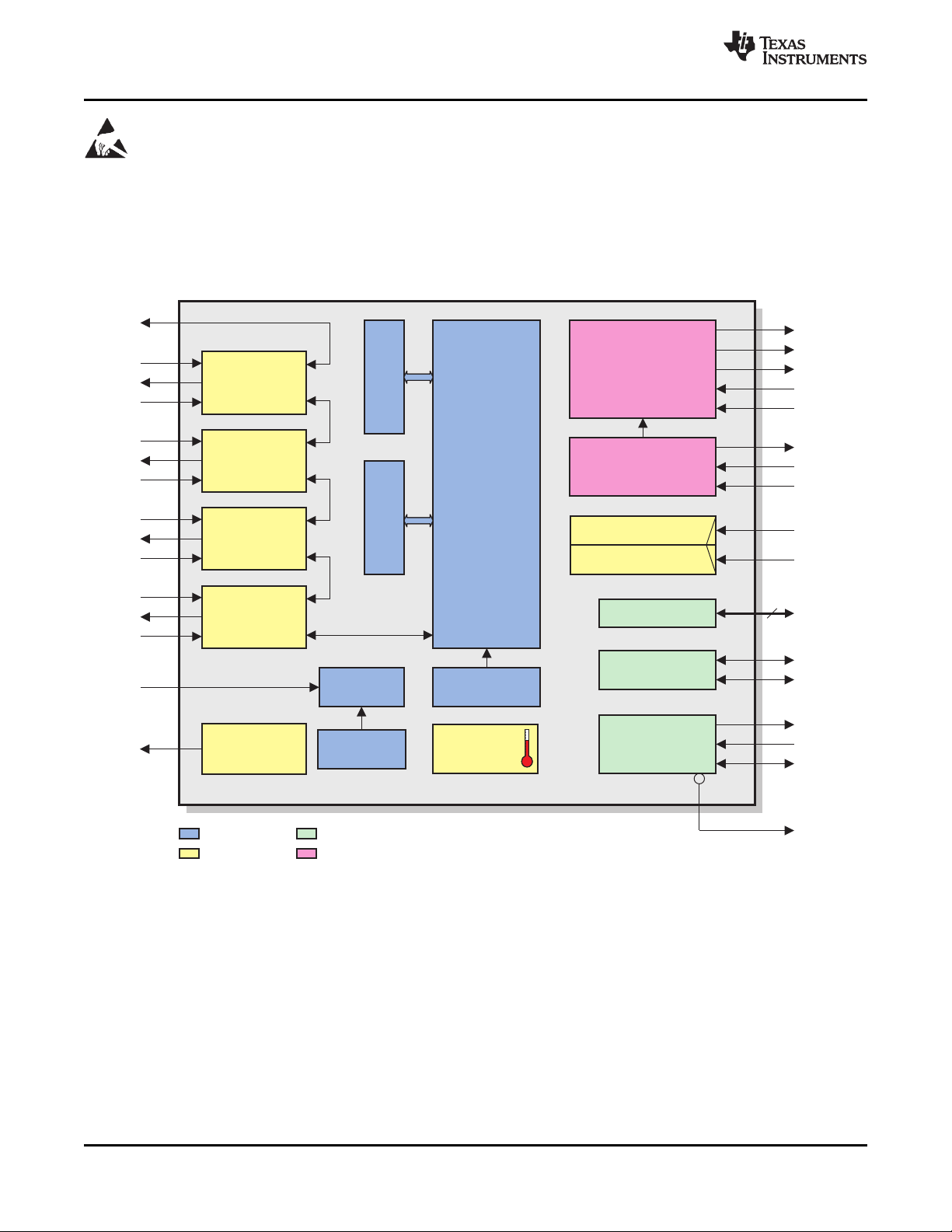
DESCRIPTION (CONTINUED)
The bq78PL114 is completely user-configurable, with parametric tables in flash memory to suit a variety of cell
chemistries, operating conditions, safety controls, and data reporting needs. It is easily configured using the
supplied bqWizard™ graphical user interface (GUI). The device is fully programmed and requires no algorithm or
firmware development.
Figure 1. bq78PL114 Internal Block Diagram
2 Submit Documentation Feedback Copyright © 2008, Texas Instruments Incorporated
Product Folder Link(s): bq78PL114
Page 3
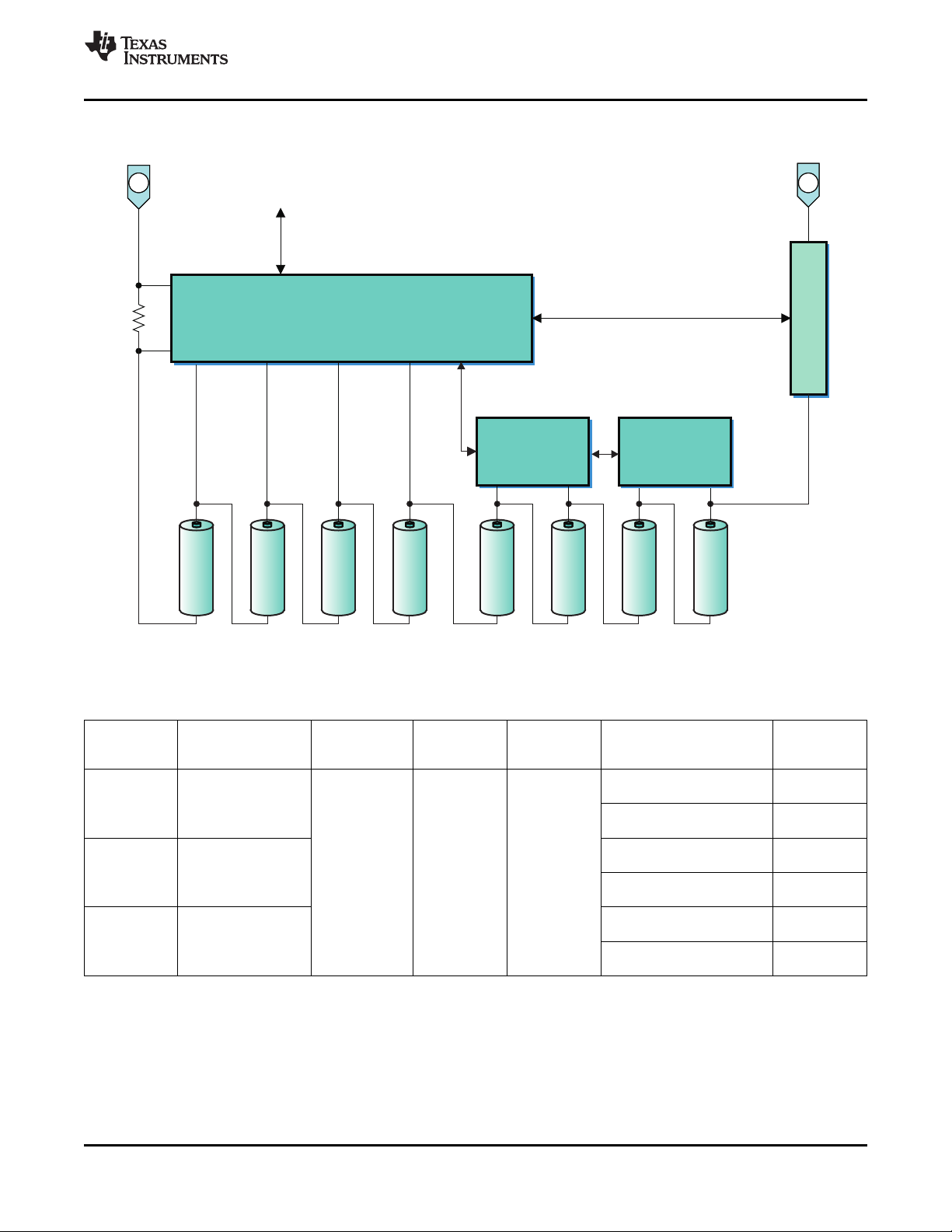
bq76PL102 Cell
MonitorWith
PowerPump
Balancing
PowerLAN
Communication
Link
PowerLAN
MasterGateway
BatteryController
bq78PL114
Pack
Positive
Pack
Negative
Example8-cellconfigurationshown
–
+
SMBus
R
SEN
SE
PackProtection
CircuitsandFuse
B0332-01
bq76PL102 Cell
MonitorWith
PowerPump
Balancing
bq78PL114
www.ti.com
.................................................................................................................................... SLUS850A – SEPTEMBER 2008 – REVISED SEPTEMBER 2008
Figure 2. Example PowerLAN Multicell System Implementation
ORDERING INFORMATION
Product Cell Configuration
(2)
Package Ordering Number Transport
bq78PL114 3 to 8 series cells
bq78PL114 QFN-48, 7-mm
(PREVIEW) × 7-mm
3 to 10 series cells RGZ – 40 ° C to 85 ° C
bq78PL114
(PREVIEW)
3 to 12 series cells
(1) Authentication options are also available; contact TI for additional information.
(2) For configurations consisting of more than four series cells, additional bq76PL102 parts must be used.
(3) Some historical data storage limits exist for the S10 and S12 versions.
Package Temperature
Designator Range
(1)
Quantity,
Media
bq78PL114RGZT
bq78PL114RGZR
bq78PL114S10RGZT
bq78PL114S10RGZR
bq78PL114S12RGZT
bq78PL114S12RGZR
(3)
(3)
(3)
(3)
250, tape and
reel
2500, tape and
reel
250, tape and
reel
2500, tape and
reel
250, tape and
reel
2500, tape and
reel
Copyright © 2008, Texas Instruments Incorporated Submit Documentation Feedback 3
Product Folder Link(s): bq78PL114
Page 4
P0023-16
bq78PL114
RGZPackage
(TopView)
CHG
SDO0
DSG
SDI1
PRE
P1N
EFCIC
P2S
EFCID
P2N
CCBAT
SDO2
CCPACK
SDI3
VLDO1
P3S
CSBAT
P3N
CSPACK
P4S
OSCI
P4N
OSCO
P-LAN
1
2
3
4
5
6
7
8
9
10
11
12
13
14
15
16
17
18
19
20
21
22
23
24
LED5
VSS
LED4
V1
LED3
XT1
LED2
XT2
LED1
V2
LEDEN
VLDO2
SPROT
V3
SELECT
XT3
SPI-DO
XT4
SPI-DI
V4
SPI-CLK
SMBDAT
RSTN
SMBCLK
36
35
34
33
32
31
30
29
28
27
26
25
48
47
46
45
44
43
42
41
40
39
38
37
ThermalPad
bq78PL114
SLUS850A – SEPTEMBER 2008 – REVISED SEPTEMBER 2008 ....................................................................................................................................
AVAILABLE OPTIONS
www.ti.com
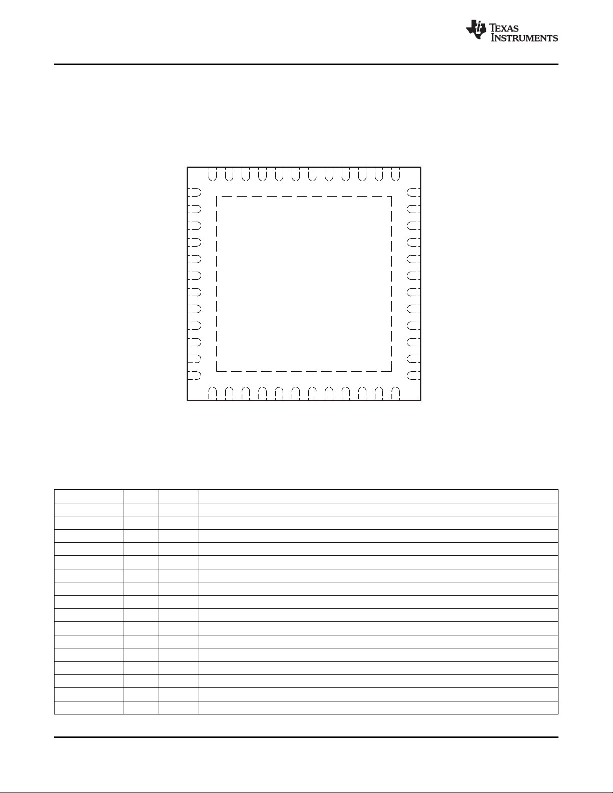
Figure 3. bq78PL114 Pinout
(1)
NAME NO. TYPE
CCBAT 6 IA Coulomb counter input (sense resistor), connect to battery negative
CCPACK 7 IA Coulomb counter input (sense resistor), connect to pack negative
CHG 1 O Charge MOSFET control (active-high, enables current flow)
CSBAT 9 IA Current sense input (safety), connect to battery negative
CSPACK 10 IA Current sense input (safety), connect to pack negative
DSG 2 O Discharge MOSFET control (active-high, low opens MOSFET)
EFCIC 4 I External charge MOSFET control input
EFCID 5 I External discharge MOSFET control input
LED1 32 IO LED1 – active-low
LED2 33 IO LED2 – active-low
LED3 34 IO LED3 – active-low
LED4 35 IO LED4 – active-low
LED5 36 IO LED5 – active-low
LEDEN 31 IO LEDEN – common-anode drive (active-high)
OSCI 11 I External oscillator input (optional)
OSCO 12 O External oscillator output (optional)
(1) I – input, IA – analog input, O – output, OA – analog output, P – power
4 Submit Documentation Feedback Copyright © 2008, Texas Instruments Incorporated
TERMINAL FUNCTIONS
DESCRIPTION
Product Folder Link(s): bq78PL114
Page 5

bq78PL114
www.ti.com
.................................................................................................................................... SLUS850A – SEPTEMBER 2008 – REVISED SEPTEMBER 2008
TERMINAL FUNCTIONS (continued)
NAME NO. TYPE
P1N 15 O Charge-balance gate drive, cell 1 north
P2S 16 O Charge-balance gate drive, cell 2 south
P2N 17 O Charge-balance gate drive, cell 2 north
P3N 21 O Charge-balance gate drive, cell 3 north
P3S 20 O Charge-balance gate drive, cell 3 south
P4N 23 O Charge-balance gate drive, cell 4 north
P4S 22 O Charge-balance gate drive, cell 4 south
P-LAN 24 IO PowerLAN I/O to external bq76PL10x nodes
PRE 3 O Pre-Charge MOSFET control (active-high.)
RSTN 25 I Device reset, active-low
SDI1 14 I Connect to SDO0 via a capacitor
SDI3 19 I Internal PowerLAN connection – connect to SDO2
SDO0 13 O Requires 100-k Ω pullup resistor to VLDO1
SDO2 18 O Internal PowerLAN connection – connect to SDI3
SELECT 29 O Auxiliary SPI control output
SMBCLK 37 IO SMBus clock signal
SMBDAT 38 IO SMBus data signal
SPI-CLK 26 IO SPI port clock
SPI-DI 27 I SPI master-out-slave-in
SPI-DO 28 O SPI master-in-slave-out
SPROT 30 O Secondary protection output, active-high (FUSE)
V1 47 IA Cell-1 positive input
V2 44 IA Cell-2 positive input
V3 42 IA Cell-3 positive input
V4 39 IA Cell-4 positive input
VLDO1 8 P Internal LDO-1 output, bypass with capacitor
VLDO2 43 P Internal LDO-2 output, bypass with capacitor
VSS 48 IA Cell-1 negative input
XT1 46 IA External temperature-sensor-1 input
XT2 45 IA External temperature-sensor-2 input
XT3 41 IA External temperature-sensor-3 input
XT4 40 IA External temperature-sensor-4 input
– – P Thermal pad. Connect to VSS
(2) SPI functionality requires a firmware option, consult the factory for additional information.
(1)
(2)
(2)
(2)
(2)
DESCRIPTION
Copyright © 2008, Texas Instruments Incorporated Submit Documentation Feedback 5
Product Folder Link(s): bq78PL114
Page 6

bq78PL114
SLUS850A – SEPTEMBER 2008 – REVISED SEPTEMBER 2008 ....................................................................................................................................
ABSOLUTE MAXIMUM RATINGS
(1)
www.ti.com
over operating free-air temperature range (unless otherwise noted)
RANGE UNITS
T
A
T
stg
V4 – V3 Maximum cell voltage – 0.5 to 5.0 V
V3 – V2 Maximum cell voltage – 0.5 to 5.0 V
V2 – V1 Maximum cell voltage – 0.5 to 5.0 V
V1 – VSS Maximum cell voltage – 0.5 to 5.0 V
Voltage on LED1 – LED5, CCBAT,
CCPACK, CSBAT, CSPACK, XT1, XT2,
OSCI, OSCO, SDIx, SDOx, SPROT,
P-LAN
Voltage on XT3, XT4, LEDEN Maximum voltage range V
EFCIC, EFCID With respect to VSS – 0.5 to 5.5 V
Voltage on SMBCLK, SMBDAT With respect to VSS – 0.5 to 6 V
Voltage on PRE, CHG, DSG With respect to VSS – 0.5 to (VLDO1 + 0.5) V
Current through PRE, CHG, DSG,
LED1 – LED5, P-LAN
VLDO1 maximum current Maximum current draw from VLDO 20 mA
ESD tolerance 2 kV
Lead temperature, soldering Total time < 3 seconds 300 ° C
(1) Stresses beyond those listed under Absolute Maximum Ratings may cause permanent damage to the device. These are stress ratings
only, and functional operation of the device at these or any other conditions beyond those indicated under Recommended Operating
Conditions is not implied. Exposure to absolute-maximum-rated conditions for extended periods may affect device reliability.
Operating free-air temperature (ambient) – 40 to 85 ° C
Storage temperature – 65 to 150 ° C
Maximum voltage on any I/O pin V
Maximum current source/sink 20 mA
JEDEC, JESD22-A114 human-body model, R = 1500 Ω , C =
100 pF
(VSS – 0.5) to
(VLDO1 + 0.5)
(V2 – 0.5) to
(VLDO2 + 0.5)
6 Submit Documentation Feedback Copyright © 2008, Texas Instruments Incorporated
Product Folder Link(s): bq78PL114
Page 7
bq78PL114
www.ti.com
.................................................................................................................................... SLUS850A – SEPTEMBER 2008 – REVISED SEPTEMBER 2008
ELECTRICAL CHARACTERISTICS
TA= – 40 ° C to 85 ° C (unless otherwise noted)
DC Characteristics
PARAMETER TEST CONDITIONS MIN TYP MAX UNIT
(1)
V
CELL
I
DD
I
STBY
I
SHIP
I
ECUV
V
OL
V
OH
V
IL
V
IH
Operating range Cells balanced 2.3 4.5 V
Operating-mode current Measure / report state 250 µ A
Standby-mode current SMBCLK = SMBDAT = L 100 µ A
Ship-mode current 30 µ A
Extreme cell under voltage All cells < 2.7 V and any cell < ECUV set
shutdown current point
General I/O pins IOL< 4 mA 0 0.5 V
(2)
General I/O pins IOH< – 4 mA V
– 0.1 V
LDO1
General I/O pins 0.25 V
General I/O pins 0.75 V
LDO1
1 µ A
LDO1
(1) Device remains operational to 1.85 V with reduced accuracy and performancce.
(2) Does not apply to SMBus pins.
Voltage-Measurement Characteristics
over operating free-air temperature range (unless otherwise noted)
PARAMETER TEST CONDITIONS MIN TYP MAX UNIT
Measurement range 2.5 4.5 V
Resolution < 1 mV
Accuracy mV
25 ° C ± 5
0 ° C to 60 ° C ± 10
V
V
Current-Sense Characteristics
over operating free-air temperature range (unless otherwise noted)
PARAMETER TEST CONDITIONS MIN TYP MAX UNIT
Measurement range
Input offset TA= 25 ° C ± 50 µ V
Offset drift TA= 0 ° C to 60 ° C 0.5 µ V/ ° C
Resolution 18 µ V
Full-scale error
Full-scale error drift TA= 0 ° C to 60 ° C 50 PPM/ ° C
(1) Default range. Corresponds to ± 10 A using a 10-m Ω sense resistor. Other gains and ranges are available (eight options).
(2) After calibration. Accuracy is dependent on system calibration and temperature coefficient of sense resistor.
Coulomb-Counter Characteristics
over operating free-air temperature range (unless otherwise noted)
Resolution 5 nVh
Intergral nonlinearity 0.008%
Snap-to-zero (deadband) ± 100
(1) Shares common input with Current Sense section
(2) After calibration. Accuracy is dependent on system calibration and temperature coefficient of sense resistor.
(3) Corresponds to 20 mA using 5-m Ω sense resistor
(1)
(2)
TA= 25 ° C ± 0.1%
(1) (2)
– 0.2 0.2 V
PARAMETER TEST CONDITIONS MIN TYP MAX UNIT
(3)
µ V
Copyright © 2008, Texas Instruments Incorporated Submit Documentation Feedback 7
Product Folder Link(s): bq78PL114
Page 8

bq78PL114
SLUS850A – SEPTEMBER 2008 – REVISED SEPTEMBER 2008 ....................................................................................................................................
Current-Sense (Safety) Characteristics
(1)
www.ti.com
over operating free-air temperature range (unless otherwise noted)
PARAMETER TEST CONDITIONS MIN TYP MAX UNIT
Measurement range – 0.312 0.312 V
Resolution mV
Short-circuit detection 10
Overcurrent detection, charge and discharge 1.25
(1) Post calibration: Dependent on system calibration and temperature coefficient of sense resistor. Uncertainty 1.5 LSB.
Internal Temperature-Sensor Characteristics
(1)
over operating free-air temperature range (unless otherwise noted)
PARAMETER TEST CONDITIONS MIN TYP MAX UNIT
Measurement range – 30 85 ° C
Resolution 0.1 ° C
Accuracy
(1)
– 30 ° to 85 ° ± 1 ° C
(1) After calibration.
External Temperature-Sensor(s) Typical Characteristics
(1)
over operating free-air temperature range (unless otherwise noted)
PARAMETER TEST CONDITIONS MIN TYP MAX UNIT
Measurement range
Resolution 0.2 ° C
Accuracy
(3)
(1) Typical for dual diode (MMBD4148 or equivalent) external sensor using recommended circuit.
(2) Range of diode sensors may exceed operational limits of IC and battery cells.
(3) Typical behavior after calibration, final result dependent on specific component characteristics.
(2)
– 40 90 ° C
25 ° ± 1
0 ° to 85 ° ± 2
° C
SMBus Characteristics
(1)
over operating free-air temperature range (unless otherwise noted)
PARAMETER TEST CONDITIONS MIN TYP MAX UNIT
V
IL
V
IH
V
OL
C
I
f
SCL
(2)
R
PU
(1) SMBus timing and signals meet the SMBus 2.0 specification requirements under normal operating conditions. All signals are measured
with respect to PACK-negative.
(2) Pullups are typically implemented external to battery pack, and are selected to meet SMBus requirements.
Input low voltage 0 0.8 V
Input high voltage 2.1 5.5 V
Output low voltage 350- µ A sink current 0 0.4 V
Capacitance, each I/O pin 10 pF
SCLK nominal clock frequency TA= 25 ° C 100 kHz
V
5 V nominal 13.3 45.3
Pullup resistors for SCLK, SDATA k Ω
BUS
V
3 V nominal 2.4 6.8
BUS
8 Submit Documentation Feedback Copyright © 2008, Texas Instruments Incorporated
Product Folder Link(s): bq78PL114
Page 9

bq78PL114
PowerLAN
GatewayBattery
Management
Controller
R
PRE
+
PACK+
–
SPI-DI
SMBCLK
SMBDAT
R
SENSE
PACK–
XT1–XT4
Temperature
Sensor(typ.)
SPROT
LED1–LED5
Typicalsix-cellconfigurationshown.
AdditionalcellsaddedviaPowerLANconnection.
Somecomponentsomittedforclarity.
SPI-DO
V2
V3
V4
V1
VLDO2
C
RFI
VLDO1
RSTN
SDO2
SDI3
EFCID
EFCIC
Oneof4external
sensorsshown
SPI-CLK
P-LAN
5
CELL 6
CELL 5
V2
V1
SDI1
SDO0
SELECT
Level-ShiftCircuits
CHG
DSG
PRE
ESDProtection
SMBus
SPI
AuxFET
Control
ThermalPad
VSS
CSBAT
CCBAT
CCPACK
CSP
ACK
CellBalancing
Circuits
CellBalancingCircuits
bq76PL102
CELL 4
CELL 3
CELL 2
CELL 1
S0342-02
bq78PL114
www.ti.com
.................................................................................................................................... SLUS850A – SEPTEMBER 2008 – REVISED SEPTEMBER 2008
Figure 4. bq78PL114 Simplified Example Circuit Diagram
Copyright © 2008, Texas Instruments Incorporated Submit Documentation Feedback 9
Product Folder Link(s): bq78PL114
Page 10

bq78PL114
SLUS850A – SEPTEMBER 2008 – REVISED SEPTEMBER 2008 ....................................................................................................................................
www.ti.com
FEATURE SET
Primary (First-Level) Safety Features
The bq78PL114 implements a breadth of system protection features which are easily configured by the
customer. First-level protections work by controlling the MOSFET switches. These include:
• Battery cell over/undervoltage protection
• Pack over/undervoltage protection
• Charge and discharge overcurrent protection
• Short-circuit protection
• External MOSFET control inputs (EFCIx) with programmable polarity
• Up to four external temperature inputs for accurate cell and MOSFET monitoring
• Watchdog timer protection
• Brownout detection and protection against extreme pack undervoltage
Secondary (Second-Level) Safety Features
The bq78PL114 can detect more serious system faults and activate the SPROT pin, which can be used to open
an in-line chemical fuse to permanently disable the pack. Secondary optional features include
• Fully independent of first-level protections
• SmartSafety algorithms for early detection of potential faults
– Temperature abnormalities (variances, extremes, rate of change, etc.)
– Disconnected cell voltage inputs
– Cell imbalance exceeds safety limits
– Impedance rise due to cell or weld strap fault
• MOSFET failure or loss of MOSFET control
• Safety overvoltage, pack and cell
• Safety overtemperature, limits for both charge and discharge
• Safety overcurrent, charge and discharge
• Failed current measurement, voltage measurement, or temperature measurement
Charge Control Features
• Meets SMBus 2.0 and Smart Battery System (SBS) Specification 1.1 requirements
• Active cell balancing using patented PowerPump technology, which eliminates unrecoverable capacity loss
due to normal cell imbalance
• Balancing-current monitoring to detect cell problems
• Simultaneous, synchronous measurement of all cell voltages in a pack
• Simultaneous, synchronous measurement of pack current with cell voltages
• Reports target charging current and/or voltage to an SBS Smart Charger
• Reports the chemical state-of-charge for each cell and pack
• Supports precharging and zero-volt charging with separate MOSFET control
• Programmable, Chemistry-specific parameters
• Fault reporting
Gas Gauging
• The bq78PL114 accurately reports battery cell and pack state-of-charge (SOC). No full charge/discharge
cycle is required for accurate reporting.
• State-of-charge is reported via SMBus and optional LED display.
• 18-bit integrating delta-sigma ADC coulomb counter, with programmable snap-to-zero value
LED Display
• The bq78PL114 drives a three- to five-egment LED display in response to a pushbutton (LEDEN) input signal.
Each LED pin can sink up to 10 mA.
10 Submit Documentation Feedback Copyright © 2008, Texas Instruments Incorporated
Product Folder Link(s): bq78PL114
Page 11

bq78PL114
www.ti.com
.................................................................................................................................... SLUS850A – SEPTEMBER 2008 – REVISED SEPTEMBER 2008
Lifetime Data Logging (Readable via SMBus or SPI)
• Recording of faults, events, anomalies, minimum and maximum values
• Maximum/minimum temperature
• Maximum/minimum pack voltage
• Maximum/minimum cell voltages
• Maximum charge and discharge currents
Forensic Data Logging (Readable via SMBus or SPI)
• Last known full capacity of each cell
• Cycle count and/or cumulative number of ampere-hours delivered by the battery
• Battery pack status: being charged, discharged, or at rest
• Balancing effort required by each bank of cells to maintain balance
• Information for each cell bank for period leading up to failure
• Last 10 failures causing first-level safety action
• Forensic data up-loadable to host CPU via SMBus or SPI
• Forensic data recording of anomalies and events
Power Modes
• Normal Mode: The bq78PL114 performs measurements and calculations, makes decisions, and updates
internal data approximately once per second. All safety circuitry is fully functional in this mode.
• Standby Mode: The bq78PL114 performs as in normal mode, but at a dramatically reduced rate to lower
power consumption at times when the host computer is inactive or the battery system is not being used. All
safety circuitry remains fully functional in this mode.
• Ship Mode: The bq78PL114 disables (opens) all the protection MOSFETs, and continues to monitor
temperature and voltage, but at a reduced measurement rate to dramatically lower power consumption.
Environmental data is saved in flash as a part of the historical record. Safety circuitry is disabled in this mode.
The device does not enter this power state as a part of normal operation; it is intended for use after factory
programming and test. Entry occurs only after a unique SMBus or SPI command is issued. Exit occurs when
the SMBus or SPI lines return to an active state.
• Extreme Cell Undervoltage (ECUV) Shutdown Mode: In this mode, the bq78PL114 draws minimal current
and the charge and discharge protection MOSFETs are disabled (opened). The precharge MOSFET remains
enabled when a charge voltage is present. Safety circuitry is disabled in this mode. The device does not enter
this mode as a part of normal operation; it enters this state during extreme cell undervoltage conditions
(ECUV). The ECUV threshold is fully programmable below 2.7V.
STATE ENTRY CONDITION EXIT CONDITION
Active < 250 µ A Fully active
Standby < 150 µ A Fully active Load activity
Ship < 40 µ A Not active Protected SMBus or SPI command SMBus or SPI becomes active
Extreme cell Vcell charge above ECUV recovery
undervoltage threshold (2.7 V/cell typical)
CURRENT OVERCURRENT
DRAW (Typ) PROTECTION
Normal operation as determined by Firmware directed to the following
firmware operating modes
No load current flowing for
predetermined time
Not active
< 1 µ A (precharge Enabled when Vcell < ECUV
enabled)
OPERATION
The bq78PL114 battery management controller serves as the master controller for a Li-Ion battery system
consisting of up to 12 cells in series. Any number may be connected in parallel; other system or safety issues
limit the number of parallel cells. The bq78PL114 provides extraordinarily precise state-of-charge gas gauging
along with first and second level pack safety functions. Voltage and current measurements are performed
synchronously and simultaneously for all cells in the system, allowing a level of precision not previously possible
Copyright © 2008, Texas Instruments Incorporated Submit Documentation Feedback 11
Product Folder Link(s): bq78PL114
Page 12

bq78PL114
SLUS850A – SEPTEMBER 2008 – REVISED SEPTEMBER 2008 ....................................................................................................................................
www.ti.com
in battery management. Temperature is measured by up to four additional external temperature sensors, for a
total of five independent measurement points. (Additional cell temperature sensors are available in remote
bq76PL102 dual-cell battery monitors.) Coulomb counting is captured continuously by a dedicated 18-bit
integrating delta-sigma ADC in the bq78PL114. The CPU in the bq78PL114 is also responsible for system data
calculations, black-box forensic data storage, and communicating parameters via the SMBus or SPI interface.
PowerLAN Communication Link
PowerLAN technology is Texas Instruments ’ patented serial network and protocol designed specifically for
battery management in a multicell system environment. The PowerLAN link is used to initiate and report
measurements of cell voltage and temperature, and control cell balancing. The bq78PL114 serves as the master
controller of the PowerLAN link and can interface to multiple bq76PL102 dual-cell battery monitors, which
measure and balance additional cells. The bq78PL114 monitors the first three or four cells, and bq76PL102s can
be added to monitor more series cells.
The PowerLAN link isolates voltages from adjacent bq76PL102 devices to permit high-voltage stack assembly
without compromising precision and accuracy. The PowerLAN link is expandable to support up to 12 cells in
series. Each bq76PL102 handles voltage and temperature measurements, as well as balancing for two cells. The
PowerLAN link provides high ESD tolerance and high immunity to noise generated by nearby digital circuitry or
switching currents. Each bq76PL102 has both a PowerLAN input and PowerLAN output: Received data is
buffered and retransmitted, permitting high numbers of nodes without loss of signal fidelity. Signals are
capacitor-coupled between nodes, providing dc isolation.
Safety
Unique in the battery-management controller market, the bq78PL114 simultaneously measures voltage and
current using independent and highly accurate delta-sigma ADCs. This technique removes virtually all systemic
noise from measurements, which are made during all modes of battery operation: charge, discharge, and rest.
The bq78PL114 also directs all connected bq76PL102 dual-cell battery monitors to measure each cell voltage
simultaneously with the bq78PL114 measurements. Battery impedance and self-discharge characteristics are
thus measured with an unprecedented level of accuracy in real time. The bq78PL114 applies this precise
information to SmartSafety algorithms to detect certain anomalies and conditions which may be indicative of
internal cell faults, before they become serious problems.
The bq78PL114 uses its enhanced measurement system to detect system faults including cell under- and
overvoltage, cell under- and overtemperature, system overvoltage, and system overcurrent. First-level safety
algorithms first attempt to open the MOSFET safety switches. If this fails, second-level safety algorithms activate
the SPROT output, normally used to open a fuse and provide permanent, hard protection for the systems.
External MOSFET control inputs with programmable polarity can also be used to operate the safety MOSFETs
under control of user supplied circuitry. The bq78PL114 continuously monitors these inputs. If any MOSFET fails
to open when commanded; the 2
nd
level safety algorithms also activate the SPROT output. All first- and
second-level safety algorithms have fully programmable time delays to prevent false triggering.
Cell Balancing
Patented PowerPump cell balancing technology drastically increases the useful life of battery packs by
eliminating the cycle life fade of multi-cell packs due to cell imbalance. PowerPump technology efficiently
transfers charge from cell to cell, rather than simply bleeding off charging energy as heat as is typically done with
resistive-bleed balancing circuits. Balancing is configurable and may be performed during any battery operational
modes: charge, discharge, or rest. Compared to resistive bleed balancing, virtually no energy is lost as heat. The
actual balance current is externally scalable and can range from 10 mA to 1 A (100 mA typical) depending on
component selection and system or cell requirements.
A variety of techniques, such as simple terminal voltage, terminal voltage corrected for impedance and
temperature effects, or state-of-charge balancing, is easily implemented by the bq78PL114. In some cases,
chemistry-specific algorithms are available. By tracking the balancing required by individual cells, overall battery
safety is enhanced, often allowing early detection of soft shorts or other cell failures. Balancing is achieved
between all cells within the pack as dynamically determined by the bq78PL114.
12 Submit Documentation Feedback Copyright © 2008, Texas Instruments Incorporated
Product Folder Link(s): bq78PL114
Page 13

bq78PL114
www.ti.com
.................................................................................................................................... SLUS850A – SEPTEMBER 2008 – REVISED SEPTEMBER 2008
Outputs
Charge Control
The CHG and PRE outputs are ordinarily used to drive MOSFET transistors controlling charge to the cell stack.
Charge or precharge mode is selected based on the present cell voltage compared to the user-definable cell
precharge, undervoltage, and temperature thresholds. When below these limits, the PRE signal is active and the
CHG signal is inactive. This turns on the precharge MOSFET and is used to charge a depleted system through a
current-limiting series resistor. When all cell voltages are above the limit and the temperature is above the charge
temperature minimum, then the CHG output also becomes active and enables the charge MOSFET to turn on,
providing a high-current path between charger and battery cells.
The CHG and PRE MOSFET control outputs are both disabled (low) when any cell reaches the safety cutoff limit
or temperature threshold. During active charging modes (and above cell voltage thresholds), the discharge
MOSFET is also enabled to avoid excessive heating of the body diode. Similarly, the charge MOSFET is active
during discharge, provided current flow is in the correct direction and no safety violations are present.
The CHG and PRE outputs are intended to drive buffer transistors acting as inverting level shifters.
Discharge Control
The DSG output operates similarly to control-system discharging. It is enabled (high) by default. If a cell voltage
falls below a programmable threshold, or excessive current or other safety related fault is sensed, the DSG
output is disabled (low) to prevent damage to the cells.
All facets of safely charging and discharging the cell stack are controlled by user-definable parameters which
provide precise control over MOSFET states. Both system and cell over- and undervoltage limits are provided, as
well as programmable hysteresis to prevent oscillation. Temperature and current thresholds are also provided,
each with independent timers to prevent nuisance activations.
LEDEN
LEDEN is a dual-function pin. One function is to provide output current to the LED display array. It also serves as
an input that monitors for closure of a state-of-charge indicator (SOCi) push-button switch.
LED SOCi Outputs
LED1 – LED5 are current-sinking outputs designed to drive low-current LEDs. The LEDs can be activated by the
LEDEN pin via a pushbutton switch. They can be configured (using SBS parameters) to operate in bar or dot
mode and to use three to five LEDs to represent state-of-charge information.
Inputs
Current Measurement
Current is monitored by four separate ADCs. All use the same very low-value sense resistor, typically either 5 or
10 milliohms in series with the pack negative connection. CCBAT and CCPACK connections to the sense
resistor use an R/C filter for noise reduction. (CSBAT and CSPACK are direct connections used for secondary
safety.) It is possible to use even lower values for the sense resistor in very high-current designs by employing
external circuitry. Contact Texas Instruments directly for details.
A 14-bit delta-sigma ADC is used to measure current flow accurately in both directions. The measurements are
taken simultaneously and synchronously with all the cell voltage measurements, even those cells measured by
bq76PL102 dual-cell battery monitors.
Coulomb Counting
A dedicated coulomb counter is used to measure charge flow with 18 bit precision in both directions by a
calibrated, integrating delta-sigma ADC. This allows the bq78PL114 to keep very accurate state-of-charge (SOC)
information and battery statistics. A small deadband is applied to further reduce noise effects. The coulomb
counter is unique in that it continues to accumulate (integrate) current flow in either direction even as the rest of
the internal microcontroller is placed in a very low power state, further lowering power consumption without
compromising system accuracy.
Copyright © 2008, Texas Instruments Incorporated Submit Documentation Feedback 13
Product Folder Link(s): bq78PL114
Page 14

bq78PL114
SLUS850A – SEPTEMBER 2008 – REVISED SEPTEMBER 2008 ....................................................................................................................................
www.ti.com
Safety Current
Two additional ADCs are used to directly monitor for overcurrent or short-circuit current conditions, independently
of the internal function. This provides a direct and rapid response to insure pack integrity and safe operation by
opening the appropriate MOSFETs. These functions are implemented in hardware, and do not require firmware
for functionality.
Voltage Measurement
Voltage measurement is performed by four independent delta-sigma ADCs which operate simultaneously and
are triggered synchronously so that all voltages are read at precisely the same moment. The bq78PL114
coordinates the attached bq76PL102 dual-cell battery monitors so they also perform their cell voltage
measurements in sync with the bq78PL114 voltage and current measurements. Voltage measurements are
converted with better than 1 mV of resolution, providing superior accuracy. One-ADC-per-cell technology means
that voltage is also measured simultaneously with current, permitting accurate, real-time cell impedance
calculation during all operating conditions. This technique also provides greatly enhanced noise immunity and
filtering of the input signal without signal loss.
Temperature Measurement
XT1 – XT4 are dedicated temperature inputs. Each external sensor consists of a low-cost silicon diode (dual diode
in one package is recommended) and capacitor combination. XT1, multiplexed with the LED1 and LED2 inputs,
is used to measure cells 1 and 3. XT2, multiplexed with the LED1 and LED2 inputs, is used to measure cells 2
and 4. XT3 is a dedicated IC-temperature sensor, which should be placed near the bq78PL114 IC. XT4 is
dedicated to protection-MOSFET temperature and governed by safety rules. The sensor attached to XT4 should
be placed near the pack-disconnect MOSFETs. Temperatures for cells 5 and above are measured by external
bq76PL102(s), and the temperature data is received by the bq78PL114 over the PowerLAN link for processing.
The bq78PL114 can report all of these temperatures individually and as an average. A single internal, integrated
silicon sensor is also supplied in the bq78PL114.
Note that additional external temperature sensors can be added using bq76PL102 dual-cell battery monitors
operating on the PowerLAN link. Each bq76PL102 contains one internal temperature monitor and two additional
external temperature-sensor inputs (in addition to the two cell-voltage measurements and cell balancing).
EFCIx
The external MOSFET control inputs are for user control of MOSFETs based on external circuitry and conditions.
The polarity of the input signal is user programmable. Two modes of operation are possible. The first mode is
used to implement additional hardware safety inputs, and is used to force the protection MOSFETs to an OFF
state. The polarity of the input signals is programmable. The inputs can also be used to control the MOSFETs
directly through hardware, with no firmware operation required.
COMMUNICATIONS
SMBus
The bq78PL114 uses the industry-standard Smart Battery System ’ s two-wire System Management Bus (SMBus)
communications protocol for all external communication. SMBus version 2.0 is supported by the bq78PL114, and
includes clock stretching, bus fault time-out detection, and optional packet error checking (PEC). For additional
information, see the www.smbus.org and www.sbs-forum.org Web sites.
SPI
The bq78PL114 provides a standard serial peripheral interface (SPI) port consisting of SELECT, SPI-DI, SPI-DO,
and SPI-CLK signals. This port may be operated as a master or slave SPI port. A typical system configuration
uses the bq78PL114 as a SPI slave device so that a host controller could access the various battery data using
the industry-standard Smart Battery Data specification for content.
Alternatively, the SPI port may be operated as a master to allow the bq78PL114 to write selected system data to
another device for use in an autonomous application.
Contact Texas Instruments for additional SPI options and details.
14 Submit Documentation Feedback Copyright © 2008, Texas Instruments Incorporated
Product Folder Link(s): bq78PL114
Page 15

bq78PL114
www.ti.com
.................................................................................................................................... SLUS850A – SEPTEMBER 2008 – REVISED SEPTEMBER 2008
Smart Battery Data (SBData)
The data content and formatting of the bq78PL114 information conforms to the Smart Battery System ’ s (SBS)
Smart Battery Data specification, version 1.1. See the SBS/SMBus site at www.sbs-forum.com for further
information regarding these specifications.
This SBS Data (SBData) specification defines read/write commands for accessing data commonly required in
laptop computer applications. The commands are generic enough to be useful in most applications.
Because the bq78PL114 provides a wealth of control and battery information beyond the SBData standard, new
command codes have been defined by Texas Instruments. In addition, new battery data features, such as
state-of-health, use newly defined extended SBData command codes. Standard SMBus protocols are used,
although additional data values beyond those defined by the Smart Battery Data specification are employed. (For
example, the bq78PL114 typically is used in a multicell battery system and may report individual cell voltages for
up to 12 cells. The SBData command set only defines four cell-voltage registers.)
Copyright © 2008, Texas Instruments Incorporated Submit Documentation Feedback 15
Product Folder Link(s): bq78PL114
Page 16

bq78PL114
SLUS850A – SEPTEMBER 2008 – REVISED SEPTEMBER 2008 ....................................................................................................................................
SBS Standard Data Parameter List (Abridged)
Command Data Type Descripotion
00 R/W word (unsigned) Manufacturer Access
01 R/W word (unsigned) Remaining Capacity Alarm Level
02 R/W word (unsigned) Remaining Time Alarm Level
03 R/W word (unsigned) Battery Mode
04 R/W word (unsigned) At Rate value used in AtRate calculations
05 Read word (unsigned) At Rate Time to Full
06 Read word (unsigned) At Rate Time to Empty
07 Read word (Boolean) At Rate OK
08 Read word (unsigned) Pack Temperature (maximum of all individual cells)
09 Read word (unsigned) Pack Voltage (sum of individual cell readings)
0A Read word (unsigned) Pack Current
0B Read word (unsigned) Average Pack Current
0C Read word (unsigned) Max Error
0D Read word (unsigned) Relative State of Charge
0E Read word (unsigned) Absolute State of Charge
0F Read word (unsigned) Remaining Pack Capacity
10 Read word (unsigned) Full Charge Capacity
11 Read word (unsigned) Run Time to Empty
12 Read word (unsigned) Average Time to Empty
13 Read word (unsigned) Average Time to Full
14 Read word (unsigned) Charging Current
15 Read word (unsigned) Charging Voltage
16 Read word (unsigned) Battery Status
17 Read word (unsigned) Cycle Count
18 Read word (unsigned) Design Capacity
19 Read word (unsigned) Design Voltage
1A Read word (unsigned) Specification Information
1B Read word (unsigned) Manufacture Date
1C Read word (unsigned) Serial Number
1D – 1F Reserved
20 Read block (string) Pack Manufacturer Name (31 characters maximum)
21 Read block (string) Pack Device Name (31 characters maximum)
22 Read block (string) Pack Chemistry
23 Read block (string) Manufacturer Data
24 – 2E Reserved
2F R/W Block Optional Manufacturer Function 5
30 – 3B Reserved
3C R/W word (unsigned) Optional Manufacturer Function 4 (Vcell 4)
3D R/W word (unsigned) Optional Manufacturer Function 3 (Vcell 3)
3E R/W word (unsigned) Optional Manufacturer Function 2 (Vcell 2)
3F R/W word (unsigned) Optional Manufacturer Function 1 (Vcell 1)
40 – 45 Unused
46 – 47 Reserved
48 – 4F Unused
50 – 55 Reserved
(1) (2)
www.ti.com
(1) Parameters 0x00 – 0x3F are compatible with the SBDATA specification.
(2) By default, the bq78PL114 initially responds to the SBData slave address < 0001 011R/W > (0x16, 0x17).
16 Submit Documentation Feedback Copyright © 2008, Texas Instruments Incorporated
Product Folder Link(s): bq78PL114
Page 17

bq78PL114
www.ti.com
Command Data Type Descripotion
56 – 57 Unused
58 – 5A Reserved
5B – 5F Unused
60 – 62 Reserved
63 – 6F Unused
70 Reserved
71 – FF Unused
.................................................................................................................................... SLUS850A – SEPTEMBER 2008 – REVISED SEPTEMBER 2008
Copyright © 2008, Texas Instruments Incorporated Submit Documentation Feedback 17
Product Folder Link(s): bq78PL114
Page 18

equival
ent
resistance
UsedforSafetyEv
ents
UsedforDeviceTemp.
T1=CELL1TEMP.
T2=CELL2TEMP.
T3=CELL3TEMP
.
TEMP-FET
S=FETTEMP.&USEDFORSAFETY.
TEMP-PCB=TEMP.OFU4
stargroundpointl
ocatedatR3
KeepthisconnectiontoBA
TT
-asshortandLowZaspossible.
1
CHG
2
DSG
3
PRE
4
EFCIC
5
EFCID
6
CCBAT
7
CCPACK
8
VLDO1
9
CSBAT
10
CSPACK
11
OSCI
12
OSCO
13
SDO0
14
SDI1
15
P1N
16
P2S
17
P2N
18
SDO2
19
SDI3
20
P3S
21
P3N
22
P4S
23
P4N
24
P-LAN
25
RSTN
26
SPI-CLK
27
SPI-DI
28
SPI-DO
29
SELECT
30
SPROT
31
LEDEN
32
LED1
33
LED2
34
LED3
35
LED4
36
LED5
37
SMBCLK
38
SMBDAT
39
V4
40
XT4
41
XT3
42
V3
43
VLDO2
44
V2
45
XT2
46
XT1
47
V1
48
VSS
49
TAB
U4
bq78PL114
C5
10uF
R44
10K
C38
0.1uF
C27
1000pF
C28
10uF
C43
0.1uF
C7
1.0uF
R5
100K
C11
1000pF
R28
4.7K
R27
4.7K
R49
100R
R50
100R
R54
100R
R55
100R
R43
1.0M
R51
1.0M
C40
1.0uF
C39
1.0uF
C41
1.0uF
R10
2K
R30
20K
R29
20K
C12
3300pF
C13
3300pF
Q1-A
FDC6327C
Q1-B
FDC6327C
L1
4.7uH
C30
22uF
D10
MA21D3800L
D9
MA21D3800L
1
2
3
4
SMBUS-PORT
R3
0.005R
R6
1.0M
Z1
5.6VDC
T3
MMBD4148SE
C6
1000pF
TEMP-PCB
MMBD4148SE
C45
1000pF
TEMP-FETS
MMBD4148SE
C46
1000pF
R9
2K
R11
20K
R12
20K
C14
3300pF
C15
3300pF
Q2-
A
FDC6327C
Q2-B
FDC6327C
L2
4.7uH
D5
MA21D3800L
D6
MA21D3800L
PACK+
PACK
-
D
S
G
Q11
MMBFJ201
Q12
BC846ALT1G
Vcebr=65V
R53
560K
R56
200K
ZR2
12.0VDC
BZT52C12-7-F
R58
30K
R59
1.0M
Q13
D
S
G
Q8
MMBFJ201
Q9
BC846ALT1G
Vcebr=65V
R40
560K
R41
200K
ZR1
12.0VDC
BZT52C12-7-F
R45
30K
R46
1.0M
Q10
C60
0.1uF
C61
0.1uF
Q15
BC846ALT1G
Vcebr=65V
R17
1.0M
R52
30K
R60
1.0M
Q16
R18
C1
22uF
C2
22uF
R19
1.0M
R25
1.0M
D23
D24
D25
D26
D27
S1
C3
1000pF
Q14
BSS138
C4
0.1uF
Q17
FDV304P
R1
100K
T1
MMBD4148SE
C8
1000pF
T2
MMBD4148SE
C16
1000pF
C42
0.1uF
C50
0.1uF
-
+
CELL1
-
+
CELL2
-
+
CELL3
VSS
VLDO1
VSS
VSS
VSS
VS
S
VLDO1
S001
bq78PL114
SLUS850A – SEPTEMBER 2008 – REVISED SEPTEMBER 2008 ....................................................................................................................................
REFERENCE SCHEMATIC (3 Series Cells)
www.ti.com
18 Submit Documentation Feedback Copyright © 2008, Texas Instruments Incorporated
Product Folder Link(s): bq78PL114
Page 19

equivalent
resistance
UsedforSafet
yEv
ents
UsedforDeviceTemp.
T1=CELL1TEMP.
T2=CELL2TEMP.
T3=CELL3TEMP.
T4=CELL4TEMP.
T5=CELL5TEMP
.
T6=CELL6TEMP.
T7=CELL7TEMP.
T8=CELL8TEMP.
TEMP-FETS=FETTEMP.&USEDFORSAFETY
.
TEMP-PCB=TEMP.OFU4
stargroundpoint
located
atR3
Keepthis connection toBATT
-asshortandLowZaspossibl
e.
1
CHG
2
DSG
3
PRE
4
EFCIC
5
EFCID
6
CCBAT
7
CCPACK
8
VLDO1
9
CSBAT
10
CSPACK
11
OSCI
12
OSCO
13
SDO0
14
SDI1
15
P1N
16
P2S
17
P2N
18
SDO2
19
SDI3
20
P3S
21
P3N
22
P4S
23
P4N
24
P-LAN
25
RSTN
26
SPI-CLK
27
SPI-DI
28
SPI-DO
29
SELECT
30
SPROT
31
LEDEN
32
LED1
33
LED2
34
LED3
35
LED4
36
LED5
37
SMBCLK
38
SMBDA
T
39
V4
40
XT4
41
XT3
42
V3
43
VLDO2
44
V2
45
XT2
46
XT1
47
V1
48
VSS
49
TAB
U4
bq78PL114
C5
10uF
R44
10K
C38
0.1uF
C27
1000pF
C28
10uF
C43
0.1uF
C7
1.0uF
R5
100K
C11
1000pF
R28
4.7K
R27
4.7K
R49
100R
R50
100R
C9
10uF
C10
1000pF
R54
100R
R55
100R
R43
1.0M
R51
1.0M
15
V1
12
V2
14
T1
13
T2
11
TMD
10
TCK
3
TDI
8
P2N
7
P2S
6
P1N
5
P1S
2
VLDO
16
VPP
9
SDO
4
SDI
17
TAB
1
VSS
U3
BQ76PL102
C40
1.0uF
C44
1.0uF
C39
1.0uF
C41
1.0uF
R10
2K
R30
20K
R29
20K
C12
3300pF
C13
3300pF
Q1-A
FDC6327C
Q1-B
FDC6327C
L1
4.7uH
C30
22uF
D10
MA21D3800L
D9
MA21D3800L
1
2
3
4
SMBUS-PORT
R3
0.005R
R6
1.0M
Z1
5.6VDC
T3
MMBD4148SE
C6
1000pF
T4
MMBD4148SE
C37
1000pF
TEMP-PCB
MMBD4148SE
C45
1000pF
TEMP-FETS
MMBD4148SE
C46
1000pF
R9
2K
R11
20K
R12
20K
C14
3300pF
C15
3300pF
Q2-A
FDC6327C
Q2-B
FDC6327C
L2
4.7uH
D5
MA21D3800L
D6
MA21D3800L
R13
2K
R14
20K
R15
20K
C17
3300pF
C18
3300pF
Q3-A
FDC6327C
Q3-B
FDC6327C
L3
4.7uH
C19
22uF
D7
MA21D3800L
D8
MA21D3800L
R16
2K
R20
20K
R24
20K
C21
3300pF
C22
3300pF
Q4-A
FDC6327C
Q4-B
FDC6327C
L4
4.7uH
C23
22uF
D11
MA21D3800L
D12
MA21D3800L
R31
2K
R32
20K
R33
20K
C20
3300pF
C24
3300pF
Q5-
A
FDC6327C
Q5-B
FDC6327C
L5
4.7uH
C25
22uF
D13
MA21D3800L
D14
MA21D3800L
R34
2K
R35
20K
R36
20K
C32
3300pF
C33
3300pF
Q6-
A
FDC6327C
Q6-B
FDC6327C
L6
4.7uH
C34
22uF
D15
MA21D3800L
D16
MA21D3800L
R37
2K
R38
20K
R39
20K
C35
3300pF
C36
3300pF
Q7-
A
FDC6327C
Q7-B
FDC6327C
L7
4.7uH
C47
22uF
D17
MA21D3800L
D18
MA21D3800L
C29
10uF
C51
10uF
T6
MMBD4148SE
C52
1000pF
T5
MMBD4148SE
C53
1000pF
C48
1000pF
C49
10uF
15
V1
12
V2
14
T1
13
T2
11
TMD
10
TCK
3
TDI
8
P2N
7
P2S
6
P1N
5
P1S
2
VLDO
16
VPP
9
SDO
4
SDI
17
TAB
1
VSS
U2
BQ76PL102
C54
10uF
C55
10uF
T8
MMBD4148SE
C56
1000pF
T7
MMBD4148SE
C57
1000pF
P
ACK+
PACK-
D
S
G
Q11
MMBFJ201
Q12
BC846ALT1G
Vcebr=65V
R53
560K
R56
200K
ZR2
12.0VDC
BZT52C12-7-F
R58
30K
R59
1.0M
Q13
IRF4905PBF
D
S
G
Q8
MMBFJ201
Q9
BC846ALT1G
Vcebr=65V
R40
560K
R41
200K
ZR1
12.0VDC
BZT52C12-7-F
R45
30K
R46
1.0M
Q10
IRF4905PBF
C60
0.1uF
C61
0.1uF
Q15
BC846ALT1G
Vcebr=65V
R17
1.0M
R52
30K
R60
1.0M
Q16
STB16NF06LT4
R18
C1
22uF
C2
22uF
R19
1.0M
R25
1.0M
D23
D24
D25
D26
D27
S1
C3
1000pF
Q14
BSS138
C4
0.1uF
Q17
FDV304P
R1
100K
T1
MMBD4148SE
C8
1000pF
T2
MMBD4148SE
C16
1000pF
C42
0.1uF
C50
0.1uF
-
+
CELL1
-
+
CELL2
-
+
CELL3
-
+
CELL4
-
+
CELL5
-
+
CELL6
-
+
CELL7
-
+
CELL8
VSS
VLDO1
VS
S
VS
S
VSS
VSS
VLDO1
S002
bq78PL114
www.ti.com
.................................................................................................................................... SLUS850A – SEPTEMBER 2008 – REVISED SEPTEMBER 2008
REFERENCE SCHEMATIC (8 Series Cells)
Product Folder Link(s): bq78PL114
Copyright © 2008, Texas Instruments Incorporated Submit Documentation Feedback 19
Page 20

PACKAGE OPTION ADDENDUM
www.ti.com
1-Oct-2008
PACKAGING INFORMATION
Orderable Device Status
(1)
Package
Type
Package
Drawing
Pins Package
Qty
Eco Plan
BQ78PL114RGZR ACTIVE QFN RGZ 48 2500 TBD Call TI Call TI
BQ78PL114RGZT ACTIVE QFN RGZ 48 250 TBD Call TI Call TI
(1)
The marketing status values are defined as follows:
ACTIVE: Product device recommended for new designs.
LIFEBUY: TI has announced that the device will be discontinued, and a lifetime-buy period is in effect.
NRND: Not recommended for new designs. Device is in production to support existing customers, but TI does not recommend using this part in
a new design.
PREVIEW: Device has been announced but is not in production. Samples may or may not be available.
OBSOLETE: TI has discontinued the production of the device.
(2)
Eco Plan - The planned eco-friendly classification: Pb-Free (RoHS), Pb-Free (RoHS Exempt), or Green (RoHS & no Sb/Br) - please check
http://www.ti.com/productcontent for the latest availability information and additional product content details.
TBD: The Pb-Free/Green conversion plan has not been defined.
Pb-Free (RoHS): TI's terms "Lead-Free" or "Pb-Free" mean semiconductor products that are compatible with the current RoHS requirements
for all 6 substances, including the requirement that lead not exceed 0.1% by weight in homogeneous materials. Where designed to be soldered
at high temperatures, TI Pb-Free products are suitable for use in specified lead-free processes.
Pb-Free (RoHS Exempt): This component has a RoHS exemption for either 1) lead-based flip-chip solder bumps used between the die and
package, or 2) lead-based die adhesive used between the die and leadframe. The component is otherwise considered Pb-Free (RoHS
compatible) as defined above.
Green (RoHS & no Sb/Br): TI defines "Green" to mean Pb-Free (RoHS compatible), and free of Bromine (Br) and Antimony (Sb) based flame
retardants (Br or Sb do not exceed 0.1% by weight in homogeneous material)
(2)
Lead/Ball Finish MSL Peak Temp
(3)
(3)
MSL, Peak Temp. -- The Moisture Sensitivity Level rating according to the JEDEC industry standard classifications, and peak solder
temperature.
Important Information and Disclaimer:The information provided on this page represents TI's knowledge and belief as of the date that it is
provided. TI bases its knowledge and belief on information provided by third parties, and makes no representation or warranty as to the
accuracy of such information. Efforts are underway to better integrate information from third parties. TI has taken and continues to take
reasonable steps to provide representative and accurate information but may not have conducted destructive testing or chemical analysis on
incoming materials and chemicals. TI and TI suppliers consider certain information to be proprietary, and thus CAS numbers and other limited
information may not be available for release.
In no event shall TI's liability arising out of such information exceed the total purchase price of the TI part(s) at issue in this document sold by TI
to Customer on an annual basis.
Addendum-Page 1
Page 21

Page 22

IMPORTANT NOTICE
Texas Instruments Incorporated and its subsidiaries (TI) reserve the right to make corrections, modifications, enhancements, improvements,
and other changes to its products and services at any time and to discontinue any product or service without notice. Customers should
obtain the latest relevant information before placing orders and should verify that such information is current and complete. All products are
sold subject to TI’s terms and conditions of sale supplied at the time of order acknowledgment.
TI warrants performance of its hardware products to the specifications applicable at the time of sale in accordance with TI’s standard
warranty. Testing and other quality control techniques are used to the extent TI deems necessary to support this warranty. Except where
mandated by government requirements, testing of all parameters of each product is not necessarily performed.
TI assumes no liability for applications assistance or customer product design. Customers are responsible for their products and
applications using TI components. To minimize the risks associated with customer products and applications, customers should provide
adequate design and operating safeguards.
TI does not warrant or represent that any license, either express or implied, is granted under any TI patent right, copyright, mask work right,
or other TI intellectual property right relating to any combination, machine, or process in which TI products or services are used. Information
published by TI regarding third-party products or services does not constitute a license from TI to use such products or services or a
warranty or endorsement thereof. Use of such information may require a license from a third party under the patents or other intellectual
property of the third party, or a license from TI under the patents or other intellectual property of TI.
Reproduction of TI information in TI data books or data sheets is permissible only if reproduction is without alteration and is accompanied
by all associated warranties, conditions, limitations, and notices. Reproduction of this information with alteration is an unfair and deceptive
business practice. TI is not responsible or liable for such altered documentation. Information of third parties may be subject to additional
restrictions.
Resale of TI products or services with statements different from or beyond the parameters stated by TI for that product or service voids all
express and any implied warranties for the associated TI product or service and is an unfair and deceptive business practice. TI is not
responsible or liable for any such statements.
TI products are not authorized for use in safety-critical applications (such as life support) where a failure of the TI product would reasonably
be expected to cause severe personal injury or death, unless officers of the parties have executed an agreement specifically governing
such use. Buyers represent that they have all necessary expertise in the safety and regulatory ramifications of their applications, and
acknowledge and agree that they are solely responsible for all legal, regulatory and safety-related requirements concerning their products
and any use of TI products in such safety-critical applications, notwithstanding any applications-related information or support that may be
provided by TI. Further, Buyers must fully indemnify TI and its representatives against any damages arising out of the use of TI products in
such safety-critical applications.
TI products are neither designed nor intended for use in military/aerospace applications or environments unless the TI products are
specifically designated by TI as military-grade or "enhanced plastic." Only products designated by TI as military-grade meet military
specifications. Buyers acknowledge and agree that any such use of TI products which TI has not designated as military-grade is solely at
the Buyer's risk, and that they are solely responsible for compliance with all legal and regulatory requirements in connection with such use.
TI products are neither designed nor intended for use in automotive applications or environments unless the specific TI products are
designated by TI as compliant with ISO/TS 16949 requirements. Buyers acknowledge and agree that, if they use any non-designated
products in automotive applications, TI will not be responsible for any failure to meet such requirements.
Following are URLs where you can obtain information on other Texas Instruments products and application solutions:
Products Applications
Amplifiers amplifier.ti.com Audio www.ti.com/audio
Data Converters dataconverter.ti.com Automotive www.ti.com/automotive
DSP dsp.ti.com Broadband www.ti.com/broadband
Clocks and Timers www.ti.com/clocks Digital Control www.ti.com/digitalcontrol
Interface interface.ti.com Medical www.ti.com/medical
Logic logic.ti.com Military www.ti.com/military
Power Mgmt power.ti.com Optical Networking www.ti.com/opticalnetwork
Microcontrollers microcontroller.ti.com Security www.ti.com/security
RFID www.ti-rfid.com Telephony www.ti.com/telephony
RF/IF and ZigBee® Solutions www.ti.com/lprf Video & Imaging www.ti.com/video
Mailing Address: Texas Instruments, Post Office Box 655303, Dallas, Texas 75265
Copyright © 2008, Texas Instruments Incorporated
Wireless www.ti.com/wireless
 Loading...