

Page 1

bq78350-R1
Technical Reference
Literature Number: SLUUBD3D
September 2015–Revised September 2018
Page 2

Contents
Preface ........................................................................................................................................ 9
1 Introduction....................................................................................................................... 10
2 Basic Measurement System................................................................................................. 11
2.1 Introduction.................................................................................................................. 11
2.2 Current and Coulomb Counting .......................................................................................... 11
2.3 Voltage....................................................................................................................... 11
2.4 Temperature ................................................................................................................ 12
2.4.1 FET Temperature Measurement ............................................................................... 12
2.4.2 Temperature Enable .............................................................................................. 12
2.4.3 Temperature Mode Configuration ............................................................................... 12
2.5 Temperature Ranges ...................................................................................................... 13
2.6 Basic Configuration Options .............................................................................................. 13
2.6.1 DA Configuration .................................................................................................. 13
2.6.2 FET Options........................................................................................................ 14
2.6.3 AFE Cell Map ...................................................................................................... 15
3 Protections........................................................................................................................ 17
3.1 Introduction.................................................................................................................. 17
3.1.1 General Protections Configuration .............................................................................. 17
3.1.2 Enabled Protections .............................................................................................. 18
3.1.3 Enabled Removal Recovery ..................................................................................... 20
3.1.4 FET Action Options for Current Protections ................................................................... 21
3.2 Cell Undervoltage Protection ............................................................................................. 21
3.3 Cell Overvoltage Protection............................................................................................... 22
3.4 Overcurrent in Charge Protection........................................................................................ 22
3.5 Overcurrent in Discharge Protection..................................................................................... 23
3.6 Hardware-Based Protection............................................................................................... 24
3.6.1 Overload in Discharge Protection............................................................................... 24
3.6.2 Short Circuit in Discharge Protection........................................................................... 26
3.6.3 AFE ALERT OVRD Protection .................................................................................. 27
3.7 Temperature Protections .................................................................................................. 28
3.7.1 Overtemperature in Charge Protection......................................................................... 28
3.7.2 Overtemperature in Discharge Protection...................................................................... 29
3.7.3 Undertemperature in Charge Protection ....................................................................... 29
3.7.4 Undertemperature in Discharge Protection.................................................................... 29
3.7.5 Overtemperature FET Protection................................................................................ 30
3.8 Precharge Timeout Protection............................................................................................ 30
3.9 Fast Charge Timeout Protection ......................................................................................... 31
3.10 Overcharge Protection..................................................................................................... 31
4 Permanent Fail................................................................................................................... 32
4.1 Introduction.................................................................................................................. 32
4.2 Permanent Failure Configuration......................................................................................... 32
4.3 Enabling Use of the SAFE Pin ........................................................................................... 34
4.4 Safety Cell Undervoltage Permanent Fail............................................................................... 36
4.5 Safety Cell Overvoltage Permanent Fail ................................................................................ 37
2
Contents
Copyright © 2015–2018, Texas Instruments Incorporated
SLUUBD3D–September 2015–Revised September 2018
Submit Documentation Feedback
Page 3

www.ti.com
4.6 Safety Overcurrent in Charge Permanent Fail ......................................................................... 37
4.7 Safety Overcurrent in Discharge Permanent Fail ...................................................................... 38
4.8 Safety Overtemperature Cell Permanent Fail .......................................................................... 38
4.9 Safety Overtemperature FET (SOTF) Permanent Fail ................................................................ 38
4.10 Voltage Imbalance at Rest Permanent Fail............................................................................. 39
4.11 Charge FET Permanent Fail.............................................................................................. 39
4.12 Discharge FET Permanent Fail........................................................................................... 39
4.13 External Override Permanent Fail........................................................................................ 40
4.14 AFE Register Permanent Fail............................................................................................. 40
4.15 AFE Communication Permanent Fail.................................................................................... 41
4.16 AFE XREADY Permanent Fail ........................................................................................... 41
4.17 Instruction Flash (IF) Checksum Permanent Fail ...................................................................... 41
4.18 Data Flash (DF) Permanent Fail ......................................................................................... 41
4.19 Open Thermistor Permanent Fail (TS1, TS2, TS3).................................................................... 42
4.20 PF Status Snapshot Data Flash.......................................................................................... 42
4.20.1 Device Status Data .............................................................................................. 42
4.20.2 Device Voltage Data............................................................................................. 43
4.20.3 Device Current Data............................................................................................. 44
4.20.4 Device Temperature Data....................................................................................... 44
4.20.5 AFE Regs ......................................................................................................... 44
4.21 Black Box Recorder........................................................................................................ 44
4.21.1 Black Box Recorded Data....................................................................................... 45
5 Charge Algorithm ............................................................................................................... 47
5.1 Introduction.................................................................................................................. 47
5.2 Fast and Pre-Charging .................................................................................................... 47
5.3 Valid Charge Termination ................................................................................................. 48
5.4 Charge and Discharge Alarms ........................................................................................... 48
5.5 Charge Disable ............................................................................................................. 51
5.6 Charge Inhibit............................................................................................................... 51
5.7 Charge Suspend ........................................................................................................... 52
6 System Present.................................................................................................................. 53
6.1 Introduction.................................................................................................................. 53
6.2 System Present Detection and Action................................................................................... 53
7 Cell Balancing.................................................................................................................... 54
7.1 Introduction.................................................................................................................. 54
7.1.1 Cell Balancing Configuration..................................................................................... 55
8 Power Modes ..................................................................................................................... 56
8.1 Introduction.................................................................................................................. 56
8.2 NORMAL Mode............................................................................................................. 56
8.3 SLEEP Mode................................................................................................................ 56
8.3.1 Device Sleep....................................................................................................... 56
8.3.2 ManufacturerAccess() MAC Sleep.............................................................................. 57
8.3.3 IN SYSTEM SLEEP Mode....................................................................................... 57
8.4 SHUTDOWN Mode ........................................................................................................ 57
8.4.1 Voltage Based Shutdown ........................................................................................ 57
8.4.2 Time Based Shutdown............................................................................................ 58
8.4.3 ManufacturerAccess() MAC Shutdown......................................................................... 58
8.5 Power Mode Indication (PWRM)......................................................................................... 58
9 CEDV Gas Gauging ............................................................................................................ 59
9.1 Introduction.................................................................................................................. 59
9.1.1 Main Fuel Gauge Registers...................................................................................... 59
9.1.2 Fuel Gauge Operating Modes................................................................................... 60
SLUUBD3D–September 2015–Revised September 2018
Submit Documentation Feedback
Copyright © 2015–2018, Texas Instruments Incorporated
Contents
3
Page 4

www.ti.com
9.1.3 Full Charge Capacity ............................................................................................. 61
9.1.4 Initial Battery Capacity at Device Reset........................................................................ 62
9.1.5 Capacity Learning (FCC Update) ............................................................................... 62
9.1.6 Qualified Discharge ............................................................................................... 63
9.1.7 End-of-Discharge Thresholds and Capacity Correction...................................................... 64
9.1.8 Reserve Capacity ................................................................................................. 65
9.1.9 EDV Discharge Rate and Temperature Compensation...................................................... 65
9.1.10 EDV Age Factor.................................................................................................. 66
9.1.11 Self Discharge .................................................................................................... 67
9.1.12 Battery Electronic Load Compensation ....................................................................... 67
9.2 Gauging Configuration Options........................................................................................... 67
10 Lifetime Data Collection ...................................................................................................... 70
10.1 Description .................................................................................................................. 70
10.2 Lifetimes..................................................................................................................... 71
10.2.1 LifetimeDataBlock1() 0x0060 ................................................................................... 71
10.2.2 LifetimeDataBlock2() 0x0061 ................................................................................... 71
10.2.3 LifetimeDataBlock3() 0x0062 ................................................................................... 71
10.2.4 LifetimeDataBlock4() 0x0063 ................................................................................... 72
10.2.5 LifetimeDataBlock5() 0x0064 ................................................................................... 73
10.2.6 LifetimeDataBlock6() 0x0065 ................................................................................... 73
10.2.7 LifetimeDataBlock7() 0x0066 ................................................................................... 73
11 Device Security .................................................................................................................. 75
11.1 Description .................................................................................................................. 75
11.2 SHA-1 Description.......................................................................................................... 75
11.3 HMAC Description.......................................................................................................... 75
11.4 Authentication............................................................................................................... 75
11.5 Security Modes ............................................................................................................. 76
11.5.1 FULL ACCESS or UNSEALED to SEALED .................................................................. 76
11.5.2 SEALED to UNSEALED......................................................................................... 76
11.5.3 UNSEALED to FULL ACCESS................................................................................. 76
12 Manufacture Production...................................................................................................... 77
12.1 Manufacture Testing ....................................................................................................... 77
12.1.1 Manufacturing Status Configuration ........................................................................... 77
12.2 Calibration................................................................................................................... 78
12.2.1 Cell Voltage Calibration ......................................................................................... 79
12.2.2 External Average Voltage Calibration ......................................................................... 79
12.2.3 VAUX Voltage Calibration....................................................................................... 80
12.2.4 Voltage Calibration Data Flash ................................................................................. 80
12.2.5 Current Calibration ............................................................................................... 80
12.2.6 Deadbands........................................................................................................ 81
12.2.7 Current Calibration Data Flash ................................................................................. 82
12.2.8 Temperature Calibration......................................................................................... 82
12.2.9 Temperature Calibration Data Flash........................................................................... 82
12.2.10 External Temp Model .......................................................................................... 83
13 Display Port....................................................................................................................... 84
13.1 Introduction.................................................................................................................. 84
13.1.1 Light Emitting Diode (LED) Display Operation ............................................................... 84
13.1.2 Liquid Crystal Display (LCD) Operation....................................................................... 84
13.2 Display Activation .......................................................................................................... 84
13.2.1 LED Display Activation .......................................................................................... 84
13.2.2 LCD Display Activation.......................................................................................... 85
13.3 State-Of-Charge Display .................................................................................................. 85
4
Contents
Copyright © 2015–2018, Texas Instruments Incorporated
SLUUBD3D–September 2015–Revised September 2018
Submit Documentation Feedback
Page 5

www.ti.com
13.4 LED and LCD Display Configuration .................................................................................... 85
13.5 LCD Specific Display Configuration...................................................................................... 86
13.6 LED Configuration Register............................................................................................... 86
14 Host Controlled GPIO ......................................................................................................... 88
14.1 Introduction.................................................................................................................. 88
14.2 Configuring the GPIO...................................................................................................... 88
14.3 Using the GPIO............................................................................................................. 91
15 Key Input........................................................................................................................... 92
15.1 Introduction.................................................................................................................. 92
15.2 Input Configuration......................................................................................................... 92
15.3 Operation.................................................................................................................... 92
16 Communications ................................................................................................................ 93
16.1 Introduction.................................................................................................................. 93
16.2 SMBus On and Off State.................................................................................................. 93
16.3 Packet Error Checking..................................................................................................... 93
16.4 Slave Address .............................................................................................................. 93
16.5 Broadcasts to Smart Charger and Smart Battery Host................................................................ 94
16.6 SMB Configuration Options ............................................................................................... 95
17 SBS Commands ................................................................................................................. 96
17.1 Summary .................................................................................................................... 96
17.2 0x00 ManufacturerAccess() and 0x44 ManufacturerBlockAccess()................................................. 98
17.2.1 ManufacturerAccess() 0x0000 ManufacturerBlockAccess() or ManufacturerData()................... 100
17.2.2 ManufacturerAccess() 0x0001 Device Type ................................................................ 100
17.2.3 ManufacturerAccess() 0x0002 Firmware Version .......................................................... 100
17.2.4 ManufacturerAccess() 0x0003 Hardware Version.......................................................... 100
17.2.5 ManufacturerAccess() 0x0004 Instruction Flash Signature............................................... 100
17.2.6 ManufacturerAccess() 0x0005 Static DF Signature........................................................ 100
17.2.7 ManufacturerAccess() 0x0006 Chemical ID................................................................. 100
17.2.8 ManufacturerAccess() 0x0008 Static Chem DF Signature................................................ 101
17.2.9 ManufacturerAccess() 0x0009 All DF Signature............................................................ 101
17.2.10 ManufacturerAccess() 0x0010 SHUTDOWN Mode ...................................................... 101
17.2.11 ManufacturerAccess() 0x0011 SLEEP Mode.............................................................. 101
17.2.12 ManufacturerAccess() 0x001B Cell Balance Toggle ..................................................... 102
17.2.13 ManufacturerAccess() 0x001C AFE Delay Disable....................................................... 102
17.2.14 ManufacturerAccess() 0x001D SAFE Toggle ............................................................. 102
17.2.15 ManufacturerAccess() 0x001E PRE-CHG FET ........................................................... 102
17.2.16 ManufacturerAccess() 0x001F CHG FET.................................................................. 102
17.2.17 ManufacturerAccess() 0x0020 DSG FET .................................................................. 102
17.2.18 ManufacturerAccess() 0x0022 FET Control ............................................................... 102
17.2.19 ManufacturerAccess() 0x0023 Lifetime Data Collection ................................................. 103
17.2.20 ManufacturerAccess() 0x0024 Permanent Failure........................................................ 103
17.2.21 ManufacturerAccess() 0x0025 Black Box Recorder...................................................... 103
17.2.22 ManufacturerAccess() 0x0026 SAFE....................................................................... 103
17.2.23 ManufacturerAccess() 0x0027 LED Display Enable...................................................... 103
17.2.24 ManufacturerAccess() 0x0028 Lifetime Data Reset...................................................... 103
17.2.25 ManufacturerAccess() 0x0029 Permanent Fail Data Reset ............................................. 103
17.2.26 ManufacturerAccess() 0x002A Black Box Recorder Reset.............................................. 104
17.2.27 ManufacturerAccess() 0x002B LED TOGGLE ............................................................ 104
17.2.28 ManufacturerAccess() 0x002C LED Display Press....................................................... 104
17.2.29 ManufacturerAccess() 0x002D CALIBRATION Mode ................................................... 104
17.2.30 ManufacturerAccess() 0x0030 Seal Device ............................................................... 104
17.2.31 ManufacturerAccess() 0x0035 Security Keys ............................................................. 104
SLUUBD3D–September 2015–Revised September 2018
Submit Documentation Feedback
Copyright © 2015–2018, Texas Instruments Incorporated
Contents
5
Page 6

www.ti.com
17.2.32 ManufacturerAccess() 0x0037 Authentication Key ....................................................... 104
17.2.33 ManufacturerAccess() 0x0041 Device Reset.............................................................. 105
17.2.34 ManufacturerAccess() 0x0050 SafetyAlert................................................................. 105
17.2.35 ManufacturerAccess() 0x0051 SafetyStatus............................................................... 106
17.2.36 ManufacturerAccess() 0x0052 PFAlert..................................................................... 108
17.2.37 ManufacturerAccess() 0x0053 PFStatus................................................................... 109
17.2.38 ManufacturerAccess() 0x0054 OperationStatus .......................................................... 111
17.2.39 ManufacturerAccess() 0x0055 ChargingStatus........................................................... 113
17.2.40 ManufacturerAccess() 0x0056 GaugingStatus............................................................ 114
17.2.41 ManufacturerAccess() 0x0057 ManufacturingStatus..................................................... 115
17.2.42 ManufacturerAccess() 0x0058 AFEStatus................................................................. 117
17.2.43 ManufacturerAccess() 0x0059 AFEConfig ................................................................ 117
17.2.44 ManufacturerAccess() 0x005A AFEVCx .................................................................. 117
17.2.45 ManufacturerAccess() 0x005B AFEData................................................................... 117
17.2.46 ManufacturerAccess() 0x0060 Lifetime Data Block 1 .................................................... 117
17.2.47 ManufacturerAccess() 0x0061 Lifetime Data Block 2 .................................................... 118
17.2.48 ManufacturerAccess() 0x0062 Lifetime Data Block 3 .................................................... 118
17.2.49 ManufacturerAccess() 0x0063 Lifetime Data Block 4 .................................................... 118
17.2.50 ManufacturerAccess() 0x0064 Lifetime Data Block 5 .................................................... 118
17.2.51 ManufacturerAccess() 0x0065 Lifetime Data Block 6 .................................................... 118
17.2.52 ManufacturerAccess() 0x0066 Lifetime Data Block 7 .................................................... 118
17.2.53 ManufacturerAccess() 0x0070 ManufacturerInfo ......................................................... 119
17.2.54 ManufacturerAccess() 0x0071 DAStatus1................................................................. 119
17.2.55 ManufacturerAccess() 0x0072 DAStatus2................................................................. 119
17.2.56 ManufacturerAccess() 0x0080 CUV Snapshot ............................................................ 119
17.2.57 ManufacturerAccess() 0x0081 COV Snapshot............................................................ 120
17.2.58 ManufacturerAccess() 0x0F00 ROM Mode................................................................ 120
17.2.59 Data Flash Access() 0x4000–0x5FFF...................................................................... 120
17.2.60 ManufacturerAccess() 0xF080 Exit Calibration Output Mode........................................... 121
17.2.61 ManufacturerAccess() 0xF081 OutputCellVoltageforCalibration........................................ 121
17.2.62 ManufacturerAccess() 0xF082 OutputCellVoltageCCandTempforCalibration ........................ 122
17.3 0x01 RemainingCapacityAlarm() ....................................................................................... 123
17.4 0x02 RemainingTimeAlarm()............................................................................................ 123
17.5 0x03 BatteryMode()....................................................................................................... 123
17.6 0x04 AtRate().............................................................................................................. 124
17.7 0x05 AtRateTimeToFull() ................................................................................................ 125
17.8 0x06 AtRateTimeToEmpty()............................................................................................. 125
17.9 0x07 AtRateOK().......................................................................................................... 125
17.10 0x08 Temperature() ...................................................................................................... 125
17.11 0x09 Voltage() ............................................................................................................ 126
17.12 0x0A Current() ............................................................................................................ 126
17.13 0x0B AverageCurrent() .................................................................................................. 126
17.14 0x0C MaxError().......................................................................................................... 126
17.15 0x0D RelativeStateOfCharge() ......................................................................................... 127
17.16 0x0E AbsoluteStateOfCharge()......................................................................................... 127
17.17 0x0F RemainingCapacity().............................................................................................. 127
17.18 0x10 FullChargeCapacity().............................................................................................. 127
17.19 0x11 RunTimeToEmpty()................................................................................................ 128
17.20 0x12 AverageTimeToEmpty()........................................................................................... 128
17.21 0x13 AverageTimeToFull().............................................................................................. 128
17.22 0x14 ChargingCurrent().................................................................................................. 128
17.23 0x15 ChargingVoltage() ................................................................................................. 128
17.24 0x16 BatteryStatus() ..................................................................................................... 129
6
Contents
Copyright © 2015–2018, Texas Instruments Incorporated
SLUUBD3D–September 2015–Revised September 2018
Submit Documentation Feedback
Page 7

www.ti.com
17.25 0x17 CycleCount()........................................................................................................ 130
17.26 0x18 DesignCapacity()................................................................................................... 130
17.27 0x19 DesignVoltage().................................................................................................... 131
17.28 0x1A SpecificationInfo() ................................................................................................. 131
17.29 0x1B ManufacturerDate()................................................................................................ 132
17.30 0x1C SerialNumber()..................................................................................................... 132
17.31 0x20 ManufacturerName() .............................................................................................. 132
17.32 0x21 DeviceName() ...................................................................................................... 133
17.33 0x22 DeviceChemistry() ................................................................................................. 133
17.34 0x23 ManufacturerData()/CalibrationData()........................................................................... 133
17.35 0x2B HostFETControl.................................................................................................... 134
17.36 0x2C GPIOStatus ........................................................................................................ 134
17.37 0x2D GPIOControl ....................................................................................................... 135
17.38 0x2E VAUXVoltage()..................................................................................................... 136
17.39 0x2F Authenticate()/ManufacturerInput().............................................................................. 136
17.40 0x30..0x3E CellVoltage1..15() .......................................................................................... 136
17.41 0x4C DynamicPower() .................................................................................................. 137
17.42 0x4D ExtAveCellVoltage()............................................................................................... 137
17.43 0x4E PendingEDV()...................................................................................................... 137
17.44 0x4F StateOfHealth (SOH) ............................................................................................. 138
17.45 0x50 SafetyAlert .......................................................................................................... 138
17.46 0x51 SafetyStatus........................................................................................................ 138
17.47 0x52 PFAlert .............................................................................................................. 138
17.48 0x53 PFStatus ............................................................................................................ 138
17.49 0x54 OperationStatus.................................................................................................... 138
17.50 0x55 ChargingStatus..................................................................................................... 139
17.51 0x56 GaugingStatus ..................................................................................................... 139
17.52 0x57 ManufacturingStatus............................................................................................... 139
17.53 0x58 AFEStatus .......................................................................................................... 139
17.54 0x59 AFEConfig .......................................................................................................... 139
17.55 0x5A AFEVCx............................................................................................................. 139
17.56 0x5B AFEData ............................................................................................................ 140
17.57 0x60 Lifetime Data Block 1.............................................................................................. 140
17.58 0x61 Lifetime Data Block 2.............................................................................................. 140
17.59 0x62 Lifetime Data Block 3.............................................................................................. 140
17.60 0x63 Lifetime Data Block 4.............................................................................................. 140
17.61 0x64 Lifetime Data Block 5.............................................................................................. 140
17.62 0x65 Lifetime Data Block 6.............................................................................................. 141
17.63 0x66 Lifetime Data Block 7.............................................................................................. 141
17.64 0x70 ManufacturerInfo................................................................................................... 141
17.65 0x71 DAStatus1 .......................................................................................................... 141
17.66 0x72 DAStatus2 .......................................................................................................... 141
17.67 0x80 CUV Snapshot ..................................................................................................... 141
17.68 0x81 COV Snapshot ..................................................................................................... 142
18 Data Flash Access and Format........................................................................................... 143
18.1 Data Flash Access........................................................................................................ 143
18.1.1 Minimum Voltage ............................................................................................... 143
18.2 Data Formats.............................................................................................................. 143
18.2.1 Unsigned Integer (U)........................................................................................... 143
18.2.2 Integer (I) ........................................................................................................ 143
18.2.3 Floating Point (F) ............................................................................................... 144
18.2.4 Hex (H)........................................................................................................... 144
18.2.5 String (S)......................................................................................................... 144
SLUUBD3D–September 2015–Revised September 2018
Submit Documentation Feedback
Copyright © 2015–2018, Texas Instruments Incorporated
Contents
7
Page 8

www.ti.com
19 Data Flash Summary......................................................................................................... 145
Revision History ........................................................................................................................ 158
8
Contents
Copyright © 2015–2018, Texas Instruments Incorporated
SLUUBD3D–September 2015–Revised September 2018
Submit Documentation Feedback
Page 9

Read this First
This manual discusses the modules and peripherals of the bq78350-R1 device, and how each is used to
build a complete battery pack gas gauge and protection solution.
Notational Conventions
The following notational conventions are used if SBS commands and data flash values are mentioned
within a text block:
• SBS commands: italics with parentheses and no breaking spaces; for example, RemainingCapacity().
• Data flash: italics, bold, and breaking spaces; for example, Design Capacity.
• Register bits and flags: italics and brackets; for example, [TDA] Data
• Flash bits: italics and bold; for example, [LED1]
• Modes and states: ALL CAPITALS; for example, UNSEALED
The reference format for SBS commands is: SBS:Command Name(Command No.): Manufacturer
Access(MA No.)[Flag], for example:
SBS:Voltage(0x09), or SBS:ManufacturerAccess(0x00): Seal Device(0x0020)
Read This First
SLUUBD3D–September 2015–Revised September 2018
Preface
Trademarks
All trademarks are the property of their respective owners.
SLUUBD3D–September 2015–Revised September 2018
Submit Documentation Feedback
Copyright © 2015–2018, Texas Instruments Incorporated
Preface
9
Page 10

Chapter 1
SLUUBD3D–September 2015–Revised September 2018
Introduction
The bq78350-R1 device provides a feature-rich battery management solution for 3-series cell to 15-series
cell battery pack applications. The device has extended capabilities, including:
• Companion Protection Controller to the bq76920, bq76930, and bq76940 AFE Devices for Li-Ion or
LiFePO4 Battery Packs
• Compensated End-of-Discharge Voltage (CEDV) Gas Gauging Algorithm Accurately Measures
Available Charge and State-of-Health
• Voltage Based Cell Balancing Control
• Normal and Lower Power Modes
– NORMAL
– SLEEP
– SHUTDOWN
• Full Array of Programmable Protection Features
– Voltage
– Current
– Temperature
– Charge Timeout
– CHG/DSG FETs
• Precharge and Fast Charge Algorithm
• Diagnostic Lifetime Data Monitor
• Black Box Event Recorder
• Supports Two-Wire SMBus v1.1 Interface
• SHA-1 Authentication
• Package: 30-Lead TSSOP
The bq78350-R1 is intended to be used with the bq769x0 Battery Monitor with a 2.5-V REGOUT
configuration and I2C Address 0x08. However, the bq78350-R1 can use a bq769x0 with or without the
communications CRC enabled (the bq78350-R1 automatically detects if CRC is enabled).
10
Introduction
SLUUBD3D–September 2015–Revised September 2018
Copyright © 2015–2018, Texas Instruments Incorporated
Submit Documentation Feedback
Page 11

2.1 Introduction
NOTE: For this section, refer to the bq769x0 3-Series to 15-Series Cell Battery Monitor Family for Li-
Ion and Phosphate Applications Data Manual (SLUSBK2) for further details.
The bq78350-R1 reads the bq769x0 companion AFE registers that contain recent values from the
integrating analog-to-digital converter (ADC) for current measurement, and a second delta-sigma ADC for
individual cell and temperature measurements. The bq78350-R1 also has the capability to measure the
battery voltage through an externally translated voltage.
2.2 Current and Coulomb Counting
The integrating delta-sigma ADC in the companion bq769x0 AFE measures the charge/discharge flow of
the battery by measuring the voltage drop across a small-value sense resistor between the SRP and SRN
pins. The 15-bit integrating ADC measures bipolar signals from –0.20 V to 0.20 V with 15-µV resolution.
The AFE reports charge activity when VSR = V
V
– V
(SRP)
digital signal from the AFE over time using an internal counter.
To support large battery configurations, the current data can be scaled to ensure accurate reporting
through the SMBus. The data reported is scaled based on the setting of the SpecificationInfo() command.
The data reported through the Current() can also have a deadband applied to it. This removes any noise
or offset that has not been calibrated out from being reported as real current. This value is programmed in
Deadband with a default configured for mA scaling in SpecificationInfo(). If the SpecificationInfo()
IPSCALE is set to 10 mA or 100 mA, then it is strongly recommended to set Deadband to 1.
is negative. The bq78350-R1 continuously monitors the measured current and integrates the
(SRN)
Chapter 2
SLUUBD3D–September 2015–Revised September 2018
Basic Measurement System
(SRP)
– V
is positive, and discharge activity when VSR =
(SRN)
2.3 Voltage
The bq78350-R1 updates the individual series cell voltages through the bq769x0 at 250-ms intervals. The
bq78350-R1 configures the bq769x0 to connect to the selected cells in sequence and uses this
information for cell balancing and individual cell fault functions. The internal 14-bit ADC of the bq769x0
measures each cell voltage value, which is then communicated digitally to the bq78350-R1 where it is
scaled and translated into unit millivolts. The maximum supported input range of the ADC is 6.075 V.
The bq78350-R1 also separately measures the average cell voltage through an external translation circuit
at the BAT pin. This value is specifically used for the gas gauge algorithm. The external translation circuit
is controlled via the VEN pin so that the translation circuit is only enabled when required to reduce overall
power consumption. VEN requires an external pullup to VCC, typically 100 k, to operate correctly.
In addition to the voltage measurements used by the bq78350-R1 algorithms, there is an optional auxiliary
voltage measurement capability via the VAUX pin. This feature measures the input on a 250-ms update
rate and provides the programmable scaled value through the VAUXVoltage() SMBus command. The data
can be enabled to influence selected fault recovery features. See General Protections Configuration,
[VAUXR], for further details.
The VEN pin will go high 2 ms prior to the BAT being measured if DA Configuration [ExtAveEN] = 1,
and then return low unless DA Configuration [VAUXEN] = 1, which will cause VEN to remain high for a
further 2 ms prior to making the VAUX measurement. This results in VEN possibly being high for up to
40 ms per second in NORMAL mode.
SLUUBD3D–September 2015–Revised September 2018
Submit Documentation Feedback
Copyright © 2015–2018, Texas Instruments Incorporated
Basic Measurement System
11
Page 12

Temperature
To support large battery configurations where the battery voltage can exceed 32767 mV, the data should
be scaled as the gauge's internal data processing is done in a signed integer range (–32768 to 32767) to
ensure accurate reporting through the SMBus. The data reported is scaled based on the setting of the
SpecificationInfo() command. The cell voltages are not scaled.
2.4 Temperature
The bq78350-R1 receives temperature information from external or internal temperature sensors in the
bq769x0 AFE. Depending on the number of series cells supported, the AFE will provide one, two, or three
external thermistor measurements. The value of temperature is reported through Temperature() and can
be configured in DA Configuration.
2.4.1 FET Temperature Measurement
The bq78350-R1 can be configured to report FET temperature, which can be available through
DAStatus2(). If multiple temperature sensors are selected for FET temperature, then either the average or
highest is used based on the setting of [FTEMP] in [DA Configuration].
The selection of temperature sensor as cell temperature protection or FET temperature protection can be
made through the Temperature Mode register.
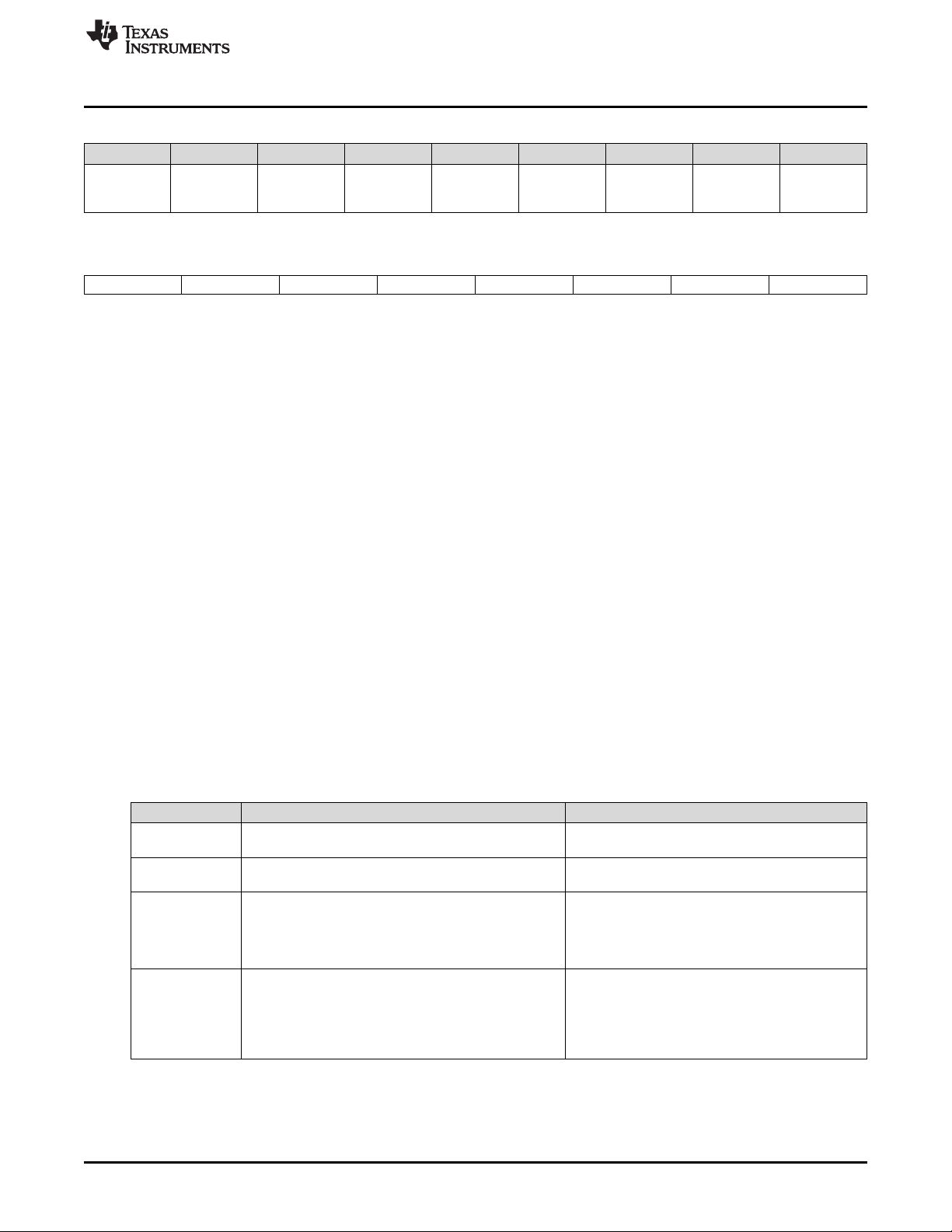
2.4.2 Temperature Enable
This register enables/disables the available temperature sensor options.
www.ti.com
Class Subclass Name Format
Settings Configuration
Bit 7 Bit 6 Bit 5 Bit 4 Bit 3 Bit 2 Bit 1 Bit 0
Low Byte RSVD RSVD RSVD RSVD SOURCE TS3 TS2 TS1
Temperature
Enable
hex 1 0x00 0xFF 0x09 —
Size in
Bytes
Min Max Default Unit
RSVD (Bits 7–4): Reserved
SOURCE (Bit 3): Configure the use of Internal or External temperature sensors for all AFE ports
0 = Use internal temperature sensor(s)
1 = Use external temperature sensor(s)
TS3 (Bit 2): Enable/disable companion AFE temperature sensor TS3, if available
0 = Disable TS3 temperature sensor
1 = Enable TS3 temperature sensor
TS2 (Bit 1): Enable/disable companion AFE temperature sensor TS2, if available
0 = Disable TS2 temperature sensor
1 = Enable TS2 temperature sensor
TS1 (Bit 0): Enable/disable companion AFE temperature sensor TS1
0 = Disable TS1 temperature sensor
1 = Enable TS1 temperature sensor
2.4.3 Temperature Mode Configuration
Each available external temperature sensor can be configured to be used for the cell temperature or FET
temperature features.
12
Basic Measurement System
Copyright © 2015–2018, Texas Instruments Incorporated
SLUUBD3D–September 2015–Revised September 2018
Submit Documentation Feedback
Page 13
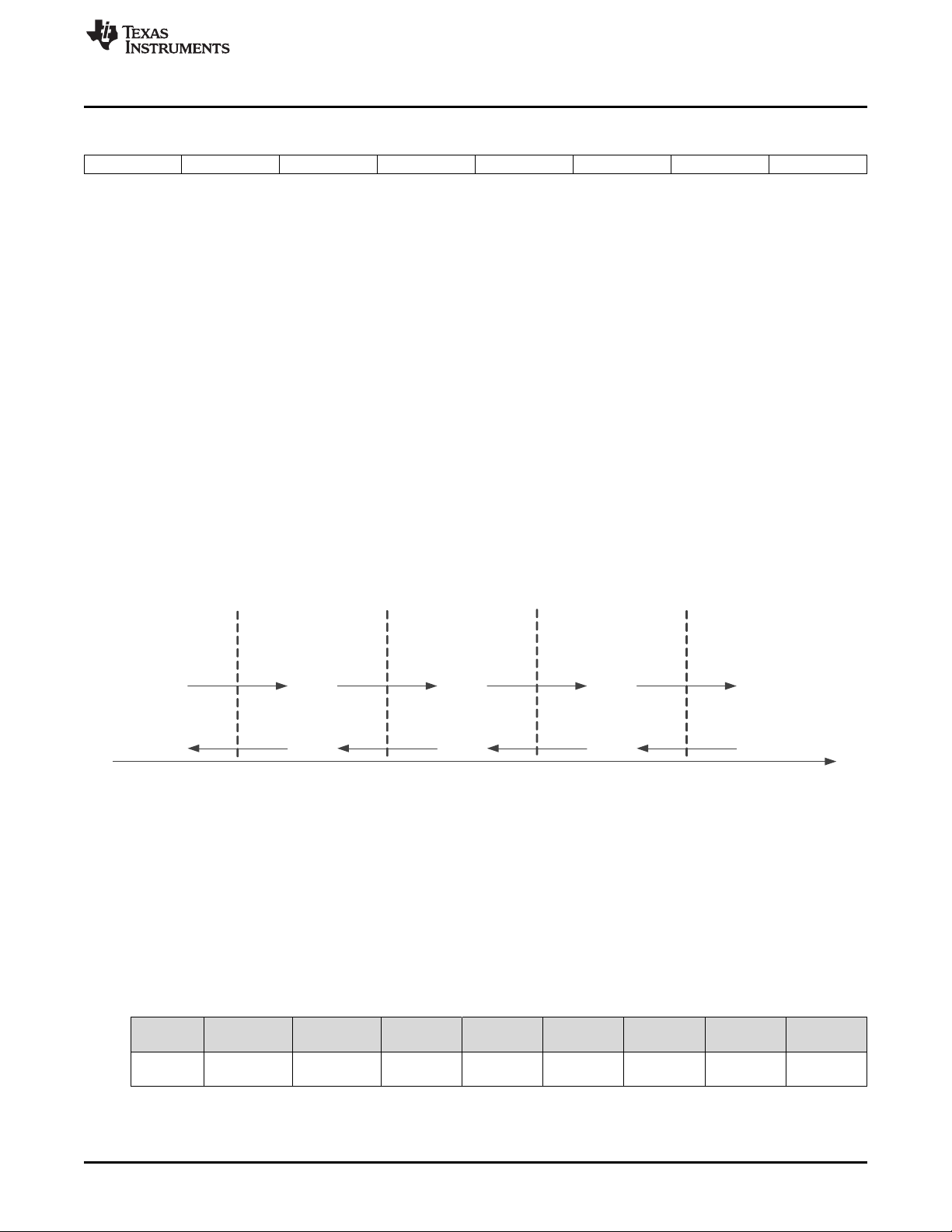
T1
Temperature()
Under Temp
TempRange() [UT]=1
Low Temp
TempRange() [LT]=1
Standard Temp
TempRange() [ST]=1
High Temp
TempRange() [HT]=1
Over Temp
TempRange() [OT]=1
T2
T3 T4
Temperature() > Charge
Inhibit / Suspend Low Temp
+ Hysteresis Temp
Temperature() < Charge
Inhibit / Suspend Low Temp
Temperature() > Pre Charge
Temp + Hysteresis Temp
Temperature() < Pre Charge
Temp
Temperature() > Charge
Inhibit High Temp+
Hysteresis Temp
Temperature() > Charge
Suspend High Temp+
Hysteresis Temp
Temperature() < Charge
Inhibit High Temp
Temperature() < Charge
Suspend High Temp
www.ti.com
Temperature Ranges
Figure 2-1. Temperature Mode
7 6 5 4 3 2 1 0
RSVD RSVD RSVD RSVD RSVD TSMode3 TSMode2 TSMode1
RSVD (Bits 7–3): Reserved
TSMode3 (Bit 2): Select TS3 sensor for Cell or FET Temperature Protection
0 = Use for Cell (default)
1 = Use for FETTemperature()
TSMode2 (Bit 1): Select TS2 sensor for Cell or FET Temperature Protection
0 = Use for Cell (default)
1 = Use for FETTemperature()
TSMode1 (Bit 0): Select TS1 sensor for Cell or FET Temperature Protection
0 = Use for Cell (default)
1 = Use for FETTemperature()
2.5 Temperature Ranges
The measured temperature is segmented into several temperature ranges. The bq78350-R1 uses these
as indication, and, for Lifetime Data Logging, the time spent in each range. The temperature ranges set in
data flash should adhere to the following format:
T1 ≤ T2 ≤ T3 ≤ T4
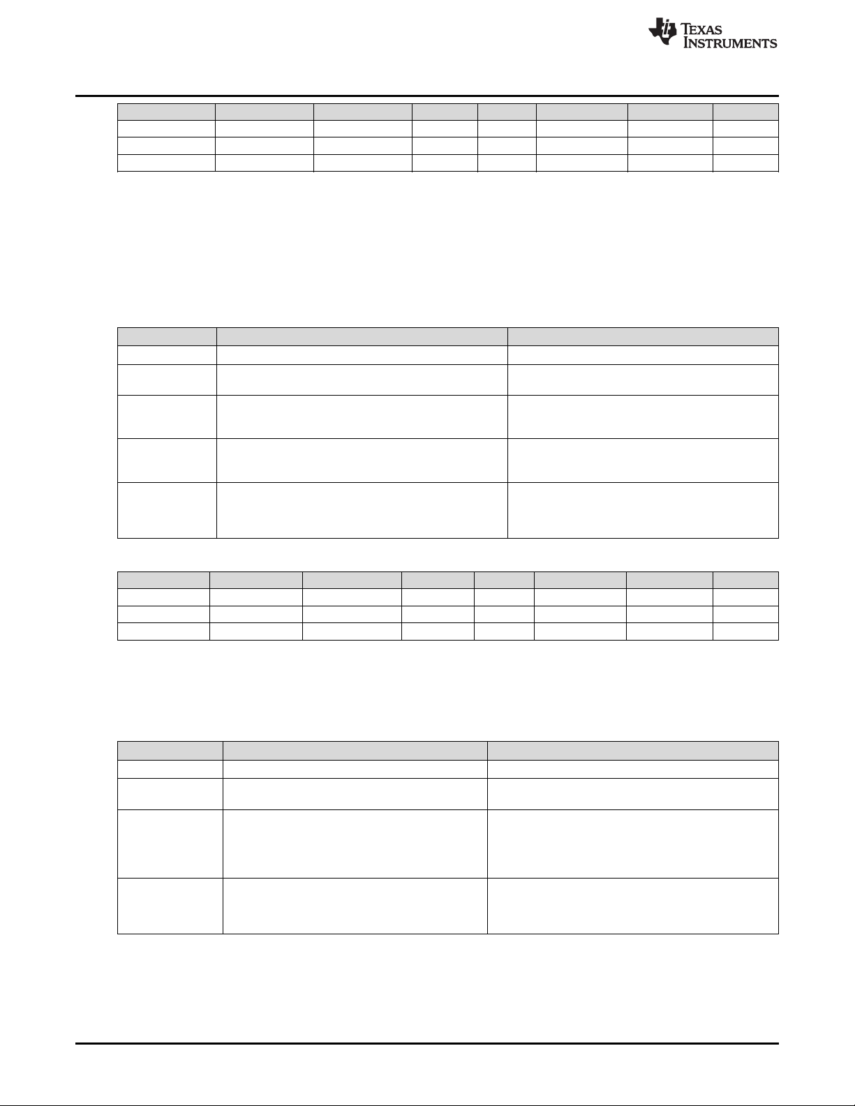
2.6 Basic Configuration Options
2.6.1 DA Configuration
SLUUBD3D–September 2015–Revised September 2018
Submit Documentation Feedback
Figure 2-2. Data Flash Temperature Range Format
See the Temperature Ranges data flash subclass for details on the specific data flash variables.
There are a variety of options available in the bq78350-R1 and the companion AFE that influence the
startup conditions, system configuration, and the data measurement system.
This register is used to configure the setup of various measurement features of the bq78350-R1.
Class Subclass Name Format
Settings Configuration
Configuration
DA
Copyright © 2015–2018, Texas Instruments Incorporated
hex 1 0x00 0xFF 0x11 —
Size in
Bytes
Min Max Default Unit
Basic Measurement System
13
Page 14
Basic Configuration Options
Bit 7 Bit 6 Bit 5 Bit 4 Bit 3 Bit 2 Bit 1 Bit 0
Low Byte FTEMP CTEMP RSVD ExtAveEN VAUXEN VAUX_SCALE
FTEMP (Bit 7): FET Temperature Protection Source
0 = Maximum of external available sources (default)
1 = Average of external available sources
CTEMP (Bit 6): Cell Temperature Protection Source
0 = Maximum of external available sources (default)
1 = Average of external available sources
RSVD (Bit 5): Reserved
ExtAveEN (Bit 4): Enables the bq78350-R1 to measure the BAT input
0 = BAT input is not measured.
1 = BAT input is measured and made available via ExtAveCellVoltage() (default).
VAUXEN (Bit 3): Enables the bq78350-R1 to measure the VAUX input
0 = VAUX input is not measured (default).
1 = VAUX input is measured and made available via VAUXVoltage().
VAUX_SCALE (Bit 2): Enables the bq78350-R1 to scale the VAUXVoltage() data by 10. For example:
Units are 10 mV rather than 1 mV.
0 = VAUXVoltage() is not scaled (resolution is 1 mV) (default).
1 = VAUXVoltage() is scaled (resolution is 10 mV).
IN_SYSTEM_SLEEP (Bit 1): IN SYSTEM SLEEP mode
1 = Enable
0 = Disable (default)
SLEEP (Bit 0): Enables the bq78350-R1 to enter SLEEP mode.
0 = The bq78350-R1 never enters SLEEP mode.
1 = The bq78350-R1 enters SLEEP mode under normal sleep entry criteria (default).
IN_SYSTEM_
SLEEP
www.ti.com
SLEEP
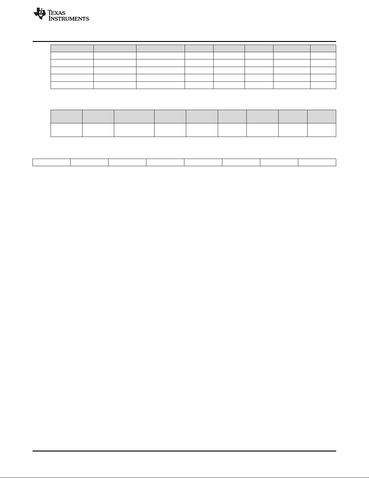
2.6.2 FET Options
This register configures the various FET control options.
Class Subclass Name Format
Settings Configuration FET Options hex 2 0x0000 0xFFFF 0x0021 —
High Byte RSVD RSVD RSVD RSVD RSVD RSVD KEY_POL PCHG_POL
Low Byte RSVD SLEEPCHG CHGFET CHGIN CHGSU OTFET KEY_EN PCHG_EN
RSVD (Bits 7–2): Reserved
KEY_POL: This bit configures the KEYIN input detection polarity.
0 = KEYIN detection is active low (default).
1 = KEYIN detection is active high.
PCHG_POL: Configures the bq78350-R1 PRECHG pin output polarity. If PCHG_EN = 0, then this bit
has no influence.
14
Basic Measurement System
Size in
Bytes
Bit 7 Bit 6 Bit 5 Bit 4 Bit 3 Bit 2 Bit 1 Bit 0
Copyright © 2015–2018, Texas Instruments Incorporated
Min Max Default Unit
SLUUBD3D–September 2015–Revised September 2018
Submit Documentation Feedback
Page 15
www.ti.com
Basic Configuration Options
0 = The bq78350-R1 configures the PRECHG as active low (default).
1 = The bq78350-R1 configures the PRECHG as active high, requiring an external pullup.
SLEEPCHG: CHG FET is enabled during SLEEP.
0 = CHG FET off during SLEEP (default).
1 = CHG FET remains on during SLEEP.
CHGFET: FET action on valid charge termination
0 = FET active
1 = Charging and Precharging disabled, FET off (default)
CHGIN: FET action in CHARGE INHIBIT mode
0 = FET active (default)
1 = Charging and Precharging disabled, FETs off
CHGSU: FET action in CHARGE SUSPEND mode
0 = FET active (default)
1 = Charging and Precharging disabled, FETs off
OTFET: FET action in OVERTEMPERATURE mode
0 = No FET action for overtemperature condition (default)
1 = CHG and DSG FETs will be turned off for overtemperature conditions.
KEY_EN: Enables the bq78350-R1 to use the KEYIN pin function
0 = The bq78350-R1 never uses KEYIN (default).
1 = The bq78350-R1 KEYIN is used to control the DSG FET.
PCHG_EN: Enables the bq78350-R1 to use the PRECHG pin during PRECHARGE mode
0 = The bq78350-R1 never uses PRECHG.
1 = The bq78350-R1 controls PRECHG under normal charge control algorithm (default).
2.6.3 AFE Cell Map
This register maps the cells connected to the companion AFE so that the bq78350-R1 knows cells are
present at the indicated VCx channel.
Class Subclass Name Format
Configuration AFE
High Byte RSVD VC15 VC14 VC13 VC12 VC11 VC10 VC9
Low Byte VC8 VC7 VC6 VC5 VC4 VC3 VC2 VC1
RSVD (Bit 7): Reserved
VCx: Cell connected to this node
1 = A cell is connected to this node and valid measurements are expected.
0 = A cell is NOT connected to this node.
Size in
Bytes
AFE Cell
Map
Bit 7 Bit 6 Bit 5 Bit 4 Bit 3 Bit 2 Bit 1 Bit 0
hex 2 0x0000 0xFFFF 0x0013 —
Min Max Default Unit
SLUUBD3D–September 2015–Revised September 2018
Submit Documentation Feedback
Copyright © 2015–2018, Texas Instruments Incorporated
Basic Measurement System
15
Page 16

Basic Configuration Options
The bq78350-R1 determines which companion AFE is connected by the total number of cells connected.
• When Series Cells = 3 to 5, the bq76920 companion AFE is used.
• When Series Cells = 6 to 10, the bq76930 companion AFE is used.
• When Series Cells = 9 to 15, the bq76940 companion AFE is used.
www.ti.com
16
Basic Measurement System
SLUUBD3D–September 2015–Revised September 2018
Copyright © 2015–2018, Texas Instruments Incorporated
Submit Documentation Feedback
Page 17

3.1 Introduction
The bq78350-R1 supports a wide range of battery and system protection features that are easily
configured or enabled via the integrated data flash. All of the protection items can be enabled or disabled
under Settings:Enable Protections A, Settings:Enable Protections B, and Settings:Enable
Protections C.
If the CHG FET is off and the gauge detects discharge current ≥ Dsg Current Threshold, then the CHG
FET is turned on to protect CHG FET body diode. The CHG FET is turned back off once discharge current
is removed. If the DSG FET is off and the gauge detects charge current ≥ Chg Current Threshold, then
the DSG FET is turned on to protect the DSG FET body diode. The DSG FET is turned back off once
charge current is removed. Body diode protection is always active.
3.1.1 General Protections Configuration
Chapter 3
SLUUBD3D–September 2015–Revised September 2018
Protections
Class Subclass Name Format
Settings Protection
7 6 5 4 3 2 1 0
RSVD RSVD CC_DSG_OFF DC_CHG_OFF LPEN VAUXR
Protection
Configuration
Hex 1 0x00 0xFF 0x00 —
Size in
Bytes
Min Max Default Unit
CUV_RECOV_
CHG
RSVD (Bits 7–6): Reserved
CC_DSG_OFF (Bit 5): Turns DSG FET OFF in current-based charge faults
0 = Disabled (default)
1 = Enabled
DC_CHG_OFF (Bit 4): Turns CHG FET OFF in current-based discharge faults
0 = Disabled (default)
1 = Enabled
LPEN (Bit 3): Protection recovery uses the LOAD_PRESENT flag in the AFE to determine discharge
fault recovery. LOAD_PRESENT should only be used in a low-side protection FET configuration.
0 = Disabled (default)
1 = Enabled
VAUXR (Bit 2): Protection recovery uses the VAUX input as charger present detection.
0 = Disabled (default)
1 = Enabled
CUV_RECOV_CHG (Bit 1): Requires charge to recover SafetyStatus()[CUV]
0 = Disabled (default)
1 = Enabled
RSVD (Bit 0): Reserved
RSVD
SLUUBD3D–September 2015–Revised September 2018
Submit Documentation Feedback
Copyright © 2015–2018, Texas Instruments Incorporated
Protections
17
Page 18

Introduction
3.1.2 Enabled Protections
www.ti.com
Class Subclass Name Format
Settings Protection
7 6 5 4 3 2 1 0
ASCDL ASCD AOLDL AOLD OCD OCC COV CUV
Enabled
Protections
A
Hex 1 0x00 0xFF 0xFF —
Size in
Bytes
Min Max Default Unit
ASCDL (Bit 7): Short Circuit in Discharge Latch
0 = Disabled
1 = Enabled
ASCD (Bit 6): Short Circuit in Discharge recovery. Detection of an ASCD fault cannot be disabled.
0 = Bypassed, auto recovers within 250 ms
1 = Enabled
AOLDL (Bit 5): Overload in Discharge Latch
0 = Disabled
1 = Enabled
AOLD (Bit 4): Overload in Discharge recovery. Detection of an AOLD fault cannot be disabled.
0 = Bypassed, auto recovers within 250 ms
1 = Enabled
OCD (Bit 3): Overcurrent in Discharge
0 = Disabled
1 = Enabled
OCC (Bit 2): Overcurrent in Charge
0 = Disabled
1 = Enabled
COV (Bit 1): Cell Overvoltage
0 = Disabled
1 = Enabled
CUV (Bit 0): Cell Undervoltage
0 = Disabled
1 = Enabled
18
Class Subclass Name Format
Settings Protection
Protections
Enabled
Protections
B
Copyright © 2015–2018, Texas Instruments Incorporated
Size in
Bytes
Hex 1 0x00 0xFF 0x0F —
Min Max Default Unit
SLUUBD3D–September 2015–Revised September 2018
Submit Documentation Feedback
Page 19

www.ti.com
7 6 5 4 3 2 1 0
RSVD OCDL OTF AFE_OVRD UTD UTC OTD OTC
RSVD (Bit 7): Reserved
OCDL (Bit 6): Overcurrent in Discharge Latch
0 = Disabled (default)
1 = Enabled
OTF (Bit 5): Overtemperature Fault
0 = Disabled (default)
1 = Enabled
AFE_OVRD (Bit 4): AFE ALERT
0 = Disabled (default)
1 = Enabled
UTD (Bit 3): Undertemperature in Discharge
0 = Disabled
1 = Enabled
UTC (Bit 2): Undertemperature in Charge
0 = Disabled
1 = Enabled
OTD (Bit 1): Overtemperature in Discharge
0 = Disabled
1 = Enabled
OTC (Bit 0): Overtemperature in Charge
0 = Disabled
1 = Enabled
Introduction
Class Subclass Name Format
Settings Protection
7 6 5 4 3 2 1 0
RSVD RSVD RSVD OC CTOS CTO PTOS PTO
Enabled
Protections
C
Hex 1 0x00 0xFF 0x15 —
Size in
Bytes
Min Max Default Unit
RSVD (Bits 7–5): Reserved. Do not use.
OC (Bit 4): Overcharge
0 = Disabled
1 = Enabled
CTOS (Bit 3): Charging Timeout Suspended
0 = Disabled
1 = Enabled
CTO (Bit 2): Charging Timeout
0 = Disabled
SLUUBD3D–September 2015–Revised September 2018
Submit Documentation Feedback
Copyright © 2015–2018, Texas Instruments Incorporated
Protections
19
Page 20
Introduction
1 = Enabled
PTOS (Bit 1): Precharging Timeout Suspend
0 = Disabled
1 = Enabled
PTO (Bit 0): Precharging Timeout
0 = Disabled
1 = Enabled
3.1.3 Enabled Removal Recovery
The bq78350-R1 offers the option to recover current-based protection by detecting the PRES pin transition
from high to low; for example, the pack is removed and re-inserted into the system.
To enable the replacement recovery, the appropriate bit in Enable Removable Recovery A and Enable
Removable Recovery B should be set. When the bit is set, then the high to low transition of PRES
becomes the only recovery method.
www.ti.com
Table 3-1. Enabled Removal Recovery A
Class Subclass Name Format
Settings Protection
7 6 5 4 3 2 1 0
ASCDL ASCD AOLDL AOLD OCD OCC RSVD RSVD
Enable
Removable
Recovery A
Hex 1 0x00 0xff 0x00 —
Size in
Bytes
Min Max Default Unit
ASCDL (Bit 7): ASCDL Protection Removal recovery
0 = Standard recovery only enabled (default)
1 = Removal recovery only enabled
ASCD (Bit 6): ASCD Protection Removal recovery
0 = Standard recovery only enabled (default)
1 = Removal recovery only enabled
AOLDL (Bit 5): AOLDL Protection Removal recovery
0 = Standard recovery only enabled (default)
1 = Removal recovery only enabled
AOLD (Bit 4): AOLD Protection Removal recovery
0 = Standard recovery only enabled (default)
1 = Removal recovery only enabled
OCD (Bit 3): Precharging Timeout
0 = Standard recovery only enabled (default)
1 = Removal recovery only enabled
OCC (Bit 2): OCC Protection Removal recovery
0 = Standard recovery only enabled (default)
1 = Removal recovery only enabled
RSVD (Bits 1–0): Reserved. Do not use.
20
Protections
SLUUBD3D–September 2015–Revised September 2018
Submit Documentation Feedback
Copyright © 2015–2018, Texas Instruments Incorporated
Page 21
www.ti.com
Table 3-2. Enabled Removal Recovery B
Class Subclass Name Format Size in Bytes Min Max Default Unit
Settings Protection
7 6 5 4 3 2 1 0
RSVD OCDL RSVD RSVD RSVD RSVD RSVD RSVD
Enable
Removable
Recovery B
Hex 1 0x00 0xff 0x00 —
RSVD (Bit 7): Reserved. Do not use.
OCDL (Bit 6): OCDL Protection Removal recovery
0 = Standard recovery only enabled (default)
1 = Removal recovery only enabled
RSVD (Bits 5–0): Reserved. Do not use.
3.1.4 FET Action Options for Current Protections
The bq78350-R1 offers the option to turn off the CHG FET during an overcurrent in discharge (OCD),
overcurrent in discharge latch (OCDL), overload (AOLD), overload latch (AOLDL) or short circuit in
discharge (ASCD), short circuit in discharge latch (ASCDL) faults, or the DSG FET in overcurrent in
charge (OCC) faults.
The CHG FET will turn off for the OCD, OCDL, AOLD, AOLDL, ASCD, and ASCDL faults when
[DC_CHG_OFF] in Protection Configuration is set.
The DSG FET will turn off for the OCC faults when [CC_DSG_OFF] in Protection Configuration is set.
Introduction
3.2 Cell Undervoltage Protection
The device can detect undervoltage in batteries and protect cells from damage by preventing further
discharge.
Upon CUV detection, a snapshot of the measured cell voltages are made available in CUVSnapshot().
This snapshot is available until the next instance of a CUV fault, as this causes the data to be updated to
the latest set of measurements.
Status Condition Action
Normal All Cell voltages in CellVoltage1..15() > CUV:Threshold
Alert
Trip
Recovery
Any Cell voltages in CellVoltage1..15() ≤
CUV:Threshold
Any Cell voltages in CellVoltage1..15() ≤
CUV:Threshold for CUV:Delay duration
SafetyStatus()[CUV] = 1 AND
All Cell voltages in CellVoltage1..15() ≥ CUV:Recovery
AND
Protection Configuration[CUV_RECOV_CHG] = 0 OR
[CUV_RECOV_CHG] = 1
AND Charging detected (that is, BatteryStatus[DSG] = 0)
SafetyAlert()[CUV] = 0
BatteryStatus()[TDA] = 0
SafetyAlert()[CUV] = 1
BatteryStatus()[TDA] = 1
SafetyAlert()[CUV] = 0
SafetyStatus()[CUV] = 1
BatteryStatus()[FD] = 1
OperationStatus()[XDSG] = 1
Discharging is not allowed.
SafetyStatus()[CUV] = 0
BatteryStatus()[FD] = 0, [TDA] = 0
OperationStatus()[XDSG] = 0
Discharging is allowed.
SLUUBD3D–September 2015–Revised September 2018
Submit Documentation Feedback
Copyright © 2015–2018, Texas Instruments Incorporated
Protections
21
Page 22
Cell Overvoltage Protection
Class Subclass Name Type Min Max Default Unit
Protections CUV Threshold I2 0 5000 2500 mV
Protections CUV Delay U1 0 255 2 s
Protections CUV Recovery I2 0 5000 3000 mV
3.3 Cell Overvoltage Protection
The device can detect cell overvoltage in batteries and protect cells from damage by preventing further
charging.
Upon COV detection, a snapshot of the measured cell voltages are made available in COVSnapshot().
This snapshot is available until the next instance of a COV fault, as this causes the data to be updated to
the latest set of measurements.
Status Condition Action
Normal All voltages in CellVoltage1..15() < COV:Threshold SafetyAlert()[COV] = 0
Alert Any voltage in CellVoltage1..15() ≥ COV:Threshold
Trip
Recovery
Recovery
Any voltage in CellVoltage1..15() ≥ COV:Threshold
continuous ≥ COV:Threshold for COV:Delay duration
SafetyStatus()[COV] = 1 AND Protection
Configuration:VAUXR = 0
all voltages in CellVoltage1..15() ≤ COV:Recovery
SafetyStatus()[COV] = 1 AND Protection
Configuration:VAUXR = 1
all voltages in CellVoltage1..15() ≤ COV:Recovery AND
VAUXVoltage() < Power:Charger Present Threshold
www.ti.com
SafetyAlert()[COV] = 1
BatteryStatus()[TCA] = 1
SafetyAlert()[COV] = 0
SafetyStatus()[COV] = 1
BatteryStatus()[TCA] = 0
SafetyStatus()[COV] = 0
BatteryStatus()[TCA] = 0
SafetyStatus()[COV] = 0
BatteryStatus()[TCA] = 0
Class Subclass Name Type Min Max Default Unit
Protections COV Threshold I2 0 32767 4300 mV
Protections COV Delay U1 0 255 2 s
Protections COV Recovery I2 0 32767 4100 mV
3.4 Overcurrent in Charge Protection
The device has overcurrent in charge protection that can be configured to specific current and delay
thresholds to accommodate charging behaviors. See Section 3.1.4 for additional FET action options.
Status Condition Action
Normal Current() < OCC:Threshold SafetyAlert()[OCC] = 0
Alert Current() ≥ OCC:Threshold
Trip
Recovery
Current() continuous ≥ OCC:Threshold for
OCC:Delay duration
[SafetyStatus()[OCC] = 1 AND
Current() continuous ≤ OCC:Recovery Threshold
for OCC:Recovery Delay time
SafetyAlert()[OCC] = 1
BatteryStatus()[TCA] = 1
SafetyAlert()[OCC] = 0
SafetyStatus()[OCC] = 1
BatteryStatus()[TCA] = 0
OperationStatus()[XCHG] = 1
Charging is not allowed.
SafetyStatus()[OCC] = 0
BatteryStatus()[TCA] = 0
OperationStatus()[XCHG] = 0
Charging is allowed.
22
Protections
SLUUBD3D–September 2015–Revised September 2018
Copyright © 2015–2018, Texas Instruments Incorporated
Submit Documentation Feedback
Page 23

www.ti.com
Class Subclass Name Type Min Max Default Unit Description
Protections OCC Threshold I2 –32768 32767 6000 mA
Protections OCC Delay U1 0 255 6 s
Protections OCC
Protections OCC
Recovery
Threshold
Recovery
Delay
I2 –32768 32767 –200 mA
U1 0 255 5 s
3.5 Overcurrent in Discharge Protection
The device has two independent overcurrent in discharge protections that can be set to different current
and delay thresholds to accommodate different load behaviors. See Section 3.1.4 for additional FET
action options.
Status Condition Action
Normal Current() > OCD:Threshold SafetyAlert()[OCDL] = 0, if OCDL counter = 0
Alert OCDL counter > 0
Trip
Latch OCDL counter ≥ OCD:Latch Limit
Recovery
Recovery
Latch Reset SafetyStatus()[OCDL] = 1 for OCD: Reset Time
Current() continuous ≤ OCD:Threshold for
OCD:Delay duration
[SafetyStatus()[OCD] = 1 AND Protection
Configuration:VAUXR = 0
Current() continuous ≥ OCD:Recovery Threshold
for OCD:Recovery Delay time
[SafetyStatus()[OCD] = 1 AND Protection
Configuration:VAUXR = 1
Current() continuous ≥ OCD:Recovery Threshold
for OCD:Recovery Delay time OR VAUXVoltage()
≥ Power:Charger Present Threshold
Overcurrent in Discharge Protection
Overcurrent in Charge trip
threshold
Overcurrent in Charge trip
delay
Overcurrent in Charge
recovery threshold
Overcurrent in Charge
recovery delay
SafetyAlert()[OCDL] = 1, Decrement OCDL counter by
one after each OCD:Counter Dec Delay period
SafetyAlert()[OCD] = 0
SafetyStatus()[OCD] = 1
OperationStatus()[XDSG] = 1
DSG FET is disabled.
Increment OCDL counter.
SafetyAlert()[OCDL] = 0
SafetyStatus()[OCDL] = 1
OperationStatus()[XDSG] = 1
DSG FET is disabled.
SafetyStatus()[OCD] = 0
OperationStatus()[XDSG] = 0
Discharging is allowed.
SafetyStatus()[OCD] = 0
OperationStatus()[XDSG] = 0
Discharging is allowed.
SafetyStatus()[OCDL] = 0
Reset OCDL counter
OperationStatus()[XDSG] = 0
DSG FET returns to normal if SafetyStatus()[OCD] = 0.
Class Subclass Name Type Min Max Default Unit Description
Protections OCD Threshold I2 –32768 32767 –6000 mA Overcurrent in Discharge trip threshold
Protections OCD Delay U1 0 255 6 s Overcurrent in Discharge trip delay
Protections OCD
Protections OCD
Protections OCDL Latch Limit U1 0 255 0 counts Overcurrent in Discharge latch limit
Protections OCDL
Protections OCDL Reset U1 0 255 15 s Overcurrent in Discharge latch reset delay
Recovery
Threshold
Recovery
Delay
Counter Dec
Delay
I2 –32768 32767 200 mA Overcurrent in Discharge recovery threshold
U1 0 255 5 s Overcurrent in Discharge recovery delay
U1 0 255 10 s
SLUUBD3D–September 2015–Revised September 2018
Submit Documentation Feedback
Copyright © 2015–2018, Texas Instruments Incorporated
Overcurrent in Discharge counter decrement
delay
Protections
23
Page 24

Hardware-Based Protection
3.6 Hardware-Based Protection
The bq78350-R1 device has two main hardware-based protections, AOLD and ASCD, with adjustable
current and delay time. Setting ASCD Threshold and Delay [RSNS] doubles the threshold value. It is
located in bit 8 of the ASCD Threshold Delay register. The Threshold settings are in mV; therefore, the
actual current that triggers the protection is based on the R
For details on how to configure the AFE hardware protection, refer to the tables in the companion data
manual, bq769x0 3-Series to 15-Series Cell Battery Monitor Family for Li-Ion and Phosphate Applications
(SLUSBK2).
All of the hardware-based protections provide a short term Trip/Alert/Recovery protection to account for a
current spike as well as a Trip/Alert/Latch protection for persistent faulty condition. The latch feature also
stops the FETs from toggling on and off continuously, preventing damage to the FETs.
In general, when a fault is detected after the Delay time, the DSG FET will be disabled. However, if
Protection Configuration [LPEN] is set, then both FETs are turned off (Trip stage), and an internal fault
counter will be incremented (Alert stage). As the DSG FET is turned off, the current will drop to 0 mA.
After Recovery time, the CHG and DSG FETs will be turned on again (Recovery stage) unless additional
recovery conditions are enabled.
If the alert is caused by a current spike, the fault count will be decremented after Counter Dec Delay
time. If this is a persistent faulty condition, the device will enter the Trip stage after Delay time, and repeat
the Trip/Alert/Recovery cycle. The internal fault counter is incremented every time the device goes through
the Trip/Alert/Recovery cycle. Once the internal fault counter hits the Latch Limit, the protection enters a
Latch stage and the fault will only be cleared through the Latch Reset condition. If Latch Limit is set to 0, it
will latch after the first detection.
The Trip/Alert/Recovery/Latch stages are documented in each of the following hardware-based protection
sections.
used in the schematic design.
SENSE
www.ti.com
3.6.1 Overload in Discharge Protection
The device has a hardware-based overload in discharge protection with adjustable current and delay. See
Section 3.1.4 for additional FET action options.
Status Condition Action
Normal
Alert AOLDL counter > 0
Trip
Latch AOLDL counter ≥ AOLD:Latch Limit
Recovery
Latch Reset
Current() > (AOLD Threshold and
Delay[3:0]/R
Current() continuous ≤ (AOLD Threshold
and Delay[3:0]/R
and Delay[6:4] duration
SafetyStatus()[AOLD] = 1 for
AOLD:Recovery time OR
If Protection Configuration [LPEN] = 1
AND AFEStatus()[LOAD_PRESENT]= 0
SafetyStatus()[AOLDL] = 1
for AOLD:Reset time
SENSE
)
SENSE
) for AOLD Threshold
SafetyAlert()[AOLDL] = 0, if AOLDL counter = 0
SafetyAlert()[AOLDL] = 1
Decrement AOLDL counter by one after each
AOLD:Counter Dec Delay period
SafetyStatus()[AOLD] = 1
OperationStatus()[XDSG] = 1
DSG FET is disabled.
Increment AOLDL counter
SafetyAlert()[AOLDL] = 0
SafetyStatus()[AOLDL] = 1
OperationStatus()[XDSG] = 1
DSG FET is disabled.
SafetyStatus()[AOLD] = 0
OperationStatus()[XDSG] = 0
DSG FET returns to normal if SafetyStatus[AOLDL] = 0.
SafetyStatus()[AOLDL] = 0
Reset AOLDL counter
OperationStatus()[XDSG] = 0
DSG FET returns to normal if SafetyStatus()[AOLD] = 0.
24
Protections
SLUUBD3D–September 2015–Revised September 2018
Copyright © 2015–2018, Texas Instruments Incorporated
Submit Documentation Feedback
Page 25
www.ti.com
This register is representative of the bq769x0 PROTECT 2 register.
Hardware-Based Protection
Class Subclass Name Type Min Max Default Unit
Protections AOLD Threshold and Delay H1 0x00 0xFF 0x00 —
Protections AOLD Latch Limit U1 0 255 0 counts
Protections AOLD Counter Dec Delay U1 0 255 10 s
Protections AOLD Recovery U1 0 255 5 s
Protections AOLD Reset U1 0 255 15 s
Class Subclass Name Format
Settings AOLD
7 6 5 4 3 2 1 0
RSVD OCD_D2 OCD_D1 OCD_D0 OCD_T3 OCD_T2 OCD_T1 OCD_T0
Threshold and
Delay
Hex 1 0x00 0xFF 0x00 —
Size in
Bytes
Min Max Default Unit
RSVD (Bit 7): Reserved. Do not use.
OCD_D2:0 (Bits 6–4): OCD Thresholds Delay Time
000 = 8 ms
001 = 20 ms
010 = 40 ms
011 = 80 ms
100 = 160 ms
101 = 320 ms
110 = 640 ms
111 = 1280 ms
OCD_T3:0 (Bits 3–0): OCD Thresholds with RSNS = 1
0000 = 17 mv
0001 = 22 mv
0010 = 28 mv
0011 = 33 mv
0100 = 39 mv
0101 = 44 mv
0110 = 50 mv
0111 = 56 mv
1000 = 61 mv
1001 = 67 mv
1010 = 72 mv
1011 = 78 mv
1100 = 83 mv
1101 = 89 mv
1110 = 94 mv
1111 = 100 mv
OCD_T3:0 (Bits 3–0): OCD Thresholds with RSNS = 0
0000 = 8 mv
0001 = 11 mv
SLUUBD3D–September 2015–Revised September 2018
Submit Documentation Feedback
Copyright © 2015–2018, Texas Instruments Incorporated
Protections
25
Page 26

Hardware-Based Protection
0010 = 14 mv
0011 = 17 mv
0100 = 19 mv
0101 = 25 mv
0110 = 28 mv
0111 = 31 mv
1000 = 31 mv
1001 = 33 mv
1010 = 36 mv
1011 = 39 mv
1100 = 42 mv
1101 = 44 mv
1110 = 47 mv
1111 = 50 mv
3.6.2 Short Circuit in Discharge Protection
The device has a hardware-based short circuit in discharge protection with adjustable current and delay.
See Section 3.1.4 for additional FET action options.
Status Condition Action
Normal
Alert ASCDL counter > 0
Trip
Latch ASCD counter ≥ ASCD:Latch Limit
Recovery
Latch Reset
Current() > (ASCD Threshold and
Delay[2:0]/R
Current() continuous ≤ (ASCD Threshold
and Delay[2:0]/R
and Delay[7:4] duration
SafetyStatus()[ASCD] = 1 for
ASCD:Recovery time
OR
If Protection Configuration [LPEN] = 1
AND AFEStatus()[LOAD_PRESENT] = 0
SafetyStatus()[ASCDL] = 1
for ASCD:Reset time
SENSE
)
) for ASCD Threshold
SENSE
www.ti.com
SafetyAlert()[ASCDL] = 0, if ASCDL counter = 0
SafetyAlert()[ASCDL] = 1
Decrement ASCDL counter by one after each
SCD:Counter Dec Delay period
SafetyStatus()[ASCD] = 1
OperationStatus()[XDSG] = 1
DSG FET is disabled.
Increment ASCDL counter
SafetyStatus()[ASCD] = 0
SafetyStatus()[ASCDL] = 1
OperationStatus()[XDSG] = 1
DSG FET is disabled.
SafetyStatus()[ASCD] = 0
OperationStatus()[XDSG] = 0
DSG FET returns to normal if SafetyStatus()[ASCDL] = 0.
SafetyStatus()[ASCDL] = 0
OperationStatus()[XDSG] = 0
DSG FET returns to normal if SafetyStatus()[ASCD] = 0.
26
Class Subclass Name Type Min Max Default Unit
Protections ASCD Threshold and Delay H1 0x00 0xFF 0x00 —
Protections ASCD Latch Limit U1 0 255 0 counts
Protections ASCD Counter Dec Delay U1 0 255 10 s
Protections ASCD Recovery U1 0 255 5 s
Protections ASCD Reset U1 0 255 15 s
This register is representative of the bq769x0 PROTECT 1 register.
Protections
Copyright © 2015–2018, Texas Instruments Incorporated
SLUUBD3D–September 2015–Revised September 2018
Submit Documentation Feedback
Page 27

www.ti.com
Hardware-Based Protection
Class Subclass Name Format
Settings ASCD
7 6 5 4 3 2 1 0
RSNS RSVD RSVD SCD_D1 SCD_D0 SCD_T2 SCD_T1 SCD_T0
LEGEND: RSVD = Reserved Location
Threshold and
Delay
Hex 1 0x00 0xFF 0x00 —
Size in
Bytes
Min Max Default Unit
RSNS (Bit 7): AOLD and ASCD Thresholds Divisor
0 = 0.5 × AFE Protection Thresholds (default)
1 = Normal AFE Protection Thresholds
RSVD (Bits 6–5): Reserved. Do not use.
SCD_D1:0 (Bits 4–3): ASCD Delay Time
00 = 70 µs
01 = 100 µs
10 = 200 µs
11 = 400 µs
SCD_T2:0 (Bits 2–0): ASCD Thresholds with RSNS = 1
000 = 44 mv
001 = 67 mv
010 = 89 mv
011 = 111 mv
100 = 133 mv
101 = 155 mv
110 = 178 mv
111 = 200 mv
SCD_T2:0 (Bits 2–0): ASCD Thresholds with RSNS = 0
000 = 22 mv
001 = 33 mv
010 = 44 mv
011 = 56 mv
100 = 67 mv
101 = 78 mv
110 = 89 mv
111 = 100 mv
3.6.3 AFE ALERT OVRD Protection
The device can detect an external override signal sent to the companion bq769x0 AFE that can cause
permanent failure of the battery. This new option provides a temporary fault detection that acts on the
FETs. The permanent failure option is not affected by this change.
SLUUBD3D–September 2015–Revised September 2018
Submit Documentation Feedback
Copyright © 2015–2018, Texas Instruments Incorporated
Protections
27
Page 28
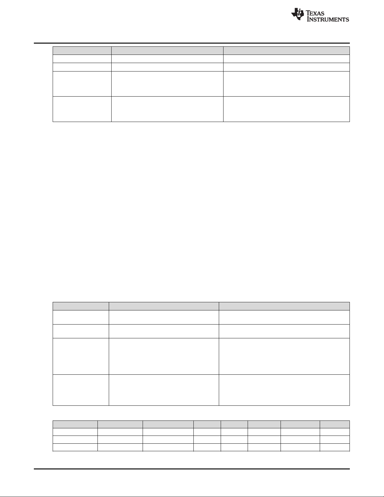
Temperature Protections
Status Condition Action
Normal AFESysStat() [OVRD_ALERT] = 0 SafetyAlert()[AFE_OVRD] = 0
Alert AFESysStat() [OVRD_ALERT] = 1 SafetyAlert()[AFE_OVRD] = 1
Trip
Recovery
AFESysStat() [OVRD_ALERT] = 1 for AFE
External Override Delay duration
AFESysStat() [OVRD_ALERT] = 0 for AFE
External Override Recovery duration
3.7 Temperature Protections
The device provides overtemperature and undertemperature protections based on cell temperature
measurements. The cell temperature based protections are further divided into a protection-in-charging
direction and discharging directions. This section describes in detail each of the protection functions.
For temperature reporting, the device supports a maximum of either three external thermistors or three
internal temperature sensors. The selection of Internal or External temperature sensors is set by
Settings:Temperature Enable[SOURCE]. Unused temperature sensors should be disabled by clearing
the corresponding flag in Settings:Temperature Enable[TS3][TS2][TS1].
The Temperature() command returns the cell temperature measurement. The MAC and extended
command DAStatus2() also returns the temperature measurement from the enabled temperature sensors
and the cell temperature.
The cell temperature based overtemperature and undertemperature safety provide protections in charge
and discharge conditions. The battery pack is considered in CHARGE mode when Battery[DSG] = 0,
where Current() > Chg Current Threshold. The overtemperature and undertemperature in charging
protections are active in this mode. The Battery[DSG] is set to 1 in a NON-CHARGE mode condition,
which includes RELAX and DISCHARGE modes. The overtemperature and undertemperature in
discharge protections are active in these two modes.
www.ti.com
SafetyAlert()[AFE_OVRD] = 0
SafetyStatus()[AFE_OVRD] = 1
OperationStatus()[XCHG, XDSG] = 1
All FETs turn OFF
SafetyAlert()[AFE_OVRD] = 0
SafetyStatus()[AFE_OVRD] = 0
OperationStatus()[XCHG, XDSG] = 0
CHG and DSG FETs allowed to turn ON
3.7.1 Overtemperature in Charge Protection
The device has an overtemperature protection for cells under charge.
Status Condition Action
Normal
Alert
Trip
Recovery
Class Subclass Name Type Min Max Default Unit
Protections OTC Threshold I2 –400 1500 550 0.1°C
Protections OTC Delay U1 0 255 2 s
Protections OTC Recovery I2 –400 1500 500 0.1°C
Cell Temperature in Temperatures() <
OTC:Threshold OR not charging
Cell Temperature in Temperatures() ≥
OTC:Threshold AND charging
Cell Temperature in Temperatures() ≥
OTC:Threshold AND charging for OTC:Delay
duration
SafetyStatus()[OTC] AND Cell Temperature in
Temperatures() ≤ OTC:Recovery
SafetyAlert()[OTC] = 0
SafetyAlert()[OTC] = 1
BatteryStatus()[TCA] = 1
SafetyAlert()[OTC] = 0
SafetyStatus()[OTC] = 1
BatteryStatus()[OTA] = 1
BatteryStatus()[TCA] = 0
OperationStatus()[XCHG] = 1
Charging disabled if FET Options[OTFET] = 1
SafetyStatus()[OTC] = 0
BatteryStatus()[OTA] = 0
BatteryStatus()[TCA] = 0
OperationStatus()[XCHG] = 0
Charging is allowed if FET Options[OTFET] = 1.
28
Protections
SLUUBD3D–September 2015–Revised September 2018
Copyright © 2015–2018, Texas Instruments Incorporated
Submit Documentation Feedback
Page 29
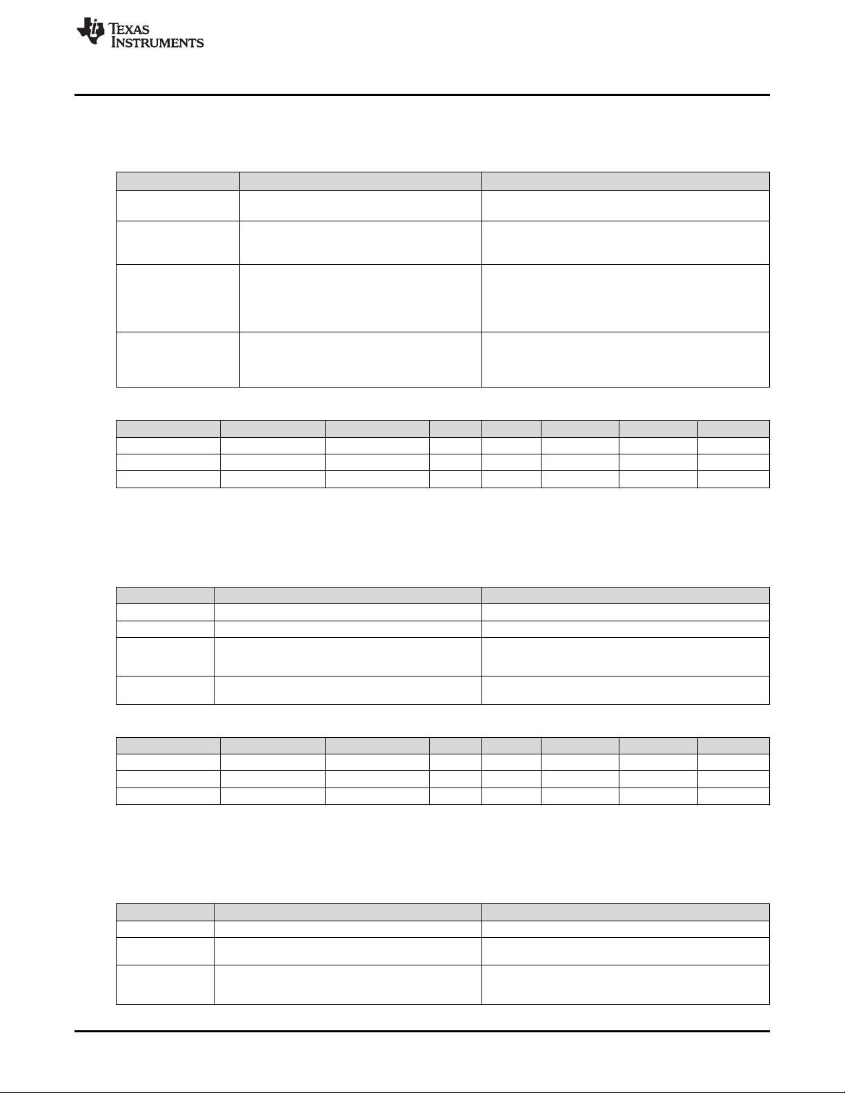
www.ti.com
3.7.2 Overtemperature in Discharge Protection
The device has an overtemperature protection for cells in DISCHARGE state (that is, non-charging state
with BatteryStatus[DSG] = 1).
Status Condition Action
Normal
Alert
Trip
Recovery
Class Subclass Name Type Min Max Default Unit
Protections OTD Threshold I2 –400 1500 600 0.1°C
Protections OTD Delay U1 0 255 2 s
Protections OTD Recovery I2 –400 1500 550 0.1°C
Cell Temperature in Temperatures() <
OTD:Threshold OR charging
Cell Temperature in Temperatures() ≥
OTD:Threshold AND not charging (that is,
BatteryStatus[DSG] = 1)
Cell Temperature in Temperatures() ≥
OTD:Threshold AND not charging (that is,
BatteryStatus[DSG] = 1) for OTD:Delay
duration
SafetyStatus()[OTD] AND Cell Temperature in
Temperatures() ≤ OTD:Recovery
Temperature Protections
SafetyAlert()[OTD] = 0
SafetyAlert()[OTD] = 1
SafetyAlert()[OTD] = 0
SafetyStatus()[OTD] = 1
BatteryStatus()[OTA] = 1
Discharging is disabled AND OperationStatus()[XDSG] =
1 if FET Options[OTFET] = 1.
SafetyStatus()[OTD] = 0
BatteryStatus()[OTA] = 0
Discharging is allowed AND OperationStatus()[XDSG] =
0 if FET Options[OTFET] = 1.
3.7.3 Undertemperature in Charge Protection
The device has an undertemperature protection for cells in charge direction (that is, with
BatteryStatus[DSG] = 0).
Status Condition Action
Normal Temperature() > UTC:Threshold OR not charging SafetyAlert()[UTC] = 0
Alert Temperature() ≤ UTC:Threshold AND charging SafetyAlert()[UTC] = 1
Trip
Recovery
Class Subclass Name Type Min Max Default Unit
Protections UTC Threshold I2 –400 1500 0 0.1°C
Protections UTC Delay U1 0 255 2 s
Protections UTC Recovery I2 –400 1500 50 0.1°C
Temperature() ≤ UTC:Threshold AND
Charging for UTC:Delay duration
SafetyStatus()[UTC] AND
Temperature() ≥ UTC:Recovery
3.7.4 Undertemperature in Discharge Protection
The device has an undertemperature protection for cells in DISCHARGE state (that is, non-charging state
with BatteryStatus[DSG] = 1).
Status Condition Action
Normal Temperature() > UTD:Threshold OR charging SafetyAlert()[UTD] = 0
Alert
Trip
Temperature() ≤ UTD:Threshold AND
Not charging (that is, BatteryStatus[DSG] = 1)
Temperature() ≤ UTD:Threshold AND
Not charging (that is, BatteryStatus[DSG] = 1) for
UTD:Delay duration
SafetyAlert()[UTC] = 0
SafetyStatus()[UTC] = 1
OperationStatus()[XCHG] = 1
SafetyStatus()[UTC] = 0
OperationStatus()[XCHG] = 0
SafetyAlert()[UTD] = 1
SafetyAlert()[UTD] = 0
SafetyStatus()[UTD] = 1
OperationStatus()[XDSG] = 1
SLUUBD3D–September 2015–Revised September 2018
Submit Documentation Feedback
Copyright © 2015–2018, Texas Instruments Incorporated
Protections
29
Page 30

Temperature Protections
Status Condition Action
Recovery
Class Subclass Name Type Min Max Default Unit
Protections UTD Threshold I2 –400 1500 0 0.1°C
Protections UTD Delay U1 0 255 2 s
Protections UTD Recovery I2 –400 1500 50 0.1°C
SafetyStatus()[UTD] AND
Temperature() ≥ UTD:Recovery
3.7.5 Overtemperature FET Protection
The device has an overtemperature protection to limit the FET temperature.
NOTE: This feature is only available when using the bq76930x or bq76940x device: There is only
one external TS available in the bq76920 and this is used for cell temperature.
Status Condition Action
Normal FETTemperature() < OTF:Threshold SafetyAlert()[OTF] = 0
Alert FETTemperature() ≥ OTF:Threshold
Trip
Recovery
FETTemperature() ≥ OTF:Threshold for
OTF:Delay duration
SafetyStatus()[OTF] AND FETTemperature() ≤
OTF:Recovery
www.ti.com
SafetyStatus()[UTD] = 0
OperationStatus()[XDSG] = 0
SafetyAlert()[OTF] = 1
BatteryStatus()[TDA] = 1, [TCA] = 1
SafetyAlert()[OTF] = 0
SafetyStatus()[OTF] = 1
BatteryStatus()[OTA] = 1
BatteryStatus()[TDA] = 0, [TCA] = 0
OperationStatus()[XCHG][XDSG] = 1,1 if FET
Options[OTFET] = 1
SafetyStatus()[OTF] = 0
BatteryStatus()[OTA] = 0
BatteryStatus()[TDA] = 0, [TCA] = 0
OperationStatus()[XCHG][XDSG] = 0,0
3.8 Precharge Timeout Protection
The device can measure the precharge time and stop charging if it exceeds the adjustable period.
Status Condition Action
Enable
Suspend or Recovery Current() < PTO:Suspend Threshold
Trip PTO timer > PTO:Delay
Reset
Class Subclass Name Type Min Max Default Unit
Protections PTO Charge Threshold I2 –32768 32767 2000 mA
Protections PTO Suspend Threshold I2 –32768 32767 1800 mA
Protections PTO Delay U2 0 65535 1800 s
Protections PTO Reset I2 –32768 32767 2 mAh
Current() > PTO:Charge Threshold AND
ChargingStatus()[PCHG] = 1
SafetyStatus()[PTO] = 1 AND
(Discharge by an amount of PTO:Reset)
Start PTO timer
SafetyAlert()[PTOS] = 0
Stop PTO timer
SafetyAlert()[PTOS] = 1
Stop PTO timer
SafetyStatus()[PTO] = 1
BatteryStatus()[TCA] = 1
Charging is not allowed.
Stop and reset PTO timer
SafetyAlert()[PTOS] = 0
SafetyStatus()[PTO] = 0
BatteryStatus()[TCA] = 0
Charging is allowed.
30
Protections
SLUUBD3D–September 2015–Revised September 2018
Copyright © 2015–2018, Texas Instruments Incorporated
Submit Documentation Feedback
Page 31

www.ti.com
3.9 Fast Charge Timeout Protection
The device can measure the charge time and stop charging if it exceeds the adjustable period.
Status Condition Action
Enable Current() > CTO:Charge Threshold
Suspend or Recovery Current() < CTO:Suspend Threshold
Trip CTO time > CTO:Delay
Reset
Class Subclass Name Type Min Max Default Unit
Protections CTO Charge Threshold I2 –32768 32767 2500 mA
Protections CTO Suspend Threshold I2 –32768 32767 2000 mA
Protections CTO Delay U2 0 65535 54000 s
Protections CTO Reset I2 –32768 32767 2 mAh
SafetyStatus()[CTO] = 1 AND
(Discharge by an amount of CTO:Reset)
Fast Charge Timeout Protection
Start CTO timer
SafetyAlert()[CTOS] = 0
Stop CTO timer
SafetyAlert()[CTOS] = 1
Stop CTO timer
SafetyStatus()[CTO] = 1
BatteryStatus()[TCA] = 1
Charging is not allowed.
Stop and reset CTO timer
SafetyAlert()[CTOS] = 0
SafetyStatus()[CTO] = 0
BatteryStatus()[TCA] = 0
Charging is allowed.
3.10 Overcharge Protection
The device can prevent continuing charging if the pack is charged in excess over FullChargeCapacity().
While RemainingCapacity() never reports a value higher than FullChargeCapacity() in the device registers,
it is tracked to higher values internally to protect against overcharging.
Status Condition Action
Normal RemainingCapacity() < FullChargeCapacity() SafetyAlert()[OC] = 0
Alert RemainingCapacity() ≥ FullChargeCapacity() SafetyAlert()[OC] = 1
Trip
Recovery
Class Subclass Name Type Min Max Default Unit
Protections OC Threshold I2 –32768 32767 300 mAh
Protections OC Recovery I2 –32768 32767 2 mAh
Protections OC RSOC Recovery U1 0% 100% 90%
RemainingCapacity() ≥ FullChargeCapacity() +
OC:Threshold
SafetyStatus()[OC] = 1 AND
continuous discharge of Recovery OR
RemainingStateOfCharge() < OC:RSOC
Recovery
SafetyAlert()[OC] = 0
SafetyStatus()[OC] = 1
BatteryStatus()[TCA] = 1, [OCA] = 1 if the device is in
CHARGE state (that is, BatteryStatus[DSG] = 0).
OperationStatus()[XCHG] = 1
Charging is not allowed.
SafetyStatus()[OC] = 0
BatteryStatus()[TCA] = 0, [OCA] = 0
OperationStatus()[XCHG] = 0
Charging is allowed.
SLUUBD3D–September 2015–Revised September 2018
Submit Documentation Feedback
Copyright © 2015–2018, Texas Instruments Incorporated
Protections
31
Page 32

4.1 Introduction
The device can permanently disable the use of the battery pack in case of a severe failure. The
permanent failure checks, except for IFC and DFW, can be individually enabled or disabled by setting the
appropriate bit in Settings:Enabled PF A, Settings:Enabled PF B, Settings:Enabled PF C, and
Settings:Enabled PF D. All permanent failure checks except for IFC and DFW are disabled until
ManufacturingStatus()[PF] is set. When any PFStatus() bit is set, the device enters PERMANENT FAIL
mode and the following actions are taken in sequence:
1. Precharge, charge, and discharge FETs are turned off.
2. OperationStatus()[PF] = 1
3. The following SBS data is changed: BatteryStatus()[TCA] = 1, BatteryStatus()[TDA] = 1,
ChargingCurrent() = 0, and ChargingVoltage() = 0.
4. A backup of the internal AFE hardware registers are written to data flash: AFE Status, AFE Config,
AFE VCx, and AFE Data.
5. The black box data of the last three SafetyStatus() changes leading up to PF with the time difference is
written into the black box data flash along with the 1stPFStatus() value.
6. The following SBS values are preserved in data flash for failure analysis:
• SafetyAlert()
• SafetyStatus()
• PFAlert()
• PFStatus()
• OperationStatus()
• ChargingStatus()
• GaugingStatus()
• Voltages in DAStatus1()
• Current()
• TS1, TS2, and TS3 from DAStatus2()
7. Data flash writing is disabled (except to store subsequent PFStatus() flags).
8. The SAFE pin is driven high if configured for specific failures and Voltage() is above 3500 mV or there
is a CHG FET (CFETF) or DSG FET (DFETF) failure. The SAFE pin will remain asserted until the
Fuse Blow Timeout expired.
While the device is in PERMANENT FAIL mode, any new SafetyAlert(), SafetyStatus(), PFAlert(), and
PFStatus() flags that are set are added to the permanent fail log. Any new PFStatus() flags that occur
during PERMANENT FAIL mode can trigger the SAFE pin. In addition, new PFStatus() flags are recorded
in the Black Box Recorder 2ndand 3rdPF Status entries.
Chapter 4
SLUUBD3D–September 2015–Revised September 2018
Permanent Fail
4.2 Permanent Failure Configuration
The following configuration registers allow the various permanent failure detection features to be enabled
or disabled. If disabled (default), the feature takes no action including setting flags in PFAlert() or
PFStatus().
32
Permanent Fail
Copyright © 2015–2018, Texas Instruments Incorporated
SLUUBD3D–September 2015–Revised September 2018
Submit Documentation Feedback
Page 33

www.ti.com
Permanent Failure Configuration
Class Subclass Name Format
Settings
7 6 5 4 3 2 1 0
DFETF CFETF VIMR SOT SOCD SOCC SOV SUV
Permanent
Failure
Enabled PF
A
Hex 1 0x00 0xFF 0x00 —
Size in
Bytes
Min Max Default Unit
DFETF (Bit 7): Discharge FET
1 = Enabled
0 = Disabled (default)
CFETF (Bit 6): Charge FET
1 = Enabled
0 = Disabled (default)
VIMR (Bit 5): Voltage imbalance at rest
1 = Enabled
0 = Disabled (default)
SOT (Bit 4): Safety Overtemperature Cell
1 = Enabled
0 = Disabled (default)
SOCD (Bit 3): Safety Overcurrent in Discharge
1 = Enabled
0 = Disabled (default)
SOCC (Bit 2): Safety Overcurrent in Charge
1 = Enabled
0 = Disabled (default)
SOV (Bit 1): Safety overvoltage
1 = Enabled
0 = Disabled (default). This feature cannot be stopped from turning the appropriate FETs OFF
as this is a hardware feature of the companion AFE.
SUV (Bit 0): Safety undervoltage
1 = Enabled
0 = Disabled (default). This feature cannot be stopped from turning the appropriate FETs OFF
as this is a hardware feature of the companion AFE.
Class Subclass Name Format
Settings
SLUUBD3D–September 2015–Revised September 2018
Submit Documentation Feedback
Permanent
Failure
Enabled PF
B
Copyright © 2015–2018, Texas Instruments Incorporated
Size in
Bytes
Hex 1 0x00 0xFF 0x00 —
Min Max Default Unit
Permanent Fail
33
Page 34

Enabling Use of the SAFE Pin
7 6 5 4 3 2 1 0
SOTF TS3 TS2 TS1 AFE_XRDY AFE_OVRD AFEC AFER
SOTF (Bit 7): Safety Overtemperature FET
1 = Enabled
0 = Disabled (default)
TS3 (Bit 6): Temperature sensor 3
1 = Enabled
0 = Disabled (default)
TS2 (Bit 5): Temperature sensor 2
1 = Enabled
0 = Disabled (default)
TS1 (Bit 4): Temperature sensor 1
1 = Enabled
0 = Disabled (default)
AFE_XRDY (Bit 3): Companion AFE XREADY
1 = Enabled
0 = Disabled (default)
AFE_OVRD (Bit 2): Companion AFE OVERRIDE
1 = Enabled
0 = Disabled (default)
AFEC (Bit 1): AFE Communication
1 = Enabled
0 = Disabled (default)
AFER (Bit 0): AFE Register
1 = Enabled
0 = Disabled (default)
www.ti.com
4.3 Enabling Use of the SAFE Pin
The AFE pin can be enabled or disabled for use for any of the enabled protections through the settings in
the following:
Class Subclass Name Format
Settings Fuse PF SAFE A Hex 1 0x00 0xFF 0x00 —
7 6 5 4 3 2 1 0
DFETF CFETF VIMR SOT SOCD SOCC SOV SUV
DFETF (Bit 7): Discharge FET
1 = Enabled
0 = Disabled (default)
CFETF (Bit 6): Charge FET
34
Permanent Fail
Copyright © 2015–2018, Texas Instruments Incorporated
Size in
Bytes
Min Max Default Unit
SLUUBD3D–September 2015–Revised September 2018
Submit Documentation Feedback
Page 35

www.ti.com
Enabling Use of the SAFE Pin
1 = Enabled
0 = Disabled (default)
VIMR (Bit 5): Voltage Imbalance at Rest
1 = Enabled
0 = Disabled (default)
SOT (Bit 4): Safety Overtemperature Cell
1 = Enabled
0 = Disabled (default)
SOCD (Bit 3): Safety Overcurrent in Discharge
1 = Enabled
0 = Disabled (default)
SOCC (Bit 2): Safety Overcurrent in Charge
1 = Enabled
0 = Disabled (default)
SOV (Bit 1): Safety Overvoltage
1 = Enabled
0 = Disabled (default)
SUV (Bit 0): Safety Undervoltage
1 = Enabled
0 = Disabled (default)
Class Subclass Name Format
Settings Fuse PF SAFE B Hex 1 0x00 0xFF 0x00 —
7 6 5 4 3 2 1 0
SOTF TS3 TS2 TS1 AFE_XRDY AFE_OVRD AFEC AFER
Size in
Bytes
Min Max Default Unit
SOTF (Bit 7): Safety Overtemperature FET
1 = Enabled
0 = Disabled (default)
TS3 (Bit 6): TS3
1 = Enabled
0 = Disabled (default)
TS2 (Bit 5): TS2
1 = Enabled
0 = Disabled (default)
TS1 (Bit 4): TS1
1 = Enabled
0 = Disabled (default)
AFE_XRDY (Bit 3): AFE XREADY
1 = Enabled
0 = Disabled (default)
SLUUBD3D–September 2015–Revised September 2018
Submit Documentation Feedback
Copyright © 2015–2018, Texas Instruments Incorporated
Permanent Fail
35
Page 36
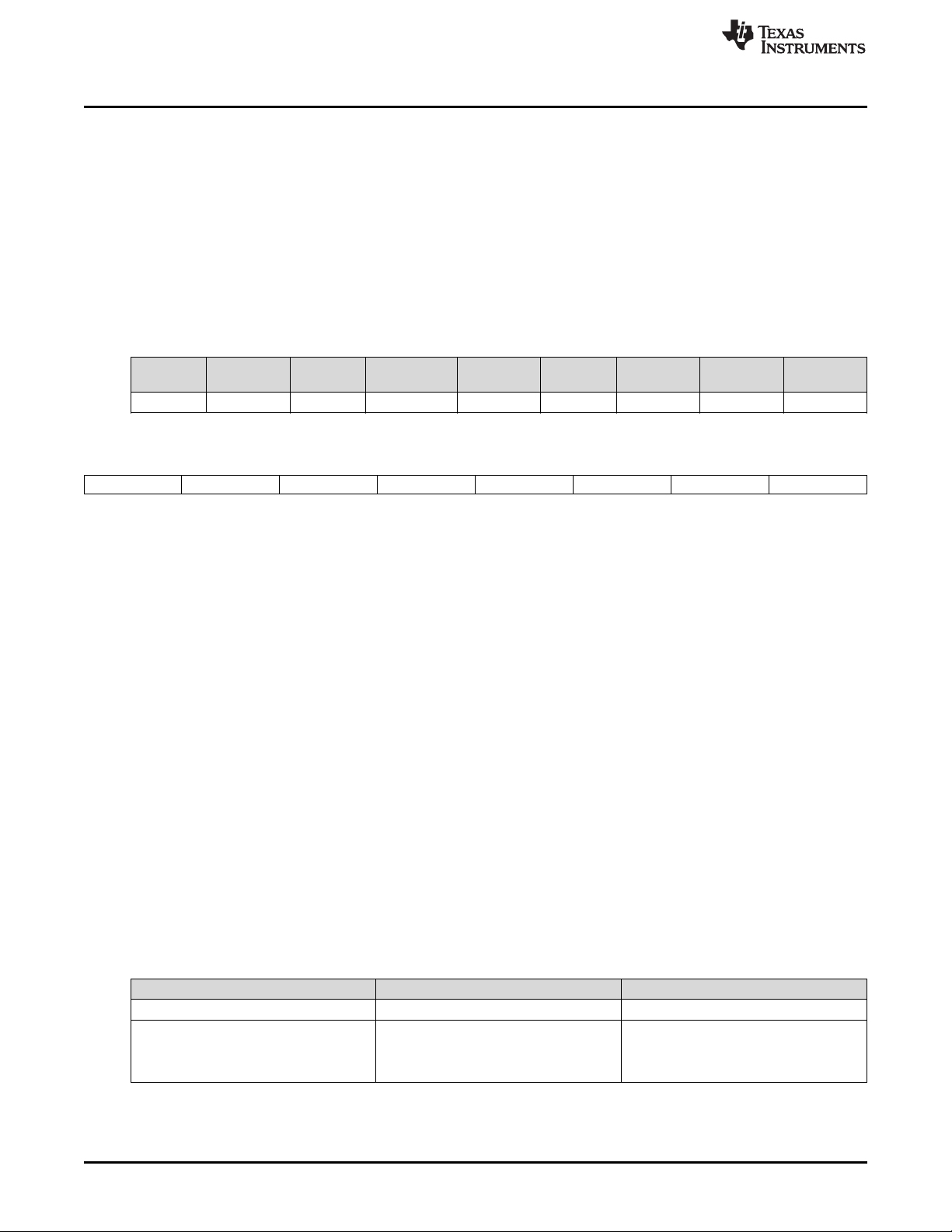
Safety Cell Undervoltage Permanent Fail
AFE_OVRD (Bit 2): AFE Override
1 = Enabled
0 = Disabled (default)
AFEC (Bit 1): AFE Communication
1 = Enabled
0 = Disabled (default)
AFER (Bit 0): AFE Register
1 = Enabled
0 = Disabled (default)
www.ti.com
Class Subclass Name Format
Settings Fuse PF SAFE C Hex 1 0x00 0xFF 0x00 —
7 6 5 4 3 2 1 0
RSVD RSVD RSVD RSVD RSVD RSVD DFW IFC
Size in
Bytes
Min Max Default Unit
RSVD (Bits 7–2): Reserved
DFW (Bit 1): Data flash write
1 = Enabled
0 = Disabled (default)
IFC (Bit 0): Instruction flash checksum
1 = Enabled
0 = Disabled (default)
The bq78350-R1 has a minimum voltage required to attempt to blow a fuse through SAFE activation. This
is a pack-based value of 3500 mV. Voltage scaling (VSCALE) should be enabled if the supported battery
pack voltage is higher than 32767 mV. This value is automatically internally adjusted for any VSCALE
setting. FET failures bypass this requirement to activate SAFE.
4.4 Safety Cell Undervoltage Permanent Fail
The bq78350-R1 uses the UV Protection function of the companion AFE for this feature and can be
configured to permanently disable the battery in the case of severe undervoltage in any of the cells. This
feature cannot be disabled.
The voltage threshold setting is set in AFE SUV:Threshold, which the device will map to the available
settings in the companion AFE with the maximum setting of 3131 mV and the minimum of 1568 mV.
The delay timing configuration for this feature is combined in the same register with the delay time of the
Safety Overvoltage feature.
36
Permanent Fail
Status Condition Action
Normal AFEStatus() [UV] = 0 PFStatus()[SUV] = 0
PFStatus()[SUV] = 1
Trip AFEStatus() [UV] = 1
SLUUBD3D–September 2015–Revised September 2018
Copyright © 2015–2018, Texas Instruments Incorporated
BatteryStatus()[FD] = 1
BatteryStatus()[TDA] = 1
BatteryStatus()[TCA] = 1
Submit Documentation Feedback
Page 37
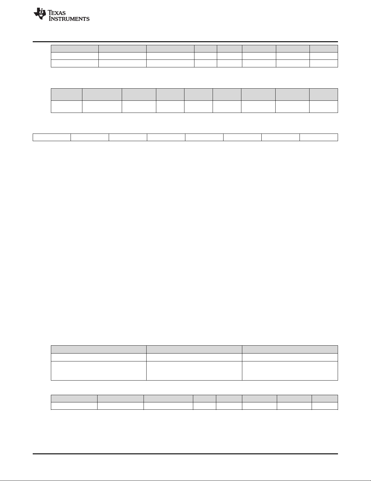
www.ti.com
This register is representative of the bq769x0 PROTECT 3 register.
Safety Cell Overvoltage Permanent Fail
Class Subclass Name Type Min Max Default Unit
Permanent Fail AFE SUV Threshold I2 1580 3100 1750 mV
Permanent Fail AFE SOV/AFE SUV SOV and SUV Delay U1 0 255 2 s
Class Subclass Name Format
Settings
7 6 5 4 3 2 1 0
SUV_D1 SUV_D0 SOV_D1 SOV_D0 RSVD RSVD RSVD RSVD
LEGEND: R/W = Read/Write; R = Read only; -n = value after reset
AFE SOV/AFE
SUV
SOV and SUV
Delay
Hex 1 0x00 0xF0 0x50 —
Size in
Bytes
Min Max Default Unit
SUV_D1:0 (Bits 7–6): Safety Undervoltage Delay Time
00 = 1 s
01 = 4 s
10 = 8 s
11 = 16 s
SOV_D1:0 (Bits 5–4): Safety Overvoltage Delay Time
00 = 1 s
01 = 2 s
10 = 4 s
11 = 8 s
RSVD: (Bits 3–0): Reserved
4.5 Safety Cell Overvoltage Permanent Fail
The bq78350-R1 uses the OV Protection function of the companion AFE for this feature and can be
configured to permanently disable the battery in the case of severe overvoltage in any of the cells. This
feature cannot be disabled.
The voltage threshold setting is set in AFE SOV:Threshold, which the device will map to the available
settings in the companion AFE with the maximum setting of 4703 mV and the minimum of 3140 mV.
The delay timing configuration for this feature is combined in the same register with the delay time of the
Safety Undervoltage feature.
Status Condition Action
Normal AFEStatus() [OV] = 0 PFStatus()[SOV] = 0
Trip AFEStatus() [OV] = 1
Class Subclass Name Type Min Max Default Unit
Permanent Fail AFE SOV Threshold I2 3150 4700 4350 mV
4.6 Safety Overcurrent in Charge Permanent Fail
The device can permanently disable the battery in the case of a severe OVERCURRENT IN CHARGE
state.
PFStatus()[SOV] = 1
BatteryStatus()[TDA] = 1
BatteryStatus()[TCA] = 1
SLUUBD3D–September 2015–Revised September 2018
Submit Documentation Feedback
Copyright © 2015–2018, Texas Instruments Incorporated
Permanent Fail
37
Page 38

Safety Overcurrent in Discharge Permanent Fail
Status Condition Action
Normal Current() < SOCC:Threshold PFAlert()[SOCC] = 0
Alert Current() ≥ SOCC:Threshold
Trip Current() ≥ SOCC:Threshold for SOCC:Delay duration
4.7 Safety Overcurrent in Discharge Permanent Fail
The device can permanently disable the battery in the case of severe overcurrent in DISCHARGE or
RELAX state.
Status Condition Action
Normal Current() > SOCD:Threshold PFAlert()[SOCD] = 0
Alert Current() ≤ SOCD:Threshold
Trip Current() ≤ SOCD:Threshold for SOCD:Delay duration
www.ti.com
PFAlert()[SOCC] = 1
BatteryStatus()[TCA] = 1
BatteryStatus()[OCA] = 1
PFAlert()[SOCC] = 0
PFStatus()[SOCC] = 1
BatteryStatus()[TCA] = 1
BatteryStatus()[TDA] =1
BatteryStatus()[OCA] = 1
PFAlert()[SOCD] = 1
BatteryStatus()[TDA] = 1
PFAlert()[SOCD] = 0
PFStatus()[SOCD] = 1
BatteryStatus()[TCA] = 1
BatteryStatus()[TDA] =1
4.8 Safety Overtemperature Cell Permanent Fail
The device can permanently disable the battery pack in case of severe overtemperature of the cells
detected using the external TS1...3 temperature sensor(s), which are configured to report Temperature().
The Temperature() measurement configuration is controlled by setting the corresponding flag in DA
Configuration.
Status Condition Action
Normal Cell Temperature in DAStatus2() < SOT:Threshold PFAlert()[SOT] = 0
Alert Cell Temperature in DAStatus2() ≥ SOT:Threshold
Trip
Class Subclass Name Type Min Max Default Unit
Permanent Fail SOT Threshold I2 –400 1500 650 0.1°C
Permanent Fail SOT Delay U1 0 255 5 s
Cell Temperature in DAStatus2() continuous ≥
SOT:Threshold for SOT:Delay duration
4.9 Safety Overtemperature FET (SOTF) Permanent Fail
The device can disable the battery pack permanently in case of severe overtemperature on the power
FET. The temperature sensor(s) can be configured to report as FET Temperature in DAStatus2() by
setting the corresponding flags in Temperature Mode and DA Configuration[FTEMP].
PFAlert()[SOT] = 1
BatteryStatus()[OTA] = 1
PFAlert()[SOT] = 0
PFStatus()[SOT] = 1
BatteryStatus()[OTA] = 1
BatteryStatus()[TCA] = 1
BatteryStatus()[TDA] = 1
38
Permanent Fail
Status Condition Action
Normal FET Temperature in DAStatus2() < SOTF:Threshold PFAlert()[SOTF] = 0
Alert FET Temperature in DAStatus2() ≥ SOTF:Threshold
SLUUBD3D–September 2015–Revised September 2018
Copyright © 2015–2018, Texas Instruments Incorporated
PFAlert()[SOTF] = 1
BatteryStatus()[OTA] = 1
Submit Documentation Feedback
Page 39
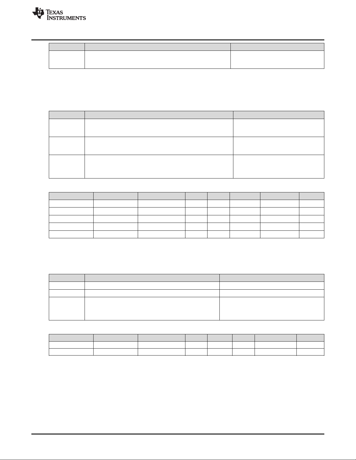
www.ti.com
Status Condition Action
Trip
FET Temperature in DAStatus2() continuous ≥ SOTF:Threshold for
SOTF:Delay duration
4.10 Voltage Imbalance at Rest Permanent Fail
The device can permanently disable the battery pack in case of a voltage difference between the cells in a
stack while at rest.
Status Condition Action
Normal
Alert
Trip
Class Subclass Name Type Min Max Default Unit
Permanent Fail VIMR Check Voltage I2 0 5000 5000 mV
Permanent Fail VIMR Check Current I2 0 32767 10 mA
Permanent Fail VIMR Delta Threshold I2 0 5000 500 mV
Permanent Fail VIMR Delta Delay U1 0 255 5 s
Permanent Fail VIMR Duration U2 0 65535 100 s
CellVoltage1..15() < VIMR:Check Voltage OR
|Current()| > VIMR:Check Current OR
Δ(CellVoltage1..15()) < VIMR:Delta Threshold
Any(CellVoltage1..15()) ≥ VIMR:Check Voltage AND
|Current()| < VIMR:Check Current for VIMR:Duration AND
Δ(CellVoltage1..15()) ≥ VIMR:Delta Threshold
Any(CellVoltage1..15()) ≥ VIMR:Check Voltage AND
|Current()| < VIMR:Check Current for VIMR:Duration AND
Δ(CellVoltage1..15()) ≥ VIMR:Delta Threshold for VIMR:Delta Delay
Voltage Imbalance at Rest Permanent Fail
PFAlert()[SOTF] = 0
PFStatus()[SOTF] = 1
BatteryStatus()[OTA] = 1
PFAlert()[VIMR] = 0
PFAlert()[VIMR] = 1
PFAlert()[VIMR] = 0
PFStatus()[VIMR] = 1
BatteryStatus()[TCA] = 1
BatteryStatus()[TDA] = 1
4.11 Charge FET Permanent Fail
The device can permanently disable the battery pack in case the charge FET is not working properly.
Status Condition Action
Normal CHG FET off AND Current() < CFET:OFF Threshold PFAlert()[CFETF] = 0
Alert CHG FET off AND Current() ≥ CFET:OFF Threshold PFAlert()[CFETF] = 1
Trip
Class Subclass Name Type Min Max Default Unit
Permanent Fail CFETF OFF Threshold I2 0 500 5 mA
Permanent Fail CFETF Delay U1 0 255 5 s
CHG FET off AND Current() continuously ≥ CFET:OFF
Threshold for CFET:OFF Delay duration
4.12 Discharge FET Permanent Fail
The device can permanently disable the battery pack in case the discharge FET is not working properly.
PFAlert()[CFETF] = 0
PFStatus()[CFETF] = 1
BatteryStatus()[TCA] = 1
BatteryStatus()[TDA] = 1
SLUUBD3D–September 2015–Revised September 2018
Submit Documentation Feedback
Copyright © 2015–2018, Texas Instruments Incorporated
Permanent Fail
39
Page 40

External Override Permanent Fail
Status Condition Action
Normal DSG FET off AND Current() > DFET:OFF Threshold PFAlert()[DFETF] = 0
Alert DSG FET off AND Current() ≤ DFET:OFF Threshold PFAlert()[DFETF] = 1
Trip
Class Subclass Name Type Min Max Default Unit
Permanent Fail DFET OFF Threshold I2 –500 0 –5 mA
Permanent Fail DFET Delay U1 0 255 5 s
DSG FET off AND Current() continuously ≤ DFET:OFF
Threshold for DFET:OFF Delay duration
4.13 External Override Permanent Fail
The device can detect an external override signal sent to the companion bq769x0 AFE, which can cause
permanent failure of the battery. This can be used to indicate to the bq78350-R1 that an external circuit,
such as an independent voltage protection circuit, has disabled the battery permanently.
Status Condition Action
Normal AFESysStat() [OVRD_ALERT] = 0 PFAlert()[AFE_OVRD] = 0
Alert AFESysStat() [OVRD_ALERT] = 1 PFAlert()[AFE_OVRD] = 1
Trip
AFESysStat() [OVRD_ALERT] = 1 continuously for AFE
External Override: Delay duration
www.ti.com
PFAlert()[DFETF] = 0
PFStatus()[DFETF] = 1
BatteryStatus()[TCA] = 1
BatteryStatus()[TDA] = 1
PFAlert()[AFE_OVRD] = 0
PFStatus()[AFE_OVRD] = 1
Class Subclass Name Type Min Max Default Unit
Permanent Fail AFE External Override Delay U1 0 255 5 s
4.14 AFE Register Permanent Fail
The device compares the AFE hardware register periodically with a RAM backup and corrects any errors.
If any errors are found during the check, the device increments the AFE register fail counter. If the
comparison fails too many times, the device disables the pack permanently.
Status Condition Action
Normal AFE register fail counter = 0
Alert AFE register fail counter > 0
Trip AFE register fail counter ≥ AFER:Threshold
Class Subclass Name Type Min Max Default Unit
Permanent Fail AFER Threshold U1 0 255 100 counts
Permanent Fail AFER Delay Period U1 0 255 2 s
Permanent Fail AFER Compare Period U1 0 255 5 s
PFAlert()[AFER] = 0
Compare AFE register and RAM backup every
AFER:Compare Period
PFAlert()[AFER] = 1
Decrement AFE register fail counter by one after
each AFER:Delay Period
Compare AFE register and RAM backup every
AFER:Compare Period
PFAlert()[AFER] = 0
PFStatus()[AFER] = 1
BatteryStatus()[TCA] = 1
BatteryStatus()[TDA] = 1
40
Permanent Fail
SLUUBD3D–September 2015–Revised September 2018
Copyright © 2015–2018, Texas Instruments Incorporated
Submit Documentation Feedback
Page 41

www.ti.com
4.15 AFE Communication Permanent Fail
The device monitors the internal communication to the AFE hardware and increments the AFE read/write
fail counter on any communication error. If the read or write fails exceed a limit within a configurable
timeframe, the device disables the pack permanently.
Status Condition Action
Normal AFE read/write fail counter = 0 PFAlert()[AFEC] = 0
Alert AFE read/write fail counter > 0
Trip Read and Write Fail counter ≥ AFEC:Threshold
Class Subclass Name Type Min Max Default Unit
Permanent Fail AFEC Threshold U1 0 255 100 counts
Permanent Fail AFEC Delay Period U1 0 255 5 s
4.16 AFE XREADY Permanent Fail
The companion bq769x0 AFE includes an internal self-check, and if this check fails, then the XREADY bit
is set. Each time the bq78350-R1 reads the AFE it checks this bit, and if it is set, then increments an
internal counter. If this counter reaches a configurable limit, then the device disables the pack
permanently.
AFE Communication Permanent Fail
PFAlert()[AFEC] = 1
Decrement AFE read/write fail counter by one
after each AFEC:Delay Period
PFAlert()[AFEC] = 0
PFStatus()[AFEC] = 1
Status Condition Action
Normal XREADY counter = 0 PFAlert()[AFE_XRDY] = 0
Alert XREADY counter > 0
Trip XREADY counter ≥ XREADY: Threshold
Class Subclass Name Type Min Max Default Unit
Permanent Fail AFE XREADY Threshold U1 0 255 100 counts
Permanent Fail AFE XREADY Delay Period U1 0 255 5 s
4.17 Instruction Flash (IF) Checksum Permanent Fail
The device can permanently disable the battery if it detects a difference between the stored IF checksum
and the calculated IF checksum only following a device reset.
Status Condition Action
Normal Stored and calculated IF checksum match —
Trip Stored and calculated IF checksum after reset does not match.
PFAlert()[AFE_XRDY] = 1
Decrement AFE_XRDY counter by one after each AFE
XREADY:Delay period
PFAlert()[AFE_XRDY] = 0
PFStatus()[AFE_XRDY] = 1
PFStatus()[IFC] = 1
BatteryStatus()[TCA] = 1
BatteryStatus()[TDA] = 1
4.18 Data Flash (DF) Permanent Fail
The device can permanently disable the battery in case a data flash write fails.
NOTE: A DF write failure causes the gauge to disable further DF writes.
SLUUBD3D–September 2015–Revised September 2018
Submit Documentation Feedback
Copyright © 2015–2018, Texas Instruments Incorporated
Permanent Fail
41
Page 42

Open Thermistor Permanent Fail (TS1, TS2, TS3)
Status Condition Action
Normal Data flash write ok —
Trip Data flash write not successful
4.19 Open Thermistor Permanent Fail (TS1, TS2, TS3)
The device can permanently disable the battery if it detects an open thermistor on TS1, TS2, or TS3. This
feature is only available when the bq78350-R1 is used in conjunction with the bq76930 or the bq76940.
Status Condition Action
Normal TS1 Temperature > Open Thermistor:Threshold PFAlert()[TS1] = 0
Normal TS2 Temperature > Open Thermistor:Threshold PFAlert()[TS2] = 0
Normal TS3 Temperature > Open Thermistor:Threshold PFAlert()[TS3] = 0
Alert TS1 Temperature ≤ Open Thermistor:Threshold PFAlert()[TS1] = 1
Alert TS2 Temperature ≤ Open Thermistor:Threshold PFAlert()[TS2] = 1
Alert TS3 Temperature ≤ Open Thermistor:Threshold PFAlert()[TS3] = 1
Trip
Trip
Trip
TS1 Temperature ≤ Open Thermistor:Threshold for Open
Thermistor:Delay duration
TS2 Temperature ≤ Open Thermistor:Threshold for Open
Thermistor:Delay duration
TS3 Temperature ≤ Open Thermistor:Threshold for Open
Thermistor:Delay duration
www.ti.com
PFStatus()[DFW] = 1
BatteryStatus()[TCA] = 1
BatteryStatus()[TDA] = 1
PFAlert()[TS1] = 0
PFStatus()[TS1] = 1
BatteryStatus()[TCA] = 1
BatteryStatus()[TDA] = 1
PFAlert()[TS2] = 0
PFStatus()[TS2] = 1
BatteryStatus()[TCA] = 1
BatteryStatus()[TDA] = 1
PFAlert()[TS3] = 0
PFStatus()[TS3] = 1
BatteryStatus()[TCA] = 1
BatteryStatus()[TDA] = 1
Class Subclass Name Type Min Max Default Unit
Permanent Fail Open Thermistor Threshold I2 0 32767 2232 0.1°K
Permanent Fail Open Thermistor Delay U1 0 255 5 s
4.20 PF Status Snapshot Data Flash
4.20.1 Device Status Data
Class Subclass Name Type Min Max Default Description
PF Status
PF Status
PF Status
PF Status
PF Status
PF Status
PF Status
PF Status
Device Status
Data
Device Status
Data
Device Status
Data
Device Status
Data
Device Status
Data
Device Status
Data
Device Status
Data
Device Status
Data
Safety Alert A H1 0x00 0xFF 0 Accumulated safety flags since PF event
Safety Status A H1 0x00 0xFF 0 Accumulated safety flags since PF event
Safety Alert B H1 0x00 0xFF 0 Accumulated safety flags since PF event
Safety Status B H1 0x00 0xFF 0 Accumulated safety flags since PF event
Safety Alert C H1 0x00 0xFF 0 Accumulated safety flags since PF event
Safety Status C H1 0x00 0xFF 0 Accumulated safety flags since PF event
Safety Alert D H1 0x00 0xFF 0 Accumulated safety flags since PF event
Safety Status D H1 0x00 0xFF 0 Accumulated safety flags since PF event
42
Permanent Fail
SLUUBD3D–September 2015–Revised September 2018
Submit Documentation Feedback
Copyright © 2015–2018, Texas Instruments Incorporated
Page 43

www.ti.com
PF Status Snapshot Data Flash
Class Subclass Name Type Min Max Default Description
PF Status
PF Status
PF Status
PF Status
PF Status
PF Status
PF Status
PF Status
PF Status
PF Status
PF Status
PF Status
PF Status
PF Status
PF Status
Device Status
Data
Device Status
Data
Device Status
Data
Device Status
Data
Device Status
Data
Device Status
Data
Device Status
Data
Device Status
Data
Device Status
Data
Device Status
Data
Device Status
Data
Device Status
Data
Device Status
Data
Device Status
Data
Device Status
Data
PF Alert A H1 0x00 0xFF 0 Accumulated PF flags since PF event
PF Status A H1 0x00 0xFF 0 Accumulated PF flags since PF event
PF Alert B H1 0x00 0xFF 0 Accumulated PF flags since PF event
PF Status B H1 0x00 0xFF 0 Accumulated PF flags since PF event
PF Alert C H1 0x00 0xFF 0 Accumulated PF flags since PF event
PF Status C H1 0x00 0xFF 0 Accumulated PF flags since PF event
PF Alert D H1 0x00 0xFF 0 Accumulated PF flags since PF event
PF Status D H1 0x00 0xFF 0 Accumulated PF flags since PF event
SAFE Flag H2 0x0000 0xFFFF 0 Flag set to indicate SAFE activation
Operation Status A H2 0x0000 0xFFFF 0 OperationStatus() data at the time of the PF event
Operation Status B H2 0x0000 0xFFFF 0 OperationStatus() data at the time of the PF event
Charging Status A H1 0x00 0xFF 0 ChargingStatus() data at the time of the PF event
Charging Status B H1 0x00 0xFF 0 ChargingStatus() data at the time of the PF event
Gauging Status A H1 0x00 0xFF 0 GaugingStatus() data at the time of the PF event
Gauging Status B H2 0x0000 0xFFFF 0 GaugingStatus() data at the time of the PF event
4.20.2 Device Voltage Data
Class Subclass Name Type Min Max Default Unit Description
PF Status
PF Status
PF Status
PF Status
PF Status
PF Status
PF Status
PF Status
PF Status
PF Status
PF Status
PF Status
PF Status
PF Status
Device Voltage
Data
Device Voltage
Data
Device Voltage
Data
Device Voltage
Data
Device Voltage
Data
Device Voltage
Data
Device Voltage
Data
Device Voltage
Data
Device Voltage
Data
Device Voltage
Data
Device Voltage
Data
Device Voltage
Data
Device Voltage
Data
Device Voltage
Data
Cell Voltage 1 I2 0 32767 0 mV Cell 1 voltage
Cell Voltage 2 I2 0 32767 0 mV Cell 2 voltage
Cell Voltage 3 I2 0 32767 0 mV Cell 3 voltage
Cell Voltage 4 I2 0 32767 0 mV Cell 4 voltage
Cell Voltage 5 I2 0 32767 0 mV Cell 5 voltage
Cell Voltage 6 I2 0 32767 0 mV Cell 6 voltage
Cell Voltage 7 I2 0 32767 0 mV Cell 7 voltage
Cell Voltage 8 I2 0 32767 0 mV Cell 8 voltage
Cell Voltage 9 I2 0 32767 0 mV Cell 9 voltage
Cell Voltage 10 I2 0 32767 0 mV Cell 10 voltage
Cell Voltage 11 I2 0 32767 0 mV Cell 11 voltage
Cell Voltage 12 I2 0 32767 0 mV Cell 12 voltage
Cell Voltage 13 I2 0 32767 0 mV Cell 13 voltage
Cell Voltage 14 I2 0 32767 0 mV Cell 14 voltage
SLUUBD3D–September 2015–Revised September 2018
Submit Documentation Feedback
Copyright © 2015–2018, Texas Instruments Incorporated
Permanent Fail
43
Page 44

PF Status Snapshot Data Flash
Class Subclass Name Type Min Max Default Unit Description
PF Status
PF Status
Device Voltage
Data
Device Voltage
Data
Cell Voltage 15 I2 0 32767 0 mV Cell 15 voltage
Bat Direct Voltage I2 0 32767 0 mV Cell stack voltage
4.20.3 Device Current Data
Class Subclass Name Type Min Max Default Unit Description
PF Status
Device Current
Data
4.20.4 Device Temperature Data
Class Subclass Name Type Min Max Default Unit Description
PF Status
PF Status
PF Status
Device
Temperature
Data
Device
Temperature
Data
Device
Temperature
Data
TS1 Temperature I2 –32768 32767 0 0.1°K TS1 temperature
TS2 Temperature I2 –32768 32767 0 0.1°K TS2 temperature
TS3 Temperature I2 –32768 32767 0 0.1°K TS3 temperature
www.ti.com
Current I2 –32768 32767 0 mA Current()
4.20.5 AFE Regs
Class Subclass Name Type Length in Bytes Min Max Default
PF Status AFE Regs AFE Sys Stat H1 1 0x00 0xFF 0x00
PF Status AFE Regs AFE Cell Balance 1 H1 1 0x00 0xFF 0x00
PF Status AFE Regs AFE Cell Balance 2 H1 1 0x00 0xFF 0x00
PF Status AFE Regs AFE Cell Balance 3 H1 1 0x00 0xFF 0x00
PF Status AFE Regs AFE Sys Control 1 H1 1 0x00 0xFF 0x00
PF Status AFE Regs AFE Sys Control 2 H1 1 0x00 0xFF 0x00
PF Status AFE Regs AFE Protection 1 H1 1 0x00 0xFF 0x00
PF Status AFE Regs AFE Protection 2 H1 1 0x00 0xFF 0x00
PF Status AFE Regs AFE Protection 3 H1 1 0x00 0xFF 0x00
PF Status AFE Regs AFE OV Trip H1 1 0x00 0xFF 0x00
PF Status AFE Regs AFE UV Trip H1 1 0x00 0xFF 0x00
4.21 Black Box Recorder
The Black Box Recorder maintains the last three updates of SafetyStatus() in memory. When entering
PERMANENT FAIL mode, this information is written to data flash in addition to the first three updates of
PFStatus() after the PF event.
44
Permanent Fail
SLUUBD3D–September 2015–Revised September 2018
Copyright © 2015–2018, Texas Instruments Incorporated
Submit Documentation Feedback
Page 45

time
1
st
Safety
Status
2
nd
Safety
Status
3
rd
Safety
Status
PF
1
st
PF
Status
2
nd
PF
Status
3
rd
PF
Status
1
st
time
to next
event
2
nd
time
to next
event
3
rd
time
to next
event
1
st
time
to next
event
2
nd
time
to next
event
3
rd
time
to next
event
www.ti.com
NOTE: This information is useful in failure analysis, and can provide a full recording of the events
and conditions leading up to the permanent failure.
If there were less than three safety events before PF, then some information will be left
blank.
4.21.1 Black Box Recorded Data
4.21.1.1 Safety Status
Class Subclass Name Type Min Max Default
Black Box Safety Status 1st Safety Status 0–7 H1 0x00 0xFF 0
Black Box Safety Status 1st Safety Status 8–15 H1 0x00 0xFF 0
Black Box Safety Status 1st Safety Status 16–23 H1 0x00 0xFF 0
Black Box Safety Status 1st Safety Status 24–31 H1 0x00 0xFF 0
Black Box Safety Status 1st Time to Next Event U1 0 255 0
Black Box Safety Status 2nd Safety Status 0–7 H1 0x00 0xFF 0
Black Box Safety Status 2nd Safety Status 8–15 H1 0x00 0xFF 0
Black Box Safety Status 2nd Safety Status 16–23 H1 0x00 0xFF 0
Black Box Safety Status 2nd Safety Status 24–31 H1 0x00 0xFF 0
Black Box Safety Status 2nd Time to Next Event U1 0 255 0
Black Box Safety Status 3rd Safety Status 0–7 H1 0x00 0xFF 0
Black Box Safety Status 3rd Safety Status 8–15 H1 0x00 0xFF 0
Black Box Safety Status 3rd Safety Status 16–23 H1 0x00 0xFF 0
Black Box Safety Status 3rd Safety Status 24–31 H1 0x00 0xFF 0
Black Box Safety Status 3rd Time to Next Event U1 0 255 0
Black Box Recorder
4.21.1.2 PF Status
Class Subclass Name Type Min Max Default
Black Box PF Status 1st PF Status 0–7 H2 0x0000 0xFFFF 0
Black Box PF Status 1st PF Status 8–15 H2 0x0000 0xFFFF 0
Black Box PF Status 1st PF Status 16–23 H2 0x0000 0xFFFF 0
Black Box PF Status 1st PF Status 24–31 H2 0x0000 0xFFFF 0
Black Box PF Status 1st Time to Next Event U1 0 255 0
Black Box PF Status 2nd PF Status 0–8 H2 0x0000 0xFFFF 0
SLUUBD3D–September 2015–Revised September 2018
Submit Documentation Feedback
Black Box PF Status 2nd PF Status 9–15 H2 0x0000 0xFFFF 0
Black Box PF Status 2nd PF Status 16–23 H2 0x0000 0xFFFF 0
Black Box PF Status 2nd PF Status 24–32 H2 0x0000 0xFFFF 0
Black Box PF Status 2nd Time to Next Event U1 0 255 0
Copyright © 2015–2018, Texas Instruments Incorporated
Permanent Fail
45
Page 46

Black Box Recorder
Class Subclass Name Type Min Max Default
Black Box PF Status 3rd PF Status 0–8 H2 0x0000 0xFFFF 0
Black Box PF Status 3rd PF Status 9–15 H2 0x0000 0xFFFF 0
Black Box PF Status 3rd PF Status 16–23 H2 0x0000 0xFFFF 0
Black Box PF Status 3rd PF Status 24–32 H2 0x0000 0xFFFF 0
Black Box PF Status 3rd Time to Next Event U1 0 255 0
www.ti.com
46
Permanent Fail
SLUUBD3D–September 2015–Revised September 2018
Copyright © 2015–2018, Texas Instruments Incorporated
Submit Documentation Feedback
Page 47

Temperature ()
CellVoltagex()
Pre-Charge:
Tempe rature
Pre-Charge: Current
Fast-Charge Current
CHGSU: Temp High
CHGIN: Temp Low
Pre-Charge: Voltage
5.1 Introduction
The device can change the values of ChargingVoltage() and ChargingCurrent() based on Temperature(),
Cell Voltage1..15() and system fault conditions. The ChargingStatus() register shows the state of the
charging algorithm.
Chapter 5
SLUUBD3D–September 2015–Revised September 2018
Charge Algorithm
5.2 Fast and Pre-Charging
SLUUBD3D–September 2015–Revised September 2018
Submit Documentation Feedback
The charging algorithm adjusts ChargingCurrent() and ChargingVoltage() to allow the appropriate charging
conditions to be read.
Current State Condition Action
Temperature() > Precharge Temp+ Hysteresis
Temp
Fast Charging
Pre-Charging
AND
ALL CellVoltages1..15() > Pre-Charging:
Recovery Voltage
AND
GaugingStatus() [EDV0] = 0
Temperature() ≤ Pre-Charging: Precharge Temp
+ Hysteresis Temp
OR
ANY CellVoltages1..15() ≤ Pre-Charging: Start
Voltage
OR
GaugingStatus() [EDV0] = 1
Depending on the FET Options[PCHG_EN] settings, the external precharge FET or CHG FET can be
used in PRE-CHARGE mode. Setting the Pre-Charging Current = 0 mA disables the precharge function
ChargingStatus()[FCHG] = 1
ChargingStatus()[PCHG] = 0
ChargingVoltage() = Fast Charging: Voltage
ChargingCurrent() = Fast Charging: Current
ChargingStatus()[FCHG] = 0
ChargingStatus()[PCHG] = 1
ChargingVoltage() = Fast Charging: Voltage
ChargingCurrent() = Pre-Charging: Current
by requesting 0 mA charging current from the charger.
Copyright © 2015–2018, Texas Instruments Incorporated
Charge Algorithm
47
Page 48

Valid Charge Termination
FET Options[PCHG_EN] FET Used
0 PCHG
1 CHG
Class Subclass Name Type Min Max Default Unit
Charge Algorithm Fast Charging Voltage I2 0 5000 4200 mV
Charge Algorithm Fast Charging Current I2 0 32767 3000 mA
Charge Algorithm Pre-Charging Current I2 0 32767 100 mA
Charge Algorithm Pre-Charging Start Voltage I2 0 32767 2500 mV
Charge Algorithm Pre-Charging Recovery Voltage I2 0 32767 2900 mV
5.3 Valid Charge Termination
The charge termination condition must be met to enable valid charge termination. The device has the
following actions at charge termination, based on the flags settings:
• If FETOption[CHGFET] = 1, CHG FET turns off.
• If CEDV Gauging Configuration[CSYNC] = 1, RemainingCapacity() = FullChargeCapacity().
• If SBS Gauging Configuration[RSOCL] = 1, RelativeStateOfCharge() and RemainingCapacity() are
held at 99% until charge termination occurs. Only on entering charge termination is 100% displayed.
• If SBS Gauging Configuration[RSOCL] = 0, RelativeStateOfCharge() and RemainingCapacity() are
not held at 99% until charge termination occurs. Fractions of % greater than 99% are rounded up to
display 100%.
www.ti.com
Status Condition Action
Charging
Valid Charge
Termination
Class Subclass Name Type Min Max Default Unit
Charging Algorithms Termination Config
Charging Algorithms Termination Config Charge Term Voltage I2 0 32767 75 mV
GaugingStatus()[REST] = 0 AND
GaugingStatus()[DSG] = 0
All of the following conditions must occur for two
consecutive 40-s periods:
Charging (that is, BatteryStatus[DSG] = 0) AND
AverageCurrent() < Charge Term Taper
Current AND
Max (CellVoltage1..15()) + Charge Term
Voltage ≥ ChargingVoltage()/number of cells in
series AND
The accumulated change in capacity > 0.25
mAh since current and voltage termination
conditions where first detected.
5.4 Charge and Discharge Alarms
The [TCA] and [FC] bits in BatteryStatus() can be set at charge termination as well as based on RSOC
when the device is in CHARGE state (that is, BatteryStatus[DSG] = 0). If more than one set and clear
conditions are selected, then the corresponding flag will be set whenever a valid set or clear condition is
met. The same functionality is applied to the [TDA] and [FD] bits in BatteryStatus().
Per the Smart Battery Data Specification v1.1, TDA is only active while discharging and TCA is only active
while charging but the bq78350-R1 will only follow this particular requirement if SOC Flag Config
[SBS_COMP] = 1. By default, the TCA and TDA flags will not change based on current magnitude or
direction.
Charge Term Taper
Current
Charge Algorithm active
ChargingStatus()[VCT] = 1
ChargingVoltage() = Charging Algorithm
ChargingCurrent() = Charging Algorithm
BatteryStatus()[FC] = 1 and GaugingStatus()[FC] = 1 if
SOCFlagConfig A[FCSETVCT] = 1
BatteryStatus()[TCA] = 1 and GaugingStatus()[TCA] = 1 if
SOCFlagConfig B[TCASETVCT] = 1
I2 0 32767 250 mA
48
Charge Algorithm
SLUUBD3D–September 2015–Revised September 2018
Copyright © 2015–2018, Texas Instruments Incorporated
Submit Documentation Feedback
Page 49

www.ti.com
The table below summarizes the various options to set and clear the [TC] and [FC] flags in
GaugingStatus().
Charge and Discharge Alarms
NOTE: In BatteryStatus(), the [TCA] bit, as well as the [TDA] and [FD] bits, are also set and cleared
based on safety and permanent fail protections. In GaugingStatus(), however, these bits do
not react on the safety protections.
GaugingStatus[TC][TD][FC][FD] are the status flags based on the gauging conditions only.
These flags are set and cleared based on SOC Flag Config.
The GaugingStatus[TC][TD] flags are not the same as the BatteryStatus[TCA][TDA] flags.
The [TCA] and [TDA] flags can be set or cleared by the gauging event or by the safety or PF
events. These flags also clear if charging current is not present. The [TC] and [TD] flags,
however, only set and clear by a gauging event.
GaugingStatus[FC][FD] has the same behavior as BatteryStatus[FC][FD].
Flag Set Criteria Set Condition Enable
RelativeStateOfCharge() > = TC: Set %
RSOC Threshold
When ChargingStatus[VCT] = 1 SOC Flag Config [TCSetVCT] = 1
RelativeStateOfCharge() > = FC: Set %
RSOC Threshold
When ChargingStatus[VCT] = 1 SOC Flag Config [FCSetVCT] = 1
SOC Flag Config [TCSetRSOC] = 1
SOC Flag Config [FCSetRSOC] = 1
[TC]
[FC]
RSOC
Valid Charge Termination
(enable by default)
RSOC
Valid Charge Termination
(enable by default)
Flag Clear Criteria Clear Condition Enable
[TC] RSOC (enable by default)
[FC] RSOC (enable by default)
RelativeStateOfCharge() ≤ TC: Clear %
RSOC Threshold
RelativeStateOfCharge() ≤ FC: Clear %
RSOC Threshold
SOC Flag Config [TCClearRSOC] = 1
SOC Flag Config [FCClearRSOC] = 1
The tables below summarizes the various options to set and clear the [TD] and [FD] flags in both
BatteryStatus() and GaugingStatus().
Flag Set Criteria Set Condition Enable
[TD] RSOC (enable by default)
[FD] RSOC (enable by default)
Flag Clear Criteria Clear Condition Enable
[TD] RSOC (enable by default)
[FD] RSOC (enable by default)
RelativeStateOfCharge() < = TD: Set %
RSOC Threshold
RelativeStateOfCharge() < = FD: Set %
RSOC Threshold
RelativeStateOfCharge() ≥ TD: Clear %
RSOC Threshold
RelativeStateOfCharge() ≥ FD: Clear %
RSOC Threshold
SOC Flag Config [TDSetRSOC] = 1
SOC Flag Config [FDSetRSOC] = 1
SOC Flag Config [TDClearRSOC] = 1
SOC Flag Config [FDClearRSOC] = 1
The SOC configuration is stored in the following data flash.
Table 5-1. SOC FLAG Config
Class Subclass Name Format
Settings Configuration
SLUUBD3D–September 2015–Revised September 2018
Submit Documentation Feedback
SOC Flag
Config
Copyright © 2015–2018, Texas Instruments Incorporated
Size in
Bytes
Hex 2 0x0000 0xFFFF 0x02FB
Min Max Default Unit
Charge Algorithm
49
Page 50

Charge and Discharge Alarms
15 14 13 12 11 10 9 8
RSVD RSVD RSVD SBS_COMP RSVD RSVD FCCLEARRSOC FCSETRSOC
7 6 5 4 3 2 1 0
FDCLEARRSOC FDSETRSOC TCSETVCT FCSETVCT TCCLEARRSOC TCSETRSOC TDCLEARRSOC TDSETRSOC
www.ti.com
RSVD (Bits 15–13): Reserved
SMB_COMP (Bit 12): Enable SOC FLAG Smart Battery Standard specification compliance
1 = Enabled
0 = Disabled (default)
RSVD (Bits 11–10): Reserved
FCCLEARRSOC (Bit 9): Enable FC flag clear by RSOC threshold
1 = Enabled (default)
0 = Disabled
FCSETRSOC (Bit 8): Enable FC flag set by RSOC threshold
1 = Enabled
0 = Disabled (default)
FDCLEARRSOC (Bit 7): Enable TC flag set by primary charge
1 = Enabled (default)
0 = Disabled
FDSETRSOC (Bit 6): Enable FD flag set by RSOC threshold
1 = Enabled (default)
0 = Disabled
TCSETVCT (Bit 5): Enable TC flag set by primary charge
1 = Enabled (default)
0 = Disabled
FCSETVCT (Bit 4): Enable FC flag set by primary charge
1 = Enabled (default)
0 = Disabled
TCCLEARRSOC (Bit 3): Enable TC flag clear by RSOC threshold
1 = Enabled (default)
0 = Disabled
TCSETRSOC (Bit 2): Enable TC flag set by RSOC threshold
1 = Enabled
0 = Disabled (default)
TDCLEARRSOC (Bit 1): TDCLEARRSOC—Enable TD flag clear by RSOC threshold
1 = Enabled (default)
0 = Disabled
TDSETRSOC (Bit 0): TDSETRSOC—Enable TD flag set by RSOC threshold
1 = Enabled (default)
0 = Disabled
50
Charge Algorithm
SLUUBD3D–September 2015–Revised September 2018
Copyright © 2015–2018, Texas Instruments Incorporated
Submit Documentation Feedback
Page 51

www.ti.com
Class Subclass Name Type Min Max Default
Fuel Gauging FD Set RSOC % Threshold U1 0% 100% 0%
Fuel Gauging FD Clear RSOC % Threshold U1 0% 100% 5%
Fuel Gauging FC Set RSOC % Threshold U1 0% 100% 100%
Fuel Gauging FC Clear RSOC % Threshold U1 0% 100% 95%
Fuel Gauging TD Set RSOC % Threshold U1 0% 100% 6%
Fuel Gauging TD Clear RSOC % Threshold U1 0% 100% 8%
Fuel Gauging TC Set RSOC % Threshold U1 0% 100% 100%
Fuel Gauging TC Clear RSOC % Threshold U1 0% 100% 95%
5.5 Charge Disable
The device can disable charging if certain safety conditions are detected setting the
OperationStatus()[XCHG] = 1.
Status Condition Action
Normal
Trip
ALL PFStatus() = 0 AND
SafetyStatus()[COV] = 0 AND
SafetyStatus()[OTC] = 0 AND
SafetyStatus()[UTC] = 0 AND
SafetyStatus()[OCC] = 0 AND
SafetyStatus()[CTO] = 0 AND
SafetyStatus()[PTO] = 0 AND
GaugingStatus()[TCA] = 0 if FET
Options[CHGFET] = 1
ANY PFStatus() = 1 OR
SafetyStatus()[COV] = 1 OR
SafetyStatus()[OTC] = 1 OR
SafetyStatus()[UTC] = 1 OR
SafetyStatus()[OCC] = 1 OR
SafetyStatus()[CTO] = 1 OR
SafetyStatus()[PTO] = 1 OR
GaugingStatus()[TCA] = 1 if FET
Options[CHGFET] = 1
Charge Disable
ChargingVoltage() = Charging Algorithm
ChargingCurrent() = Charging Algorithm
ChargingVoltage() = 0
ChargingCurrent() = 0
5.6 Charge Inhibit
The device can inhibit the start of charging at high and low temperatures to prevent damage of the cells.
This feature prevents the start of charging when the temperature is at the inhibit range; therefore, if the
device is already in the charging state when the temperature reaches the inhibit range, a FET action will
not take place even if FET Options[CHGIN] = 1.
Status Condition Action
BatteryStatus()[DSG] = 0
Normal
Trip
Class Subclass Name Type Min Max Default Unit
Charge Algorithm Temperature Ranges
Charge Algorithm Temperature Ranges Pre-Charge Temp I1 –127 128 12 °C
Charge Algorithm Temperature Ranges Charge Inhibit High Temp I1 –127 128 45 °C
Charge Algorithm Temperature Ranges Hysteresis Temp I1 –127 128 3 °C
SLUUBD3D–September 2015–Revised September 2018
Submit Documentation Feedback
Charge Inhibit/Charge Suspend Low
Temp + Hysteresis Temp < Temperature()
< Charge Inhibit High Temp – Hysteresis
Temp
BatteryStatus()[DSG] = 0
Charge Inhibit/Suspend Low Temp >
Temperature() > Charge Inhibit Temp High
Charge Inhibit/Suspend Low
Copyright © 2015–2018, Texas Instruments Incorporated
Temp
ChargingStatus()[IN] = 0
ChargingVoltage() = charging algorithm
ChargingCurrent() = charging algorithm
ChargingStatus()[IN] = 1
ChargingVoltage() = 0
ChargingCurrent() = 0
No charging is allowed if FET Options[CHGIN] = 1.
I1 –127 128 0 °C
Charge Algorithm
51
Page 52

Charge Suspend
5.7 Charge Suspend
The device can suspend charging at high and low temperatures to prevent damage of the cells. Care
should be taken to ensure Charge Inhibit and Charge Suspend features are configured correctly as upon
Charge Suspend detection [CHGSU=1], then Charge Inhibit detection criteria will have to be passed prior
to restarting charge.
Status Condition Action
BatteryStatus()[DSG] = 0
Normal
Trip
Class Subclass Name Type Min Max Default Unit
Charge Algorithm Temperature Ranges Charge Suspend High Temp I1 –127 128 55 °C
Charge Inhibit/Suspend Low Temp <
Temperature() < Charge Suspend High
Temp
BatteryStatus()[DSG] = 0
Charge Inhibit/Suspend Low Temp >
Temperature() > Charge Suspend High
Temp
www.ti.com
ChargingStatus()[SU] = 0
ChargingVoltage() = charging algorithm
ChargingCurrent() = charging algorithm
ChargingStatus()[SU] = 1
ChargingVoltage() = 0
ChargingCurrent() = 0
No charging is allowed if FET Options[CHGSU] = 1.
52
Charge Algorithm
SLUUBD3D–September 2015–Revised September 2018
Copyright © 2015–2018, Texas Instruments Incorporated
Submit Documentation Feedback
Page 53

6.1 Introduction
The bq78350-R1 has the capability to detect the presence of a system and/or a charger through the state
of the PRES pin. This can be used to disable the battery output when the bq78350-R1 detects the battery
has been removed from the system or charger.
6.2 System Present Detection and Action
The PRES pin is polled every 250 ms and if it is detected High for four consecutive 250-ms samples, then
the CHG, DSG, and PCHG FETs are turned off. If PRES is detected Low, then the FETs are allowed to
be turned on depending on other safety and charging related algorithms. If this feature is not required,
then the PRES pin should be tied to VSS.
System Present Detection can be selected as an action to clear some types of protection faults. See
Enabled Removal Recovery.
Chapter 6
SLUUBD3D–September 2015–Revised September 2018
System Present
SLUUBD3D–September 2015–Revised September 2018
Submit Documentation Feedback
Copyright © 2015–2018, Texas Instruments Incorporated
System Present
53
Page 54

VREG
t
S
Cell
Balance
Interval
Cell
Balance
Min.
Cell
Balance
Window
HigherCellVoltage
MiddleCellVoltage
LowerCellVoltage
Bypassis Active
Cell
Balance
Threshold
7.1 Introduction
Cell balancing in bq78350-R1 is accomplished by connecting an external parallel bypass load to each cell
of the associated AFE, and enabling the bypass load depending on each cell's charge state. The bypass
load is typically formed by a P-CH MOSFET and a resistor connected in series across each battery cell.
The filter resistors that connect the cell tabs to VC1~VC15 pins of the associated AFE are required to be
1 kΩ.
Using this circuit, the bq78350-R1 balances the cells during charge by enabling the bypass around those
cells above the threshold set in Cell Balance Threshold if the maximum difference in cell voltages
exceeds the value programmed in Cell Balance Min. During cell balancing, the bq78350-R1 measures
the cell voltages at an interval set in Cell Balance Interval.
The cell(s) to be balanced are prioritized by highest cell voltage but the bq78350-R1 will not try to balance
adjacent cells. If adjacent cells need to be balanced, the bq78350-R1 will alternate between the highest
and next-highest adjacent cells until they are balanced.
On the basis of the cell voltages, the bq78350-R1 either selects the appropriate cell to discharge or
adjusts the cell balance threshold up by the value programmed in Cell Balance Window when all cells
exceed the cell balance threshold or the highest cell exceeds the cell balance threshold by the cell
balance window.
More in-depth details and data on this cell balancing algorithm can be found in:
http://www.ti.com/lit/slva155.
Chapter 7
SLUUBD3D–September 2015–Revised September 2018
Cell Balancing
54
Cell balancing only occurs when charging current is detected, and on non-adjacent cells at the same time.
The cell balance threshold is reset to the value in Cell Balance Threshold at the start of every charge
cycle. The threshold is only adjusted once during any balance interval.
The configuration data flash is stored in Charge Algorithm: Cell Balancing Config.
Cell Balancing
Figure 7-1. Cell Balancing
Copyright © 2015–2018, Texas Instruments Incorporated
SLUUBD3D–September 2015–Revised September 2018
Submit Documentation Feedback
Page 55

www.ti.com
7.1.1 Cell Balancing Configuration
Class Subclass Name Type Min Max Default Unit
Charge Algorithm Cell Balancing Config Cell Balance
Charge Algorithm Cell Balancing Config Cell Balance Window I2 0 5000 100 mV
Charge Algorithm Cell Balancing Config Cell Balance Min U1 0 255 40 mV
Charge Algorithm Cell Balancing Config Cell Balance Interval U1 0 255 20 s
Class Subclass Name Format Size in Bytes Min Max Default Unit
Settings Configuration
Balancing
Configuration
Threshold
Hex 1 0x00 0xFF 0x01 —
7 6 5 4 3 2 1 0
RSVD RSVD RSVD RSVD RSVD RSVD RSVD CB
RSVD (Bits 7–1): Reserved
CB (Bit 0): Cell balancing
1 = Enabled (default)
0 = Disabled
I2 0 5000 3900 mV
Introduction
SLUUBD3D–September 2015–Revised September 2018
Submit Documentation Feedback
Copyright © 2015–2018, Texas Instruments Incorporated
Cell Balancing
55
Page 56

8.1 Introduction
To enhance battery life, the bq78350-R1 supports several power modes to minimize power consumption
during operation.
8.2 NORMAL Mode
In NORMAL mode, the device takes voltage, current, and temperature readings every 250 ms, performs
protection and gauging calculations, updates SBS data, and makes status readings at 1-s intervals.
Between these periods of activity, the device is in a reduced power state.
8.3 SLEEP Mode
8.3.1 Device Sleep
When the sleep conditions are met and the device is in REST (RELAX) mode, the device goes into
SLEEP mode with periodic wake-ups to reduce power consumption. The device returns to NORMAL mode
if any exit sleep condition is met.
Chapter 8
SLUUBD3D–September 2015–Revised September 2018
Power Modes
Status Condition Action
OR
(1)
AND
(1)
AND
(2)
OR
(1)
OR
Turn off CHG FET and PCHG FET if FET
Options[SLEEPCHG] = 0
Device goes to sleep.
Device wakes up every Sleep:Voltage Time period to
measure voltage and temperature.
Device wakes up every Sleep:Current Time period to
measure current.
Return to NORMAL mode
SMBus low for BusTimeout
DA Config[SLEEP] = 1
|Current()| ≤ Sleep Current AND
Voltage Time > 0 AND
Activate
Exit
(1)
DA Config[SLEEP] and SMBus low are not checked if the ManufacturerAccess() SLEEP mode command is used to enter
SLEEP mode.
(2)
A wake on an SMBus command is only possible when the gas gauge is put to sleep using the ManufacturerAccess() SLEEP
mode command. Otherwise, the gas gauge wakes on an SMBus connection (clock or data high).
OperationStatus()[SDM] = 0 AND
No PFAlert() bits set AND
No PFStatus() bits set AND
No SafetyAlert() bits set AND
No [AOLD], [AOLDL], [ASCD], [ASCDL] set in
SafetyStatus()
SMBus connected
SMBus command received
DA Config[SLEEP] = 1
|Current()| > Sleep Current OR
Voltage Time = 0 OR
OperationStatus()[SDM] = 1 OR
PFAlert() bits set OR
PFStatus() bits set OR
SafetyAlert() bits set OR
[AOLD], [AOLDL], [ASCD], [ASCDL] set in
SafetyStatus()
(1)
The configuration options for SLEEP are in the following data flash.
Class Subclass Name Type Min Max Default Unit Description
Power Sleep Sleep Current I2 0 32767 10 mA |Current()| threshold to enter SLEEP mode
Power Sleep Bus Timeout U1 0 255 5 s SMBus low time to enter SLEEP mode
Power Sleep Voltage Time U1 0 255 5 s Voltage sampling period in SLEEP mode
Power Sleep Current Time U1 0 255 20 s Current sampling period in SLEEP mode
56
Power Modes
SLUUBD3D–September 2015–Revised September 2018
Submit Documentation Feedback
Copyright © 2015–2018, Texas Instruments Incorporated
Page 57

www.ti.com
8.3.2 ManufacturerAccess() MAC Sleep
The Sleep MAC command can override the requirement for bus low to enter SLEEP. In this case, the
clock and data high condition are ignored for SLEEP to exit, though SLEEP will also exit if there is any
further SMBus communication. The device can be sent to SLEEP with ManufacturerAccess() if specific
sleep entry conditions are met.
8.3.3 IN SYSTEM SLEEP Mode
The bq78350-R1 provides an option to enter SLEEP mode when the battery is in the system. When the
DA Configuration [IN_SYSTEM_SLEEP] = 1, the device will enter SLEEP mode when
OperationStatus()[PRES] = 1 and all other sleep conditions are also met.
In the IN SYSTEM SLEEP mode, it is possible to read the data if [IN_SYSTEM_SLEEP] = 1 and Bus
Timeout = 0. This setting allows the gauge to enter SLEEP mode with active communication in progress.
8.4 SHUTDOWN Mode
8.4.1 Voltage Based Shutdown
To minimize power consumption and avoid draining the battery, the device can be configured to shutdown
at a programmable voltage threshold. In SHUTDOWN mode, the device turns off the FETs after FET Off
Time, and then shuts down to minimize power consumption after Delay time. Both FET Off Time and
Delay time are referenced to the time the gauge receives the command. Thus, the Delay time must be set
longer than the FET Off Time. When the device is in PERMANENT FAILURE mode, the parameters PF
Shutdown Voltage and PF Shutdown Time configure the voltage-based shutdown.
SLEEP Mode
Status Condition Action
Enable
Trip
Shutdown Protection Configuration:VAUXR = 0 Send device into SHUTDOWN mode
Shutdown
Exit Voltage at TS1 pin > V
Min(Cell Voltage in DAStatus1()) < Shutdown
Voltage
Min(Cell Voltage in CellVoltage1..15())
continuous < Shutdown Voltage for
Shutdown Time
Protection Configuration:VAUXR = 1 AND
VAUXVoltage() < Charger Present
Threshold
BOOT
OperationStatus()[SDV]= 1
Turn DSG FET off for Shutdown Time
Send device into SHUTDOWN mode
OperationStatus()[SDV]= 0
Return to NORMAL mode
NOTE: The device goes through a full reset when exiting from SHUTDOWN mode, which means the
device will re-initialize. The RAM data is re-loaded with a data flash setting. This is different
than a partial reset, which could occur during a short power glitch. The device will check for
the RAM integrity at partial reset, and if the data checksum is correct, RAM data will not be
re-initialized.
The configuration options for SHUTDOWN are in the following data flash.
Class Subclass Name Type Min Max Default Unit
Power Shutdown Shutdown Voltage I2 0 32767 1750 mV
Power Shutdown PF Shutdown Voltage I2 0 32767 1750 mV
Power Shutdown Shutdown Time U2 0 255 10 s
Power Shutdown PF Shutdown Time U2 0 255 10 s
Power Shutdown
Power Ship FET Off Time U1 0 127 20 s
Power Ship Delay U1 0 254 20 s
Power Ship Auto Ship Time U2 0 65535 1440 min
Charger Present
Threshold
I2 0 32767 3000 mV
SLUUBD3D–September 2015–Revised September 2018
Submit Documentation Feedback
Copyright © 2015–2018, Texas Instruments Incorporated
Power Modes
57
Page 58

SHUTDOWN Mode
8.4.2 Time Based Shutdown
The device can be configured to shut down after staying in SLEEP mode without communication for a
preset time interval specified in Auto Ship Time. Setting the PowerConfig[AUTO_SHIP_EN] = 1 enables
this feature. If Auto Ship Time is set to 0, this feature is disabled. Any communication to the device will
restart the timer. When the timer reaches the Auto Ship Time, the time based shutdown effectively
triggers the MAC shutdown command to start the shutdown sequence. The device returns to NORMAL
mode when voltage at PACK pin > V
Class Subclass Name Type Min Max Default Unit
Settings Configuration Power Config H1 0x00 0x01 0x00 Hex
7 6 5 4 3 2 1 0
RSVD RSVD RSVD RSVD RSVD RSVD RSVD
RSVD (Bits 7–1): Reserved. Do not use.
AUTO_SHIP_EN (Bit 0): Automatically shut down for shipment
1 = Enable auto shutdown after the device is in SLEEP mode without communication for a set
period of time.
0 = Disable auto shutdown feature
STARTUP
.
www.ti.com
AUTO_SHIP
_EN
8.4.3 ManufacturerAccess() MAC Shutdown
In SHUTDOWN mode, the device turns off the FETs after FET Off Time, and then shuts down to
minimize power consumption after Delay time. Both FET Off Time and Delay time are referenced to the
time the gauge receives the command. Thus, the Delay time must be set longer than the FET Off Time.
The device returns to NORMAL mode when voltage at TS1 pin > V
mode with the ManufacturerAccess() Shutdown command if Current() = 0 and OperationStatus()
[DSG] = 1.
8.5 Power Mode Indication (PWRM)
The PWRM pin can be used to indicate the power mode of the bq78350-R1. The PWRM has the following
conditions:
• PWRM is High-Z (externally pulled high):
– bq78350-R1 is in NORMAL mode.
– bq78350-R1 is in SLEEP mode AND SBS Gauging Configuration[PWRMSleep] = 1.
– Once in SHUTDOWN mode, the device has no control over PWRM.
• PWRM is Low:
– bq78350-R1 is in SLEEP mode AND SBS Gauging Configuration[PWRMSleep] = 0.
– bq78350-R1 prepares to enter SHUTDOWN mode.
This pin can be used to control other external circuit elements based on the power mode state of the
bq78350-R1.
. The device can be sent to this
BOOT
58
Power Modes
SLUUBD3D–September 2015–Revised September 2018
Copyright © 2015–2018, Texas Instruments Incorporated
Submit Documentation Feedback
Page 59

Charge
Efficiency
Compensation
Charge
Current
+
Inputs
Remaining
Capacity
(RC)
Discharge
Current
Temperature
Compensation
Self-Discharge
Timer
– –
≤
+
Full
Charge
Capacity
(FCC)
Discharge
Count
Register
(DCR)
Qualified
Transfer
Temperature, Other Data
Main Counters and
Capacity Reference (FCC)
Outputs
Chip-Controlled
Available Charge
LED Display
Two-Wire
Serial Port
– ++
Battery Electronics
Load Estimate
9.1 Introduction
The bq78350-R1 features the Compensated End-of-Discharge Voltage (CEDV) gauging algorithm,
capable of gauging a Li-Ion or LiFePO4 battery. The data from the gas gauge is in either mAh or mWh
units based on the 0 or 1 setting of [CapM] in BatteryMode(), and can be scaled per the [IPScale] setting
in SpecInfo().
The operational overview in Figure 9-1 illustrates the gas gauge operation of the bq78350-R1.
Chapter 9
SLUUBD3D–September 2015–Revised September 2018
CEDV Gas Gauging
The bq78350-R1 accumulates the measured quantities of charge and discharge and estimates selfdischarge of the battery. The bq78350-R1 compensates the charge current measurement for temperature
and state-of-charge of the battery. The bq78350-R1 also adjusts the self-discharge estimation based on
temperature.
9.1.1 Main Fuel Gauge Registers
The main charge counter, RemainingCapacity() (RC), represents the available capacity or energy in the
battery at any given time. The bq78350-R1 adjusts RC for charge, self-discharge, and other compensation
factors. The information in the RC register is accessible through the SMBus.
SLUUBD3D–September 2015–Revised September 2018
Submit Documentation Feedback
Figure 9-1. CEDV Operational Overview
Copyright © 2015–2018, Texas Instruments Incorporated
CEDV Gas Gauging
59
Page 60

Introduction
The bq78350-R1 computes RC in units based of the settings of two configuration bits, CapM and
SpecificationInfo(). RC counts up during charge to a maximum value of FCC and down during discharge
and self-discharge to a minimum of 0. In addition to charge and self-discharge compensation, the
bq78350-R1 calibrates RC at three low-battery-voltage thresholds, EDV2, EDV1, and EDV0. This provides
a voltage-based calibration to the RC counter and is based on the lowest voltage measured at the BAT
pin.
The Design Capacity (DC) register is the user-specified battery full capacity. It is calculated from Design
Capacity and is represented in units set by CapM. It also represents the full-battery reference for the
absolute display mode and AbsoluteStateOfCharge(). In programming Design Capacity, the value should
not include the value programmed in Reserve Capacity.
The FullChargeCapacity() (FCC) register represents the initial or last measured full discharge of the
battery. It is used as the battery full-charge reference for relative capacity indication. The bq78350-R1
updates FCC after the battery undergoes a qualified discharge from nearly full to a low battery level. FCC
is accessible through the SMBus.
The bq78350-R1 computes FCC in units based of the settings of two configuration bits, CapM and
IPScale. On initialization, the bq78350-R1 sets FCC to the value stored in Full Charge Capacity. During
subsequent discharges, the bq78350-R1 updates FCC with the last measured discharge capacity of the
battery. The last measured discharge of the battery is based on the value in the DCR register after a
qualified discharge occurs. Once updated, the bq78350-R1 writes the new FCC value to data flash in
mAh, scaled per the setting of IPScale, to Full Charge Capacity.
www.ti.com
NOTE: Care should be taken to ensure that the correct scaling is used to ensure that the Full
Charge Capacity does not exceed 65535 of the units configured by the scaling. If Full
Charge Capacity is calculated to be above 65535, then it will roll over creating potentially
uncorrectable error in the gauging algorithm.
9.1.2 Fuel Gauge Operating Modes
During a gauging operation, different features and functions occur based on whether the battery is
discharging, charging, or in a rest state.
Entry and exit of each mode is controlled by data flash parameters in the subclass Fuel Gauging: Current
Thresholds section.
• In RELAX mode or DISCHARGE mode, the [DSG] flag in GaugingStatus() is set.
• CHARGE mode is entered when Current goes above Chg Current Threshold.
• CHARGE mode is exited and RELAX mode is entered when Current goes below Quit Current for a
period of Chg Relax Time.
• DISCHARGE mode is entered when Current goes below (–)Dsg Current Threshold.
• DISCHARGE mode is exited and RELAX mode is entered when Current goes above (–)Quit Current
threshold for a period of Dsg Relax Time.
60
CEDV Gas Gauging
SLUUBD3D–September 2015–Revised September 2018
Copyright © 2015–2018, Texas Instruments Incorporated
Submit Documentation Feedback
Page 61

Quit Current
(–)Quit Current
Current
Time
RELAX Mode
CHARGE Mode DISCHARGE Mode
RELAX Mode
CHARGE Mode DISCHARGE Mode
RELAX Mode
Chg Relax Time
Dsg Relax Time
1 10 1 1 10
[
DSG
]
www.ti.com
Introduction
Class Subclass Name Format
Fuel
Gauging
Fuel
Gauging
Fuel
Gauging
Fuel
Gauging
Fuel
Gauging
Current
Thresholds
Current
Thresholds
Current
Thresholds
Current
Thresholds
Current
Thresholds
9.1.3 Full Charge Capacity
Class Subclass Name Format
Fuel
Gauging
State
Figure 9-2. Fuel Gauge Operating Mode Example
Dsg Current
Threshold
Dsg Relax
Time
Chg Current
Threshold
Chg Relax
Time
Quit Current
Learned Full
Charge
Capacity
Size in
Bytes
Unsigned
Integer
Unsigned
Integer
Unsigned
Integer
Unsigned
Integer
Unsigned
Integer
2 0 2000 100 mA
1 0 255 1 s
2 0 2000 50 mA
1 0 255 60 s
2 0 1000 10 mA
Size in
Bytes
Unsigned
Integer
2 0 65535 4400
Min Max Default Unit
Min Max Default Unit
mAh or 10
mWh
SLUUBD3D–September 2015–Revised September 2018
Submit Documentation Feedback
Copyright © 2015–2018, Texas Instruments Incorporated
CEDV Gas Gauging
61
Page 62

Introduction
FCC also represents the full battery reference for the relative display mode and RelativeStateOfCharge()
calculations.
The DischargeCountRegister() (DCR) register that tracks discharge of the battery. The bq78350-R1 uses
the DCR register to update the FCC register if the battery undergoes a qualified discharge from nearly full
to a low battery level. In this way, the bq78350-R1 learns the true discharge capacity of the battery under
system-use conditions.
The DCR counts up during discharge, independent of RC. DCR counts discharge activity, battery load
estimation, and self-discharge increments. The bq78350-R1 initializes DCR at the beginning of a
discharge to FCC – RC when RC is within the programmed value in Near Full. The DCR initial value of
FCC – RC is reduced by FCC/128 if SC = 1, and is not reduced if SC = 0. The DCR stops counting when
the battery voltage reaches the EDV2 threshold on discharge.
9.1.4 Initial Battery Capacity at Device Reset
The bq78350-R1 estimates the initial capacity of a battery pack at device reset, which is the case when
battery cell(s) are first attached to the application circuit. The initial FCC is a direct copy of Full Charge
Capacity. The initial RC and RSOC are estimated using the open-circuit voltage (OCV) characteristics of
the programmed Li-Ion chemistry (default ID1210), DOD at EDV2, and Learned Full Charge Capacity.
When assessing the RC vs. OCV correlation, the bq78350-R1 uses the applicable CellVoltage1..15() data
even if ExtAveCellVoltage() data is available. Upon the update of RC and RSOC based on the OCV data,
the BatteryMode() [CF] flag will be cleared. This gives a reasonably accurate RSOC; however, battery
capacity learning is required in order to determine the most accurate FCC, RC, and RSOC.
The determined value of remaining capacity can be further scaled, if needed, through the value of
RemCap Init Percent. Upon a reset, the final value of RemainingCapacity() is initialized from the
RemCap Init Percent value of the initial OCV correlated value. This value should be programmed to
match the scaling configured by SpecificationInfo.
www.ti.com
Class Subclass Name Format
Fuel
Gauging
CEDV Cfg
RemCap Init
Percent
During battery capacity learning, Full Charge Capacity and DOD at EDV2 will be learned and updated.
Full Charge Capacity should be initialized to the Design Capacity. DOD at EDV2 should be initialized to
(1 – (Battery Low % / 100)) × 16384.
Class Subclass Name Format
Fuel
Gauging
State
DOD at
EDV2
9.1.5 Capacity Learning (FCC Update)
The bq78350-R1 updates FCC with an amount based on the value in DCR if a qualified discharge occurs.
The new value for FCC equals the DCR value plus the value of nearly full and low battery levels, as
shown in the following equation:
FCC (new) = DCR (final) = DCR (initial) + Measured Discharge to EDV2 + (FCC × (Battery Low % / 100))
The new value of FCC can be limited to not go above the Design Capacity value if FCC_LIMIT in CEDV
Gauging Configuration is set.
NOTE: Learned Full Charge Capacity limits an update to a minimum of 100.
Size in
Bytes
Unsigned
Integer
Integer 2 0 16384 15232 —
1 0 110 100 %
Size in
Bytes
Min Max Default Unit
Min Max Default Unit
62
CEDV Gas Gauging
SLUUBD3D–September 2015–Revised September 2018
Copyright © 2015–2018, Texas Instruments Incorporated
Submit Documentation Feedback
Page 63

www.ti.com
Introduction
Class Subclass Name Format
Fuel
Gauging
Fuel
Gauging
CEDV Cfg
State
Battery Low % should be set to match a capacity value that corresponds to the first or highest voltage
point, EDV2. It should be chosen where the capacity sensitivity to voltage is easily detectable. It is a nonmeasured portion of the overall Learned Full Charge Capacity. If the target Battery Low % is changed
in the design, ensure that the initial value of DOD at EDV2 is also adjusted accordingly.
9.1.6 Qualified Discharge
A qualified discharge occurs if the battery discharges from RC ≥ FCC – Near Full to the EDV2 voltage
threshold with the following conditions:
• No valid charge activity occurs during the discharge period. A valid charge is defined as a charge of 10
mAh into the battery.
• No more than 256 mAh of self-discharge or battery load estimation occurs during the discharge period.
• The temperature does not drop below the low temperature thresholds programmed in Low Temp
during the discharge period.
• The battery voltage reaches the EDV2 threshold during the discharge period and the voltage is greater
than or equal to the EDV2 threshold minus 256 mV when the bq78350-R1 detected EDV2.
– When CEDV Gauging Configuration [VFLT_EN] is set, a filter is added to the EDV detection that
is set by CEDV Min Delta V to improve false triggering under pulsed load activity. If the latest
compensated EDV2 voltage changes by more than CEDV Min Delta V from the previously
calculated value, then the previous one is not updated.
• –Current() remains < Overload Current when EDV2 is reached.
• No overload condition exists when EDV2 threshold is reached, or if RC has dropped to Battery Low %
× FCC.
Battery Low%Unsigned
Learned Full
Charge
Capacity
Integer
Integer 2 0 32767 4400 mAh
Size in
Bytes
2 0 65535 700 0.01%
Min Max Default Unit
Class Subclass Name Format
Fuel
Gauging
Fuel
Gauging
Fuel
Gauging
CEDV Cfg Near Full Integer 2 0 65535 200
CEDV Cfg
CEDV Cfg
Learning
Low Temp
Min Delta V
Filter
Integer 2 –100 255 119 0.1°C
Integer 2 0 32767 10 mV
Size in
Bytes
Min Max Default Unit
mAh or 10
mWh
The bq78350-R1 sets [VDQ] = 1 in GaugingStatus() when a qualified discharge begins. The bq78350-R1
sets [VDQ] = 0 if any disqualifying condition occurs. One complication may arise regarding the state of
[VDQ] if [CSYNC] is set in CEDV Gauging Configuration. When [CSYNC] is enabled, RC is written to
equal FCC on valid primary charge termination. This capacity synchronization is done even if the condition
RC ≥ FCC – Near Full is NOT satisfied at charge termination.
FCC cannot be reduced by more than FCC Learn Down or increased by more than FCC Learn Up during
any single update cycle. The bq78350-R1 saves the new FCC value to the data flash within 4 s of being
updated.
Class Subclass Name Format
Fuel
Gauging
Fuel
Gauging
CEDV Cfg
CEDV Cfg
FCC Learn
Down
FCC Learn
Up
Integer 2 0 65535 256
Integer 2 0 65535 512
Size in
Bytes
Min Max Default Unit
mAh or 10
mWh
mAh or 10
mWh
SLUUBD3D–September 2015–Revised September 2018
Submit Documentation Feedback
Copyright © 2015–2018, Texas Instruments Incorporated
CEDV Gas Gauging
63
Page 64

Introduction
9.1.7 End-of-Discharge Thresholds and Capacity Correction
The bq78350-R1 monitors the battery for three low-voltage thresholds, EDV0, EDV1, and EDV2. The
bq78350-R1 uses the lowest, single-cell value from individual cell voltage measurements for EDV
threshold comparison when CEDV Gauging Configuration [EDV_EXT_CELL] = 0. However, if this bit =
1, then the ExternalCellVoltage() is used.
With either Compensated or Fixed EDV configurations, the configured voltage to be used must be equal to
or below the appropriate voltage for the corresponding EDV2,1,0 Hold Time to ensure correct detection
under all load types. EDV1 Detection and its associated hold time do not begin until EDV2 has been
detected and the EDV2 flag is set. Similarly, EDV0 detection does not begin before the EDV1 flag is set.
www.ti.com
Class Subclass Name Format
Fuel
Gauging
Fuel
Gauging
Fuel
Gauging
Fuel
Gauging
Fuel
Gauging
Fuel
Gauging
CEDV Cfg Fixed EDV0 Integer 2 0 32767 3031 mV
CEDV Cfg Fixed EDV1 Integer 2 0 32767 3385 mV
CEDV Cfg Fixed EDV2 Integer 2 0 32767 3501 mV
CEDV Cfg
CEDV Cfg
CEDV Cfg
EDV0 Hold
Time
EDV1 Hold
Time
EDV2 Hold
Time
Unsigned
Integer
Unsigned
Integer
Unsigned
Integer
Size in
Bytes
1 1 255 1 s
1 1 255 1 s
1 1 255 1 s
Min Max Default Unit
If the [EDV_CMP] bit in CEDV Gauging Configuration is set, automatic EDV compensation is enabled
and the bq78350-R1 computes the EDV0, EDV1, and EDV2 thresholds based on values stored in CEDV
Cfg subclass of data flash and the battery's current discharge rate and temperature. However, if
[FIXED_EDV0] bit in CEDV Gauging Configuration is set, then even if [EDV_CMP] = 1, then EDV0 is a
fixed voltage value and is not compensated.
Class Subclass Name Format
Fuel
Gauging
Fuel
Gauging
Fuel
Gauging
Fuel
Gauging
Fuel
Gauging
Fuel
Gauging
Fuel
Gauging
CEDV Cfg EMF
CEDV Cfg
CEDV Cfg
CEDV Cfg
CEDV Cfg
CEDV Cfg
CEDV Cfg
EDV C0
Factor
EDV R0
Factor
EDV T0
Rate Factor
EDV R1
Rate Factor
EDV TC
Factor
EDV a0 Age
Factor
Unsigned
Integer
Unsigned
Integer
Unsigned
Integer
Unsigned
Integer
Unsigned
Integer
Unsigned
Integer
Unsigned
Integer
Size in
Bytes
2 0 65535 3743 mV
2 0 65535 149 —
2 0 65535 867 —
2 0 65535 4030 —
2 0 65535 316 —
1 0 255 9 —
1 0 255 0
Min Max Default Unit
64
The bq78350-R1 disables EDV detection if the measured battery discharge current magnitude (–Current())
meets or exceeds the Overload Current threshold, which is scaled by IPSCALE. The bq78350-R1
resumes EDV threshold detection after C drops below the Overload Current threshold. Any EDV
threshold detected is reset after charge is applied and [VDQ] is then cleared after RC has increased by a
value of 10, which is scaled by IPSCALE.
Class Subclass Name Format
Fuel
Gauging
CEDV Gas Gauging
CEDV Cfg
Overload
Current
Copyright © 2015–2018, Texas Instruments Incorporated
Integer 2 0 32767 5000 mA
Size in
Bytes
Min Max Default Unit
SLUUBD3D–September 2015–Revised September 2018
Submit Documentation Feedback
Page 65

www.ti.com
The bq78350-R1 uses the EDV thresholds to apply voltage-based corrections to the RC register according
to the content in Table 9-1.
The bq78350-R1 performs EDV-based RC adjustments with Current() ≥ C/32. No EDVs are set if
Current() < C/32. The bq78350-R1 adjusts RC as it detects each threshold. If the voltage threshold is
reached before the corresponding capacity on discharge, the bq78350-R1 reduces RC to the appropriate
amount, as shown in Table 9-1.
If an RC % level is reached on discharge before the voltage reaches the corresponding threshold, then
RC is held at that % level until the threshold is reached. RC is only held if [VDQ] = 1, indicating a valid
learning cycle is in progress. If Battery Low % is set to 0, EDV1 and EDV0 corrections are disabled.
9.1.8 Reserve Capacity
The bq78350-R1 can provide an additional programmable quantity of capacity in "reserve"; that is, when
RC = 0, then there is still Reserve Capacity left. This value is required to be entered and scaled to match
the settings of IPSCALE and CapM settings.
The value of Reserve Capacity is subtracted from the learn capacity when determining the value of the
reported FCC. This means when RSOC = 0% (EDV0), then there is still some capacity left for critical
system actions. It is strongly recommended that when determining the value for Reserve Capacity that the
setting of Battery Low % is still considered to ensure the appropriate setting of the EDV2 voltage on the
discharge curve. For example: If Reserve Capacity ~1% of Design Capacity, then the typical value for
Battery Low % would be 6%.
Introduction
Table 9-1. State-of-Charge Based on Low Battery Voltage
Threshold Relative State-of-Charge (RSOC)
EDV0 0%
EDV1 3%
EDV2 Battery Low %
Class Subclass Name Format
Fuel
Gauging
CEDV Cfg
Reserve
Capacity
Integer 2 0 32767 0 mAh
Size in
Bytes
9.1.9 EDV Discharge Rate and Temperature Compensation
If EDV compensation is enabled, CEDV = 1, the bq78350-R1 calculates battery voltage to determine
EDV0, EDV1, and EDV2 thresholds as a function of battery capacity, temperature, and discharge load.
The general equation for EDV0, EDV1, and EDV2 calculation is as follows:
EDV0,1,2 = n (EMF × FBL – |ILOAD| × R0 × FTZ)
• EMF is a no-load cell voltage higher than the highest cell EDV threshold computed. EMF is
programmed in mV in EMF.
• ILOAD is the current discharge load magnitude.
• n = the number of series cells. In the bq78350-R1 case n = 1.
• FBL is the factor that adjusts the EDV voltage for battery capacity and temperature to match the noload characteristics of the battery.
FBL = f (C0, C + C1, T)
• C (either 0%, 3%, or Battery Low % for EDV0, EDV1, and EDV2, respectively) and C0 are the
capacity related EDV adjustment factors. C0 is programmed in EDV C0 Factor. C1 is the desired
residual battery capacity remaining at EDV0 (RC = 0). The C1 factor is stored in EDV C1 Factor.
• T is the current temperature in °K.
• R0•FTZ represents the resistance of a cell as a function of temperature and capacity.
Min Max Default Unit
SLUUBD3D–September 2015–Revised September 2018
Submit Documentation Feedback
Copyright © 2015–2018, Texas Instruments Incorporated
CEDV Gas Gauging
65
Page 66

Introduction
FTZ = f (R1, T0, C + C1, TC)
• R0 is the first order rate dependency factor stored in EDV R0 Factor (DF).
• T is the current temperature. C is the battery capacity relating to EDV0, EDV1, and EDV2.
• R1 adjusts the variation of impedance with battery capacity. R1 is programmed in EDV R1 Rate
• T0 adjusts the variation of impedance with battery temperature. T0 is programmed in EDV T0 Rate
• TC adjusts the variation of impedance for cold temperatures T < TC is programmed in EDV TC Factor.
• Typical values for the EDV compensation factors, based on overall pack voltages for a 3s2p Li-lon
The graphs below show the calculated EDV0, EDV1, and EDV2 thresholds versus capacity using the
typical compensation values for different temperatures and loads for a Li-Ion 18650 cell. The
compensation values vary widely for different cell types and manufacturers and must be matched exactly
to the unique characteristics for optimal performance.
www.ti.com
Factor.
Factor.
18650 pack, are
– EMF = 11550/3
– T0 = 4475
– C0 = 235
– C1 = 0
– R0 = 5350/3
– R1 = 250
– TC = 3
Figure 9-3. (a) EDV Calculations vs Various Temperatures, (b) EDV Calculations vs Capacity for Various
Loads
9.1.10 EDV Age Factor
EDV Age factor allows the bq78350-R1 to correct the EDV detection algorithm to compensate for cell
aging. This parameter scales cell impedances as the cycle count increases. This factor is used to
accommodate for much higher impedances observed in larger capacity and/or aged cells.
For most Li-Ion and Li-Polymer applications, the default value of zero is sufficient. However, for Lithium
Iron Phosphate, a value of 18 is recommended.
66
CEDV Gas Gauging
Copyright © 2015–2018, Texas Instruments Incorporated
SLUUBD3D–September 2015–Revised September 2018
Submit Documentation Feedback
Page 67

www.ti.com
9.1.11 Self Discharge
The bq78350-R1 estimates the self-discharge of the battery to maintain an accurate measurement of the
battery capacity during periods of inactivity. The bq78350-R1 makes self-discharge adjustments to RC
every ¼ second when awake and periodically when in SLEEP mode. The period is determined by Sleep
Current Time.
The self-discharge estimation rate for 25°C is doubled for each 10 degrees above 25°C or halved for each
10 degrees below 25°C. The table below shows the relation of the self-discharge estimation at a given
temperature to the rate programmed for 25°C.
The nominal self-discharge rate, %PERDAY (% per day), is programmed in an 8-bit value Self-Discharge
Rate by the following relation:
Self-Discharge Rate = %PERDAY/ 0.01
Introduction
Temperature (°C) Self-Discharge Rate (Average)
Temp < 10 ¼ Y% per day
10 ≤ Temp < 20 ½ Y% per day
20 ≤ Temp < 30 1 Y% per day
30 ≤ Temp < 40 2 Y% per day
40 ≤ Temp < 50 4 Y% per day
50 ≤ Temp < 60 8 Y% per day
60 ≤ Temp < 70 16 Y% per day
70 ≤ Temp 32 Y% per day
Class Subclass Name Format
Fuel
Gauging
CEDV Cfg
Self
Discharge
Rate
Unsigned
Integer
9.1.12 Battery Electronic Load Compensation
The bq78350-R1 can be configured to compensate for a constant load (as from battery electronics)
present in the battery pack at all times. The bq78350-R1 applies the compensation continuously when the
charge or discharge is below the digital filter. The bq78350-R1 applies the compensation in addition to
self-discharge.
The compensation occurs at a rate determined by the value stored in Electronics Load. The
compensation range is 0 µA – 765 µA in steps of approximately 3 µA.
The amount of internal battery electronics load estimate in µA, BEL, is stored as follows: Electronics
Load = BEL/3.
Class Subclass Name Format
Fuel
Gauging
CEDV Cfg
Electronics
Load
Integer 2 0 255 0 3 µA
9.2 Gauging Configuration Options
The bq78350-R1 has a variety of configurable options that can be configured, enabled, or disabled
through the following data flash options.
Size in
Bytes
1 0% 255% 20% 0.01/day
Size in
Bytes
Min Max Default Unit
Min Max Default Unit
Class Subclass Name Type Min Max Default Unit
Gas Gauging Design Design Capacity mAh I2 0 32767 4400 mAh
Gas Gauging Design Design Capacity cWh I2 0 32767 6336 cWh
Gas Gauging Design Design Voltage I2 0 5000 3600 mV
SLUUBD3D–September 2015–Revised September 2018
Submit Documentation Feedback
Copyright © 2015–2018, Texas Instruments Incorporated
CEDV Gas Gauging
67
Page 68

Gauging Configuration Options
Class Subclass Name Type Min Max Default Unit
Gas Gauging Cycle Cycle Count Percentage U1 0% 100% 90%
www.ti.com
Table 9-2. SBS Gauging Configuration
Class Subclass Name Format Size in Bytes Min Max Default Unit
Settings Configuration
7 6 5 4 3 2 1 0
PWRMSleep RSVD RSVD RSVD RSVD RSVD RSOC_HOLD RSOCL
SBS Gauging
Configuration
Hex 1 0x00 0xFF 0x00 —
PWRMSleep (Bit 7): Power mode indication pin control during sleep
1 = PWRM is high during sleep.
0 = PWRM is low during sleep (default).
RSOC_HOLD (Bit 1): Prevent RSOC from increasing during discharge
1 = RSOC not allowed to increase during discharge
0 = RSOC not limited (default)
RSOCL (Bit 0): RelativeStateOfCharge() and RemainingCapacity() behaviors at end of charge
1 = Held at 99% until valid charge termination. On entering valid charge termination, updates to
100%.
0 = Actual Value Shown (Default)
Table 9-3. CEDV Gauging Configuration
Class Subclass Name Format Size in Bytes Min Max Default Unit
Settings Configuration
15 14 13 12 11 10 9 8
RSVD RSVD RSVD RSVD RSVD FC_FOR_VDQ RSVD FCC_LIMIT
7 6 5 4 3 2 1 0
VFLT_EN RSVD FIXED_EDV0 SC EDV_CMP EDV_EXT_CELL CSYNC CCT
CEDV
Gauging
Configuration
Hex 2 0x0000 0xFFFF 0x0002 —
RSVD (Bits 15–11): Reserved. Do not use.
FC_FOR_VDQ (Bit 10): Set VDQ on setting of FC
1 = VDQ set on setting of FC
0 = VDQ set on start of qualified discharge (default)
RSVD (Bit 9): Reserved. Do not use.
FCC_LIMIT (Bit 8): Prevent FCC from learning higher than Design Capacity
1 = Enabled
0 = Disabled (default)
VFLT_EN (Bit 7): Enable voltage filtering to prevent sudden termination due to pulse loading
1 = Enabled
0 = Disabled (default)
RSVD (Bit 6): Reserved. Do not use.
68
CEDV Gas Gauging
SLUUBD3D–September 2015–Revised September 2018
Copyright © 2015–2018, Texas Instruments Incorporated
Submit Documentation Feedback
Page 69

www.ti.com
Gauging Configuration Options
FIXED_EDV0 (Bit 5): This bit determines whether the bq78350-R1 implements automatic EDV
compensation to calculate the EDV0 threshold based on rate, temperature, and capacity, or uses a fixed
voltage value. If EDV_CMP = 0, then this bit has no effect.
1 = EDV Compensation Not Used. For example: Fixed EDV gauge enabled
0 = EDV Compensation Used (default)
SC (Bit 4): This bit enables learning cycle optimization for a Smart Charger or independent charge.
1 = Learning cycle optimized for independent charger
0 = Learning cycle optimized for Smart Charger (default)
EDV_CMP (Bit 3): This bit enables EDV Compensation for EDV2, EDV1, and EDV0.
1 = Enabled
0 = Disabled (default)
EDV_EXT_CELL (Bit 2): External average cell voltage used for EDV detection
1 = External average cell voltage used as EDV detection reference
0 = Minimum individual cell voltage used as EDV detection reference (default)
CSYNC (Bit 1): Sync RemainingCapacity() with FullChargeCapacity() at valid charge termination
1 = Synchronized (default)
0 = Not synchronized
CCT (Bit 0): Cycle count threshold
1 = Use CC % of FullChargeCapacity()
0 = Use CC % of DesignCapacity (default)
SLUUBD3D–September 2015–Revised September 2018
Submit Documentation Feedback
Copyright © 2015–2018, Texas Instruments Incorporated
CEDV Gas Gauging
69
Page 70

10.1 Description
The device has extensive capabilities for logging events over the life of the battery useful for analysis. The
Lifetime Data Collection is enabled by setting ManufacturingStatus[LF_EN] = 1. The data is collected in
RAM and only written to DF under the following conditions to avoid wear out of the data flash:
• Every 10 hours if RAM content is different from flash.
• In permanent fail, before data flash updates are disabled.
• Before scheduled shutdown
• Before low voltage shutdown
The lifetime data stops collecting under following conditions:
• After permanent fail
• Lifetime Data Collection is disabled by setting ManufacturingStatus[LF_EN] = 0.
Total firmware Runtime starts when lifetime data is enabled.
• Voltage
– Max/Min Cell Voltage Each Cell
– Max Delta Cell Voltage at any given time (that is, the max cell imbalance voltage)
• Current
– Max Charge/Discharge Current
– Max Average Discharge Current
– Max Average Discharge Power
• Safety Events that trigger the SafetyStatus() (The 12 most common are tracked.)
– Number of Safety Events
– Cycle Count at Last Safety Event(s)
• Charging Events
– Number of Valid Charge Terminations (That is, the number of times [VCT] is set.)
– Cycle Count at Last Charge Termination
• Gauging Events
– Cycle Count at Last FCC update
• Power Events
– Number of shutdowns
• Cell Balancing (This data is updated every two hours.)
– Cell Balancing Time each Cell
• Temperature
– Max/Min Cell Temp
– Delta Cell Temp (max delta cell temperature across the thermistors that are used to report cell
temperature)
• Time (This data is updated every 2 hours.)
– Total runtime
– Time spent different temperature ranges (See Charge Algorithm for ranges.)
Chapter 10
SLUUBD3D–September 2015–Revised September 2018
Lifetime Data Collection
70
Lifetime Data Collection
SLUUBD3D–September 2015–Revised September 2018
Copyright © 2015–2018, Texas Instruments Incorporated
Submit Documentation Feedback
Page 71

www.ti.com
10.2 Lifetimes
The Lifetime Data commands 0x60 through 0x66 provide an array of historical data for diagnostic
analysis. The data is listed in byte order from LSB to MSB.
10.2.1 LifetimeDataBlock1() 0x0060
Class Subclass Name Type Min Max Default Unit Description
Lifetimes Voltage Max Voltage Cell 1 U2 0 32767 0 mV Maximum reported cell voltage 1
Lifetimes Voltage Max Voltage Cell 2 U2 0 32767 0 mV Maximum reported cell voltage 2
Lifetimes Voltage Max Voltage Cell 3 U2 0 32767 0 mV Maximum reported cell voltage 3
Lifetimes Voltage Max Voltage Cell 4 U2 0 32767 0 mV Maximum reported cell voltage 4
Lifetimes Voltage Max Voltage Cell 5 U2 0 32767 0 mV Maximum reported cell voltage 5
Lifetimes Voltage Max Voltage Cell 6 U2 0 32767 0 mV Maximum reported cell voltage 6
Lifetimes Voltage Max Voltage Cell 7 U2 0 32767 0 mV Maximum reported cell voltage 7
Lifetimes Voltage Max Voltage Cell 8 U2 0 32767 0 mV Maximum reported cell voltage 8
Lifetimes Voltage Max Voltage Cell 9 U2 0 32767 0 mV Maximum reported cell voltage 9
Lifetimes Voltage Max Voltage Cell 10 U2 0 32767 0 mV Maximum reported cell voltage 10
Lifetimes Voltage Max Voltage Cell 11 U2 0 32767 0 mV Maximum reported cell voltage 11
Lifetimes Voltage Max Voltage Cell 12 U2 0 32767 0 mV Maximum reported cell voltage 12
Lifetimes Voltage Max Voltage Cell 13 U2 0 32767 0 mV Maximum reported cell voltage 13
Lifetimes Voltage Max Voltage Cell 14 U2 0 32767 0 mV Maximum reported cell voltage 14
Lifetimes Voltage Max Voltage Cell 15 U2 0 32767 0 mV Maximum reported cell voltage 15
Lifetimes
10.2.2 LifetimeDataBlock2() 0x0061
Class Subclass Name Type Min Max Default Unit Description
Lifetimes Voltage Min Voltage Cell 1 U2 0 32767 255 mV Minimum reported cell voltage 1
Lifetimes Voltage Min Voltage Cell 2 U2 0 32767 0 mV Minimum reported cell voltage 2
Lifetimes Voltage Min Voltage Cell 3 U2 0 32767 0 mV Minimum reported cell voltage 3
Lifetimes Voltage Min Voltage Cell 4 U2 0 32767 0 mV Minimum reported cell voltage 4
Lifetimes Voltage Min Voltage Cell 5 U2 0 32767 0 mV Minimum reported cell voltage 5
Lifetimes Voltage Min Voltage Cell 6 U2 0 32767 0 mV Minimum reported cell voltage 6
Lifetimes Voltage Min Voltage Cell 7 U2 0 32767 0 mV Minimum reported cell voltage 7
Lifetimes Voltage Min Voltage Cell 8 U2 0 32767 0 mV Minimum reported cell voltage 8
Lifetimes Voltage Min Voltage Cell 9 U2 0 32767 0 mV Minimum reported cell voltage 9
Lifetimes Voltage Min Voltage Cell 10 U2 0 32767 0 mV Minimum reported cell voltage 10
Lifetimes Voltage Min Voltage Cell 11 U2 0 32767 0 mV Minimum reported cell voltage 11
Lifetimes Voltage Min Voltage Cell 12 U2 0 32767 0 mV Minimum reported cell voltage 12
Lifetimes Voltage Min Voltage Cell 13 U2 0 32767 0 mV Minimum reported cell voltage 13
Lifetimes Voltage Min Voltage Cell14 U2 0 32767 0 mV Minimum reported cell voltage 14
Lifetimes Voltage Min Voltage Cell 15 U2 0 32767 0 mV Minimum reported cell voltage 15
10.2.3 LifetimeDataBlock3() 0x0062
Class Subclass Name Type Min Max Default Unit Description
Lifetimes Voltage Max Delta Cell Voltage I2 0 32767 0 mV
Lifetimes Current Max Chg Current I2 0 32767 0 mA
Lifetimes Current Max Dsg Current I2 0 32767 0 mA
Lifetimes Current Max Avg Dsg Current I2 0 32767 0 mA
Maximum reported delta between
cell voltages 1 to 15
Maximum reported Current() in
charge direction
Maximum reported Current() in
discharge direction
Maximum reported AverageCurrent()
in discharge direction
SLUUBD3D–September 2015–Revised September 2018
Submit Documentation Feedback
Copyright © 2015–2018, Texas Instruments Incorporated
Lifetime Data Collection
71
Page 72

Lifetimes
Class Subclass Name Type Min Max Default Unit Description
Lifetimes Current Max Avg Dsg Power I2 0 32767 0 cW
Lifetimes Temperature Max Cell Temp I1 –128 127 –128 °C Maximum reported cell temperature
Lifetimes Temperature Min Cell Temp I1 –128 127 127 °C Minimumreported cell temperature
Lifetimes Temperature Max Delta Temp Cell I1 –128 127 0 °C
Lifetimes Temperature Max FET Temp I1 –128 127 –128 °C Maximum reported FET temperature
10.2.4 LifetimeDataBlock4() 0x0063
Class Subclass Name Type Min Max Default Unit Description
Lifetimes
Lifetimes
Lifetimes
Lifetimes
Lifetimes
Lifetimes
Lifetimes
Lifetimes
Lifetimes
Lifetimes
Lifetimes
Lifetimes
Lifetimes
Lifetimes
Lifetimes
Lifetimes
Lifetimes
Lifetimes
Lifetimes
Power
Events
Power
Events
Power
Events
Power
Events
Cell
Balancing
Cell
Balancing
Cell
Balancing
Cell
Balancing
Cell
Balancing
Cell
Balancing
Cell
Balancing
Cell
Balancing
Cell
Balancing
Cell
Balancing
Cell
Balancing
Cell
Balancing
Cell
Balancing
Cell
Balancing
Cell
Balancing
No of Shutdowns U1 0 255 0 events Total number of Shutdown events
Reserved U1 0 255 0 — Reserved
Reserved U1 0 255 0 — Reserved
Reserved U1 0 255 0 — Reserved
CB Time Cell 1 U1 0 255 0 2 h
CB Time Cell 2 U1 0 255 0 2 h
CB Time Cell 3 U1 0 255 0 2 h
CB Time Cell 4 U1 0 255 0 2 h
CB Time Cell 5 U1 0 255 0 2 h
CB Time Cell 6 U1 0 255 0 2 h
CB Time Cell 7 U1 0 255 0 2 h
CB Time Cell 8 U1 0 255 0 2 h
CB Time Cell 9 U1 0 255 0 2 h
CB Time Cell 10 U1 0 255 0 2 h
CB Time Cell 11 U1 0 255 0 2 h
CB Time Cell 12 U1 0 255 0 2 h
CB Time Cell 13 U1 0 255 0 2 h
CB Time Cell 14 U1 0 255 0 2 h
CB Time Cell 15 U1 0 255 0 2 h
www.ti.com
Maximum reported Power in
discharge direction
Maximum reported temperature
delta for TSx inputs configured as
cell temperature
Total performed cell balancing
bypass time cell 1
Total performed cell balancing
bypass time cell 2
Total performed cell balancing
bypass time cell 3
Total performed cell balancing
bypass time cell 4
Total performed cell balancing
bypass time cell 5
Total performed cell balancing
bypass time cell 6
Total performed cell balancing
bypass time cell 7
Total performed cell balancing
bypass time cell 8
Total performed cell balancing
bypass time cell 9
Total performed cell balancing
bypass time cell 10
Total performed cell balancing
bypass time cell 11
Total performed cell balancing
bypass time cell 12
Total performed cell balancing
bypass time cell 13
Total performed cell balancing
bypass time cell 14
Total performed cell balancing
bypass time cell 15
72
Lifetime Data Collection
SLUUBD3D–September 2015–Revised September 2018
Copyright © 2015–2018, Texas Instruments Incorporated
Submit Documentation Feedback
Page 73

www.ti.com
10.2.5 LifetimeDataBlock5() 0x0064
Class Subclass Name Type Min Max Default Unit Description
Lifetimes Time Total Fw Runtime U2 0 65535 0 2 h Total firmware runtime between resets
Lifetimes Time Time Spent in UT U2 0 65535 0 2 h Total firmware runtime spent below T1
Lifetimes Time Time Spent in LT U2 0 65535 0 2 h
Lifetimes Time Time Spent in ST U2 0 65535 0 2 h
Lifetimes Time Time Spent in HT U2 0 65535 0 2 h
Lifetimes Time Time Spent in OT U2 0 65535 0 2 h Total firmware runtime spent above T6
Lifetimes Time
Time Since Last
Charge
10.2.6 LifetimeDataBlock6() 0x0065
Class Subclass Name Type Min Max Default Unit Description
Lifetimes
Lifetimes
Lifetimes
Lifetimes
Lifetimes
Lifetimes
Lifetimes
Lifetimes
Lifetimes
Lifetimes
Lifetimes
Lifetimes
Lifetimes
Lifetimes
Lifetimes
Lifetimes
Safety
Events
Safety
Events
Safety
Events
Safety
Events
Safety
Events
Safety
Events
Safety
Events
Safety
Events
Safety
Events
Safety
Events
Safety
Events
Safety
Events
Safety
Events
Safety
Events
Safety
Events
Safety
Events
No of COV Events U2 0 32767 0 events
Last COV Event U2 0 32767 0 cycles
No of CUV Events U2 0 32767 0 events
Last CUV Event U2 0 32767 0 cycles
No of OCD Events U2 0 32767 0 events
Last OCD Event U2 0 32767 0 cycles
No of OCC Events U2 0 32767 0 events
Last OCC Event U2 0 32767 0 cycles
No of AOLD Events U2 0 32767 0 events
Last AOLD Event U2 0 32767 0 cycles
No of ASCD Events U2 0 32767 0 events
Last ASCD Event U2 0 32767 0 cycles
No of OTC Events U2 0 32767 0 events
Last OTC Event U2 0 32767 0 cycles
No of OTD Events U2 0 32767 0 events
Last OTD Event U2 0 32767 0 cycles
U2 0 65535 0 2 h
Lifetimes
Total firmware runtime spent between
T1 and T2
Total firmware runtime spent between
T2 and T3
Total firmware runtime spent between
T3 and T4
Total firmware runtime since last valid
charge termination
Total number of SafetyStatus()[COV]
events
Last SafetyStatus()[COV] event in
CycleCount() cycles
Total number of SafetyStatus()[CUV]
events
Last SafetyStatus()[CUV] event in
CycleCount() cycles
Total number of SafetyStatus()[OCD]
events
Last SafetyStatus()[OCD] event in
CycleCount() cycles
Total number of SafetyStatus()[OCC]
events
Last SafetyStatus()[OCC] event in
CycleCount() cycles
Total number of SafetyStatus()[OLD]
events
Last SafetyStatus()[OLD] event in
CycleCount() cycles
Total number of SafetyStatus()[SCD]
events
Last SafetyStatus()[SCD] event in
CycleCount() cycles
Total number of SafetyStatus()[OTC]
events
Last SafetyStatus()[OTC] event in
CycleCount() cycles
Total number of SafetyStatus()[OTD]
events
Last SafetyStatus()[OTD] event in
CycleCount() cycles
10.2.7 LifetimeDataBlock7() 0x0066
Class Subclass Name Type Min Max Default Unit Description
Lifetimes
Lifetimes
Lifetimes
SLUUBD3D–September 2015–Revised September 2018
Submit Documentation Feedback
Safety
Events
Safety
Events
Safety
Events
No of OTF Events U2 0 32767 0 events
Last OTF Event U2 0 32767 0 events
No of Valid Charge
Terminations
Copyright © 2015–2018, Texas Instruments Incorporated
U2 0 32767 0 events
Total number of SafetyStatus()[OTF]
events
Last SafetyStatus()[OTF] event in
CycleCount() cycles
Total number of valid charge
termination events
Lifetime Data Collection
73
Page 74

Lifetimes
Class Subclass Name Type Min Max Default Unit Description
Lifetimes
Lifetimes
Lifetimes
Lifetimes
Lifetimes
Lifetimes
Lifetimes
Lifetimes
Lifetimes
Lifetimes
Lifetimes
Lifetimes
Lifetimes
Lifetimes
Lifetimes
Lifetimes
Lifetimes
Lifetimes
Lifetimes
Lifetimes
Lifetimes
Lifetimes
Safety
Events
Safety
Events
Safety
Events
Power
Events
Power
Events
Power
Events
Power
Events
Cell
Balancing
Cell
Balancing
Cell
Balancing
Cell
Balancing
Cell
Balancing
Cell
Balancing
Cell
Balancing
Cell
Balancing
Cell
Balancing
Cell
Balancing
Cell
Balancing
Cell
Balancing
Cell
Balancing
Cell
Balancing
Cell
Balancing
Last Valid Charge
Termination
No of FCC Update
Events
Last FCC Update U2 0 32767 0 cycles
No of Shutdowns U1 0 255 0 events Total number of Shutdown events
Reserved U1 0 255 0 — Reserved
Reserved U1 0 255 0 — Reserved
Reserved U1 0 255 0 — Reserved
CB Time Cell 1 U1 0 255 0 2h
CB Time Cell 2 U1 0 255 0 2h
CB Time Cell 3 U1 0 255 0 2h
CB Time Cell 4 U1 0 255 0 2h
CB Time Cell 5 U1 0 255 0 2h
CB Time Cell 6 U1 0 255 0 2h
CB Time Cell 7 U1 0 255 0 2h
CB Time Cell 8 U1 0 255 0 2h
CB Time Cell 9 U1 0 255 0 2h
CB Time Cell 10 U1 0 255 0 2h
CB Time Cell 11 U1 0 255 0 2h
CB Time Cell 12 U1 0 255 0 2h
CB Time Cell 13 U1 0 255 0 2h
CB Time Cell 14 U1 0 255 0 2h
CB Time Cell 15 U1 0 255 0 2h
U2 0 32767 0 cycles
U2 0 32767 0 events Total number of FCC update events
Last valid charge termination in
CycleCount() cycles
Last FCC update event in
CycleCount() cycles
Total performed cell balancing
bypass time cell 1
Total performed cell balancing
bypass time cell 2
Total performed cell balancing
bypass time cell 3
Total performed cell balancing
bypass time cell 4
Total performed cell balancing
bypass time cell 5
Total performed cell balancing
bypass time cell 6
Total performed cell balancing
bypass time cell 7
Total performed cell balancing
bypass time cell 8
Total performed cell balancing
bypass time cell 9
Total performed cell balancing
bypass time cell 10
Total performed cell balancing
bypass time cell 11
Total performed cell balancing
bypass time cell 12
Total performed cell balancing
bypass time cell 13
Total performed cell balancing
bypass time cell 14
Total performed cell balancing
bypass time cell 15
www.ti.com
74
Lifetime Data Collection
SLUUBD3D–September 2015–Revised September 2018
Copyright © 2015–2018, Texas Instruments Incorporated
Submit Documentation Feedback
Page 75

11.1 Description
There are three levels of secured operation within the device. To switch between the levels, different
operations are needed with different keys. The three levels are SEALED (SE), UNSEALED (UN), and
FULL ACCESS (FA). The device also supports SHA-1 HMAC authentication with the host system.
11.2 SHA-1 Description
As of March 2012, the latest revision is FIPS 180–4. SHA-1, or secure hash algorithm, is used to compute
a condensed representation of a message or data also known as hash. For messages < 264, the SHA-1
algorithm produces a 160-bit output called a digest.
In a SHA-1 one-way hash function, there is no known mathematical method of computing the input given,
only the output. The specification of SHA-1, as defined by FIPS 180–4, states that the input consists of
512-bit blocks with a total input length less than 264 bits. Inputs that do not conform to integer multiples of
512-bit blocks are padded before any block is input to the hash function. The SHA-1 algorithm outputs the
160-bit digest.
The device generates a SHA-1 input block of 288 bits (total input = 160-bit message + 128-bit key). To
complete the 512-bit block size requirement of the SHA-1 function, the device pads the key and message
with a 1, followed by 159 0s, followed by the 64 bit value for 288 (000...00100100000), which conforms to
the pad requirements specified by FIPS 180–4.
Detailed information about the SHA-1 algorithm can be found here:
1. http://www.nist.gov/itl/
2. http://csrc.nist.gov/publications/fips
3. www.faqs.org/rfcs/rfc3174.html
Chapter 11
SLUUBD3D–September 2015–Revised September 2018
Device Security
11.3 HMAC Description
The SHA-1 engine calculates a modified HMAC value. Using a public message and a secret key, the
HMAC output is considered to be a secure fingerprint that authenticates the device used to generate the
HMAC.
To compute the HMAC: Let H designate the SHA-1 hash function, M designate the message transmitted
to the device, and KD designate the unique 128-bit Unseal/Full Access/Authentication key of the device.
HMAC(M) is defined as:
H[KD || H(KD || M)], where || symbolizes an append operation.
The message, M, is appended to the unseal/full access/authentication key, KD, and padded to become
the input to the SHA-1 hash. The output of this first calculation is then appended to the unseal/full
access/authentication key, KD, padded again, and cycled through the SHA-1 hash a second time. The
output is the HMAC digest value.
11.4 Authentication
1. Generate 160-bit message M using a random number generator that meets approved random number
generators described in FIPS PUB 140–2.
2. Generate SHA-1 input block B1 of 512 bytes (total input = 128-bit authentication key KD + 160-bit
message M + 1 + 159 0s + 100100000).
3. Generate SHA-1 hash HMAC1 using B1.
SLUUBD3D–September 2015–Revised September 2018
Submit Documentation Feedback
Copyright © 2015–2018, Texas Instruments Incorporated
Device Security
75
Page 76

Security Modes
4. Generate SHA-1 input block B2 of 512 bytes (total input = 128-bit authentication key KD + 160-bit hash
HMAC1 + 1 + 159 0s + 100100000).
5. Generate SHA-1 hash HMAC2 using B2.
6. With no active ManufacturerInput() data waiting, write 160-bit message M to ManufacturerInput() in the
format 0xAABBCCDDEEFFGGHHIIJJKKLLMMNNOOPPQQRRSSTT, where AA is LSB.
7. Wait 250 ms, then read ManufacturerInput() for HMAC3.
8. Compare host HMAC2 with device HMAC3, and if it matches, both host and device have the same key
KD and the device is authenticated.
11.5 Security Modes
11.5.1 FULL ACCESS or UNSEALED to SEALED
The Seal Device command instructs the device to limit access to the SBS functions and data flash space
and sets the [SEC1][SEC0] flags. In SEALED mode, standard SBS functions have access per the Smart
Battery Data Specification. Extended SBS functions and data flash are not accessible. Once in SEALED
mode, the part can never permanently return to UNSEALED or FULL ACCESS modes although there is a
capability to temporarily switch from SEALED to UNSEALED and then to FULL ACCESS.
11.5.2 SEALED to UNSEALED
SEALED to UNSEALED instructs the device to temporarily extend access to the SBS and data flash
space and clears the [SEC1][SEC0] flags. In UNSEALED mode, all data, SBS, and DF have read/write
access. Unsealing is a two-step command performed by writing the first word of the unseal key to
ManufacturerAccess() (MAC), followed by the second word of the unseal key to ManufacturerAccess().
The unseal key can be read and changed via the MAC SecurityKey() command when in the FULL
ACCESS mode. To return to the SEALED mode, either a hardware reset is needed, or the MAC Seal
Device() command is needed to transit from FULL ACCESS or UNSEALED to SEALED.
www.ti.com
11.5.3 UNSEALED to FULL ACCESS
UNSEALED to FULL ACCESS instructs the device to temporarily allow full access to all SBS commands
and data flash. The device is shipped from TI in this mode. The keys for UNSEALED to FULL ACCESS
can be read and changed via the MAC command SecurityKey() when in FULL ACCESS mode. Changing
from UNSEALED to FULL ACCESS is performed by using the ManufacturerAccess() command, by writing
the first word of the Full Access Key to ManufacturerAccess(), followed by the second word of the Full
Access Key to ManufacturerAccess(). In FULL ACCESS mode, the command to go to boot ROM can be
sent.
76
Device Security
SLUUBD3D–September 2015–Revised September 2018
Copyright © 2015–2018, Texas Instruments Incorporated
Submit Documentation Feedback
Page 77

12.1 Manufacture Testing
To improve the manufacture testing flow, the bq78350-R1 allows certain features to be toggled on or off
through ManufacturerAccess() commands: for example, the PRE-CHG FET(), CHG FET(), DSG FET(),
Lifetime Data Collection(), Calibration(), and so on. Enabling only the feature under test can simplify the
test flow in production by avoiding any feature interference. These toggling commands will only set the
RAM data, which means the conditions set by the these commands will be cleared if a reset or seal is
issued to the gauge. The ManufacturingStatus() keeps track of the status (enabled or disabled) of each
feature.
The data flash Mfg Status Init provides the option to enable or disable individual features for normal
operation. Upon a reset or a seal command, the ManufacturingStatus() will be re-loaded from data flash
ManufacturingStatus. This also means if an update is made to ManufacturingStatus() to enable or
disable a feature, the gauge will only take the new setting if a reset or seal command is sent.
12.1.1 Manufacturing Status Configuration
Chapter 12
SLUUBD3D–September 2015–Revised September 2018
Manufacture Production
Class Subclass Name Format Size in Bytes Min Max Default Unit
Settings Manufacturing
15 14 13 12 11 10 9 8
RSVD RSVD RSVD RSVD RSVD RSVD LED_EN SAFE_EN
7 6 5 4 3 2 1 0
BBR_EN PF_EN LF_EN FET_EN RSVD RSVD RSVD RSVD
Mfg Status
Init
Hex 2 0x0000 0xFFFF 0x00 —
RSVD (Bits 15–10): Reserved. Do not use.
LED_EN (Bit 9): Enables DISP pin triggered activation of the display
1 = Enabled
0 = Disabled (default)
SAFE_EN (Bit 8): Voltage imbalance At Rest
1 = Enabled
0 = Disabled (default)
BBR_EN (Bit 7): Black Box Recorder
1 = Enabled
0 = Disabled (default)
PF_EN (Bit 6): Permanent Fail. The [DFW], [IFC], [SOV], and [SUV] permanent failure features are
always enabled regardless of the setting of this bit.
1 = Enabled
0 = Disabled (default)
SLUUBD3D–September 2015–Revised September 2018
Submit Documentation Feedback
Copyright © 2015–2018, Texas Instruments Incorporated
Manufacture Production
77
Page 78

Calibration
LF_EN (Bit 5): Lifetime Data Collection
1 = Enabled
0 = Disabled (default)
FET_EN (Bit 4): FET action
1 = Enabled
0 = Disabled (default)
RSVD (Bits 3–0): Reserved. Do not use.
12.2 Calibration
The bq78350-R1 device has integrated routines that support calibration of current, voltage, and
temperature readings, accessible after writing 0xF081 or 0xF082 to ManufacturerAccess() when the
ManufacturingStatus()[CAL] bit is ON. While the calibration is active, the factory calibrated ADC data is
available on ManufacturerData(). The device stops reporting calibration data on ManufacturerData() if any
other MAC commands are sent or the device is reset or sealed.
NOTE: The ManufacturingStatus()[CAL] bit must be turned OFF after calibration is completed. This
bit is cleared at reset or after sealing.
ManufacturerAccess() Description
www.ti.com
0x002D Enables/Disables ManufacturingStatus()[CAL]
0xF080 Disables raw ADC data output on ManufacturerData()
0xF081 Outputs factory calibrated ADC data of the first 14-series cell voltages on ManufacturerData()
0xF082
Outputs factory calibrated ADC data of Cell Voltage 15, external average voltage, VAUX
voltage, current, and temperatures on ManufacturerData()
For 0xF081, the ManufacturerData() output format is:
ZZYYaaAAbbBBccCCddDDeeEEffFFggGGhhHHiiIIjjJJkkKKllLLmmMMnnNNooOO, where:
Value Format Description
ZZ Byte
YY Byte
AAaa 2's comp AFE CELL Map
BBbb 2's comp Cell Voltage 1
CCcc 2's comp Cell Voltage 2
DDdd 2's comp Cell Voltage 3
EEee 2's comp Cell Voltage 4
FFff 2's comp Cell Voltage 5
GGgg 2's comp Cell Voltage 6
HHhh 2's comp Cell Voltage 7
IIii 2's comp Cell Voltage 8
JJjj 2's comp Cell Voltage 9
KKkk 2's comp Cell Voltage 10
LLll 2's comp Cell Voltage 11
MMmm 2's comp Cell Voltage 12
NNnn 2's comp Cell Voltage 13
OOoo 2's comp Cell Voltage 14
8-bit counter, increments when raw ADC values are refreshed
(every 250 ms)
Output Status
ManufacturerAccess() = 0xF081: 1
ManufacturerAccess() = 0xF082: 2
78
Manufacture Production
SLUUBD3D–September 2015–Revised September 2018
Copyright © 2015–2018, Texas Instruments Incorporated
Submit Documentation Feedback
Page 79

www.ti.com
For 0xF082, the ManufacturerData() output format is:
ZZYYaaAAbbBBccCCddDDeeEEffFFggGGhhHHiiIIjjJJkkKK, where:
Value Format Description
ZZ Byte
YY Byte
AAaa 2's comp AFE CELL Map
BBbb 2's comp Cell Voltage 15
CCcc — Reserved
DDdd 2's comp Ext Ave Cell Voltage
EEeeFFff 2's comp VAUX Voltage
GGgg 2's comp Current Coulomb Counter
HHhh 2's comp TS1 Temperature
IIii 2's comp TS2 Temperature
JJjj 2's comp TS3 Temperature
KKkk 2's comp Internal Gauge Temperature
12.2.1 Cell Voltage Calibration
1. Apply known voltages in mV to the cell voltage inputs. See the companion AFE data manual, bq769x0
3-Series to 15-Series Cell Battery Monitor Family for Li-Ion and Phosphate Applications (SLUSBK2),
for the actual physical pin connections:
• V
• V
• V
2. If ManufacturerStatus()[CAL] = 0, send 0x002D to ManufacturerAccess() to enable the [CAL] flag.
3. Send 0xF081 or 0xF082 to ManufacturerAccess() to enable cell voltage output on ManufacturerData(),
depending on which cells are being calibrated.
4. Poll ManufacturerData() until the 8-bit counter value increments by 2 before reading data.
5. See the readings of factory calibrated cell voltages from ManufacturerData() beginning with Cell 1 and
ending in the number of configured cell, n, with the maximum being 15. Depending on the number of
cells, the data is available through two separate read-blocks (0xF081 or 0xF082):
• FCAL
• FCAL
• FCAL
6. Average several readings for higher accuracy. Poll ManufacturerData() until ZZ increments, to indicate
that updated values are available:
• FCAL
is the lowest physical cell in the stack.
CELL1
is the next (second) cell in the stack.
CELL2
is the top cell in the stack.
CELLn
= BBbb of ManufacturerData()
CELL1
= KKkk of ManufacturerData().
CELL10
= BBbb of ManufacturerData().
CELL15
= [ FCAL
CELLx
CELLx
(reading n) + ...+ FCAL
Calibration
8-bit counter, increments when raw ADC values are refreshed
(every 250 ms)
Output Status
ManufacturerAccess() = 0xF081: 1
ManufacturerAccess() = 0xF082: 2
(reading 1)]/n
CELLx
7. Calculate Cell n Offset value: where N = number of cells.
• FCAL
– Reference Cell Voltage = Cell n Offset
CELLn
8. Write the new Cell n Offset value to data flash.
9. Re-check the voltage reading and if it is not accurate, repeat Steps 5 through 8.
10. Send 0x002D to ManufacturerAccess() to clear the [CAL] flag if all calibration is complete.
12.2.2 External Average Voltage Calibration
The bq78350-R1 can be configured with an external resistor divider to measure the battery stack voltage
directly. This measurement has its own calibration procedure.
SLUUBD3D–September 2015–Revised September 2018
Submit Documentation Feedback
Copyright © 2015–2018, Texas Instruments Incorporated
Manufacture Production
79
Page 80

Calibration
1. Apply a known voltage in mV to the battery terminals on which the resistor divider is connected.
2. Divide the known battery voltage by the number of cells configured in AFE Cell Map. This would be
Actual Avg Cell Voltage.
3. Read ExtAveCellVoltage().
4. Calculate the Ext Cell Divider Gain.
• New Ext Cell Divider Gain = (Old Ext Cell Divider Gain × Actual Avg Cell Voltage)/Measured
Avg Cell Voltage
5. Update Ext Cell Divider Gain in data flash.
12.2.3 VAUX Voltage Calibration
The bq78350-R1 can be configured with an auxiliary voltage measurement input. This measurement has
its own calibration procedure, as follows:
1. Apply a known voltage in mV to the VAUX input.
2. Read VAUXVoltage().
3. Calculate the VAUX Gain.
• New VAUX Gain = (Old VAUX Gain/VAUX Voltage)
4. Update VAUX Gain in data flash.
12.2.4 Voltage Calibration Data Flash
www.ti.com
Class Subclass Name Type Length in Bytes Min Max Default Unit
Calibration Voltage
Calibration VAUX Voltage VAUX Gain Integer 4 0 10000 5000 —
Calibration Ext Cell Voltage
(1)
Setting this value to 0 causes the gauge to use the internal factory calibration default.
12.2.5 Current Calibration
12.2.5.1 CC Offset Calibration
1. Apply a known current of 0 mA, and ensure no current is flowing through the sense resistor connected
between the SRP and SRN pins.
2. If ManufacturerStatus()[CAL] = 0, send 0x002D to ManufacturerAccess() to enable the [CAL] flag.
3. Send 0xF082 to ManufacturerAccess() to enable factory calibrated CC output on ManufacturerData().
4. Poll ManufacturerData() until ZZ increments by 2 before reading data.
5. Obtain the factory calibrated conversion readings of current from ManufacturerData():
• FCALCC= GGgg of ManufacturerData()
Is FCALCC< 0x8000? If yes, use FCALCC; otherwise, FCALCC= –(0xFFFF – AAaa + 0x0001).
6. Average several readings for higher accuracy. Poll ManufacturerData() until ZZ increments to indicate
that updated values are available:
• FCALCC= [FCALCC(reading n) + … + FCALCC(reading 1)]/n
7. Read Coulomb Counter Offset Samples from data flash.
8. Calculate offset value:
• CC offset = FCALCC× (Coulomb Counter Offset Samples)
9. Write the new CC Offset value to data flash.
10. Re-check the current reading and if it is not accurate, repeat the steps.
11. Send 0x002D to ManufacturerAccess() to clear the [CAL] flag if all calibration is complete.
Cell1 Offset to
Cell15 Offset
Ext Ave Divider
Gain
Integer 1 –128 127 0
Integer 2 0 32767 5000 —
(1)
—
80
Manufacture Production
SLUUBD3D–September 2015–Revised September 2018
Copyright © 2015–2018, Texas Instruments Incorporated
Submit Documentation Feedback
Page 81

298261.6178Capacity Gain CC Gain= ´
CC
CC
I
CC Offset
ADC
Coulomb Counter Offset Samples
=
-
www.ti.com
12.2.5.2 CC Gain/Capacity Gain Calibration
1. Apply a known current, which is the nominal discharge current of the battery and can be up to 100 A.
2. If ManufacturerStatus()[CAL] = 0, send 0x002D to ManufacturerAccess() to enable the [CAL] flag.
3. Send 0xF082 to ManufacturerAccess() to enable factory calibrated CC output on ManufacturerData().
4. Poll ManufacturerData() until ZZ increments by 2 before reading data.
5. Using the ManufacturerAccess() Commands 0x001F and 0x0020, turn ON the CHG and DSG FETs.
6. Read the factory calibrated conversion readings of current from ManufacturerData():
• FCALCC= GGgg of ManufacturerData()
Is FCALCC< 0x8000? If yes, use FCALCC; otherwise, FCALCC= –(0xFFFF – AAaa + 0x0001).
7. Average several readings for higher accuracy. Poll ManufacturerData() until ZZ increments to indicate
that updated values are available:
• FCALCC= [FCALCC(reading n) + … + FCALCC(reading 1)]/n
8. Using the ManufacturerAccess() Commands 0x001F and 0x0020, turn OFF the CHG and DSG. FETs
9. Read Coulomb Counter Offset Samples from data flash.
10. Calculate gain values:
Calibration
11. Write the new CC Gain and Capacity Gain values to data flash.
12. Re-check the current reading. If the reading is not accurate, repeat the steps.
13. Send 0x002D to ManufacturerAccess() to clear the [CAL] flag if all calibration is complete.
12.2.6 Deadbands
The bq78350-R1 can be configured to ignore current and coulomb measurements below individually
programmable levels.
12.2.6.1 Current Deadband
When Current() measures a value less than the value programmed in Current Deadband, Current() will
report 0. This has no effect on the coulomb counting for the gas gauging functionality.
The value of Current Deadband should be selected based on the characterization of the battery
electronics design combined with the environment in which the battery will be used. If the PCB senses
noise causing a real no-current condition to report a non-zero value, then Current Deadband could be
adjusted accordingly.
12.2.6.2 Coulomb Counter Deadband
During normal operation, there could be noise generated in the battery electronics environment that could
cause the bq78350-R1 to accumulate incorrectly (positively or negatively). To filter out this noise, the
Coulomb Counter Deadband setting is used. Any input below this threshold is not accumulated.
Copyright © 2015–2018, Texas Instruments Incorporated
SLUUBD3D–September 2015–Revised September 2018
Submit Documentation Feedback
Manufacture Production
81
Page 82

= - +
TS x
old
Calibration
12.2.7 Current Calibration Data Flash
www.ti.com
Class Subclass Name Format
Calibration Current CC Gain Float 4 1.00E–001 9.00E+000 8.4381 mΩ
Calibration Current Capacity Gain Float 4 2.98E+004 2.69E+07 2516761.36 —
Calibration Current Offset CC Offset Integer 2 –32768 32767 0 —
Calibration Current Offset
Calibration
Calibration
Current
Deadband
Current
Deadband
Coulomb Counter
Offset Samples
Deadband
Coulomb Counter
Deadband
12.2.8 Temperature Calibration
12.2.8.1 TS1–TS2–TS3 Calibration
1. Apply a known temperature in 0.1°C, and ensure that temperature TEMP
connected to the TSx pin. "TSx" refers to TS1, TS2, or TS3, whichever is applicable.
2. Send 0xF082 to ManufacturerAccess() to enable factory calibrated Temperature output on
ManufacturerData().
3. Poll ManufacturerData() until ZZ increments by 2 before reading data.
4. Read the factory calibrated conversion readings of Temperature from ManufacturerData():
• FCAL
• FCAL
• FCAL
5. Read the TSx offset
6. Re-check the temperature reading. If the reading is not accurate, repeat the steps.
7. Calculate the temperature offset:
= HHhh of ManufacturerData()
TS1
= IIii of ManufacturerData()
TS2
= JJjj of ManufacturerData()
TS3
from External × Temp Offset, where × is 1, 2 , or 3.
old
Unsigned
Integer
Unsigned
Integer
Unsigned
Integer
Length in
Bytes
2 0 65535 64 —
1 0 255 3 mA
1 0 255 38 264 nV
Min Max Default Unit
is applied to the thermistor
TSx
where × is 1, 2, or 3.
8. Write the new External × Temp Offset (where × is 1, 2, or 3) value to data flash.
9. Re-check the temperature reading. If the reading is not accurate, repeat the steps.
12.2.9 Temperature Calibration Data Flash
Class Subclass Name Type
Calibration Temperature
Calibration Temperature
Calibration Temperature
Calibration Temperature
82
Manufacture Production
External 1 Temp
Offset
External 2 Temp
Offset
External 3 Temp
Offset
Gauge Internal
Temp Offset
Copyright © 2015–2018, Texas Instruments Incorporated
Length in
Bytes
Integer 1 –128 127 0 0.1 °C
Integer 1 –128 127 0 0.1 °C
Integer 1 –128 127 0 0.1 °C
Integer 1 –128 127 0 0.1 °C
Min Max Default Unit
SLUUBD3D–September 2015–Revised September 2018
Submit Documentation Feedback
Page 83

www.ti.com
12.2.10 External Temp Model
Class Subclass Name Type Length in Bytes Min Max Default Unit
Calibration
Calibration
Calibration
Calibration
Calibration
Calibration
Calibration
Calibration
Calibration
Calibration
Calibration
Cell Temp
Model
Cell Temp
Model
Cell Temp
Model
Cell Temp
Model
Cell Temp
Model
Cell Temp
Model
Cell Temp
Model
Cell Temp
Model
Cell Temp
Model
Cell Temp
Model
Cell Temp
Model
Calibration
Coefficient a1 Integer 2 –32768 32768 –11130 —
Coefficient a2 Integer 2 –32768 32768 19142 —
Coefficient a3 Integer 2 –32768 32768 –19262 —
Coefficient a4 Integer 2 –32768 32768 28203 —
Coefficient a5 Integer 2 –32768 32768 892 —
Coefficient b1 Integer 2 –32768 32768 328 —
Coefficient b2 Integer 2 –32768 32768 –605 —
Coefficient b3 Integer 2 –32768 32768 –2443 —
Coefficient b4 Integer 2 –32768 32768 4969 —
Rc0 Integer 2 –32768 32768 11703 Ω
Adc0 Integer 2 –32768 32768 11703 —
SLUUBD3D–September 2015–Revised September 2018
Submit Documentation Feedback
Copyright © 2015–2018, Texas Instruments Incorporated
Manufacture Production
83
Page 84

13.1 Introduction
The Display Port feature can provide a visual display of RelativeStateofCharge() or
AbsoluteStateOfCharge(), and can be activated in several ways. This feature can use LEDs or a 5-bar
LCD and has a variety of configuration options to enable a wide range of indications.
The bq78350-R1 display type is set in LED Configuration [LCDEN]. When [LCDEN] = 0, the display type
is LED; when [LCDEN] = 1, the display type is LCD.
13.1.1 Light Emitting Diode (LED) Display Operation
The LED display is the default display type for the bq78350-R1. When the LED display is activated, the
device turns on the appropriate LEDs through the LED1..5 pins when a push button is pressed or a
command is sent to the device.
13.1.2 Liquid Crystal Display (LCD) Operation
The LCD controller supports 3- to 5-segment static bar graph liquid crystal displays (LCDs). The LCD is
operational at all times except when the bq78350-R1 is in the SHUTDOWN power mode.
A static LCD generally has one large electrode on one side of the liquid crystal material called a
"common," and a number of smaller electrodes on the other side called "segments." Segments are made
visible (black) by applying a differential voltage between the back plane signal of the LCD and the
corresponding segment pin. Segments are turned off when there is no voltage difference between the
back plane signal and a segment signal. The display signals must be periodically reversed to ensure zero
average DC voltage and to refresh the display.
Liquid crystal displays having an operating voltage range of 2.5 V to 6 V and a refresh frequency between
30 Hz and 200 Hz are supported. The display refresh must be implemented such that the device current
consumption requirements during sleep and active modes are not violated. The display refresh frequency
must always be set as low as the LCD specification allows in order to minimize current consumption.
Static LCD drive procedure is as follows:
• Step 1. Drive back plane to ground, drive "on" segments high, "off" segments to ground.
• Step 2. Wait for time 1/refresh frequency.
• Step 3. Drive back plane high, drive "on" segments to ground, "off" segments high.
• Step 4. Wait for time 1/refresh frequency.
• Step 5. Go to Step 1.
Chapter 13
SLUUBD3D–September 2015–Revised September 2018
Display Port
13.2 Display Activation
13.2.1 LED Display Activation
The LED display is activated for a period of LED Hold Time:
• If the DISP pin is low for < LED Hold Time.
• If [LEDR] = 1 AND the device is Reset.
• If [LEDCHG] = 1 AND Current() > 0.
• If ManufacturerStatus() = 0x002C.
If SafetyStatus() [CUV] flag is set, the display is disabled.
84
Display Port
SLUUBD3D–September 2015–Revised September 2018
Copyright © 2015–2018, Texas Instruments Incorporated
Submit Documentation Feedback
Page 85

www.ti.com
If [LEDRCA] = 1 and the BatteryStatus() [RCA] change from 0 to 1, the LED display will also flash at the
LED Flash Rate according to the LED Flash Alarm.
13.2.2 LCD Display Activation
The LCD is activated all the time during operation except:
• If SafetyStatus() [CUV] flag is set.
• If the device is in the SHUTDOWN power mode.
• If LCD_SLEEP_DIS is set AND the device is in the SLEEP power mode.
13.3 State-Of-Charge Display
The state-of-charge can display RelativeStateOfCharge() or (AbsoluteStateOfCharge()/DesignCapacity()),
selectable with LED Configuration [LEDMODE].
LED/LCD Segment Output ON State-Of-Charge
LED1/LCD1 LED Thresh 1
LED2/LCD2 LED Thresh 2
LED3/LCD3 LED Thresh 3
LED4/LCD4 LED Thresh 4
LED5/LCD5 LED Thresh 5
Display Activation
Table 13-1. Display Thresholds
Class Subclass Name Format Length in Bytes Min Max Default
LED Support LED Config
LED Support LED Config LED Thresh 1 Integer 1 0% 100% 0%
LED Support LED Config LED Thresh 2 Integer 1 0% 100% 20%
LED Support LED Config LED Thresh 3 Integer 1 0% 100% 40%
LED Support LED Config LED Thresh 4 Integer 1 0% 100% 60%
LED Support LED Config LED Thresh 5 Integer 1 0% 100% 80%
LED Flash
Alarm
The default settings are for a 5-LED/LCD segment display; however, if fewer LEDs/LCD segments are
required, that is, when extra Host Controlled GPIOs are required, then less LEDs/LCD segments can be
used. In this case, the lower LEDs/LCD segments should be used with the unused LEDs/LCD segments
being set to 100%. For example, in a 3-LED case, LED1, LED2, and LED3 should be used and can be
configured for 0, 33%, and 66%, respectively, with LED4 and LED5 set to 100%.
NOTE: Unused LED settings must be set to 100% even if the pin is not used.
13.4 LED and LCD Display Configuration
All data flash settings are available through the LED Support:LED Config subclass. When the display is
enabled for LEDs, the following configuration options are available:
• LED Blink Period—During charging, the top LED segment flashes with the LED Blink Period time
period, and lower LEDs will be fully ON. For example, if battery charge is 36% and the display uses
five LEDs, LED 1 will be ON and LED 2 will blink. [LEDRCA] will override this setting if active.
• LED Flash Period—During discharge alarm, the remaining LED segments flash with the LED Flash
Period time period: for example, if battery charge is 36% and the display uses five LEDs, LED 1 and
LED 2 will blink.
• LED Delay—An activation delay from one LED to another LED can be set with this value. For LCD,
this configuration is not used because the display is always active.
• LED Hold Time—After display activation, the display will stay on for the LED Hold Time period. For
Integer 1 0% 100% 10%
SLUUBD3D–September 2015–Revised September 2018
Submit Documentation Feedback
Copyright © 2015–2018, Texas Instruments Incorporated
Display Port
85
Page 86

LCD Specific Display Configuration
LCD, this configuration is not used because the display is always active.
www.ti.com
Table 13-2. LED Configuration Values
Class Subclass Name Format
LED
Support
LED
Support
LED
Support
LED
Support
LED Config
LED Config
LED Config LED Delay
LED Config
LED Flash
Period
LED Blink
Period
LED Hold
Time
Unsigned
Integer
Unsigned
Integer
Unsigned
Integer
Unsigned
IntegerU1
13.5 LCD Specific Display Configuration
When the display is enabled for a 5-bar LCD, then the following configuration options are available.
The LCD Refresh parameter is the LCD refresh frequency setting register. If the LCD display "blinks," or
is not constantly on, then this value should be reduced.
Table 13-3. LCD Configuration Values
Class Subclass Name Format
LED
Support
LED Config
LCD
Refresh
Unsigned
Integer
13.6 LED Configuration Register
This register contains a variety of display enable/display settings.
Length in
Bytes
2 32 65535 512 488 µs
2 32 65535 1024 488 µs
2 32 65535 100 488 µs
1 0 63 16 0.25 s
Length in
Bytes
1 20 100 35 Hz
Min Max Default Unit
Min Max Default Unit
Table 13-4. Display Configuration Enable/Disable Options
Class Subclass Name Format Min Max Default Unit
Settings Configuration
7 6 5 4 3 2 1 0
RSVD RSVD
LCD_SLEEP
LED
Configuration
_DIS
Hex 0x00 0xFF 0x00 —
LCDEN LEDMODE LEDCHG LEDRCA LEDR
RSVD (Bits 7–6): Reserved. Do not use.
LCD_SLEEP_DIS (Bit 5): Disable LCD Display when in SLEEP
1 = LCD display is disabled during SLEEP.
0 = LED display is enabled during SLEEP (default).
LCDEN (Bit 4): LCD Display Type Enable
1 = LCD display type is selected.
0 = LED display type is selected (default).
LEDMODE (Bit 3): Determines if RelativeStateOfCharge() or AbsoluteStateOfCharge() is used for the
display.
1 = AbsoluteStateOfCharge() is used.
0 = RelativeStateOfCharge() is used (default).
86
Display Port
SLUUBD3D–September 2015–Revised September 2018
Copyright © 2015–2018, Texas Instruments Incorporated
Submit Documentation Feedback
Page 87

www.ti.com
LED Configuration Register
LEDCHG (Bit 2): Enables LED during charging. For LCD, the display is always active so this setting has
no effect.
1 = Activates display due to charging current
0 = Does not activate display due to charging current (default)
LEDRCA (Bit 1): Enables flashing of the LED display when the [RCA] flag in BatteryStatus()
BatteryStatus is set.
1 = If the LED display is activated when [RCA] is set, the display flashes with LED Flash
Period.
0 = The LED display is not activated due to [RCA] being set. (default)
LEDR (Bit 0): Enables activation of the LED display on device-reset exit. For LCD, the display is
activated on device-reset exit; same as setting LEDR = 1.
1 = LED display is not activated on exit from device reset.
0 = LED display is activated (simulates a DISP transition) on exit from device reset (default).
SLUUBD3D–September 2015–Revised September 2018
Submit Documentation Feedback
Copyright © 2015–2018, Texas Instruments Incorporated
Display Port
87
Page 88

14.1 Introduction
The bq78350-R1 can have the SMBus host read or drive GPIO. Two of the available seven GPIO are
dedicated GPIO (GPIO A and GPIO B), and the other five are default configured as the LED display
(LED1...5). However, each LED pin can be individually selected to be read or driven by the host SMBus
as a GPIO.
14.2 Configuring the GPIO
Each pin chosen as a host controlled GPIO pin must be selected as a GPIO, even the dedicated ones, in
GPIO Config. Once selected, the Input or Output selection is set in GPIO Output Enable. If the
corresponding bit in GPIO Config is not set then the bit in GPIO Output Enable is ignored. If configured
as an output the default state upon reset of the device can be set through GPIO Output Default.
Additionally each pin can be configured as either Open Drain (OD) or as a 3-mA Current Sink (CS)
through the GPIO Type settings.
Chapter 14
SLUUBD3D–September 2015–Revised September 2018
Host Controlled GPIO
Table 14-1. Host Controlled GPIO Enable Options
Class Subclass Name Format Min Max Default Unit
GPIO GPIO Config GPIO Config Hex 0x00 0xFE 0x00 —
7 6 5 4 3 2 1 0
GPIO B GPIO A LED5 LED4 LED3 LED2 LED1 RSVD
GPIO B (Bit 7): GPIO B
1 = Active as GPIO
0 = Inactive
GPIO A (Bit 6): GPIO A
1 = Active as GPIO
0 = Inactive
LED5 (Bit 5): GPIO 5
1 = Active as GPIO
0 = Inactive (used as LED5)
LED4 (Bit 4): GPIO 4
1 = Active as GPIO
0 = Inactive (used as LED4)
LED3 (Bit 3): GPIO 3
1 = Active as GPIO
0 = Inactive (used as LED3)
LED2 (Bit 2): GPIO 2
1 = Active as GPIO
0 = Inactive (used as LED2)
88
Host Controlled GPIO
SLUUBD3D–September 2015–Revised September 2018
Copyright © 2015–2018, Texas Instruments Incorporated
Submit Documentation Feedback
Page 89

www.ti.com
Configuring the GPIO
LED1 (Bit 1): GPIO 1
1 = Active as GPIO
0 = Inactive (used as LED1)
RSVD (Bit 0): Reserved
Table 14-2. Host Controlled GPIO Output Enable Configuration
Class Subclass Name Format Min Max Default Unit
GPIO GPIO Config
7 6 5 4 3 2 1 0
GPIO B GPIO A LED5 LED4 LED3 LED2 LED1 RSVD
GPIO Output
Enable
Hex 0x00 0xFE 0x00 —
GPIO B (Bit 7): GPIO B
1 = Output
0 = Input
GPIO A (Bit 6): GPIO A
1 = Output
0 = Input
LED5 (Bit 5): GPIO 5
1 = Output
0 = Input
LED4 (Bit 4): GPIO 4
1 = Output
0 = Input
LED3 (Bit 3): GPIO 3
1 = Output
0 = Input
LED2 (Bit 2): GPIO 2
1 = Output
0 = Input
LED1 (Bit 1): GPIO 1
1 = Output
0 = Input
RSVD (Bit 0): Reserved
Table 14-3. Host Controlled GPIO Output Default Configuration
Class Subclass Name Format Min Max Default Unit
GPIO GPIO Config
7 6 5 4 3 2 1 0
GPIO B GPIO A LED5 LED4 LED3 LED2 LED1 RSVD
SLUUBD3D–September 2015–Revised September 2018
Submit Documentation Feedback
GPIO Output
Default
Copyright © 2015–2018, Texas Instruments Incorporated
Hex 0x00 0xFE 0x00 —
Host Controlled GPIO
89
Page 90

Configuring the GPIO
GPIO B (Bit 7): GPIO B
1 = If enabled as output, high
0 = If enabled as output, low
GPIO A (Bit 6): GPIO A
1 = If enabled as output, high
0 = If enabled as output, low
LED5 (Bit 5): GPIO 5
1 = If enabled as output, high
0 = If enabled as output, low
LED4 (Bit 4): GPIO 4
1 = If enabled as output, high
0 = If enabled as output, low
LED3 (Bit 3): GPIO 3
1 = If enabled as output, high
0 = If enabled as output, low
LED2 (Bit 2): GPIO 2
1 = If enabled as output, high
0 = If enabled as output, low
LED1 (Bit 1): GPIO 1
1 = If enabled as output, high
0 = If enabled as output, low
RSVD (Bit 0): Reserved
www.ti.com
Table 14-4. Host Controlled GPIO Type Configuration
Class Subclass Name Format Min Max Default Unit
GPIO GPIO Config GPIO Type Hex 0x00 0xFE 0xC0 —
7 6 5 4 3 2 1 0
GPIO B GPIO A LED5 LED4 LED3 LED2 LED1 RSVD
GPIO B (Bit 7): GPIO B
1 = Open Drain
0 = 3-mA Current Sink
GPIO A (Bit 6): GPIO A
1 = Open Drain
0 = 3-mA Current Sink
LED5 (Bit 5): GPIO 5
1 = Open Drain
0 = 3-mA Current Sink
LED4 (Bit 4): GPIO 4
1 = Open Drain
0 = 3-mA Current Sink
LED3 (Bit 3): GPIO 3
90
Host Controlled GPIO
SLUUBD3D–September 2015–Revised September 2018
Copyright © 2015–2018, Texas Instruments Incorporated
Submit Documentation Feedback
Page 91

www.ti.com
1 = Open Drain
0 = 3-mA Current Sink
LED2 (Bit 2): GPIO 2
1 = Open Drain
0 = 3-mA Current Sink
LED1 (Bit 1): GPIO 1
1 = Open Drain
0 = 3-mA Current Sink
RSVD (Bit 0): Reserved
14.3 Using the GPIO
The status of all enabled GPIO can be read through GPIOStatus(), and the enabled outputs can be driven
to a specific state through GPIOControl(). When enabling a mix of the LED and GPIO pins to be used as
host controlled GPIO, care should be taken to ensure they are configured correctly for appropriate desired
operation.
Using the GPIO
SLUUBD3D–September 2015–Revised September 2018
Submit Documentation Feedback
Copyright © 2015–2018, Texas Instruments Incorporated
Host Controlled GPIO
91
Page 92

15.1 Introduction
The bq78350-R1 uses the KEYIN input to enable or disable the DSG FET if safety conditions allow.
15.2 Input Configuration
The polarity of KEYIN detection can be set to active high or active low. If the KEYIN driver does not drive
to both high and low states then the KEYIN pin will require an external pullup, typ 100 k, to VCC. If FET
Options [KEY_POL] = 0, then the KEYIN input is active low; if [KEY_POL] = 1, then the KEYIN input is
active high. To enable this feature, FET Options [KEYEN] must be set.
15.3 Operation
When [KEY_POL] = 0 (active low) and the KEYIN input is low, then the bq78350-R1 operates normally.
However, if KEYIN were to transition to a high state and remain in that state for KEYIN Time, then the
bq78350-R1 would control the companion AFE to turn off the DSG FET. If the KEYIN input transitions
back to low before KEYIN Time expires, then the bq78350-R1 continues to operate normally and the
bq78350-R1 is not influenced by the KEYIN pin.
If the KEYIN input transitions back to a low state and remains in that state for KEYIN Time, then the
bq78350-R1 would control the companion AFE to turn on the DSG FET only if all other safety conditions
allow.
If KEYEN = 1 and if the bq78350-R1 experiences a full power-on reset, then DSG FET will be turned OFF
and the KEYIN transition is again required to turn on the DSG FET.
Chapter 15
SLUUBD3D–September 2015–Revised September 2018
Key Input
92
Class Subclass Name Format
Power Keyin Time Integer 1 0 10 2 s
Key Input
Copyright © 2015–2018, Texas Instruments Incorporated
Size in
Bytes
Min Max Default Unit
SLUUBD3D–September 2015–Revised September 2018
Submit Documentation Feedback
Page 93

16.1 Introduction
The bq78350-R1 uses SMBus v1.1 with MASTER mode and packet error checking (PEC) options per the
SBS specification.
16.2 SMBus On and Off State
The bq78350-R1 detects an SMBus off state when SMBC and SMBD are logic-low for ≥ 2 seconds.
Clearing this state requires either SMBC or SMBD to transition high. Within 1 ms, the communication bus
is available.
16.3 Packet Error Checking
The bq78350-R1 can receive or transmit data with or without packet error checking (PEC).
In the write-word protocol, if the host does not support PEC, the last byte of data is followed by a stop
condition and the [HPE] bit should be set to 0 (default).
In the write-word protocol, the bq78350-R1 receives the PEC after the last byte of data from the host. If
the host does not support PEC, the last byte of data is followed by a stop condition. After receipt of the
PEC, the bq78350-R1 compares the value to its calculation. If the PEC is correct, the bq78350-R1
responds with an ACKNOWLEDGE. If it is not correct, the bq78350-R1 responds with a NOT
ACKNOWLEDGE and sets an error code. If the host supports PEC, the [HPE] bit should be set to 1.
In the read-word and block-read in MASTER mode, the host generates an ACKNOWLEDGE after the last
byte of data sent by the bq78350-R1. The bq78350-R1 then sends the PEC, and the host, acting as a
master-receiver, generates a NOT ACKNOWLEDGE and a stop condition.
Chapter 16
SLUUBD3D–September 2015–Revised September 2018
Communications
16.4 Slave Address
The bq78350-R1 has a configurable addressing scheme that can be enabled or this feature can be
disabled resulting in the slave address being fixed as 0x16/0x17.
When [FIXED_ADDR] in SMB Configuration is clear (0), then the slave address is determined by the
voltage measured at the SMBA pin. The voltage on the SMBA pin is created via either being tied to VCC,
VSS, or through an external resistor divider. The external divider can be enabled and disabled via the
ADREN (pin 29) and an external FET. The upper resistor should be connected between VCC and SMBA
with the lower resistor of the divider connected between SMBA and VSS. Both of these resistors are
recommended to be 1% tolerance or better.
Upon exit from Power On Reset (POR) or when OperationStatus() [PRES] transitions from 0 to 1, the
bq78350-R1 drives ADREN high, takes a number of sequential voltage measurements (set by Addr
Reads) of the SMBA pin taking approximately 32 ms each. The corresponding address, set by
SMBTAR_ADDR0…7, is determined for each measurement with the most common address selection
being the one used. If all are different, then the average voltage value is used to determine the address.
Upon completion of the address selection, ADREN is set low to turn off the resistor divider to conserve
power.
Care should be taken in the setting of Addr Reads as the bq78350-R1 will only respond to address
0x16/0x17 until at least Addr Read × 32 ms after POR.
The actual address corresponding to the SMBA voltage is configurable per the following table.
SLUUBD3D–September 2015–Revised September 2018
Submit Documentation Feedback
Copyright © 2015–2018, Texas Instruments Incorporated
Communications
93
Page 94

Broadcasts to Smart Charger and Smart Battery Host
Channel VSMBAMIN Voltage (V) VSMBAMAX Voltage (V) Address Data Flash
0 0.070 0.130 SMBTAR_ADDR0
1 0.170 0.230 SMBTAR_ADDR1
2 0.270 0.330 SMBTAR_ADDR2
3 0.370 0.430 SMBTAR_ADDR3
4 0.470 0.530 SMBTAR_ADDR4
5 0.570 0.630 SMBTAR_ADDR5
6 0.670 0.730 SMBTAR_ADDR6
7 0.770 0.830 SMBTAR_ADDR7
0 All other values 0x16
If SMB Configuration [FIXED_ADDR] is set (1), then the slave address is 0x16/0x17 and the ADREN
and SMBA pins are ignored and not used.
NOTE: When determining the values for SMBTAR_ADDR0...7, take into account the R/W bit by
programming all addresses to even numbers.
www.ti.com
SMBA Pin Voltage
Class Subclass Name Format
Settings Configuration Addr Reads Integer 1 0 10 3 —
Settings Configuration SMBTAR_ADDR0 Integer 1 0x00 0xFE 0x20 —
Settings Configuration SMBTAR_ADDR1 Integer 1 0x00 0xFE 0x22 —
Settings Configuration SMBTAR_ADDR2 Integer 1 0x00 0xFE 0x24 —
Settings Configuration SMBTAR_ADDR3 Integer 1 0x00 0xFE 0x25 —
Settings Configuration SMBTAR_ADDR4 Integer 1 0x00 0xFE 0x26 —
Settings Configuration SMBTAR_ADDR5 Integer 1 0x00 0xFE 0x28 —
Settings Configuration SMBTAR_ADDR6 Integer 1 0x00 0xFE 0x2A —
Settings Configuration SMBTAR_ADDR7 Integer 1 0x00 0xFE 0x2C —
Size in
Bytes
16.5 Broadcasts to Smart Charger and Smart Battery Host
If the [HPE] bit is enabled, MASTER mode broadcasts to the host address are PEC enabled. If the [CPE]
bit is enabled, MASTER mode broadcasts to the smart-charger address are PEC enabled. The [BCAST]
bit enables all broadcasts to a host or a smart charger. When the [BCAST] bit is enabled, the following
broadcasts are sent:
• ChargingVoltage() and ChargingCurrent() broadcasts are sent to the smart-charger device address
(Charger Address) periodically. The default period is set in Charger Request Timer.
• If any of the [OCA], [TCA], [OTA], [TDA], [RCA], [RTA] flags are set, the AlarmWarning() broadcast
is sent to the host device address (Host Address) at the period set in Alarm Timer. Broadcasts stop
when all flags above have been cleared.
• If any of the [OCA], [TCA], [OTA], [TDA] flags are set, the AlarmWarning() broadcast is sent to a
smart-charger device address (Charger Address) at the period set in Alarm Timer. Broadcasts stop
when all flags above have been cleared.
Min Max Default Unit
94
Communications
Class Subclass Name Format
Settings
Settings
Settings
SMB Master
Mode
SMB Master
Mode
SMB Master
Mode
Host Address Integer 1 0x00 0xFE 10 —
Charger Address Integer 1 0x00 0xFE 12 —
Alarm Timer Integer 1 0 255 10 s
Copyright © 2015–2018, Texas Instruments Incorporated
Size in
Bytes
Min Max Default Unit
SLUUBD3D–September 2015–Revised September 2018
Submit Documentation Feedback
Page 95

www.ti.com
Class Subclass Name Format
Settings
SMB Master
Mode
Charger Request
Timer
16.6 SMB Configuration Options
This register configures various SMBus related features.
Class Subclass Name Format Size in Bytes Min Max Default Unit
Settings Configuration
Bit 7 Bit 6 Bit 5 Bit 4 Bit 3 Bit 2 Bit 1 Bit 0
Low Byte FIXED_ADDR RSVD BLT1 BLT0 RSVD HPE CPE BCAST
FIXED_ADDR (Bit 7): This bit enables the bq78350-R1 to determine its slave address via measurement
of the SMBA pin or to use a fixed address of 0x16.
0 = The SMBus slave address is selected via SMBA.
1 = The SMBus address is 0x16. (default)
RSVD (Bit 6): Reserved
BLT1:0 (Bits 5–4): Bus low timeout
0,0 = No SBS bus low timeout
0,1 = 1-s SBS bus low timeout
1,0 = 2-s SBS bus low timeout (default)
1,1 = 3-s SBS bus low timeout
RSVD (Bit 3): Reserved
HPE (Bit 2): PEC on host communication
0 = Disabled (default)
1 = Enabled
CPE (Bit 1): PEC on charger communication
0 = Disabled (default)
1 = Enabled
BCAST (Bit 0): Enable alert and charging broadcast from device to host
0 = Disabled (default)
1 = Enabled
Smb
Configuration
SMB Configuration Options
Size in
Bytes
Integer 1 0 255 50 s
hex 1 0x00 0xB7 0xA0 —
Min Max Default Unit
SLUUBD3D–September 2015–Revised September 2018
Submit Documentation Feedback
Copyright © 2015–2018, Texas Instruments Incorporated
Communications
95
Page 96

17.1 Summary
SBS
Cmd
0x00 R/W ManufacturerAccess hex 2 0x0000 0xFFFF —
0x01 R/W RemainingCapacityAlarm unsigned int 2 0 65535 300
0x02 R/W RemainingTimeAlarm unsigned int 2 0 65535 10 min
0x03 R/W BatteryMode hex 2 0x0000 0xFFFF —
0x04 R/W AtRate integer 2 –32768 32767 —
0x05 R AtRateTimeToFull unsigned int 2 0 65534 — min
0x06 R AtRateTimeToEmpty unsigned int 2 0 65534 — min
0x07 R AtRateOK unsigned int 2 0 65535 —
0x08 R Temperature unsigned int 2 0 65535 — 0.1°K
0x09 R Voltage unsigned int 2 0 65535 — mV
0x0A R Current integer 2 –32768 32767 — mA
0x0B R AverageCurrent integer 2 –32768 32767 — mA
0x0C R MaxError unsigned int 1 0% 100% —
0x0D R RelativeStateOfCharge unsigned int 1 0% 100% —
0x0E R AbsoluteStateOfCharge unsigned int 1 0% 100+% —
0x0F R/W RemainingCapacity unsigned int 2 0 65535 —
0x10 R FullChargeCapacity unsigned int 2 0 65535 —
0x11 R RunTimeToEmpty unsigned int 2 0 65534 — min
0x12 R AverageTimeToEmpty unsigned int 2 0 65534 — min
0x13 R AverageTimeToFull unsigned int 2 0 65534 — min
0x14 R ChargingCurrent unsigned int 2 0 65534 — mA
0x15 R ChargingVoltage unsigned int 2 0 65534 — mV
0x16 R BatteryStatus unsigned int 2 0x0000 0xdbff —
0x17 R CycleCount unsigned int 2 0 65535 —
0x18 R DesignCapacity unsigned int 2 0 65535 —
0x19 R DesignVoltage unsigned int 2 0 65535 — mV
0x1A R SpecificationInfo hex 2 0x0000 0xFFFF 0x0031
0x1B R ManufacturerDate unsigned int 2 0 65535 —
0x1C R SerialNumber hex 2 0x0000 0xFFFF 0x0001
0x20 R ManufacturerName string 11+1 — —
0x21 R DeviceName string 7+1 — — bq78350 ASCII
0x22 R DeviceChemistry string 4+1 — — LION ASCII
0x23 R ManufacturerData String 14+1 — — — ASCII
0x2B R/W HostFETControl hex 2 0 65535 —
0x2C R GPIOStatus hex 2 0 65535 —
0x2D R/W GPIOControl hex 2 0 65535 —
Table 17-1. SBS Commands Summary
Mode Name Format
Chapter 17
SLUUBD3D–September 2015–Revised September 2018
SBS Commands
Size in
Bytes
Min Max Default Unit
mAh or 10
mWh
mAh or 10
mWh
mAh or 10
mWh
mAh or 10
mWh
mAh or 10
mWh
Texas
Instruments
ASCII
96
SBS Commands
SLUUBD3D–September 2015–Revised September 2018
Submit Documentation Feedback
Copyright © 2015–2018, Texas Instruments Incorporated
Page 97

www.ti.com
Summary
Table 17-1. SBS Commands Summary (continued)
SBS
Cmd
0x2E R VAUXVoltage unsigned int 2 0 65535 1
0x2F R/W Authenticate hex 20+1 — — —
0x30 R Reserved — — — — — —
0x31 R CellVoltage15 unsigned int 2 0 65535 — mV
0x32 R CellVoltage14 unsigned int 2 0 65535 — mV
0x33 R CellVoltage13 unsigned int 2 0 65535 — mV
0x34 R CellVoltage12 unsigned int 2 0 65535 — mV
0x35 R CellVoltage11 unsigned int 2 0 65535 — mV
0x36 R CellVoltage10 unsigned int 2 0 65535 — mV
0x37 R CellVoltage9 unsigned int 2 0 65535 — mV
0x38 R CellVoltage8 unsigned int 2 0 65535 — mV
0x39 R CellVoltage7 unsigned int 2 0 65535 — mV
0x3A R CellVoltage6 unsigned int 2 0 65535 — mV
0x3B R CellVoltage5 unsigned int 2 0 65535 — mV
0x3C R CellVoltage4 unsigned int 2 0 65535 — mV
0x3D R CellVoltage3 unsigned int 2 0 65535 — mV
0x3E R CellVoltage2 unsigned int 2 0 65535 — mV
0x3F R CellVoltage1 unsigned int 2 0 65535 — mV
0x4C R DynamicPower signed int 2 –32768 32767 — 10 mW
0x4D R ExtAveCellVoltage unsigned int 2 0 65535 — mV
0x4E R PendingEDV unsigned int 2 0 65535 — mV
0x4F R StateOfHealth unsigned int 1 0% 100% —
0x50 R SafetyAlert hex 4+1 — — — —
0x51 R SafetyStatus hex 4+1 — — — —
0x52 R PFAlert hex 2+1 — — — —
0x53 R PFStatus hex 4+1 — — — —
0x54 R OperationStatus hex 4+1 — — — —
0x55 R ChargingStatus hex 2+1 — — — —
0x56 R GaugingStatus hex 2+1 — — — —
0x57 R ManufacturingStatus hex 2+1 — — — —
0x58 R AFEStatus hex 2+1 — — — —
0x59 R AFEConfig String 10+1 — — — ASCII
0x5A R AFEVCx String 32+1 — — — ASCII
0x5B R AFEData String 13+1 — — — ASCII
0x60 R Lifetime Data Block 1 String 32+1 — — —
0x61 R Lifetime Data Block 2 String 32+1 — — —
0x62 R Lifetime Data Block 3 String 14+1 — — —
0x63 R Lifetime Data Block 4 String 20+1 — — —
0x64 R Lifetime Data Block 5 String 14+1 — — —
0x65 R Lifetime Data Block 6 String 32+1 — — —
0x66 R Lifetime Data Block 7 String 32+1 — — —
0x70 R ManufacturerInfo String 32+1 — — —
0x71 R DAStatus 1 String 32+1 — — —
0x72 R DAStatus 2 String 32+1 — — —
0x80 R CUV Snapshot String 32+1 — — —
0x81 R COV Snapshot String 32+1 — — —
Mode Name Format
Size in
Bytes
Min Max Default Unit
SLUUBD3D–September 2015–Revised September 2018
Submit Documentation Feedback
Copyright © 2015–2018, Texas Instruments Incorporated
SBS Commands
97
Page 98

0x00 ManufacturerAccess() and 0x44 ManufacturerBlockAccess()
17.2 0x00 ManufacturerAccess() and 0x44 ManufacturerBlockAccess()
The ManufacturerAccess() and ManufacturerBlockAccess() commands make available a variety of data:
• ManufacturerAccess() provides access to the data through the Smart Battery data set standard,
including when in SEALED mode, using a sequence of a ManufacturerAccess() write word and a
ManufacturerData() block read.
• The ManufacturerBlockAccess() is an extended command that enables access to the same data, but
through a simpler block write/read sequence to the same command.
ManufacturerAccess() example to read LifetimeDataBlock1():
a. Send LifetimeDataBlock1() command through the ManufacturerAccess(): SMBus Write Word of
0x0060 to command 0x00.
b. SMBus Read Block of command 0x23: The first two bytes of the return block will be the data length
and the next bytes will be the data of the command.
ManufacturerBlockAccess() example to read LifetimeDataBlock1():
a. Send LifetimeDataBlock1() command through the ManufacturerBlockAccess(): SMBus Write Block of
0x60 + 0x00 to command 0x44. (Data must be sent in Little Endian.)
b. SMBus Read Block of command 0x44: The first two bytes of the return block will be the Manufacturer
Access command, followed by return data of the command.
Each data entity read/write through ManufacturerBlockAccess() is in Little Endian. For example, a 2-byte
data 0x1234 should be read/write as 0x34 + 0x12; a 4-byte 0x12345678 data should be read/write as
0x78+ 0x56+ 0x34 + 0x12.
There are two exceptions:
1. 0x0035 SecurityKeys(): This Manufacturer Access command allows the user to read or change the
Unseal/Full Access keys. The above description is applied when reading the security keys. However,
only the ManufacturerBlockAccess() can be used to change the security keys.
To write data through ManufacturerBlockAccess(), follow the SMBus write block protocol with the first
two bytes being the SecurityKeys(), followed by the desired new keys' values. See
ManufacturerAccess() 0x0035 Security Keys for details.
2. 0x0037 AuthenticationKey(): This Manufacturer Access command allows users to change the
authentication key. Sending the new authentication key through ManufacturerBlockAccess() is
supported. Additionally, the gauge also supports the approach of updating the authentication keys by
sending the new keys to ManufacturerInput(). See Section 17.2.32 for details.
www.ti.com
98
SBS Commands
Table 17-2. ManufacturerAccess() Command List
Command Function Access Format
0x0001 DeviceType R Block √ — — Hex —
0x0002 FirmwareVersion R Block √ — — Hex —
0x0003 HardwareVersion R Block √ — — Hex —
0x0004 IFChecksum R Block √ — — Hex —
0x0005 StaticDFSignature R Block √ — — Hex —
0x0006 ChemID R Block √ — — Hex —
0x0008 StaticChemDFSignature R Block √ — — Hex —
0x0009 AllDFSignature R Block √ — — Hex —
0x0010 ShutdownMode W — — — — Hex —
0x0011 SleepMode W — — — √ Hex —
0x0012 DeviceReset W — — — √ Hex —
0x001B CellBalanceToggle W — — — √ Hex —
0x001C AFEDelayDisable W — — — √ Hex —
0x001D SAFEToggle W — — — √ Hex —
0x001E PrechargeFET W — — — √ Hex —
0x001F ChargeFET W — — — √ Hex —
0x0020 DischargeFET W — — — √ Hex —
0x0021 Gauging W — — — √ Hex —
Copyright © 2015–2018, Texas Instruments Incorporated
Data Read on
0x44 and 0x23
SLUUBD3D–September 2015–Revised September 2018
DATA
READ on
0x2F
Not Available in
SEALED Mode
Submit Documentation Feedback
Type Unit
Page 99

www.ti.com
0x00 ManufacturerAccess() and 0x44 ManufacturerBlockAccess()
Table 17-2. ManufacturerAccess() Command List (continued)
Command Function Access Format
0x0022 FETControl W — — — √ Hex —
0x0023 LifetimeDataCollection W — — — √ Hex —
0x0024 PermanentFailure W — — — √ Hex —
0x0025 BlackBoxRecorder W — — — √ Hex —
0x0026 SAFE W — — — √ Hex —
0x0027 LEDDisplayEnable W — — — √ Hex —
0x0028 LifetimeDataReset W — — — √ Hex —
0x0029 PermanentFailureDataReset W — — — √ Hex —
0x002A BlackBoxRecorderReset W — — — √ Hex —
0x002B LED Toggle W — — — √ Hex —
0x002C LEDDisplayPress W — — — √ Hex —
0x002D CalibrationMode W — — — √ Hex —
0x0030 SealDevice W — — — — Hex —
0x0035 SecurityKeys R/W Block √ — — Hex —
0x0037 AuthenticationKey R/W Block — √ — Hex —
0x0041 DeviceReset W — — — √ Hex —
0x004F StateOfHealth R Block √ — — Hex —
0x0050 SafetyAlert R Block √ — — Hex —
0x0051 SafetyStatus R Block √ — — Hex —
0x0052 PFAlert R Block √ — — Hex —
0x0053 PFStatus R Block √ — — Hex —
0x0054 OperationStatus R Block √ — — Hex —
0x0055 ChargingStatus R Block √ — — Hex —
0x0056 GaugingStatus R Block √ — — Hex —
0x0057 ManufacturingStatus R Block √ — — Hex —
0x0058 AFEStatus R Block √ — — Hex —
0x0059 AFEConfig R String √ — — —
0x005A AFEVCx R String √ — — —
0x005B AFEData R/W String √ — — —
0x0060 LifetimeDataBlock1 R Block √ — — Mixed Mixed
0x0061 LifetimeDataBlock2 R Block √ — — Mixed Mixed
0x0062 LifetimeDataBlock3 R Block √ — — Mixed Mixed
0x0063 LifetimeDataBlock4 R Block √ — — Mixed Mixed
0x0064 LifetimeDataBlock5 R Block √ — — Mixed Mixed
0x0065 LifetimeDataBlock6 R Block √ — — Mixed Mixed
0x0066 LifetimeDataBlock7 R Block √ — — Mixed Mixed
0x0070 ManufacturerInfo R Block √ — — Hex —
0x0071 DAStatus1 R Block √ — — Mixed Mixed
0x0072 DAStatus2 R Block √ — — Mixed Mixed
0x0080 CUVSnapshot R Block √ — — Hex —
0x0081 COVSnapshot R Block √ — — Hex —
0x01yy DFAccessRowAddress R/W Block — √ √ Hex —
0x0F00 ROMMode W — — — √ Hex —
0xF080 ExitCalibrationOutput R/W Block √ — √ Hex —
0xF081 OutputCellVoltageforCalibration R/W Block √ — √ Hex —
0xF082
OutputCellVoltageCCandTemp
forCalibration
R/w Block √ — √ Hex —
Data Read on
0x44 and 0x23
DATA
READ on
0x2F
Not Available in
SEALED Mode
Type Unit
SLUUBD3D–September 2015–Revised September 2018
Submit Documentation Feedback
Copyright © 2015–2018, Texas Instruments Incorporated
SBS Commands
99
Page 100

0x00 ManufacturerAccess() and 0x44 ManufacturerBlockAccess()
17.2.1 ManufacturerAccess() 0x0000 ManufacturerBlockAccess() or ManufacturerData()
A read on this command returns the lowest 16-bit of the OperationStatus() data.
17.2.2 ManufacturerAccess() 0x0001 Device Type
The device can be checked for the IC part number. When 0x0001 is written to ManufacturerAccess(), the
bq78350-R1 returns the IC part number on a subsequent read on ManufacturerBlockAccess() or
ManufacturerData() in the following format: aaAA, where:
Value Description
aaAA Device type
17.2.3 ManufacturerAccess() 0x0002 Firmware Version
The device can be checked for the firmware version of the IC. When 0x0002 is written to
ManufacturerAccess(), the bq78350-R1 returns the firmware revision on ManufacturerBlockAccess() or
ManufacturerData() in the following format: ddDDvvVVbbBBTTzzZZRREE, where:
Value Description
ddDD Device Number
vvVV Version
bbBB Build Number
ttTT Firmware Type
zzZZ CEDV Version
RREE Reserved
www.ti.com
17.2.4 ManufacturerAccess() 0x0003 Hardware Version
The device can be checked for the hardware version of the IC. When 0x0003 is written to
ManufacturerAccess(), the bq78350-R1 returns the hardware revision on a subsequent read on
ManufacturerBlockAccess() or ManufacturerData().
Value Description
aaAA Hardware Version
17.2.5 ManufacturerAccess() 0x0004 Instruction Flash Signature
The device can return the instruction flash signature. When 0x0004 is written to ManufacturerAccess(), the
bq78350-R1 returns the IF signature on a subsequent read on ManufacturerBlockAccess() or
ManufacturerData() after a wait time of 250 ms.
17.2.6 ManufacturerAccess() 0x0005 Static DF Signature
The device can return the data flash checksum. When 0x0005 is written to ManufacturerAccess() the
bq78350-R1 returns the signature of all static DF on a subsequent read on ManufacturerBlockAccess() or
ManufacturerData() after a wait time of 250 ms. The MSB is set to 1 if the calculated signature does not
match the signature stored in DF.
17.2.7 ManufacturerAccess() 0x0006 Chemical ID
This command returns the chemical ID of the OCV tables used in the gauging algorithm. When 0x0006 is
written to ManufacturerAccess(), the bq78350-R1 returns the chemical ID on a subsequent read on
ManufacturerBlockAccess() or ManufacturerData().
100
SBS Commands
SLUUBD3D–September 2015–Revised September 2018
Copyright © 2015–2018, Texas Instruments Incorporated
Submit Documentation Feedback
 Loading...