

Page 1

1 Scope
This document covers the initial connection and installation of the Texas Instruments bq76PL536
Evaluation Module (EVM), supplied in kit form including the EVM board, the Aardvark USB-SPI adapter,
and connectors to make cells-to-EVM connection. It is not meant as a comprehensive guide to using the
'536 integrated circuit and its' features. See the device data sheet for details (SLUSA08).
2 Software Installation
2.1 PC Requirements
1. Pentium 1.66GHz (Core™2 or better recommended)
2. Windows-XP™ SP2 (software has not been tested with Windows Vista™/Win7)
3. Windows .NET™ 2.0 or later, with updates
4. Available USB powered-port (hub OK if wall adapter used)
User's Guide
SLUU437B–October 2010–Revised May 2011
bq76PL536 EVM Quick Start Guide
2.2 Installing the Aardvark Driver
CAUTION
The Aardvark driver must be installed before attaching the adapter for the first
time.
The Aardvark driver should be installed prior to installing the TI supplied bq76PL536 Evaluation software.
From the CD-ROM, run the file "/Tools/Aardvark/Drivers/TotalPhaseUSB-v2.xx.exe" to install the drivers. If
prompted to do so, plug in the Aardvark to an available USB port using the supplied cable. The port must
be a powered-port, typically directly from a PC. Use of a USB non-powered hub may not provide sufficient
operating current for the Aardvark or EVM to operate correctly.
2.3 Installing the bq76PL536 Evaluation Software
From the CD-ROM, run the file "/Software/bq76PL536 Evaluation Software x_x_x.msi" to install, where the
"x_x_x" is replaced by the current build number. Installation is automatic. This installs the GUI (Graphical
User Interface) software for Windows. As new versions are released, they may be installed over the
existing version.
Windows-XP, Windows Vista are trademarks of Microsoft Corporation.
All other trademarks are the property of their respective owners.
SLUU437B–October 2010– Revised May 2011 bq76PL536 EVM Quick Start Guide
Submit Documentation Feedback
Copyright © 2010–2011, Texas Instruments Incorporated
1
Page 2

EVM Assembly and Configuration
3 EVM Assembly and Configuration
3.1 Configure the Isolated Communications Interface
3.1.1 5V vs 3.3V Selection
In the ISO-COMMS section of the PCB, there are two jumpers. JP5 selects 5V or 3.3V I/O operation
across the isolation boundary. The Aardvark adapter supplied with the EVM uses 3.3V logic, but is 5V
tolerant. JP5 should be configured for 3.3V operation with the supplied Aardvark interface adapter,
although either position will work correctly. For connection to a user supplied microcontroller, select the
appropriate voltage.
3.1.2 Use USB Power from Aardvark
JP1 selects power from the USB connection through the Aardvark when installed in the “USB” position.
3.2 Configure the EVM board
3.2.1 Use with Cells
Remove jumpers JP1-18 (18) located near the black battery connectors P1-P3 to reduce the current draw
of the board. It is OK to leave the jumpers in place; they connect a 1K precision resistor between each
adjacent pair of cell inputs and are supplied to use the EVM with power supplies in place of cells (see the
Use with ~12-26VDC Power Supply).
Connect cells to the supplied mating connectors with screw terminals BEFORE plugging the connector
into the EVM at P1, the large black connector on the left edge of the board. The most negative cell
connects to the most bottom of the black connector (P1).
The bottom-most pin of the battery connector is the most negative connection to the board from the
battery stack. This is the negative end of cell 1. The next pin up the connector is the positive end of cell 1
(and the negative end of cell 2). The connections proceed in this fashion up the connector to pin 7, which
is the most positive voltage from the battery stack connected to each IC. Pin 7 of P1 (P1.7) is connected
to P2.1 on the board. The same is true of P2.7 and P3.1. P3.7 is connected to the top of the PCB (most
positive voltage), while P1.1 is connected to the bottom of the PCB (most negative voltage).
The battery connections should be made secure, a loose connection may result in device destruction.
Ideally, the cells are connected to one another by secure means such as welding, and only tap points are
brought over to the EVM from each cell-to-cell interconnection.
Although the device is immune to the effects of a random connection sequence, the ideal connection
sequence is from pin P1.1 to pin 3.7 in order.
TI recommends that users unfamiliar with the EVM and/or li-ion cells begin by using power supplies as
outlined in the next section.
www.ti.com
2
bq76PL536 EVM Quick Start Guide SLUU437B–October 2010– Revised May 2011
Copyright © 2010–2011, Texas Instruments Incorporated
Submit Documentation Feedback
Page 3

www.ti.com
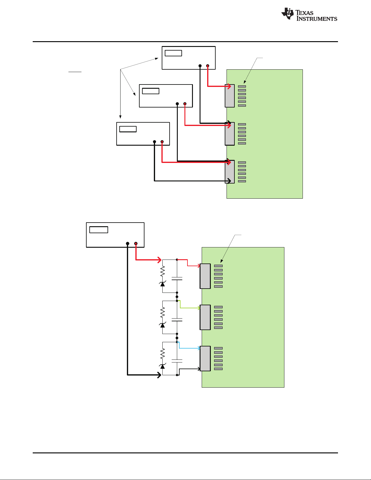
3.2.2 Use with ~12-26VDC Power Supply
Important: Install jumpers JP1-18 (18) located near the black battery connectors P1-P3 before connecting
power supplies. These jumpers connect a precision 0.1% resistor divider network between cell
connections.
Connect an appropriate power supply capable of supplying 12-26VDC to connector P1, then plug P1 into
the EVM connector. Any voltage which meets the IC requirements will work, 18-24V is typical of most
six-cell systems. Plug additional supplies into P2 and P3. The supplies must be isolated from each other
and from earth ground to avoid unintentional short circuits. A separate supply is required for each IC
(each cell-connection plug).
The supply negative connection is made to pin 1 of the mating connector, the pin that will connect to the
bottom-most pin of the mating connector. The positive connection is made to pin 7, the top-most on the
connector. It is not necessary to connect to the intermediate pins due to the resistive divider on the EVM
which was enabled when JP1-18 were installed
Do not remove any of the jumpers JP1-18 while using the EVM in this
configuration. Lethal DC voltages may be present for these configurations.
Contact with these voltages may result in serious injury or death. Use
appropriate safety precautions.
EVM Assembly and Configuration
CAUTION
SLUU437B–October 2010– Revised May 2011 bq76PL536 EVM Quick Start Guide
Submit Documentation Feedback
Copyright © 2010–2011, Texas Instruments Incorporated
3
Page 4
P1
P2
P3
+
–
Power Supply
+
–
20V
20V
Power Supply
+
–
Power Supply
Bq76pl536
EVM-3
Jumpers
Installed
(+) and (–) outputs
must
remain isolated
from earth ground .
20V
P1
P2
P3
+
–
54V
Power Supply
Bq76pl536
EVM-3
Jumpers
Installed
10Ω
2W
18V
220µF
63V
+
10Ω
2W
18V
220µF
63V
+
10Ω
2W
18V
220µF
63V
+
54V
EVM Assembly and Configuration
Figure 1. Correct Connection of Three ~20V Power Supplies to EVM
www.ti.com
4
bq76PL536 EVM Quick Start Guide SLUU437B–October 2010– Revised May 2011
Figure 2. Alternate Connection for Single 54V Supply
Copyright © 2010–2011, Texas Instruments Incorporated
Submit Documentation Feedback
Page 5
P1
P2
P3
+
–
60V
Power Supply
Bq76pl536
EVM-3
Jumpers
Installed
Resistor divider
(18K) does not
supply sufficient
current to IC’s
Base IC must be
powered!
P1
P2
P3
+
–
60V
Power Supply
Bq76pl536
EVM-3
Jumpers
Installed
Resistor divider
(18K) does not
supply sufficient
current to IC’s
P1
P2
P3
+
–
60V
Power Supply
Bq76pl536
EVM-3
Jumpers
Installed
Resistor divider
(18K) does not
supply sufficient
current to IC’s
www.ti.com
EVM Assembly and Configuration
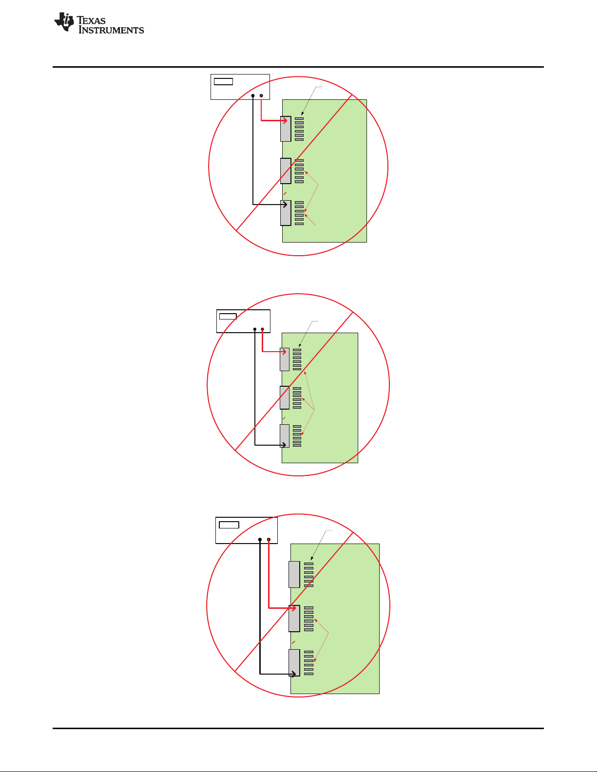
Figure 3. Incorrect Connections, Base IC Not Powered
Figure 4. Incorrect Connections, Insufficient V
SLUU437B–October 2010– Revised May 2011 bq76PL536 EVM Quick Start Guide
Submit Documentation Feedback
Figure 5. Incorrect Connections, Top IC Not Powered, IC1,2 Insufficient V
Copyright © 2010–2011, Texas Instruments Incorporated
BAT
Per IC
BAT
5
Page 6
Connecting the EVM
3.3 Non-Critical Hardware Testing or Firmware Development
3.3.1 Stacking EVMs
For casual testing, one or two devices may be powered (in order from negative to positive) in lieu of
powering all 3 devices. Due to poor termination of the unpowered devices in this configuration, detailed
testing or critical hardware evaluations should not be undertaken. Any odd behavior or unexpected fault
conditions should be ignored until verified with the EVM correctly powered by three isolated supplies
4 Connecting the EVM
4.1 Connection Order
www.ti.com
(a) Configure the EVM jumpers per Section 3.1.
(b) Connect the EVM to the Power Supplies or cells, turn on the supplies at ~12 to 24V is recommended.
The Absolute Maximum voltage per IC is 36V and should not be exceeded, 30V is the recommended
maximum continuous voltage.
(c) Connect the USB cable to the Aardvark and your PC.
(d) Connect the Aardvark ribbon cable to the 10 pin header on the EVM board
The Aardvark adapter should be connected last during power-up, and disconnected first when
powering down. If not using the wall adapter to supply power, it must be after starting the Windows
application to avoid a turn-on issue with the Aardvark adapter. Many laptop computers power off their
USB ports when they go into sleep, standby, or hibernate modes. If the device the Aardvark is
connected to remains powered when this happens, the Aardvark may suffer permanent damage.
(e) Start the WinGUI User Interface software supplied with the EVM and installed earlier
4.2 Connection Notes
The ISO-COMMS section of the EVM board isolates the EVM side voltages completely from the PC side.
It isolates all power, ground, and signal lines to the EVM. Caution must still be carefully taken when using
the EVM as part of a stack, where lethal voltages may be present. The galvanic isolation provided by the
ISO-COMMS section does not eliminate the need for safe handling procedures, proper High-Voltage
equipment and protective clothing. Proper safety procedures should always be followed.
6
bq76PL536 EVM Quick Start Guide SLUU437B–October 2010– Revised May 2011
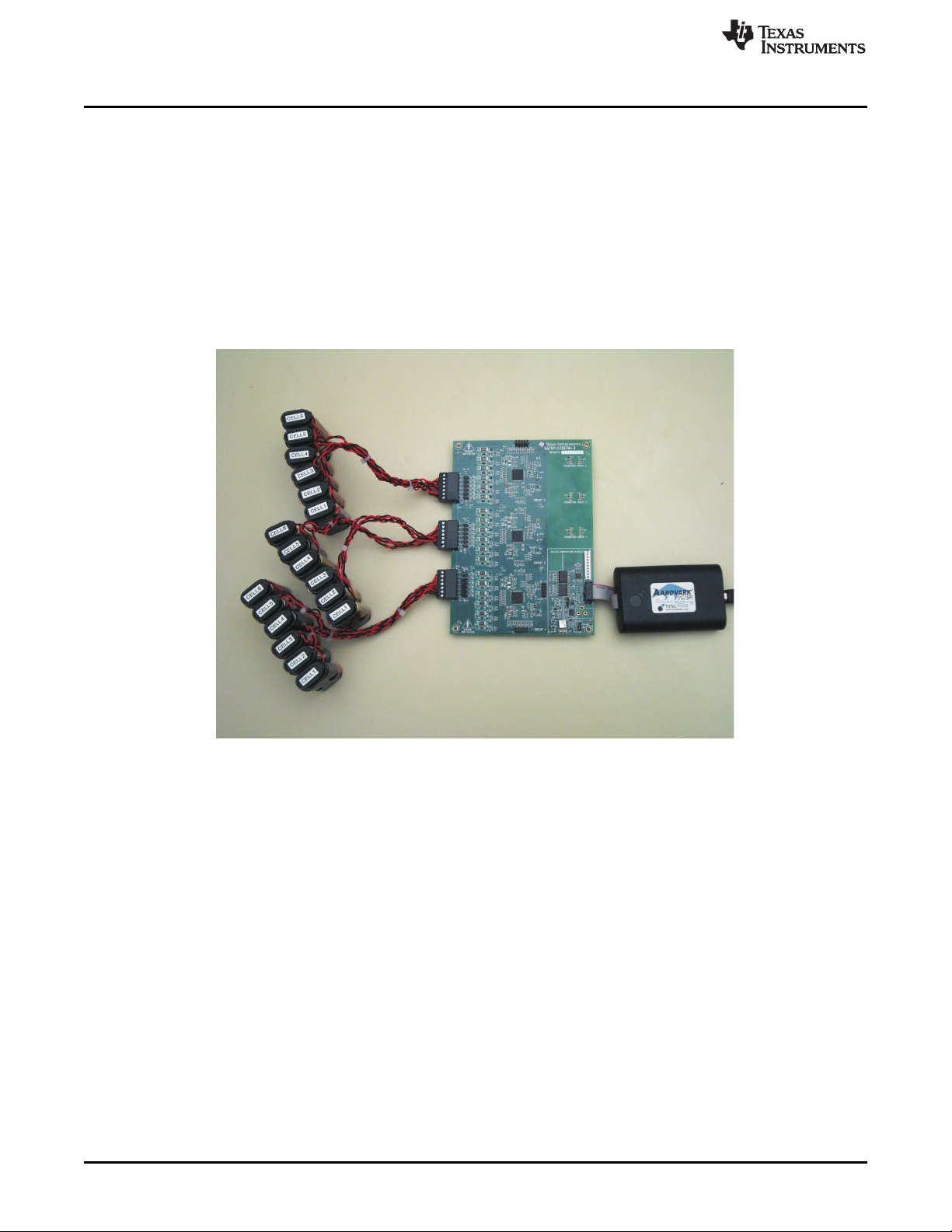
Figure 6. Bq76pl536EVM-3
Copyright © 2010–2011, Texas Instruments Incorporated
Submit Documentation Feedback
Page 7

www.ti.com
Because the ISO-COMMS circuit section fully isolates the PC, Aardvark, and wall adapter from the EVM
“battery” side, the Aardvark is insensitive to the powering of the EVM, which receives its’ power from the
battery cells or power supply used for evaluation.
The grounds (VSS) are fully isolated; please keep this in mind when using an oscilloscope or meter. Do
not inadvertently connect the EVM VSS to the PC/Aardvark VSS by connecting two probe grounds or
otherwise forming a ground loop through external wiring, including the building wiring.
4.3 Quick Check
The first step in communicating with the bq76PL536 is to set a unique address for each device in the
stack. This is required even if you are only using a single device. This occurs automatically when the
Evaluation software is first started. To do this manually, select COMMAND | AUTO ADDRESS (shortcut
key CTRL + A). This will cause the software to interrogate the stack of ‘536 devices, find all available
devices, and assign each a unique address beginning with address 0x01. Address 0x00 is reserved for
un-addressed devices.
After addressing is complete, you should see the number of devices found and the total combined voltage
of all cells being monitoring displayed in the STACK HEIGHT and V STACK windows.
5 Evaluation Software Details
5.1 Main Screen
The main screen is divided into 4 major areas, plus the menu and status bars. The software is referred to
as the “Windows Graphical User Interface”, or abbreviated to WinGUI.
Evaluation Software Details
VBRIC K The voltage measured by the bq76PL536 between the BATx and VSS pins
VCELLn the voltage measured between the pair of pins VCn – VCn-1 (i.e. VCELL2 = VC2 -
VC1).
ADDR displays the address of the device being monitored in the measurement result area.
LOG DEVICE Checking this box will add the contents of the device at this address to the log file.
TSn The voltage measured between the TSn+ and TSn- inputs, converted by the WinGUI
to temperature based on the characteristics of the thermistor used in the EVM design.
The EVM and WinGUI are configured to measure this voltage as a ratio of REG50,
which removes any offset or gain errors introduced by drift in the REG50 output.
VIEW AS... Shows the ratio of the measured input voltage to REG50 as a percentage.
SLUU437B–October 2010– Revised May 2011 bq76PL536 EVM Quick Start Guide
Submit Documentation Feedback
Copyright © 2010–2011, Texas Instruments Incorporated
7
Page 8

Evaluation Software Details
Updates the displayed measurements for this device. The conversion is started by
sending the register command CONVERT[CONV]=1,
or hardware by toggling the CONV pin if the HW IO CONTROL box is checked.
5.1.1 Volatile RAM Configuration Registers –
The lower half of this area displays the volatile configuration registers shown as bit fields, see the
bq76PL536 data sheet for details on programming these registers. These registers display green for logic
0, and orange for logic 1. The two states may be toggled between by left-clicking on the bit
The STATUS, COV_FAULT, and CUV_FAULT bits are either white (logic 0) or red (logic 1) for asserted.
In most cases, the asserted state indicates an error condition sensed by the bq76PL536.
To clear a fault, first remove the physical condition causing the fault, then click on the ALERT or FAULT
bit to reset the state of the bit. This writes a 1 to the bit, followed by a 0, which is the device’s method for
clearing the asserted bit state back to logic 0.
5.1.2 Group-3 Protected Registers –
The device is provided with many configuration options set by bits contained in a special set of registers
protected against accidental writing. These RAM registers are initialized from OTP (One-Time
Programmable) EPROM cells. The device is shipped with these EPROM locations un-programmed
(blank). The Windows GUI interface hides the un-programmed nature of the device by setting defaults in
the registers cells when the Evaluation software starts (this can be defeated by setting the TOOLS |
OPTIONS defaults). The last settings are also automatically saved by the GUI and restored on next use.
These features are provided for ease of use, and are implemented solely in the GUI. Users are
responsible for programming OTP bits in parts correctly during manufacturing for correct operation
in-circuit.
Some Group-3 registers are shown as registers at the bottom of the left side of the screen, the others in
the top right section of the screen as listboxes and registers
www.ti.com
5.1.3 Quick Access
The Quick Access register(s) provide R/W access to any location in the part. They are named arbitrarily in
the GUI ‘X’, ‘Y’, and ‘Z’ – there are no XYZ registers in the part. Some registers, such as the MASTER
register require multi-byte writes to “unlock” the target register for writing. To accomplish this, program the
X register address/data with the first unlock key, the Y register with the second unlock key, and finally the
Z register with the target address and data. Then use the “write all” button to send all three address/data
bytes in the correct order and timing to accomplish the multi-byte write. (This is done automatically when
using the Protected Registers window.)
5.1.4 LED Status Indicators
At the top right of the user interface screen are 8 status indicator "LED's". These provide a quick view of
the status of the devices, and the interface, cable connections, etc. Green normally indicates a logic 0
condition, and red a logic one condition. Gray indicates undefined.
8
bq76PL536 EVM Quick Start Guide SLUU437B–October 2010– Revised May 2011
Copyright © 2010–2011, Texas Instruments Incorporated
Submit Documentation Feedback
Page 9

www.ti.com
ALERT A condition has been sensed that is causing the ALERT hardware pin to be asserted. This
is also indicated by the ALERT bit being set (red) in the [DEVICE] STATUS register. The
source of the ALERT condition is indicated in the ALERT register just below the STATUS
register.
FAULT Similar to the ALERT indicator, this LED indicates the FAULT bit, and FAULT hardware
pin are asserted. The source is indicated in the FAULT register, just below the ALERT
register.
LAST CRC The last CRC received by the GUI was incorrect for the contents of the packet. This
usually indicates a communications error caused by improper connection, excessive
cabling, etc. The cause of the communications error should be corrected before
continuing.
LOG Green if a log file is being written to. Logging is useful to capture information about cell or
interface behavior over long periods of time
STACK At least one device was found during auto-addressing or rebuild addresses. This indicates
that the bottom device in the stack was found, is powered, not in POR, and the ribbon
cable from the Aardvark to the EVM is connected correctly. This verifies the cabling and
connection all the way to the IC.
INTERFACE The Aardvark USB-SPI interface adapter was successfully found and communicated with.
This verifies the cabling and driver to the adapter.
5.1.5 Global Registers
Evaluation Software Details
DEVICE The Address of the device currently being communicated with. Change to access
different devices in the stack. “BROADCAST” mode also available to send a single
command to all devices in the stack. (In BROADCAST mode, no data is shown – the
interface can only display data from one device at a time.
STACK HT. The number of devices found during the last AUTO-ADDRESS or
REBUILD-ADDRESS cycle.
POLL Check or un-check this box to turn polling on or off. Note that many menu items are
unavailable during polling – turn polling off to access them.
RATE This list box allows choosing a polling rate between 100ms and 60s. The LED
illuminates green each time the GUI polls the device stack. Useful as a heartbeat
indicator when polling or logging is active. A setting “Fast” is also available. In this
position, the WinGUI will poll as fast as possible, with only Windows OS slowing it
down. On most systems, this results in a poll every 10-20ms, but your results may vary
depending on the speed of your CPU and other tasks that are running.
LOG STACK Enables or disables data logging. Logging is to a file in comma-separated-values (.csv)
format. Set up logging in the LOG | SETUP menu. Logging may also be started /
stopped under the LOG menu. Data is captured each poll, set by the polling interval in
TOOLS | INTERFACE.
VIEW PLOT Check this box to view a dynamic plot of data collected during polling. See PLOTTING
for further information on configuring the plotter.
SLUU437B–October 2010– Revised May 2011 bq76PL536 EVM Quick Start Guide
Submit Documentation Feedback
Copyright © 2010–2011, Texas Instruments Incorporated
9
Page 10

Evaluation Software Details
HW I/O Check this box to force the Evaluation software to use the hardware pins CONV and
5.2 Addressing
The first step in communicating with the
bq76PL536 is to set a unique address for each
device in the stack. This is required even if you are
only using a single device. On the menu, select
COMMAND | AUTO ADDRESS (shortcut key CTRL
+ A). This will cause the software to interrogate the
stack of '536 devices, find all available devices, and
assign each a unique address beginning with
address 0x01. Address 0x00 is reserved for
un-addressed devices.
After addressing is complete, the number of
devices found and the total combined voltage of all
cells being monitoring are displayed in the STACK
HEIGHT and V STACK windows. In this example, 2
bq76PL536 devices are connected together
monitoring 12 cells of about 3.3V each.
www.ti.com
DRDY to initiate, and monitor ADC conversion cycles, instead of sending commands to
the CONVERT_CTRL[CONV] register bit. Similarly, it is monitoring the FAULT and
ALERT hardware pin states to determine a FAULT and/or ALERT condition being
present. Note that in HW I/O mode, the REFRESH button toggles the hardware CONV
line, but the user may optionally use the CONVERT_CTRL[CONV] bit to force software
initiated conversions by clicking on the bit.
The screen automatically refreshes each time something changes. Addressing the device will cause all
displayed values and registers to update. The user hould see all cell voltages displayed, along with
registers showing FAULT and ALERT status, DEVICE STATUS, etc.
5.3 Menus and Commands
5.3.1 File Menu
This menu provides a way to save complex register
settings between sessions. The settings are saved
to a file on the local disk, selected using a dialog
box that appears when the Load or Save command
is selected. Multiple files, with different settings may
be saved under different file names. Saved register
settings are then re-loaded from the saved file. All
registers – volatile and shadow – are saved or
loaded, except the ADC measurements
Another useful command available in this menu allows copying the current measurement data (VCn,
VBRICK, and TS1, TS2, in that order) to the clipboard, and subsequent copying to a document or
spreadsheet.measurements.
It will also create Eprom programmable image for Bq76PL536 OTP EPROM Programmer
10
bq76PL536 EVM Quick Start Guide SLUU437B–October 2010– Revised May 2011
Copyright © 2010–2011, Texas Instruments Incorporated
Submit Documentation Feedback
Page 11

www.ti.com
5.3.2 Command Menu
RESET allows resetting either the current device,
or the entire stack with one command. (Note: The
stack is reset using a BROADCAST command
packet, whether Broadcast is selected as the
current device or not.)
RELOAD SHADOW REGISTERS will re-initialize
the Group-3 Protected Registers from the OTP
EPROM. This is useful to verify programming.
Because the part is shipped unprogrammed, the result of reloading the shadow registers is to transfer all
zeros to the shadow cells, and will usually result in many ALERTS and FAULTS being triggered which
are normally hidden by the GUI per the OPTION menu settings (see below).
REFRESH updates the screen contents, and is equivalent to the large REFRESH button in the Volatile
registers area.
Evaluation Software Details
SLUU437B–October 2010– Revised May 2011 bq76PL536 EVM Quick Start Guide
Submit Documentation Feedback
Copyright © 2010–2011, Texas Instruments Incorporated
11
Page 12

Evaluation Software Details
5.3.3 Tools Menu
PROGRAM opens a dialog box that programs the
contents of the shadow registers to the OTP
EPROM cells in the bq76PL536. The data
contained in the equivalent address volatile
registers is used as the data source. i.e. the data in
register CONFIG_OT[] is used to program the
EPROM cells which will in turn initialize the
CONFIG_OT[] register at the next RESET.
INTERFACE SETUP opens a dialog box that allows changing the SPI communications speed.
OPTIONS opens a dialog that sets program startup options. These are provided to make the GUI easier
to use, and prevent a slew of alarms (FAULTS and ALERTS) at startup. Programmers wishing to check
their code will want to disable most of these startup niceties during final code checkout. See Packing List
for details of the startup Options.
MEASUREMENT FILTER SETUP opens a listbox that controls filtering of the measurement data. This is
a simple LIFO buffer which is then averaged, producing a running average result. The default value is 1
(no filtering), but it can be set from 1 (no filtering) to 20 (heavy filtering).
COMMUNICATIONS MONITOR opens the SPI-spy text box. All SPI traffic to and from the ‘536 are
copied into this box in an easy to read hex format shown below. When first opened, a warning message
is displayed telling the user that the monitor should only be used for short periods to avoid consuming
too much PC memory. If monitoring traffic for more than a few 10’s of seconds is needed, use the data
logging feature built in to the WinGUI.
www.ti.com
SDO data is data sent from the monitored stack to the PC. SDI is data sent from the PC (WinGUI) to the
stack of ‘536’s. The monitor displays all data sent to and from the stack.
The Communications Monitor box shown in Figure 7 displays an error found in communicating with a
stack. The error shown is normally encountered by the AUTO_ADDRESS algorithm used by the WinGUI
as it attempts to find all addressed devices – this error results from an attempted poll to a device which
does not exist.
12
Figure 7. SPI Monitor Showing Communications Error
bq76PL536 EVM Quick Start Guide SLUU437B–October 2010– Revised May 2011
Copyright © 2010–2011, Texas Instruments Incorporated
Submit Documentation Feedback
Page 13

www.ti.com
6 Startup Options Dialog
This dialog controls whether or not the WinGUI sets certain options and registers at startup. If a Group-3
register value is affected, it is done by the WinGUI writing the new value to the RAM register after the
POR period; the value is not written to the OTP-EPROM. OTP-EPROM is normally shipped blank from the
factory. Overwriting these RAM registers at startup prevents many FAULT and ALERT bits from triggering
at startup, and is done as a user convenience.
The option checkboxes are shown below in the state the WinGUI is shipped in. If the user changes any
checkbox states, the new defaults are saved automatically when the WinGUI exits.
Startup Options Dialog
BROADCAST MODE when checked, brings up the interface set to broadcast
messages to all devices, no data is shown. In broadcast mode, the WinGUI does
not know which device to read, so no register data is displayed.
If this box is not checked, the interface comes up ready to read/write device 1.
SET COV […] sets the COV threshold to 5.0V, its highest value
DISABLE COV sets the CONFIG_COV[DISABLE] bit, disabling COV FAULTs
DISABLE CUV sets the CONFIG_CUV[DISABLE] bit, disabling CUV ALERTs
CLEAR LATCHED BITS clears all FAULT and ALERT bits latched in the FAULT and ALERT registers,
which may have otherwise normally been set by startup conditions, i.e. Power-On-Reset
ENABLE VBRICK sets the ADC_CONTROL[GPAI] and FUNC_CONFIG[GPAI_SRC] bits. This causes
the VBRICK value (BAT-VSS) to be measured on each conversion cycle.
READ ALL VOLTAGES sets the bits ADC_CTRL[CS2:0] to 101b to convert all VCn inputs at each
conversion request
READ ALL TEMPERATURES sets the bits ADC_CTRL[TS2:1) to convert both thermistor TSn) inputs at
each conversion cycle. It also sets the bits IO_CTRL[TS2:1] to turn on the thermistor power
DYNAMICALLY CONTROL ADC_ON sets the bits FUNC_CONFIG[ADCT1:0] to the value 01b,
changing the conversion timing from the default 3µs to 6µs. The 6µs setting is recommended for best
accuracy. This checkbox also causes the GUI to set the ADC_CTRL[ADC_ON] bit before each
conversion, convert, then set the ADC_ON bit back to 0. This is done around each conversion request,
whether hardware or software
SLUU437B–October 2010– Revised May 2011 bq76PL536 EVM Quick Start Guide
Submit Documentation Feedback
Copyright © 2010–2011, Texas Instruments Incorporated
13
Page 14
PLOTTING
LOAD REGISTER FILE will cause the registers to be pre-loaded with the contents of the file named in
the box. This file should be the one saved by the File | Save Registers menu selection. This feature can
be used to quickly reload a specific configuration back to the devices under test.
BLINK LED’S causes the LED indicators in the Global Registers area to blink. If not checked, they stay
illuminated RED under error conditions.
APPLY FILTER must be checked for the filtering available in the Tools menu to be operable. When
un-checked, the filter is off (set to 1). Newer versions of the WinGUI (2.1.12 and later) have deleted this
option, the filter is controlled directly (and only) from the Tools | Filter menu.
7 PLOTTING
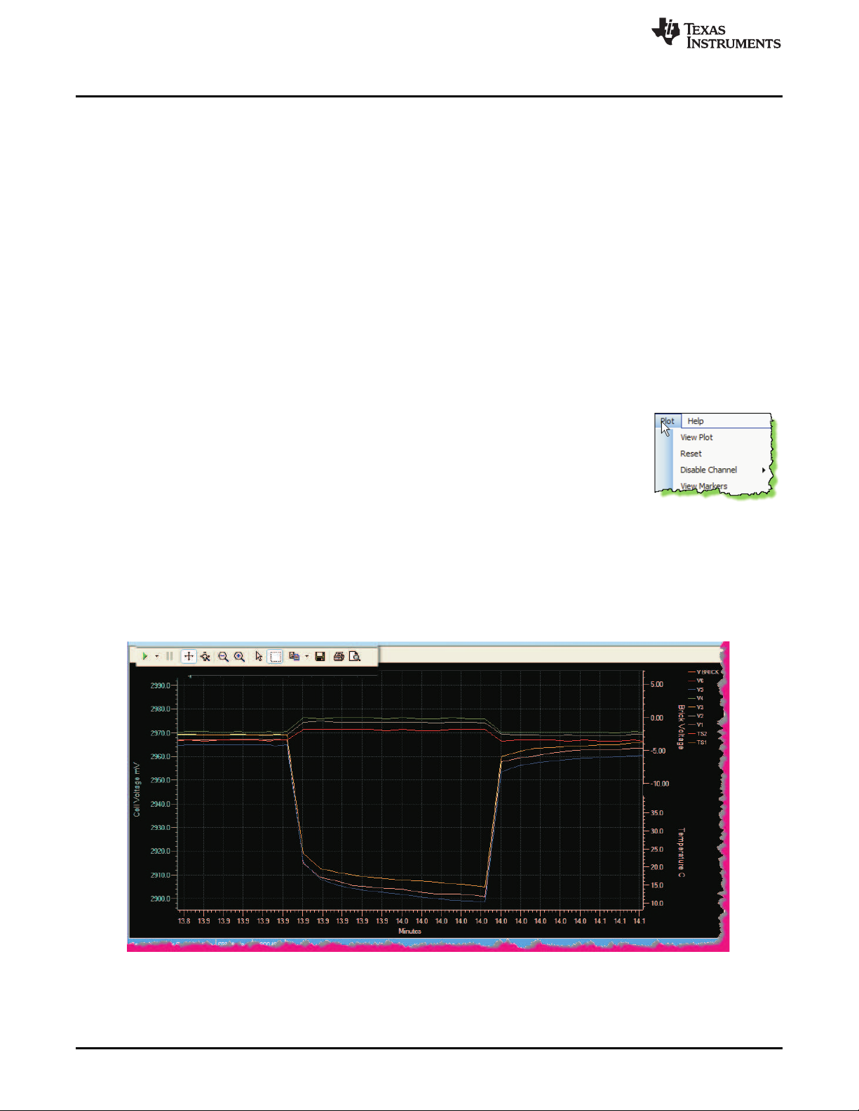
7.1 PLOT MENU
The plot menu allows setting up a simple strip-chart recorder for simple data captures. The data captured
to the plot is not automatically captured in a log file. It is available for use or saving in a variety of formats
while the program is running. The plotted data is lost if the program is exited without saving. Logged data
is preserved in a file.
VIEW PLOT replaces the registers display with the plotter view. It is identical to
checking the “View Plot” checkbox in the GLOBAL REGISTERS / LED display area.
www.ti.com
RESET completely resets the plotter interface, restoring display defaults and clearing all stored data.
DISABLE CHANNEL opens another menu level and allows removal of data channels from the plot.
VIEW MARKERS displays a tick at each poll, helping to distinguish polls which return invalid or corrupt
data from successful polls.
7.2 Plot View
14
Figure 8. Magnified Window View of the Effect of Cell Balancing for Cells 1-3-5.
bq76PL536 EVM Quick Start Guide SLUU437B–October 2010– Revised May 2011
Copyright © 2010–2011, Texas Instruments Incorporated
Submit Documentation Feedback
Page 15

www.ti.com
7.3 Plotter Controls
Plotter controls are shown slightly magnified in the upper left of the capture above. From the left, they
control:
PLOTTING
RESUME TRACKING - causes the strip-chart to resume automatically tracking
changes in voltage, time, or temperature – in other words, resume auto-ranging. This
green arrow is illuminated after manually zooming in or opening a window in the
default view. The default is auto-ranging is enabled. The small black down-arrow
opens a small menu of selections controlling the automatic tracking. Whether
displayed or not, data is always captured on each poll refresh.
PAUSE DISPLAY – momentarily stops auto-tracking. To resume, use the RESUME
TRACKING button described above.
SCROLL X-Y – After clicking this control, the display (data) window can be moved by
left-clicking the mouse button in the display and moving the mouse. Use RESUME
TRACKING to restore the display. Each data set (VCn voltages, VBRICK, temperature,
time) scale can be individually moved by clicking and holding the left mouse button on
the units field and scrolling up-down or left-right (time scale).
EXPAND X-Y – This control allows zooming in or out on the displayed scale. Choose
this button, then click and hold the left mouse button to operate. Each data set (VCn
voltages, VBRICK, temperature, time) scale can be individually zoomed by clicking and
holding the left mouse button on the units field and scrolling up-down or left-right (time
scale).
ZOOM OUT – click on a scale, then click this button to move out in incremental steps.
ZOOM IN – similar but opposite action to Zoom out, above.
SELECT – allows selecting data or scales (opposite of window mode, described next)
WINDOW – click this button, then drag a zoom box around an area in the display to
zoom in. This mode is canceled by clicking on the SELECT arrow described above.
The display is restored by using the TRACKING RESUME button, above.
COPY TO CLIPBOARD – the data is copied to the clipboard for inclusion in a
document or spreadsheet. A small menu allows selecting the numeric data to copy, or
the graphic.
SAVE – the graphic to a .PNG file
PRINT – the graphic to a printer
PRINT PREVIEW – see what the graphic will look like on your printer before printing.
SLUU437B–October 2010– Revised May 2011 bq76PL536 EVM Quick Start Guide
Submit Documentation Feedback
Copyright © 2010–2011, Texas Instruments Incorporated
15
Page 16

Support
8 Support
Contact the local TI sales office for technical support. Support is also available through the TI E2E™
community forum at http://e2e.ti.com/support/power_management/default.aspx
TI's Engineer-to-Engineer (E2E) Community. Created to foster collaboration among engineers. At
e2e.ti.com, you can ask questions, share knowledge, explore ideas and help solve problems with fellow
engineers.
9 Packing List
Line Quantity Each Description
1 1 ea Bq76pl536Evm-3 RevX EVM PCB assembly (x = rev level)
2 1 ea Aardvark adapter USB→SPI (FW Rev 3.41 or later required)
3 1 ea USB cable, 1m
4 3 ea Mating battery connector, 7 pos receptacle
7 20 ea 2 pin jumpers, .025” post, 0.10” cntr
8 1 ea CD-ROM containing software and documentation
www.ti.com
16
bq76PL536 EVM Quick Start Guide SLUU437B–October 2010– Revised May 2011
Copyright © 2010–2011, Texas Instruments Incorporated
Submit Documentation Feedback
Page 17

Evaluation Board/Kit Important Notice
Texas Instruments (TI) provides the enclosed product(s) under the following conditions:
This evaluation board/kit is intended for use for ENGINEERING DEVELOPMENT, DEMONSTRATION, OR EVALUATION
PURPOSES ONLY and is not considered by TI to be a finished end-product fit for general consumer use. Persons handling the
product(s) must have electronics training and observe good engineering practice standards. As such, the goods being provided are
not intended to be complete in terms of required design-, marketing-, and/or manufacturing-related protective considerations,
including product safety and environmental measures typically found in end products that incorporate such semiconductor
components or circuit boards. This evaluation board/kit does not fall within the scope of the European Union directives regarding
electromagnetic compatibility, restricted substances (RoHS), recycling (WEEE), FCC, CE or UL, and therefore may not meet the
technical requirements of these directives or other related directives.
Should this evaluation board/kit not meet the specifications indicated in the User’s Guide, the board/kit may be returned within 30
days from the date of delivery for a full refund. THE FOREGOING WARRANTY IS THE EXCLUSIVE WARRANTY MADE BY
SELLER TO BUYER AND IS IN LIEU OF ALL OTHER WARRANTIES, EXPRESSED, IMPLIED, OR STATUTORY, INCLUDING
ANY WARRANTY OF MERCHANTABILITY OR FITNESS FOR ANY PARTICULAR PURPOSE.
The user assumes all responsibility and liability for proper and safe handling of the goods. Further, the user indemnifies TI from all
claims arising from the handling or use of the goods. Due to the open construction of the product, it is the user’s responsibility to
take any and all appropriate precautions with regard to electrostatic discharge.
EXCEPT TO THE EXTENT OF THE INDEMNITY SET FORTH ABOVE, NEITHER PARTY SHALL BE LIABLE TO THE OTHER
FOR ANY INDIRECT, SPECIAL, INCIDENTAL, OR CONSEQUENTIAL DAMAGES.
TI currently deals with a variety of customers for products, and therefore our arrangement with the user is not exclusive.
TI assumes no liability for applications assistance, customer product design, software performance, or infringement of
patents or services described herein.
Please read the User’s Guide and, specifically, the Warnings and Restrictions notice in the User’s Guide prior to handling the
product. This notice contains important safety information about temperatures and voltages. For additional information on TI’s
environmental and/or safety programs, please contact the TI application engineer or visit www.ti.com/esh.
No license is granted under any patent right or other intellectual property right of TI covering or relating to any machine, process, or
combination in which such TI products or services might be or are used.
FCC Warning
This evaluation board/kit is intended for use for ENGINEERING DEVELOPMENT, DEMONSTRATION, OR EVALUATION
PURPOSES ONLY and is not considered by TI to be a finished end-product fit for general consumer use. It generates, uses, and
can radiate radio frequency energy and has not been tested for compliance with the limits of computing devices pursuant to part 15
of FCC rules, which are designed to provide reasonable protection against radio frequency interference. Operation of this
equipment in other environments may cause interference with radio communications, in which case the user at his own expense
will be required to take whatever measures may be required to correct this interference.
EVM Warnings and Restrictions
It is important to operate this EVM within the input voltage range of 7V to 36V and the output voltage range of 7V to 35V .
Exceeding the specified input range may cause unexpected operation and/or irreversible damage to the EVM. If there are
questions concerning the input range, please contact a TI field representative prior to connecting the input power.
Applying loads outside of the specified output range may result in unintended operation and/or possible permanent damage to the
EVM. Please consult the EVM User's Guide prior to connecting any load to the EVM output. If there is uncertainty as to the load
specification, please contact a TI field representative.
During normal operation, some circuit components may have case temperatures greater than 85°C. The EVM is designed to
operate properly with certain components above 85°C as long as the input and output ranges are maintained. These components
include but are not limited to linear regulators, switching transistors, pass transistors, and current sense resistors. These types of
devices can be identified using the EVM schematic located in the EVM User's Guide. When placing measurement probes near
these devices during operation, please be aware that these devices may be very warm to the touch.
Mailing Address: Texas Instruments, Post Office Box 655303, Dallas, Texas 75265
Copyright © 2011, Texas Instruments Incorporated
Page 18

IMPORTANT NOTICE
Texas Instruments Incorporated and its subsidiaries (TI) reserve the right to make corrections, modifications, enhancements, improvements,
and other changes to its products and services at any time and to discontinue any product or service without notice. Customers should
obtain the latest relevant information before placing orders and should verify that such information is current and complete. All products are
sold subject to TI’s terms and conditions of sale supplied at the time of order acknowledgment.
TI warrants performance of its hardware products to the specifications applicable at the time of sale in accordance with TI’s standard
warranty. Testing and other quality control techniques are used to the extent TI deems necessary to support this warranty. Except where
mandated by government requirements, testing of all parameters of each product is not necessarily performed.
TI assumes no liability for applications assistance or customer product design. Customers are responsible for their products and
applications using TI components. To minimize the risks associated with customer products and applications, customers should provide
adequate design and operating safeguards.
TI does not warrant or represent that any license, either express or implied, is granted under any TI patent right, copyright, mask work right,
or other TI intellectual property right relating to any combination, machine, or process in which TI products or services are used. Information
published by TI regarding third-party products or services does not constitute a license from TI to use such products or services or a
warranty or endorsement thereof. Use of such information may require a license from a third party under the patents or other intellectual
property of the third party, or a license from TI under the patents or other intellectual property of TI.
Reproduction of TI information in TI data books or data sheets is permissible only if reproduction is without alteration and is accompanied
by all associated warranties, conditions, limitations, and notices. Reproduction of this information with alteration is an unfair and deceptive
business practice. TI is not responsible or liable for such altered documentation. Information of third parties may be subject to additional
restrictions.
Resale of TI products or services with statements different from or beyond the parameters stated by TI for that product or service voids all
express and any implied warranties for the associated TI product or service and is an unfair and deceptive business practice. TI is not
responsible or liable for any such statements.
TI products are not authorized for use in safety-critical applications (such as life support) where a failure of the TI product would reasonably
be expected to cause severe personal injury or death, unless officers of the parties have executed an agreement specifically governing
such use. Buyers represent that they have all necessary expertise in the safety and regulatory ramifications of their applications, and
acknowledge and agree that they are solely responsible for all legal, regulatory and safety-related requirements concerning their products
and any use of TI products in such safety-critical applications, notwithstanding any applications-related information or support that may be
provided by TI. Further, Buyers must fully indemnify TI and its representatives against any damages arising out of the use of TI products in
such safety-critical applications.
TI products are neither designed nor intended for use in military/aerospace applications or environments unless the TI products are
specifically designated by TI as military-grade or "enhanced plastic." Only products designated by TI as military-grade meet military
specifications. Buyers acknowledge and agree that any such use of TI products which TI has not designated as military-grade is solely at
the Buyer's risk, and that they are solely responsible for compliance with all legal and regulatory requirements in connection with such use.
TI products are neither designed nor intended for use in automotive applications or environments unless the specific TI products are
designated by TI as compliant with ISO/TS 16949 requirements. Buyers acknowledge and agree that, if they use any non-designated
products in automotive applications, TI will not be responsible for any failure to meet such requirements.
Following are URLs where you can obtain information on other Texas Instruments products and application solutions:
Products Applications
Audio www.ti.com/audio Communications and Telecom www.ti.com/communications
Amplifiers amplifier.ti.com Computers and Peripherals www.ti.com/computers
Data Converters dataconverter.ti.com Consumer Electronics www.ti.com/consumer-apps
DLP® Products www.dlp.com Energy and Lighting www.ti.com/energy
DSP dsp.ti.com Industrial www.ti.com/industrial
Clocks and Timers www.ti.com/clocks Medical www.ti.com/medical
Interface interface.ti.com Security www.ti.com/security
Logic logic.ti.com Space, Avionics and Defense www.ti.com/space-avionics-defense
Power Mgmt power.ti.com Transportation and www.ti.com/automotive
Microcontrollers microcontroller.ti.com Video and Imaging www.ti.com/video
RFID www.ti-rfid.com Wireless www.ti.com/wireless-apps
RF/IF and ZigBee® Solutions www.ti.com/lprf
TI E2E Community Home Page e2e.ti.com
Automotive
Mailing Address: Texas Instruments, Post Office Box 655303, Dallas, Texas 75265
Copyright © 2011, Texas Instruments Incorporated
Page 19

Mouser Electronics
Authorized Distributor
Click to View Pricing, Inventory, Delivery & Lifecycle Information:
Texas Instruments:
BQ76PL536EVM-3
 Loading...