

Page 1

User's Guide
SLVU924B–March 2014–Revised April 2014
bq76920 Evaluation Module User's Guide
The bq76920EVM evaluation module (EVM) is a complete evaluation system for the bq76920, a 3-cell to
5-cell Li-Ion battery analog front end (AFE) integrated circuit. The EVM consists of a bq76920 circuit
module which is used for simple evaluation of the bq76920 functions. The circuit module includes one
bq76920 integrated circuit (IC), sense resistor, power FETs, and all other onboard components necessary
to protect the cells from overcharge, over discharge, short circuit, and overcurrent discharge in a 5-series
cell Li-Ion or Li-Polymer battery pack. The circuit module connects directly across the cells in a battery.
With a compatible interface board and Microsoft®Windows®based PC graphical user interface (GUI)
software, the user can view the bq76920 registers, adjust protection limits and enable FET control outputs.
Contents
1 Features....................................................................................................................... 2
1.1 Kit Contents.......................................................................................................... 2
1.2 Ordering Information ............................................................................................... 2
1.3 bq76920 Circuit Module Performance Specification Summary............................................... 3
1.4 Required Equipment................................................................................................ 3
2 bq76920 EVM Quick Start Guide.......................................................................................... 3
2.1 Before You Begin................................................................................................... 3
2.2 Quick Start........................................................................................................... 4
3 bq76940/bq76930/bq76920 Software .................................................................................... 5
3.1 System Requirements.............................................................................................. 5
3.2 Installing the bq76940/bq76930/bq76920 Software ........................................................... 5
3.3 Interface Adapter.................................................................................................... 5
3.4 Software Operation................................................................................................. 6
4 bq76920 Circuit Module Use.............................................................................................. 11
4.1 Cell Simulator...................................................................................................... 11
4.2 Evaluating with Simulated Current.............................................................................. 11
4.3 Reducing the Cell Count ......................................................................................... 12
4.4 Connecting Cells .................................................................................................. 13
4.5 Connecting to a Host ............................................................................................. 13
4.6 Gauge Circuits..................................................................................................... 13
4.7 Unused Components ............................................................................................. 13
5 bq76920EVM Circuit Module Physical Construction................................................................... 15
5.1 Board Layout....................................................................................................... 15
5.2 Bill of Materials .................................................................................................... 23
6 Related Documents From Texas Instruments.......................................................................... 29
1 EVM Connection for Basic Operation..................................................................................... 5
2 bq76940/bq76930/bq76920 Evaluation Software Display.............................................................. 6
3 Registers View ............................................................................................................... 8
4 I2C Pro View ................................................................................................................. 9
5 Sequence View............................................................................................................. 10
6 Simulating Current Setup.................................................................................................. 12
7 Top Silk Screen............................................................................................................. 15
8 Top Assembly............................................................................................................... 16
Microsoft, Windows are registered trademarks of Microsoft Corporation.
SLVU924B–March 2014–Revised April 2014 bq76920 Evaluation Module User's Guide
Submit Documentation Feedback
List of Figures
1
Copyright © 2014, Texas Instruments Incorporated
Page 2

Features
9 Top Layer.................................................................................................................... 17
10 Layer 2....................................................................................................................... 18
11 Layer 3....................................................................................................................... 19
12 Bottom Layer................................................................................................................ 20
13 Bottom Silk Screen......................................................................................................... 21
14 Bottom Assembly........................................................................................................... 22
15 Schematic Diagram AFE .................................................................................................. 26
16 Schematic Diagram Gauge .............................................................................................. 27
17 Schematic Diagram Cell Simulator ...................................................................................... 28
1 Ordering Information ........................................................................................................ 2
2 Performance Specification Summary ..................................................................................... 3
3 Reducing cell count ........................................................................................................ 12
4 bq76920 Circuit Module Bill of Materials................................................................................ 23
1 Features
• Complete evaluation system for the bq76920 3-cell to 5-cell Li-Ion and Li-Polymer battery AFE
• Populated circuit module for 5-cell configuration for quick setup
• Power connections available on banana jacks
• Communication signals available on 4-pin connector
• Resistor cell simulator for quick setup with only a power supply
• PC software available for configuration
www.ti.com
List of Tables
1.1 Kit Contents
• bq76920 circuit module
• Cable to connect the EVM to an EV2400 or EV2300 interface board
1.2 Ordering Information
For complete ordering information, refer to the product folder at www.ti.com.
EVM Part Number Chemistry Configuration Capacity
bq76920EVM Li-Ion 5 cells Any
NOTE: Although capacity is shown as Any, practical limits of the physical construction of the module
typically limits the operation of the EVM to a 1P or 2P battery construction. Refer to the
physical construction section for board details.
Table 1. Ordering Information
2
bq76920 Evaluation Module User's Guide SLVU924B–March 2014–Revised April 2014
Copyright © 2014, Texas Instruments Incorporated
Submit Documentation Feedback
Page 3
!
www.ti.com
1.3 bq76920 Circuit Module Performance Specification Summary
This section summarizes the performance specifications of the bq76920 circuit module in its default 5-cell
parallel FET configuration.
Typical voltage depends on the number of cells configured. Typical current depends on the application.
Board cooling may be required for continuous operation at or below maximum current.
Table 2. Performance Specification Summary
Specification Min Typ Max Unit
Input voltage BATT+ with respect to BATT– 6 – 25 V
Continuous charge or discharge current 0 – 15 A
Operating temperature range 20 25 30 °C
1.4 Required Equipment
The following equipment is required to operate the bq76920 EVM in a simple demonstration:
• DC power supply, 0–25 V at 0.5 A
• DC voltmeter
• TI EV2300 or EV2400 interface board
• Computer with USB port and compatible Windows operating system and access to the internet
• TI bq76940/bq76930/bq76920 Evaluation Software (see Section 3)
• Test leads to connect equipment
• Electronic load or assorted resistors
Additional equipment may be desired to operate the bq76920 with a more extensive demonstration.
Features
2 bq76920 EVM Quick Start Guide
2.1 Before You Begin
The following warnings and cautions are noted for the safety of anyone using or working close to the
bq76920 EVM. Observe all safety precautions.
Warning The bq76920EVM circuit module may become hot during
Caution Do not leave the EVM powered when unattended.
The circuit module has signal traces, components, and component leads on the
bottom of the board. This may result in exposed voltages, hot surfaces or sharp
edges. Do not reach under the board during operation.
operation due to dissipation of heat. Avoid contact with the
board. Follow all applicable safety procedures applicable to
your laboratory.
CAUTION
SLVU924B–March 2014–Revised April 2014 bq76920 Evaluation Module User's Guide
Submit Documentation Feedback
3
Copyright © 2014, Texas Instruments Incorporated
Page 4

bq76920 EVM Quick Start Guide
The circuit module may be damaged by over temperature. To avoid damage,
monitor the temperature during evaluation and provide cooling, as needed, for
your system environment.
Some power supplies can be damaged by application of external voltages. If
using more than 1 power supply, check your equipment requirements and use
blocking diodes or other isolation techniques, as needed, to prevent damage to
your equipment.
The communication interface is not isolated on the EVM. Be sure no ground
potential exists between the computer and the EVM. Also be aware that the
computer is referenced to the Battery- potential of the EVM.
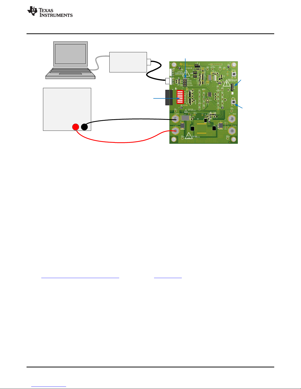
2.2 Quick Start
These steps describe quick connection of the bq76920 EVM to demonstrate operation of the AFE portion
of the EVM. For more detailed descriptions, refer to other sections of the user guide.
Refer to Figure 1 for the following steps.
1. Install the bq76940/bq76930/bq76920 evaluation software. Software is obtained from www.ti.com.
Install drivers for the EV2300, if necessary.
2. Remove shunts from headers connecting the AFE to the gauge.
3. If the EV2300 is used, install shunts on the SCL and SDA pull-up headers. Remove any pull-up shunts
when using the EV2400.
4. Close all dip switch positions (default is closed).
5. Attach the interface board communication adapter to the PC using USB cable. The EV2400 is
recommended, the EV2300 works if it is available and drivers are installed.
6. Attach the interface board I2C connector to the EVM I2C connector using the 4-pin cable.
7. Connect a 0-V DC power supply capable of 250 mA minimum to the “BATT” terminals and adjust to
approximately 18 V.
8. Press and release the BOOT switch.
9. Start the bq769X0 evaluation software. The GUI should display. Click on the Scan box to enable
repeated update of the display. The power supply may be adjusted within range of the part to observe
voltage changes in the GUI display Stack V/T/I section.
10. Set the voltage to approximately 18 V or a mid-range operating level. Clear any faults present by
clicking on the Clear Faults button of the All Read/Write Registers section of the GUI.
11. Click on the Continuous button in the GUI Coulomb Counter section. Enable the CHG_ON and
DSG_ON bits by clicking on the bit and commit the changes. Apply a load to the PACK terminals. Load
current must be within the capability of the supply and the components installed or 15 A, whichever is
lower. Observe the Coulomb Counter value change in the GUI display Stack V/T/I section.
12. Make other adjustments as desired, for evaluation.
Refer to other sections of this user guide for additional details.
www.ti.com
CAUTION
CAUTION
CAUTION
4
bq76920 Evaluation Module User's Guide SLVU924B–March 2014–Revised April 2014
Copyright © 2014, Texas Instruments Incorporated
Submit Documentation Feedback
Page 5
DC Power Supply
+ -
Boot
switch
EV2300/
EV2400
I2C
SMB
Pull-ups
for
EV2300
Remove
for
EV2400
Remove gauge
shunts
Cell simulator
switches on for
power supply
www.ti.com
Figure 1. EVM Connection for Basic Operation
3 bq76940/bq76930/bq76920 Software
This section describes how to install and use the bq76940/bq76930/bq76920 software for the EVM.
The bq76940/bq76930/bq76920 software supports the bq76920 AFE I2C communication. This software is
intended to demonstrate register control and operation of the bq769x0 family of AFEs in the absence of a
gauge or MCU. This software is not intended to operate on a bus with another master. The AFE does not
turn on the protection FETs without control, the bq76940/bq76930/bq76920 software provides that control
from the GUI.
The software may also be identified as bq76940 or bq769X0 in menus or windows as space permits.
bq76940/bq76930/bq76920 Software
3.1 System Requirements
The bq76940/bq76930/bq76920 software requires a Windows 7, or later operating system. The computer
must also have Microsoft®.NET connection software version 4.0, or higher, installed. The examples in this
document are from Windows 7.
3.2 Installing the bq76940/bq76930/bq76920 Software
Find the latest software version in the software section of the EVM tool folder
http://www.ti.com/tool/bq76920EVM or search from power.ti.com. Check periodically for software updates.
Use the following steps to install the bq76940/bq76930/bq76920 software:
1. Copy the archive file to a directory of your choice, extract all files and run the setup.exe application.
2. Follow the instructions and make selections as required on the setup windows selecting Next, as
required. TI recommends installing the software in the default location.
3. On the last window, select Close to complete the bq76940/bq76930/bq76920 software installation.
3.3 Interface Adapter
The bq76940/bq76930/bq76920 evaluation software supports either the TI EV2300 or EV2400 interface
board to provide communication with the EVM board from the computer. Drivers must be installed for the
EV2300. The EV2400 uses operating system drivers and no separate installation is required. Do not
connect the EV2300 interface board to the computer until after the drivers are installed.
SLVU924B–March 2014–Revised April 2014 bq76920 Evaluation Module User's Guide
Submit Documentation Feedback
5
Copyright © 2014, Texas Instruments Incorporated
Page 6
bq76940/bq76930/bq76920 Software
If you have used an EV2300 with your computer previously, no additional installation is required. EV2300
drivers are included in the installation package and are found in the installation directory after installing the
software, typically at c:\Program Files (x86)\Texas Instruments\bq76940. Drivers are found at
http://e2e.ti.com/support/power_management/battery_management/m/videos__files/458983.aspx or
http://www.ti.com/tool/ev2300. Install the drivers by following these steps:
1. Navigate to the installation directory, typically C:\Program Files (x86)\Texas Instruments\bq76940
2. Run the file InstallEV2300Drivers.exe
The interface adapter should not be connected to the I2C connector if a gauge or MCU is connected to
the bus. Board pull-up shunts must be installed for the EV2300 and removed for the EV2400
3.4 Software Operation
This section describes connection of the communication interface to the EVM and operation of the
software.
Although the software runs without connection to a powered device, it is recommended to have the device
on when starting the software. Follow the directions in the quick start section. Figure 1 shows connections
for operation with the GUI software.
Start the software from the desktop shortcut bq769X0 Evaluation Software or the menu Start → All
Programs → Texas Instruments → bq769X0 Eval Software.
When started, the software looks for the communication interface and the device. If either is not found, a
popup window appears and must be acknowledged. When communication is established with the device,
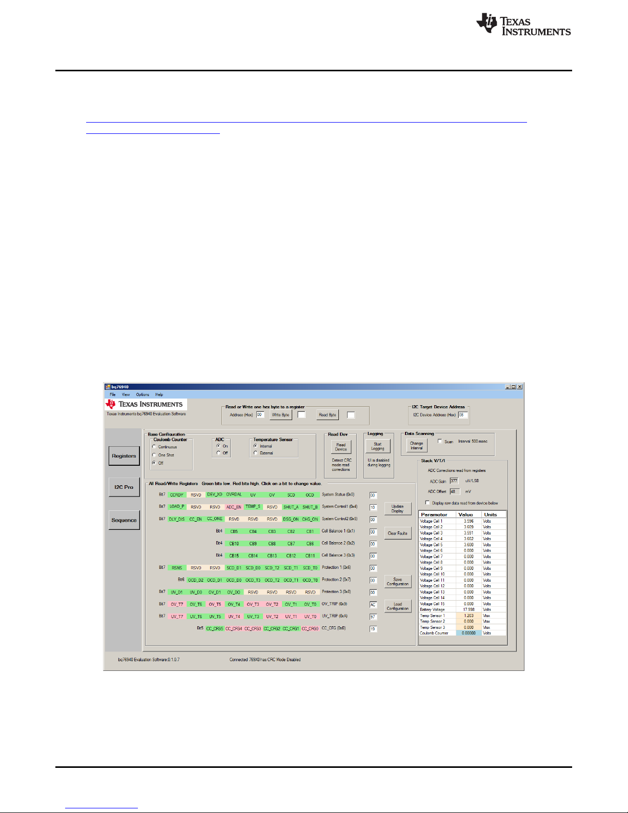
the main window appears as shown in Figure 2.
The bq76940/bq76930/bq76920 software uses popup help tips on many of the control features.
www.ti.com
Figure 2. bq76940/bq76930/bq76920 Evaluation Software Display
The software window contains a menu bar and 3 sections. The top section is an I2C tool. The middle
section has 3 selectable views. The bottom section is a status section. Details are described in following
sections.
6
bq76920 Evaluation Module User's Guide SLVU924B–March 2014–Revised April 2014
Copyright © 2014, Texas Instruments Incorporated
Submit Documentation Feedback
Page 7

www.ti.com
3.4.1 Status Section
The bottom section displays the software name and version, the CRC mode and the communication
status. The CRC mode is automatically detected and the software communicates to the IC appropriately.
To the right of the CRC mode is a communication status area which may display information about the
communication with the device. Common displays and actions may include the following:
• Data channel name is invalid. Check the USB connection to the interface board. Exit and restart the
software
• No acknowledge from device. Check that the 4 pin cable is connected, the EVM is powered and boot
the device, then try to read the device.
• CRC read from device does not match calculated CRC. Check that the Read Device button was used
to detect the device. Check the connection of the 4 pin cable or its routing near high noise sources.
• Not able to find a free communication adapter. Check the connection of the USB cable to the
communication adapter.
• USB adapter timeout. Unplug and re-connect the USB cable and try to read from the device again.
• When the status area is blank, the last communication with the device was successful
3.4.2 I2C Section
The top section of the window below the menu bar has the I2C address and a byte communication tool.
The I2C address must be entered, the tool does not automatically detect the address. The default address
is 0x08 which is the default address for the device on the EVM. If the AFE on the EVM has been changed
to a different address, the address must be entered. The value is the 7 bit address and is shifted left 1 bit
position when observed on the bus.
The byte communication tool is useful to read or write a register. It is present with all views.
bq76940/bq76930/bq76920 Software
3.4.3 Menu Commands
The Help > About menu selection displays version information about the program. Other selections may
provide additional help or links to documentation.
The Options > Verify Writes selection allows selection of a readback of the registers once they are written.
The View menu allows selection of the center window display. Options are the Registers, I2C Pro or
Sequence views. Views can also be selected with buttons on the left side of the window.
Exit the program with the File menu.
3.4.4 Registers View
The registers view is the default display in the middle of the window when the software is started, see
Figure 3. It shows the control register values. If another view is displayed it is selected using the
Registers button on the left side of the window or from the menu.
SLVU924B–March 2014–Revised April 2014 bq76920 Evaluation Module User's Guide
Submit Documentation Feedback
7
Copyright © 2014, Texas Instruments Incorporated
Page 8
bq76940/bq76930/bq76920 Software
www.ti.com
Figure 3. Registers View
The Read Device button at the top of the Registers view provides important setup of the
bq76940/bq76930/bq76920 software and the IC. The software reads the factory gain and offset data from
the device and populates these in the Stack V/T/I section for use in calculating display values. The
software writes the CC_CFG register to its proper value and also detects the CRC mode of the device and
sets the software appropriately.
The control registers are shown in the center of the display in the All Read/Write Registers section. Bits
are color coded as described in the section. Bits may be changed by clicking on the bit and selecting
Commit button in the Change value pop-up window. The default for the pop up window is to change the
polarity of the bit. Since clearing status bits requires a write of 1, the Set bit high needs to be checked in
the Change value pop-up window when clearing status register bits. A bit value change is displayed if the
Options menu Verify Writes is selected.
Control registers can also be changed as register values by writing in the value box to the right of the
value box. Scan must be disabled to enter values. Register values may also be changed using the I2C
byte write tool at the top of the window. Register changes are visible if the Verify Writes option is enabled.
The display may also be updated using the Update Display button or selecting Scan.
The All Read/Write Registers section contains 4 buttons to the right of the register display:
• Update Display: This button reads all control and value registers and updates the values, bit breakout
fields and control features.
• Clear Faults: This button clears the status register.
• Save Configuration: This button allows saving the displayed values of the control register to a file. A
pop-up box allows selection of the file name. The default file location is C:\Users\<accountname>\Documents\Texas Instruments\bq76940.
• Load configuration: This button allows loading the control register values from a file. A pop-up box
allows selection of the file, another pop up box lets you select whether to write the values to the
device. If faults are not set in the status register value in the file, they are not cleared by the write.
The Base Configuration section shown above the register detail provides convenient control of the
Coulomb Counter, ADC and Temperature Sensor selection as functional controls without locating the
control bits.
8
bq76920 Evaluation Module User's Guide SLVU924B–March 2014–Revised April 2014
Copyright © 2014, Texas Instruments Incorporated
Submit Documentation Feedback
Page 9

www.ti.com
The Data Scanning section allows periodic read of the device and display of the register values. The Scan
check box enables the read when checked. The update interval is displayed and can be changed with the
Change Interval button.
The Logging section has the Start Logging button. The values read from the device can be saved to a
file. Selecting the Start Logging button opens a bq76940 Logging popup window to enter the file name,
comments and to select the data groups to be logged. The file name must be entered with the pop up
window's Browse button. The scan interval can be changed, and the logging is actually started in the pop
up window. When logging is active, the registers user interface cannot be used and the button changes to
Stop Logging. Selecting the button stops the logging. Scan is not necessary before logging, it will start
with logging and cannot be disabled during logging.
The Stack V/T/I section is on the right side of the Registers view (Figure 3). The ADC Gain and Offset
boxes show the values that are used for converting the register data into values. These value boxes are
read only, they are updated by the values read from the device with the Read Device button. The Display
raw data read from device below check box allows display of the hex register values rather than converted
values. The V/T/I values are updated by the Read Device button, the Update Display button, or the Scan
option.
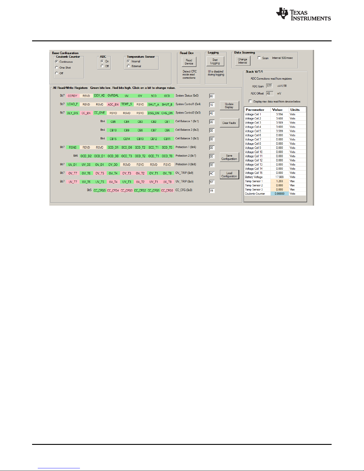
3.4.5 I2C Pro View
Figure 4 shows the I2C Pro view of the GUI. The I2C Pro view is useful to read or write several sequential
registers. If another view is displayed, it can be selected using the I2C PRO button on the left side of the
window or from the menu. The I2C Command box for each section specifies the starting register address
for the transaction.
bq76940/bq76930/bq76920 Software
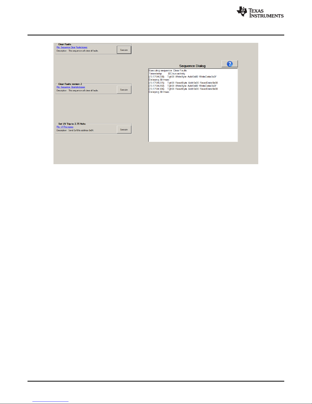
3.4.6 Sequence View
Figure 5 illustrates the Sequence view of the GUI. This is useful to send timed sequences of register
reads or writes to the device. It can be selected using the SEQUENCE button on the left side of the
window or from the menu. A sequence is run by selecting its Execute button. The results of the sequence
are shown in the Sequence Dialog section. Edit the sequence by selecting the file name under the
sequence name in the window.
SLVU924B–March 2014–Revised April 2014 bq76920 Evaluation Module User's Guide
Submit Documentation Feedback
Figure 4. I2C Pro View
9
Copyright © 2014, Texas Instruments Incorporated
Page 10
bq76940/bq76930/bq76920 Software
www.ti.com
Figure 5. Sequence View
The installation comes with 3 sequence files. The Clear Faults files contain descriptions for requirements
for a sequence file. The Set UV Trip... file shows an example of a simpler format. Sequence files are
installed to: C:\Users\<account-name>\Documents\Texas Instruments\bq76940\sequence. Sequences are
loaded from this location when the program starts. Create new sequences with a text editor and save
them with the .bqseq extension. Up to 8 sequences can be stored, move other sequences to another
directory or change the extension. The sequences Sequence_Example.bqseq, Sequence Clear
Faults.bqseq, and UVTrip.bqseq are required, do not move them from the directory.
Typical uses of a sequence might include:
• Reading and clearing faults, then enabling CHG and DSG outputs
• Setting ship mode
• Setting a balance pattern
• Any repetitive multiple-register write used in evaluation
While sequences can be executed during logging, the logging is paused while the sequence executes.
Long sequences leave gaps in the log data.
3.4.7 Typical Operation of Software
Typical operation of the software involves the following steps, much like described in quick start section:
• Connect the EVM and related equipment
• Power the EVM
• Boot the EVM
• Start the software
• Read and change registers, as desired
If the board is powered off during the evaluation process:
• Power the EVM
• Boot the EVM
• Select the Read Device button
• Read and change registers, as desired
10
bq76920 Evaluation Module User's Guide SLVU924B–March 2014–Revised April 2014
Copyright © 2014, Texas Instruments Incorporated
Submit Documentation Feedback
Page 11

www.ti.com
If the interface board is connected to a system already in operation and the software has not been exited:
• Select the Read Device button
• Read and change registers, as desired
3.4.8 Operation with Other interfaces or Hosts
The bq76940/bq76930/bq76920 software does not support other interface boards or adapters other than
the EV2300 and EV2400. The software does not operate in a multi-master environment. If operated with
another host on the line, data collisions can occur. Also be aware that the EV2400 has internal pull-up
resistors to 3.3 V, connecting to some shared busses could damage devices on that bus if the bus voltage
differs.
4 bq76920 Circuit Module Use
The bq76920 circuit module contains the bq76920 IC and related circuitry to demonstrate the features of
the IC. Surface mount FETs are provided for the high current path. A thermistor provides temperature
sensing on the board. Other components provide support for the IC and connections to the board. Basic
operation is described in the quick start guide. For details of the circuit, refer to the physical construction
section.
4.1 Cell Simulator
The EVM includes a resistive cell simulator made up of 200-Ω series resistors. The top section of the S3
switch connects the BATT+ node to the top of the resistor string. The bottom of the resistor string is
connected to BATT-. The individual cell taps are connected to the cell monitor signals by other sections of
the dip switch. When operating with a power supply all switch sections should be closed. When operating
with cells, all the dip switch sections should be open to prevent loading the cells and discharging the
battery. The cell simulator resistors are located on the bottom of the board and may become warm during
operation. The orange LED near the dip switch indicates the cell simulator has power.
bq76920 Circuit Module Use
4.2 Evaluating with Simulated Current
The quick start guide describes connection for basic operation. Providing more than recognizable current
in that configuration can require a power supply with a significant power rating. Applying a charge current
can damage some power supplies. Figure 6 shows a method to force current through the control path
without a high wattage power supply or special equipment. The load power supply should be set at a low
voltage in a constant current mode. Polarity can be reversed on the load supply to simulate a charge
current. The battery simulation supply should never be reversed.
SLVU924B–March 2014–Revised April 2014 bq76920 Evaluation Module User's Guide
Submit Documentation Feedback
11
Copyright © 2014, Texas Instruments Incorporated
Page 12

DC Power Supply
+ -
EV2300/
EV2400
I2C
SMB
DC Power Supply
+ -
(Load)
bq76920 Circuit Module Use
www.ti.com
4.3 Reducing the Cell Count
Cell count can be reduced for basic evaluation by shorting unused cells at the input terminal block. Follow
the recommendations in the datasheet for which cells to short. This works for both operation with the cell
simulator and cells, but can have some side effects in transient tests because it parallels the shorted
resistors to the cell IC where the capacitor provides a signal path to the used input. For the best
evaluation with reduced cells in a transient environment, short the VCx pins at the capacitor or VCx test
points and remove the unused input resistor. When using the cell simulator, shorting the unused cell
resistor is still required to eliminate the simulated cell voltage. Shorting the cell inputs at the terminal block
screw terminals is suggested since it should be apparent if the board is re-used for a different cell count.
(Numbered from Bottom Cell 1)
Figure 6. Simulating Current Setup
Table 3. Reducing cell count
Unused Cell
Cell 4 C4 to C3 R5 VC4 to VC3
Cell 3 C3 to C2 R6 VC3 to VC2
Short Cell Terminals Input Resistor to Remove Short AFE Inputs
12
bq76920 Evaluation Module User's Guide SLVU924B–March 2014–Revised April 2014
Copyright © 2014, Texas Instruments Incorporated
Submit Documentation Feedback
Page 13

www.ti.com
4.4 Connecting Cells
The EVM is constructed to sense the cell voltages at the cells. Separate wires are required from the
bottom of the battery stack to the C0 connection at the terminal block for sensing voltage and from the
bottom of the battery stack to the BATT- terminal to carry the load current. The AFE IC VSS is referenced
to the BATT- connection. Similarly, separate wires are required from the top of the battery stack to the top
cell input of the terminal block and from the top of the battery stack to the BATT+ terminal to carry the
load current. The top cell sense connection also powers the AFE IC. To move the sense connections from
the cells to the board, populate R1 and R2. The bottom cell simulator switch can be closed to connect C0
to BATT-.
The cell simulator provides resistors between the cell inputs. These resistors can help divide the voltage
as cells are connected. If desired, the cell simulator switches can be closed during cell connection and
opened after cell connection. The switches must be opened after connection of cells or the cells will be
discharged by the constant drain of the cell simulator. If the orange LED is on when cells are connected,
open the dip switch sections to remove the load.
Cell connection is generally considered safest from the bottom up. This minimizes the step size of the
voltage applied to the board. Recommended connection sequence for the EVM when connecting wires
individually is bottom up:
1. Connect BATT-
2. Connect cells bottom up; C0, C1, C2 ...
3. Connect BATT+
4. Open the cell simulator switches, if needed
When the top and bottom cells are connected on the board:
1. Connect BATT- (includes C0)
2. Connect cells bottom up; C1, C2, C3...
3. Connect BATT+ (includes top cell)
4. Open the cell simulator switches, if needed
When cells are mated with a connector:
1. Connect BATT- or the node which connects VSS of the AFE, if separate
2. Mate the connector
3. Connect the BATT+. if separate
4. Open the cell simulator switches, if needed
When using external balancing with P-channel MOSFETs, such as on the bq76930 and bq76940 EVMs,
the inrush current for a cell can momentarily turn on the balance FET causing the next cell input below to
rise. This can continue down the stack. Connecting C0 on the board by closing the C0 dip switch during
cell connection can reduce stress on the VC0 input of the AFE. Open the switch after cell connection for
sensing at the cell.
bq76920 Circuit Module Use
4.5 Connecting to a Host
After initial operation with the bq76940/bq76930/bq76920 software, it may be desirable to operate the
board connected to a microcontroller board. J12 could be used to connect to the microcontroller board. No
voltages should be applied to the gauge terminals. Alternately, the microcontroller is connected to the
signal test points or J8 and the ALERT test point. The interface voltage for the installed AFE IC is 2.5 V.
4.6 Gauge Circuits
The EVM contains a gauge circuit consisting of U2 and an SMBus interface connector, J14. These circuits
are reserved for future use. Only connect these circuits should only be connected to a 2.5-V output AFE
IC.
4.7 Unused Components
The EVM contains a number of component patterns which may be useful for evaluation.
SLVU924B–March 2014–Revised April 2014 bq76920 Evaluation Module User's Guide
Submit Documentation Feedback
13
Copyright © 2014, Texas Instruments Incorporated
Page 14

bq76920 Circuit Module Use
Test points are not typically populated. The patterns may be used as probe points or wires or test points
could be soldered to provide probing, if desired.
Normally the power filter R14 and C13 keeps the supply voltage for the AFE in a safe operating range. For
situations with large transients, D3 provides a clamp for the supply voltage to the AFE, if needed. The
pattern is large and it is easy to fit other component sizes. Be aware that if the system transients are large
enough that a clamp is needed at D3, the cell inputs should also be inspected for excessive voltages and
an improved filter or clamp be added there, if needed.
The ALERT line switches high and low in normal operation as status bits are asserted and cleared. A
large load is not desired since it consumes power. If it is useful to slow the transition, the pattern C10 is
available. C10 should not be large in order to avoid current and slowing the edge to where the bq76920
would see the ALERT high as an input and set the OVRD_ALERT condition.
When the charge FET turns on with a large charger voltage present, a large voltage could be impressed
on the gate of the charge FET. With the voltages typically used on the bq76920EVM, this should not be
high enough to damage the charge FET. If special circumstances require, the D5 pattern is available for a
clamp diode.
D6 is a flyback diode to prevent PACK- from rising significantly above PACK+. The D7 pattern provides a
place to mount a higher current diode or other transient suppression component.
HS1 is a position to mount a suitable heatsink, if needed. Other heatsink options may be available in the
evaluation environment.
www.ti.com
14
bq76920 Evaluation Module User's Guide SLVU924B–March 2014–Revised April 2014
Copyright © 2014, Texas Instruments Incorporated
Submit Documentation Feedback
Page 15

www.ti.com
5 bq76920EVM Circuit Module Physical Construction
This section contains the PCB layout, bill of materials, and schematic of the bq76920EVM circuit module.
The bq76920EVM consists of one circuit module assembly, PWR523.
5.1 Board Layout
The bq76920EVM circuit module is a 4.0-inch × 4.805-inch 4-layer circuit card assembly. It is designed for
easy assembly with cell connections on the left side to a terminal block and high current terminals through
banana jacks. Control connections are on the left top. Pack terminals are on the right side using banana
jacks. Wide trace areas are used reducing voltage drops on the high current paths. The EVM layout and
construction allows easy understanding of the connections and access to the test points for evaluation, but
the connector area and programming features result in a large board.
See additional information in the configuration and operation sections of this document. Figure 7 to
Figure 14 show the board layout.
bq76920EVM Circuit Module Physical Construction
SLVU924B–March 2014–Revised April 2014 bq76920 Evaluation Module User's Guide
Submit Documentation Feedback
Figure 7. Top Silk Screen
15
Copyright © 2014, Texas Instruments Incorporated
Page 16

bq76920EVM Circuit Module Physical Construction
www.ti.com
16
bq76920 Evaluation Module User's Guide SLVU924B–March 2014–Revised April 2014
Figure 8. Top Assembly
Copyright © 2014, Texas Instruments Incorporated
Submit Documentation Feedback
Page 17

www.ti.com
bq76920EVM Circuit Module Physical Construction
SLVU924B–March 2014–Revised April 2014 bq76920 Evaluation Module User's Guide
Submit Documentation Feedback
Figure 9. Top Layer
17
Copyright © 2014, Texas Instruments Incorporated
Page 18

bq76920EVM Circuit Module Physical Construction
www.ti.com
18
bq76920 Evaluation Module User's Guide SLVU924B–March 2014–Revised April 2014
Figure 10. Layer 2
Copyright © 2014, Texas Instruments Incorporated
Submit Documentation Feedback
Page 19

www.ti.com
bq76920EVM Circuit Module Physical Construction
SLVU924B–March 2014–Revised April 2014 bq76920 Evaluation Module User's Guide
Submit Documentation Feedback
Figure 11. Layer 3
19
Copyright © 2014, Texas Instruments Incorporated
Page 20

bq76920EVM Circuit Module Physical Construction
www.ti.com
20
bq76920 Evaluation Module User's Guide SLVU924B–March 2014–Revised April 2014
Figure 12. Bottom Layer
Copyright © 2014, Texas Instruments Incorporated
Submit Documentation Feedback
Page 21

www.ti.com
bq76920EVM Circuit Module Physical Construction
SLVU924B–March 2014–Revised April 2014 bq76920 Evaluation Module User's Guide
Submit Documentation Feedback
Figure 13. Bottom Silk Screen
21
Copyright © 2014, Texas Instruments Incorporated
Page 22

bq76920EVM Circuit Module Physical Construction
www.ti.com
22
bq76920 Evaluation Module User's Guide SLVU924B–March 2014–Revised April 2014
Figure 14. Bottom Assembly
Copyright © 2014, Texas Instruments Incorporated
Submit Documentation Feedback
Page 23

www.ti.com
bq76920EVM Circuit Module Physical Construction
5.2 Bill of Materials
The bill of materials for the circuit module is shown in Table 4. Substitute parts may be used in the manufacturing of the assembly.
Table 4. bq76920 Circuit Module Bill of Materials
Designator Qty Value Description PackageReference Part Number MFG Alternate Alternate
Part Number MFG
PCB1 1 Printed Circuit Board PWR523 Any - C1, C2, C3, C4, C5, C6, C14 7 1uF CAP, CERM, 1uF, 16V, +/-10%, X7R, 0805 0805 GRM21BR71C105KA01L MuRata
C7, C8, C9, C11, C12, C17, C18, 10 0.1uF CAP, CERM, 0.1uF, 50V, +/-10%, X7R, 0603 0603 GCM188R71H104KA57B MuRata
C21, C22, C23
C13 1 2.2uF CAP, CERM, 2.2uF, 50V, +/-10%, X5R, 1206 1206 GRM31CR61H225KA88L MuRata
C15 1 4700pF CAP,CERM, 4700pF, 50V, +/-10%, X7R, 0805 0805 08055C472KAT2A AVX
C16 1 4.7uF CAP, CERM, 4.7uF, 10V, +/-10%, X7R, 0805 0805 GRM21BR71A475KA73L MuRata
C20 1 3300pF CAP,CERM, 3300pF, 25V, +/-10%, X7R, 0603 0603 GRM188R71E332KA01D MuRata
D1 1 28V Diode, TVS, Uni, 28V, 1500W, SMC SMC SMCJ28A Fairchild Semiconductor
D2, D4, D12 3 1.25V Diode, Ultrafast, 100V, 0.15A, SOD-123 SOD-123 1N4148W-7-F Diodes Inc.
D6 1 600V Diode, Ultrafast, 600V, 3A, SMC SMC MURS360T3G ON Semiconductor
D8, D9, D10, D11, D19, D20 6 5.6V Diode, Zener, 5.6V, 200mW, SOD-323 SOD-323 MMSZ5232BS-7-F Diodes Inc.
D13 1 16V Diode, Zener, 16V, 500mW, SOD-123 SOD-123 MMSZ5246B-7-F Diodes Inc.
D14, D15, D16, D17, D18 5 Green LED, Green, SMD 1.6x0.8x0.8mm LTST-C190GKT Lite-On
D21 1 Orange LED, Orange, SMD 1.6x0.8x0.8mm LTST-C190KFKT Lite-On
H1, H2, H5, H6 4 Machine Screw, Round, #4-40 x 1/4, Nylon, Philips panhead Screw NY PMS 440 0025 PH B&FFastener Supply - H3, H4, H7, H8 4 Standoff, Hex, 0.5"L #4-40 Nylon Standoff 1902C Keystone - J1 1 Receptacle, 3.5mm 6x1, R/A, TH Header, 6x1 R/A 395021006 Molex
J2, J3, J6, J7 4 Standard Banana Jack, Uninsulated, 15A Banana Jack 108-0740-001 Emerson Network Power
J4, J5, J9, J10 4 Header, 100mil, 2x1, Tin plated, TH Header, 2 PIN, 100mil, Tin PEC02SAAN Sullins Connector Solutions
J8, J14 2 Header, 100mil, 4x1, R/A, TH 4x1 R/A Header 22-05-3041 Molex
J12 1 Header, 100mil, 5x2, Tin plated, TH Header,5x2, 100mil, Tin PEC05DAAN Sullins Connector Solutions
J13 1 Header, 100mil, 3x1, Tin plated, TH Header,3 PIN, 100mil, Tin PEC03SAAN Sullins Connector Solutions
P1 1 CONN TERM BLOCK 3.5MM 6POS R/A Term Block Plug 39500-0006 Molex - Q1, Q2 2 30V MOSFET, N-CH, 30V, 100A, SON 5x6mm SON 5x6mm CSD17501Q5A Texas Instruments None
Q3, Q4 2 -50V MOSFET, P-CH, -50V, -0.13A, SOT-323 SOT-323 BSS84W-7-F Diodes Inc. None
Q5, Q6, Q8 3 50V MOSFET, N-CH, 50V, 0.22A, SOT-23 SOT-23 BSS138 Fairchild Semiconductor None
Q7 1 0.25V Transistor, PNP, 40V, 0.2A, SOT-23 SOT-23 MMBT3906 Fairchild Semiconductor None None
Q9 1 0.5V Transistor, NPN, 80V, 1A, SOT-89 SOT-89 BCX5616TA Diodes Inc.
R3, R21, R23, R51, R55 5 10.0k RES, 10.0k ohm, 1%, 0.125W, 0805 0805 CRCW080510K0FKEA Vishay-Dale
R4, R5, R6, R7, R8, R9 6 100 RES, 100 ohm, 1%, 0.25W, 1206 1206 CRCW1206100RFKEA Vishay-Dale
R10, R12, R14, R24, R25, R26, R27, 15 100 RES, 100 ohm, 1%, 0.125W, 0805 0805 CRCW0805100RFKEA Vishay-Dale
R31, R32, R36, R37, R57, R58, R61,
R62
R11 1 0.001 RES, 0.001 ohm, 1%, 2W, 4527 4527 WSR21L000FEA Vishay-Dale
R13 1 499k RES, 499k ohm, 1%, 0.125W, 0805 0805 CRCW0805499KFKEA Vishay-Dale
R15, R18, R19, R47, R54, R59, R60 7 1.00Meg RES, 1.00Meg ohm, 1%, 0.125W, 0805 0805 CRCW08051M00FKEA Vishay-Dale
23
SLVU924B– March 2014–Revised April 2014 bq76920 Evaluation Module User's Guide
Submit Documentation Feedback
Copyright © 2014, Texas Instruments Incorporated
Page 24

bq76920EVM Circuit Module Physical Construction
www.ti.com
Table 4. bq76920 Circuit Module Bill of Materials (continued)
Designator Qty Value Description PackageReference Part Number MFG Alternate Alternate
Part Number MFG
R16, R30 2 0 RES, 0 ohm, 5%, 0.125W, 0805 0805 CRCW08050000Z0EA Vishay-Dale
R17 1 1.00k RES, 1.00k ohm, 1%, 0.125W, 0805 0805 CRCW08051K00FKEA Vishay-Dale
R20 1 10.0k Thermistor NTC, 10.0k ohm, 1%, Disc, 5x8.4 mm Disc, 5x8.4 mm 103AT-2 SEMITEC Corporation
ohm
R22 1 3.01k RES, 3.01k ohm, 1%, 0.125W, 0805 0805 CRCW08053K01FKEA Vishay-Dale
R38 1 300k RES, 300k ohm, 0.1%, 0.1W, 0603 0603 RG1608P-304-B-T5 Susumu Co Ltd
R39, R43 2 13.7k RES, 13.7k ohm, 0.1%, 0.1W, 0603 0603 RG1608P-1372-B-T5 Susumu Co Ltd
R44, R45, R50, R52 4 100k RES, 100k ohm, 1%, 0.125W, 0805 0805 CRCW0805100KFKEA Vishay-Dale
R46 1 0 RES, 0 ohm, 5%, 0.25W, 1206 1206 CRCW12060000Z0EA Vishay-Dale
R48 1 1.0k RES, 1.0k ohm, 5%, 1W, 2512 2512 ERJ-1TYJ102U Panasonic
R49 1 196k RES, 196k ohm, 1%, 0.125W, 0805 0805 CRCW0805196KFKEA Vishay-Dale
R53 1 49.9k RES, 49.9k ohm, 1%, 0.125W, 0805 0805 CRCW080549K9FKEA Vishay-Dale
R63 1 221k RES, 221k ohm, 1%, 0.125W, 0805 0805 CRCW0805221KFKEA Vishay-Dale
R64, R65 2 1.00k RES, 1.00k ohm, 1%, 0.25W, 1206 1206 CRCW12061K00FKEA Vishay-Dale
R66, R67, R68, R69, R70 5 200 RES, 200 ohm, 1%, 0.125W, 0805 0805 CRCW0805200RFKEA Vishay-Dale
S1, S2 2 Switch, Tactile, SPST-NO, 0.05A, 12V, SMT SW,SPST 6x6 mm 4-1437565-1 TE Connectivity
S3 1 Switch, SPST 7Pos, Rocker, TH 9.65X8X19.8mm 76SB07ST Grayhill
SH-J4, SH-J5, SH-J9, SH-J10, SH- 9 1x2 Shunt, 100mil, Gold plated, Black Shunt 969102-0000-DA 3M SNT-100-BK-G Samtec
J12-3, SH-J12-5, SH-J12-7, SH-J129, SH-J13-3
TP3, TP4, TP5, TP6 4 Black Test Point, TH, Multipurpose, Black Keystone5011 5011 Keystone
U1 1 µC-Controlled AFE Family for 5/10/15-Series Cell Lithium-Ion PW0020A BQ7692000PW Texas Instruments None
and Phosphate Battery Pack Applications, PW0020A
U2 1 CEDV Fuel Gauge and Battery Management Controller DBT0030A BQ78350DBT Texas Instruments None
Companion to the bq769x0 AFE, DBT0030A
W1 1 Cable assembly, 4 pin Assembly CBL002 Texas Instruments - C10 0 470pF CAP, CERM, 470pF, 50V, +/-10%, X7R, 0805 0805 08055C471KAT2A AVX
C19 0 3300pF CAP,CERM, 3300pF, 25V, +/-10%, X7R, 0603 0603 GRM188R71E332KA01D MuRata
D3 0 30V Diode, TVS, Uni, 30V, 600W, SMB SMB SMBJ30A-13-F Diodes Inc.
D5 0 16V Diode, Zener, 16V, 500mW, SOD-123 SOD-123 MMSZ5246B-7-F Diodes Inc.
D7 0 600V Diode, Ultrafast, 600V, 8A, TH TO-220AC MUR860G ON Semiconductor
FID1, FID2, FID3 0 Fiducial mark. There is nothing to buy or mount. Fiducial N/A N/A
HS1 0 Heatsink, DDPAK/TO-263, SMT Heatsink, DDPAk 573300D00010G Aavid
J11 0 Header, TH, 100mil, 7x1, Gold plated, 230 mil above 7x1 Header TSW-107-07-G-S Samtec
insulator
J15 0 Header, TH, 100mil, 6x1, Gold plated, 230 mil above TSW-106-07-G-S TSW-106-07-G-S Samtec, Inc.
insulator
R1, R2 0 0 RES, 0 ohm, 5%, 0.125W, 0805 0805 CRCW08050000Z0EA Vishay-Dale
R28, R29, R40, R41, R56 0 1.00k RES, 1.00k ohm, 1%, 0.125W, 0805 0805 CRCW08051K00FKEA Vishay-Dale
R33 0 300k RES, 300k ohm, 0.1%, 0.1W, 0603 0603 RG1608P-304-B-T5 Susumu Co Ltd
R34, R35, R42 0 1.00Meg RES, 1.00Meg ohm, 1%, 0.125W, 0805 0805 CRCW08051M00FKEA Vishay-Dale
TP1 0 Black Test Point, TH, Multipurpose, Black Keystone5011 5011 Keystone
24
bq76920 Evaluation Module User's Guide SLVU924B– March 2014–Revised April 2014
Submit Documentation Feedback
Copyright © 2014, Texas Instruments Incorporated
Page 25

www.ti.com
bq76920EVM Circuit Module Physical Construction
Table 4. bq76920 Circuit Module Bill of Materials (continued)
Designator Qty Value Description PackageReference Part Number MFG Alternate Alternate
Part Number MFG
TP2, TP29 0 Red Test Point, TH, Multipurpose, Red Keystone5010 5010 Keystone
TP7, TP8, TP9, TP10, TP11, TP12, 0 White Test Point, TH, Multipurpose, White Keystone5012 5012 Keystone
TP13, TP14, TP15, TP18, TP20,
TP21, TP22, TP24, TP25, TP26,
TP27, TP28, TP33, TP34, TP35,
TP37
25
SLVU924B– March 2014–Revised April 2014 bq76920 Evaluation Module User's Guide
Submit Documentation Feedback
Copyright © 2014, Texas Instruments Incorporated
Page 26

DSG
1
CHG
2
VSS
3
SDA
4
SCL
5
TS1
6
CAP1
7
REGOUT
8
REGSRC
9
BAT
10
NC
11
VC5
12
VC4
13
VC3
14
VC2
15
VC1
16
VC0
17
SRP
18
SRN
19
ALERT
20
U1
BQ7692000PW
1µF
C1
100
R5
5
4
1
2
3
6
J1
395021006
1µF
C2
1µF
C3
1µF
C4
1µF
C5
1µF
C6
100
R4
100
R6
100
R7
100
R8
100
R9
4.7µF
C16
2.2µF
C13
1.25V
D2
J2
108-0740-001
0.001
R11
100
R10
100
R12
0.1µF
C8
0.1µF
C9
0.1µF
C7
TP10
DNP
TP12
DNP
TP15
DNP
TP8
DNP
TP21
DNP
TP17
TP20
DNP
TP23
DNP
30V
D3
SMBJ30A-13-F
DNP
100
R14
100
R24
100
R25
499k
R13
4
1
2
3
J8
22-05-3041
10.0k
R23
10.0k
R21
TP19
1
2
J5
PEC02SAAN
1
2
J4
PEC02SAAN
J3
108-0740-001
600V
D7
MUR860G
DNP
4
7,8
1,2,3
5,6,
30V
Q1
CSD17501Q5A
4
7,8
1,2,3
5,6,
30V
Q2
CSD17501Q5A
600V
D6
MURS360T3G
1.00Meg
R19
1.00Meg
R15
GND GND
GND
GND
GND
J6
108-0740-001
J7
108-0740-001
0.1µF
C11
0.1µF
C12
0.1µF
C17
0.1µF
C18
1µF
C14
0
R16
1.00k
R17
1.00Meg
R18
-50V
Q3
BSS84W-7-F
16V
D5
MMSZ5246B-7-F
DNP
1.25V
D4
GND
10.0k Ω
t°
R20
4700pF
C15
GND
GND
TP9
DNP
TP11
DNP
TP13
DNP
TP14
DNP
TP7
DNP
TP18
DNP
TP24
DNP
TP27
DNP
TP26
DNP
TP25
DNP
TP22
DNP
NT1
Net-Tie
BATT– GND
BATT-
E2 E4
E3
E1
BATT–
123
4
S1
4-1437565-1
3.01k
R22
5.6V
D8
5.6V
D9
HS1
573300D00010G
DNP
TP3 TP4 TP5 TP6
TP1
DNP
TP2
DNP
TP29
DNP
TP28
DNP
GND
0
R2
DNP
0
R1
DNP
C5
C4
C3
C2
C1
C0
BATR
SCL pull up
SDA pull up
BATT+
10.0k
R3
–
Input voltage 0 - 25 V
0 - 15 A
+
–
Output voltage 0 - 25 V
0 - 15 A
+
28V
D1
SMCJ28A
100
R26
100
R27
ALERT
470pF
C10
DNP
DSG
CHG
CAP1 SDA
SCL
REGOUT
C1
C0
C1
C2
C3
C4
C5
BATT+
BATT+
PFD
PACK–
I C
2
BOOT
TP16
bq76920EVM Circuit Module Physical Construction
www.ti.com
Figure 15 through Figure 17 illustrate the schematics.
Figure 15. Schematic Diagram AFE
26
bq76920 Evaluation Module User's Guide SLVU924B– March 2014–Revised April 2014
Submit Documentation Feedback
Copyright © 2014, Texas Instruments Incorporated
Page 27

NC
1
ALERT
2
SDA
3
SCL
4
PRECHG
5
VAUX
6
BAT
7
PRES
8
KEYIN
9
SAFE
10
SMBD
11
VEN
12
SMBC
13
DISP
14
PWRM
15
LED1
16
LED2
17
LED3
18
LED4
19
LED5
20
VSS
21
VSS
22
VSS
23
MRST
24
VSS
25
VCC
26
RBI
27
NC
28
ADREN
29
SMBA
30
U2
BQ78350DBT
50V
Q6
BSS138
1.00Meg
R54
1.0k
R48
100
R58
100
R61
100
R57
100
R62
4
1
2
3
J14
22-05-3041
GND
BATT–
E7 E8
BATT–
1.00Meg
R60
1.00Meg
R59
GND
GND
123
4
S2
4-1437565-1
1
2
J10
PEC02SAAN
100
R31
100
R36
100
R32
100
R37
BATT-
1
2
J9
PEC02SAAN
50V
Q8
BSS138
MMBT3906
Q7
10.0k
R51
1.25V
D12
GND
0.1µF
C22
10.0k
R55
TP34
DNP
TP35
DNP
TP32
196k
R49
49.9k
R53
100k
R52
Green
D17
Green
D16
Green
D15
Green
D14
Green
D18
221k
R63
GND
GND
GND
GND
GND
0.1µF
C21
1
2
3
J13
PEC03SAAN
GND
1.00Meg
R34
DNP
1.00Meg
R35
DNP
GND
ALT
16/17
Addr select
GG_PWR
GG_SCL
GG_SDA
GG_ALERT
GG_/KEYIN
GG_/PRES
SMBA
16V
D13
MMSZ5246B-7-F
5.6V
D11
5.6V
D10
5.6V
D20
5.6V
D19
TP37
TP33
DNP
/KEYIN
/PRES
1 2
3 4
5 6
7 8
9 10
J12
PEC05DAAN
GND
GG_PWR
0
R30
TP36
AFE-GG
BCX5616TA
1
3
2,4
Q9
SMB
0.1µF
C23
GND
DISPLAY
100k
R50E6E5
SCL
SDA
REGOUT
ALERT
C5
CAP1
PFD PACK–
1.00k
R40
DNP
1.00k
R41
DNP
300k
25 ppm/C
R38
13.7k
25 ppm/C
R43
50V
Q5
BSS138
-50V
Q4
BSS84W-7-F
100k
R45
TP30 TP31
100k
R44
5
4
1
2
3
6
7
J11
TSW-107-07-G-S
DNP
13.7k
25 ppm/C
R39
GND GND GND
3300pF
C20
3300pF
C19
DNP
GND
300k
25 ppm/C
R33
DNP
1.00k
R28
DNP
1.00k
R29
DNP
CHG
DSG
1.00k
R56
DNP
EDSG
ECHG
EPM
EVEN
EVAUX
0
R46
1.00Meg
R42
DNP
1.00Meg
R47
EPCHG
DNP
www.ti.com
bq76920EVM Circuit Module Physical Construction
Figure 16. Schematic Diagram Gauge
27
SLVU924B– March 2014–Revised April 2014 bq76920 Evaluation Module User's Guide
Submit Documentation Feedback
Copyright © 2014, Texas Instruments Incorporated
Page 28

200
R66
200
R67
200
R68
200
R69
200
R70
1.00k
R65
1
2
3
4
5
6
13
14
7
12
10
11
8
9
S3
76SB07ST
Orange
D21
GND
5
4
1
2
3
6
J15
DNP
BATT–
Test points
BATT+
C5
C4
C3
C2
C1
C0
1.00k
R64
bq76920EVM Circuit Module Physical Construction
www.ti.com
Figure 17. Schematic Diagram Cell Simulator
28
bq76920 Evaluation Module User's Guide SLVU924B– March 2014–Revised April 2014
Submit Documentation Feedback
Copyright © 2014, Texas Instruments Incorporated
Page 29

www.ti.com
Related Documents From Texas Instruments
6 Related Documents From Texas Instruments
Document Literature
Number
bq76920, bq76930, bq76940 μC-Controlled AFE Family for 5-, 10-, and 15-Series SLUSBK2
Cell Lithium-Ion and Phosphate Battery Pack Applications Data Sheet
Revision History
Changes from Original (March 2014) to A Revision ....................................................................................................... Page
• Changed software display image........................................................................................................ 6
• Changed registers view image........................................................................................................... 8
NOTE: Page numbers for previous revisions may differ from page numbers in the current version.
Revision History
Changes from A Revision (April 2014) to B Revision .................................................................................................... Page
• Changed software title to bq76940/bq76930/bq76920 Evaluation Software in step one of the Quick Start section and
globally throughout document. .......................................................................................................... 4
• Added clarification about device identifiers in menus or windows in the bq76940/bq76930/bq76920 Software section.... 5
• Changed path name to ...'\bq76940' in second paragraph of Interface Adapter section......................................... 6
• Added sentence about how to start the software in the Software Operation section............................................. 6
• Changed Evaluation Software Display image. ........................................................................................ 6
• Added Sequence_Example.bqseq to paragraph below Sequence View image................................................. 10
• Changed content in the BOM in rows containing U1 and U2 in the Designator column. ...................................... 23
NOTE: Page numbers for previous revisions may differ from page numbers in the current version.
SLVU924B–March 2014–Revised April 2014 Revision History
Submit Documentation Feedback
29
Copyright © 2014, Texas Instruments Incorporated
Page 30

ADDITIONAL TERMS AND CONDITIONS, WARNINGS, RESTRICTIONS, AND DISCLAIMERS FOR
EVALUATION MODULES
Texas Instruments Incorporated (TI) markets, sells, and loans all evaluation boards, kits, and/or modules (EVMs) pursuant to, and user
expressly acknowledges, represents, and agrees, and takes sole responsibility and risk with respect to, the following:
1. User agrees and acknowledges that EVMs are intended to be handled and used for feasibility evaluation only in laboratory and/or
development environments. Notwithstanding the foregoing, in certain instances, TI makes certain EVMs available to users that do not
handle and use EVMs solely for feasibility evaluation only in laboratory and/or development environments, but may use EVMs in a
hobbyist environment. All EVMs made available to hobbyist users are FCC certified, as applicable. Hobbyist users acknowledge, agree,
and shall comply with all applicable terms, conditions, warnings, and restrictions in this document and are subject to the disclaimer and
indemnity provisions included in this document.
2. Unless otherwise indicated, EVMs are not finished products and not intended for consumer use. EVMs are intended solely for use by
technically qualified electronics experts who are familiar with the dangers and application risks associated with handling electrical
mechanical components, systems, and subsystems.
3. User agrees that EVMs shall not be used as, or incorporated into, all or any part of a finished product.
4. User agrees and acknowledges that certain EVMs may not be designed or manufactured by TI.
5. User must read the user's guide and all other documentation accompanying EVMs, including without limitation any warning or
restriction notices, prior to handling and/or using EVMs. Such notices contain important safety information related to, for example,
temperatures and voltages. For additional information on TI's environmental and/or safety programs, please visit www.ti.com/esh or
contact TI.
6. User assumes all responsibility, obligation, and any corresponding liability for proper and safe handling and use of EVMs.
7. Should any EVM not meet the specifications indicated in the user’s guide or other documentation accompanying such EVM, the EVM
may be returned to TI within 30 days from the date of delivery for a full refund. THE FOREGOING LIMITED WARRANTY IS THE
EXCLUSIVE WARRANTY MADE BY TI TO USER AND IS IN LIEU OF ALL OTHER WARRANTIES, EXPRESSED, IMPLIED, OR
STATUTORY, INCLUDING ANY WARRANTY OF MERCHANTABILITY OR FITNESS FOR ANY PARTICULAR PURPOSE. TI SHALL
NOT BE LIABLE TO USER FOR ANY INDIRECT, SPECIAL, INCIDENTAL, OR CONSEQUENTIAL DAMAGES RELATED TO THE
HANDLING OR USE OF ANY EVM.
8. No license is granted under any patent right or other intellectual property right of TI covering or relating to any machine, process, or
combination in which EVMs might be or are used. TI currently deals with a variety of customers, and therefore TI’s arrangement with
the user is not exclusive. TI assumes no liability for applications assistance, customer product design, software performance, or
infringement of patents or services with respect to the handling or use of EVMs.
9. User assumes sole responsibility to determine whether EVMs may be subject to any applicable federal, state, or local laws and
regulatory requirements (including but not limited to U.S. Food and Drug Administration regulations, if applicable) related to its handling
and use of EVMs and, if applicable, compliance in all respects with such laws and regulations.
10. User has sole responsibility to ensure the safety of any activities to be conducted by it and its employees, affiliates, contractors or
designees, with respect to handling and using EVMs. Further, user is responsible to ensure that any interfaces (electronic and/or
mechanical) between EVMs and any human body are designed with suitable isolation and means to safely limit accessible leakage
currents to minimize the risk of electrical shock hazard.
11. User shall employ reasonable safeguards to ensure that user’s use of EVMs will not result in any property damage, injury or death,
even if EVMs should fail to perform as described or expected.
12. User shall be solely responsible for proper disposal and recycling of EVMs consistent with all applicable federal, state, and local
requirements.
Certain Instructions. User shall operate EVMs within TI’s recommended specifications and environmental considerations per the user’s
guide, accompanying documentation, and any other applicable requirements. Exceeding the specified ratings (including but not limited to
input and output voltage, current, power, and environmental ranges) for EVMs may cause property damage, personal injury or death. If
there are questions concerning these ratings, user should contact a TI field representative prior to connecting interface electronics including
input power and intended loads. Any loads applied outside of the specified output range may result in unintended and/or inaccurate
operation and/or possible permanent damage to the EVM and/or interface electronics. Please consult the applicable EVM user's guide prior
to connecting any load to the EVM output. If there is uncertainty as to the load specification, please contact a TI field representative. During
normal operation, some circuit components may have case temperatures greater than 60°C as long as the input and output are maintained
at a normal ambient operating temperature. These components include but are not limited to linear regulators, switching transistors, pass
transistors, and current sense resistors which can be identified using EVMs’ schematics located in the applicable EVM user's guide. When
placing measurement probes near EVMs during normal operation, please be aware that EVMs may become very warm. As with all
electronic evaluation tools, only qualified personnel knowledgeable in electronic measurement and diagnostics normally found in
development environments should use EVMs.
Agreement to Defend, Indemnify and Hold Harmless. User agrees to defend, indemnify, and hold TI, its directors, officers, employees,
agents, representatives, affiliates, licensors and their representatives harmless from and against any and all claims, damages, losses,
expenses, costs and liabilities (collectively, "Claims") arising out of, or in connection with, any handling and/or use of EVMs. User’s
indemnity shall apply whether Claims arise under law of tort or contract or any other legal theory, and even if EVMs fail to perform as
described or expected.
Safety-Critical or Life-Critical Applications. If user intends to use EVMs in evaluations of safety critical applications (such as life support),
and a failure of a TI product considered for purchase by user for use in user’s product would reasonably be expected to cause severe
personal injury or death such as devices which are classified as FDA Class III or similar classification, then user must specifically notify TI
of such intent and enter into a separate Assurance and Indemnity Agreement.
Page 31

RADIO FREQUENCY REGULATORY COMPLIANCE INFORMATION FOR EVALUATION MODULES
Texas Instruments Incorporated (TI) evaluation boards, kits, and/or modules (EVMs) and/or accompanying hardware that is marketed, sold,
or loaned to users may or may not be subject to radio frequency regulations in specific countries.
General Statement for EVMs Not Including a Radio
For EVMs not including a radio and not subject to the U.S. Federal Communications Commission (FCC) or Industry Canada (IC)
regulations, TI intends EVMs to be used only for engineering development, demonstration, or evaluation purposes. EVMs are not finished
products typically fit for general consumer use. EVMs may nonetheless generate, use, or radiate radio frequency energy, but have not been
tested for compliance with the limits of computing devices pursuant to part 15 of FCC or the ICES-003 rules. Operation of such EVMs may
cause interference with radio communications, in which case the user at his own expense will be required to take whatever measures may
be required to correct this interference.
General Statement for EVMs including a radio
User Power/Frequency Use Obligations: For EVMs including a radio, the radio included in such EVMs is intended for development and/or
professional use only in legally allocated frequency and power limits. Any use of radio frequencies and/or power availability in such EVMs
and their development application(s) must comply with local laws governing radio spectrum allocation and power limits for such EVMs. It is
the user’s sole responsibility to only operate this radio in legally acceptable frequency space and within legally mandated power limitations.
Any exceptions to this are strictly prohibited and unauthorized by TI unless user has obtained appropriate experimental and/or development
licenses from local regulatory authorities, which is the sole responsibility of the user, including its acceptable authorization.
U.S. Federal Communications Commission Compliance
For EVMs Annotated as FCC – FEDERAL COMMUNICATIONS COMMISSION Part 15 Compliant
Caution
This device complies with part 15 of the FCC Rules. Operation is subject to the following two conditions: (1) This device may not cause
harmful interference, and (2) this device must accept any interference received, including interference that may cause undesired operation.
Changes or modifications could void the user's authority to operate the equipment.
FCC Interference Statement for Class A EVM devices
This equipment has been tested and found to comply with the limits for a Class A digital device, pursuant to part 15 of the FCC Rules.
These limits are designed to provide reasonable protection against harmful interference when the equipment is operated in a commercial
environment. This equipment generates, uses, and can radiate radio frequency energy and, if not installed and used in accordance with the
instruction manual, may cause harmful interference to radio communications. Operation of this equipment in a residential area is likely to
cause harmful interference in which case the user will be required to correct the interference at its own expense.
FCC Interference Statement for Class B EVM devices
This equipment has been tested and found to comply with the limits for a Class B digital device, pursuant to part 15 of the FCC Rules.
These limits are designed to provide reasonable protection against harmful interference in a residential installation. This equipment
generates, uses and can radiate radio frequency energy and, if not installed and used in accordance with the instructions, may cause
harmful interference to radio communications. However, there is no guarantee that interference will not occur in a particular installation. If
this equipment does cause harmful interference to radio or television reception, which can be determined by turning the equipment off and
on, the user is encouraged to try to correct the interference by one or more of the following measures:
• Reorient or relocate the receiving antenna.
• Increase the separation between the equipment and receiver.
• Connect the equipment into an outlet on a circuit different from that to which the receiver is connected.
• Consult the dealer or an experienced radio/TV technician for help.
Industry Canada Compliance (English)
For EVMs Annotated as IC – INDUSTRY CANADA Compliant:
This Class A or B digital apparatus complies with Canadian ICES-003.
Changes or modifications not expressly approved by the party responsible for compliance could void the user’s authority to operate the
equipment.
Concerning EVMs Including Radio Transmitters
This device complies with Industry Canada licence-exempt RSS standard(s). Operation is subject to the following two conditions: (1) this
device may not cause interference, and (2) this device must accept any interference, including interference that may cause undesired
operation of the device.
Concerning EVMs Including Detachable Antennas
Under Industry Canada regulations, this radio transmitter may only operate using an antenna of a type and maximum (or lesser) gain
approved for the transmitter by Industry Canada. To reduce potential radio interference to other users, the antenna type and its gain should
be so chosen that the equivalent isotropically radiated power (e.i.r.p.) is not more than that necessary for successful communication.
This radio transmitter has been approved by Industry Canada to operate with the antenna types listed in the user guide with the maximum
permissible gain and required antenna impedance for each antenna type indicated. Antenna types not included in this list, having a gain
greater than the maximum gain indicated for that type, are strictly prohibited for use with this device.
Page 32

Canada Industry Canada Compliance (French)
Cet appareil numérique de la classe A ou B est conforme à la norme NMB-003 du Canada
Les changements ou les modifications pas expressément approuvés par la partie responsable de la conformité ont pu vider l’autorité de
l'utilisateur pour actionner l'équipement.
Concernant les EVMs avec appareils radio
Le présent appareil est conforme aux CNR d'Industrie Canada applicables aux appareils radio exempts de licence. L'exploitation est
autorisée aux deux conditions suivantes : (1) l'appareil ne doit pas produire de brouillage, et (2) l'utilisateur de l'appareil doit accepter tout
brouillage radioélectrique subi, même si le brouillage est susceptible d'en compromettre le fonctionnement.
Concernant les EVMs avec antennes détachables
Conformément à la réglementation d'Industrie Canada, le présent émetteur radio peut fonctionner avec une antenne d'un type et d'un gain
maximal (ou inférieur) approuvé pour l'émetteur par Industrie Canada. Dans le but de réduire les risques de brouillage radioélectrique à
l'intention des autres utilisateurs, il faut choisir le type d'antenne et son gain de sorte que la puissance isotrope rayonnée équivalente
(p.i.r.e.) ne dépasse pas l'intensité nécessaire à l'établissement d'une communication satisfaisante.
Le présent émetteur radio a été approuvé par Industrie Canada pour fonctionner avec les types d'antenne énumérés dans le manuel
d’usage et ayant un gain admissible maximal et l'impédance requise pour chaque type d'antenne. Les types d'antenne non inclus dans
cette liste, ou dont le gain est supérieur au gain maximal indiqué, sont strictement interdits pour l'exploitation de l'émetteur.
Mailing Address: Texas Instruments, Post Office Box 655303, Dallas, Texas 75265
Copyright © 2014, Texas Instruments Incorporated
spacer
Important Notice for Users of EVMs Considered “Radio Frequency Products” in Japan
EVMs entering Japan are NOT certified by TI as conforming to Technical Regulations of Radio Law of Japan.
If user uses EVMs in Japan, user is required by Radio Law of Japan to follow the instructions below with respect to EVMs:
1. Use EVMs in a shielded room or any other test facility as defined in the notification #173 issued by Ministry of Internal Affairs and
Communications on March 28, 2006, based on Sub-section 1.1 of Article 6 of the Ministry’s Rule for Enforcement of Radio Law of
Japan,
2. Use EVMs only after user obtains the license of Test Radio Station as provided in Radio Law of Japan with respect to EVMs, or
3. Use of EVMs only after user obtains the Technical Regulations Conformity Certification as provided in Radio Law of Japan with respect
to EVMs. Also, do not transfer EVMs, unless user gives the same notice above to the transferee. Please note that if user does not
follow the instructions above, user will be subject to penalties of Radio Law of Japan.
http://www.tij.co.jp
【無線電波を送信する製品の開発キットをお使いになる際の注意事項】 本開発キットは技術基準適合証明を受けておりません。 本製品の
ご使用に際しては、電波法遵守のため、以下のいずれかの措置を取っていただく必要がありますのでご注意ください。
1. 電波法施行規則第6条第1項第1号に基づく平成18年3月28日総務省告示第173号で定められた電波暗室等の試験設備でご使用いただく。
2. 実験局の免許を取得後ご使用いただく。
3. 技術基準適合証明を取得後ご使用いただく。。
なお、本製品は、上記の「ご使用にあたっての注意」を譲渡先、移転先に通知しない限り、譲渡、移転できないものとします
上記を遵守頂けない場合は、電波法の罰則が適用される可能性があることをご留意ください。
日本テキサス・インスツルメンツ株式会社
東京都新宿区西新宿6丁目24番1号
西新宿三井ビル
http://www.tij.co.jp
Texas Instruments Japan Limited
(address) 24-1, Nishi-Shinjuku 6 chome, Shinjuku-ku, Tokyo, Japan
Page 33

IMPORTANT NOTICE
Texas Instruments Incorporated and its subsidiaries (TI) reserve the right to make corrections, enhancements, improvements and other
changes to its semiconductor products and services per JESD46, latest issue, and to discontinue any product or service per JESD48, latest
issue. Buyers should obtain the latest relevant information before placing orders and should verify that such information is current and
complete. All semiconductor products (also referred to herein as “components”) are sold subject to TI’s terms and conditions of sale
supplied at the time of order acknowledgment.
TI warrants performance of its components to the specifications applicable at the time of sale, in accordance with the warranty in TI’s terms
and conditions of sale of semiconductor products. Testing and other quality control techniques are used to the extent TI deems necessary
to support this warranty. Except where mandated by applicable law, testing of all parameters of each component is not necessarily
performed.
TI assumes no liability for applications assistance or the design of Buyers’ products. Buyers are responsible for their products and
applications using TI components. To minimize the risks associated with Buyers’ products and applications, Buyers should provide
adequate design and operating safeguards.
TI does not warrant or represent that any license, either express or implied, is granted under any patent right, copyright, mask work right, or
other intellectual property right relating to any combination, machine, or process in which TI components or services are used. Information
published by TI regarding third-party products or services does not constitute a license to use such products or services or a warranty or
endorsement thereof. Use of such information may require a license from a third party under the patents or other intellectual property of the
third party, or a license from TI under the patents or other intellectual property of TI.
Reproduction of significant portions of TI information in TI data books or data sheets is permissible only if reproduction is without alteration
and is accompanied by all associated warranties, conditions, limitations, and notices. TI is not responsible or liable for such altered
documentation. Information of third parties may be subject to additional restrictions.
Resale of TI components or services with statements different from or beyond the parameters stated by TI for that component or service
voids all express and any implied warranties for the associated TI component or service and is an unfair and deceptive business practice.
TI is not responsible or liable for any such statements.
Buyer acknowledges and agrees that it is solely responsible for compliance with all legal, regulatory and safety-related requirements
concerning its products, and any use of TI components in its applications, notwithstanding any applications-related information or support
that may be provided by TI. Buyer represents and agrees that it has all the necessary expertise to create and implement safeguards which
anticipate dangerous consequences of failures, monitor failures and their consequences, lessen the likelihood of failures that might cause
harm and take appropriate remedial actions. Buyer will fully indemnify TI and its representatives against any damages arising out of the use
of any TI components in safety-critical applications.
In some cases, TI components may be promoted specifically to facilitate safety-related applications. With such components, TI’s goal is to
help enable customers to design and create their own end-product solutions that meet applicable functional safety standards and
requirements. Nonetheless, such components are subject to these terms.
No TI components are authorized for use in FDA Class III (or similar life-critical medical equipment) unless authorized officers of the parties
have executed a special agreement specifically governing such use.
Only those TI components which TI has specifically designated as military grade or “enhanced plastic” are designed and intended for use in
military/aerospace applications or environments. Buyer acknowledges and agrees that any military or aerospace use of TI components
which have not been so designated is solely at the Buyer's risk, and that Buyer is solely responsible for compliance with all legal and
regulatory requirements in connection with such use.
TI has specifically designated certain components as meeting ISO/TS16949 requirements, mainly for automotive use. In any case of use of
non-designated products, TI will not be responsible for any failure to meet ISO/TS16949.
Products Applications
Audio www.ti.com/audio Automotive and Transportation www.ti.com/automotive
Amplifiers amplifier.ti.com Communications and Telecom www.ti.com/communications
Data Converters dataconverter.ti.com Computers and Peripherals www.ti.com/computers
DLP® Products www.dlp.com Consumer Electronics www.ti.com/consumer-apps
DSP dsp.ti.com Energy and Lighting www.ti.com/energy
Clocks and Timers www.ti.com/clocks Industrial www.ti.com/industrial
Interface interface.ti.com Medical www.ti.com/medical
Logic logic.ti.com Security www.ti.com/security
Power Mgmt power.ti.com Space, Avionics and Defense www.ti.com/space-avionics-defense
Microcontrollers microcontroller.ti.com Video and Imaging www.ti.com/video
RFID www.ti-rfid.com
OMAP Applications Processors www.ti.com/omap TI E2E Community e2e.ti.com
Wireless Connectivity www.ti.com/wirelessconnectivity
Mailing Address: Texas Instruments, Post Office Box 655303, Dallas, Texas 75265
Copyright © 2014, Texas Instruments Incorporated
Page 34

Mouser Electronics
Authorized Distributor
Click to View Pricing, Inventory, Delivery & Lifecycle Information:
Texas Instruments:
BQ76920EVM
 Loading...