

Page 1

User's Guide
SLUU514–July 2011
bq76925EVM Evaluation Module
This user's guide for the bq76925EVM evaluation module can assist designers in their evaluation of the
bq76925, Analog Front End for 3- to 6-Series Lithium-Ion Cells. This guide discusses setup and operation
of the module and contains schematics, bill of materials, and printed-circuit board layout.
Before designing a battery management system with the bq76925, designers are advised to read the
bq76925 data sheet (SLUSAM9).
Contents
1 Overview ..................................................................................................................... 4
1.1 Features ............................................................................................................. 4
1.2 Kit Contents ......................................................................................................... 4
1.3 Equipment Requirements ......................................................................................... 4
2 Circuit Details and Configuration .......................................................................................... 6
2.1 Connections ........................................................................................................ 6
2.2 Configuration Jumpers and Switches (J1 – J6, S2, S4) ...................................................... 8
2.3 Pushbuttons (S1, S3) ............................................................................................ 10
2.4 Test Points ........................................................................................................ 10
2.5 bq76925 ........................................................................................................... 11
2.6 MSP430F2122 .................................................................................................... 11
3 Quick-Start Demonstration ............................................................................................... 11
3.1 Evaluation Software and USB-TO-GPIO Adapter ............................................................ 11
3.2 Configuration Switches and Jumpers .......................................................................... 12
3.3 Power to the bq76925EVM ...................................................................................... 12
3.4 Connect USB-TO-GPIO Adapter ............................................................................... 12
3.5 bq76925 Evaluation Software ................................................................................... 13
4 Control Register Demonstration ......................................................................................... 16
4.1 View Control Registers .......................................................................................... 16
4.2 Control Registers Introduction .................................................................................. 18
4.3 Modifying Control Registers ..................................................................................... 19
4.4 Sleep Mode and Wake Up ...................................................................................... 19
5 Control Panel Demonstration ............................................................................................ 21
5.1 Access to the Control Panel .................................................................................... 21
5.2 Measurement Tab ................................................................................................ 22
5.3 Analog Output Section ........................................................................................... 22
5.4 VCOUT Readings ................................................................................................ 23
5.5 VIOUT Readings .................................................................................................. 23
5.6 Auto Control ....................................................................................................... 23
5.7 EEPROM Correction Registers ................................................................................. 24
5.8 Startup Config Tab ............................................................................................... 24
5.9 Configuration Control ............................................................................................ 24
5.10 Power Control ..................................................................................................... 25
5.11 Logging Tab ....................................................................................................... 25
5.12 Log File ............................................................................................................ 26
Adobe, Reader are trademarks of Adobe Systems Incorporated.
Pentium is a trademark of Intel Corporation.
Mentor Graphics, PADs are trademarks of Mentor Graphics Corporation.
Microsoft, Windows, Excel are trademarks of Microsoft Corporation.
I2C is a trademark of Philips Electronics N.V..
SLUU514–July 2011 bq76925EVM Evaluation Module
Submit Documentation Feedback
Copyright © 2011, Texas Instruments Incorporated
1
Page 2

www.ti.com
5.13 Log File Options .................................................................................................. 26
5.14 Enable/Disable Logging ......................................................................................... 26
5.15 Log File Example ................................................................................................. 26
5.16 Communications Tab ............................................................................................ 27
5.17 Monitor Window ................................................................................................... 27
5.18 Transactions During a Connect to Device Command ....................................................... 28
5.19 I2C .................................................................................................................. 29
5.20 I2C Register Read ................................................................................................ 29
5.21 I2C Register Write ................................................................................................ 29
5.22 I2C Communications With MSP430F2122 .................................................................... 29
5.23 Example of I2C Communications from MSP430F2122 ..................................................... 30
6 3-, 4-, and 5-Cell Operation .............................................................................................. 31
6.1 Introduction ........................................................................................................ 31
6.2 Using Onboard Cell Simulator .................................................................................. 31
6.3 Five-Cell Operation ............................................................................................... 31
6.4 Four-Cell Operation .............................................................................................. 32
6.5 Three-Cell Operation ............................................................................................. 32
7 Operation With Cells ...................................................................................................... 32
7.1 Preparing Circuit for Operation ................................................................................. 32
7.2 Battery Connection Sequence .................................................................................. 33
7.3 Six-Cell Operation ................................................................................................ 33
7.4 Five-Cell Operation ............................................................................................... 33
7.5 Four-Cell Operation .............................................................................................. 33
7.6 Three-Cell Operation ............................................................................................. 34
7.7 Battery Removal Sequence ..................................................................................... 34
8 Schematic and Bill of Materials .......................................................................................... 34
8.1 Schematics ........................................................................................................ 35
8.2 Bill of Materials .................................................................................................... 37
9 Printed-Circuit Board ...................................................................................................... 38
List of Figures
1 Home Screen of the Evaluation Software.............................................................................. 13
2 Poll Button in the Evaluation Software.................................................................................. 13
3 Poll Button in the Evaluation Software.................................................................................. 14
4 Demo With Two Power Supplies........................................................................................ 15
5 Voltage, Temperature, and Current Measurement in the Evaluation Software ................................... 15
6 Select Cell Count Set to Three Cells ................................................................................... 16
7 Volatile Control Registers Checkbox.................................................................................... 16
8 Volatile Control Registers Access....................................................................................... 17
9 Volatile Control Registers Bit Legend................................................................................... 18
10 Sleep Mode Showing 3.3-V Status...................................................................................... 20
11 Wake Up From Sleep Mode ............................................................................................. 20
12 Open Control Panel ....................................................................................................... 21
13 Control Panel Details ..................................................................................................... 21
14 Measurement Tab in the Control Panel ................................................................................ 22
15 Startup Config Tab in the Control Panel................................................................................ 24
16 Change to the Current Comparator Threshold to 175 mV at Start-Up............................................. 25
17 The Logging Tab .......................................................................................................... 26
18 Communications Tab ..................................................................................................... 27
19 Schematic – Page 1 of 4 ................................................................................................. 35
20 Schematic – Page 2 of 4 ................................................................................................. 36
21 Schematic – Page 3 of 4 ................................................................................................. 36
22 Schematic – Page 4 of 4 ................................................................................................. 37
2
bq76925EVM Evaluation Module SLUU514– July 2011
Copyright © 2011, Texas Instruments Incorporated
Submit Documentation Feedback
Page 3

www.ti.com
23 Top Silkscreen Layer ..................................................................................................... 38
24 Top Copper Layer......................................................................................................... 39
25 Inner Copper Layer........................................................................................................ 39
26 Inner Copper Layer........................................................................................................ 40
27 Bottom Copper Layer ..................................................................................................... 40
28 Drill Drawing................................................................................................................ 41
1 Cell Voltage Connections.................................................................................................. 7
2 USB Interface Connection ................................................................................................. 7
3 JTAG Interface Connection................................................................................................ 8
4 Pack Status Connection.................................................................................................... 8
5 J1, BAT Pin Circuit Configuration......................................................................................... 8
6 J2, VCTL Pin Circuit Configuration ...................................................................................... 8
7 J3, V3P3 Pin Circuit Configuration ....................................................................................... 9
8 J4, V3P3 Pin Capacitor Circuit Configuration........................................................................... 9
9 J5, SENSEP Pin Circuit Configuration................................................................................... 9
10 J6, DVCC Pin Circuit Configuration ...................................................................................... 9
11 DIP Switch, S4 .............................................................................................................. 9
12 DIP Switch, S2............................................................................................................. 10
13 Test Points ................................................................................................................. 10
14 Circuit Configuration ...................................................................................................... 12
15 Default Register Values .................................................................................................. 18
16 Formulas to Convert VCOUT to either °C or mV...................................................................... 23
17 Example Log File.......................................................................................................... 26
18 Example of a Device Connect Command.............................................................................. 28
19 Data From MSP430F2122 ............................................................................................... 29
20 Example of a Device Connect Command.............................................................................. 30
21 Bill of Materials............................................................................................................. 37
List of Tables
SLUU514–July 2011 bq76925EVM Evaluation Module
Submit Documentation Feedback
Copyright © 2011, Texas Instruments Incorporated
3
Page 4

Overview
1 Overview
This section describes the features of the bq76925EVM and the equipment that is typically required to
demonstrate and use the EVM.
1.1 Features
A summary of the features of the bq76925EVM follows.
• One bq76925 and one MSP430F2122 device with associated support circuitry
• Support for 3-to 6-series connected cells
– Pluggable terminal block for cell connections, or
– Onboard simulation of cells for operation from a power supply
• bq76925 circuit is jumper configurable for internal or external 3.3-V source
• MSP430 application circuit includes
– JTAG connector
– Reset and SOC buttons
– Four, controllable LEDs
– I2C™ interface to bq76925 and to USB-to-GPIO
– Pack status connector
• Supports nominal 4.2-V to 26.4-V pack voltages, 30 V maximum
• 20-A continuous charge/discharge current rating
– 0.001-Ω (equivalent) shunt resistor
– High-current, stud-type connections for battery power and pack power
• Onboard thermistor for temperature measurement
• Transient voltage protection of PACK± terminals
• Connector for USB-TO-GPIO Adapter
• Test points for monitoring of cell voltages and other important circuit nets
• EVM design files in Mentor Graphics™ PADs™ 2009 format available on request
• Gerber files available on request
www.ti.com
1.2 Kit Contents
The bq76925EVM includes the PWR008 printed-circuit board (PCB). Evaluation software is downloadable
from the Texas Instruments Web site (www.ti.com).
1.3 Equipment Requirements
The bq76925EVM includes one PCB containing a bq76925 application circuit. The following equipment
and software are typically needed for operation. Some items depend on the usage case.
1.3.1 bq76925 Evaluation Software
The bq76925 Evaluation Software is the Microsoft™ Windows™ application that controls and interfaces
with the bq76925. Installation of this software on a compatible personal computer (PC) is required. The
installation file can be found on the product page for the bq76925 on the Texas Instruments Web site.
1.3.2 Microsoft Windows-Compatible Computer
The minimum requirement for the PC and operating system are as follows:
• Pentium™ III class or better processor at 1.6 GHz
• Microsoft Windows 2000, XP, or later (32-bit OS)
• 512 MB or more RAM
• 15 MB of free hard-disk space
• CD-ROM drive
• Adobe™ Reader™ 5.0 or later
4
bq76925EVM Evaluation Module SLUU514– July 2011
Copyright © 2011, Texas Instruments Incorporated
Submit Documentation Feedback
Page 5

www.ti.com
• A color monitor with 1024 × 768 or better resolution
1.3.3 USB-TO-GPIO Adapter
The USB-TO-GPIO Adapter is actually an EVM available from Texas Instruments. It is used to provide the
I2C connection between the bq76925 and the PC.
The USB-TO-GPIO Adapter original firmware is 1.0.10. Firmware version
2.0.19 or later must be installed using the USB-TO-GPIO Firmware Updater
software available (free) on the TI Web site at
http://focus.ti.com/docs/toolsw/folders/print/usb2gpio-loader-sw.html.
1.3.4 Power Supply for Onboard Cell Simulator
A resistor divider network is provided on the bq76925EVM to simulate cells. This allows basic evaluation
of the bq76925 without the use of cells. In this case, a power supply connected between BATT+ and
BATT– is required to power the resistor network. A 24-V power supply with a current capability of 100 mA
is required to power the circuit .
1.3.5 Power Supply for Simulation of Current
A second power supply is used to simulate battery current. The bq76925 expects a sense resistor value of
0.001 Ω and 1 mV is equal to 1 A. A jumper (J5) allows the sense resistor to be disconnected from the
current input of the bq76925 and be replaced with a millivolt source. A power supply that can accurately
provide up to 100 mV can allow for simulated testing of up to 100 A without actually running this
dangerously high current.
Overview
CAUTION
1.3.6 Battery
Lithium-ion, rechargeable-type cells can be used with this EVM. Typical cell voltage rating is 3.3 V to 3.7 V
nominal and the pack consists of 3- to 6-series connected cells. Almost all Lithium-ion chemistries can be
used with the bq76925.
This EVM has no battery current control devices (MOSFETs) that
can stop the flow of charge or discharge current in the event that a
dangerous condition is induced through discharging or charging
of a battery. Exercise extreme caution when using a battery with
this EVM.
1.3.7 Power Supply to Charge Battery
A power supply can be connected to the PACK± terminals to provide charge current if a battery is
connected to the BATT± inputs.
WARNING
SLUU514–July 2011 bq76925EVM Evaluation Module
Submit Documentation Feedback
Copyright © 2011, Texas Instruments Incorporated
5
Page 6

Circuit Details and Configuration
Use caution when mating batteries with a charger power supply.
Some power supplies cannot tolerate current being fed into their
output terminals. A battery connected to a power supply can easily
cause this to happen. A properly sized blocking diode connected
to the positive output voltage of the power supply can provide
adequate protection against backfeed from the battery and into the
power supply electronics.
1.3.8 Electronic Load
An electronic load is often needed to sink current or power from the battery and through the EVM. A
constant-current load provides a good means of evaluating the performance of the bq76925 when a
battery is used. Equipment rating depends on the application. Typical criteria for electronic load selection
are a voltage rating of up to 4.5 V/cell and up to 20-A discharge capability with 10-mA resolution.
1.3.9 Digital Multimeter
One or two digital multimeters (DMM) capable of voltage, current, and temperature measurement equal to
or greater than the accuracy ratings of the bq76925 are needed for adequate evaluation. Numerous test
clips on the PCB can accept a DMM.
www.ti.com
WARNING
1.3.10 Oscilloscope
An oscilloscope may be needed if evaluation of waveforms or timing measurements is required. Typical
waveforms that a user may be interested in are the I2C signals (100 kHz), cell-balancing waveforms or
capture of the activation time of the ALERT signal after an overcurrent event may be of interest. These
signals can happen down to the 10s of microseconds time base.
2 Circuit Details and Configuration
This section highlights the important features of the EVM circuit, gives some operating instructions, and
also provides a description of the connector pin assignments. Read through this section before using the
EVM for the first time.
Do not connect the battery, power supplies, or interface at this time. Wait until
the next section.
2.1 Connections
Pin 1 on all multisignal-pin headers is indicated by a square solder pad.
2.1.1 BATT+, BATT– (CN1, CN2)
These connections connect the battery terminals to the circuit.
The positive, current-carrying connection of the battery connects to the BATT+ terminal (CN1).
The negative, current-carrying connection of the battery connects to the BATT– terminal (CN2).
The BATT± connections are single, heavy-duty screw terminals that feature a 6-32 × 1/4-in.-long screw.
This connector is rated to 30 A, maximum. Actual current is limited to a lower value (20 A) by other circuit
board components.
CAUTION
6
bq76925EVM Evaluation Module SLUU514– July 2011
Copyright © 2011, Texas Instruments Incorporated
Submit Documentation Feedback
Page 7

www.ti.com
2.1.2 Cells (CN6)
The cell-sensing wires of the battery pack provide the connection for cell voltage measurement and
resistive cell balancing. If the cell count is N, the number of cell wires is N+1.
Header Name Terminal Label Purpose
CN6 4 Cell 3 Cell 3 positive terminal.
2.1.3 PACK+, PACK– (CN3, CN4)
The positive, current-carrying connection of the load or charger connects to the PACK+ terminal (CN3).
The negative, current-carrying connection of the load or charger connects to the PACK- terminal (CN4).
The PACK± connections are single, heavy-duty screw terminals that feature a 6-32 × 1/4-in. screw. This
connector is rated to 30 A, maximum. Actual current is limited to a lower value (20 A) by other circuit
board components.
Circuit Details and Configuration
Table 1. Cell Voltage Connections
1 Cell 6 Cell 6 positive terminal.
2 Cell 5 Cell 5 positive terminal.
3 Cell 4 Cell 4 positive terminal.
5 Cell 2 Cell 2 positive terminal.
6 Cell 1 Cell 1 positive terminal.
7 Cell 0 Cell 1 negative terminal.
2.1.4 USB Interface (CN8)
The USB interface connector (CN8) is for connection to the USB-TO-GPIO Adapter. The pin assignment
is as follows:
Header Name Terminal Label Purpose
CN8 1 – V3P3 Monitor and Input
2.1.5 JTAG Interface (CN7)
The JTAG Interface connector (CN7) is for connection to an MSP430 programmer, such as the
MSP-FET430UIF. Use of this connector is not required for evaluation of the bq76925. This header is for
those users who wish to write code for the MSP430F2122 resident on the EVM. The pin assignment is as
follows:
Table 2. USB Interface Connection
2 – ALERT Output
3 – None
4 – None
5 – +3.3V Output
6 – Ground
7 – None
8 – None
9 – I2C Clock (SCL)
10 – I2C Data (SDA)
SLUU514–July 2011 bq76925EVM Evaluation Module
Submit Documentation Feedback
Copyright © 2011, Texas Instruments Incorporated
7
Page 8

Circuit Details and Configuration
Header Name Terminal Label Purpose
CN7 1 1 TDI/TDO
2.1.6 Pack Status (CN5)
The Pack Status header is provided as a convenience for those users desiring to develop firmware for the
MSP430. The default firmware does not use these pins. This connector can be used for GPIO or for an
SPI interface. Total current sourcing from these pins must be limited such that the current rating of the
3.3-V source of the bq76925 circuit is not exceeded. Consult the data sheet for details.
www.ti.com
Table 3. JTAG Interface Connection
2 – VCC-TOOL
3 – TDI/VPP
4 – VCC-TARGET
5 – TMS
6 – NONE
7 – TCK
8 – TEST/VPP
9 – GROUND
10 – NONE
11 – RESET
12 – NONE
13 – NONE
14 – NONE
Table 4. Pack Status Connection
Header Name Terminal Label Purpose
CN5 1 GPIO1 GPIO, RXD, SOMI
2 GPIO2 GPIO, TXD
3 GPIO3 GPIO, SCLK
4 GND Ground
(1)
Silkscreen on the board incorrectly reads RXD
2.2 Configuration Jumpers and Switches (J1 – J6, S2, S4)
Two- and three-terminal headers allow the user to configure the operation of the EVM by installing a shunt
at the header. The description of each jumper header is shown in the following tables. Shunts are
provided with the EVM in the default position.
Table 5. J1, BAT Pin Circuit Configuration
Header Name Position Purpose
1 - 2 Zener diode and series diode in BAT pin circuit
J1
2 - 3 Only series resistor in BAT pin circuit.
Table 6. J2, VCTL Pin Circuit Configuration
Header Name Position Purpose
1 - 2 Internal V3P3 selected. Not recommended when
J2
2 - 3 External V3P3 selected. (default)
(default)
SOC LEDs are being used.
(1)
, SIMO
8
bq76925EVM Evaluation Module SLUU514– July 2011
Copyright © 2011, Texas Instruments Incorporated
Submit Documentation Feedback
Page 9

www.ti.com
Table 7. J3, V3P3 Pin Circuit Configuration
Header Name Position Purpose
J3
1 - 2 External V3P3 source in circuit (default).
OFF External V3P3 source in circuit
Table 8. J4, V3P3 Pin Capacitor Circuit Configuration
Header Name Position Purpose
J4
1 - 2 External V3P3 source in circuit 1-µF + 4.7-µF
OFF Internal V3P3 source in circuit and 1-µF capacitance
capacitance used (default).
used
Table 9. J5, SENSEP Pin Circuit Configuration
Header Name Position Purpose
J5
1 - 2 SENSEP connected to sense resistor for normal operation
OFF SENSEP disconnected from sense resistor. This is a test mode
(default).
operation where a mV source is applied to J5:pin 1 for simulation
of current.
Circuit Details and Configuration
Table 10. J6, DVCC Pin Circuit Configuration
Header Name Position Purpose
J6
1 - 2 Power to MSP430 during programming is from VCC-Tool. (default)
2 - 3 Power to MSP430 during programming is from VCC-Target.
2.2.1 Cell Simulator DIP Switch (S4)
The eight-position DIP switch (S4) allows the user to simulate cell-voltage inputs to the bq76925 rather
than supply actual cell voltages. See Table 11 for details of the operation of the DIP switch.
Use silkscreen labeling and square pin 1 pad to determine orientation and
operation of the eight-position DIP switch. Ignore numbers actually printed on
the switch.
All S4 dip switches must be opened when using a battery with the EVM.
Switch Terminal Label Purpose
Name
S4 1 Battery Switch to connect power supply to resistor network. Closure
2 Cell 6 Applies simulated cell voltage to VC6.
3 Cell 5 Applies simulated cell voltage to VC5.
4 Cell 4 Applies simulated cell voltage to VC4.
5 Cell 3 Applies simulated cell voltage to VC3.
6 Cell 2 Applies simulated cell voltage to VC2.
7 Cell 1 Applies simulated cell voltage to VC1.
8 Cell 0 Applies simulated cell voltage to VC0.
CAUTION
Table 11. DIP Switch, S4
activates LED D13.
SLUU514–July 2011 bq76925EVM Evaluation Module
Submit Documentation Feedback
Copyright © 2011, Texas Instruments Incorporated
9
Page 10
Circuit Details and Configuration
2.2.2 Circuit Isolation DIP Switch (S2)
The eight-position DIP switch (S2) allows the user to isolate the MSP430 circuit from the bq76925 circuit.
Circuit isolation may be needed to measure some performance characteristics of the bq76925 or during
MSP430 programming.
Use silkscreen labeling and square pin 1 pad to determine orientation and
operation of the eight-position DIP switch. Ignore numbers actually printed on
the switch.
Switch Name Terminal Label Purpose
S2 1 V3P3 Controls application of V3P3 from bq76925 to MSP430
2 Therm Isolates the THERM circuit when opened.
3 VCOUT Isolates the VCOUT circuit when opened.
4 VIOUT Isolates the VIOUT circuit when opened.
5 SDA Isolates the SDA circuit when opened.
6 SCL Isolates the SCL circuit when opened.
7 ALERT Isolates the ALERT circuit when opened.
8 VRef Isolates the VREF circuit when opened.
www.ti.com
CAUTION
Table 12. DIP Switch, S2
2.3 Pushbuttons (S1, S3)
The two pushbuttons on the EVM are normally open, momentary-style buttons. The pushbutton labeled
RESET (S1) is the reset button for the MSP430. Pressing this button restarts the MSP430.
The pushbutton labeled LEDs (S3) is intended to be a display control for the state of charge (SOC) display
formed by the four LEDs (D8 –D11). Pressing this button triggers an input on the MSP430 that
incrementally lights the four LEDs – despite what the actual SOC of the battery may be that is connected
to the EVM. This is the default functionality defined by the firmware. The user can choose to use the
pushbutton in another way by creating new firmware for the MSP430.
2.4 Test Points
Twenty-nine test loops are located on the EVM. Table 13 names the circuit connected to each test point.
The first 20 test points correspond one-to-one to the pin number on the bq76925.
Table 13. Test Points
Label Ground Reference Test Point
TP1 VCTL
TP2 BAT
TP3 VC6
TP4 VC5
TP5 VC4
TP6 VC3
TP7 VC2
TP8 VC1
TP9 VC0
TP10 VSS
TP11 SENSEN
TP12 SENSEP
10
bq76925EVM Evaluation Module SLUU514– July 2011
Copyright © 2011, Texas Instruments Incorporated
Submit Documentation Feedback
Page 11

www.ti.com
Quick-Start Demonstration
Table 13. Test Points (continued)
Label Ground Reference Test Point
TP13 ALERT
TP14 VIOUT
TP15 VCOUT
TP16 VTB
TP17 VREF
TP18 SDA
TP19 SCL
TP20 V3P3
TP21 BATT+
TP22 PACK–
TP23 P2.5 ON MSP430
TP24 P3.7 ON MSP430
TP25 P3.5 ON MSP430
TP26 P3.4 ON MSP430
TP27 P3.0 ON MSP430
TP28 VSS
TP29 VSS
2.5 bq76925
The bq76925 application circuit provided allows for complete evaluation of the device performance with 3-,
4-, 5-, or 6-cell battery packs. Cell voltages, battery current, and temperature can be monitored.
Monitoring is possible with the firmware that is preloaded into the MSP430 microcontroller and with the
bq76925 Evaluation Software provided. Alternatively, the user can develop a custom system if desired.
2.6 MSP430F2122
The MSP430F2122 application circuit is provided to read the analog signals from the bq76925 and make
them available for reading over the I2C bus by the bq76925 Evaluation Software. The MSP430 circuitry is
designed to allow the user to create custom firmware if desired.
3 Quick-Start Demonstration
This section demonstrates the measurement system of the bq76925 using the onboard cell simulator.
To quickly get the bq76925EVM up and running, follow the instructions in this section. The following
equipment and software are required:
• bq76925EVM Evaluation Module
• A 24-Vdc power supply
• Power supply capable of up to 100 mV and at least 100 mA of drive capability.
• PC with MS Windows operating system
• bq76925 Evaluation Software
• USB-TO-GPIO Adapter
3.1 Evaluation Software and USB-TO-GPIO Adapter
The bq76925 Evaluation Software and the USB-TO-GPIO Adapter must be installed and set up.
The USB-TO-GPIO Adapter is an EVM that is sold separately from the bq76925EVM. The firmware in it
must be changed to work with the bq76925 because this EVM was developed for generic applications. Go
to the TI Web site to download the firmware loader.
http://focus.ti.com/docs/toolsw/folders/print/usb2gpio-loader-sw.html
SLUU514–July 2011 bq76925EVM Evaluation Module
Submit Documentation Feedback
Copyright © 2011, Texas Instruments Incorporated
11
Page 12
Quick-Start Demonstration
With the USB-TO-GPIO Adapter connected to the PC, follow the instructions included with the firmware
loader software, and change the firmware version to 2.0.19. All necessary files are included with the
USB-TO-GPIO Firmware Updater.
If the firmware download fails, do not disconnect the USB-TO-GPIO Adapter.
Try to load the firmware again until it is successful. Removing power after a
failed download can permanently damage the USB-TO-GPIO Adapter.
The bq76925 Evaluation Software is free to download from the product page for the bq76925 on the TI
Web site. Follow the installation instructions in the install package.
3.2 Configuration Switches and Jumpers
Before applying any power to the board, ensure that all of the jumpers and switches are set up correctly
for this demonstration. A summary of all of the jumper and switch positions appears in Table 14.
Table 14. Circuit Configuration
Header Shunt or Switch Notes
Name Position
J1 1 – 2 Zener and blocking diode on BAT Pin
J2 2 – 3 External Pass Transistor enabled
J3 ON External Pass Transistor enabled
J4 ON 5.7- µF capacitance on V3P3 pin.
J5 ON Normal mode
J6 1 – 2 VCC from Tool
S2 ON All eight switches to the closed position.
S4 ON All eight switches to the closed position.
www.ti.com
CAUTION
3.3 Power to the bq76925EVM
Ensure that the configuration described in Table 14 has been verified.
The bq76925EVM must be powered from a power supply for this demonstration. The power supply drives
an onboard cell simulator as well as powers the bq76925 and MSP430 circuitry. No battery is required at
this point.
Connect a 24-V power supply with current drive of at least 100 mA between the BATT+ and BATT–. Turn
on the output of the power supply.
On application of power, the red LED, D13, illuminates.
A voltmeter can be used to verify that the 3.3-V output is working. Place the voltmeter between test points
TP20 and TP10.
3.4 Connect USB-TO-GPIO Adapter
Connect the USB cable provided with the USB-TO-GPIO Adapter between the PC with the Evaluation
Software installed on it and the USB-TO-GPIO Adapter.
The green LED near the USB connector illuminates to indicate that the USB-TO-GPIO Adapter is properly
connected. Because of the marginal mechanical design of the case, the USB connection can sometimes
become intermittent. The green LED is a good indication if a connection problem exists.
Connect the ribbon cable provided with the USB-TO-GPIO Adapter from it to header CN8 on the
bq76925EVM. The red LED, D12, illuminates.
12
bq76925EVM Evaluation Module SLUU514– July 2011
Copyright © 2011, Texas Instruments Incorporated
Submit Documentation Feedback
Page 13
www.ti.com
3.5 bq76925 Evaluation Software
3.5.1 Open the Application
Having followed the instructions in the previous sections, open the bq76925 Evaluation Software.
The following screen appears (Figure 1). This main screen is often referred to as the home screen.
Quick-Start Demonstration
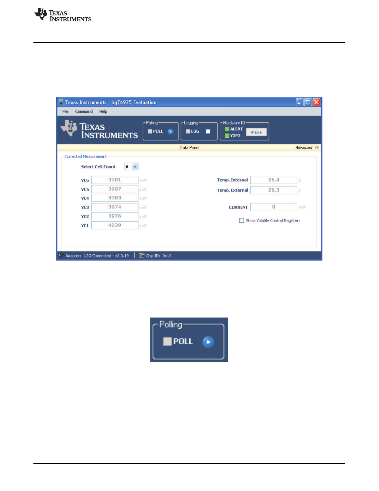
3.5.2 Start Polling Data
Data from the bq76925 can be polled and displayed in the application. To start polling, click on the Poll
button.
With polling active, the cell voltages and temperatures update on a periodic basis. The poll indicator light
next to the word POLL flashes between green and orange for each poll cycle.
Figure 1. Home Screen of the Evaluation Software
Figure 2. Poll Button in the Evaluation Software.
SLUU514–July 2011 bq76925EVM Evaluation Module
Submit Documentation Feedback
Copyright © 2011, Texas Instruments Incorporated
13
Page 14
Quick-Start Demonstration
www.ti.com
Figure 3. Poll Button in the Evaluation Software
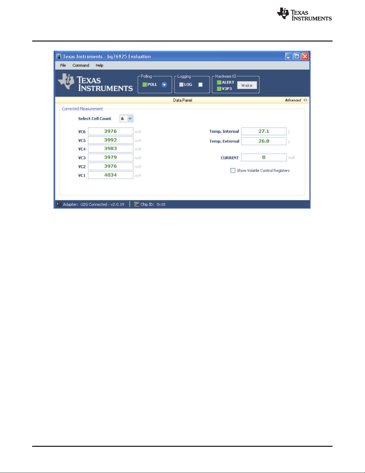
3.5.3 Add Second Power Supply to Simulate Current
One way to easily simulate battery current is to apply a millivolt source to the current-sense inputs of the
bq76925. Tens of amperes can be simulated where each 10 mV is equal to 10 amperes.
14
bq76925EVM Evaluation Module SLUU514– July 2011
Copyright © 2011, Texas Instruments Incorporated
Submit Documentation Feedback
Page 15

+-
24.0V 100mA
Power Supply1
50mV 100mA
Power Supply2
- +
Personal Computer
Windows XP32 Bit
with
bq76925 Evaluation
Software Installed
USB
USB-TO-
GPIO
Adapter
www.ti.com
Quick-Start Demonstration
Figure 4. Demo With Two Power Supplies
Remove the shunt from header J5. Use the second power supply to apply 50 mV between pin 1 of header
J5 and the BATT- terminal. This simulates approximately –50 A or –50,000 mA, of discharge current.
Figure 5. Voltage, Temperature, and Current Measurement in the Evaluation Software
SLUU514–July 2011 bq76925EVM Evaluation Module
Submit Documentation Feedback
Copyright © 2011, Texas Instruments Incorporated
15
Page 16
Control Register Demonstration
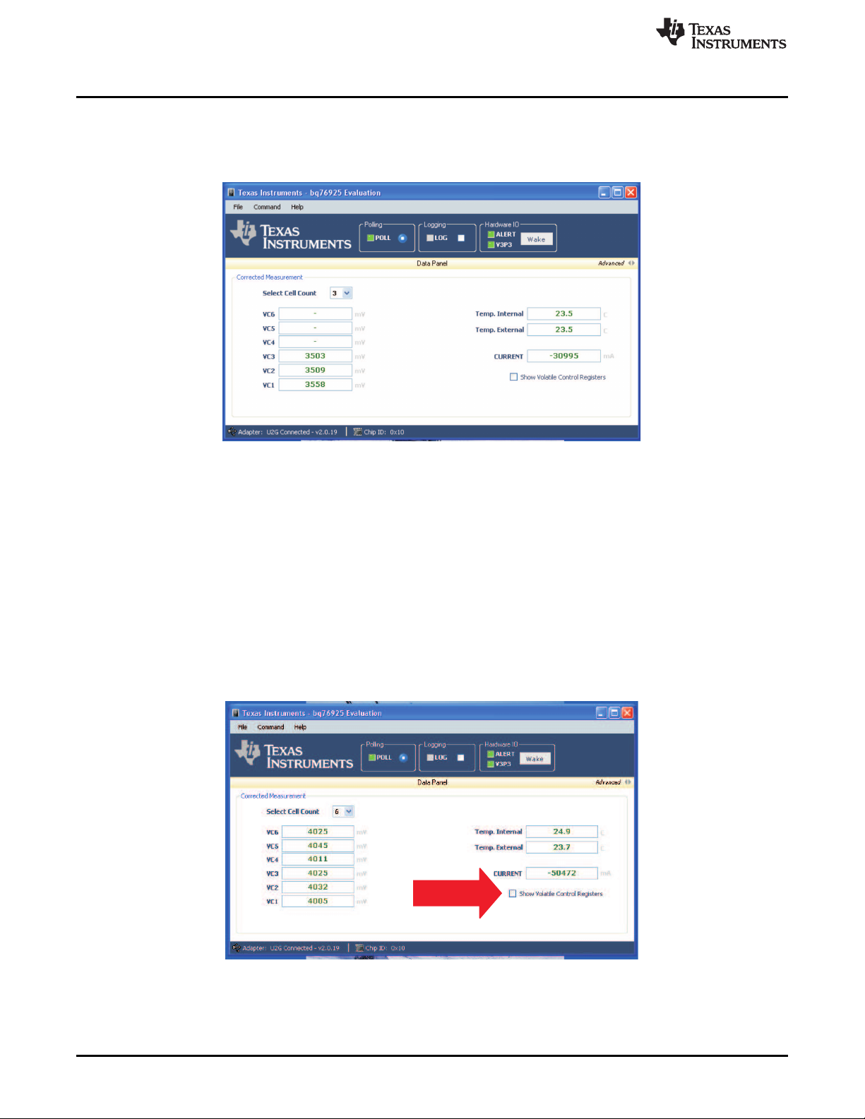
The drop-down box labeled Select Cell Count determines the number of cell voltage measurements that
are displayed: 1 to 6. This function is independent of the cell count. For example, if the user only wanted
to display 3 cells of a 6-cell pack, then the Select Cell Count box is changed to 3. This convenience
feature avoids seeing a somewhat random number being displayed for unconnected cell inputs.
www.ti.com
Figure 6. Select Cell Count Set to Three Cells
4 Control Register Demonstration
The Quick-Start demonstration from the previous section presents the fundamental measurement system
of the bq76925. The method to access and modify the Control Registers using the Evaluation Software is
presented in this section.
4.1 View Control Registers
4.1.1 Introduction
Open the Evaluation Software, if not already open, and click the checkbox marked Show Volatile Control
Registers.
16
Figure 7. Volatile Control Registers Checkbox
This expands the home window to show the six registers.
bq76925EVM Evaluation Module SLUU514– July 2011
Copyright © 2011, Texas Instruments Incorporated
Submit Documentation Feedback
Page 17

www.ti.com
Control Register Demonstration
Figure 8. Volatile Control Registers Access
All of the bits that are assigned for reading and writing are shown. Bit positions that are unnamed are not
used. These bits must always be left as zero.
A legend that can be clicked explains the bit colors. A zero value for a bit is displayed as a grey
background. A one is shown as either a green background or as an orange background.
Clicking each bit toggles the bit value in real time. If a bit turns green, it is set to a 1. If a bit is white or
grey, it is a zero. Each of the STATUS bits is displayed in orange when they are a value of 1.
If the SLEEP bit is a 1, it halts communications, so that the status of this bit is unable to be displayed. The
SLEEP bit always appears to be OFF or MASKED.
SLUU514–July 2011 bq76925EVM Evaluation Module
Submit Documentation Feedback
Copyright © 2011, Texas Instruments Incorporated
17
Page 18

Control Register Demonstration
www.ti.com
Figure 9. Volatile Control Registers Bit Legend
4.1.2 Factory-Programmed Register Values
The Control Registers are programmed at the factory to have a default value. Table 15 shows these
values.
Table 15. Default Register Values
Address Register Default Value
0x00 STATUS 0x01
0x01 CELL_CTL 0x10
0x02 BAL_CTL 0x00
0x03 CONFIG_1 0x00
0x04 CONFIG_2 0x81
0x05 PWR_CTL 0x00
4.1.3 Register Values When Polling
When the Polling button is pressed, the PWR_CTL register is forced to the value of 0x1F. This turns on all
measurement systems as well as the current comparator. This is shown in the Control Register Display.
Note that other bits are automatically updated (written) during polling but are not displayed (read). The
update rate of the bits during polling is in the 10s of milliseconds and does not make sense to display.
4.2 Control Registers Introduction
18
The Control Registers of the bq76925 are used to configure and control the device. A summary of the
read/write Control Registers follows. This user's guide, however, does not provide the necessary details
on the operation and settings of these registers that are given in the bq76925 data sheet . For those
details, see SLUSAM9.
Mousing over a bit in the Control Register section of the software displays a brief description of the bit.
bq76925EVM Evaluation Module SLUU514– July 2011
Copyright © 2011, Texas Instruments Incorporated
Submit Documentation Feedback
Page 19

www.ti.com
4.2.1 STATUS: 0x00
Bit 0 is the Power On Reset Flag (POR). It is set on a each power-up and wake up from sleep.
Bit 1 is the CRC Error Status Flag (CRC_ERROR). It is updated on every I2C write packet.
Bit 2 is the Overcurrent Alert Status Flag (ALERT). This reflects the state of the overcurrent comparator.
4.2.2 CELL_CTL: 0x01
Bits 0-2 are the cell select bits (CELL_SEL) that determine which cell voltage input (VC1 – VC6) is sent to
the VCOUT pin.
Bits 4-5 are the VCOUT multiplexer selector bits (VCOUT_SEL). These bits determine the output of the
VCOUT pin: either VSS, VCn, Vref x 0.5, or Vref x 0.85.
4.2.3 BAL_CTL: 0x02
Bits 0-5 are for cell balance control (BAL_1…BAL_6).
4.2.4 CONFIG_1: 0x03
Bit 0 is the current amplifier gain select bit (I_GAIN). The gain can be set to 4 or 8.
Bit 2 is the current amplifier calibration bit (I_AMP_CAL). It is used to select the current measurement:
from SENSEN or SENSEP.
Bit 3 is the current comparator polarity select bit (I_COMP_POL). This determines the current direction
used to trip the comparator: charge or discharge.
Bits 4 – 7 determine the current comparator threshold setting (I_THRESH). Sixteen different mV levels are
available.
Control Register Demonstration
4.2.5 CONFIG_2: 0x04
Bit 0 is used to set the reference voltage level (REF_SEL). VREF has two different voltage levels.
Bit 7 is used to enable or disable the I2C CRC.
4.2.6 POWER_CTL: 0x05
Bit 0 is used to enable or disable the reference voltage (REF_EN).
Bit 1 is used to enable or disable the thermistors bias voltage (VTB_EN).
Bit 2 is used to enable or disable the cell voltage amplifier (VC_AMP_EN).
Bit 3 is used to enable or disable the current amplifier (I_AMP_EN).
Bit 4 is used to enable or disable the current comparator (ICOMP_EN).
Bit 6 is used to disable the sleep mode (SLEEP_DIS).
Bit 7 is used to enter sleep mode (SLEEP).
4.3 Modifying Control Registers
Control register bits that are writable can be modified by simply clicking on the bit that the user wishes to
change. The modification is immediately communicated by the Evaluation Software to the bq76925.
4.4 Sleep Mode and Wake Up
The bq76925 can be put into a low-power mode called Sleep. Bit 7 in the PWR_CTL register is called
SLEEP. When this bit is set to a 1, the part shuts down the V3P3 output and enters the low-power state.
To enter sleep mode, simply click the SLEEP bit in the Control Registers display.
SLUU514–July 2011 bq76925EVM Evaluation Module
Submit Documentation Feedback
Copyright © 2011, Texas Instruments Incorporated
19
Page 20

Control Register Demonstration
The bq76925 shuts down the 3.3-V level at the V3P3 pin. The Hardware IO section shows a red light next
to V3P3 to indicate that the 3.3-V level is now zero. The Evaluation Software actually monitors the V3P3
output of the bq76925 via the USB-TO-GPIO Adapter input on pin 1.
www.ti.com
Figure 10. Sleep Mode Showing 3.3-V Status
The method to wake the part from sleep is to apply a voltage, 3.3 V in the case of the bq76925EVM, to
the ALERT pin. This is accomplished easily by clicking the Wake button in the Hardware IO Section.
20
Figure 11. Wake Up From Sleep Mode
bq76925EVM Evaluation Module SLUU514– July 2011
Copyright © 2011, Texas Instruments Incorporated
Submit Documentation Feedback
Page 21

www.ti.com
5 Control Panel Demonstration
The Control Panel features of the bq76925 Evaluation Software are explained in this section. This is a
deeper look in to the software operation and the functionality of the bq76925.
5.1 Access to the Control Panel
The Control Panel is purposefully hidden from view when the software is first opened. This approach
eases the user into the complexity of the software. Access to the control panel is gained by clicking on the
small toggle switch in the top right corner of the home screen labeled Advanced.
Control Panel Demonstration
Figure 12. Open Control Panel
Figure 13. Control Panel Details
SLUU514–July 2011 bq76925EVM Evaluation Module
Submit Documentation Feedback
Copyright © 2011, Texas Instruments Incorporated
21
Page 22

Control Panel Demonstration
5.2 Measurement Tab
The measurement menu includes an Analog Output section and EEPROM Correction Registers section as
shown in Figure 14.
www.ti.com
Figure 14. Measurement Tab in the Control Panel
5.3 Analog Output Section
The Analog Output Section consists primarily of a display of the analog outputs of the bq76925 circuit
including VCOUT, VIOUT, VREF, and THERM.
The analog levels are measured by the onboard MSP430F2122 and then stored internally. The MSP430
updates all of the analog-to-digital converter (A/D) results on a 12-µs interval. The bq76925 software
writes to the control registers in the bq76925 to dictate how the measurement system operates. The
sequence of events is as follows:
1. Set VCOUT to Read Internal Temperature.
2. Delay 40 µs, get A/D Counts for Internal Temperature.
3. Set VCOUT to Read VC6.
4. Delay 40 µs, get A/D Counts for VC6.
5. Set VCOUT to Read VC5.
6. Delay 40 µs, get A/D Counts for VC5.
7. Set VCOUT to Read VC4.
8. Delay 40 µs, get A/D Counts for VC4.
9. Set VCOUT to Read VC3.
10. Delay 40 µs, get A/D Counts for VC3.
11. Set VCOUT to Read VC2.
22
bq76925EVM Evaluation Module SLUU514– July 2011
Copyright © 2011, Texas Instruments Incorporated
Submit Documentation Feedback
Page 23

1317 VCOUT
4.018
-
æ ö
ç ÷
è ø
( )
VREF
VCOUT
VC6 GC + VC6_OFFSET_CORR 0.001
1 + VC6_GAIN_CORR 0.001
G
æ ö
´ ´
´ ´
ç ÷
è ø
( )
VREF
VCOUT
VC5 GC + VC5_OFFSET_CORR 0.001
1 + VC5_GAIN_CORR 0.001
G
æ ö
´ ´
´ ´
ç ÷
è ø
( )
VREF
VCOUT
VC4 GC + VC4_OFFSET_CORR 0.001
1 + VC4_GAIN_CORR 0.001
G
æ ö
´ ´
´ ´
ç ÷
è ø
( )
VREF
VCOUT
VC3 GC + VC3_OFFSET_CORR 0.001
1 + VC3_GAIN_CORR 0.001
G
æ ö
´ ´
´ ´
ç ÷
è ø
( )
VREF
VCOUT
VC2 GC + VC2_OFFSET_CORR 0.001
1 + VC2_GAIN_CORR 0.001
G
æ ö
´ ´
´ ´
ç ÷
è ø
( )
VREF
VCOUT
VC1 GC + VC1_OFFSET_CORR 0.001
1 + VC1_GAIN_CORR 0.001
G
æ ö
´ ´
´ ´
ç ÷
è ø
( )
VREF
NOMINAL
VREF_OFFSET_CORR 0.001
GC = 1 + VREF_GAIN_CORR 0.001 +
VREF
´
´
www.ti.com
12. Delay 40 µs, get A/D Counts for VC2.
13. Set VCOUT to Read VC1.
14. Delay 40 µs, get A/D Counts for VC1.
15. Set VIOUT to read SENSEP (SENSEN for first 5 s of polling).
16. Delay 40 µs, get A/D Counts for Current.
17. Get A/D Count for THERM.
5.4 VCOUT Readings
VCOUT is a multiplexed output, and up to seven measurement results can be displayed. These millivolt
values are converted to Corrected Measurements on the home screen using the equations in Table 16.
Display Function Formula to convert VCOUT reading to Cell Voltage or Temperature Units
Name
Tint Internal Temp. °C
VC6 Cell 6 mV
VC5 Cell 5 mV
Control Panel Demonstration
Table 16. Formulas to Convert VCOUT to either °C or mV
VC4 Cell 4 mV
VC3 Cell 3 mV
VC2 Cell 2 mV
VC1 Cell 1 mV
In Table 16, GC
And, G
VCOUT
REF
must be set to 0.6 for the bq76925EVM.
The VCn in Table 16 is the millivolt reading shown in the measurement window.
5.5 VIOUT Readings
The VIOUT readings are shown in millivolts and labeled as SENSEP and SENSEN. The SENSEN
readings are done with I_AMP_CAL set to zero and are only taken in the first 5 seconds of polling while
the VIOUT signal level stabilizes. After that time, SENSEN is not updated. The SENSEP readings are
done with I_AMP_CAL set to one thereafter and are done continuously until polling is stopped.
This measurement technique results in an approximate 5-s delay before the current measurement
stabilizes.
is defined as
(1)
5.6 Auto Control
Two checkboxes are in the Analog Output Section: Auto Control VCOUT during poll and Auto Control
VIOUT during poll, checked by default. The Auto Control VCOUT During Poll means that all six-cell
voltage inputs are read during polling. The Auto Control VIOUT During Poll means that the current is read
during polling. Note that these checkboxes do not turn the Voltage and Current Amplifier circuits on/off.
SLUU514–July 2011 bq76925EVM Evaluation Module
Submit Documentation Feedback
Copyright © 2011, Texas Instruments Incorporated
23
Page 24

A
B
C
D
E
F
H
F
Control Panel Demonstration
5.7 EEPROM Correction Registers
The EEPROM Correction Registers are the seven registers in the bq76925 that store the offset and gain
values for the VCn circuits and the VREF circuit. These values can be different for each device. See the
data sheet for additional details.
Each gain value is derived from the top four bits (nibble) of the register value. This number is a signed 2’s
complement representation in the range of –8 to +7. The units are in mV.
Each offset value is derived from the bottom four bits (nibble) of the register value. This number is a
signed 2’s complement representation. The units are in 0.1%.
5.8 Startup Config Tab
The Startup Config tab is a convenience feature. It allows the user to set the way the bq76925 Evaluation
Software initializes each time it is started or when the Find Target Command is issued.
This tab specifies the settings of the Control Registers 0x00 to 0x05 when the Enable checkbox is
checked.
www.ti.com
Figure 15. Startup Config Tab in the Control Panel
5.9 Configuration Control
The Configuration Control section displays some of the options that a user may want to have preselected
each time the software starts. The features are listed by description rather than bit location and value (1 or
0). Again, this is a convenience feature, and usage of this tab is purely optional.
(A) A drop-down box for the Current Comparator threshold setting has values of 25, 50, 75, … , 375, 400
mV. These are bits 4 to 7 in the CONFIG_1 register.
(B) Two radio buttons allow the user to select the current polarity for the Current Comparator Threshold.
This is bit 3 of the CONFIG_1 register.
24
bq76925EVM Evaluation Module SLUU514– July 2011
Copyright © 2011, Texas Instruments Incorporated
Submit Documentation Feedback
Page 25

www.ti.com
(C) A drop-down box for the Current Amplifier Gain is bit 0 of the CONFIG_1 register.
(D) Two radio buttons allow the user to select the current measurement polarity for the Current Amplifier.
This is bit 2 of the CONFIG_1 register.
(E) Two radio buttons allow the user to select the voltage reference (VREF). This is bit 0 of the CONFIG_2
register.
(F) The CRC Enable/Disable function has a checkbox. Check the box marked CRC Enable to turn on the
CRC feature. This is bit 7 of the CONFIG_2 register.
(G) The POR Enable/Disable function has a checkbox. Check the box marked POR Clear to turn on the
POR clear feature. This is related to bit 0 of the CONFIG_1 register.
(H) The Startup Config Functionality has a checkbox to enable/disable.
5.9.1 Configuration Control Example
As an example of how to use the Configuration Control, change the Current Comparator Threshold to 175
mV, and then press the F2 key to execute the Find Target Command. The I_THRESH bits in the
CONFIG_1 register changes to [0110].
Control Panel Demonstration
Figure 16. Change to the Current Comparator Threshold to 175 mV at Start-Up
5.10 Power Control
The Power Control section allows the user to have certain components of the measurement system
enabled at the start of the software.
When checked, five checkboxes activate the corresponding components in the bq76925. The default
setting is to have all of the components turned off.
These checkboxes correspond to bits 0 to 4 in the PWR_CTL register.
5.11 Logging Tab
The logging tab is another convenience feature. It allows the user to record the I2C transactions that take
place between the bq76925 software and the bq76925.
SLUU514–July 2011 bq76925EVM Evaluation Module
Submit Documentation Feedback
Copyright © 2011, Texas Instruments Incorporated
25
Page 26

Control Panel Demonstration
5.12 Log File
www.ti.com
Figure 17. The Logging Tab
Three buttons specify the file to be used during logging.
1. The Browse… button opens a dialog box to let the user choose an existing log file to use to record the
logged data.
2. The Create… button opens a dialog box to let the user create an existing log file to use to record the
logged data.
3. The Export… button opens the file listed in the text box preceded by Log File: in the program assigned
to open Common Separated Value (.csv) files on the computer. Typically, this is a Microsoft Excel™
file.
5.13 Log File Options
The logging rate can be set by the drop-down box marked Log Rate. The logging rates are in seconds.
Two checkboxes offer options for how logging is done. The first checkbox labeled Overwrite File deletes
any existing data in the specified log file (.csv) each time logging is started. The second checkbox labeled
Include Uncorrected Values includes all of the uncorrected values for VCOUT and VIOUT.
5.14 Enable/Disable Logging
Logging is enabled by clicking the checkbox on the home screen of the software marked Logging. Then,
only after polling is started does the log file start to record samples of data. Logging is halted when polling
is stopped.
Editing of the Logging Tab is disabled when logging is enabled.
5.15 Log File Example
Table 17 is an example of a log file recording. This file only includes the corrected data.
Table 17. Example Log File
TimeStamp VC6 VC5 VC4 VC3 VC2 VC1 Current
6/15/2011 9:52 3953 3935 3878 3943 3949 3944 27.4 26.8 –722
6/15/2011 9:52 3953 3940 3878 3938 3949 3940 27.4 26.7 –722
26
bq76925EVM Evaluation Module SLUU514– July 2011
Copyright © 2011, Texas Instruments Incorporated
Int. Ext.
Temperature Temperature
Submit Documentation Feedback
Page 27

www.ti.com
Control Panel Demonstration
Table 17. Example Log File (continued)
TimeStamp VC6 VC5 VC4 VC3 VC2 VC1 Current
6/15/2011 9:52 3948 3940 3878 3938 3949 3944 27.4 26.3 –722
6/15/2011 9:52 3948 3940 3878 3938 3949 3944 27.4 26.7 –722
6/15/2011 9:52 3953 3940 3878 3938 3949 3940 27.4 26.7 –722
6/15/2011 9:52 3948 3940 3878 3938 3949 3944 27.4 26.1 –722
6/15/2011 9:52 3948 3940 3878 3943 3949 3935 27.4 26.9 –722
6/15/2011 9:52 3953 3940 3878 3943 3949 3940 27.4 26.8 –722
6/15/2011 9:52 3953 3940 3878 3938 3949 3944 28.2 26.8 –722
6/15/2011 9:52 3953 3940 3878 3938 3949 3944 27.4 26.9 –722
6/15/2011 9:52 3948 3940 3878 3938 3949 3940 27.4 26.7 –33922
6/15/2011 9:52 3943 3940 3878 3934 3949 3944 27.4 26.7 –47635
6/15/2011 9:52 3953 3940 3878 3938 3949 3944 27.4 26.8 –49800
6/15/2011 9:53 3948 3935 3878 3938 3949 3944 27.4 26.8 –49800
6/15/2011 9:53 3948 3940 3878 3943 3949 3944 27.4 26.8 –49800
6/15/2011 9:53 3953 3940 3878 3943 3949 3944 27.4 26.8 –50522
6/15/2011 9:53 3948 3940 3873 3938 3949 3940 27.4 26.9 –49800
6/15/2011 9:53 3953 3940 3878 3938 3949 3944 27.4 26.8 –49800
6/15/2011 9:53 3948 3940 3878 3938 3949 3944 27.4 26.8 –49800
6/15/2011 9:53 3948 3940 3878 3943 3949 3944 27.4 26.8 –50522
Int. Ext.
Temperature Temperature
5.16 Communications Tab
The communications tab is another convenience feature of the bq76925 Evaluation Software. It gives the
user insight into the communications happening between the Software, MSP430F2122, and the bq76925.
It also allows the user to perform manual reads and writes of the control registers of the bq76925.
The software both writes and reads to the bq76925 and just reads from the MSP430F2122.
Figure 18. Communications Tab
5.17 Monitor Window
The Monitor window can be used to monitor all of the communication traffic on the I2C bus. It records the
transaction history. The default condition of the monitor is to be off. Click on the checkbox below the
window that is labeled Enable to enable the monitor.
The Clear button erases the contents of the monitor window, if clicked.
SLUU514–July 2011 bq76925EVM Evaluation Module
Submit Documentation Feedback
Copyright © 2011, Texas Instruments Incorporated
27
Page 28

Control Panel Demonstration
CAUTION
Be aware of a warning that reads: "Attention. The purpose of this
communications monitor is to evaluate the various commands to and from the
target device. It is not recommended for long term data capture and should be
disabled while logging is active.” This restriction is computer dependent based
on the amount of system memory. If left on for too long, the computer’s system
memory may get allocated to a point where the application performance can be
severely affected.
I2C_W is a write transaction from the software. I2C_R is a read transaction issued by the software.
5.18 Transactions During a Connect to Device Command
The typical transaction history after a Connect to Device command appears as shown in Table 18:
Table 18. Example of a Device Connect Command
Searching for I2C device...
I2C_R: 20 1 49
Device found!
Base Address: 0x20
I2C_W: 21 10 1
I2C_R: 21 10 14
I2C_R: 20 1 49
I2C_W: 23 0 25
I2C_R: 23 0 30
I2C_R: 20 1 49
I2C_W: 24 81 7D
I2C_R: 24 81 68
I2C_R: 20 1 49
I2C_W: 25 0 D9
I2C_R: 25 0 CC
I2C_R: 20 1 49
I2C_R: 20 1 49
I2C_R: 21 10 14
I2C_R: 22 0 1A
I2C_R: 23 0 30
I2C_R: 24 81 68
I2C_R: 25 0 CC
I2C_R: 27 10 E8
I2C_R: 30 3F 5D
I2C_R: 31 10 BA
I2C_R: 32 10 C4
I2C_R: 33 30 0E
I2C_R: 34 4F A2
I2C_R: 35 4E 8F
I2C_R: 36 4D F8
www.ti.com
28
bq76925EVM Evaluation Module SLUU514– July 2011
Copyright © 2011, Texas Instruments Incorporated
Submit Documentation Feedback
Page 29

www.ti.com
First column is a comment. Second column is the combined device-address and register-address. Third
column is the register value. Last column is the CRC.
5.19 I2C
The I2C section shows the I2C Base Address of the bq76925 and the group address. These are 0x20 and
0x04, respectively. The base address is the group address shifted to the left by three places.
The user can use this I2C section to read and write data to the bq76925.
5.20 I2C Register Read
To read a register, select the desired register to read using the drop-down box. Refer to the product data
sheet to understand the meaning and usage of each register. Then click the Read button. The result is
displayed in the Monitor window.
For example, a read of register 0x01, CELL_CTL, appear as:
I2C_R: SPACER 22 SPACER 00 SPACER 1A.
The first number, 0x22, is the combined device address and the register number. The second number,
0x00, is the value of the register. The third number, 0x1A, is the CRC. If the CRC_EN bit in the
CONFIG_2 register is not set, the CRC value 0x1A does not appear.
5.21 I2C Register Write
To write a register, select the desired register to write using the drop-down box. See the product data
sheet to understand the meaning and usage of each register. Enter the value to be written in hexadecimal
notation. Then click the Write button. The result is displayed in the Monitor window.
If the Update GUI on write checkbox is selected, then the change to the register is updated in the Volatile
Control Registers section.
Control Panel Demonstration
5.22 I2C Communications With MSP430F2122
The I2C device address of the MSP430F2122 was assigned as 0x40 so as to not interfere with the
address structure of the bq76925.
The MSP430 reads the various analog outputs of the bq76925 and stores the results, in terms of counts,
in registers in its memory. The MSP430 A/D converter has 10 bits of resolution. The software accesses
these registers. The register map inside the MSP430 is shown in Table 19.
Table 19. Data From MSP430F2122
Byte
Number
1 Status of Alert pin: None
2 Reserved Reserved None
Name Description Units
Status of Alert pin. Bit zero indicates level
1=High, 0=Low (Overcurrent).
SLUU514–July 2011 bq76925EVM Evaluation Module
Submit Documentation Feedback
Copyright © 2011, Texas Instruments Incorporated
29
Page 30

Control Panel Demonstration
Table 19. Data From MSP430F2122 (continued)
Byte
Number
3 Ext Thermistor, MSB
4 Ext Thermistor, LSB
5 VCOUT, MSB
6 VCOUT, LSB
7 VIOUT1, MSB
8 VIOUT1, LSB
9 VIOUT2, MSB
10 VIOUT2, LSB
11 VREF, MSB
12 VREF, LSB
13 1/2 x DVCC, MSB
14 1/2 x DVCC, LSB
Name Description Units
Thermistor voltage
VCOUT voltage
VIOUT1 voltage (current)
VIOUT2 voltage
VREF voltage
DVCC voltage
To convert to mV, divide the 10-bit value by 1024 and multiply by the reference voltage (VREF) of 3000
mV.
5.23 Example of I2C Communications from MSP430F2122
The software continuously accesses the MSP430 registers during polling. An example of this appears in
Table 20.
www.ti.com
Counts from 10-bit A/D converter
Table 20. Example of a Device Connect Command
I2C_W: 25 1F 84
I2C_R: 25 1F 91
I2C_W: 21 16 13
I2C_R: 40 0 0 2 30 1 9E 0 77 0 77 3 FF 2 2B
I2C_W: 21 15 1A
I2C_R: 40 0 0 2 30 3 36 0 AC 0 AB 3 FE 2 2F
I2C_W: 21 14 1D
I2C_R: 40 0 0 2 30 3 33 0 DB 0 DA 3 FF 2 2E
I2C_W: 21 13 8
I2C_R: 40 0 0 2 30 3 26 1 5 0 FA 3 FE 2 30
I2C_W: 21 12 0F
I2C_R: 40 0 0 2 30 3 32 1 22 1 21 3 FF 2 2F
I2C_W: 21 11 6
I2C_R: 40 0 0 2 30 3 35 1 45 1 44 3 FF 2 2E
I2C_W: 21 10 1
I2C_R: 40 0 0 2 30 3 2F 1 64 1 64 3 FE 2 30
I2C_W: 23 0 25
I2C_R: 40 0 0 2 2F 3 30 1 81 1 81 3 FF 2 2F
I2C_W: 21 16 13
I2C_R: 40 0 0 2 2F 1 9E 1 D6 1 D6 3 FF 2 2F
I2C_W: 21 15 1A
I2C_R: 40 0 0 2 30 3 36 1 E9 1 E8 3 FF 2 2F
I2C_W: 21 14 1D
I2C_R: 40 0 0 2 30 3 34 1 F9 1 F9 3 FF 2 2E
I2C_W: 21 13 8
I2C_R: 40 0 0 2 30 3 26 2 6 2 7 3 FF 2 2F
30
bq76925EVM Evaluation Module SLUU514– July 2011
Copyright © 2011, Texas Instruments Incorporated
Submit Documentation Feedback
Page 31

www.ti.com
In general, polling data involves writing to the Control Registers of the bq76925 to configure the outputs
(VCOUT, VIOUT and VTB) and then reading the results from the MSP430.
3-, 4-, and 5-Cell Operation
Table 20. Example of a Device Connect Command (continued)
I2C_W: 21 12 0F
I2C_R: 40 0 0 2 30 3 32 2 15 2 15 3 FF 2 2D
I2C_W: 21 11 6
I2C_R: 40 0 0 2 30 3 35 2 21 2 21 3 FF 2 2F
I2C_W: 21 10 1
I2C_R: 40 0 0 2 30 3 2F 2 2C 2 2C 3 FF 2 2E
I2C_W: 23 0 25
I2C_R: 40 0 0 2 2F 3 2F 2 36 2 34 3 FE 2 30
I2C_W: 25 0 D9
I2C_R: 25 0 CC
I2C_W: 21 10 1
I2C_R: 40 0 0 2 30 3 2F 2 2C 2 2C 3 FF 2 2E
I2C_W: 23 0 25
I2C_R: 40 0 0 2 2F 3 2F 2 36 2 34 3 FE 2 30
I2C_W: 25 0 D9
I2C_R: 25 0 CC
6 3-, 4-, and 5-Cell Operation
This section includes instructions for setting up the bq76925EVM for operation with less than 6 cells. The
discussion considers operation with the cell simulator only.
6.1 Introduction
The bq76925 is capable of working with cell packs that have 3-, 4-, 5-, or 6-series connected cells. There
are some special considerations when operating with less than six series cells. For complete information,
consult the bq76925 data sheet.
Configure the bq76925EVM for the appropriate cell count prior to applying
power to the board.
6.2 Using Onboard Cell Simulator
The cell simulator can be set up for 3-, 4-, 5-, or 6-cell operation. The process simply involves placing a
shorting wire across the proper pins on the CN6:CELLS connector.
6.3 Five-Cell Operation
The procedure for five-cell operation with the simulation circuit is as follows:
1. Ensure that the power to the board, at BATT+/-, is removed.
2. Close all switches on S4.
3. Apply a jumper wire from pin 1 to pin 2 on connector CN6. These are the inputs marked Cell 6 and
Cell 5.
4. Set the power supply to a safe level for 5-cell operation. This is somewhere below 25 V.
5. Connect the power supply to BATT+ and BATT–.
6. Turn on the power supply.
7. Connect to the evaluation software.
CAUTION
SLUU514–July 2011 bq76925EVM Evaluation Module
Submit Documentation Feedback
Copyright © 2011, Texas Instruments Incorporated
31
Page 32

Operation With Cells
8. Change the Select Cell Count drop-down box on the home screen to 5.
6.4 Four-Cell Operation
The procedure for four-cell operation with the simulation circuit is as follows:
1. Ensure that the power to the board, at BATT+/–, is removed.
2. Close all switches on S4.
3. Apply a jumper wire from pin 1 to pin 2 on connector CN6. These are the inputs marked Cell 6 and
Cell 5.
4. Apply a jumper wire from pin 2 to pin 3 on connector CN6. These are the inputs marked Cell 5 and
Cell 4.
5. Set the power supply to a safe level for 4-cell operation. This is somewhere below 20 V.
6. Connect the power supply to BATT+ and BATT–.
7. Connect to the evaluation software.
8. Change the Select Cell Count drop-down box on the home screen to 4.
6.5 Three-Cell Operation
The procedure for three-cell operation with the simulation circuit is as follows:
1. Ensure that the power to the board, at BATT+/–, is removed.
2. Close all switches on S4.
3. Apply a jumper wire from pin 1 to pin 2 on connector CN6. These are the inputs marked Cell 6 and
Cell 5.
4. Apply a jumper wire from pin 2 to pin 3 on connector CN6. These are the inputs marked Cell 5 and
Cell 4.
5. Apply a jumper wire from pin 3 to pin 4 on connector CN6. These are the inputs marked Cell 4 and
Cell 3.
6. Set the power supply to a safe level for 4 cell operation. This would be somewhere below 15 V.
7. Connect the power supply to BATT+ and BATT–.
8. Connect to the evaluation software.
9. Change the Select Cell Count drop-down box on the home screen to 3.
www.ti.com
7 Operation With Cells
This section discusses operating the bq76925EVM with a real cell pack.
7.1 Preparing Circuit for Operation
Improper operation with real lithium-ion cells can cause permanent damage to
the bq76925EVM.
No battery current control devices (MOSFETs) are on this EVM that
can stop the flow of charge or discharge current in the event that a
dangerous condition is induced through discharging or charging
of a battery. Exercise extreme caution when using a battery with
this EVM.
32
bq76925EVM Evaluation Module SLUU514– July 2011
Copyright © 2011, Texas Instruments Incorporated
CAUTION
WARNING
Submit Documentation Feedback
Page 33

www.ti.com
Disconnect all external electronics from the bq76925EVM prior to the connection of real cells. This
includes power supplies, electronic load, USB-TO-GPIO Adapter or MSP-FET430UIF that may be
connected.
7.2 Battery Connection Sequence
The connection of a real battery pack to the bq76925EVM requires a certain connection sequence for safe
operation.
The fundamental connection sequence is:
1. Ensure that all switches on S4 are open.
2. Connect BATT–.
3. Connect BATT+.
4. Connect CN6. The cell inputs have a specific assignment (1-1, 2-2, 3-3,etc) but no specific connection
timing sequence is required.
Remove the CN6 mating connector from the board before wiring cell connections to the terminals.
7.3 Six-Cell Operation
The procedure for six-cell operation with a cell pack is as follows:
1. Ensure that all switches on S4 are open.
2. Wire the seven-cell tap wires to the mating plug of CN6.
3. Connect BATT–.
4. Connect BATT+.
5. Connect CN6 to the EVM. The cell inputs can be connected in any order.
6. Connect to the evaluation software.
7. Change the Select Cell Count drop-down box on the home screen to 6.
Operation With Cells
7.4 Five-Cell Operation
The procedure for five-cell operation with a cell pack is as follows:
1. Ensure that all switches on S4 are open.
2. Wire the six-cell tap wires to positions 2 through 7 on the mating plug of CN6.
3. Apply a jumper wire from pin 1 to pin 2 on mating plug of CN6. (These are the inputs marked Cell 6
and Cell 5.)
4. Connect BATT–.
5. Connect BATT+.
6. Connect CN6 to the EVM. The cell inputs can be connected in any order.
7. Connect to the evaluation software.
8. Change the Select Cell Count drop-down box on the home screen to 5.
7.5 Four-Cell Operation
The procedure for four-cell operation with the simulation circuit is as follows:
1. Ensure that all switches on S4 are open.
2. Wire the five-cell tap wires to positions 3 through 7 on the mating plug of CN6.
3. Apply jumper wire from pin 1 to pin 2 on plug for CN6. These are inputs marked Cell 6 and Cell 5.
4. Apply jumper wire from pin 2 to pin 3 on plug for CN6. These are inputs marked Cell 5 and Cell 4.
5. Connect BATT–.
6. Connect BATT+.
7. Connect CN6 to the EVM. The cell inputs can be connected in any order.
8. Connect to the evaluation software.
9. Change the Select Cell Count drop-down box on the home screen to 4.
SLUU514–July 2011 bq76925EVM Evaluation Module
Submit Documentation Feedback
Copyright © 2011, Texas Instruments Incorporated
33
Page 34

Schematic and Bill of Materials
7.6 Three-Cell Operation
The procedure for three-cell operation with the simulation circuit is as follows:
1. Ensure that all switches on S4 are open.
2. Wire the four-cell tap wires to positions 4 through 7 on the mating plug of CN6.
3. Apply jumper wire from pin 1 to pin 2 on plug for CN6. These are inputs marked Cell 6 and Cell 5.
4. Apply jumper wire from pin 2 to pin 3 on plug for CN6. These are inputs marked Cell 5 and Cell 4.
5. Apply jumper wire from pin 3 to pin 4 on plug for CN6. These are inputs marked Cell 4 and Cell 3.
6. Connect BATT–.
7. Connect BATT+
8. Connect CN6 to the EVM. The cell inputs can be connected in any order.
9. Connect to the Evaluation Software.
10. Change the Select Cell Count drop-down box on the home screen to 4.
7.7 Battery Removal Sequence
The removal of the battery from the bq76925EVM requires a certain sequence for safe operation.
The connection removal sequence is:
1. Remove USB-TO-GPIO connector at CN8.
2. Unplug CN6 (CELLS).
3. Remove BATT+ connection.
4. Remove BATT– connection.
www.ti.com
8 Schematic and Bill of Materials
This section includes the schematic and the bill of materials for the bq76925EVM.
34
bq76925EVM Evaluation Module SLUU514– July 2011
Copyright © 2011, Texas Instruments Incorporated
Submit Documentation Feedback
Page 35

www.ti.com
8.1 Schematics
Schematic and Bill of Materials
Figure 19. Schematic – Page 1 of 4
SLUU514–July 2011 bq76925EVM Evaluation Module
Submit Documentation Feedback
Copyright © 2011, Texas Instruments Incorporated
35
Page 36

Schematic and Bill of Materials
www.ti.com
Figure 20. Schematic – Page 2 of 4
Figure 21. Schematic – Page 3 of 4
36
bq76925EVM Evaluation Module SLUU514– July 2011
Copyright © 2011, Texas Instruments Incorporated
Submit Documentation Feedback
Page 37

www.ti.com
Schematic and Bill of Materials
Figure 22. Schematic – Page 4 of 4
8.2 Bill of Materials
Table 21. Bill of Materials
Count RefDes Value Description Size Part Number MFR
1 C9 10 µF Capacitor, Ceramic, 50V, Y5V, –20%/+80% 1210 C3225Y5V1H106Z TDK
1 C10 1.0 µF Capacitor, Ceramic, Low Inductance, 16V, X7R, 10% 0805 Standard Standard
1 C12 0.33 µF Capacitor, Leaded, Metalized 40VAC, ±10% 3.0 x 7.2 mm B32529C334K Epcos
1 C14 470 pF Capacitor, Ceramic, 50V, X7R, 10% 0805 Standard Standard
1 C15 4.7 µF Capacitor, Ceramic, 16V, X7R, 10% 0805 Standard Standard
1 C17 470 nF Capacitor, Ceramic, 50V, C0G, 5% 0805 Standard Standard
1 C19 220 pF Capacitor, Ceramic, 50V, X7R, 10% 0805 Standard Standard
1 C23 10 µF Capacitor, Ceramic, 10V, X7R, 10% 0805 Standard Standard
8 C1-7 C11 1.0 µF Capacitor, Ceramic, 25V, X7R, 10% 0805 Standard Standard
0 C18 C21 DNP Capacitor, Ceramic 0805 Standard Standard
2 C20 C22 0.01 µF Capacitor, Ceramic, 50V, X7R, 10% 0805 Standard Standard
5 C8 C13 C16 0.1 µF Capacitor, Ceramic, 25V, X7R, 10% 0805 Standard Standard
C24-25
1 CN6 Header, RA 7p 300V 8A 9.2x28 mm 395021007 Molex
1 -- Plug for Header CN6 39500-0007 Molex
1 CN7 Header, 2x7 pin, 100mil spacing, Straight, 4 Wall 0.338 x 0.988 inch N2514-6002-RB 3M
1 CN8 Connector, 10 pin Shrouded Vertical 0.388 x 0.400 inch C-5103309-1 Tyco
1 CN5 Header, 4-pin Friction Lock, 100 mil spacing, 0.250 x 0.400 inch 22-11-2042 Molex
4 CN1-4 Terminal, PC Screw #6, 30A 0.310 x 0.507 inch 8199 Keystone
1 D2 Diode, Zener, 30V, 500mW SOD-123 BZT52C30V-13-F Diodes
0 D3 DNP Diode, Zener SOD-123 STD Diodes
1 D4 Diode, Zener, 4.7V, 500mW SOD-123 BZT52C4V7-13-F On Semi
1 D6 Diode, UltraFast Rectifier, 1-A, 200-V SMB MURS120T3 On Semi
1 D7 Diode, Transient Voltage Suppressors 12A, 28V 0.155 x 0.180 inch SMBJ28CA Vishay-Liteon or Bourns
3 D1 D5 D14 Diode, Schottky, 0.5A, 40V SOD-123 MBR0540T1G Micro Commercial Co
6 D8-13 Diode, LED, Red, 100 mA 0805 SML-LXT0805SRW-TR Lumen
3 J1-2 J6 Header, Male 3-pin, 100mil spacing, 0.100 inch x 3 PEC03SAAN Sullies
3 J3-5 Header, Male 2-pin, 100mil spacing, 0.100 inch x 2 PEC02SAAN Sullies
6 -- Shunt, 100-mil, Black 0.100 929950-00 3M
1 Q1 Transistor, DNP Medium Power, 40V, 3A SOT-23 ZXTP25040DFH Exodus
1 Q2 MOSFETs, Pch, –50V, –0.13A, 10 Ω SOT23 BSS84 Fairchild
1 Q3 MOSFETS, Nch, 50V, 0.22A, 3.5 Ω SOT23 BSS138 Fairchild
1 R14 200K Resistor, Chip, 1/10W, 5% 0805 Standard Standard
SLUU514–July 2011 bq76925EVM Evaluation Module
Submit Documentation Feedback
Copyright © 2011, Texas Instruments Incorporated
37
Page 38

Printed-Circuit Board
Table 21. Bill of Materials (continued)
Count RefDes Value Description Size Part Number MFR
1 R17 10K Thermistor, NTC, 10 kΩ 0603 NCP18XH103F03RB Murata
1 R22 4.7K Resistor, Chip, 1/10W, 5% 0805 Standard Standard
1 R24 10 Resistor, Chip, 1/10W, 5% 0805 Standard Standard
1 R32 200 Resistor, Chip, 1/10W, 5% 0805 Standard Standard
1 R36 1.0M Resistor, Chip, 1/10W, 5% 0805 Standard Standard
2 R10-11 1.0k Resistor,Chip, 1/10W, 5% 0805 Standard Standard
7 R1-7 47 Resistor, Chip, 1/10W, 5% 0805 Standard Standard
2 R12 R15 100 Resistor, Chip, 1/10W, 5% 0805 Standard Standard
2 R13 R16 10K Resistor, Chip, 1/10W, 5% 0805 Standard Standard
0 R18-20 DNP Resistor, Chip, 1/10W, 5% 0805 Standard Standard
2 R21 R28 47k Resistor, Chip, 1/10W, 5% 0805 Standard Standard
4 R23 R31 R35 3.3k Resistor, Chip, 1/10W, 5% 0805 Standard Standard
R44
3 R27 R37 R45 0 Resistor, Chip, 1/10W, 5% 0805 Standard Standard
4 R30 R25-26 300 Resistor, Chip, 1/10W, 5% 0805 Standard Standard
R29
2 R34 R33 560K Resistor, Chip, 1/10W, 5% 0805 Standard Standard
6 R38-43 510 Resistor, Chip, 1/8W, 5% 0805 Standard Standard
2 R8-9 0.002 Res, Power Metal Strip, 1W, ±1% 2512 WSL-2512 2L000FEA Vishay Dale
2 S1 S3 Switch, Micro Push Button 12V, 50mA 0.394 x 0.200 inch FSM4JSMA ITT
2 S2 S4 Switch, DIP, SPST, Raised rocker, 8-pos. 0.380 x 0.880 inch 76SB08ST Grayhill
29 TP1-29 Test Point, Black, Thru Hole 0.125 x 0.125 inch 5011 Keystone
1 U1 IC, Host Controlled Analog Front End /Battery Protection TSSOP-20 BQ76925PW TI
1 U2 IC, Mixed Signal Microcontroller PW28 MSP430F2122IPW TI
1 -- PCB, 6 In x 3 In x 0.062 In PWR008 Any
and Gas Gage
www.ti.com
9 Printed-Circuit Board
This section includes the plots of the printed-circuit board layers.
38
Figure 23. Top Silkscreen Layer
bq76925EVM Evaluation Module SLUU514– July 2011
Copyright © 2011, Texas Instruments Incorporated
Submit Documentation Feedback
Page 39

www.ti.com
Printed-Circuit Board
Figure 24. Top Copper Layer
Figure 25. Inner Copper Layer
SLUU514–July 2011 bq76925EVM Evaluation Module
Submit Documentation Feedback
Copyright © 2011, Texas Instruments Incorporated
39
Page 40

Printed-Circuit Board
www.ti.com
Figure 26. Inner Copper Layer
40
Figure 27. Bottom Copper Layer
bq76925EVM Evaluation Module SLUU514– July 2011
Copyright © 2011, Texas Instruments Incorporated
Submit Documentation Feedback
Page 41

www.ti.com
Printed-Circuit Board
Figure 28. Drill Drawing
SLUU514–July 2011 bq76925EVM Evaluation Module
Submit Documentation Feedback
Copyright © 2011, Texas Instruments Incorporated
41
Page 42

Evaluation Board/Kit Important Notice
Texas Instruments (TI) provides the enclosed product(s) under the following conditions:
This evaluation board/kit is intended for use for ENGINEERING DEVELOPMENT, DEMONSTRATION, OR EVALUATION
PURPOSES ONLY and is not considered by TI to be a finished end-product fit for general consumer use. Persons handling the
product(s) must have electronics training and observe good engineering practice standards. As such, the goods being provided are
not intended to be complete in terms of required design-, marketing-, and/or manufacturing-related protective considerations,
including product safety and environmental measures typically found in end products that incorporate such semiconductor
components or circuit boards. This evaluation board/kit does not fall within the scope of the European Union directives regarding
electromagnetic compatibility, restricted substances (RoHS), recycling (WEEE), FCC, CE or UL, and therefore may not meet the
technical requirements of these directives or other related directives.
Should this evaluation board/kit not meet the specifications indicated in the User’s Guide, the board/kit may be returned within 30
days from the date of delivery for a full refund. THE FOREGOING WARRANTY IS THE EXCLUSIVE WARRANTY MADE BY
SELLER TO BUYER AND IS IN LIEU OF ALL OTHER WARRANTIES, EXPRESSED, IMPLIED, OR STATUTORY, INCLUDING
ANY WARRANTY OF MERCHANTABILITY OR FITNESS FOR ANY PARTICULAR PURPOSE.
The user assumes all responsibility and liability for proper and safe handling of the goods. Further, the user indemnifies TI from all
claims arising from the handling or use of the goods. Due to the open construction of the product, it is the user’s responsibility to
take any and all appropriate precautions with regard to electrostatic discharge.
EXCEPT TO THE EXTENT OF THE INDEMNITY SET FORTH ABOVE, NEITHER PARTY SHALL BE LIABLE TO THE OTHER
FOR ANY INDIRECT, SPECIAL, INCIDENTAL, OR CONSEQUENTIAL DAMAGES.
TI currently deals with a variety of customers for products, and therefore our arrangement with the user is not exclusive.
TI assumes no liability for applications assistance, customer product design, software performance, or infringement of
patents or services described herein.
Please read the User’s Guide and, specifically, the Warnings and Restrictions notice in the User’s Guide prior to handling the
product. This notice contains important safety information about temperatures and voltages. For additional information on TI’s
environmental and/or safety programs, please contact the TI application engineer or visit www.ti.com/esh.
No license is granted under any patent right or other intellectual property right of TI covering or relating to any machine, process, or
combination in which such TI products or services might be or are used.
FCC Warning
This evaluation board/kit is intended for use for ENGINEERING DEVELOPMENT, DEMONSTRATION, OR EVALUATION
PURPOSES ONLY and is not considered by TI to be a finished end-product fit for general consumer use. It generates, uses, and
can radiate radio frequency energy and has not been tested for compliance with the limits of computing devices pursuant to part 15
of FCC rules, which are designed to provide reasonable protection against radio frequency interference. Operation of this
equipment in other environments may cause interference with radio communications, in which case the user at his own expense
will be required to take whatever measures may be required to correct this interference.
EVM Warnings and Restrictions
It is important to operate this EVM within the input voltage range of 4.2 V to 26.4 V and the output voltage range of 4.2 V to 26.4 V
.
Exceeding the specified input range may cause unexpected operation and/or irreversible damage to the EVM. If there are
questions concerning the input range, please contact a TI field representative prior to connecting the input power.
Applying loads outside of the specified output range may result in unintended operation and/or possible permanent damage to the
EVM. Please consult the EVM User's Guide prior to connecting any load to the EVM output. If there is uncertainty as to the load
specification, please contact a TI field representative.
During normal operation, some circuit components may have case temperatures greater than 60° C. The EVM is designed to
operate properly with certain components above 60° C as long as the input and output ranges are maintained. These components
include but are not limited to linear regulators, switching transistors, pass transistors, and current sense resistors. These types of
devices can be identified using the EVM schematic located in the EVM User's Guide. When placing measurement probes near
these devices during operation, please be aware that these devices may be very warm to the touch.
Mailing Address: Texas Instruments, Post Office Box 655303, Dallas, Texas 75265
Copyright © 2011, Texas Instruments Incorporated
Page 43

IMPORTANT NOTICE
Texas Instruments Incorporated and its subsidiaries (TI) reserve the right to make corrections, modifications, enhancements, improvements,
and other changes to its products and services at any time and to discontinue any product or service without notice. Customers should
obtain the latest relevant information before placing orders and should verify that such information is current and complete. All products are
sold subject to TI’s terms and conditions of sale supplied at the time of order acknowledgment.
TI warrants performance of its hardware products to the specifications applicable at the time of sale in accordance with TI’s standard
warranty. Testing and other quality control techniques are used to the extent TI deems necessary to support this warranty. Except where
mandated by government requirements, testing of all parameters of each product is not necessarily performed.
TI assumes no liability for applications assistance or customer product design. Customers are responsible for their products and
applications using TI components. To minimize the risks associated with customer products and applications, customers should provide
adequate design and operating safeguards.
TI does not warrant or represent that any license, either express or implied, is granted under any TI patent right, copyright, mask work right,
or other TI intellectual property right relating to any combination, machine, or process in which TI products or services are used. Information
published by TI regarding third-party products or services does not constitute a license from TI to use such products or services or a
warranty or endorsement thereof. Use of such information may require a license from a third party under the patents or other intellectual
property of the third party, or a license from TI under the patents or other intellectual property of TI.
Reproduction of TI information in TI data books or data sheets is permissible only if reproduction is without alteration and is accompanied
by all associated warranties, conditions, limitations, and notices. Reproduction of this information with alteration is an unfair and deceptive
business practice. TI is not responsible or liable for such altered documentation. Information of third parties may be subject to additional
restrictions.
Resale of TI products or services with statements different from or beyond the parameters stated by TI for that product or service voids all
express and any implied warranties for the associated TI product or service and is an unfair and deceptive business practice. TI is not
responsible or liable for any such statements.
TI products are not authorized for use in safety-critical applications (such as life support) where a failure of the TI product would reasonably
be expected to cause severe personal injury or death, unless officers of the parties have executed an agreement specifically governing
such use. Buyers represent that they have all necessary expertise in the safety and regulatory ramifications of their applications, and
acknowledge and agree that they are solely responsible for all legal, regulatory and safety-related requirements concerning their products
and any use of TI products in such safety-critical applications, notwithstanding any applications-related information or support that may be
provided by TI. Further, Buyers must fully indemnify TI and its representatives against any damages arising out of the use of TI products in
such safety-critical applications.
TI products are neither designed nor intended for use in military/aerospace applications or environments unless the TI products are
specifically designated by TI as military-grade or "enhanced plastic." Only products designated by TI as military-grade meet military
specifications. Buyers acknowledge and agree that any such use of TI products which TI has not designated as military-grade is solely at
the Buyer's risk, and that they are solely responsible for compliance with all legal and regulatory requirements in connection with such use.
TI products are neither designed nor intended for use in automotive applications or environments unless the specific TI products are
designated by TI as compliant with ISO/TS 16949 requirements. Buyers acknowledge and agree that, if they use any non-designated
products in automotive applications, TI will not be responsible for any failure to meet such requirements.
Following are URLs where you can obtain information on other Texas Instruments products and application solutions:
Products Applications
Audio www.ti.com/audio Communications and Telecom www.ti.com/communications
Amplifiers amplifier.ti.com Computers and Peripherals www.ti.com/computers
Data Converters dataconverter.ti.com Consumer Electronics www.ti.com/consumer-apps
DLP® Products www.dlp.com Energy and Lighting www.ti.com/energy
DSP dsp.ti.com Industrial www.ti.com/industrial
Clocks and Timers www.ti.com/clocks Medical www.ti.com/medical
Interface interface.ti.com Security www.ti.com/security
Logic logic.ti.com Space, Avionics and Defense www.ti.com/space-avionics-defense
Power Mgmt power.ti.com Transportation and www.ti.com/automotive
Microcontrollers microcontroller.ti.com Video and Imaging www.ti.com/video
RFID www.ti-rfid.com Wireless www.ti.com/wireless-apps
RF/IF and ZigBee® Solutions www.ti.com/lprf
TI E2E Community Home Page e2e.ti.com
Automotive
Mailing Address: Texas Instruments, Post Office Box 655303, Dallas, Texas 75265
Copyright © 2011, Texas Instruments Incorporated
Page 44

Mouser Electronics
Authorized Distributor
Click to View Pricing, Inventory, Delivery & Lifecycle Information:
Texas Instruments:
BQ76925EVM
 Loading...