

Page 1

User's Guide
SLUUB03–April 2014
bq51020EVM (5-W WPC) Integrated Wireless Receiver
Power Supply
The bq51020EVM-520 (PWR520-002) wireless power receiver evaluation kit (EVM) from TI is a high
performance, easy-to-use development kit for the design of wireless power solutions. It helps designers to
evaluate the operation and performance of the bq51020 IC, a secondary-side receiver device for wireless
power transfer in portable applications. The bq51020 device is a fully-contained, wireless power receiver
capable of operating in WPC v1.1 protocol which allows a wireless power system to deliver up to 5 W to
the system when used with a Qi inductive transmitter. The bq51020 device provides a single device power
conversion (rectification and regulation) as well as the digital control and communication for WPC
specification. The kit enables designers to speed up the development of their end-applications.
Contents
1 Introduction ................................................................................................................... 2
2 Considerations with this EVM.............................................................................................. 2
3 Modifications.................................................................................................................. 3
4 Recommended Operation Condition ...................................................................................... 3
5 Equipment and EVM Setup................................................................................................. 4
5.1 Schematic............................................................................................................ 4
5.2 Connector Descriptions ............................................................................................ 5
5.3 Jumpers and Switches............................................................................................. 5
5.4 Test Point Descriptions ............................................................................................ 5
5.5 Pin Description of the IC .......................................................................................... 6
6 Test Procedure............................................................................................................... 6
6.1 Definition............................................................................................................. 6
6.2 Recommended Test Equipment .................................................................................. 7
6.3 Equipment Setup.................................................................................................... 7
6.4 Procedure............................................................................................................ 8
7 Test Results................................................................................................................. 11
7.1 Steady-State Operation with bq2425x Charger .............................................................. 11
7.2 Load Step .......................................................................................................... 12
7.3 Start Up............................................................................................................. 12
7.4 Efficiency Data..................................................................................................... 13
7.5 AD Insertion and Removal ...................................................................................... 13
7.6 Thermal Performance............................................................................................. 14
8 Layout and Bill of Material ................................................................................................ 15
8.1 bq51020 Traces .................................................................................................. 15
8.2 Layout Guidelines ................................................................................................. 15
8.3 Printed-Circuit Board Layout Example ......................................................................... 15
8.4 bq51020EVM-520 Layout ........................................................................................ 17
8.5 Bill of Materials (BOM)............................................................................................ 20
List of Figures
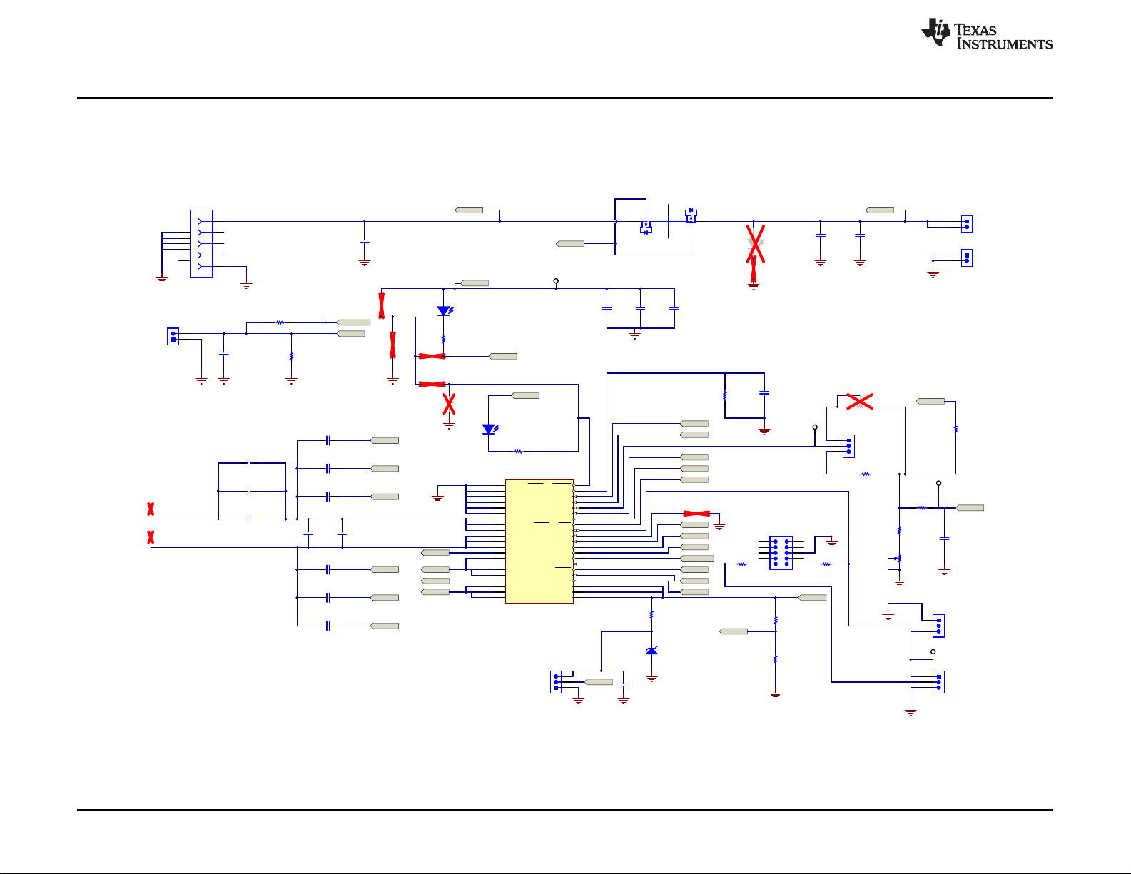
1 bq51020EVM-520 Schematic .............................................................................................. 4
2 bq51020 in Steady State Operation with bq24250 .................................................................... 11
3 Load Step ................................................................................................................... 12
4 Start Up With 500 mA ..................................................................................................... 13
5 System Efficiency Versus Output Power ............................................................................... 13
SLUUB03–April 2014 bq51020EVM (5-W WPC) Integrated Wireless Receiver Power Supply
Submit Documentation Feedback
Copyright © 2014, Texas Instruments Incorporated
1
Page 2

Introduction
6 Adapter Insertion and Removal .......................................................................................... 14
7 Thermal Image (1000-mA Load) ........................................................................................ 14
8 bq51020EVM-520 Layout Example ..................................................................................... 16
9 bq51020EVM-520 Top Assembly ....................................................................................... 17
10 bq51020EVM-520 Layer 1 ................................................................................................ 17
11 bq51020EVM-520 Layer 2 ................................................................................................ 18
12 bq51020EVM-520 Layer 3 ................................................................................................ 18
13 bq51020EVM-520 Layer 4 ................................................................................................ 19
1 bq51020EVM-520 Electrical Performance Specifications.............................................................. 3
2 Pin Description............................................................................................................... 6
3 bq51020EVM-520 Bill of Materials ...................................................................................... 20
1 Introduction
The bq51020 is an advanced, flexible, secondary-side device for wireless power transfer in portable
applications. The bq51020 device integrates an ultra-low-impedance synchronous rectifier, a very-highefficiency post regulator, digital control, and accurate voltage and current loops. The bq51020 devices
provide the AC/DC power conversion while integrating the digital control required. The IC complies with
the WPC v1.1 communication protocol.
Together with the bq500xxx primary-side controller transmitter, the bq51020 enables a complete
contactless power transfer system for a wireless power supply solution. By utilizing near-field inductive
power transfer, the secondary coil embedded in the mobile device can pick up the power transmitted by
the primary coil. The voltage from the secondary coil is then rectified and regulated to be used as a power
supply for down-system electronics. Global feedback is established from the secondary to the primary in
order to control the power transfer process.
A WPC system communication is digital -– packets are transferred from the secondary to the primary.
Differential bi-phase encoding is used for the packets. The bit rate is 2Kbps. Various types of
communication packets have been defined. These include identification and authentication packets, error
packets, control packets, power usage packets and efficiency packets, among others.
www.ti.com
List of Tables
2 Considerations with this EVM
The bq51020EVM-520 evaluation module (PWR520-002) demonstrates the receiver portion of the
wireless power system. This receiver EVM is a complete receiver-side solution that produces 5-W output
power at up to 1-A load with adjustable output voltage.
• The receiver can be used in any number of low-power battery portable devices as a power supply for a
battery charger. With contact-free charging capability, no connections to the device are needed.
• Highly-integrated wireless power receiver solution
– Ultra-efficient synchronous rectifier
– Very-high efficiency post regulator
– WPC v1.1-compliant communication and control
– Only one IC required between RX coil and DC output
• Programmable output voltage to optimize performance for application
• Adaptive Communication current limit (CM_ ILIM) for robust communication.
• Supports 20-V max input
• Low-power dissipative overvoltage clamp
• Overvoltage, overcurrent, overtemperature protection
• Low-profile, external pick-up coil
• Frame is configured to provide correct receiver to transmitter spacing
2
bq51020EVM (5-W WPC) Integrated Wireless Receiver Power Supply SLUUB03–April 2014
Copyright © 2014, Texas Instruments Incorporated
Submit Documentation Feedback
Page 3
www.ti.com
• Room above coil for testing with battery, key for Foreign Object Detection (FOD) tuning
• Options to adjust the input current limit and output voltage using resistors
• Flexibility for Foreign Object Detection (FOD) tuning
• Adjustable resistor that can be used to set RFOD
• Temperature sensing can be adjusted using external resistors
• Micro-USB connector for adapter testing configuration
• WPG LED indicator (turns on as V
OUT
• PD_DET LED indicator --turns on as the RX is on TX pad
3 Modifications
See the data sheet (SLUSBX1) when changing components. To aid in such customization of the EVM, the
board was designed with devices having 0402 and 0603 or larger footprints. A real implementation likely
occupies less total board space.
Note that changing components can improve or degrade EVM performance.
4 Recommended Operation Condition
Table 1 provides a summary of the bq51020EVM-520 performance specifications. All specifications are
given for an ambient temperature of 25°C.
Table 1. bq51020EVM-520 Electrical Performance Specifications
Modifications
goes high)
PARAMETER TEST CONDITION MIN TYP MAX UNIT
V
IN
I
AD_EN_sink
I
IN
I
OUT
V
OUT(REG)
f
s
T
J
(1)
The output voltage can be adjusted using V
operation of the EVM.
RECT input voltage range 4.0 10.0 V
Sink current 1 mA
Input current range 1.5 A
Output current range Current limit programming range 1.5 A
Programmable output voltage
Switching frequency WPC 110 205 kHz
Junction temperature 125 °C
(1)
P
= 5 W 4.5 8 V
OUT
resistors. Also the coil needs to change for different voltage for optimal
OUT(REG)
SLUUB03–April 2014 bq51020EVM (5-W WPC) Integrated Wireless Receiver Power Supply
Submit Documentation Feedback
Copyright © 2014, Texas Instruments Incorporated
3
Page 4
GND
1800pF
C4
0.068µF
C2
0.068µF
C1
BOOT1
RECTBOOT2
BOOT2
OUT
BOOT1
CLMP1
AD
FOD
VTSB/VIREG
CLMP2
COMM1
AD_EN
/WPG
COMM2
VO_REG
CM_ILIM
TS
CLMP1
0.47µF
C9
0.47µF
C12
CLMP2
COMM2
COMM1
GND
GND
VO_REG
1
2
J5
GND
0.1µF
C19
GND
TS
GND
VTSB/VIREG
TP1
DNP
TP2
DNP
2.00k
R13
DNP
GND
1.50k
R7
RECT
/WPG
GND
GND
0.1µF
C18
150
R2
FOD
TP5
1
2
3
JP1
110
R4
TP4
ADJ
TS
GND
ILIM
FIX
RECT
56.2k
R1
1
2
J3
1
2
J4
1
2
3
JP2
GND
CM_ILIM
High
Low
CM_ILIM
GND
GND
0.1µF
C16
TP3
GND
GND
0.1µF
C6
OUT
GNDGND
AD_EN
Rect
1µF
C17
GND
GND
GND
Out
ILIM
FOD
AC1
AC2
Orange
D2
Green
D1
1
2
3
4
5
6
7
8
9
10
11
J1
1 2
3 4
5 6
7 8
9 10
J2
GND
Q1
CSD75301W1015
OUT
AD
GND
20k
R15
10.0k
R11
5.11k
R16
0.047uF
C3
100pF
C5
10µF
C14
10µF
C15
1µF
C20
0
R3
OUT
0.015µF
C10
0.015µF
C11
0.022µF
C8
0.022µF
C13
3.3µF
C7
1.50k
R20
DNP
Green
D3
DNP
GND
102k
R17
DNP
102k
R14
11.3k
R18
DNP
11.3k
R10
102k
R19
DNP
5.6Meg
R12
27k
R21
DNP
100pF
C22
DNP
GND
PGND
A1
PGND
A2
PGND
A3
PGND
A4
PGND
A5
PGND
A6
AC1
B1
AC1
B2
AC1
B3
AC2
B4
AC2
B5
AC2
B6
BOOT1
C1
RECT
C2
RECT
C3
RECT
C4
RECT
C5
BOOT2
C6
OUT
D1
OUT
D2
OUT
D3
OUT
D4
OUT
D5
OUT
D6
CLAMP1
E1
AD
E2
AD_EN
E3
EN1/SCL
E4
VIREG
E5
CLAMP2
E6
COMM1
F1
FOD
F2
LPRBEN and TERM
F3
EN2/SDA
F4
LPRB1 and WPG
F5
COMM2
F6
VO_REG
G1
ILIM
G2
CM_ILIM
G3
TS
G4
TMEM
G5
LPRB2 and PD_DET
G6
U1
bq51020
2.2µF
C21
200
R9
200
R8
5 K
R5
DNP
500 Ohm
R6
1
2
3
JP3
1
2
3
JP4
TP6
Ext
GND
GND
Hi
Low
Hi
Low
EN1
EN2
102k
R22
5.1V
D4
BZT52C5V1T-7
GND
Equipment and EVM Setup
5 Equipment and EVM Setup
5.1 Schematic
Figure 1 shows the bq51020 schematic.
www.ti.com
Submit Documentation Feedback
Figure 1. bq51020EVM-520 Schematic
Copyright © 2014, Texas Instruments Incorporated
4
bq51020EVM (5-W WPC) Integrated Wireless Receiver Power Supply SLUUB03–April 2014
Page 5

www.ti.com
5.2 Connector Descriptions
The connections points are described in the following paragraphs.
5.2.1 J1 – AD External Adapter Input
Power can be provided to simulate an external adapter applied to the receiver in this bq51020EVM-520
(PWR520-002).
5.2.2 J2 – Programming Connector
This connector is populated and is for factory use only
5.2.3 J3 – Output Voltage
Output voltage in wireless power mode up to 1 A; the adapter option is also supported in this PWR520-
002.
5.2.4 J4 –GND
Ground return
5.2.5 J5 – TS/CTRL and Return Connector
External connection for temperature sense resistor, see data sheet for additional information. Not
populated in this spin.
Equipment and EVM Setup
5.3 Jumpers and Switches
The control jumpers are described in the following paragraphs.
5.3.1 JP1– ILIM (FIX or ADJ)
Maximum output current is set by the ILIM pin. In the FIX position, the current is set to a fixed value of R4
plus RFOD. In the ADJ position, current is set by R5. Note that R5 is not populated in this EVM.
5.3.2 JP2 – CM_ILIM
Enables CM_ILIM feature when pulled low and disable when pulled up.
5.3.3 JP3 – EN1 (Low and High)
EN1 pin, set High using external power supply connected to TP6 .
5.3.4 JP4 – EN2 (Low and High)
EN2 pin, set High using external power supply connected to TP6.
5.4 Test Point Descriptions
The test points are described in the following paragraphs.
5.4.1 TP1 and TP2 – AC1 and AC2 Inputs
This are not populated, they can be used for measuring AC voltage applied to the EVM from the receiver
coil.
5.4.2 TP3– Rectified Voltage
The input AC voltage is rectified into unregulated DC voltage (V
); additional capacitance is used to
RECT
filter the voltage before the regulator.
SLUUB03–April 2014 bq51020EVM (5-W WPC) Integrated Wireless Receiver Power Supply
Submit Documentation Feedback
Copyright © 2014, Texas Instruments Incorporated
5
Page 6

Equipment and EVM Setup
5.4.3 TP4– ILIM
Programming pin for overcurrent limit protection, pin G2 of the IC.
5.4.4 TP5 – FOD
Input for rectified power measurement for FOD feature in WPC, pin F2 of the IC. TP5 is the FOD pin for
the bq51020.
5.4.5 TP6 – Ext
Connect to 5-V external power supply. Used to pull EN1 and EN2 high. Any voltage level above 7 V may
damage the IC.
5.5 Pin Description of the IC
A1, A2, A3, A4, A5, A6 PGND
D1, D2, D3, D4, D5, D6 OUT
www.ti.com
Table 2. Pin Description
PIN Number (WCSP) bq51020
B1, B2, B3 AC1
B4, B5, B6 AC2
C1 BOOT1
C2, C3, C4, C5 RECT
C6 BOOT2
E1 CLAMP1
E2 AD
E3 AD_EN
E4 EN1
E5 VTSB
E6 CLAMP2
F1 COMM1
F2 FOD
F3 TERM
F4 EN2
F5 WPG
F6 COMM2
G1 VO_REG
G2 ILIM
G3 CM_ILIM
G4 TS/CTRL
G5 TMEM
G6 PD_DET
6 Test Procedure
This procedure describes test configuration of the bq51020EVM-520 evaluation board (PWR520-002) for
bench evaluation.
6.1 Definition
The following naming conventions are followed.
6
bq51020EVM (5-W WPC) Integrated Wireless Receiver Power Supply SLUUB03–April 2014
Copyright © 2014, Texas Instruments Incorporated
Submit Documentation Feedback
Page 7

www.ti.com
Test Procedure
VXXX : External voltage supply name (VADP, VTS, V
LOADW: External load name (LOADR, LOADI)
V(TPyy): Voltage at internal test point TPyy. For example, V(TP02) means the voltage at TP02.
V(Jxx): Voltage at header Jxx
V(TP(XXX)): Voltage at test point XXX. For example, V(ACDET) means the voltage at the test
point which is marked as ACDET.
V(XXX, YYY): Voltage across point XXX and YYY.
I(JXX(YYY)): Current going out from the YYY terminal of header XX.
Jxx(BBB): Terminal or pin BBB of header xx.
JPx ON : Internal jumper Jxx terminals are shorted.
JPx OFF: Internal jumper Jxx terminals are open.
JPx (-YY-) ON: Internal jumper Jxx adjacent terminals marked as YY are shorted.
Assembly drawings have locations for jumpers, test points, and individual components.
6.2 Recommended Test Equipment
The following equipment is needed to complete this test procedure:
Power Supplies
• Power Supply #1 (PS #1) capable of supplying 19 V at 1 A is required
• Power Supply #2 (PS #2) capable of supplying 5 V at 1 A is required
• Power Supply #3 (PS #3) capable of supplying 5 V at 1 A is required
Loads
• A resistive load or electronic load that can be set to 5 Ω/1000 mA, 10 Ω/500 mA, and 5 kΩ/1 mA. The
power rating should be 5 W.
Meters
• Two DC voltmeters and two DC ammeters
Oscilloscopes
• Not required
bqTesla Transmitter
• The HPA689 transmitter or equivalent is used for the final test.
Recommended Wire Gauge
• For proper operation, TI recommends 22-AWG wire.
OUT
)
6.3 Equipment Setup
The following items ensure proper equipment setup:
Test Set Up
• The final assembly will be tested using a bqTesla transmitter – provided (HPA689). Input voltage to the
transmitter is set to 19 VDC ±200 mV, with a current limit of 1.0 A.
• Connect power supply to J1 and J2 of the transmitter, HPA689
• Set power supply to OFF
• Place unit under test (UUT) on the transmitter coil
• UUT will be placed in the center of the HPA689 TX coil. Other bqTesla transmitter base units are also
acceptable for this test (ensure the correct input voltage is applied).
Load
• The load is connected between J3-OUT and J4-GND of the UUT
SLUUB03–April 2014 bq51020EVM (5-W WPC) Integrated Wireless Receiver Power Supply
Submit Documentation Feedback
Copyright © 2014, Texas Instruments Incorporated
7
Page 8

Test Procedure
• A DC ammeter is connected between UUT and load
• Set the load for 5 Ω/1000 mA
Jumper Settings
• JP1 → ILIM and FIX are shorted
• JP2 → CM_ILM and High are shorted
• JP3 → EN1 and Low are shorted
• JP4 → EN2 and Low are shorted
Voltage and Current Meters
• Connect the ammeter to measure 19-V input current to the transmitter. Connect the voltmeter to
monitor the input voltage at J1 and J2 of TX unit. On UUT a voltmeter is used to measure output
voltage at J3 with ground at J4. Connect the ammeter to measure load current.
RFOD: R6 Set Up
• Connect the ohmmeter between JP5 (FOD) and J4 (GND). Adjust R6 to a 495 Ω reading on the
ohmmeter.
• NOTE: Sometimes the multimeter cannot read the more than 430 Ω from the FOD resistor due to
charged up capacitors in the board. If that happens, use a twizer and short C15 for few seconds, then
measure again.
6.4 Procedure
The following operating procedures are provided at a variety of operating loads:
Turn ON Operation and Operation at 1000-mA Load
• Turn ON transmitter power supply (19 V)
• Transmitter – Verify LED D2 is ON
• UUT – Adjust load current to 1000 mA ±50 mA
• Put the receiver EVM on the transmitter coil and align them correctly
• After 5 seconds verify that:
– Transmitter – Status LED D5 should be green, flashing approximately every 1 second
– The transmitter should beep
– Transmitter – LED D2 still ON
– Receiver – LED D1 is ON
– UUT – Verify that V
– UUT – Verify that the rectified voltage is 5 V to 5.4 V (between TP3 and GND) NOTE: a modulation
signal is present on this voltage every 250 ms and may cause fluctuation in the reading: use lower
value or baseline.
Efficiency Test (1000-mA Load)
• Verify that input current to the TX is less than 500 mA with input voltage at 19 VDC
• Turn OFF the transmitter power supply (19 V)
Turn ON Operation and Operation at 500-mA Load
• Turn ON the transmitter power supply (19 V)
• Transmitter – Verify LED D2 is ON
• UUT – Adjust load current to 500 mA ±50 mA
• Put the receiver EVM on the transmitter coil and align them correctly
• After 5 seconds verify that:
– Transmitter – Status LED D5 should be green, flashing approximately every 1 second.
– The transmitter should beep
– Transmitter – LED D2 still ON
is 4.9 V to 5.15 V (between J3 and J4)
OUT
www.ti.com
8
bq51020EVM (5-W WPC) Integrated Wireless Receiver Power Supply SLUUB03–April 2014
Copyright © 2014, Texas Instruments Incorporated
Submit Documentation Feedback
Page 9

www.ti.com
Efficiency Test (500-mA Load)
• Verify that input current to the TX is less than 260 mA with an input voltage at 19 VDC
• Turn OFF the transmitter power supply (19 V)
Operation (1-mA Load)
• Turn ON the transmitter power supply (19 V)
• Transmitter – Verify LED D2 is ON
• UUT – Adjust load current to 1 mA ±200 µA
• Put the receiver EVM on the transmitter coil and align them correctly
• After 5 seconds verify that:
Efficiency Test (1-mA Load)
• Verify that input current to the TX is less than 80 mA with input voltage at 19 VDC
• Turn OFF the transmitter power supply (19 V)
• Remove UUT from transmitter
Adapter Test (500-mA Load)
• Connect 5 V ±250 mV adapter on J1 on the bq51020EVM-520 receiver
• Adjust the load current to 500 mA ±50 mA (J3 OUT and J4 GND)
• Verify that:
Test Procedure
– Receiver – LED D1 is ON
– UUT – Verify that V
is 4.9 V to 5.2 V (between J3 or TP7 and J4)
OUT
– UUT – Verify that the rectified voltage is 5 V to 5.4 V (between TP3 and GND) NOTE: a modulation
signal is present on this voltage every 250 ms and may cause fluctuation in the reading: use lower
value or baseline.
– Transmitter – Status LED D5 should be green, flashing approximately every 1 second.
– The transmitter should beep
– Transmitter – LED D2 still ON
– Receiver – LED D1 is ON
– UUT – Verify that V
is 4.9 V to 5.2 V (between J3 and J4)
OUT
– UUT – Verify that the rectified voltage is 6.9 V to 8.6 V (between TP3 and GND) NOTE: a
modulation signal is present on this voltage every 250 ms and may cause fluctuation in the reading:
use lower value or baseline.
1. UUT – LED D1 is OFF
2. UUT – V
is 5.0 V ±600 mV (J3)
OUT
3. Transmitter – Status LED D5 is OFF
4. Put external +5 V power supply to TP6 (Ext) and GND (J4)
5. Set the EN1 and EN2 jumper as follows:
• JP3: EN1 and Low are shorted
• JP4: EN2 and High are shorted
6. Put the receiver EVM on the transmitter coil and align them correctly while still having the adapter
connected to J1 and the external +5 V on TP6.
• After 5 seconds verify that:
– Transmitter – Status LED D5 should be green, flashing approximately every 1 second.
– The transmitter should beep
– Transmitter – LED D2 is still ON
– Receiver – LED D1 is ON
– UUT – Verify that V
is 4.9 V to 5.2 V (between J3 and J4)
OUT
– UUT – Verify that the rectified voltage is 5V to 5.6V (between TP3 and GND). NOTE: a
SLUUB03–April 2014 bq51020EVM (5-W WPC) Integrated Wireless Receiver Power Supply
Submit Documentation Feedback
Copyright © 2014, Texas Instruments Incorporated
9
Page 10

Test Procedure
7. Set the EN1 and EN2 jumper as follows:
8. Put the receiver EVM on the transmitter coil and align them correctly while still having the adapter
9. Verify that:
modulation signal is present on this voltage every 250 ms and may cause fluctuation in the
reading: use lower value or baseline.
– This disables wired power and prioritizes wireless power
• JP3: EN1 and High are shorted
• JP4: EN2 and High are shorted
connected to J1 and the external 5 V on TP6.
• UUT – LED D1 is OFF
• UUT – V
is 0 V ±600 mV (J3)
OUT
• Transmitter – Status LED D5 is ON
• This means both wired and wireless power are disabled
www.ti.com
10
bq51020EVM (5-W WPC) Integrated Wireless Receiver Power Supply SLUUB03–April 2014
Copyright © 2014, Texas Instruments Incorporated
Submit Documentation Feedback
Page 11

www.ti.com
7 Test Results
7.1 Steady-State Operation with bq2425x Charger
With the power supply off, connect the supply to the bqTESLA transmitter.
• Set up the test bench as described in Section 6.
• Power TX with 19 V.
• Connect the output of RX to a battery charger (bq24250) to charge a battery.
• Set the VBAT to 3.8 V.
• Set the charger current to 1.2 A.
• Set input current limit on the charger to 1 A.
• Monitor the I
them correctly.
• Figure 2 shows the V
OUT
and V
from the RX after putting the receiver EVM on the transmitter coil and align
OUT
OUT
and I
from the RX as the battery charges.
OUT
Test Results
Figure 2. bq51020 in Steady State Operation with bq24250
SLUUB03–April 2014 bq51020EVM (5-W WPC) Integrated Wireless Receiver Power Supply
Submit Documentation Feedback
Copyright © 2014, Texas Instruments Incorporated
11
Page 12

Test Results
7.2 Load Step
The procedure for load step is as follows:
• Set up the test bench as described in Section 6.
• Power WPC TX (bq500210) with 19 V.
• Provide a load step from no-load (high impedance) to 1000 mA (if using current source load).
• Monitor on side RX: load current, rectifier voltage, and output voltage as shown in Figure 3.
www.ti.com
7.3 Start Up
The procedure for start-up test with load:
• Set up the test bench as described in Section 6.
• Power the WPC TX
• Apply 10 Ω across J3 and J4, put the receiver EVM on the transmitter coil, and align them correctly
• Monitor the RECT pin, I
Figure 3. Load Step
, and output voltage, as shown in Figure 4.
OUT
12
bq51020EVM (5-W WPC) Integrated Wireless Receiver Power Supply SLUUB03–April 2014
Copyright © 2014, Texas Instruments Incorporated
Submit Documentation Feedback
Page 13

20
30
40
50
60
70
80
90
100
0 1000 2000 3000 4000 5000
Efficiency (%)
Power (mW)
TX-bq500211A
TX-bq500212A
C001
www.ti.com
Test Results
Figure 4. Start Up With 500 mA
7.4 Efficiency Data
7.4.1 Efficiency Versus Output Power (AC-DC)
Figure 5 illustrates the system (DC-DC) efficiency of the bq51020EVM-520 under different transmitters.
Figure 5. System Efficiency Versus Output Power
7.5 AD Insertion and Removal
Figure 6 illustrates the behavior of the bq51020EVM-520 when the AD is inserted while the EVM is on the
transmitter pad. There is some off time during the transition between wireless power and wired power
modes.
SLUUB03–April 2014 bq51020EVM (5-W WPC) Integrated Wireless Receiver Power Supply
Submit Documentation Feedback
Copyright © 2014, Texas Instruments Incorporated
13
Page 14

Test Results
www.ti.com
Figure 6. Adapter Insertion and Removal
7.6 Thermal Performance
This section shows a thermal image of the bq51020EVM-520. A 1-A load is used and the output voltage is
set to 5 V. There is no air flow and the ambient temperature is 25°C. The peak temperature of the device
(39°C in WPC) is well below the maximum recommended operating condition listed in the data sheet.
Figure 7. Thermal Image (1000-mA Load)
14
bq51020EVM (5-W WPC) Integrated Wireless Receiver Power Supply SLUUB03–April 2014
Copyright © 2014, Texas Instruments Incorporated
Submit Documentation Feedback
Page 15

www.ti.com
8 Layout and Bill of Material
8.1 bq51020 Traces
The bq51020 device pins can be classified as follows:
• Signal/Sensing Traces
– TS/CTRL, EN1, EN2, PD_DET, WPG, COMM, ILIM, AD, ADEN, FOD, TMEM, CM_ILIM, VO_REG,
VTSB, Term.
– Make sure these traces are not interfered by the noisy traces
• Noisy Traces
– AC1, AC2, BOOT, COMM
– Make sure these traces are isolated from other traces, use ground plan
• Power Traces
– AC1, AC2, OUT, CLAMP, PGND
– Make sure to use the correct width for the right current rating.
8.2 Layout Guidelines
Use the following layout guidelines:
• The traces from the input connector to the inputs of the bq51020 IC pin should be as wide as possible
to minimize the impedance in the lines. Otherwise, this causes a voltage drop and thermal issue.
• Keep the trace resistance as low as possible on AC1, AC2, OUT, and PGND.
• Use the appropriate current rating traces (width) the AC, OUT and PGND.
• The PCB should have a ground plane (return) connected directly to the return of all components
through vias (At least two vias per capacitor for power-stage capacitors, one via per capacitor for
small-signal components).
• The dissipation of heat path is important. Adding internal layers increases the thermal performance.
Multiple vias in the PGND pins of the IC is recommended to decrease the thermal resistance in the
board and allow much easier thermal dissipation through inner layer and power ground layers.
• The via interconnect is important and must be optimized near the power pad of the IC and the GND.
• 2-oz copper, or greater, is recommended
• For high-current applications, the balls for the power paths should be connected to as much copper in
the board as possible. This allows better thermal performance because the board conducts heat away
from the IC.
• It is always good practice to place high frequency bypass capacitors next to RECT and OUT.
Layout and Bill of Material
8.3 Printed-Circuit Board Layout Example
The primary concerns when laying a custom receiver PCB are as follows:
• AC1 and AC2, GND return trace resistance
• OUT trace resistance
• GND connection
• Copper weight ≥ 2 oz
For a 1-A fast charge current application, the current rating for each net is as follows:
• AC1 = AC2 = 1.2 A
• BOOT1 = BOOT2 = 1 A
• RECT = 50 mA
• OUT = 1 A
• COMM1 = COMM2 = 300 mA
• CLAMP1 = CLAMP2 = 500 mA
SLUUB03–April 2014 bq51020EVM (5-W WPC) Integrated Wireless Receiver Power Supply
Submit Documentation Feedback
Copyright © 2014, Texas Instruments Incorporated
15
Page 16

Layout and Bill of Material
• ILIM = 10 mA
• AD = AD_EN = TS/CTRL = EN1 = EN2 = TERM = FOD = 1 mA
• PWR = 10 mA
TI also recommends having the following capacitance on RECT and OUT:
• RECT ≥ 10 μF
• OUT ≥ 1 μF
It is always good practice to place high-frequency bypass capacitors next to RECT and OUT of 0.1 μF.
Figure 8 illustrates an example of a WCSP layout:
www.ti.com
16
Figure 8. bq51020EVM-520 Layout Example
bq51020EVM (5-W WPC) Integrated Wireless Receiver Power Supply SLUUB03–April 2014
Copyright © 2014, Texas Instruments Incorporated
Submit Documentation Feedback
Page 17

www.ti.com
8.4 bq51020EVM-520 Layout
Figure 9 through Figure 13 show the bq51020EVM-520 PCB layout.
Layout and Bill of Material
Figure 9. bq51020EVM-520 Top Assembly
Figure 10. bq51020EVM-520 Layer 1
SLUUB03–April 2014 bq51020EVM (5-W WPC) Integrated Wireless Receiver Power Supply
Submit Documentation Feedback
Copyright © 2014, Texas Instruments Incorporated
17
Page 18

Layout and Bill of Material
www.ti.com
Figure 11. bq51020EVM-520 Layer 2
18
Figure 12. bq51020EVM-520 Layer 3
bq51020EVM (5-W WPC) Integrated Wireless Receiver Power Supply SLUUB03–April 2014
Copyright © 2014, Texas Instruments Incorporated
Submit Documentation Feedback
Page 19

www.ti.com
Layout and Bill of Material
Figure 13. bq51020EVM-520 Layer 4
SLUUB03–April 2014 bq51020EVM (5-W WPC) Integrated Wireless Receiver Power Supply
Submit Documentation Feedback
Copyright © 2014, Texas Instruments Incorporated
19
Page 20

Layout and Bill of Material
www.ti.com
8.5 Bill of Materials (BOM)
Table 3 lists the BOM for the EVM.
Table 3. bq51020EVM-520 Bill of Materials
Designator Qty Value Description Package Part Number Manufacturer
!PCB 1 Printed Circuit Board PWR520 Any
C1, C2 2 0.068µF CAP CER 0.068UF 50V 10% X7R 0603 0603 GRM188R71H683KA93D MuRata
C3 1 0.047uF CAP CER 0.047UF 50V 10% X7R 0603 0603 GRM188R71H473KA61D MuRata
C4 1 1800pF CAP CER 1800PF 50V 10% X7R 0603 0603 GRM188R71H182KA01D MuRata
C5 1 100pF CAP, CERM, 100pF, 50V, +/-10%, X7R, 0402 0402 CC0402KRX7R9BB101 Yageo America
C6 1 0.1uF CAP, CERM, 0.1uF, 50V, +/-10%, X7R, 0402 0402 C1005X7R1H104K050BB TDK
C7 1 3.3uF CAP, CERM, 3.3uF, 25V, +/-10%, X5R, 0603 0603 C1608X5R1E335K080AC TDK
C8, C13 2 0.022uF CAP CER 0.022UF 25V 10% X7R 0603 0603 C0603C223K3RACTU Kemet
C9, C12 2 0.47uF CAP, CERM, 0.47uF, 25V, +/-10%, X5R, 0603 0603 GRM188R61E474KA12D MuRata
C10, C11 2 0.015uF CAP, CERM, 0.015uF, 50V, +/-10%, X7R, 0402 0402 GRM155R71H153KA12D MuRata
C14, C15 2 10uF CAP, CERM, 10uF, 25V, +/-10%, X5R, 0805 0805 C2012X5R1E106K125AB TDK
C16, C19 2 0.1uF CAP, CERM, 0.1uF, 50V, +/-10%, X7R, 0603 0603 GCM188R71H104KA57B MuRata
C17 1 1uF CAP, CERM, 1uF, 50V, +/-10%, X7R, 0805 0805 GRM21BR71H105KA12L MuRata
C18 1 0.1uF CAP, CERM, 0.1uF, 16V, +/-10%, X7R, 0402 0402 GRM155R71C104KA88D MuRata
C20 1 1uF CAP, CERM, 1uF, 25V, +/-10%, X7R, 0603 0603 GRM188R71E105KA12D MuRata
C21 1 2.2uF CAP, CERM, 2.2uF, 16V, +/-10%, X5R, 0603 0603 GRM188R61C225KE15D MuRata
D1 1 Green LED, Green, SMD 1.6x0.8x0.8mm LTST-C190GKT Lite-On
D2 1 Orange LED, Orange, SMD 1.6x0.8x0.8mm LTST-C190KFKT Lite-On
D4 1 5.1V Diode, Zener, 5.1V, 300mW, SOD-523 SOD-523 BZT52C5V1T-7 Diodes Inc.
H1 1 Tape segment, Low Static Polyimide Film. Cut tape section from 36 yard roll 1.5" x 2.3" 5419-1 1/2" 3M
H2 1 Case Modified Polycase LP-11B with 4 screws J-6838A Polycase
H3 1 Coil, RX with Attractor IWAS4832FFEB9R7J50 Vishay
H4, H5, H6, H7 4 #4 x 3/8" pan head phillips screw #4 x 3/8" PSMS 004 0038 PH BandFFastener
H8, H9, H10, H11 4 Spacer, 0.100" Thk x 0.25" OD x 0.147" ID 0.1" THK 905-100 Bivar
J1 1 Receptacle, Micro-USB-B, Right Angle, SMD Micro USB receptacle 105017-0001 Molex
J2 1 Connector, 100mil Shrouded, High-Temperature, Gold, TH 5x2 Shrouded header N2510-6002-RB 3M
J3, J4, J5 3 Header, 100mil, 2x1, Tin plated, TH Header, 2 PIN, 100mil, PEC02SAAN Sullins Connector
JP1, JP2, JP3, JP4 4 Header, 100mil, 3x1, Tin plated, TH Header, 3 PIN, 100mil, PEC03SAAN Sullins Connector
LBL1, LBL2 2 Thermal Transfer Printable Labels, 0.650" W x 0.200" H - 10,000 per roll PCB Label 0.650"H x THT-14-423-10 Brady
Q1 1 -20V MOSFET, P-CH, -20V, -1.2A, 2x3 DSBGA 2x3 DSBGA CSD75301W1015 Texas Instruments
R1 1 56.2k RES, 56.2k ohm, 1%, 0.063W, 0402 0402 CRCW040256K2FKED Vishay-Dale
R2 1 150 RES, 150 ohm, 5%, 0.063W, 0402 0402 CRCW0402150RJNED Vishay-Dale
R3 1 0 RES, 0 ohm, 5%, 0.063W, 0402 0402 CRCW04020000Z0ED Vishay-Dale
R4 1 110 RES, 110 ohm, 1%, 0.063W, 0402 0402 CRCW0402110RFKED Vishay-Dale
Reference
Tin Solutions
Tin Solutions
0.200"W
20
bq51020EVM (5-W WPC) Integrated Wireless Receiver Power Supply SLUUB03–April 2014
Submit Documentation Feedback
Copyright © 2014, Texas Instruments Incorporated
Page 21

www.ti.com
Layout and Bill of Material
Table 3. bq51020EVM-520 Bill of Materials (continued)
Designator Qty Value Description Package Part Number Manufacturer
R6 1 500 Ohm Trimmer, 500 ohm, 0.25W, TH 4.5x8x6.7mm 3266W-1-501LF Bourns
R7 1 1.50k RES, 1.50k ohm, 1%, 0.1W, 0603 0603 CRCW06031K50FKEA Vishay-Dale
R8, R9 2 200 RES, 200 ohm, 1%, 0.1W, 0603 0603 CRCW0603200RFKEA Vishay-Dale
R10 1 11.3k RES, 11.3k ohm, 1%, 0.05W, 0201 0201 ERJ-1GEF1132C Panasonic
R11 1 10.0k RES, 10.0k ohm, 1%, 0.063W, 0402 0402 CRCW040210K0FKED Vishay-Dale
R12 1 5.6Meg RES, 5.6Meg ohm, 5%, 0.05W, 0201 0201 MCR006YRTJ565 Rohm
R14 1 102k RES, 102k ohm, 1%, 0.05W, 0201 0201 ERJ-1GEF1023C Panasonic
R15 1 20k RES, 20k ohm, 5%, 0.063W, 0402 0402 CRCW040220K0JNED Vishay-Dale
R16 1 5.11k RES, 5.11k ohm, 1%, 0.1W, 0603 0603 CRCW06035K11FKEA Vishay-Dale
R22 1 102k RES, 102k ohm, 1%, 0.063W, 0402 0402 CRCW0402102KFKED Vishay-Dale
SH-JP1, SH-JP2, SH-JP3, SH- 4 1x2 Shunt, 100mil, Gold plated, Black Shunt 969102-0000-DA 3M
JP4
TP3, TP4, TP5 3 White Test Point, TH, Miniature, White Keystone5002 5002 Keystone
TP6 1 White Test Point, Miniature, White, TH White Miniature Testpoint 5002 Keystone
U1 1 WPC MODE (Qi) INTEGRATED WIRELESS RECEIVER POWER SUPPLY, YFP0042AWCG YFP0042AWCG bq51020YFP Texas Instruments
C22 0 100pF CAP, CERM, 100pF, 50V, +/-10%, X7R, 0402 0402 CC0402KRX7R9BB101 Yageo America
D3 0 Green LED, Green, SMD 1.6x0.8x0.8mm LTST-C190GKT Lite-On
FID1, FID2, FID3 0 Fiducialmark. There is nothing to buy or mount. Fiducial N/A N/A
R5 0 5 K Trimmer, 5k ohm, 0.25W, TH 4.5x8x6.7mm 3266W-1-502LF Bourns
R13 0 2.00k RES, 2.00k ohm, 1%, 0.1W, 0603 0603 RC0603FR-072KL Yageo America
R17, R19 0 102k RES, 102k ohm, 1%, 0.05W, 0201 0201 ERJ-1GEF1023C Panasonic
R18 0 11.3k RES, 11.3k ohm, 1%, 0.05W, 0201 0201 ERJ-1GEF1132C Panasonic
R20 0 1.50k RES, 1.50k ohm, 1%, 0.1W, 0603 0603 CRCW06031K50FKEA Vishay-Dale
R21 0 27k RES, 27k ohm, 5%, 0.1W, 0603 0603 CRCW060327K0JNEA Vishay-Dale
TP1, TP2 0 Black Test Point, Miniature, Black, TH Black Miniature Testpoint 5001 Keystone
Reference
SLUUB03–April 2014 bq51020EVM (5-W WPC) Integrated Wireless Receiver Power Supply
Submit Documentation Feedback
Copyright © 2014, Texas Instruments Incorporated
21
Page 22

ADDITIONAL TERMS AND CONDITIONS, WARNINGS, RESTRICTIONS, AND DISCLAIMERS FOR
EVALUATION MODULES
Texas Instruments Incorporated (TI) markets, sells, and loans all evaluation boards, kits, and/or modules (EVMs) pursuant to, and user
expressly acknowledges, represents, and agrees, and takes sole responsibility and risk with respect to, the following:
1. User agrees and acknowledges that EVMs are intended to be handled and used for feasibility evaluation only in laboratory and/or
development environments. Notwithstanding the foregoing, in certain instances, TI makes certain EVMs available to users that do not
handle and use EVMs solely for feasibility evaluation only in laboratory and/or development environments, but may use EVMs in a
hobbyist environment. All EVMs made available to hobbyist users are FCC certified, as applicable. Hobbyist users acknowledge, agree,
and shall comply with all applicable terms, conditions, warnings, and restrictions in this document and are subject to the disclaimer and
indemnity provisions included in this document.
2. Unless otherwise indicated, EVMs are not finished products and not intended for consumer use. EVMs are intended solely for use by
technically qualified electronics experts who are familiar with the dangers and application risks associated with handling electrical
mechanical components, systems, and subsystems.
3. User agrees that EVMs shall not be used as, or incorporated into, all or any part of a finished product.
4. User agrees and acknowledges that certain EVMs may not be designed or manufactured by TI.
5. User must read the user's guide and all other documentation accompanying EVMs, including without limitation any warning or
restriction notices, prior to handling and/or using EVMs. Such notices contain important safety information related to, for example,
temperatures and voltages. For additional information on TI's environmental and/or safety programs, please visit www.ti.com/esh or
contact TI.
6. User assumes all responsibility, obligation, and any corresponding liability for proper and safe handling and use of EVMs.
7. Should any EVM not meet the specifications indicated in the user’s guide or other documentation accompanying such EVM, the EVM
may be returned to TI within 30 days from the date of delivery for a full refund. THE FOREGOING LIMITED WARRANTY IS THE
EXCLUSIVE WARRANTY MADE BY TI TO USER AND IS IN LIEU OF ALL OTHER WARRANTIES, EXPRESSED, IMPLIED, OR
STATUTORY, INCLUDING ANY WARRANTY OF MERCHANTABILITY OR FITNESS FOR ANY PARTICULAR PURPOSE. TI SHALL
NOT BE LIABLE TO USER FOR ANY INDIRECT, SPECIAL, INCIDENTAL, OR CONSEQUENTIAL DAMAGES RELATED TO THE
HANDLING OR USE OF ANY EVM.
8. No license is granted under any patent right or other intellectual property right of TI covering or relating to any machine, process, or
combination in which EVMs might be or are used. TI currently deals with a variety of customers, and therefore TI’s arrangement with
the user is not exclusive. TI assumes no liability for applications assistance, customer product design, software performance, or
infringement of patents or services with respect to the handling or use of EVMs.
9. User assumes sole responsibility to determine whether EVMs may be subject to any applicable federal, state, or local laws and
regulatory requirements (including but not limited to U.S. Food and Drug Administration regulations, if applicable) related to its handling
and use of EVMs and, if applicable, compliance in all respects with such laws and regulations.
10. User has sole responsibility to ensure the safety of any activities to be conducted by it and its employees, affiliates, contractors or
designees, with respect to handling and using EVMs. Further, user is responsible to ensure that any interfaces (electronic and/or
mechanical) between EVMs and any human body are designed with suitable isolation and means to safely limit accessible leakage
currents to minimize the risk of electrical shock hazard.
11. User shall employ reasonable safeguards to ensure that user’s use of EVMs will not result in any property damage, injury or death,
even if EVMs should fail to perform as described or expected.
12. User shall be solely responsible for proper disposal and recycling of EVMs consistent with all applicable federal, state, and local
requirements.
Certain Instructions. User shall operate EVMs within TI’s recommended specifications and environmental considerations per the user’s
guide, accompanying documentation, and any other applicable requirements. Exceeding the specified ratings (including but not limited to
input and output voltage, current, power, and environmental ranges) for EVMs may cause property damage, personal injury or death. If
there are questions concerning these ratings, user should contact a TI field representative prior to connecting interface electronics including
input power and intended loads. Any loads applied outside of the specified output range may result in unintended and/or inaccurate
operation and/or possible permanent damage to the EVM and/or interface electronics. Please consult the applicable EVM user's guide prior
to connecting any load to the EVM output. If there is uncertainty as to the load specification, please contact a TI field representative. During
normal operation, some circuit components may have case temperatures greater than 60°C as long as the input and output are maintained
at a normal ambient operating temperature. These components include but are not limited to linear regulators, switching transistors, pass
transistors, and current sense resistors which can be identified using EVMs’ schematics located in the applicable EVM user's guide. When
placing measurement probes near EVMs during normal operation, please be aware that EVMs may become very warm. As with all
electronic evaluation tools, only qualified personnel knowledgeable in electronic measurement and diagnostics normally found in
development environments should use EVMs.
Agreement to Defend, Indemnify and Hold Harmless. User agrees to defend, indemnify, and hold TI, its directors, officers, employees,
agents, representatives, affiliates, licensors and their representatives harmless from and against any and all claims, damages, losses,
expenses, costs and liabilities (collectively, "Claims") arising out of, or in connection with, any handling and/or use of EVMs. User’s
indemnity shall apply whether Claims arise under law of tort or contract or any other legal theory, and even if EVMs fail to perform as
described or expected.
Safety-Critical or Life-Critical Applications. If user intends to use EVMs in evaluations of safety critical applications (such as life support),
and a failure of a TI product considered for purchase by user for use in user’s product would reasonably be expected to cause severe
personal injury or death such as devices which are classified as FDA Class III or similar classification, then user must specifically notify TI
of such intent and enter into a separate Assurance and Indemnity Agreement.
Page 23

RADIO FREQUENCY REGULATORY COMPLIANCE INFORMATION FOR EVALUATION MODULES
Texas Instruments Incorporated (TI) evaluation boards, kits, and/or modules (EVMs) and/or accompanying hardware that is marketed, sold,
or loaned to users may or may not be subject to radio frequency regulations in specific countries.
General Statement for EVMs Not Including a Radio
For EVMs not including a radio and not subject to the U.S. Federal Communications Commission (FCC) or Industry Canada (IC)
regulations, TI intends EVMs to be used only for engineering development, demonstration, or evaluation purposes. EVMs are not finished
products typically fit for general consumer use. EVMs may nonetheless generate, use, or radiate radio frequency energy, but have not been
tested for compliance with the limits of computing devices pursuant to part 15 of FCC or the ICES-003 rules. Operation of such EVMs may
cause interference with radio communications, in which case the user at his own expense will be required to take whatever measures may
be required to correct this interference.
General Statement for EVMs including a radio
User Power/Frequency Use Obligations: For EVMs including a radio, the radio included in such EVMs is intended for development and/or
professional use only in legally allocated frequency and power limits. Any use of radio frequencies and/or power availability in such EVMs
and their development application(s) must comply with local laws governing radio spectrum allocation and power limits for such EVMs. It is
the user’s sole responsibility to only operate this radio in legally acceptable frequency space and within legally mandated power limitations.
Any exceptions to this are strictly prohibited and unauthorized by TI unless user has obtained appropriate experimental and/or development
licenses from local regulatory authorities, which is the sole responsibility of the user, including its acceptable authorization.
U.S. Federal Communications Commission Compliance
For EVMs Annotated as FCC – FEDERAL COMMUNICATIONS COMMISSION Part 15 Compliant
Caution
This device complies with part 15 of the FCC Rules. Operation is subject to the following two conditions: (1) This device may not cause
harmful interference, and (2) this device must accept any interference received, including interference that may cause undesired operation.
Changes or modifications could void the user's authority to operate the equipment.
FCC Interference Statement for Class A EVM devices
This equipment has been tested and found to comply with the limits for a Class A digital device, pursuant to part 15 of the FCC Rules.
These limits are designed to provide reasonable protection against harmful interference when the equipment is operated in a commercial
environment. This equipment generates, uses, and can radiate radio frequency energy and, if not installed and used in accordance with the
instruction manual, may cause harmful interference to radio communications. Operation of this equipment in a residential area is likely to
cause harmful interference in which case the user will be required to correct the interference at its own expense.
FCC Interference Statement for Class B EVM devices
This equipment has been tested and found to comply with the limits for a Class B digital device, pursuant to part 15 of the FCC Rules.
These limits are designed to provide reasonable protection against harmful interference in a residential installation. This equipment
generates, uses and can radiate radio frequency energy and, if not installed and used in accordance with the instructions, may cause
harmful interference to radio communications. However, there is no guarantee that interference will not occur in a particular installation. If
this equipment does cause harmful interference to radio or television reception, which can be determined by turning the equipment off and
on, the user is encouraged to try to correct the interference by one or more of the following measures:
• Reorient or relocate the receiving antenna.
• Increase the separation between the equipment and receiver.
• Connect the equipment into an outlet on a circuit different from that to which the receiver is connected.
• Consult the dealer or an experienced radio/TV technician for help.
Industry Canada Compliance (English)
For EVMs Annotated as IC – INDUSTRY CANADA Compliant:
This Class A or B digital apparatus complies with Canadian ICES-003.
Changes or modifications not expressly approved by the party responsible for compliance could void the user’s authority to operate the
equipment.
Concerning EVMs Including Radio Transmitters
This device complies with Industry Canada licence-exempt RSS standard(s). Operation is subject to the following two conditions: (1) this
device may not cause interference, and (2) this device must accept any interference, including interference that may cause undesired
operation of the device.
Concerning EVMs Including Detachable Antennas
Under Industry Canada regulations, this radio transmitter may only operate using an antenna of a type and maximum (or lesser) gain
approved for the transmitter by Industry Canada. To reduce potential radio interference to other users, the antenna type and its gain should
be so chosen that the equivalent isotropically radiated power (e.i.r.p.) is not more than that necessary for successful communication.
This radio transmitter has been approved by Industry Canada to operate with the antenna types listed in the user guide with the maximum
permissible gain and required antenna impedance for each antenna type indicated. Antenna types not included in this list, having a gain
greater than the maximum gain indicated for that type, are strictly prohibited for use with this device.
Page 24

Canada Industry Canada Compliance (French)
Cet appareil numérique de la classe A ou B est conforme à la norme NMB-003 du Canada
Les changements ou les modifications pas expressément approuvés par la partie responsable de la conformité ont pu vider l’autorité de
l'utilisateur pour actionner l'équipement.
Concernant les EVMs avec appareils radio
Le présent appareil est conforme aux CNR d'Industrie Canada applicables aux appareils radio exempts de licence. L'exploitation est
autorisée aux deux conditions suivantes : (1) l'appareil ne doit pas produire de brouillage, et (2) l'utilisateur de l'appareil doit accepter tout
brouillage radioélectrique subi, même si le brouillage est susceptible d'en compromettre le fonctionnement.
Concernant les EVMs avec antennes détachables
Conformément à la réglementation d'Industrie Canada, le présent émetteur radio peut fonctionner avec une antenne d'un type et d'un gain
maximal (ou inférieur) approuvé pour l'émetteur par Industrie Canada. Dans le but de réduire les risques de brouillage radioélectrique à
l'intention des autres utilisateurs, il faut choisir le type d'antenne et son gain de sorte que la puissance isotrope rayonnée équivalente
(p.i.r.e.) ne dépasse pas l'intensité nécessaire à l'établissement d'une communication satisfaisante.
Le présent émetteur radio a été approuvé par Industrie Canada pour fonctionner avec les types d'antenne énumérés dans le manuel
d’usage et ayant un gain admissible maximal et l'impédance requise pour chaque type d'antenne. Les types d'antenne non inclus dans
cette liste, ou dont le gain est supérieur au gain maximal indiqué, sont strictement interdits pour l'exploitation de l'émetteur.
Mailing Address: Texas Instruments, Post Office Box 655303, Dallas, Texas 75265
Copyright © 2014, Texas Instruments Incorporated
spacer
Important Notice for Users of EVMs Considered “Radio Frequency Products” in Japan
EVMs entering Japan are NOT certified by TI as conforming to Technical Regulations of Radio Law of Japan.
If user uses EVMs in Japan, user is required by Radio Law of Japan to follow the instructions below with respect to EVMs:
1. Use EVMs in a shielded room or any other test facility as defined in the notification #173 issued by Ministry of Internal Affairs and
Communications on March 28, 2006, based on Sub-section 1.1 of Article 6 of the Ministry’s Rule for Enforcement of Radio Law of
Japan,
2. Use EVMs only after user obtains the license of Test Radio Station as provided in Radio Law of Japan with respect to EVMs, or
3. Use of EVMs only after user obtains the Technical Regulations Conformity Certification as provided in Radio Law of Japan with respect
to EVMs. Also, do not transfer EVMs, unless user gives the same notice above to the transferee. Please note that if user does not
follow the instructions above, user will be subject to penalties of Radio Law of Japan.
http://www.tij.co.jp
【無線電波を送信する製品の開発キットをお使いになる際の注意事項】 本開発キットは技術基準適合証明を受けておりません。 本製品の
ご使用に際しては、電波法遵守のため、以下のいずれかの措置を取っていただく必要がありますのでご注意ください。
1. 電波法施行規則第6条第1項第1号に基づく平成18年3月28日総務省告示第173号で定められた電波暗室等の試験設備でご使用いただく。
2. 実験局の免許を取得後ご使用いただく。
3. 技術基準適合証明を取得後ご使用いただく。。
なお、本製品は、上記の「ご使用にあたっての注意」を譲渡先、移転先に通知しない限り、譲渡、移転できないものとします
上記を遵守頂けない場合は、電波法の罰則が適用される可能性があることをご留意ください。
日本テキサス・インスツルメンツ株式会社
東京都新宿区西新宿6丁目24番1号
西新宿三井ビル
http://www.tij.co.jp
Texas Instruments Japan Limited
(address) 24-1, Nishi-Shinjuku 6 chome, Shinjuku-ku, Tokyo, Japan
Page 25

IMPORTANT NOTICE
Texas Instruments Incorporated and its subsidiaries (TI) reserve the right to make corrections, enhancements, improvements and other
changes to its semiconductor products and services per JESD46, latest issue, and to discontinue any product or service per JESD48, latest
issue. Buyers should obtain the latest relevant information before placing orders and should verify that such information is current and
complete. All semiconductor products (also referred to herein as “components”) are sold subject to TI’s terms and conditions of sale
supplied at the time of order acknowledgment.
TI warrants performance of its components to the specifications applicable at the time of sale, in accordance with the warranty in TI’s terms
and conditions of sale of semiconductor products. Testing and other quality control techniques are used to the extent TI deems necessary
to support this warranty. Except where mandated by applicable law, testing of all parameters of each component is not necessarily
performed.
TI assumes no liability for applications assistance or the design of Buyers’ products. Buyers are responsible for their products and
applications using TI components. To minimize the risks associated with Buyers’ products and applications, Buyers should provide
adequate design and operating safeguards.
TI does not warrant or represent that any license, either express or implied, is granted under any patent right, copyright, mask work right, or
other intellectual property right relating to any combination, machine, or process in which TI components or services are used. Information
published by TI regarding third-party products or services does not constitute a license to use such products or services or a warranty or
endorsement thereof. Use of such information may require a license from a third party under the patents or other intellectual property of the
third party, or a license from TI under the patents or other intellectual property of TI.
Reproduction of significant portions of TI information in TI data books or data sheets is permissible only if reproduction is without alteration
and is accompanied by all associated warranties, conditions, limitations, and notices. TI is not responsible or liable for such altered
documentation. Information of third parties may be subject to additional restrictions.
Resale of TI components or services with statements different from or beyond the parameters stated by TI for that component or service
voids all express and any implied warranties for the associated TI component or service and is an unfair and deceptive business practice.
TI is not responsible or liable for any such statements.
Buyer acknowledges and agrees that it is solely responsible for compliance with all legal, regulatory and safety-related requirements
concerning its products, and any use of TI components in its applications, notwithstanding any applications-related information or support
that may be provided by TI. Buyer represents and agrees that it has all the necessary expertise to create and implement safeguards which
anticipate dangerous consequences of failures, monitor failures and their consequences, lessen the likelihood of failures that might cause
harm and take appropriate remedial actions. Buyer will fully indemnify TI and its representatives against any damages arising out of the use
of any TI components in safety-critical applications.
In some cases, TI components may be promoted specifically to facilitate safety-related applications. With such components, TI’s goal is to
help enable customers to design and create their own end-product solutions that meet applicable functional safety standards and
requirements. Nonetheless, such components are subject to these terms.
No TI components are authorized for use in FDA Class III (or similar life-critical medical equipment) unless authorized officers of the parties
have executed a special agreement specifically governing such use.
Only those TI components which TI has specifically designated as military grade or “enhanced plastic” are designed and intended for use in
military/aerospace applications or environments. Buyer acknowledges and agrees that any military or aerospace use of TI components
which have not been so designated is solely at the Buyer's risk, and that Buyer is solely responsible for compliance with all legal and
regulatory requirements in connection with such use.
TI has specifically designated certain components as meeting ISO/TS16949 requirements, mainly for automotive use. In any case of use of
non-designated products, TI will not be responsible for any failure to meet ISO/TS16949.
Products Applications
Audio www.ti.com/audio Automotive and Transportation www.ti.com/automotive
Amplifiers amplifier.ti.com Communications and Telecom www.ti.com/communications
Data Converters dataconverter.ti.com Computers and Peripherals www.ti.com/computers
DLP® Products www.dlp.com Consumer Electronics www.ti.com/consumer-apps
DSP dsp.ti.com Energy and Lighting www.ti.com/energy
Clocks and Timers www.ti.com/clocks Industrial www.ti.com/industrial
Interface interface.ti.com Medical www.ti.com/medical
Logic logic.ti.com Security www.ti.com/security
Power Mgmt power.ti.com Space, Avionics and Defense www.ti.com/space-avionics-defense
Microcontrollers microcontroller.ti.com Video and Imaging www.ti.com/video
RFID www.ti-rfid.com
OMAP Applications Processors www.ti.com/omap TI E2E Community e2e.ti.com
Wireless Connectivity www.ti.com/wirelessconnectivity
Mailing Address: Texas Instruments, Post Office Box 655303, Dallas, Texas 75265
Copyright © 2014, Texas Instruments Incorporated
Page 26

Mouser Electronics
Authorized Distributor
Click to View Pricing, Inventory, Delivery & Lifecycle Information:
Texas Instruments:
BQ51020EVM-520
 Loading...