

Page 1

User's Guide
SLUU911–June 2012
bq51013AEVM-765 Evaluation Module
The bq51013AEVM-765 wireless power receiver evaluation kit from Texas Instruments is a highperformance, easy-to-use development kit for the design of wireless power solutions. Consisting of a 5-V
power supply receiver and associated magnetics, the kit enables designers to speed the development of
their end-applications.
Contents
1 Applications .................................................................................................................. 2
2 bq51013AEVM-765 Electrical Performance Specifications ........................................................... 2
3 Modifications ................................................................................................................. 2
4 Connector and Test Point Descriptions .................................................................................. 2
4.1 Input/Output Connections ......................................................................................... 2
4.2 Jumpers/Switches .................................................................................................. 3
4.3 Test Point Descriptions ............................................................................................ 3
5 Schematic and Bill of Materials ........................................................................................... 5
6 Test Setup ................................................................................................................... 6
6.1 Equipment ........................................................................................................... 6
6.2 Equipment Setup ................................................................................................... 7
6.3 Load Step ........................................................................................................... 8
6.4 Load Dump ......................................................................................................... 9
6.5 V-Adapter Input ..................................................................................................... 9
6.6 Start-Up ............................................................................................................ 10
6.7 Disable Shutdown ................................................................................................ 10
6.8 System Efficiency ................................................................................................. 11
6.9 Dynamic Rectifier Control / Dynamic Efficiency Scaling .................................................... 11
7 Layout Guidelines ......................................................................................................... 12
8 bq51013AEVM-765 Assembly Drawings and Layout ................................................................. 13
9 Reference ................................................................................................................... 16
List of Figures
1 HPA765AEVM Schematic ................................................................................................. 5
2 Equipment Setup............................................................................................................ 7
3 Load Step, 0 mA to 500 mA............................................................................................... 8
4 Load Dump, 500 mA to 0 mA ............................................................................................. 9
5 V-Adapter Input.............................................................................................................. 9
6 Start-Up..................................................................................................................... 10
7 Equipment Shutdown Wireless Disable ................................................................................ 10
8 bq51013AEVM-765 Efficiency vs Output Power ...................................................................... 11
9 bq51013AEVM-765 V-rect vs Output Power........................................................................... 11
10 QFN Layout ................................................................................................................ 12
11 Top Assembly.............................................................................................................. 13
12 Top Copper Layer......................................................................................................... 14
13 Bottom Copper Layer .................................................................................................... 15
14 Bottom Assembly.......................................................................................................... 16
bqTESLA is a trademark of Texas Instruments.
SLUU911–June 2012 bq51013AEVM-765 Evaluation Module
Submit Documentation Feedback
Copyright © 2012, Texas Instruments Incorporated
1
Page 2
Applications
List of Tables
1 bq51013AEVM-765 Electrical Performance Specifications ........................................................... 2
2 Bill of Materials.............................................................................................................. 6
1 Applications
The bq51013AEVM-765 evaluation module (EVM) demonstrates the receiver portion of the bqTESLA™
wireless power system. This receiver EVM is a complete receiver-side solution that produces 5 V out at up
to 1 A when coupled with the bqTESLA™ transmitter. The bq51013AEVM-765 device shown on this EVM
along with external components that support the device for a complete solution.
• The bqTESLA™ receiver can be used in any number of low-power battery portable devices as a power
source for charging. With contact-free charging capability, no connections to the device are needed.
• Output voltage of 5 V up to 1 A
• External adapter switchover and control circuit
• Low-profile, external pick-up coil
• Frame is configured to provide correct receiver to transmitter spacing.
• Room above coil for testing with battery, key for tuning
• Adjustable resistor R16 can be used to set max output current
2 bq51013AEVM-765 Electrical Performance Specifications
Table 1 provides a summary of the bq51013AEVM-765 performance specifications. All specifications are
given for an ambient temperature of 25°C.
www.ti.com
Table 1. bq51013AEVM-765 Electrical Performance Specifications
Parameter Notes and Conditions Min Typ Max Unit
INPUT CHARACTERISTICS
V
IN
V
ADAPTER
OVP
OUTPUT CHARACTERISTICS
V
OUT
I
OUT
SYSTEMS CHARACTERISTICS
F
S
Eff Efficiency Output current 500 mA 74 %
Input Voltage Typical V-rectified voltage at TP12 4 5.5 8 V
Adapter Input Voltage 4 7 20 V
Input Overvoltage Voltage at V-rectified 15 V
Protection
V J3 to J4 5 V
I J3 1 A
Switching Frequency 110 205 kHz
3 Modifications
See the data sheet (SLUSAY6) when changing components. To aid in such customization of the EVM, the
board was designed with devices having 0603 or larger footprints. A real implementation likely occupies
less total board space.
Note that changing components can improve or degrade EVM performance.
4 Connector and Test Point Descriptions
4.1 Input/Output Connections
The connections points are described in the following paragraphs.
2
bq51013AEVM-765 Evaluation Module SLUU911–June 2012
Copyright © 2012, Texas Instruments Incorporated
Submit Documentation Feedback
Page 3

www.ti.com
4.1.1 J1 – AD External Adapter Input, J2-GND
Power can be provided to simulate an external adapter applied to the receiver. When this is done, an End
Power Transfer signal is sent to the transmitter which enters a low power state. External adapter voltage
must be a minimum of 4 V but not exceed 20V.
4.1.2 J3 – Output Voltage, J4-GND
Output voltage is 5 V in wireless power mode up to 1 A or adapter voltage if adapter is used.
4.1.3 J5 – TS and Return Connector
External connection for Temperature Sense Resistor, see data sheet for additional info.
4.1.4 J6 – Programming Connector
This connector is only useful at factory level.
4.2 Jumpers/Switches
The control jumpers are described in the following paragraphs.
4.2.1 JP1 – EN1 Enable 1
One of two Enable signals that controls the Adapter and Wireless power transfer. Low on EN1 enables the
wireless power transfer; High disables the wireless power transfer. The Default Shorting jumper setting is
Low.
Connector and Test Point Descriptions
4.2.2 JP2 – EN2 Enable 2
One of two Enable signals that controls the Adapter and Wireless power transfer. Low on EN2 enables the
adapter power transfer also High disables Comm-I
4.2.3 JP3 – TS Enable or Disable
This jumper enables the TS adjustment feature using R3. The Disable position sets voltage at the TS pin
to a safe value. The Default Shorting jumper setting is disabled
4.2.4 JP4 – Pull-Up to Out or Vz
EN1 and EN2 pull-up along with LED D1 can be powered from OUT or RECT. Vz is derived from RECT
through a resistor and zener diode.
4.2.5 JP5 – CS100 TS Enable or Disable
Only used for bq51014 device. This jumper along with R14 and R13 will enable the Charge Status 100%
feature. See data sheet for additional info. Open will disable.
4.2.6 JP6 – ILIM Fix or ADJ
Max output current is set by I-lim pin. In the FIX position current is set to 1.2A max. In the ADJ position
current is set by R16.
4.3 Test Point Descriptions
The test points are described in the following paragraphs.
. Default Shorting jumper setting is Low.
ILIM
4.3.1 TP1 – AD_EN
This push-pull driver for the external PFET connects the Adapter and the Output from the bq51013.
SLUU911–June 2012 bq51013AEVM-765 Evaluation Module
Submit Documentation Feedback
Copyright © 2012, Texas Instruments Incorporated
3
Page 4

Connector and Test Point Descriptions
4.3.2 TP2 – AC Input 2
This is the test point for measuring ac voltage applied to the EVM from the receiver coil.
4.3.3 TP3 – Com2 Communication 2 Drive
Communication driver signal, open-drain output connected to communication capacitor.
4.3.4 TP4 – AC Input 1
This is the test point for measuring ac voltage applied to the EVM from the receiver coil.
4.3.5 TP5 – CLMP 1
Overvoltage clamp driver signal, open-drain output is connected to OVP capacitor.
4.3.6 TP6 – CLMP 2
Overvoltage clamp drive signal, open-drain output is connected to OVP capacitor.
4.3.7 TP7 – OUT Output Voltage
This test point is the output voltage from the bq51013 or the Adapter input.
4.3.8 TP8 – Boot-1 Boot Capacitor
This bootstrap capacitor 1 drive connects to the integrated circuit (IC).
www.ti.com
4.3.9 TP9 – Boot-2 Boot Capacitor
This bootstrap capacitor 2 drive connects to the IC.
4.3.10 TP10 – CHG Charge
This output signal indicates that the output current is being delivered to OUT, the open-drain output.
4.3.11 TP11 – AC1 IC input
This is the ac input to the IC from series capacitors.
4.3.12 TP12 – Rectified Voltage
The input ac voltage is rectified into unregulated dc voltage; additional capacitance is used to filter the
voltage before the regulator.
4.3.13 TP13, TP14, TP15 – GND
These are the ground test points.
4.3.14 TP16 – TS Temp Sensor
This is the connection point for external thermistor; see the data sheet for additional information.
4.3.15 TP17 – FOD
Input for rectified power measurment, pin 14 of the IC.
4.3.16 TP18– ILIM
Programming pin for over current limit, pin 12 of the IC.
4
bq51013AEVM-765 Evaluation Module SLUU911–June 2012
Copyright © 2012, Texas Instruments Incorporated
Submit Documentation Feedback
Page 5
1
1
1
1
1
www.ti.com
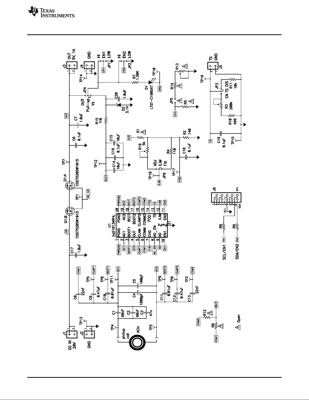
5 Schematic and Bill of Materials
Schematic and Bill of Materials
NOTE: For Reference Only, See Table 2 for Specific Values
Figure 1. HPA765AEVM Schematic
SLUU911–June 2012 bq51013AEVM-765 Evaluation Module
Submit Documentation Feedback
Copyright © 2012, Texas Instruments Incorporated
5
Page 6

Test Setup
www.ti.com
Table 2. Bill of Materials
COUNT RefDes Value DESCRIPTION SIZE Part Number MFR
1 U1 bq51013ARHL IC, bq51013A Wireless Power Receiver QFN-20 bq51013ARHL TI
1 Q1 CSD75205W1015 MOSFET, Dual PChan, -20V, 1.2A, CSP CSD75205W1015 TI
2 C1, C2 68nF Capacitor, Ceramic, 50V, X7R, 10% 0603 Std Std
1 C3 47nF Capacitor, Ceramic, 50V, X7R, 10% 0603 Std Std
1 C4 1800pF Capacitor, Ceramic, 50V, X7R, 10% 0603 Std Std
1 C5 100pF Capacitor, Ceramic, 50V, X7R, 10% 0603 Std Std
4 C6, C16, C18, 0.1uF Capacitor, Ceramic, 50V, X7R, 10% 0603 Std Std
C19
2 C7, C17 1.0uF Capacitor, Ceramic, 25V, X5R, 10% 0603 Std Std
2 C8, C13 22nF Capacitor, Ceramic, 50V, X7R, 10% 0603 Std Std
2 C9, C12 0.47uF Capacitor, Ceramic, 25V, X5R, 10% 0603 Std Std
2 C10, C11 0.01uF Capacitor, Ceramic, 50V, X7R, 10% 0603 Std Std
2 C14, C15 10uF Capacitor, Ceramic, 25V, X5R, 10% 1206 Std Std
1 C20 1.0uF Capacitor, Ceramic, 50V, X5R, 10% 0805 Std Std
1 D1 LTST-C190GKT Diode, LED, Green, 2.1-V, 20-mA, 6-mcd 0603 LTST-C190GKT LiteOn
1 D2 5.1V Diode, Zener, 5.1V, 300mW SOD-523 BZT52C5V1T Diodes, Inc.
0 R1, R5, R14 Open Resistor,Chip, 1/16W, 1% 0603 STD STD
1 R2 140 Resistor, Chip, 1/16W, 1% 0603 Std Std
1 R3 200k Potentiometer, 1/4 in. Cermet, 12-Turn, 0.25x0.17 3266W-1-204LF Bourns
1 R4 110 Resistor, Chip, 1/16W, 1% 0603 Std Std
0 R6, R12 Open Resistor, Metal Film, 1/4 watt, ± 1% 1206 CRCW120624R0FKEA Vishay
1 R7 1.50K Resistor, Chip, 1/16W, 1% 0603 Std Std
2 R8, R9 200 Resistor, Chip, 1/16W, 1% 0603 Std Std
1 R10 499 Resistor, Chip, 1/16W, 1% 0603 Std Std
1 R11 10.0k Resistor, Chip, 1/16W, 1% 0603 Std Std
1 R15 110K Resistor, Chip, 1/16W, 1% 0603 Std Std
0 R13 Open Potentiometer, 1/4 in. Cermet, 12-Turn, 0.25x0.17 3266W-1-203LF Bourns
1 R16 5k Potentiometer, 1/4 in. Cermet, 12-Turn, 0.25x0.17 3266W-1-502LF Bourns
1 Coil, RX with Attractor IWAS-4832FF-50 or Vishay or
190 milliOhm 1x1.5mm
Top-Adjust
Top-Adjust
Top-Adjust
WR-483250-15M2-G or TDK or
760308201 Wurth
6 Test Setup
6.1 Equipment
6.1.1 bqTESLA™ Transmitter
Power for the bq51013AEVM-765 receiver EVM is supplied through a bqTESLA™ transmitter
(bq500210EVM-689) or WPC-certified transmitter. The input ac voltage is applied to the receiver through
the coil located in the receiver bottom.
6.1.2 Voltage Source
Input power supply to the bqTESLA™ transmitter(bq500210EVM-689) is typically 19 Vdc ±200 mV at 500
mA maximum, but consult transmitter specification. To simulate an external adapter, an additional 5 V at
the 1-A power supply is used.
6
bq51013AEVM-765 Evaluation Module SLUU911–June 2012
Copyright © 2012, Texas Instruments Incorporated
Submit Documentation Feedback
Page 7
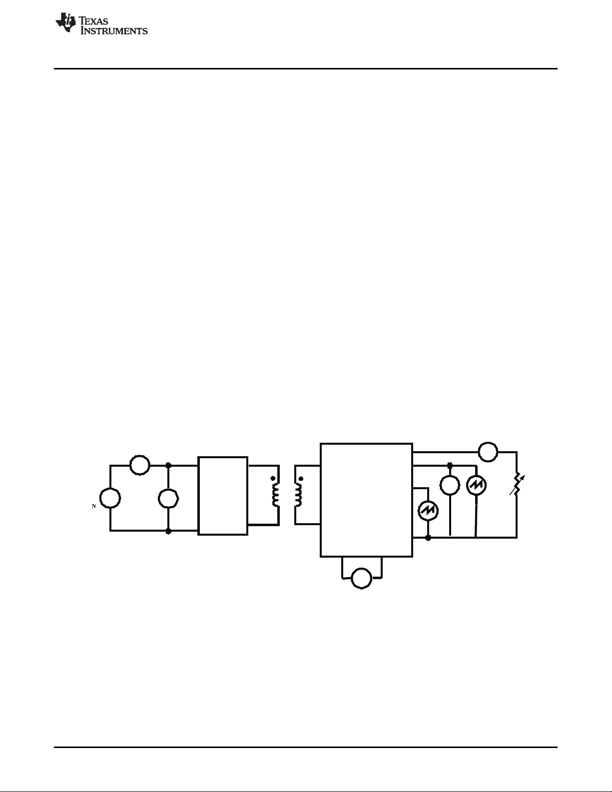
+
-
V
Wireless
Transmitter
V
A
A
R
L
L
P
L
S
AC1
OUT-J3
V
I
VRECT-TP12
AC2
GND-J4
OUT-TP7
Wireless Receiver
bq51013AEVM-765
+
-
GND-J2V-adapter-J1
www.ti.com
6.1.3 Meters
Output voltage can be monitored at TP7 with a voltmeter. Input current into the load must be monitored
with an appropriate ammeter. Transmitter input current and voltage can be monitored also but the meter
must use averaging function for reducing error due to communications packets.
6.1.4 Loads
A single load is required for 5 V with a maximum current of 1 A. The load can be resistive or electronic.
6.1.5 Oscilloscope
A multichannel oscilloscope with appropriate probes is used to observe the RECT voltage at TP12 and
other signals.
6.1.6 Recommended Wire Gauge
For proper operation, 22 AWG wire is recommended when connecting the bq51013AEVM-765EVM to
loads.
6.2 Equipment Setup
• With the power supply off, connect supply to the bqTESLA™ transmitter.
• Place the bqTESLA™ receiver on the transmitter.
• Connect load to J3 with return to J4, monitor current through load with ammeter, and monitor current to
load at TP7.
• Typical output voltage is 5 V, and the output current range is 0 mA to 1 A.
Test Setup
6.2.1 Equipment Setup Diagram
The diagram of Figure 2 shows the equipment test setup.
Figure 2. Equipment Setup
SLUU911–June 2012 bq51013AEVM-765 Evaluation Module
Submit Documentation Feedback
Copyright © 2012, Texas Instruments Incorporated
7
Page 8

V-RECT
TP7 5V-OUT
I-OUT
Test Setup
6.2.2 EVM Setup Procedures
This section guides the user through a few general test procedures to exercise the functionality of the
presented hardware. A few key notes:
• To probe the output voltage of the receiver, connect the probe to TP7.
• To probe the rectifier voltage, connect the probe to TP12.
• The V-adapter supply which simulates an external adapter is connected to J1.
• All voltmeters must be Kelvin connected (at the pin) to the point of interest.
• The output load is recommended to be a variable power resistor or electronic load.
6.3 Load Step
The procedure for load step is as follows:
• Set up the test bench as described in Section 6.2.
• Power TX with 19 V.
• Provide a load step from no load (high impedance) to 10 Ω or 500 mA (if using a current source load).
• Monitor load current, rectifier voltage, and output voltage as shown in the following illustrations.
www.ti.com
Figure 3. Load Step, 0 mA to 500 mA
8
bq51013AEVM-765 Evaluation Module SLUU911–June 2012
Copyright © 2012, Texas Instruments Incorporated
Submit Documentation Feedback
Page 9

V-RECT
TP7 5V-OUT
V-ADAPTER
V-RECT
TP7 5V-OUT
I-OUT
www.ti.com
6.4 Load Dump
The procedure for load dump is as follows:
• Set up the test bench as described in Section 6.2.
• Power TX with 19 V.
• Provide a load dump from 10 Ω or 500 mA (if using a current source load) to no load (high
impedance).
• Monitor load current, rectifier voltage, and output voltage as shown in the following illustration.
Test Setup
Figure 4. Load Dump, 500 mA to 0 mA
6.5 V-Adapter Input
The procedure for external adapter (wired adapter) testing is as follows:
• Set up the test bench as described in Section 6.2.
• Power TX with 19 V
• Apply a 6-V V-adapter input voltage.
• Monitor load current, rectifier voltage, output voltage, and V-adapter voltage as shown in the following
illustration.
Figure 5. V-Adapter Input
SLUU911–June 2012 bq51013AEVM-765 Evaluation Module
Submit Documentation Feedback
Copyright © 2012, Texas Instruments Incorporated
9
Page 10

V-RECT
TP7 5V-OUT
EN1
I-OUT
V-RECT
TP7 5V-OUT
TP2AC-IN
Test Setup
6.6 Start-Up
The procedure demonstrates start-up:
• Set up the test bench as described in Section 6.2.
• Power TX with 19 V.
• Trigger scope sweep on TP2 AC IN.
www.ti.com
6.7 Disable Shutdown
The jumper JP1 (EN1) sends an End Power Transfer to Transmitter, Shutdown:
• With unit operating normally, move jumper JP1 from Low to High position.
• LED D1 turn OFF; output voltage drops to 0 V.
• Return jumper to Low position, RX restarts.
Figure 6. Start-Up
10
bq51013AEVM-765 Evaluation Module SLUU911–June 2012
Figure 7. Equipment Shutdown Wireless Disable
Copyright © 2012, Texas Instruments Incorporated
Submit Documentation Feedback
Page 11

0.00 0.50 1.00 1.50 2.00 2.50 3.00 3.50 4.00 4.50 5.00
Power (W)
5.00
5.50
6.00
6.50
7.00
7.50
V-rect
R-Ilim 250 R-Ilim 500 R-Ilim 750
0%
10%
20%
30%
40%
50%
60%
70%
80%
0.00 0.50 1.00 1.50 2.00 2.50 3.00 3.50 4.00 4.50 5.00
Power (W)
Efficiency (%)
R-Ilim 250 R-Ilim 500 R-Ilim 750
www.ti.com
6.8 System Efficiency
The efficiency is measured from input of TX EVM, HPA689 to output of RX EVM, HPA764A with 19-V
input. Due to the communication packet that occurs at an approximate 250-ms rate, averaging of input
current and voltage is required for good accuracy. Note that Dynamic Efficiency Scaling will improve
efficiency at lower loads for lower total output currents. This is demonstrated with the higher value for R Ilim, resulting in lower total output current. See data sheet for additional information regarding Dynamic
Efficiency Scaling.
Test Setup
Figure 8. bq51013AEVM-765 Efficiency vs Output Power
6.9 Dynamic Rectifier Control / Dynamic Efficiency Scaling
V-rect is the voltage controlled by the global feedback loop, it is LDO input. The Dynamic Rectifier Control
algorithm will adjust this voltage based on output current. The Dynamic Efficiency Scaling will adjust Vrect based on max output current set by R I-lim. The below graph show effect of both features on V-rect
with three different values of R I-limit.
Figure 9. bq51013AEVM-765 V-rect vs Output Power
SLUU911–June 2012 bq51013AEVM-765 Evaluation Module
Submit Documentation Feedback
Copyright © 2012, Texas Instruments Incorporated
11
Page 12

Layout Guidelines
7 Layout Guidelines
The primary concerns when layout a custom receiver PCB are:
• AC1 and AC2 trace resistance
• OUT trace resistance
• RECT trace resistance
• GND connection
• Copper weight ≥ 2oz
For a 1A application the current rating for each net is as follows:
• AC1 = AC2 = 1.2 A
• BOOT1 = BOOT2 = 10 mA
• RECT = 1 A
• OUT = 1 A
• COM1 = COM2 = 300 mA
• CLAMP1 = CLAMP2 = 500 mA
• ILIM = 10 mA
• AD = AD_EN = TS-CTRL = EN1 = EN2 = TERM = FOD = 1 mA
• CHG = 10 mA
It is also recommended to have the following capacitance on RECT and OUT:
• RECT ≥ 10 μF
• OUT ≥ 1 μF
It is always good practice to place high frequency bypass capacitors next to RECT and OUT of 0.1 μF. It
is also recommended to place vias directly underneath the QFN power-pad to optimize thermal flow to the
GND copper. Figure 10 illustrates an example of a QFN layout:
www.ti.com
12
Figure 10. QFN Layout
bq51013AEVM-765 Evaluation Module SLUU911–June 2012
Copyright © 2012, Texas Instruments Incorporated
Submit Documentation Feedback
Page 13

T
I
EXAS
NSTRUMENTS
www.ti.com
8 bq51013AEVM-765 Assembly Drawings and Layout
The following figures (Figure 11 through Figure 14) show the design of the bq51013AEVM-765 printedcircuit board (PCB). The EVM has been designed using a 2-layer, 2-oz, copper-clad PCB, 2.1-in. × 2.1-in.
area to provide the user easy viewing, probing, and evaluating of the bq51013A IC in a practical doublesided application. Moving components to both sides of the PCB or using additional internal layers can
offer additional size reduction for space-constrained systems.
bq51013AEVM-765 Assembly Drawings and Layout
Figure 11. Top Assembly
SLUU911–June 2012 bq51013AEVM-765 Evaluation Module
Submit Documentation Feedback
Copyright © 2012, Texas Instruments Incorporated
13
Page 14

bq51013AEVM-765 Assembly Drawings and Layout
www.ti.com
14
Figure 12. Top Copper Layer
bq51013AEVM-765 Evaluation Module SLUU911–June 2012
Copyright © 2012, Texas Instruments Incorporated
Submit Documentation Feedback
Page 15

www.ti.com
bq51013AEVM-765 Assembly Drawings and Layout
Figure 13. Bottom Copper Layer
SLUU911–June 2012 bq51013AEVM-765 Evaluation Module
Submit Documentation Feedback
Copyright © 2012, Texas Instruments Incorporated
15
Page 16

Reference
www.ti.com
9 Reference
For additional information about the bqTESLA products visit the Wireless Power Solutions folder on the TI
Web site at http://www.ti.com/ww/en/analog/wireless_power_solutions.
16
bq51013AEVM-765 Evaluation Module SLUU911–June 2012
Figure 14. Bottom Assembly
Copyright © 2012, Texas Instruments Incorporated
Submit Documentation Feedback
Page 17

EVALUATION BOARD/KIT/MODULE (EVM) ADDITIONAL TERMS
Texas Instruments (TI) provides the enclosed Evaluation Board/Kit/Module (EVM) under the following conditions:
The user assumes all responsibility and liability for proper and safe handling of the goods. Further, the user indemnifies TI from all claims
arising from the handling or use of the goods.
Should this evaluation board/kit not meet the specifications indicated in the User’s Guide, the board/kit may be returned within 30 days from
the date of delivery for a full refund. THE FOREGOING LIMITED WARRANTY IS THE EXCLUSIVE WARRANTY MADE BY SELLER TO
BUYER AND IS IN LIEU OF ALL OTHER WARRANTIES, EXPRESSED, IMPLIED, OR STATUTORY, INCLUDING ANY WARRANTY OF
MERCHANTABILITY OR FITNESS FOR ANY PARTICULAR PURPOSE. EXCEPT TO THE EXTENT OF THE INDEMNITY SET FORTH
ABOVE, NEITHER PARTY SHALL BE LIABLE TO THE OTHER FOR ANY INDIRECT, SPECIAL, INCIDENTAL, OR CONSEQUENTIAL
DAMAGES.
Please read the User's Guide and, specifically, the Warnings and Restrictions notice in the User's Guide prior to handling the product. This
notice contains important safety information about temperatures and voltages. For additional information on TI's environmental and/or safety
programs, please visit www.ti.com/esh or contact TI.
No license is granted under any patent right or other intellectual property right of TI covering or relating to any machine, process, or
combination in which such TI products or services might be or are used. TI currently deals with a variety of customers for products, and
therefore our arrangement with the user is not exclusive. TI assumes no liability for applications assistance, customer product design,
software performance, or infringement of patents or services described herein.
REGULATORY COMPLIANCE INFORMATION
As noted in the EVM User’s Guide and/or EVM itself, this EVM and/or accompanying hardware may or may not be subject to the Federal
Communications Commission (FCC) and Industry Canada (IC) rules.
For EVMs not subject to the above rules, this evaluation board/kit/module is intended for use for ENGINEERING DEVELOPMENT,
DEMONSTRATION OR EVALUATION PURPOSES ONLY and is not considered by TI to be a finished end product fit for general consumer
use. It generates, uses, and can radiate radio frequency energy and has not been tested for compliance with the limits of computing
devices pursuant to part 15 of FCC or ICES-003 rules, which are designed to provide reasonable protection against radio frequency
interference. Operation of the equipment may cause interference with radio communications, in which case the user at his own expense will
be required to take whatever measures may be required to correct this interference.
General Statement for EVMs including a radio
User Power/Frequency Use Obligations: This radio is intended for development/professional use only in legally allocated frequency and
power limits. Any use of radio frequencies and/or power availability of this EVM and its development application(s) must comply with local
laws governing radio spectrum allocation and power limits for this evaluation module. It is the user’s sole responsibility to only operate this
radio in legally acceptable frequency space and within legally mandated power limitations. Any exceptions to this are strictly prohibited and
unauthorized by Texas Instruments unless user has obtained appropriate experimental/development licenses from local regulatory
authorities, which is responsibility of user including its acceptable authorization.
For EVMs annotated as FCC – FEDERAL COMMUNICATIONS COMMISSION Part 15 Compliant
Caution
This device complies with part 15 of the FCC Rules. Operation is subject to the following two conditions: (1) This device may not cause
harmful interference, and (2) this device must accept any interference received, including interference that may cause undesired operation.
Changes or modifications not expressly approved by the party responsible for compliance could void the user's authority to operate the
equipment.
FCC Interference Statement for Class A EVM devices
This equipment has been tested and found to comply with the limits for a Class A digital device, pursuant to part 15 of the FCC Rules.
These limits are designed to provide reasonable protection against harmful interference when the equipment is operated in a commercial
environment. This equipment generates, uses, and can radiate radio frequency energy and, if not installed and used in accordance with the
instruction manual, may cause harmful interference to radio communications. Operation of this equipment in a residential area is likely to
cause harmful interference in which case the user will be required to correct the interference at his own expense.
Page 18

FCC Interference Statement for Class B EVM devices
This equipment has been tested and found to comply with the limits for a Class B digital device, pursuant to part 15 of the FCC Rules.
These limits are designed to provide reasonable protection against harmful interference in a residential installation. This equipment
generates, uses and can radiate radio frequency energy and, if not installed and used in accordance with the instructions, may cause
harmful interference to radio communications. However, there is no guarantee that interference will not occur in a particular installation. If
this equipment does cause harmful interference to radio or television reception, which can be determined by turning the equipment off and
on, the user is encouraged to try to correct the interference by one or more of the following measures:
• Reorient or relocate the receiving antenna.
• Increase the separation between the equipment and receiver.
• Connect the equipment into an outlet on a circuit different from that to which the receiver is connected.
• Consult the dealer or an experienced radio/TV technician for help.
For EVMs annotated as IC – INDUSTRY CANADA Compliant
This Class A or B digital apparatus complies with Canadian ICES-003.
Changes or modifications not expressly approved by the party responsible for compliance could void the user’s authority to operate the
equipment.
Concerning EVMs including radio transmitters
This device complies with Industry Canada licence-exempt RSS standard(s). Operation is subject to the following two conditions: (1) this
device may not cause interference, and (2) this device must accept any interference, including interference that may cause undesired
operation of the device.
Concerning EVMs including detachable antennas
Under Industry Canada regulations, this radio transmitter may only operate using an antenna of a type and maximum (or lesser) gain
approved for the transmitter by Industry Canada. To reduce potential radio interference to other users, the antenna type and its gain should
be so chosen that the equivalent isotropically radiated power (e.i.r.p.) is not more than that necessary for successful communication.
This radio transmitter has been approved by Industry Canada to operate with the antenna types listed in the user guide with the maximum
permissible gain and required antenna impedance for each antenna type indicated. Antenna types not included in this list, having a gain
greater than the maximum gain indicated for that type, are strictly prohibited for use with this device.
Cet appareil numérique de la classe A ou B est conforme à la norme NMB-003 du Canada.
Les changements ou les modifications pas expressément approuvés par la partie responsable de la conformité ont pu vider l’autorité de
l'utilisateur pour actionner l'équipement.
Concernant les EVMs avec appareils radio
Le présent appareil est conforme aux CNR d'Industrie Canada applicables aux appareils radio exempts de licence. L'exploitation est
autorisée aux deux conditions suivantes : (1) l'appareil ne doit pas produire de brouillage, et (2) l'utilisateur de l'appareil doit accepter tout
brouillage radioélectrique subi, même si le brouillage est susceptible d'en compromettre le fonctionnement.
Concernant les EVMs avec antennes détachables
Conformément à la réglementation d'Industrie Canada, le présent émetteur radio peut fonctionner avec une antenne d'un type et d'un gain
maximal (ou inférieur) approuvé pour l'émetteur par Industrie Canada. Dans le but de réduire les risques de brouillage radioélectrique à
l'intention des autres utilisateurs, il faut choisir le type d'antenne et son gain de sorte que la puissance isotrope rayonnée équivalente
(p.i.r.e.) ne dépasse pas l'intensité nécessaire à l'établissement d'une communication satisfaisante.
Le présent émetteur radio a été approuvé par Industrie Canada pour fonctionner avec les types d'antenne énumérés dans le manuel
d’usage et ayant un gain admissible maximal et l'impédance requise pour chaque type d'antenne. Les types d'antenne non inclus dans
cette liste, ou dont le gain est supérieur au gain maximal indiqué, sont strictement interdits pour l'exploitation de l'émetteur.
SPACER
SPACER
SPACER
SPACER
SPACER
SPACER
SPACER
SPACER
Page 19

【【Important Notice for Users of this Product in Japan】】
This development kit is NOT certified as Confirming to Technical Regulations of Radio Law of Japan
If you use this product in Japan, you are required by Radio Law of Japan to follow the instructions below with respect to this product:
1. Use this product in a shielded room or any other test facility as defined in the notification #173 issued by Ministry of Internal Affairs and
Communications on March 28, 2006, based on Sub-section 1.1 of Article 6 of the Ministry’s Rule for Enforcement of Radio Law of
Japan,
2. Use this product only after you obtained the license of Test Radio Station as provided in Radio Law of Japan with respect to this
product, or
3. Use of this product only after you obtained the Technical Regulations Conformity Certification as provided in Radio Law of Japan with
respect to this product. Also, please do not transfer this product, unless you give the same notice above to the transferee. Please note
that if you could not follow the instructions above, you will be subject to penalties of Radio Law of Japan.
(address) 24-1, Nishi-Shinjuku 6 chome, Shinjuku-ku, Tokyo, Japan
http://www.tij.co.jp
【ご使用にあたっての注】
本開発キットは技術基準適合証明を受けておりません。
本製品のご使用に際しては、電波法遵守のため、以下のいずれかの措置を取っていただく必要がありますのでご注意ください。
1. 電波法施行規則第6条第1項第1号に基づく平成18年3月28日総務省告示第173号で定められた電波暗室等の試験設備でご使用いただく。
2. 実験局の免許を取得後ご使用いただく。
3. 技術基準適合証明を取得後ご使用いただく。
なお、本製品は、上記の「ご使用にあたっての注意」を譲渡先、移転先に通知しない限り、譲渡、移転できないものとします。
上記を遵守頂けない場合は、電波法の罰則が適用される可能性があることをご留意ください。
日本テキサス・インスツルメンツ株式会社
東京都新宿区西新宿6丁目24番1号
西新宿三井ビル
http://www.tij.co.jp
Texas Instruments Japan Limited
SPACER
SPACER
SPACER
SPACER
SPACER
SPACER
SPACER
SPACER
SPACER
SPACER
SPACER
SPACER
SPACER
SPACER
SPACER
SPACER
Page 20

EVALUATION BOARD/KIT/MODULE (EVM)
WARNINGS, RESTRICTIONS AND DISCLAIMERS
For Feasibility Evaluation Only, in Laboratory/Development Environments. Unless otherwise indicated, this EVM is not a finished
electrical equipment and not intended for consumer use. It is intended solely for use for preliminary feasibility evaluation in
laboratory/development environments by technically qualified electronics experts who are familiar with the dangers and application risks
associated with handling electrical mechanical components, systems and subsystems. It should not be used as all or part of a finished end
product.
Your Sole Responsibility and Risk. You acknowledge, represent and agree that:
1. You have unique knowledge concerning Federal, State and local regulatory requirements (including but not limited to Food and Drug
Administration regulations, if applicable) which relate to your products and which relate to your use (and/or that of your employees,
affiliates, contractors or designees) of the EVM for evaluation, testing and other purposes.
2. You have full and exclusive responsibility to assure the safety and compliance of your products with all such laws and other applicable
regulatory requirements, and also to assure the safety of any activities to be conducted by you and/or your employees, affiliates,
contractors or designees, using the EVM. Further, you are responsible to assure that any interfaces (electronic and/or mechanical)
between the EVM and any human body are designed with suitable isolation and means to safely limit accessible leakage currents to
minimize the risk of electrical shock hazard.
3. You will employ reasonable safeguards to ensure that your use of the EVM will not result in any property damage, injury or death, even
if the EVM should fail to perform as described or expected.
4. You will take care of proper disposal and recycling of the EVM’s electronic components and packing materials.
Certain Instructions. It is important to operate this EVM within TI’s recommended specifications and environmental considerations per the
user guidelines. Exceeding the specified EVM ratings (including but not limited to input and output voltage, current, power, and
environmental ranges) may cause property damage, personal injury or death. If there are questions concerning these ratings please contact
a TI field representative prior to connecting interface electronics including input power and intended loads. Any loads applied outside of the
specified output range may result in unintended and/or inaccurate operation and/or possible permanent damage to the EVM and/or
interface electronics. Please consult the EVM User's Guide prior to connecting any load to the EVM output. If there is uncertainty as to the
load specification, please contact a TI field representative. During normal operation, some circuit components may have case temperatures
greater than 60°C as long as the input and output are maintained at a normal ambient operating temperature. These components include
but are not limited to linear regulators, switching transistors, pass transistors, and current sense resistors which can be identified using the
EVM schematic located in the EVM User's Guide. When placing measurement probes near these devices during normal operation, please
be aware that these devices may be very warm to the touch. As with all electronic evaluation tools, only qualified personnel knowledgeable
in electronic measurement and diagnostics normally found in development environments should use these EVMs.
Agreement to Defend, Indemnify and Hold Harmless. You agree to defend, indemnify and hold TI, its licensors and their representatives
harmless from and against any and all claims, damages, losses, expenses, costs and liabilities (collectively, "Claims") arising out of or in
connection with any use of the EVM that is not in accordance with the terms of the agreement. This obligation shall apply whether Claims
arise under law of tort or contract or any other legal theory, and even if the EVM fails to perform as described or expected.
Safety-Critical or Life-Critical Applications. If you intend to evaluate the components for possible use in safety critical applications (such
as life support) where a failure of the TI product would reasonably be expected to cause severe personal injury or death, such as devices
which are classified as FDA Class III or similar classification, then you must specifically notify TI of such intent and enter into a separate
Assurance and Indemnity Agreement.
Mailing Address: Texas Instruments, Post Office Box 655303, Dallas, Texas 75265
Copyright © 2012, Texas Instruments Incorporated
Page 21

IMPORTANT NOTICE
Texas Instruments Incorporated and its subsidiaries (TI) reserve the right to make corrections, modifications, enhancements, improvements,
and other changes to its products and services at any time and to discontinue any product or service without notice. Customers should
obtain the latest relevant information before placing orders and should verify that such information is current and complete. All products are
sold subject to TI’s terms and conditions of sale supplied at the time of order acknowledgment.
TI warrants performance of its hardware products to the specifications applicable at the time of sale in accordance with TI’s standard
warranty. Testing and other quality control techniques are used to the extent TI deems necessary to support this warranty. Except where
mandated by government requirements, testing of all parameters of each product is not necessarily performed.
TI assumes no liability for applications assistance or customer product design. Customers are responsible for their products and
applications using TI components. To minimize the risks associated with customer products and applications, customers should provide
adequate design and operating safeguards.
TI does not warrant or represent that any license, either express or implied, is granted under any TI patent right, copyright, mask work right,
or other TI intellectual property right relating to any combination, machine, or process in which TI products or services are used. Information
published by TI regarding third-party products or services does not constitute a license from TI to use such products or services or a
warranty or endorsement thereof. Use of such information may require a license from a third party under the patents or other intellectual
property of the third party, or a license from TI under the patents or other intellectual property of TI.
Reproduction of TI information in TI data books or data sheets is permissible only if reproduction is without alteration and is accompanied
by all associated warranties, conditions, limitations, and notices. Reproduction of this information with alteration is an unfair and deceptive
business practice. TI is not responsible or liable for such altered documentation. Information of third parties may be subject to additional
restrictions.
Resale of TI products or services with statements different from or beyond the parameters stated by TI for that product or service voids all
express and any implied warranties for the associated TI product or service and is an unfair and deceptive business practice. TI is not
responsible or liable for any such statements.
TI products are not authorized for use in safety-critical applications (such as life support) where a failure of the TI product would reasonably
be expected to cause severe personal injury or death, unless officers of the parties have executed an agreement specifically governing
such use. Buyers represent that they have all necessary expertise in the safety and regulatory ramifications of their applications, and
acknowledge and agree that they are solely responsible for all legal, regulatory and safety-related requirements concerning their products
and any use of TI products in such safety-critical applications, notwithstanding any applications-related information or support that may be
provided by TI. Further, Buyers must fully indemnify TI and its representatives against any damages arising out of the use of TI products in
such safety-critical applications.
TI products are neither designed nor intended for use in military/aerospace applications or environments unless the TI products are
specifically designated by TI as military-grade or "enhanced plastic." Only products designated by TI as military-grade meet military
specifications. Buyers acknowledge and agree that any such use of TI products which TI has not designated as military-grade is solely at
the Buyer's risk, and that they are solely responsible for compliance with all legal and regulatory requirements in connection with such use.
TI products are neither designed nor intended for use in automotive applications or environments unless the specific TI products are
designated by TI as compliant with ISO/TS 16949 requirements. Buyers acknowledge and agree that, if they use any non-designated
products in automotive applications, TI will not be responsible for any failure to meet such requirements.
Following are URLs where you can obtain information on other Texas Instruments products and application solutions:
Products Applications
Audio www.ti.com/audio Automotive and Transportation www.ti.com/automotive
Amplifiers amplifier.ti.com Communications and Telecom www.ti.com/communications
Data Converters dataconverter.ti.com Computers and Peripherals www.ti.com/computers
DLP® Products www.dlp.com Consumer Electronics www.ti.com/consumer-apps
DSP dsp.ti.com Energy and Lighting www.ti.com/energy
Clocks and Timers www.ti.com/clocks Industrial www.ti.com/industrial
Interface interface.ti.com Medical www.ti.com/medical
Logic logic.ti.com Security www.ti.com/security
Power Mgmt power.ti.com Space, Avionics and Defense www.ti.com/space-avionics-defense
Microcontrollers microcontroller.ti.com Video and Imaging www.ti.com/video
RFID www.ti-rfid.com
OMAP Mobile Processors www.ti.com/omap
Wireless Connectivity www.ti.com/wirelessconnectivity
TI E2E Community Home Page e2e.ti.com
Mailing Address: Texas Instruments, Post Office Box 655303, Dallas, Texas 75265
Copyright © 2012, Texas Instruments Incorporated
 Loading...