

Texas Instruments BQ4852YMC-85 Datasheet
bq4852Y
RTC Module With 512Kx8 NVSRAM
Features
➤ Integrated SRAM, real-time
clock, CPU supervisor, crystal,
power-fail control circuit, and
battery
➤ Real-Time Clock counts hun-
dredths of seconds through years
in BCD format
➤ RAM-like clockaccess
➤ Compatible with industry-
standard 512K x 8 SRAMs
➤ Unlimited write cycles
➤ 10-year minimum data retention
and clock operation in the absence of power
➤ Automatic power-fail chip dese-
lect and write-protection
➤ Watchdog timer, power-on reset,
alarm/periodic interrupt, powerfail and battery-low warning
➤ Software clock calibration for
greater than±1 minute per
month accuracy
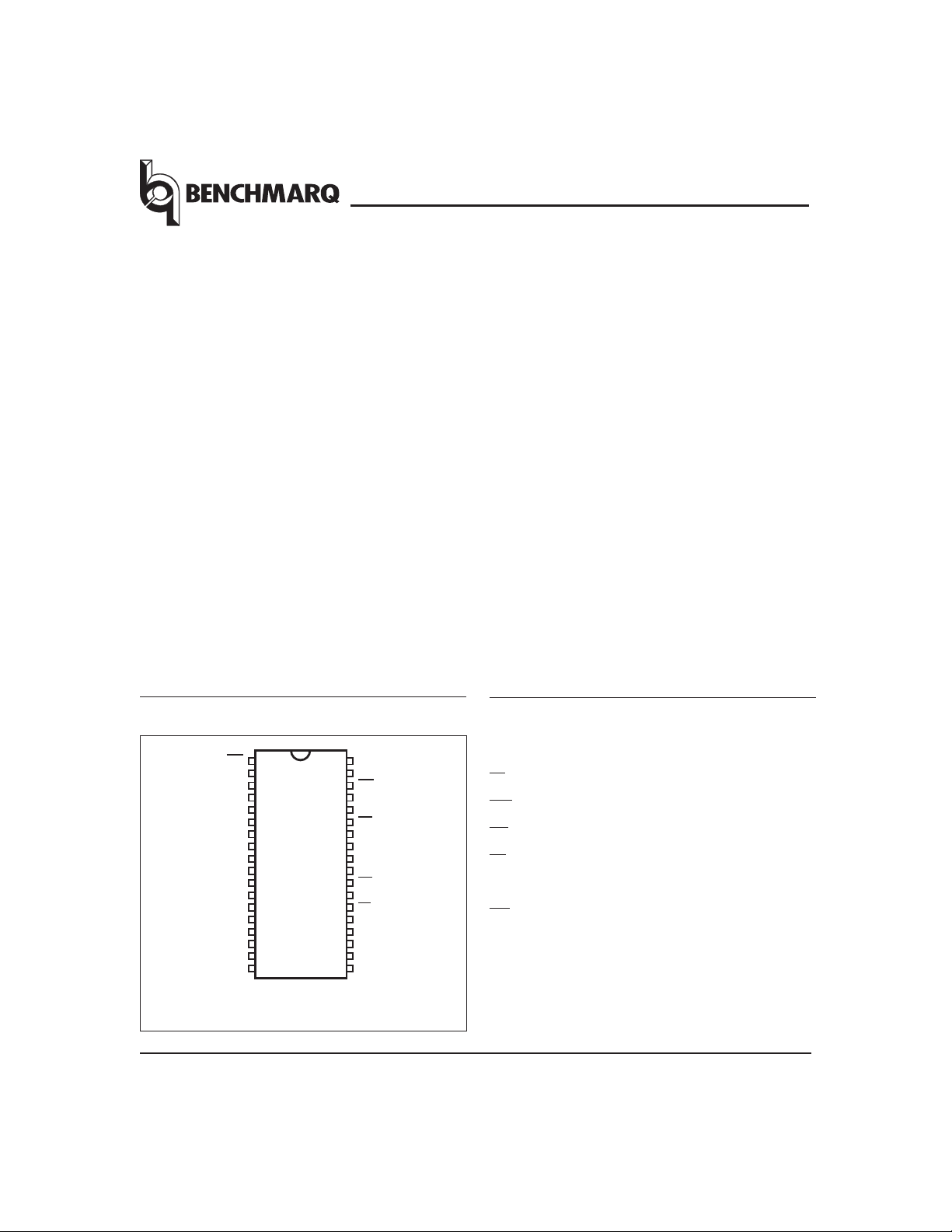
Pin Connections
General Description
The bq4852Y RTC Module is a nonvolatile 4,194,304-bit SRAM organized as 524,288 words by 8 bits with
an integral accessible real-time
clock and CPU supervisor. The CPU
supervisor provides a programmable
watchdog timer and a microprocessor reset. Other features include
alarm, power-fail, and periodic interrupts,andabattery-lowwarning.
The device combines an internal lithium battery, quartz crystal, clock and
power-fail chip, and a full CMOS
SRAM in a plastic 36-pin DIP module. The RTC Module directly replaces industry-standard SRAMs and
also fits into many EPROM and EEPROM sockets without any requirement for special write timing or limitations on the number of write cycles.
Pin Names
Registers for the real-time clock,
alarm and other special functions
are located in registers 7FFF0h–
7FFFFh of the memory array.
The clock and alarm registers are
dual-port read/write SRAM locations that are updated once per second by a clock control circuit from
the internal clock counters. The
dual-port registers allow clock updates to occur without interrupting
normal access to the rest of the
SRAM array.
The bq4852Y also contains a powerfail-detect circuit. The circuit deselects the device whenever V
CC
falls
below tolerance, providing a high degree of data security. The battery is
electrically isolated when shipped
from the factory to provide maximum battery capacity. The battery
remains disconnected until the first
application of VCC.
Aug.1996
RST
1
NC
2
A
3
18
A
4
16
A
5
14
A
6
12
A
7
7
A
8
6
9
A
5
A
10
4
11
A
3
A
12
2
A
13
1
A
14
0
DQ
15
0
DQ
16
1
DQ
17
2
V
18
SS
36-Pin DIP Module
36
35
34
33
32
31
30
29
28
27
26
25
24
23
22
21
20
19
PN485201.eps
V
NC
INT
A
A
WE
A
A
A
A
OE
A
CE
DQ
DQ
DQ
DQ
DQ
CC
15
17
13
8
9
11
10
A0–A
18
Address input
CE Chip enable
RST
Microprocessor reset
WE Write enable
OE Output enable
DQ0–DQ7Data in/data out
7
6
5
4
3
INT Programmable interrupt
V
CC
V
SS
+5 volts
Ground
1
bq4852Y
Functional Description
Figure 1 is a block diagram of the bq4852Y. The following sections describe the bq4852Y functional operation,
including memory and clock interface, data-retention
CE
OE
DQ -DQ
0
AD -AD
0
WE
V
CC
Internal
Battery
Internal
Quartz
Crystal
7
18
P
Bus
I/F
Power-
Fail
Control
Write-
Protect
Time-
Base
Oscillator
4
3
Control/Status
Registers
Clock/Calendar,
Alarm,
and Control Bytes
User Buffer
(16 Bytes)
Storage
Registers
(524,288 Bytes)
modes, power-on reset timing, watchdog timer activation,andinterruptgeneration.
.
.
-
.
.
-
16 1 MUX
:
Reset and
Interrupt
Generator
Clock/Calendar
Update
.
.
-
64648
RST
INT
BD-962
Truth Table
V
CC
(max.) V
<V
CC
(min.) V
>V
CC
(min.) > V
<V
PFD
≤ V
SO
Figure 1. Block Diagram
CE OE WE Mode DQ Power
X X Deselect High Z Standby
XVILWrite D
V
IL
V
IH
V
IH
V
IH
Read D
Read High Z Active
IN
OUT
SO
IH
V
IL
IL
V
IL
X X X Deselect High Z CMOS standby
X X X Deselect High Z Battery-backup mode
2
Active
Active
Aug.1996

bq4852Y
Address Map
The bq4852Y provides 16 bytes of clock and control status
registers and 524,272 bytes of storage RAM.
Figure 2 illustrates the address map for the bq4852Y. Table
1 is a map of the bq4852Y registers, and T able 2 describes
the register bits.
Memory Interface
Read Mode
The bq4852Y is in read mode whenever OE (output enable)
is low and CE (chip enable) is low. The device architecture
allows ripple-through access of data from eight of 4,194,304
locations in the static storage array. Thus, the unique address specified by the 19 address inputs defines which one
of the 524,288 bytes of data is to be accessed. Valid data is
available at the data I/O pins within tAA(address access
time) after the last address input signal is stable, providing
that the CE and OE (output enable) access times are also
satisfied. If the CE and OE access times are not met, valid
data is available after the latter of chip enable access time
(t
) or output enable access time (tOE).
ACE
and OE control the state of the eight three-state data
CE
I/O signals. If the outputs are activated before tAA, the data
lines are driven to an indeterminate state until tAA. If the
address inputs are changed while CE and OE remain low,
16 Bytes
524,272
Bytes
Clock and
Control Status
Registers
Storage
RAM
7FFFF
7FFF0
7FFEF
0000
output data remains valid for t
(output data hold time),
OH
but goes indeterminate until the next address access.
Write Mode
The bq4852Y is in write mode whenever WE and CE are
active. The start of a write is referenced from the latteroccurring falling edge of WE or CE. A write is terminated
by the earlier rising edge of WE or CE. The addresses
must be held valid throughout the cycle. CE or WE must
return high for a minimum of t
from CE or t
WR2
WR1
from
WE prior to the initiation of another read or write cycle.
Data-in must be valid t
main valid for t
DH1
prior to the end of write and re-
DW
or t
afterward. OE should be kept
DH2
high during write cycles to avoid bus contention; although,
if the output bus has been activated by a low on CE and
OE,alowonWEdisablestheoutputstWZafter WE falls.
Data-Retention Mode
With valid VCC applied, the bq4852Y operates as a
conventional static RAM. Should the supply voltage
decay, the RAM automatically power-fail deselects,
write-protecting itself t
All outputs become high impedance, and all inputs are
treated as “don’t care.”
If power-fail detection occurs during a valid access, the
memory cycle continues to completion. If the memory cycle
fails to terminate within time t
0
1
Month
2
3
4
Hours
5
Minutes
6
Seconds
7
Control
8
Watchdog
9
Interrupts
10
Alarm Date
11
Alarm Hours
12
Alarm Minutes
Alarm Seconds
13
Tenths/
14
Hundredths
15
after VCCfalls below V
WPT
, write-protection takes
WPT
Year
Date
Days
Flags
7FFFF
7FFFE
7FFFD
7FFFC
7FFFB
7FFFA
7FFF9
7FFF8
7FFF7
7FFF6
7FFF5
7FFF4
7FFF3
7FFF2
7FFF1
7FFF0
FG4852Y1
PFD
.
Aug.1996
Figure 2. Address Map
3

bq4852Y
place. When VCCdrops below VSO, the control circuit
switches power to the internal energy source, which preserves data.
The internal coin cell maintains data in the bq4852Y after the initial application of V
of at least 10 years when VCCis less than VSO. As system
power returns and VCCrises above V
nected, and the power supply is switched to external VCC.
Write-protection continues for t
allow for processor stabilization. After t
eration can resume.
for an accumulated period
CC
the battery is discon-
SO,
after VCCreaches V
CER
, normal RAM op-
CER
PFD
are inhibited. Once the frozen clock information is retrieved by reading the appropriate clock memory locations, the read bit should be reset to 0 in order to allow
updates to occur from the internal counters. Because
the internal counters are not halted by setting the read
bit, reading the clock locations has no effect on clock accuracy. Once the read bit is reset to 0, within one second
the internal registers update the user-accessible registers with the correct time. A halt command issued dur-
to
ing a clock update allows the update to occur before
freezing the data.
Setting the Clock
Clock Interface
Reading the Clock
The interface to the clock and control registers of the
bq4852Y is the same as that for the general-purpose
storage memory. Once every second, the user-accessible
clock/calendar locations are updated simultaneously
from the internal real time counters. To prevent reading
data in transition, updates to the bq4852Y clock registers should be halted. Updating is halted by setting the
read bit D6 of the control register to 1. As long as the
read bit is 1, updates to user-accessible clock locations
Bit D7 of the control register is the write bit. Like the
read bit, the write bit when set to a 1 halts updates to
the clock/calendar memory locations. Once frozen, the
locations can be written with the desired information in
24-hour BCD format. Resetting the write bit to 0 causes
the written values to be transferred to the internal clock
counters and allows updates to the user-accessible registers to resume within one second. Use the write bit, D7,
only when updating the time registers (7FFFF–7FFF9).
Table 1. bq4842 Clock and Control Register Map
Address D7 D6 D5 D4 D3 D2 D1 D0 Range (h) Register
7FFFF 10 Years Year 00–99 Year
7FFFF X X X 10 Month Month 01–12 Month
7FFFD X X 10 Date Date 01–31 Date
7FFFC X FTE X X X Day 01–07 Days
7FFFB X X 10 Hours Hours 00–23 Hours
7FFFA X 10 Minutes Minutes 00–59 Minutes
7FFF9 OSC 10 Seconds Seconds 00–59 Seconds
7FFF8 W R S Calibration 00–31 Control
7FFF7 WDS BM4 BM3 BM2 BM1 BM0 WD1 WD0 Watchdog
7FFF6 AIE PWRIE ABE PIE RS3 RS2 RS1 RS0 Interrupts
7FFF5 ALM3 X 10-date alarm Alarm date 01–31 Alarm date
7FFF4 ALM2 X 10-hour alarm Alarm hours 00–23 Alarm hours
7FFF3 ALM1 Alarm 10 minutes Alarm minutes 00–59 Alarm minutes
7FFF2 ALM0 Alarm 10 seconds Alarm seconds 00–59 Alarm seconds
7FFF1 0.1 seconds 0.01 seconds 00–99 0.1/0.01 seconds
7FFF0 WDF AF PWRF BLF PF X X X Flags
Notes: X = Unused bits; can be written and read.
Clock/Calendar data in 24-hour BCD format.
BLF = 1 for low battery.
OSC = 1 stops the clock oscillator.
Interrupt enables are cleared on power-up.
Aug.1996
4

Table 2. Clock and Control Register Bits
Bits Description
ABE
AF Alarm interrupt flag
AIE Alarm interrupt enable
ALM0–ALM3 Alarm repeat rate
BLF Battery-low flag
BM0–BM4 Watchdog multiplier
FTE Frequency test mode enable
OSC Oscillatorstop
PF Periodic interrupt flag
PIE Periodic interrupt enable
PWRF Power-fail interrupt flag
PWRIE Power-fail interrupt enable
R Read clock enable
RS0–RS3 Periodic interrupt rate
S Calibration sign
W Write clock enable
WD0–WD1 Watchdog resolution
WDF Watchdog flag
WDS Watchdogsteering
Alarm interrupt enable in
battery-backup mode
Stopping and Starting the Clock Oscillator
The OSC bit in the seconds register turns the clock on or
off. If the bq4852Y is to spend a significant period of
time in storage, the clock oscillator can be turned off to
preserve battery capacity. OSC set to 1 stops the clock
oscillator. When OSC is reset to 0, the clock oscillator is
turned on and clock updates to user-accessible memory
locations occur within one second.
The OSC bit is set to 1 when shipped from the Benchmarq factory.
bq4852Y
adjust the calibration based on the typical operating
temperature of individual applications.
The software calibration bits are located in the control
register. Bits D0–D4 control the magnitude of correction, and bit D5 the direction (positive or negative) of
correction. Assuming that the oscillator is running at
exactly 32,786 Hz, each calibration step of D0–D4 adjusts the clock rate by +4.068 ppm (+10.7 seconds per
month) or -2.034 ppm (-5.35 seconds per month) depending on the value of the sign bit D5. When the sign bit is
1, positive adjustment occurs; a 0 activates negative adjustment. The total range of clock calibration is +5.5 or
-2.75 minutes per month.
Two methods can be used to ascertain how much cali-
bration a given bq4852Y may require in a system. The
first involves simply setting the clock, letting it run for a
month, and then comparing the time to an accurate
known reference like WWV radio broadcasts. Based on
the variation to the standard, the end user can adjust
the clock to match the system’s environment even after
the product is packaged in a non-serviceable enclosure.
The only requirement is a utility that allows the end
user to access the calibration bits in the control register.
The second approach uses a bq4852Y test mode. When
the frequency test mode enable bit FTE in the days register is set to a 1, and the oscillator is running at exactly
32,768 Hz, the LSB of the seconds register toggles at
512 Hz. Any deviation from 512 Hz indicates the degree
and direction of oscillator frequency shift at the test
temperature. For example, a reading of 512.01024 Hz
indicates a (1E6*0.01024)/512 or +20 ppm oscillator frequency error, requiring ten steps of negative calibration
(10*-2.034 or -20.34) or 001010 to be loaded into the calibra-
Calibrating the Clock
The bq4852Y real-time clock is driven by a quartz controlled oscillator with a nominal frequency of 32,768 Hz.
The quartz crystal is contained within the bq4852Y
package along with the battery. The clock accuracy of
the bq4852Y module is tested to be within 20ppm or
about 1 minute per month at 25°C. The oscillation rates
of crystals change with temperature as Figure 3 shows.
To compensate for the frequency shift, the bq4852Y offers onboard software clock calibration. The user can
Aug.1996
Figure 3. Frequency Error
5
 Loading...