

Page 1
User's Guide
SLUUBT8A–June 2018–Revised July 2018
BQ2571x Evaluation Module
The BQ25710EVM-017 and BQ25713EVM-017 evaluation modules (EVM) are SMBus or I2C-controlled
NVDC-1 buck boost charger. The input voltage range is between 3.5 V and 24 V, with a programmable
output of 1–4 cells and a charge output current range of 64 mA to 8.128 A. This EVM does not include the
EV2400 interface device; the EV2400 must be ordered separately to evaluate the BQ2571x EVM.
Contents
1 Introduction ................................................................................................................... 2
1.1 EVM Features....................................................................................................... 2
1.2 General Description ................................................................................................ 2
2 Test Summary................................................................................................................ 5
2.1 Definitions............................................................................................................ 5
2.2 Equipment ........................................................................................................... 5
2.3 Equipment Setup.................................................................................................... 6
2.4 Procedure............................................................................................................ 9
3 Bill of Materials, Board Layout, and Schematics....................................................................... 10
3.1 Bill of Materials .................................................................................................... 10
3.2 Board Assembly Layout .......................................................................................... 13
3.3 Schematic .......................................................................................................... 15
1 EV2400 Connections........................................................................................................ 6
2 Original Test Setup for BMS017 (BQ2571x EVM) ...................................................................... 7
3 Main Window of the BQ2571x Evaluation Software .................................................................... 8
4 EN_OTG ...................................................................................................................... 9
5 Top Assembly............................................................................................................... 13
6 Bottom Assembly........................................................................................................... 14
7 BQ2571x EVM Schematic ................................................................................................ 15
1 I/O Description ............................................................................................................... 3
2 Controls and Key Parameters Setting .................................................................................... 3
3 Recommended Operating Conditions..................................................................................... 4
4 BQ2571x EVM Bill of Materials........................................................................................... 10
Trademarks
USB Type-C is a trademark of USB Implementer's Forum, Inc..
All other trademarks are the property of their respective owners.
List of Figures
List of Tables
SLUUBT8A–June 2018–Revised July 2018
Submit Documentation Feedback
Copyright © 2018, Texas Instruments Incorporated
BQ2571x Evaluation Module
1
Page 2

Introduction
1 Introduction
1.1 EVM Features
This EVM supports the following features:
• Evaluation module for the BQ2571x devices
• Supports 3.5- to 24-V input source
– 3.5- to 24-V, 0- to 6-A input operating range and 1–4 cell battery configuration
– Supports USB2.0, USB 3.0, USB 3.1 (USB Type-C™) and USB_PD
– Supports USB OTG with 3- to 20.8-V adjustable output
– Maximum Power Tracking by Input Voltage and Current Regulation
• Narrow VDC (NVDC) power path management
– Instant-on works with no battery or deeply discharged battery (PG1.0 needs charge-enable
command)
– Battery supplements system when adapter is fully-loaded
• 800-kHz or 1.2-MHz switching frequency for low profile inductor
• SMBus (BQ25710) or I2C (BQ25713) port for optimal system performance and status reporting
• Power and Current Monitor for CPU Throttling
• Safety
– Thermal shutdown
– Input and system overvoltage protection
– MOSFET overcurrent protection
• Accelerate charge time by battery path impedance compensation
• Charge status outputs for LED or host processor
• Maximum power tracking capability by input voltage regulation
• Test points for key signals available for testing purposes. Easy probe hook-up.
• Jumpers available. Easy-to-change connections.
www.ti.com
1.2 General Description
The BQ2571x evaluation modules are complete charger modules for evaluating an SMBUS or I2Ccontrolled buck boost charge using the BQ2571x devices.
The BQ2571x EVM does not include the EV2400 interface board. To evaluate the BQ2571x EVM, order
an EV2400 interface board separately.
The BQ2571x is a synchronous NVDC-1 battery buck boost charge controller, offering a low component
count, high efficiency solution for space-constrained, multi-chemistry battery charging applications.
The NVDC-1 configuration allows the system to be regulated at the battery voltage, but not drop below the
system minimum voltage. The system keeps operating even when the battery is completely discharged or
removed. When load power exceeds the input source rating, the battery supplement mode prevents the
input source from being overloaded.
The BQ2571x charges the battery from a wide range of input sources including a 5-V USB adapter to a
high-voltage USB PD source and traditional adapters.
During power up, the charger sets the converter to buck, boost, or buck-boost configuration based on the
input source and battery conditions. During the charging cycle, the charger automatically transits among
buck, boost, and buck-boost configuration without host control.
The BQ2571x monitors adapter current, battery current, and system power. The flexibly programmed
PROCHOT output goes directly to the CPU for throttle back, when needed.
For more details on register functions, see the data sheets – BQ25710 (SLUSD20) and BQ25713
(SLUSD83).
2
BQ2571x Evaluation Module
Copyright © 2018, Texas Instruments Incorporated
SLUUBT8A–June 2018–Revised July 2018
Submit Documentation Feedback
Page 3
www.ti.com
Table 1 lists the I/O descriptions.
Introduction
Table 1. I/O Description
Jack Description
J1–VIN Input: positive terminal
J1–GND Input: negative terminal (ground terminal)
J2-ILIM_control External converter disable; logic high to pull the ILIM pin down
J2-CHRG_OK CHRG_OK output
J2-ENZ_OTG External OTG disable pin
J2-CELL_control External battery removal control; logic high to pull the CELL pin down
J3–3V3 Onboard 3.3-V output
J3–SDA SMBUS or I2C SDA
J3-SCL SMBUS or I2C SCL
J3-GND Ground
J4-CMPOUT CMPOUT pin output
J4-GND Ground
J4-CMPIN External CMPIN pin input
J5-BAT Connected to battery pack output
J5-GND Ground
J6-SYS Connected to system output
J6-GND Ground
Table 2 displays the controls and key parameters settings.
Table 2. Controls and Key Parameters Setting
Jack Description Factory Setting
JP1
JP7
JP2
JP3
JP4
JP5 Jumper on: Pre-bias ILIM_HIZ
JP6 For input current setting:
JP8 Jumper on: On-board LDO to drive the EVM 3V3
Inrush control setting:
spa1. Bypass inrush control circuit
spa1. JP1 on: bypasses input FETs Q9 and Q10 external selector spa1.
spa1. JP7 top two connection (pin 2 is connected to pin 3): VBUS pin on ACP
spa2. Enable inrush control circuit
spa2. JP1 off: CHRG_OK controls Q9 and Q10 external selector
spa2. JP7 bottom two connection: VBUS pin on V
CELL setting:
spa1S: JP2, JP3, JP4 all open, measure CELL pin voltage 1.2 V
spa2S: JP2 closed, JP3 and JP4 open, measure CELL pin voltage 2.7 V
spa3S: JP3 closed, JP2 and JP4 open, measure CELL pin voltage 3.5 V
spa4S: JP2, JP3 closed, JP4 open, measure CELL pin voltage 4.2 V Bat
sparemoval, short JP4
Jumper off: Ground ILIM_HIZ
spa Jumper on: ILIM_HIZ LOW.
spa Jumper off: Allow pre-bias ILIM_HIZ
Jumper off: disconnect on-board LDO to drive the EVM 3V3
IN
Bypass inrush control circuit:
spaJP1 installed
spaJP7 top two position installed
spa(pin2 is connected pin3)
2S setting: JP2 installed JP3, JP4 all
open
Installed
Not installed
Installed
SLUUBT8A–June 2018–Revised July 2018
Submit Documentation Feedback
Copyright © 2018, Texas Instruments Incorporated
BQ2571x Evaluation Module
3
Page 4
Introduction
Table 3 lists the recommended operating conditions.
Symbol Description MIN TYP MAX Unit
Supply voltage, V
Battery voltage, V
Supply current, I
Output current, I
Operating junction temperature
range, T
www.ti.com
Table 3. Recommended Operating Conditions
IN
BAT
AC
out
J
Input voltage from ac adapter input 3.5 5/12/19 24 V
Voltage applied at VBAT terminal 0 19.2 V
Maximum input current from ac adapter
0 3 A
input
Output current 0 8 A
0 125 °C
4
BQ2571x Evaluation Module
Copyright © 2018, Texas Instruments Incorporated
SLUUBT8A–June 2018–Revised July 2018
Submit Documentation Feedback
Page 5

www.ti.com
2 Test Summary
2.1 Definitions
This procedure details how to configure the BMS017 evaluation board. For the test procedure, the
following naming conventions are followed. Refer to the PWR732 schematic for details.
VXXX: External voltage supply name (VADP, VBT, VSBT)
LOADW: External load name (LOADR, LOADI)
V(TPyyy): Voltage at internal test point TPyyy. For example, V(TP12) means the
V(Jxx): Voltage at jack terminal Jxx.
V(TP(XXX)): Voltage at test point “XXX”. For example, V(ACDET) means the voltage at
V(XXX, YYY): Voltage across point XXX and YYY.
I(JXX(YYY)): Current going out from the YYY terminal of jack XX.
Jxx(BBB): Terminal or pin BBB of jack xx
Jxx ON : Internal jumper Jxx terminals are shorted
Jxx OFF: Internal jumper Jxx terminals are open
Jxx (-YY-) ON: Internal jumper Jxx adjacent terminals marked as “YY” are shorted
Measure: → A,B Check specified parameters A, B. If measured values are not within
Observe → A,B Observe if A, B occurs. If they do not occur, the unit under test has failed.
Test Summary
voltage at TP12.
the test point which is marked as “ACDET”.
specified limits, the unit under test has failed.
Assembly drawings have locations for jumpers, test points, and individual components.
2.2 Equipment
The following list of equipment is required for fully testing the EVM:
1. Power Supplies
A power supply capable of supplying 24 V at 6 A is required. While this part can handle larger voltage
and current, it is not necessary for this procedure.
2. Load #1
A 0- to 20-V/0- to 6-A, system DC electronic load and setting as constant voltage load mode.
3. Load #2
A Kepco load: BOP36-6M, DC 0 to ±36 V, 0 to ±6 A (or higher), or equivalent.
4. Meters
Six Fluke 75 multimeters, (equivalent or better) or: Four equivalent voltage meters and two equivalent
current meters.
5. Computer
A computer with at least one USB port and a USB cable.
6. EV2400 Communication Kit
7. Software
Download and properly install BQstudio (Version: 1.3.85 or newer) from
http://www.ti.com/tool/BQstudio.
SLUUBT8A–June 2018–Revised July 2018
Submit Documentation Feedback
Copyright © 2018, Texas Instruments Incorporated
BQ2571x Evaluation Module
5
Page 6
Test Summary
2.3 Equipment Setup
Use the following guidelines to set up the equipment:
1. Set power supply #1 for 10-V DC, 5-A current limit and then turn off the supply.
2. Connect the output of power supply #1 in series with a current meter to J1 (VIN and GND).
3. Connect a voltage meter across J1 (VIN) and J1 (GND).
4. Connect load #1 in series with a current meter to J6 (VSYS and GND). Connect a voltage meter
across J6 (VSYS and GND). Set 1 A at the constant current mode. Turn off load #1.
5. Connect Load #2 in series with a current meter to J5 (VBAT and GND). Connect a voltage meter
across J5 (VBAT and GND). Set 7 V at KEPCO load output. Turn off Load #2.
NOTE: Add a 47-µF capacitor on the BAT pin when testing without real battery.
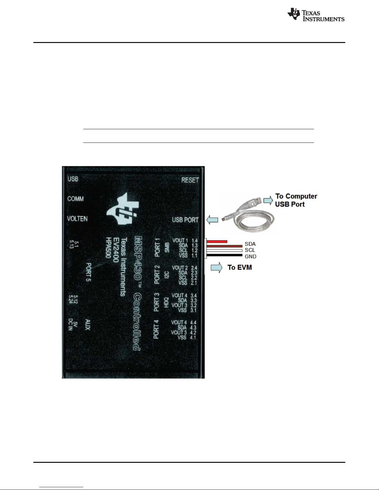
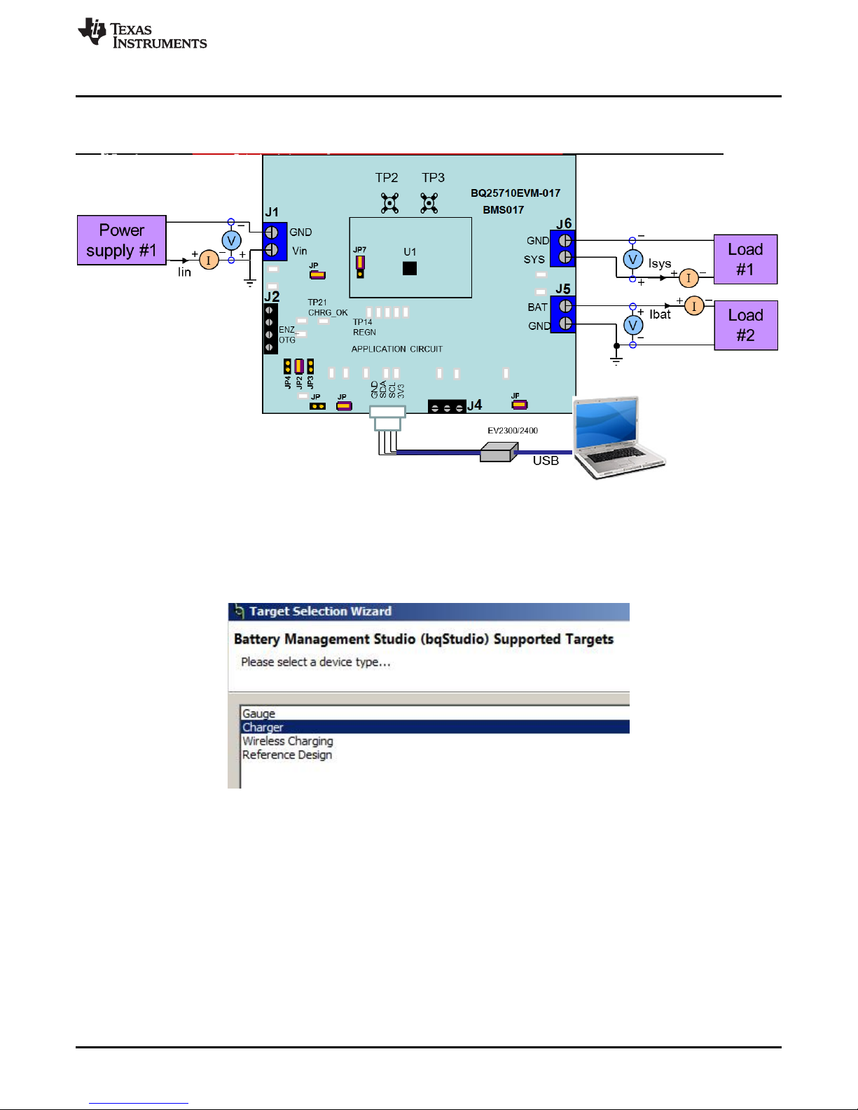
6. Connect J3 to the EV2400. Connect J3 to the SMBus PORT 1 (BQ25710) or I2C PORT 2 (BQ25713)
on the EV2400. The connections are shown in Figure 1.
www.ti.com
The picture shows the SMBus version EVM connection. If using the BQ25713EVM-017, move the connector to the
I2C port.
6
BQ2571x Evaluation Module
Figure 1. EV2400 Connections
Copyright © 2018, Texas Instruments Incorporated
SLUUBT8A–June 2018–Revised July 2018
Submit Documentation Feedback
Page 7
www.ti.com
7. Install jumpers as “JUMPER SET UP”.
Test Summary
After completing these steps , the test setup for BMS017 is as shown in Figure 2.
Figure 2. Original Test Setup for BMS017 (BQ2571x EVM)
8. Turn on the computer and power supply #1. Open the BQstudio software.
a. Select Charger and click the Next button.
b. For SMBus BQ25710, select “Charger_1_00-BQ25710SMB.BQz” on the Select a Target Page. For
I2C BQ25713, select “Charger_1_00-BQ25713I2C.BQz” on the Select a Target Page.
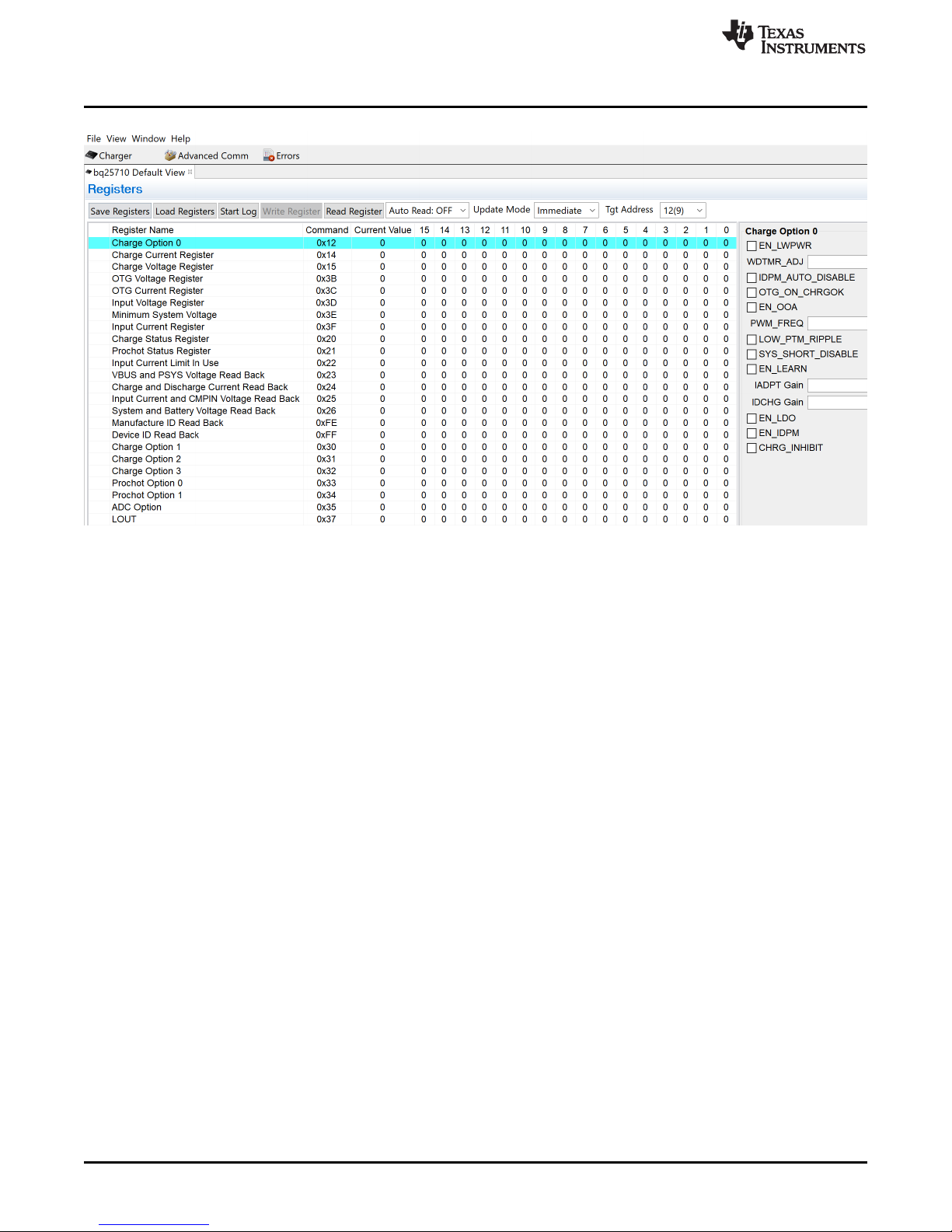
c. After selecting the target device, change “update mode” from “immediate” to “manual”, click “Read
Register” and the following interface is presented.
SLUUBT8A–June 2018–Revised July 2018
Submit Documentation Feedback
Copyright © 2018, Texas Instruments Incorporated
BQ2571x Evaluation Module
7
Page 8
Test Summary
www.ti.com
Figure 3. Main Window of the BQ2571x Evaluation Software
8
BQ2571x Evaluation Module
Copyright © 2018, Texas Instruments Incorporated
SLUUBT8A–June 2018–Revised July 2018
Submit Documentation Feedback
Page 9

www.ti.com
2.4 Procedure
2.4.1 Charge Function
1. Make sure Equipment Setup steps are followed.
2. Set Tgt Address to 12(9) for BQ25710 or D6(6B) for BQ25713
3. Write “020E” to charge option 0 register 0x12H (BQ25710) or 0x00H (BQ25713).
Measure → V(J1(VIN)) = 10 V ±0.5 V
Measure → V(TP28(CHRG_OK)) = 3 V to 4.5 V
Measure → V(TP21(REGN)) = 6 V ±1 V
Measure → V(TP22(ILIM_HIZ)) = 2.2 V
4. Write “0800” to charge current 0x14H (BQ25710) or 0x02H (BQ25713). Turn on load #1.
Measure → V(J6(SYS)) = 8.4 V ±0.5 V
5. Turn on LOAD #2 (VBAT Load).
Measure → V(J5(VBAT)) = 7 V ±0.5 V
Measure → I(J5(VBAT)) = 2 A ±0.5 V
2.4.2 OTG Function
Use the following for OTG function settings:
1. Set EN_OTG high on J2 (EN_OTG) or short TP37 to TP35 (EN_OTG).
2. Connect a 7-V power supply to the VBAT load. Remove the VINpower supply from J1. (Connection
must be physically removed from board).
3. Write the Charge Voltage Register to 0x20D0.
4. Write “0200” to the OTG voltage register. Write “4000” to the OTG current registers.
5. Select EN_OTG in Charge Option 3.
Measure → V(J1(VIN)) = 5 V ±1 V
Test Summary
SLUUBT8A–June 2018–Revised July 2018
Submit Documentation Feedback
Figure 4. EN_OTG
Copyright © 2018, Texas Instruments Incorporated
BQ2571x Evaluation Module
9
Page 10
Bill of Materials, Board Layout, and Schematics
www.ti.com
10
SLUUBT8A–June 2018–Revised July 2018
Submit Documentation Feedback
Copyright © 2018, Texas Instruments Incorporated
BQ2571x Evaluation Module
3 Bill of Materials, Board Layout, and Schematics
This section contains the EVM BOM, board layout images, and schematics.
3.1 Bill of Materials
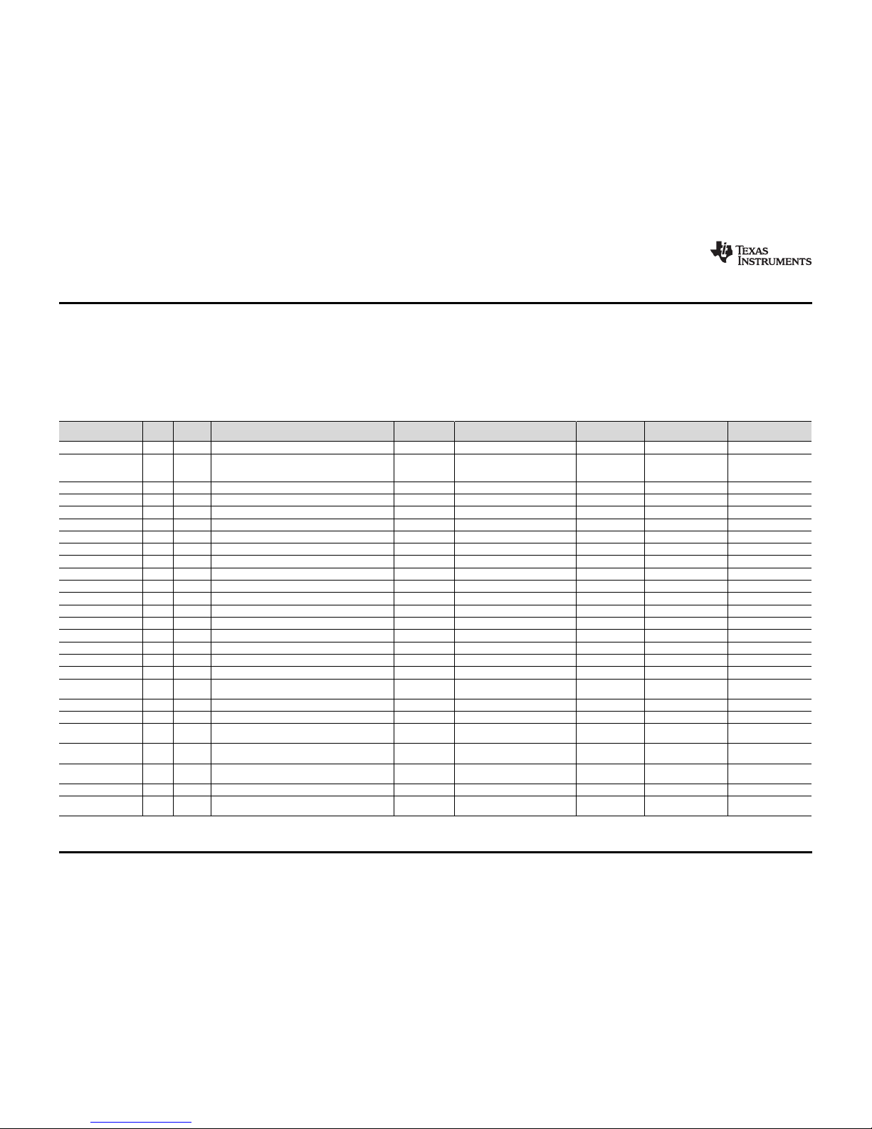
Table 4 lists the BQ2571x EVM bill of materials.
(1)
Unless otherwise noted in the Alternate Part Number or Alternate Manufacturer columns, all parts may be substituted with equivalents.
Table 4. BQ2571x EVM Bill of Materials
(1)
Designator Qty Value Description Package
Reference
Part Number Manufacturer Alternate Part Number Alternate Manufacturer
!PCB1 1 Printed Circuit Board BMS017 Any - C3, C4, C5, C6, C7, C8,
C9, C10, C21, C23, C24,
C44, C45
13 10uF CAP, CERM, 10 µF, 25 V, +/- 10%, X5R, 0805 0805 GRM21BR61E106KA73L Murata
C12,C41 2 0.01uF CAP, CERM, 0.01 µF, 25 V, +/- 10%, X7R, 0603 0603 GRM188R71E103KA01D Murata
C15, C16 2 0.047uF CAP, CERM, 0.047uF, 25V, +/-10%, X7R, 0603 0603 GRM188R71E473KA01D Murata
C17 1 1000pF CAP, CERM, 1000 pF, 25 V, +/- 5%, X7R, 0402 0402 C0402C102J3RACTU Kemet
C18, C29 2 1uF CAP, CERM, 1uF, 25V, +/-10%, X7R, 0603 0603 GRM188R71E105KA12D Murata
C19, C20 2 150pF CAP, CERM, 150 pF, 50 V, +/- 5%, C0G/NP0, 0603 0603 C0603C151J5GACTU Kemet
C22, C27, C38, C39 4 0.1uF CAP, CERM, 0.1uF, 25V, +/-10%, X7R, 0603 0603 GRM188R71E104KA01D Murata
C25 1 0.47uF CAP, CERM, 0.47 µF, 16 V, +/- 10%, X7R, 0805 0805 C0805C474K4RACTU Kemet
C26 1 10uF CAP, CERM, 10 µF, 25 V, +/- 10%, X7R, 1206 1206 GRM31CR71E106KA12L Murata
C28 1 1uF CAP, CERM, 1 µF, 25 V, +/- 10%, X7R, 0603 0603 GRM188R71E105KA12D Murata
C30 1 2.2uF CAP, CERM, 2.2 µF, 35 V, +/- 10%, X5R, 0603 0603 GRM188R6YA225KA12D Murata
C31 1 33pF CAP, CERM, 33 pF, 50 V, +/- 5%, C0G/NP0, 0402 0402 GRM1555C1H330JA01D Murata
C32 1 680pF CAP, CERM, 680 pF, 50 V, +/- 5%, C0G/NP0, 0402 0402 GRM1555C1H681JA01D Murata
C33 1 1800pF CAP, CERM, 1800 pF, 50 V, +/- 10%, X7R, 0402 0402 GRM155R71H182KA01D Murata
C34 1 15pF CAP, CERM, 15 pF, 50 V, +/- 5%, C0G/NP0, 0402 0402 GRM1555C1H150JA01D Murata
C35, C36, C37 3 100pF CAP, CERM, 100pF, 50V, +/-5%, C0G/NP0, 0603 0603 C0603C101J5GAC Kemet
C46, C47 2 0.033uF CAP, CERM, 0.033 µF, 25 V, +/- 10%, X7R, 0603 0603 GRM188R71E333KA01D Murata
C48, C49, C53 3 47uF CAP,Tantalum Polymer, 47 µF, 20 V, +/- 20%, 0.055 ohm,
7343-20 SMD
7343-20 20TQC47MYF Panasonic
D2, D3, D5 3 30V Diode, Schottky, 30V, 0.2A, SOD-323 SOD-323 BAT54HT1G ON Semiconductor
D4 1 Green LED, Green, SMD 1.6x0.8x0.8mm LTST-C190GKT Lite-On
H1, H2, H3, H4 4 Bumpon,Hemisphere, 0.44 X 0.20, Clear Transparent
Bumpon
SJ-5303 (CLEAR) 3M
J1, J5, J6 3 TERMINAL BLOCK 5.08MM VERT 2POS TERM_BLK,
2pos, 5.08mm
ED120/2DS On-Shore
Technology, Inc.
J2 1 Terminal Block, 6A, 3.5mm Pitch, 4-Pos, TH 14x8.2x6.5mm ED555/4DS On-Shore
Technology
J3 1 Header, 100mil, 4x1, R/A, TH 4x1 R/A Header 22-05-3041 Molex
J4 1 Terminal Block, 6A, 3.5mm Pitch, 3-Pos, TH 10.5x8.2x6.5mm ED555/3DS On-Shore
Technology, Inc.
Page 11

www.ti.com
Bill of Materials, Board Layout, and Schematics
11
SLUUBT8A–June 2018–Revised July 2018
Submit Documentation Feedback
Copyright © 2018, Texas Instruments Incorporated
BQ2571x Evaluation Module
Table 4. BQ2571x EVM Bill of Materials
(1)
(continued)
Designator Qty Value Description Package
Reference
Part Number Manufacturer Alternate Part Number Alternate Manufacturer
JP1, JP2, JP3, JP4, JP5,
JP6, JP8
7 Header, 100mil, 2x1, Gold plated, TH Header, 2x1,
100mil
5-146261-1 TE Connectivity
JP7 1 Header, 100mil, 3x1, Tin, TH Header, 3 PIN,
100mil, Tin
PEC03SAAN Sullins Connector
Solutions
L1 1 2.2uH Inductor, Wirewound, Powdered Iron, 2.2 µH, 8.5 A, 0.0203
ohm, SMD
9.2x8.5mm 74437356022 Wurth Elektronik IHLP3232CZER2R2M01 Vishay-Dale
LBL1 1 Thermal Transfer Printable Labels, 0.650" W x 0.200" H -
10,000 per roll
PCB Label
0.650"H x
0.200"W
THT-14-423-10 Brady - -
Q1, Q2, Q3, Q4 4 30V MOSFET, N-CH, 30 V, 12 A, SON 3.3x3.3mm SON 3.3x3.3mm CSD17551Q3A Texas Instruments None
Q5, Q6 2 -30V MOSFET, P-CH, -30 V, -8.5 A, 8-PowerVDFN 8-PowerVDFN DMP3035SFG-7 Diodes Inc. DMG7401SFG-7 Diodes, Inc.
Q7 1 -20V MOSFET,P-CH, -20 V, -15 A, SON 3.3x3.3mm SON 3.3x3.3mm CSD25402Q3A Texas Instruments None
Q9 1 50 V Transistor,NPN/PNP Pair, 50 V, 0.05 A, SC-74R SC-74R DCX124EK-7-F Diodes Inc.
Q10, Q12 2 60V MOSFET, N-CH, 60V, 0.26A, SOT-23 SOT-23 2N7002ET1G ON Semiconductor None
Q11 1 60V MOSFET, N-CH, 60 V, 0.26 A, SOT-23 SOT-23 2N7002ET1G ON Semiconductor None
R2, R8 2 0.01 RES,0.01 ohm, 1%, 1W, 1206 1206 WSLP1206R0100FEA Vishay-Dale
R3, R4 2 3.9 RES, 3.9 ohm, 5%, 0.25W, 1206 1206 CRCW12063R90JNEA Vishay-Dale
R9, R28 2 100k RES, 100 k, 1%, 0.1 W, 0603 0603 RC0603FR-07100KL Yageo America
R10, R38 2 10.0 RES,10.0 ohm, 1%, 0.25W, 1206 1206 ERJ-8ENF10R0V Panasonic
R11, R12 2 4.99 RES,4.99, 1%, 0.1 W, 0603 0603 CRCW06034R99FKEA Vishay-Dale
R13 1 1.0 RES, 1.0, 5%, 0.125 W, 0805 0805 CRCW08051R00JNEA Vishay-Dale
R14 1 20k RES, 20 k, 5%, 0.1 W, 0603 0603 CRCW060320K0JNEA Vishay-Dale
R15, R16 2 10 RES, 10, 5%, 0.1 W, 0603 0603 CRCW060310R0JNEA Vishay-Dale
R17 1 10k RES, 10 k, 5%, 0.1 W, 0603 0603 CRCW060310K0JNEA Vishay-Dale
R18 1 10.0 RES,10.0 ohm, 1%, 0.1W, 0603 0603 CRCW060310R0FKEA Vishay-Dale
R19, R26 2 383k RES, 383 k, 1%, 0.1 W, 0603 0603 CRCW0603383KFKEA Vishay-Dale
R20 1 120k RES, 120 k, 1%, 0.1 W, 0603 0603 RC0603FR-07120KL Yageo America
R21 1 64.9k RES, 64.9 k, 1%, 0.1 W, 0603 0603 RC0603FR-0764K9L Yageo America
R22 1 40.2k RES, 40.2 k, 1%, 0.063 W, 0402 0402 CRCW040240K2FKED Vishay-Dale
R23 1 10.0k RES, 10.0 k, 1%, 0.063 W, 0402 0402 CRCW040210K0FKED Vishay-Dale
R24 1 280k RES, 280 k, 1%, 0.1 W, 0603 0603 CRCW0603280KFKEA Vishay-Dale
R25 1 10.0k RES, 10.0 k, 1%, 0.1 W, 0603 0603 CRCW060310K0FKEA Vishay-Dale
R27 1 220k RES, 220 k, 1%, 0.1 W, 0603 0603 RC0603FR-07220KL Yageo America
R29 1 300k RES, 300 k, 1%, 0.1 W, 0603 0603 CRCW0603300KFKEA Vishay-Dale
R30 1 137k RES, 137 k, 1%, 0.1 W, 0603 0603 RC0603FR-07137KL Yageo America
R31 1 100 RES, 100, 1%, 0.1 W, 0603 0603 CRCW0603100RFKEA Vishay-Dale
R32, R33, R35, R39 4 10.0k RES, 10.0k ohm, 1%, 0.1W, 0603 0603 CRCW060310K0FKEA Vishay-Dale
R34 1 30.1k RES, 30.1k ohm, 1%, 0.1W, 0603 0603 CRCW060330K1FKEA Vishay-Dale
R36 1 2.00k RES, 2.00k ohm, 1%, 0.1W, 0603 0603 CRCW06032K00FKEA Vishay-Dale
R40 1 2.0Meg RES, 2.0 M, 5%, 0.1 W, 0603 0603 CRCW06032M00JNEA Vishay-Dale
Page 12

Bill of Materials, Board Layout, and Schematics
www.ti.com
12
SLUUBT8A–June 2018–Revised July 2018
Submit Documentation Feedback
Copyright © 2018, Texas Instruments Incorporated
BQ2571x Evaluation Module
Table 4. BQ2571x EVM Bill of Materials
(1)
(continued)
Designator Qty Value Description Package
Reference
Part Number Manufacturer Alternate Part Number Alternate Manufacturer
SH-JP1, SH-JP2, SHJP3, SH-JP4, SH-JP5,
SH-JP6, SH-JP7, SH-JP8
8 1x2 Shunt, 100mil, Gold plated, Black Shunt 969102-0000-DA 3M SNT-100-BK-G Samtec
TP1, TP6, TP7, TP10,
TP11, TP13, TP14
7 White Test Point, Miniature, White, TH White Miniature
Testpoint
5002 Keystone
TP2, TP3, TP4, TP5,
TP9, TP12, TP15, TP16,
TP17, TP18, TP19, TP20,
TP21, TP22, TP23, TP24,
TP25, TP26, TP27, TP28,
TP29, TP30, TP31, TP32,
TP33, TP34, TP35, TP36,
TP37, TP38, TP39, TP40
32 SMT Test Point, Miniature, SMT Testpoint_Keysto
ne_Miniature
5015 Keystone
U1 1 SMBus/I2C Multi-Chemistry Battery Buck-Boost Charge
Controller With System Power Monitor and Processor Hot
Monitor, RSN0032B (WQFN-32)
RSN0032B BQ25710RSNR for BQ25710EVM-017
or
BQ25713RSNR for BQ25713EVM-017
Texas Instruments BQ25710RSNT TexasInstruments
U2 1 100 mA, Quasi Low-Dropout Linear Voltage Regulator, 3-
pin SOT-23, Pb-Free
MF03A LM3480IM3-3.3/NOPB Texas Instruments
Z1 1 26V Diode, TVS, Bi, 26 V, 400 W, SMA SMA SMAJ26CA Littelfuse
C1 0 15pF CAP, CERM, 15 pF, 50 V, +/- 5%, C0G/NP0, 0603 0603 C0603C150J5GACTU Kemet
C2 0 47uF CAP, Aluminum Polymer, 47 µF, 25 V, +/- 20%, 0.03 ohm,
F61 SMD
F61 25SVPF47M Panasonic
C11 0 0.01uF CAP, CERM, 0.01 µF, 25 V, +/- 10%, X7R, 0603 0603 GRM188R71E103KA01D Murata
C13, C14 0 330pF CAP, CERM, 330 pF, 50 V, +/- 10%, X7R, 0603 0603 GRM188R71H331KA01D Murata
C21, C40, C42, C43 0 10uF CAP, CERM, 10 µF, 25 V, +/- 10%, X5R, 0805 0805 GRM21BR61E106KA73L Murata
C41 0 0.01uF CAP, CERM, 0.01uF, 25V, +/-10%, X7R, 0603 0603 GRM188R71E103KA01D Murata
D1 0 20V Diode, Schottky, 20 V, 2 A, SMA SMA B220A-13-F Diodes Inc.
FID1, FID2, FID3, FID4,
FID5, FID6
0 Fiducial mark. There is nothing to buy or mount. Fiducial N/A N/A
R1 0 0 RES, 0 ohm, 5%, 0.1W, 0603 0603 CRCW06030000Z0EA Vishay-Dale
R5, R6 0 56 RES, 56, 5%, 0.1 W, 0603 0603 CRCW060356R0JNEA Vishay-Dale
R37 0 10.0k RES, 10.0k ohm, 1%, 0.1W, 0603 0603 CRCW060310K0FKEA Vishay-Dale
Notes: Unless otherwise noted in the Alternate Part Number and/or Alternate Manufacturer columns, all parts may be substituted with equivalents.
Page 13

www.ti.com
3.2 Board Assembly Layout
Figure 5 and Figure 6 illustrate the board assembly layout images.
Bill of Materials, Board Layout, and Schematics
SLUUBT8A–June 2018–Revised July 2018
Submit Documentation Feedback
Figure 5. Top Assembly
Copyright © 2018, Texas Instruments Incorporated
BQ2571x Evaluation Module
13
Page 14

Bill of Materials, Board Layout, and Schematics
www.ti.com
14
BQ2571x Evaluation Module
Figure 6. Bottom Assembly
Copyright © 2018, Texas Instruments Incorporated
SLUUBT8A–June 2018–Revised July 2018
Submit Documentation Feedback
Page 15

www.ti.com
Bill of Materials, Board Layout, and Schematics
15
SLUUBT8A–June 2018–Revised July 2018
Submit Documentation Feedback
Copyright © 2018, Texas Instruments Incorporated
BQ2571x Evaluation Module
3.3 Schematic
Figure 7 shows the EVM schematic.
Figure 7. BQ2571x EVM Schematic
Page 16

Revision History
www.ti.com
Revision History
NOTE: Page numbers for previous revisions may differ from page numbers in the current version.
Changes from Original (June 2018) to A Revision ......................................................................................................... Page
• Deleted Advance Information............................................................................................................ 1
16
Revision History
Copyright © 2018, Texas Instruments Incorporated
SLUUBT8A–June 2018–Revised July 2018
Submit Documentation Feedback
Page 17

STANDARD TERMS FOR EVALUATION MODULES
1. Delivery: TI delivers TI evaluation boards, kits, or modules, including any accompanying demonstration software, components, and/or
documentation which may be provided together or separately (collectively, an “EVM” or “EVMs”) to the User (“User”) in accordance
with the terms set forth herein. User's acceptance of the EVM is expressly subject to the following terms.
1.1 EVMs are intended solely for product or software developers for use in a research and development setting to facilitate feasibility
evaluation, experimentation, or scientific analysis of TI semiconductors products. EVMs have no direct function and are not
finished products. EVMs shall not be directly or indirectly assembled as a part or subassembly in any finished product. For
clarification, any software or software tools provided with the EVM (“Software”) shall not be subject to the terms and conditions
set forth herein but rather shall be subject to the applicable terms that accompany such Software
1.2 EVMs are not intended for consumer or household use. EVMs may not be sold, sublicensed, leased, rented, loaned, assigned,
or otherwise distributed for commercial purposes by Users, in whole or in part, or used in any finished product or production
system.
2 Limited Warranty and Related Remedies/Disclaimers:
2.1 These terms do not apply to Software. The warranty, if any, for Software is covered in the applicable Software License
Agreement.
2.2 TI warrants that the TI EVM will conform to TI's published specifications for ninety (90) days after the date TI delivers such EVM
to User. Notwithstanding the foregoing, TI shall not be liable for a nonconforming EVM if (a) the nonconformity was caused by
neglect, misuse or mistreatment by an entity other than TI, including improper installation or testing, or for any EVMs that have
been altered or modified in any way by an entity other than TI, (b) the nonconformity resulted from User's design, specifications
or instructions for such EVMs or improper system design, or (c) User has not paid on time. Testing and other quality control
techniques are used to the extent TI deems necessary. TI does not test all parameters of each EVM.
User's claims against TI under this Section 2 are void if User fails to notify TI of any apparent defects in the EVMs within ten (10)
business days after delivery, or of any hidden defects with ten (10) business days after the defect has been detected.
2.3 TI's sole liability shall be at its option to repair or replace EVMs that fail to conform to the warranty set forth above, or credit
User's account for such EVM. TI's liability under this warranty shall be limited to EVMs that are returned during the warranty
period to the address designated by TI and that are determined by TI not to conform to such warranty. If TI elects to repair or
replace such EVM, TI shall have a reasonable time to repair such EVM or provide replacements. Repaired EVMs shall be
warranted for the remainder of the original warranty period. Replaced EVMs shall be warranted for a new full ninety (90) day
warranty period.
3 Regulatory Notices:
3.1 United States
3.1.1 Notice applicable to EVMs not FCC-Approved:
FCC NOTICE: This kit is designed to allow product developers to evaluate electronic components, circuitry, or software
associated with the kit to determine whether to incorporate such items in a finished product and software developers to write
software applications for use with the end product. This kit is not a finished product and when assembled may not be resold or
otherwise marketed unless all required FCC equipment authorizations are first obtained. Operation is subject to the condition
that this product not cause harmful interference to licensed radio stations and that this product accept harmful interference.
Unless the assembled kit is designed to operate under part 15, part 18 or part 95 of this chapter, the operator of the kit must
operate under the authority of an FCC license holder or must secure an experimental authorization under part 5 of this chapter.
3.1.2 For EVMs annotated as FCC – FEDERAL COMMUNICATIONS COMMISSION Part 15 Compliant:
CAUTION
This device complies with part 15 of the FCC Rules. Operation is subject to the following two conditions: (1) This device may not
cause harmful interference, and (2) this device must accept any interference received, including interference that may cause
undesired operation.
Changes or modifications not expressly approved by the party responsible for compliance could void the user's authority to
operate the equipment.
FCC Interference Statement for Class A EVM devices
NOTE: This equipment has been tested and found to comply with the limits for a Class A digital device, pursuant to part 15 of
the FCC Rules. These limits are designed to provide reasonable protection against harmful interference when the equipment is
operated in a commercial environment. This equipment generates, uses, and can radiate radio frequency energy and, if not
installed and used in accordance with the instruction manual, may cause harmful interference to radio communications.
Operation of this equipment in a residential area is likely to cause harmful interference in which case the user will be required to
correct the interference at his own expense.
Page 18

FCC Interference Statement for Class B EVM devices
NOTE: This equipment has been tested and found to comply with the limits for a Class B digital device, pursuant to part 15 of
the FCC Rules. These limits are designed to provide reasonable protection against harmful interference in a residential
installation. This equipment generates, uses and can radiate radio frequency energy and, if not installed and used in accordance
with the instructions, may cause harmful interference to radio communications. However, there is no guarantee that interference
will not occur in a particular installation. If this equipment does cause harmful interference to radio or television reception, which
can be determined by turning the equipment off and on, the user is encouraged to try to correct the interference by one or more
of the following measures:
• Reorient or relocate the receiving antenna.
• Increase the separation between the equipment and receiver.
• Connect the equipment into an outlet on a circuit different from that to which the receiver is connected.
• Consult the dealer or an experienced radio/TV technician for help.
3.2 Canada
3.2.1 For EVMs issued with an Industry Canada Certificate of Conformance to RSS-210 or RSS-247
Concerning EVMs Including Radio Transmitters:
This device complies with Industry Canada license-exempt RSSs. Operation is subject to the following two conditions:
(1) this device may not cause interference, and (2) this device must accept any interference, including interference that may
cause undesired operation of the device.
Concernant les EVMs avec appareils radio:
Le présent appareil est conforme aux CNR d'Industrie Canada applicables aux appareils radio exempts de licence. L'exploitation
est autorisée aux deux conditions suivantes: (1) l'appareil ne doit pas produire de brouillage, et (2) l'utilisateur de l'appareil doit
accepter tout brouillage radioélectrique subi, même si le brouillage est susceptible d'en compromettre le fonctionnement.
Concerning EVMs Including Detachable Antennas:
Under Industry Canada regulations, this radio transmitter may only operate using an antenna of a type and maximum (or lesser)
gain approved for the transmitter by Industry Canada. To reduce potential radio interference to other users, the antenna type
and its gain should be so chosen that the equivalent isotropically radiated power (e.i.r.p.) is not more than that necessary for
successful communication. This radio transmitter has been approved by Industry Canada to operate with the antenna types
listed in the user guide with the maximum permissible gain and required antenna impedance for each antenna type indicated.
Antenna types not included in this list, having a gain greater than the maximum gain indicated for that type, are strictly prohibited
for use with this device.
Concernant les EVMs avec antennes détachables
Conformément à la réglementation d'Industrie Canada, le présent émetteur radio peut fonctionner avec une antenne d'un type et
d'un gain maximal (ou inférieur) approuvé pour l'émetteur par Industrie Canada. Dans le but de réduire les risques de brouillage
radioélectrique à l'intention des autres utilisateurs, il faut choisir le type d'antenne et son gain de sorte que la puissance isotrope
rayonnée équivalente (p.i.r.e.) ne dépasse pas l'intensité nécessaire à l'établissement d'une communication satisfaisante. Le
présent émetteur radio a été approuvé par Industrie Canada pour fonctionner avec les types d'antenne énumérés dans le
manuel d’usage et ayant un gain admissible maximal et l'impédance requise pour chaque type d'antenne. Les types d'antenne
non inclus dans cette liste, ou dont le gain est supérieur au gain maximal indiqué, sont strictement interdits pour l'exploitation de
l'émetteur
3.3 Japan
3.3.1 Notice for EVMs delivered in Japan: Please see http://www.tij.co.jp/lsds/ti_ja/general/eStore/notice_01.page 日本国内に
輸入される評価用キット、ボードについては、次のところをご覧ください。
http://www.tij.co.jp/lsds/ti_ja/general/eStore/notice_01.page
3.3.2 Notice for Users of EVMs Considered “Radio Frequency Products” in Japan: EVMs entering Japan may not be certified
by TI as conforming to Technical Regulations of Radio Law of Japan.
If User uses EVMs in Japan, not certified to Technical Regulations of Radio Law of Japan, User is required to follow the
instructions set forth by Radio Law of Japan, which includes, but is not limited to, the instructions below with respect to EVMs
(which for the avoidance of doubt are stated strictly for convenience and should be verified by User):
1. Use EVMs in a shielded room or any other test facility as defined in the notification #173 issued by Ministry of Internal
Affairs and Communications on March 28, 2006, based on Sub-section 1.1 of Article 6 of the Ministry’s Rule for
Enforcement of Radio Law of Japan,
2. Use EVMs only after User obtains the license of Test Radio Station as provided in Radio Law of Japan with respect to
EVMs, or
3. Use of EVMs only after User obtains the Technical Regulations Conformity Certification as provided in Radio Law of Japan
with respect to EVMs. Also, do not transfer EVMs, unless User gives the same notice above to the transferee. Please note
that if User does not follow the instructions above, User will be subject to penalties of Radio Law of Japan.
Page 19

【無線電波を送信する製品の開発キットをお使いになる際の注意事項】 開発キットの中には技術基準適合証明を受けて
いないものがあります。 技術適合証明を受けていないもののご使用に際しては、電波法遵守のため、以下のいずれかの
措置を取っていただく必要がありますのでご注意ください。
1. 電波法施行規則第6条第1項第1号に基づく平成18年3月28日総務省告示第173号で定められた電波暗室等の試験設備でご使用
いただく。
2. 実験局の免許を取得後ご使用いただく。
3. 技術基準適合証明を取得後ご使用いただく。
なお、本製品は、上記の「ご使用にあたっての注意」を譲渡先、移転先に通知しない限り、譲渡、移転できないものとします。
上記を遵守頂けない場合は、電波法の罰則が適用される可能性があることをご留意ください。 日本テキサス・イ
ンスツルメンツ株式会社
東京都新宿区西新宿6丁目24番1号
西新宿三井ビル
3.3.3 Notice for EVMs for Power Line Communication: Please see http://www.tij.co.jp/lsds/ti_ja/general/eStore/notice_02.page
電力線搬送波通信についての開発キットをお使いになる際の注意事項については、次のところをご覧ください。http:/
/www.tij.co.jp/lsds/ti_ja/general/eStore/notice_02.page
3.4 European Union
3.4.1 For EVMs subject to EU Directive 2014/30/EU (Electromagnetic Compatibility Directive):
This is a class A product intended for use in environments other than domestic environments that are connected to a
low-voltage power-supply network that supplies buildings used for domestic purposes. In a domestic environment this
product may cause radio interference in which case the user may be required to take adequate measures.
4 EVM Use Restrictions and Warnings:
4.1 EVMS ARE NOT FOR USE IN FUNCTIONAL SAFETY AND/OR SAFETY CRITICAL EVALUATIONS, INCLUDING BUT NOT
LIMITED TO EVALUATIONS OF LIFE SUPPORT APPLICATIONS.
4.2 User must read and apply the user guide and other available documentation provided by TI regarding the EVM prior to handling
or using the EVM, including without limitation any warning or restriction notices. The notices contain important safety information
related to, for example, temperatures and voltages.
4.3 Safety-Related Warnings and Restrictions:
4.3.1 User shall operate the EVM within TI’s recommended specifications and environmental considerations stated in the user
guide, other available documentation provided by TI, and any other applicable requirements and employ reasonable and
customary safeguards. Exceeding the specified performance ratings and specifications (including but not limited to input
and output voltage, current, power, and environmental ranges) for the EVM may cause personal injury or death, or
property damage. If there are questions concerning performance ratings and specifications, User should contact a TI
field representative prior to connecting interface electronics including input power and intended loads. Any loads applied
outside of the specified output range may also result in unintended and/or inaccurate operation and/or possible
permanent damage to the EVM and/or interface electronics. Please consult the EVM user guide prior to connecting any
load to the EVM output. If there is uncertainty as to the load specification, please contact a TI field representative.
During normal operation, even with the inputs and outputs kept within the specified allowable ranges, some circuit
components may have elevated case temperatures. These components include but are not limited to linear regulators,
switching transistors, pass transistors, current sense resistors, and heat sinks, which can be identified using the
information in the associated documentation. When working with the EVM, please be aware that the EVM may become
very warm.
4.3.2 EVMs are intended solely for use by technically qualified, professional electronics experts who are familiar with the
dangers and application risks associated with handling electrical mechanical components, systems, and subsystems.
User assumes all responsibility and liability for proper and safe handling and use of the EVM by User or its employees,
affiliates, contractors or designees. User assumes all responsibility and liability to ensure that any interfaces (electronic
and/or mechanical) between the EVM and any human body are designed with suitable isolation and means to safely
limit accessible leakage currents to minimize the risk of electrical shock hazard. User assumes all responsibility and
liability for any improper or unsafe handling or use of the EVM by User or its employees, affiliates, contractors or
designees.
4.4 User assumes all responsibility and liability to determine whether the EVM is subject to any applicable international, federal,
state, or local laws and regulations related to User’s handling and use of the EVM and, if applicable, User assumes all
responsibility and liability for compliance in all respects with such laws and regulations. User assumes all responsibility and
liability for proper disposal and recycling of the EVM consistent with all applicable international, federal, state, and local
requirements.
5. Accuracy of Information: To the extent TI provides information on the availability and function of EVMs, TI attempts to be as accurate
as possible. However, TI does not warrant the accuracy of EVM descriptions, EVM availability or other information on its websites as
accurate, complete, reliable, current, or error-free.
Page 20

6. Disclaimers:
6.1 EXCEPT AS SET FORTH ABOVE, EVMS AND ANY MATERIALS PROVIDED WITH THE EVM (INCLUDING, BUT NOT
LIMITED TO, REFERENCE DESIGNS AND THE DESIGN OF THE EVM ITSELF) ARE PROVIDED "AS IS" AND "WITH ALL
FAULTS." TI DISCLAIMS ALL OTHER WARRANTIES, EXPRESS OR IMPLIED, REGARDING SUCH ITEMS, INCLUDING BUT
NOT LIMITED TO ANY EPIDEMIC FAILURE WARRANTY OR IMPLIED WARRANTIES OF MERCHANTABILITY OR FITNESS
FOR A PARTICULAR PURPOSE OR NON-INFRINGEMENT OF ANY THIRD PARTY PATENTS, COPYRIGHTS, TRADE
SECRETS OR OTHER INTELLECTUAL PROPERTY RIGHTS.
6.2 EXCEPT FOR THE LIMITED RIGHT TO USE THE EVM SET FORTH HEREIN, NOTHING IN THESE TERMS SHALL BE
CONSTRUED AS GRANTING OR CONFERRING ANY RIGHTS BY LICENSE, PATENT, OR ANY OTHER INDUSTRIAL OR
INTELLECTUAL PROPERTY RIGHT OF TI, ITS SUPPLIERS/LICENSORS OR ANY OTHER THIRD PARTY, TO USE THE
EVM IN ANY FINISHED END-USER OR READY-TO-USE FINAL PRODUCT, OR FOR ANY INVENTION, DISCOVERY OR
IMPROVEMENT, REGARDLESS OF WHEN MADE, CONCEIVED OR ACQUIRED.
7. USER'S INDEMNITY OBLIGATIONS AND REPRESENTATIONS. USER WILL DEFEND, INDEMNIFY AND HOLD TI, ITS
LICENSORS AND THEIR REPRESENTATIVES HARMLESS FROM AND AGAINST ANY AND ALL CLAIMS, DAMAGES, LOSSES,
EXPENSES, COSTS AND LIABILITIES (COLLECTIVELY, "CLAIMS") ARISING OUT OF OR IN CONNECTION WITH ANY
HANDLING OR USE OF THE EVM THAT IS NOT IN ACCORDANCE WITH THESE TERMS. THIS OBLIGATION SHALL APPLY
WHETHER CLAIMS ARISE UNDER STATUTE, REGULATION, OR THE LAW OF TORT, CONTRACT OR ANY OTHER LEGAL
THEORY, AND EVEN IF THE EVM FAILS TO PERFORM AS DESCRIBED OR EXPECTED.
8. Limitations on Damages and Liability:
8.1 General Limitations. IN NO EVENT SHALL TI BE LIABLE FOR ANY SPECIAL, COLLATERAL, INDIRECT, PUNITIVE,
INCIDENTAL, CONSEQUENTIAL, OR EXEMPLARY DAMAGES IN CONNECTION WITH OR ARISING OUT OF THESE
TERMS OR THE USE OF THE EVMS , REGARDLESS OF WHETHER TI HAS BEEN ADVISED OF THE POSSIBILITY OF
SUCH DAMAGES. EXCLUDED DAMAGES INCLUDE, BUT ARE NOT LIMITED TO, COST OF REMOVAL OR
REINSTALLATION, ANCILLARY COSTS TO THE PROCUREMENT OF SUBSTITUTE GOODS OR SERVICES, RETESTING,
OUTSIDE COMPUTER TIME, LABOR COSTS, LOSS OF GOODWILL, LOSS OF PROFITS, LOSS OF SAVINGS, LOSS OF
USE, LOSS OF DATA, OR BUSINESS INTERRUPTION. NO CLAIM, SUIT OR ACTION SHALL BE BROUGHT AGAINST TI
MORE THAN TWELVE (12) MONTHS AFTER THE EVENT THAT GAVE RISE TO THE CAUSE OF ACTION HAS
OCCURRED.
8.2 Specific Limitations. IN NO EVENT SHALL TI'S AGGREGATE LIABILITY FROM ANY USE OF AN EVM PROVIDED
HEREUNDER, INCLUDING FROM ANY WARRANTY, INDEMITY OR OTHER OBLIGATION ARISING OUT OF OR IN
CONNECTION WITH THESE TERMS, , EXCEED THE TOTAL AMOUNT PAID TO TI BY USER FOR THE PARTICULAR
EVM(S) AT ISSUE DURING THE PRIOR TWELVE (12) MONTHS WITH RESPECT TO WHICH LOSSES OR DAMAGES ARE
CLAIMED. THE EXISTENCE OF MORE THAN ONE CLAIM SHALL NOT ENLARGE OR EXTEND THIS LIMIT.
9. Return Policy. Except as otherwise provided, TI does not offer any refunds, returns, or exchanges. Furthermore, no return of EVM(s)
will be accepted if the package has been opened and no return of the EVM(s) will be accepted if they are damaged or otherwise not in
a resalable condition. If User feels it has been incorrectly charged for the EVM(s) it ordered or that delivery violates the applicable
order, User should contact TI. All refunds will be made in full within thirty (30) working days from the return of the components(s),
excluding any postage or packaging costs.
10. Governing Law: These terms and conditions shall be governed by and interpreted in accordance with the laws of the State of Texas,
without reference to conflict-of-laws principles. User agrees that non-exclusive jurisdiction for any dispute arising out of or relating to
these terms and conditions lies within courts located in the State of Texas and consents to venue in Dallas County, Texas.
Notwithstanding the foregoing, any judgment may be enforced in any United States or foreign court, and TI may seek injunctive relief
in any United States or foreign court.
Mailing Address: Texas Instruments, Post Office Box 655303, Dallas, Texas 75265
Copyright © 2018, Texas Instruments Incorporated
Page 21

IMPORTANT NOTICE FOR TI DESIGN INFORMATION AND RESOURCES
Texas Instruments Incorporated (‘TI”) technical, application or other design advice, services or information, including, but not limited to,
reference designs and materials relating to evaluation modules, (collectively, “TI Resources”) are intended to assist designers who are
developing applications that incorporate TI products; by downloading, accessing or using any particular TI Resource in any way, you
(individually or, if you are acting on behalf of a company, your company) agree to use it solely for this purpose and subject to the terms of
this Notice.
TI’s provision of TI Resources does not expand or otherwise alter TI’s applicable published warranties or warranty disclaimers for TI
products, and no additional obligations or liabilities arise from TI providing such TI Resources. TI reserves the right to make corrections,
enhancements, improvements and other changes to its TI Resources.
You understand and agree that you remain responsible for using your independent analysis, evaluation and judgment in designing your
applications and that you have full and exclusive responsibility to assure the safety of your applications and compliance of your applications
(and of all TI products used in or for your applications) with all applicable regulations, laws and other applicable requirements. You
represent that, with respect to your applications, you have all the necessary expertise to create and implement safeguards that (1)
anticipate dangerous consequences of failures, (2) monitor failures and their consequences, and (3) lessen the likelihood of failures that
might cause harm and take appropriate actions. You agree that prior to using or distributing any applications that include TI products, you
will thoroughly test such applications and the functionality of such TI products as used in such applications. TI has not conducted any
testing other than that specifically described in the published documentation for a particular TI Resource.
You are authorized to use, copy and modify any individual TI Resource only in connection with the development of applications that include
the TI product(s) identified in such TI Resource. NO OTHER LICENSE, EXPRESS OR IMPLIED, BY ESTOPPEL OR OTHERWISE TO
ANY OTHER TI INTELLECTUAL PROPERTY RIGHT, AND NO LICENSE TO ANY TECHNOLOGY OR INTELLECTUAL PROPERTY
RIGHT OF TI OR ANY THIRD PARTY IS GRANTED HEREIN, including but not limited to any patent right, copyright, mask work right, or
other intellectual property right relating to any combination, machine, or process in which TI products or services are used. Information
regarding or referencing third-party products or services does not constitute a license to use such products or services, or a warranty or
endorsement thereof. Use of TI Resources may require a license from a third party under the patents or other intellectual property of the
third party, or a license from TI under the patents or other intellectual property of TI.
TI RESOURCES ARE PROVIDED “AS IS” AND WITH ALL FAULTS. TI DISCLAIMS ALL OTHER WARRANTIES OR
REPRESENTATIONS, EXPRESS OR IMPLIED, REGARDING TI RESOURCES OR USE THEREOF, INCLUDING BUT NOT LIMITED TO
ACCURACY OR COMPLETENESS, TITLE, ANY EPIDEMIC FAILURE WARRANTY AND ANY IMPLIED WARRANTIES OF
MERCHANTABILITY, FITNESS FOR A PARTICULAR PURPOSE, AND NON-INFRINGEMENT OF ANY THIRD PARTY INTELLECTUAL
PROPERTY RIGHTS.
TI SHALL NOT BE LIABLE FOR AND SHALL NOT DEFEND OR INDEMNIFY YOU AGAINST ANY CLAIM, INCLUDING BUT NOT
LIMITED TO ANY INFRINGEMENT CLAIM THAT RELATES TO OR IS BASED ON ANY COMBINATION OF PRODUCTS EVEN IF
DESCRIBED IN TI RESOURCES OR OTHERWISE. IN NO EVENT SHALL TI BE LIABLE FOR ANY ACTUAL, DIRECT, SPECIAL,
COLLATERAL, INDIRECT, PUNITIVE, INCIDENTAL, CONSEQUENTIAL OR EXEMPLARY DAMAGES IN CONNECTION WITH OR
ARISING OUT OF TI RESOURCES OR USE THEREOF, AND REGARDLESS OF WHETHER TI HAS BEEN ADVISED OF THE
POSSIBILITY OF SUCH DAMAGES.
You agree to fully indemnify TI and its representatives against any damages, costs, losses, and/or liabilities arising out of your noncompliance with the terms and provisions of this Notice.
This Notice applies to TI Resources. Additional terms apply to the use and purchase of certain types of materials, TI products and services.
These include; without limitation, TI’s standard terms for semiconductor products http://www.ti.com/sc/docs/stdterms.htm), evaluation
modules, and samples (http://www.ti.com/sc/docs/sampterms.htm).
Mailing Address: Texas Instruments, Post Office Box 655303, Dallas, Texas 75265
Copyright © 2018, Texas Instruments Incorporated
 Loading...