

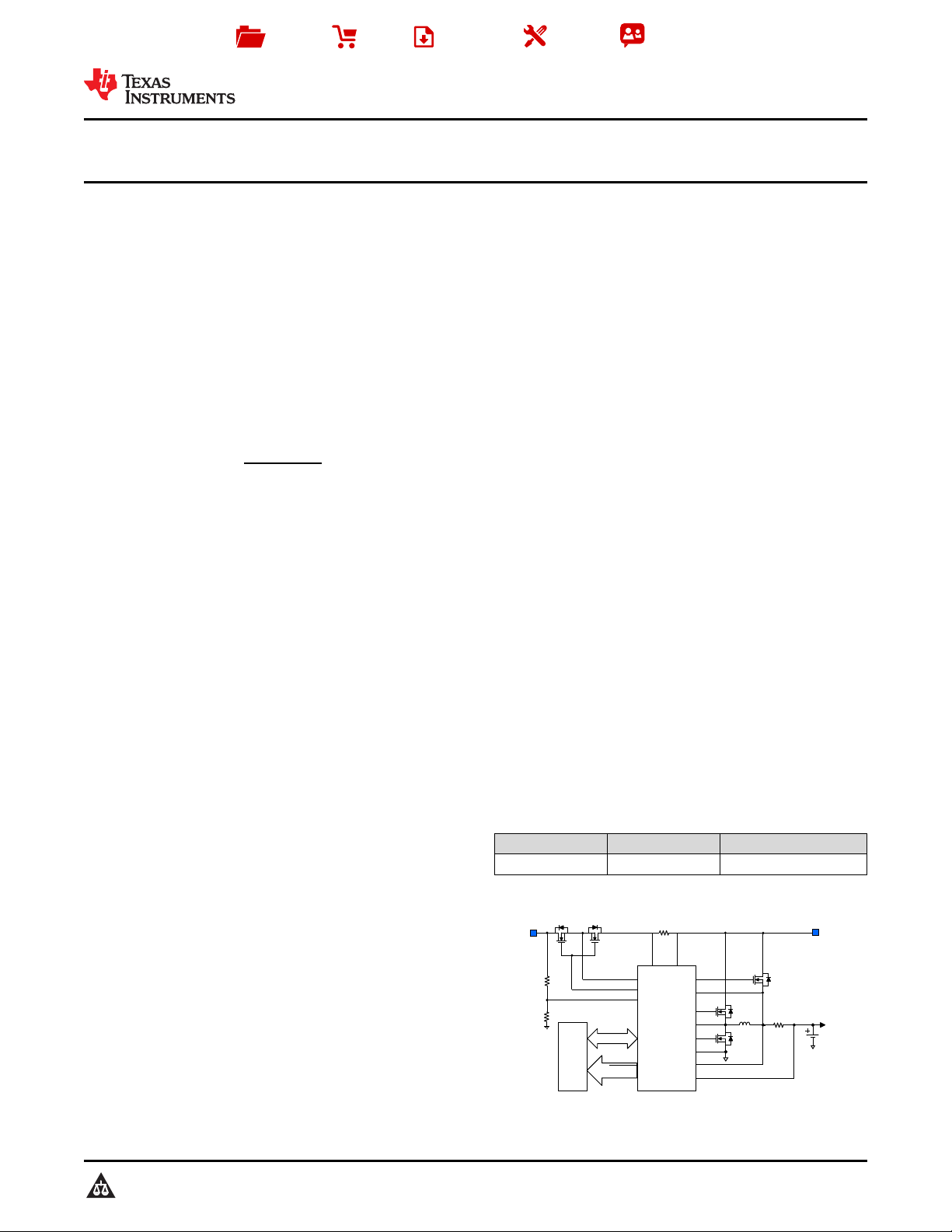
R
SR
Adapter
4.5-24V
HOST
bq24780S
Hybrid Power
Boost Charge
Controller
SYS
Battery
Pack
N-FET Driver
N-FET Driver
1S-4S
SMBus
IADP, ,PROCHOT
PMON, IDCHG
SMBus Controls V & I
with high accuracy
Adapter Detection
Enhanced Safety:
OCP,OVP, FET Short
Integration:
Loop Compensation; Soft-Start
Comparator, BTST Diode
R
AC
Product
Folder
Order
Now
Technical
Documents
Tools &
Software
Support &
Community
bq24780S
SLUSC27C –APRIL 2015–REVISED MARCH 2017
bq24780S 1- to 4-Cell Hybrid Power Boost Mode Battery Charge Controller
With Power and Processor Hot Monitoring
1 Features
1
• Industrial Innovative Charge Controller With
Hybrid Power Boost Mode
– Adapter and Battery Provides Power to
System Together for Intel®CPU Turbo Mode
– Ultra-Fast Transient Response of 150 µs to
Enter Boost Mode
– Hybrid Power Boost Mode from 4.5- to 24-V
System
– Charge 1- to 4-Cell Battery Pack from 4.5- to
24-V Adapter
• High Accuracy Power and Current Monitoring for
CPU Throttling
– Comprehensive PROCHOT Profile
– ± 2% Current Monitor Accuracy
– ± 5% System Power Monitor Accuracy
(PMON)
• Automatic NMOS Power Source Selection from
Adapter or Battery
– ACFET Fast Turn on in 100 µs
• Programmable Input Current, Charge Voltage,
Charge and Discharge Current Limit
– ±0.4% Charge Voltage (16-mV step)
– ±2% Input Current (128-mA/step)
– ±2% Charge Current (64-mA/step)
– ±2% Discharge Current (512-mA/step)
• High Integration
– Battery LEARN Function
– Battery Present Monitor
– Boost Mode Indicator
– Loop Compensation
– BTST Diode
• Enhanced Safety Features for Overvoltage
Protection, Overcurrent Protection, Battery,
Inductor, and MOSFET Short-Circuit Protection
• Switching Frequency: 600 kHz, 800 kHz, and
1 MHz
• Realtime System Control on ILIM Pin to Limit
Charge and Discharge Current
• 0.65 mA Adapter Standby Quiescent Current for
Energy Star
1
An IMPORTANT NOTICE at the end of this data sheet addresses availability, warranty, changes, use in safety-critical applications,
intellectual property matters and other important disclaimers. PRODUCTION DATA.
2 Applications
• Notebook, Ultrabook, Detachable, and Tablet PC
• Handheld Terminal
• Industrial and Medical Equipment
• Portable Equipment
3 Description
The bq24780S device is a high-efficiency,
synchronous battery charger, offering low component
count for space-constrained, multi-chemistry battery
charging applications.
The bq24780S device supports hybrid power boost
mode (previously called "turbo boost mode"). It allows
battery discharge energy to system when system
power demand is temporarily higher than adapter
maximum power level. Therefore, adapter does not
crash.
The bq24780S device uses two charge pumps to
separately drive N-channel MOSFETs (ACFET,
RBFET, and BATFET) for automatic system power
source selection.
Through SMBus, system power management
microcontroller programs input current, charge
current, discharge current, and charge voltage DACs
with high regulation accuracies.
The bq24780S device monitors adapter current
(IADP), battery discharge current (IDCHG), and
system power (PMON) for host to throttle back CPU
speed or reduce system power when needed.
The bq24780S device charges 1-, 2-, 3-, or 4-series
Li+ cells.
Device Information
PART NUMBER PACKAGE BODY SIZE (NOM)
bq24780S WQFN (28) 4.00 × 4.00 mm
(1) For all available packages, see the orderable addendum at
the end of the data sheet.
(1)
2

bq24780S
SLUSC27C –APRIL 2015–REVISED MARCH 2017
www.ti.com
Table of Contents
1 Features.................................................................. 1
2 Applications ........................................................... 1
3 Description ............................................................. 1
4 Revision History..................................................... 2
5 Pin Configuration and Functions......................... 3
6 Specifications......................................................... 5
6.1 Absolute Maximum Ratings ...................................... 5
6.2 ESD Ratings.............................................................. 5
6.3 Recommended Operating Conditions....................... 5
6.4 Thermal Information.................................................. 6
6.5 Electrical Characteristics........................................... 6
6.6 Timing Requirements.............................................. 11
6.7 Typical Characteristics............................................ 13
7 Detailed Description............................................ 14
7.1 Overview ................................................................. 14
7.2 Functional Block Diagram ....................................... 15
7.3 Feature Description................................................. 16
7.4 Device Functional Modes........................................ 22
7.5 Programming........................................................... 23
7.6 Register Maps......................................................... 25
8 Application and Implementation ........................ 36
8.1 Application Information............................................ 36
8.2 Typical Applications ................................................ 36
9 Power Supply Recommendations...................... 44
10 Layout................................................................... 44
10.1 Layout Guidelines ................................................. 44
10.2 Layout Examples................................................... 45
11 Device and Documentation Support................. 48
11.1 Receiving Notification of Documentation Updates 48
11.2 Community Resources.......................................... 48
11.3 Trademarks........................................................... 48
11.4 Electrostatic Discharge Caution............................ 48
11.5 Glossary................................................................ 48
12 Mechanical, Packaging, and Orderable
Information........................................................... 48
4 Revision History
Changes from Revision B (April 2015) to Revision C Page
• Full data sheet to product folder............................................................................................................................................. 1
Changes from Revision A (April 2015) to Revision B Page
• Changed the Description for pin 22 (GND) in the Pin Functions table................................................................................... 4
• Changed the Thermal Pad to PowerPAD in the Pin Functions table..................................................................................... 4
• Changed 16X to 20X on the SRP and SRN pins of the Functional Block Diagram ............................................................ 15
• Changed C4 From: 0.01 μF To: 0.1 μF in Figure 17 ........................................................................................................... 36
Changes from Original (April 2015) to Revision A Page
• Changed V
in the Electrical Characteristics, MIN From: 190% To: 180%, MAX From: 215% To: 220% ..................... 9
(ACOC)
• Changed "ChargeOption() bit [0] = 0" To: REG0x12[0] in Enable and Disable Charging.................................................... 17
• Changed " (REG0x12[1])" To: (REG0x12[0]=1) in Enable and Disable Charging ............................................................... 17
• Changed " REG0x12" To: "REG0x12[0]" in Battery Charging ............................................................................................ 22
• Changed Bit [10:9] in Table 9 From: 11: 8 ms To: 11: 800 µs ............................................................................................ 30
• Added sentence to Bit [7:6] in Table 9 " If REG0x15() is programmed..." ........................................................................... 30
• Changed text in Bit [5] of Table 9 From: "write 0x3C[2] = 1." To: "write 0x3C[2] = 0."........................................................ 30
• Deleted text from Bit [5] of Table 9 "This function is not available in 1s battery."................................................................ 30
2
Submit Documentation Feedback Copyright © 2015–2017, Texas Instruments Incorporated
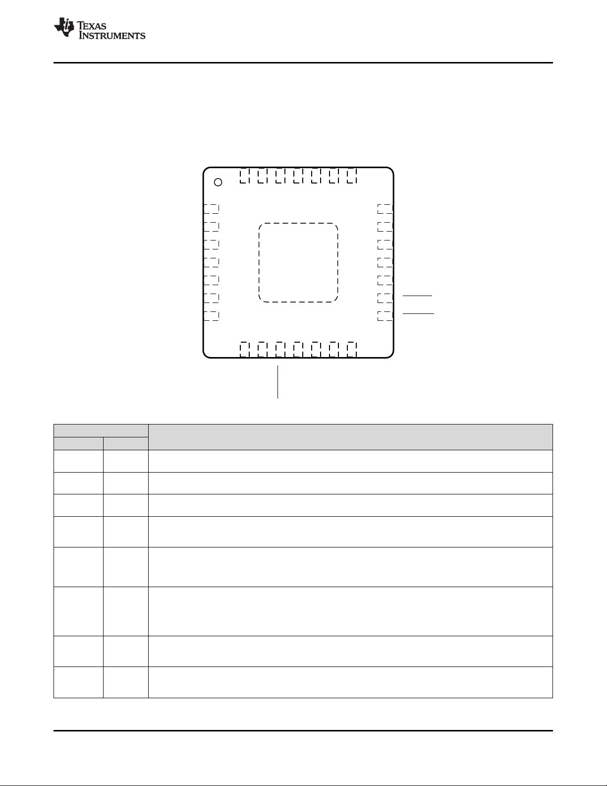
Thermal
Pad
28 VCC8IDCHG
1ACN 21 ILIM
27 PHASE9PMON
2ACP 20 SRP
26 HIDRV10PROCHOT
3CMSRC 19 SRN
25 BTST11SDA
4ACDRV 18 BATDRV
24 REGN12SCL
5ACOK 17 BATSRC
23 LODRV13CMPIN
6ACDET 16 TB_STAT
22 GND14CMPOUT
7IADP 15 BATPRES
www.ti.com
5 Pin Configuration and Functions
bq24780S
SLUSC27C –APRIL 2015–REVISED MARCH 2017
RUY Package
28-Pin WQFN
Top View
PIN
NAME NUMBER
ACN 1
ACP 2
CMSRC 3
Input current sense resistor negative input. Place an optional 0.01-µF ceramic capacitor from ACN to GND for
common-mode filtering. Place a 0.1-µF ceramic capacitor from ACN to ACP to provide differential mode filtering.
Input current sense resistor positive input. Place a 0.1-µF ceramic capacitor from ACP to GND for commonmode filtering. Place a 0.1-µF ceramic capacitor from ACN to ACP to provide differential-mode filtering.
ACDRV charge pump source input. Place a 4-kΩ resistor from CMSRC to the common source of ACFET (Q1)
and RBFET (Q2) to limit the inrush current on CMSRC pin.
Charge pump output to drive both adapter input N-channel MOSFET (ACFET) and reverse blocking N-channel
ACDRV 4
MOSFET (RBFET). ACDRV voltage is 6 V above CMSRC when ACOK is HIGH. Place a 4-kΩ resistor from
ACDRV to the gate of ACFET and RBFET limits the inrush current on ACDRV pin.
Active HIGH AC adapter detection open drain output. It is pulled HIGH to external pullup supply rail by external
ACOK 5
ACDET 6
IADP 7
IDCHG 8
pullup resistor when a valid adapter is present (ACDET above 2.4 V, VCC above UVLO but below ACOV and
VCC above BAT). If any of the above conditions is not valid, ACOK is pulled LOW by internal MOSFET. Connect
a 10-kΩ pullup resistor from ACOK to the pullup supply rail.
Adapter detection input. Program adapter valid input threshold by connecting a resistor divider from adapter
input to ACDET pin to GND pin. When ACDET pin is above 0.6 V and VCC is above UVLO, REGN LDO is
present, ACOK comparator, input current buffer (IADP), discharge current buffer (IDCHG), independent
comparator, and power monitor buffer (PMON) can be enabled with SMBus. When ACDET is above 2.4V, and
VCC is above SRN but below ACOV, ACOK goes HIGH.
Buffered adapter current output. V
The ratio of 20x and 40x is selectable with SMBus. Place 100-pF (or less) ceramic decoupling capacitor from
IADP pin to GND. This pin can be floating if this output is not in use.
Buffered discharge current. V
The ratio of 8x or 16x is selectable with SMBus. Place 100-pF (or less) ceramic decoupling capacitor from
IDSCHG pin to GND. This pin can be floating if this output is not in use.
Pin Functions
= 20 or 40 × (V
(IADP)
= 8 or 16 × (V
(IDCHG)
DESCRIPTION
– V
(ACP)
– V
(SRN)
(SRP)
(ACN)
)
)
Submit Documentation FeedbackCopyright © 2015–2017, Texas Instruments Incorporated
3
bq24780S
SLUSC27C –APRIL 2015–REVISED MARCH 2017
Pin Functions (continued)
PIN
NAME NUMBER
Buffered total system power. The output current is proportional to the total power from the adapter and battery.
PMON 9
The ratio is selectable through SMBus. Place a resistor from PMON pin to GND to generate PMON voltage.
Place a 100-pF (or less) ceramic decoupling capacitor from PMON pin to GND. This pin can be floating if this
output is not in use.
Active low, open-drain output of the processor hot indicator. The charger IC monitors events like adapter current,
PROCHOT 10
battery discharge current. After any event in the PROCHOT profile is triggered, a minimum 10-ms pulse is
asserted.
SMBus open-drain data I/O. Connect to SMBus data line from the host controller or smart battery. SMBus
SDA 11
communication starts when VCC is above UVLO. Connect a 10-kΩ pullup resistor according to SMBus
specifications.
SMBus open-drain clock input. Connect to SMBus clock line from the host controller or smart battery. SMBus
SCL 12
communication starts when VCC is above UVLO. Connect a 10-kΩ pullup resistor according to SMBus
specifications.
Input of independent comparator. Internal reference, output polarity and deglitch time is selectable by SMBus.
CMPIN 13
Place a resistor between CMPIN and CMPOUT to program hysteresis when the polarity is HIGH. If comparator
is not in use, CMPIN is tied to ground, and CMPOUT is left floating.
Open-drain output of independent comparator. Place 10-kΩ pullup resistor from CMPOUT to pullup supply rail.
CMPOUT 14
Comparator reference, output polarity and deglitch time is selectable by SMBus. If comparator is not in use,
CMPIN is tied to ground, and CMPOUT is left floating.
Active low battery present input signal. Low indicates battery present, high indicates battery absent. The device
BATPRES 15
exits the LEARN function and turns on ACFET/RBFET within 100 µs if BATPRES pin is pulled high. Upon
BATPRES from LOW to HIGH, battery charging and hybrid power boost mode are disabled. The host can
enable charging and hybrid power boost mode by write to REG0x14() and REG0x15() when BATPRES is HIGH
Active low, open-drain output for hybrid power boost mode indication. It is pulled low when the IC is operating in
TB_STAT 16
boost mode. Otherwise, it is pulled high. Connect a 10-kΩ pullup resistor from TB_STAT pin to the pullup supply
rail.
BATSRC 17 Connect to the source of N-channel BATFET. BATDRV voltage is 6 V above BATSRC to turn on BATFET.
Charge pump output to drive N-channel MOSFET between battery and system (BATFET). BATDRV voltage is
BATDRV 18
6 V above BATSRC to turn on BATFET and power system from battery. BATDRV is shorted to BATSRC to turn
off BATFET. Place a 4-kΩ resistor from BATDRV to the gate of BATFET limits the inrush current on BATDRV
pin.
Charge current sense resistor negative input. SRN pin is for battery voltage sensing as well. Connect SRN pin
SRN 19
with a 0.1-µF ceramic capacitor to GND for common-mode filtering. Connect a 0.1-µF ceramic capacitor from
SRP to SRN to provide differential mode filtering.
SRP 20
Charge current sense resistor positive input. Connect a 0.1-µF ceramic capacitor from SRP to SRN to provide
differential mode filtering.
Charge current and discharge current limit.V
V
) for discharge current. Program ILIM voltage by connecting a resistor divider from system reference 3.3-V
ILIM 21
SRP
rail to ILIM pin to GND pin. The lower of ILIM voltage and 0x14() (for charge) or 0x39 (for discharge) reference
sets actual regulation limit. The minimum voltage on ILIM to enable charge or discharge current regulation is 120
mV.
GND 22
IC ground. On PCB layout, connect to analog ground plane, and only connect to power ground plan through pad
underneath IC.
LODRV 23 Low-side power MOSFET driver output. Connect to low-side N-channel MOSFET gate.
6-V linear regulator output supplied from VCC. The LDO is active when ACDET above 0.6 V, VCC above UVLO.
REGN 24
Connect a ≥ 2.2-µF 0603 ceramic capacitor from REGN to GND. The diode between REGN and BTST is
integrated.
BTST 25
High-side power MOSFET driver power supply. Connect a 47-nF capacitor from BTST to PHASE. The diode
between REGN and BTST is integrated inside the IC.
HIDRV 26 High-side power MOSFET driver output. Connect to the high side N-channel MOSFET gate.
PHASE 27 High-side power MOSFET driver source. Connect to the source of the high-side N-channel MOSFET.
VCC 28
Input supply from adapter or battery. Use 10-Ω resistor and 1-µF capacitor to ground as a low pass filter to limit
inrush current. A diode OR is connected to VCC. It powers charger IC from input adapter and battery.
Exposed pad beneath the IC. Analog ground and power ground star-connected only at the PowerPAD plane.
PowerPAD™
Always solder the PowerPAD to the board and have vias on the PowerPAD plane connecting to analog ground
and power ground planes. It also serves as a thermal pad to dissipate the heat.
DESCRIPTION
= 20 × (V
ILIM
SRP
– V
) for charge current and V
SRN
ILIM
= 5 × (V
www.ti.com
SRN
–
4
Submit Documentation Feedback Copyright © 2015–2017, Texas Instruments Incorporated
bq24780S
www.ti.com
SLUSC27C –APRIL 2015–REVISED MARCH 2017
6 Specifications
6.1 Absolute Maximum Ratings
over operating free-air temperature range (unless otherwise noted)
SRN, SRP, ACN, ACP, CMSRC, VCC, BATSRC –0.3 30
PHASE –2 30
Voltage
Differential voltage BTST-PHASE, HIDRV-PHASE ACDRV-CMSRC, BATDRV-BATSRC –0.3 7 V
Voltage
Voltage PHASE (2% duty cycle) –4 30 V
Voltage REGN (5ms) –0.3 9 V
Maximum differential voltage SRP–SRN, ACP–ACN –0.5 +0.5 V
Junction temperature, T
Storage temperature, T
J
stg
(1) Stresses beyond those listed under absolute maximum ratings may cause permanent damage to the device. These are stress ratings
only, and functional operation of the device at these or any other conditions beyond those indicated under recommended operating
conditions is not implied. Exposure to absolute-maximum-rated conditions for extended periods may affect device reliability.
(2) All voltages are with respect to GND if not specified. Currents are positive into, negative out of the specified pin. Consult Packaging
Section of the data book for thermal limitations and considerations of packages.
ACDET, SDA, SCL, LODRV, REGN, IADP, IDCHG, PMON, ILIM, ACOK,
CMPIN, CMPOUT, BATPRES, TB_STAT
PROCHOT –0.3 5.7
BTST, HIDRV, ACDRV, BATDRV –0.3 36
LODRV (2% duty cycle) –4 7
HIDRV (2% duty cycle) –4 36
(1)(2)
MIN MAX UNIT
–0.3 7
–40 155 °C
–55 155 °C
V
V
6.2 ESD Ratings
VALUE UNIT
(1)
±2000
±500
V
(ESD)
Electrostatic discharge
Human body model (HBM), per ANSI/ESDA/JEDEC JS-001
Charged device model (CDM), per JEDEC specification JESD22-
(2)
C101
(1) JEDEC document JEP155 states that 500-V HBM allows safe manufacturing with a standard ESD control process.
(2) JEDEC document JEP157 states that 250-V CDM allows safe manufacturing with a standard ESD control process.
6.3 Recommended Operating Conditions
over operating free-air temperature range (unless otherwise noted)
MIN MAX UNIT
SRN, SRP, ACN, ACP, CMSRC, VCC, BATSRC 0 24
PHASE –2 24
Voltage
Maximum difference SRP–SRN, ACP–ACN –0.4 +0.4 V
Junction temperature, T
Operating free-air temperature, T
ACDET, SDA, SCL, LODRV, REGN, IADP, IDCHG, PMON, ILIM, ACOK,
CMPIN, CMPOUT, BATPRES, TB_STAT
PROCHOT –0.3 5
BTST, HIDRV, ACDRV, BATDRV 0 30
J
A
0 6.5
–20 125
–40 85
V
V
°C
Submit Documentation FeedbackCopyright © 2015–2017, Texas Instruments Incorporated
5
bq24780S
SLUSC27C –APRIL 2015–REVISED MARCH 2017
www.ti.com
6.4 Thermal Information
bq24780S
THERMAL METRIC
(1)
UNITRUY (WQFN)
28 PINS
R
R
R
ψ
ψ
R
θJA
θJCtop
θJB
JT
JB
θJCbot
Junction-to-ambient thermal resistance 33.3 °C/W
Junction-to-case (top) thermal resistance 29.7 °C/W
Junction-to-board thermal resistance 6.5 °C/W
Junction-to-top characterization parameter 0.3 °C/W
Junction-to-board characterization parameter 6.5 °C/W
Junction-to-case (bottom) thermal resistance 1.3 °C/W
(1) For more information about traditional and new thermal metrics, see the IC Package Thermal Metrics application report, SPRA953.
6.5 Electrical Characteristics
4.5 V ≤ V
OPERATING CONDITIONS
V
VCC(OP)
CHARGE VOLTAGE REGULATION
V
BAT(REG_RNG)
V
BAT(REG_ACC)
CHARGE CURRENT REGULATION
V
IREG(CHG_RNG)
I
CHRG(REG_ACC)
I
LGK(SRP-SRN)
≤ 24 V, –40°C ≤ TJ≤ 125°C, typical values are at TA= 25°C, with respect to GND (unless otherwise noted)
VCC
PARAMETER TEST CONDITIONS MIN TYP MAX UNIT
VCC/ACP/ACN operating voltage 4.5 24 V
Battery voltage 1.024 19.2 V
ChargeVoltage() = 0x41A0 16.8 V
–10°C-85°C –0.4% 0.4%
–40°C-125°C –0.5% 0.5%
ChargeVoltage() = 0x3130 12.592 V
–10°C-85°C –0.4% 0.4%
Charge voltage regulation accuracy
Charge current regulation differential
voltage
Charge current regulation accuracy
(SRN > 2.8 V)
SRP and SRN leakage mismatch –8 8 µA
–40°C-125°C –0.5% 0.5%
ChargeVoltage() = 0x20D0 8.4 V
–10°C-85°C –0.4% 0.4%
–40°C-125°C –0.6% 0.6%
ChargeVoltage() = 0x1060 4.192 V
–10°C-85°C –0.5% 0.8%
–40°C-125°C –0.7% 0.8%
V
ChargeCurrent() = 0x1000
ChargeCurrent() = 0x0800
ChargeCurrent() = 0x0200
ChargeCurrent() = 0x0100 256 mA
ChargeVoltage() = 0x20D0, 0x3031, 0x41A0 –16% 16%
ChargeVoltage() = 0x1060 –20% 20%
ChargeCurrent() = 0x00C0
ChargeCurrent() = 0x0080
IREG(CHG)
= V
SRP
– V
SRN
0 81.28 mV
4096 mA
–2% 2%
2048 mA
–3% 3%
512 mA
–10% 10%
192 mA
–20% 20%
128 mA
–30% 30%
6
Submit Documentation Feedback Copyright © 2015–2017, Texas Instruments Incorporated
www.ti.com
Electrical Characteristics (continued)
bq24780S
SLUSC27C –APRIL 2015–REVISED MARCH 2017
4.5 V ≤ V
≤ 24 V, –40°C ≤ TJ≤ 125°C, typical values are at TA= 25°C, with respect to GND (unless otherwise noted)
VCC
PARAMETER TEST CONDITIONS MIN TYP MAX UNIT
DISCHARGE CURRENT REGULATION
V
(IREG_CHG_RNG)
I
(DCHRG_REG_ACC)
Charge current regulation differential
voltage
Discharge current regulation accuracy
INPUT CURRENT REGULATION
V
(IREG_DPM_RNG)
I
(DPM_REG_ACC)
I
LGK(ACP-ARN)
Input current regulation differential
voltage
Input current regulation accuracy
ACP and ACN leakage mismatch –5 5 µA
INPUT CURRENT SENSE AMPLIFIER
V
(IADP)
I
(IADP)
A
(IADP)
V
(IADP_ACC)
V
(IADP_CLAMP)
C
(IADP)
IADP output voltage 0 3.3 V
IADPT output current 0 1 mA
IADP sense amplifier gain V
Current sense amplifier gain accuracy
IADP clamp voltage 3 3.3 V
IADP output load capacitance With 0 to 1mA load 100 pF
DISCHARGE CURRENT SENSE AMPLIFIER
V
(IDCHG)
I
(IDCHG)
A
(IDCHG)
V
(IDCHG_ACC)
V
(IDCHG_CLAMP)
C
(IDCHG)
IDCHG output voltage 0 3.3 V
IDCHG output current 0 1 mA
Current sense amplifier gain V
Current sense output accuracy
IDCHG clamp voltage 3 3.3 V
IDCHG output load capacitance With 0 to 1mA load 100 pF
V
IREG(IDISCHG)
= V
SRN
– V
ChargeCurrent() = 0x2000
ChargeCurrent() = 0x1000
ChargeCurrent() = 0x0800
ChargeCurrent() = 0x0400
ChargeCurrent() = 0x0400
V
(IREG_DPM)
= V
(ACP)
– V
(ACN)
InputCurrent() = 0x1000
InputCurrent() = 0x0800
InputCurrent() = 0x0400
InputCurrent() = 0x0200
/ V
(IADP)
V
(ACP-ACN)
V
(ACP-ACN)
V
(ACP-ACN)
V
(ACP-ACN)
V
(ACP-ACN)
V
(ACP-ACN)
(IDCHG)/V(SRN-SRP)
V
(SRN-SRP)
V
(SRN-SRP)
V
(SRN-SRP)
V
(SRN-SRP)
, REG0x12[4] = 0 20 V/V
(ACP-ACN)
= 40 mV –2% 2%
= 20 mV –4% 4%
≥ 10 mV –7% 7%
≥ 5 mV –20% 20%
≥ 2.5 mV –30% 30%
≥ 1.5 mV –40% 40%
, REG0x12[3] = 1 16 V/V
= 40 mV –5% 5%
= 20 mV –9% 9%
= 10 mV –17% 17%
= 5 mV –34% 34%
SRP
0 322.56 mV
8192 mA
–2% 2%
4096 mA
–3% 3%
2048 mA
–5% 5%
1024 mA
–8% 8%
512 mA
–10% 10%
0 80.64 mV
4096 mA
–2% 2%
2048 mA
–3% 3%
1024 mA
–5% 5%
512 mA
–12% 12%
Submit Documentation FeedbackCopyright © 2015–2017, Texas Instruments Incorporated
7
bq24780S
SLUSC27C –APRIL 2015–REVISED MARCH 2017
Electrical Characteristics (continued)
www.ti.com
4.5 V ≤ V
≤ 24 V, –40°C ≤ TJ≤ 125°C, typical values are at TA= 25°C, with respect to GND (unless otherwise noted)
VCC
PARAMETER TEST CONDITIONS MIN TYP MAX UNIT
SYSTEM POWER SENSE AMPLIFIER
V
(PMON)
I
(PMON)
A
(PMON)
V
PMON_ACC
V
PMON_CLAMP
C
PMON
PMON output voltage 0 3.3 V
PMON output current 0 160 µA
PMON system gain V
PMON Gain Accuracy
(REG0x3B[9]=1)
PMON clamp voltage 3% 3.3% V
Maximum output load capacitance With 0 to 1 mA 100 pF
REGN REGULATOR
V
(REGN_REG)
I
(REGN_LIM_Charging)
V
LDO(DROPOUT)
I
(REGN_LIM)
I
(REGN_TSHUT)
C
(REGN)
REGN regulator voltage V
REGN current limit when in charging
mode
REGN output voltage in dropout V
REGN current limit when not in charging
REGN output under thermal shutdown V
REGN output capacitor I
VCCUNDER VOLTAGE LOCKOUT COMPARATOR
V
VCC(UVLO)
V
VCC(UVLO_HYS)
Input undervoltage rising threshold VCCrising 2.4 2.6 2.8 V
Input undervoltage falling hysteresis 200 mV
QUIESCENT CURRENT
Current with battery only,
I
BAT
I
AC
TJ= 0 to 85°C,
I
+ I
+ I
SRP
ACN
+ I
I
SRN
ACP
Adapter current,
I
+ I
ACP
+ I
VCC
BATSRC
ACN
+ I
+ I
ACDRV
PHASE
ACOK COMPARATOR
V
(ACOK_RISE)
V
(ACOK_FALL)
V
(WAKEUP_RISE)
V
(WAKEUP_FALL)
ACOK rising threshold V
ACOK falling threshold V
WAKEUP detect rising threshold V
WAKEUP detect falling threshold V
VCC to SRN COMPARATOR (VCC_SRN)
V
(VCC-SRN_FALL)
V
(VCC-SRN _RISE)
VCC-SRN falling threshold to turn off
ACFET
VCC-SRN rising threshold to turn on
ACFET
ACN to SRN COMPARATOR (ACN_SRN)
V
(ACN-SRN_FALL)
V
(ACN- SRN _RISE)
ACN to BAT falling threshold VCC ramps
up above SRN
ACN to BAT rising threshold to turn on
BATFET
+ I
+ I
VCC
CMSRC
(PMON)
/(PIN+ P
, REG0x3B[9] = 1 1 µA/W
BAT
Adapter Only with System Power = 19.5V/45W –4% 4%
Adapter Only with System Power = 12V/24W –6% 6%
Adapter Only with System Power = 5V/9W –10% 10%
Battery Only with System Power 11V/44W –4.5% 4.5%
Battery Only with System Power 7.4V/29.8W –7% 7%
Battery Only with System Power 3.7V/14.4W –10% 10%
> V
VCC
V
(REGN)
VCC
V
REGN
mode
REGN
LOAD
V
BAT
REG0x12[15] = 1
V
BAT
REG0x12[15] = 1
+
V
BAT
BATFET on, REG0x12[15] = 0, REGN = 0 V,
, V
(UVLO)
= 0 V, V
= 5 V, I
LOAD
= 0 V, V
= 5V 13 23 mA
= 100 µA to 50 mA 2.2 μF
= 16.8 V, VCC disconnected from battery,
= 16.8 V, VCC connected from battery,
= 16.8 V, VCC connect to battery,
Comparator and PROCHOT enabled, PMON
(ACDET)
VCC
> V
(wakeup_RISE)
> V
, in charging mode 80 100 mA
(UVLO)
5.7 6 6.3 V
= 20 mA 4.4 4.6 4.75 V
> V
VCC
, Not in charging
(UVLO)
13 mA
25 44
700 800
disabled, TJ= 0 to 85°C
V
(VCC_ULVO)
charge disabled
V
(VCC_ULVO)
charge enabled, no switching
V
(VCC_ULVO)
charge enabled, switching, MOSFET Qg 4nC
VCC
VCC
VCC
VCC
> V
(VCC_UVLO)
> V
(VCC_UVLO)
> V
(VCC_UVLO)
> V
(VCC_UVLO)
< V
< V
< V
VCC
VCC
VCC
< V
< V
< V
(ACOVP)
(ACOVP)
(ACOVP)
, V
, V
, V
(ACDET)
(ACDET)
(ACDET)
> 2.4 V,
> 2.4 V,
> 2.4 V,
0.65 0.8
1.6 3
10
, ACDET ramps up 2.375 2.4 2.425 V
, ACDET ramps down 2.3 2.345 2.395 V
, ACDET ramps up 0.57 0.8 V
, ACDET ramps down 0.3 0.51 V
VCC ramps down to SRN –20 60 140 mV
VCC ramps up above SRN 170 260 360 mV
ACN ramps down towards SRN 120 200 280 mV
ACN ramps above SRN 220 290 360 mV
5
μA
mA
8
Submit Documentation Feedback Copyright © 2015–2017, Texas Instruments Incorporated
www.ti.com
Electrical Characteristics (continued)
bq24780S
SLUSC27C –APRIL 2015–REVISED MARCH 2017
4.5 V ≤ V
≤ 24 V, –40°C ≤ TJ≤ 125°C, typical values are at TA= 25°C, with respect to GND (unless otherwise noted)
VCC
PARAMETER TEST CONDITIONS MIN TYP MAX UNIT
HIGH SIDE IFAULT COMPARATOR (IFAULT_HI)
V
(ACN_PH_RISE)
ACN to PH rising threshold reg0x37 bit [7] = 0 450 750 1200 mV
LOW SIDE IFAULT COMPARATOR (IFAULT_LOW)
V
(IFAULT_LO_RISE)
PHASE to GND rising threshold reg0x37 bit [6] = 1 180 250 340 mV
INPUT OVERVOLTAGE COMPARATOR (ACOVP)
V
(ACOV)
V
(ACOV_HYS)
VCC overvoltage rising threshold VCC ramps up 24 26 28 V
VCC overvoltage falling hysteresis VCC ramps down 1 V
INPUT OVERCURRENT COMPARATOR (ACOC)
V
(ACOC)
V
(ACOC_CLAMP)
Rising threshold w.r.t. ICRIT input current
limit
ACOC threshold V
BAT OVERVOLTAGE COMPARATOR (BAT_OVP)
V
OVP(RISE)
V
OVP(FALL)
I
OVP
Overvoltage rising threshold as
percentage of V
BAT(REG)
Overvoltage falling threshold as
percentage of V
BAT(REG)
Discharge resistor on SRP
CHARGE OVERCURRENT COMPARATOR (CHG_OCP)
Cycle-by-cycle overcurrent limit,
V
OCP(limit)
measured voltage between SRP and
SRN
CHARGE UNDERCURRENT COMPARATOR (CHG_UCP)
V
UCP(FALL)
Cycle-by-cycle undercurrent falling
threshold
LIGHT LOAD COMPARATOR (LIGHT_LOAD)
V
LL(FALL)
V
LL(RISE_HYST)
Light load falling threshold SRP ramps down towards SRN 1.25 mV
Light load rising hysteresis SRP ramps above SRN 1.25 mV
BATTERY DEPLETION COMPARATOR (BAT_DEPL)
V
BAT(DEPL_FALL)
V
BAT(DEPL_RISE_ HYST)
V
BAT(DEPL_RDEG)
V
BAT(DEPL_FDEG)
Battery depletion falling threshold, as
percentage of voltage regulation limit
Battery depletion rising hysteresis
Battery depletion rising deglitch
Battery depletion falling deglitch
BATTERY LOWV COMPARATOR (BAT_LOWV)
V
BAT(LV_FALL)
V
BAT(LV_RHYST)
I
BAT(LV_RESET)
Battery LOWV falling threshold SRN ramps down 2.3 2.5 2.8 V
Battery LOWV rising hysteresis SRN ramps up 200 mV
Battery LOWV charge current limit Measure across SRP and SRN 5 mV
THERMAL SHUTDOWN COMPARATOR (TSHUT)
T
SHUT
T
SHUT(HYS)
Thermal shutdown rising temperature Temperature ramps up 155 °C
Thermal shutdown hysteresis, falling Temperature ramps down 20 °C
ILIM COMPARATOR
V
ILIM(FALL)
V
ILIM(RISE)
ILIM as converter enable falling threshold V
ILIM as converter enable rising threshold V
REG0x37[9] = 1 180% 200% 220%
(ACP)
– V
(ACN)
50 190 mV
SRN ramps up 103% 104% 106%
SRN ramps down 102%
VSRN > 6 V 6
VSRN = 4.5 V 2.5
mA
ChargeCurrent() = 0x0xxxH 54 60 66 mV
ChargeCurrent() = 0x1000H – 0x17C0H 80 90 100 mV
ChargeCurrent() = 0x1800H – 0x1FC0H 110 120 130 mV
SRP ramps down towards SRN 1 5 9 mV
REG0x3B[15:14] = 00 56% 60% 64%
REG0x3B[15:14] = 01 60% 64% 68%
REG0x3B[15:14] = 10 64% 68% 72%
REG0x3B[15:14] = 11 68% 72% 78%
REG0x3B[15:14] = 00 225 305 400
REG0x3B[15:14] = 01 240 325 430
REG0x3B[15:14] = 10 255 345 450
mV
REG0x3B[15:14] = 11 280 370 490
Delay to turn on BATFET and turn off ACFET
during LEARN cycle
Delay to turn off BATFET and turn on ACFET
during LEARN cycle
falling 60 75 90 mV
ILIM
rising 90 105 120 mV
ILIM
600 ms
10 µs
Submit Documentation FeedbackCopyright © 2015–2017, Texas Instruments Incorporated
9
bq24780S
SLUSC27C –APRIL 2015–REVISED MARCH 2017
Electrical Characteristics (continued)
www.ti.com
4.5 V ≤ V
≤ 24 V, –40°C ≤ TJ≤ 125°C, typical values are at TA= 25°C, with respect to GND (unless otherwise noted)
VCC
PARAMETER TEST CONDITIONS MIN TYP MAX UNIT
INDEPENDENT COMPARATOR
V
(CMPOS)
V
(CMPCM)
V
(CMPREF)
V
(CMPRISE)
Comparator input offset –4 4 mV
Comparator input common-mode 0 6.5 V
Comparator reference voltage (CMPIN
falling)
Comparator reference hysteresis REG0x3B[6] = 0 100 mV
PWM OSCILLATOR
F
SW
PWM switching frequency
BATFET GATE DRIVER (BATDRV)
I
BAT(FET)
BATDRV charge pump current limit V
Gate drive voltage on BATFET V
R
BAT(DRV_OFF)
R
BAT(DRV_LOAD)
BATDRV turn-off resistance 5 6.2 7.4 kΩ
Minimum Load between gate and source 500 kΩ
ACFET GATE DRIVER (ACDRV)
I
(ACFET)
ACDRV charge pump current limit V
Gate drive voltage on ACFET V
R
(ACDRV_OFF)
R
(ACDRV_LOAD)
ACDRV turn-off resistance 5 6.2 7.4 kΩ
Minimum load between gate and source 500 kΩ
PWM HIGH SIDE DRIVER (HIDRV)
R
DS(HI_ON)
R
DS(HI_OFF)
V
(BTST_REFRESH)
High-side driver (HSD) turn-on resistance V
High-side driver (HSD) turn-off
Resistance
Bootstrap refresh comparator threshold
voltage
PWM LOW SIDE DRIVER (LODRV)
R
DS(LO_ON)
R
DS(LO_OFF)
Low-side driver (LSD) turn-on resistance 7.5 12 Ω
Low-side driver (LSD) turn-off resistance 0.75 1.25 Ω
INTERNAL SOFT START
I
STEP
t
STEP
Soft start step size 64 mA
Soft start step time 400 µs
PROCHOT
V
(ICRIT)
V
(INOM)
V
(IDCHG)
V
(VSYS)
ICRIT comparator threshold
INOM comparator threshold
IDCHG comparator threshold
VSYS comparator threshold REG0x3C[7:6] = 01 5.88 6 6.12 V
LOGIC INPUT (SDA, SCL, BATPRES)
V
IN(LO)
V
IN(HI)
V
IN(LEAK)
Input low threshold 0.8 V
Input high threshold 2.1 V
Input bias current V = 7 V –1 µA
LOGIC OUTPUT OPEN DRAIN (ACOK, SDA, CMPOUT, TB_STAT)
V
O(LO)
V
O(LEAK)
Output saturation voltage 5-mA drain current 500 mV
Leakage current V = 7 V –1 1 µA
LOGIC OUTPUT OPEN DRAIN (PROCHOT)
V
O(LEAK_PROCHOT)
Output saturation voltage 17-mA drain current 300 mV
Leakage current V = 5.5 V –1 1 µA
REG0x3B[7] = 0 2.28 2.3 2.32 V
REG0x3B[7] = 1 1.18 1.2 1.22 V
REG0x12[9:8] = 00 510 600 690
kHzREG0x12[9:8] = 01 680 800 920
REG0x12[9:8] = 10 850 1000 1150
– V
BAT(DRV)
– V
BAT(DRV)
– V
(ACDRV)
– V
(ACDRV)
– V
(BTST)
(PH)
V
– V
(BTST)
(PH)
V
– V
(BTST)
requested
(PH)
REG0x3C[15:11] = 01001, as percentage of
input current limit, InputCurrent() = 0x1000
as percentage of input current limit,
InputCurrent()=0x0800
REG0x3D[15:11] = 10000, as voltage between
SRN and SRP
REG0x3D[15:11] = 00100, as voltage between
SRN and SRP
= 5 V 40 60 µA
BAT(SRC)
when V
BAT(SRC)
= 5 V 40 60 µA
(CMSRC)
when V
(CMSRC)
VCC
(SRN)
> V
> V
(UVLO)
BAT(UVLO)
5.5 6.1 6.8 V
5.5 6.1 6.8 V
= 5.5 V 6 10 Ω
= 5.5 V 0.9 1.4 Ω
when low side refresh pulse is
3.85 4.3 4.7 V
147% 150% 153%
107% 110% 112%
160 163.84 167
38 40.96 44
mV
10
Submit Documentation Feedback Copyright © 2015–2017, Texas Instruments Incorporated
bq24780S
www.ti.com
SLUSC27C –APRIL 2015–REVISED MARCH 2017
6.6 Timing Requirements
4.5 V ≤ V
ACOK COMPARATOR
t
ACOK_RISE_DEG
t
ACOK_FALL_DEG
INPUT OVERCURRENT COMPARATOR (ACOC)
t
ACOC_DEG
SMBus TIMING CHARACTERISTICS
t
R
t
F
t
W(H)
t
W(L)
t
SU(STA)
t
H(STA)
t
SU(DAT)
t
H(DAT)
t
SU(STOP)
t
(BUF)
F
S(CL)
HOST COMMUNICATION FAILURE
t
timeout
t
BOOT
t
WDI
WDI
t
WDI
PWM DRIVER TIMING
t
DEADTIME_RISE
t
DEADTIME_FALL
(1) Devices participating in a transfer timeout when any clock low exceeds the 25-ms minimum timeout period. Devices that have detected
a timeout condition must reset the communication no later than the 35-ms maximum timeout period. Both a master and a slave must
adhere to the maximum value specified because it incorporates the cumulative stretch limit for both a master (10 ms) and a slave (25
ms).
(2) User can adjust threshold through SMBus ChargeOption() REG0x12.
≤ 24 V, –40°C ≤ TJ≤ 125°C, typical values are at TA= 25°C, with respect to GND (unless otherwise noted)
VCC
PARAMETER MIN TYP MAX UNIT
ACOK rising deglitch to turn on
ACFET; V
ACOK falling deglitch to turn off
ACFET
ACDET
[GBD]
> 2.4V
[GBD]
> V
VCC
1st time or REG0x12[12] = 0
V
> V
VCC
Not 1st time or REG0x12[12] = 1
V
> V
VCC
, ACDET ramps up,
VCC_UVLO
, ACDET ramps up,
VCC_UVLO
, ACDET ramps down 3 µs
VCC_UVLO
100 150 200 ms
0.9 1.3 1.7 s
V
Deglitch time to latch off ACFET 9 12 15 ms
SCLK/SDATA rise time 1 µs
SCLK/SDATA fall time 300 ns
SCLK pulse width high 4 50 µs
SCLK pulse width low 4.7 µs
Setup time for start condition 4.7 µs
Start condition hold time after which first clock pulse is generated 4 µs
Data setup time 250 ns
Data hold time 300 ns
Setup time for stop condition 4 µs
Bus free time between start and stop condition 4.7 µs
Clock frequency 10 100 kHz
SMBus bus release timeout
(1)
25 35 ms
Deglitch for watchdog reset signal 10 ms
Watchdog timeout period, REG0x12 [14:13] = 01
Watchdog timeout period, REG0x12 [14:13] = 10
Watchdog timeout period, REG0x12 [14:13] = 11
(2)
(2)
(2)
(default) 140 175 210
4 5 6
70 88 105
Driver dead time from low side to high side 20 ns
Driver dead time from high side to low side 20 ns
st
Submit Documentation FeedbackCopyright © 2015–2017, Texas Instruments Incorporated
11
bq24780S
SLUSC27C –APRIL 2015–REVISED MARCH 2017
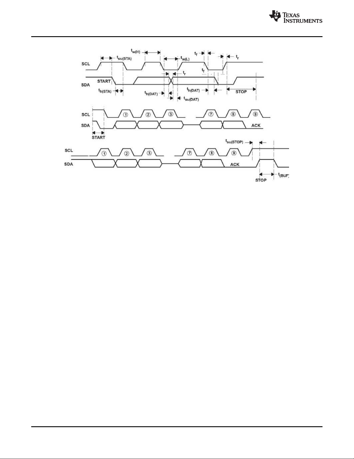
Figure 1. SMBus Communication Timing Waveforms
www.ti.com
12
Submit Documentation Feedback Copyright © 2015–2017, Texas Instruments Incorporated
Charge Current (A)
Efficiency
0 1 2 3 4 5 6 7 8
88%
90%
92%
94%
96%
98%
100%
D003
V
BAT
= 3.7 V
Discharge Current (A)
Efficiency
0 2 4 6 8 10
60%
65%
70%
75%
80%
85%
90%
95%
100%
D004
V
BAT
= 3.7 V
V
BAT
= 7.4 V
V
BAT
= 11.1 V
V
BAT
= 14.8 V
Charge Current (A)
Efficiency
0 1 2 3 4 5 6 7 8
88%
90%
92%
94%
96%
98%
100%
D001
V
BAT
= 14.8 V
V
BAT
= 11.1 V
V
BAT
= 7.4 V
Charge Current (A)
Efficiency
0 1 2 3 4 5 6 7 8
88%
90%
92%
94%
96%
98%
100%
D002
V
BAT
= 3.7 V
V
BAT
= 7.4 V
www.ti.com
6.7 Typical Characteristics
bq24780S
SLUSC27C –APRIL 2015–REVISED MARCH 2017
VIN = 20 V
Figure 2. Efficiency During Charging
VIN = 5 V
Figure 4. Efficiency During Charging
VIN = 12 V
Figure 3. Efficiency During Charging
VIN = 20 V
Figure 5. Efficiency During Boost
Submit Documentation FeedbackCopyright © 2015–2017, Texas Instruments Incorporated
13

bq24780S
SLUSC27C –APRIL 2015–REVISED MARCH 2017
www.ti.com
7 Detailed Description
7.1 Overview
The bq24780S is a 1-4 cell battery charge controller with power selection for space-constrained, multi-chemistry
portable applications such as notebook and detachable ultrabook. It supports wide input range of input sources
from 4.5 V to 24 V, and 1-4 cell battery for a versatile solution.
The bq24780S supports automatic system power source selection with separate drivers for n-channel MOSFETS
on the adapter side and battery side.
The bq24780S features Dynamic Power Management (DPM) to limit the input power and avoid AC adapter overloading. During battery charging, as the system power increases, the charging current will reduce to maintain
total input current below adapter rating. If system power demand is temporarily exceeds adapter rating, the
bq24780S supports hybrid power boost mode (previously called "turbo boost mode") to allow battery discharge
energy to supplement system power. For details of hybrid power boost mode, refer to Device Functional Modes
section.
The bq24780S closely monitors system power (PMON), input current (IADP) and battery discharge current
(IDCHG) with highly accurate current sense amplifiers. If current is too high, adapter or battery is removed, a
PROCHOT signal is asserted to CPU so that the CPU optimizes its performance to the power available to the
system.
The SMBus controls input current, charge current and charge voltage registers with high resolution, high
accuracy regulation limits. It also sets the PROCHOT timing and threshold profile to meet system requirements.
14
Submit Documentation Feedback Copyright © 2015–2017, Texas Instruments Incorporated
150ms/1.3sec
Rising Deglitch**
20X**
16X
SELECTOR
LOGIC
ACDRV
CHARGE
PUMP
REGN
LDO
SMBUS Interface
ChargeOption()
ChargeCurrent()
ChargeVoltage()
InputCurrent()
DischargeCurrent()
ManufactureID()
DeviceID()
UVLO*
3.2V
WAKEUP*
EN_REGN
ACOVP
0.6V
26V
2.4V
ACGOOD
VCC_SRN
ACOK_DRV
VREF_IAC
VREF_ICHG
ILIM
EN_CHRG
BATOVP
6mA
DAC_VALID
CHARGE_INHIBIT
EN_LEARN
VREF_VREG
VREF_ICHG
VREF_IAC
VREF_IDCHG
EN_BOOST
EN_DPM
10uA
200mV
RAMP
Frequency**
FBO
EAI EAO
PWM
ACOK_DRV
ACDRV
CMSRC+5.9V
ACDRV_CMSRC
ACOC
ACGOOD
CHARGE_INHIBIT
DAC_VALID
EN_LEARN
WATCHDOG
TIMER 175s**
WD_TIMEOUT
EN_CHRG
TYPE III
COMPENSATION
Tj
155C
TSHUT
CHG_OCP
SRP-SRN
120mV
CHG_UCP
5mV
SRP-SRN
LIGHT_LOAD
1.25mV
SRP-SRN
ACOC
ACP_ACN
2x ICRIT*
REFRESH
4.3V
BTST_PH
BATOVP
SRN
104%VREF_VREG
BATLOWV
2.5V
SRN
VCC_SRN
VCC
SRN+275mV
WAKEUP
FAST_DPM
ACP-ACN
107%xVREF_IAC
FET_LATCHOFF_EN
EN_LEARN
EN_REGN
EN_SHIP
FET_LATCHOFF_EN
VCC
ACDET
ACOK
ACP
ACN
IADP
SRP
SRN
SDA
SCL
GND
LODRV
REGN
PHASE
HIDRV
BTST
BATDRV
CMSRC
ACDRV
VREF_VREG
bq24780S
*Threshold is adjustable by registers
28
6
5
2
1
7
20
19
9
22
23
24
27
26
25
18
3
4
PWM
DRIVER
LOGIC
EN_DPM
IDCHG
PMON
BATPRES
15
PROC
HOT
detect
PROCHOT
10
IADPT
IDCHG
VSYS
8
11
12
CMPIN
13
CMPOUT
14
IREF_CMP**
VCC
(ACP-ACN)
BAT
(SRN-SRP)
EN_BOOST
17
BATSRC
BATDRV
CHARGE
PUMP
16
TB_STAT
5X
VREF_IDCHG
ACN
SRN+200mV
ILIM
21
CHG/
DCHG_EN
ILIM
120mV
1X
16X/5
www.ti.com
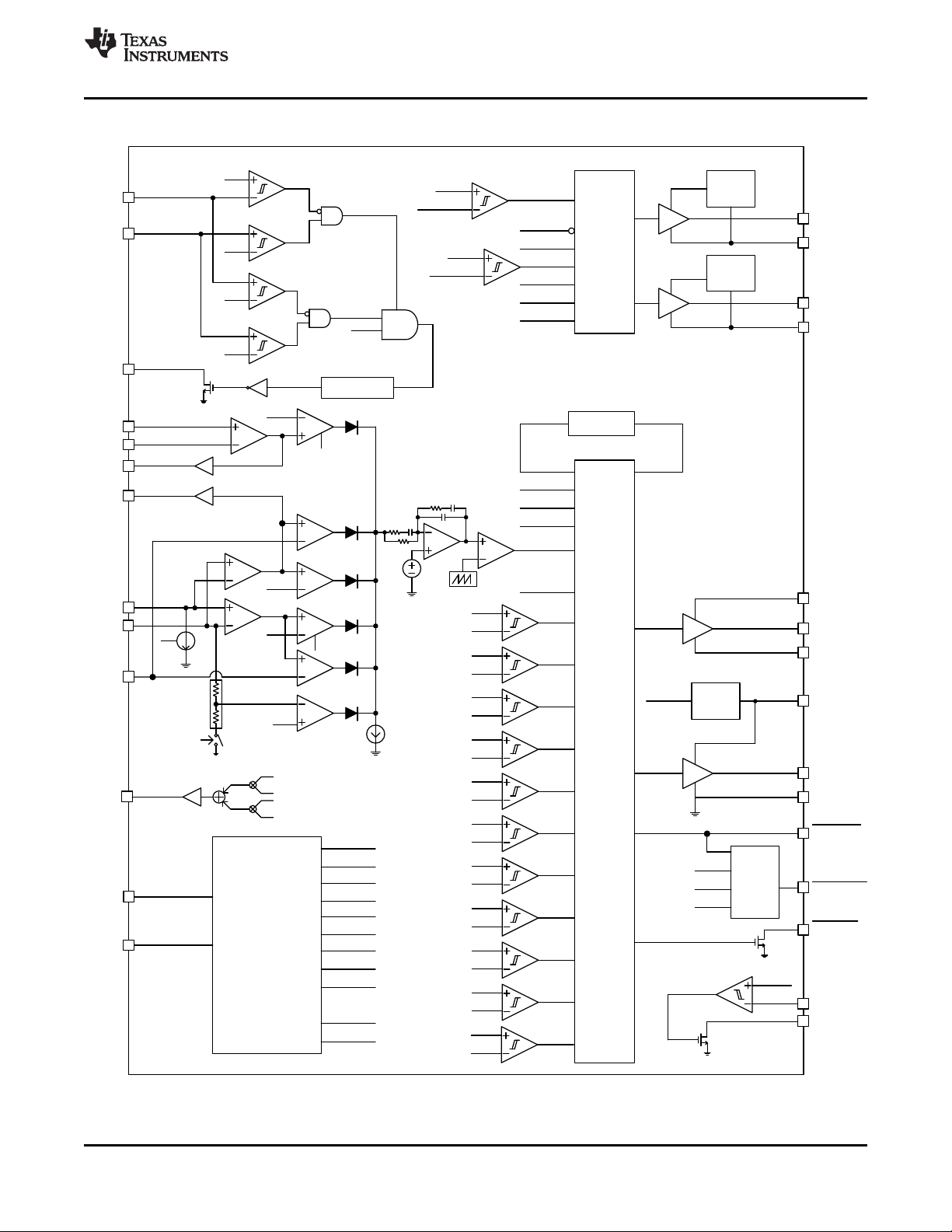
7.2 Functional Block Diagram
bq24780S
SLUSC27C –APRIL 2015–REVISED MARCH 2017
Submit Documentation FeedbackCopyright © 2015–2017, Texas Instruments Incorporated
15

bq24780S
SLUSC27C –APRIL 2015–REVISED MARCH 2017
www.ti.com
7.3 Feature Description
7.3.1 Device Power Up
The bq24780S gets power from adapter or battery. After VCC is above its UVLO threshold, the device wakes up
and starts communication.
7.3.1.1 Battery Only
When VCC voltage is above UVLO, bq24780S powers up to turn on BATFET and starts SMBus communication.
By default, bq24780S stays in low power mode (REG0x12[15] = 1) with lowest quiescent current. When
REG0x12[15] is set to 0, the device enters performance mode. User can enable IDCHG buffer, PMON,
PROCHOT or comparator through SMBus. REGN LDO is enabled (except for IDCHG buffer) for accurate
reference.
7.3.1.2 Adapter Detect and ACOK Output
An external resistor divider attenuates the adapter voltage before it goes to ACDET. The adapter detect
threshold should typically be programmed to a value greater than the maximum battery voltage, but lower than
the maximum allowed adapter voltage. When ACDET is above 0.6V, all bias circuits are enabled.
The open drain ACOK output can be pulled to external rail under the following conditions:
• V
VCC_UVLOZ
• V
ACDET
• V
VCC
The REG0x37[11] tracks the status of ACOK pin. ACOK deglitch time is 150ms at the first time adapter plug-in,
and 1.3 sec at the following plug-ins after VCC or SRN is above its UVLOZ.
> 2.4 V
– V
SRN
< V
VCC
> V
VCC_SRN_FALL
< ACOVP
+ V
VCC_SRN_HYST
7.3.1.2.1 Adapter Overvoltage (ACOVP)
When the VCC pin voltage is higher than 26 V, it is considered adapter over voltage. ACOK is pulled low, and
charge is disabled. ACFET/RBFET are turned off to disconnect the high voltage adapter to system during
ACOVP. BATFET is turned on if turn-on conditions are valid.
When VCC voltage falls below 24 V, it is considered as adapter voltage returns back to normal voltage. ACOK is
pulled high by an external pullup resistor. BATFET is turned off and ACFET and RBFET is turned on to power
the system from the adapter.
7.3.2 System Power Selection
The bq24780S device automatically switches adapter or battery power to system. An automatic break-beforemake logic prevents shoot-through currents when the selectors switch.
The ACDRV drives a pair of common-source (CMSRC) N-channel power MOSFETs (ACFET and RBFET)
between adapter and ACP. The ACFET separates adapter from system and battery, and provides a limited di/dt
when plugging in adapter by controlling the ACFET turn-on time. Meanwhile, it protects the adapter when the
system or battery is shorted. The RBFET provides negative input voltage protection and battery discharge
protection when adapter is shorted to ground, and minimizes system power dissipation with its low R
DS(on)
compared to a Schottky diode.
When the adapter is not present, ACDRV is pulled to CMSRC to keep ACFET and RBFET off, disconnecting the
adapter from the system. BATDRV stays at V
BATSRC
+ 6 V to connect battery to system if all of the following
conditions are valid:
• VCC> V
• V
ACN
< V
UVLO
SRN
+ 200 mV
• ACFET/RBFET off
After the adapter plugs in, the system power source switches from battery to adapter if all of the following
conditions are valid:
• ACOK high
• Not in LEARN mode
• In LEARN mode and V
< battery depletion threshold
SRN
16
Submit Documentation Feedback Copyright © 2015–2017, Texas Instruments Incorporated

www.ti.com
Feature Description (continued)
bq24780S
SLUSC27C –APRIL 2015–REVISED MARCH 2017
The gate drive voltage on ACFET and RBFET is V
+ 6 V. If the ACFET/RBFET have been turned on for 20
CMSRC
ms, and the voltage across gate and source is still less than 5.7 V, ACFET and RBFET are turned off. After 1.3s
delay, it resumes turning on ACFET and RBFET. If such a failure is detected seven times within 90 seconds,
ACFET/RBFET are latched off and an adapter removal and system shut down is required to force ACDET < 0.6
V to reset the IC. After IC reset from latch off, ACFET/RBFET can be turned on again. After 90 seconds, the
failure counter is reset to zero to prevent latch off.
To turn off ACFET/RBFET, one of the following conditions must be valid:
• In LEARN mode and V
is above battery depletion threshold;
SRN
• ACOK low
To limit the adapter inrush current during ACFET turn-on, the Cgs and Cgd external capacitor of ACFET must be
carefully selected following the guidelines below:
• Minimize total capacitance on system
• Cgs should be 40× or higher than Cgd to avoid ACFET false turn on during adapter hot plug-in
• Fully turn on ACFET within 20 ms, otherwise, charger IC will consider turn-on failure
• Check with MOSFET vendor on peak current rating
• Place 4-kΩ resistor in series with ACDRV, CMSRC, and BATDRV pin to limit inrush current.
7.3.3 Enable and Disable Charging
In charge mode, the following conditions have to be valid to start charge:
• Charge is enabled through SMBus (REG0x12[0], default is 0, charge enabled)
• ILIM pin voltage is higher than 120 mV
• All ChargeCurrent(), ChargeVoltage() and InputCurrent() registers have valid value programmed
• ACOK is valid (see Device Power Up for details)
• ACFET and RBFET turn on and gate voltage is high enough (see System Power Selection for details)
• V
does not exceed BATOVP threshold
SRN
• IC temperature does not exceed TSHUT threshold
• Not in ACOC condition (see Device Protections Features for details)
One of the following conditions stops on-going charging:
• Charge is inhibited through SMBus(REG0x12[0]=1)
• ILIM pin voltage is lower than 60 mV
• One of three registers is set to 0 or out of range
• ACOK is pulled low (see Device Power Up for details)
• ACFET turns off
• V
exceeds BATOVP threshold
SRN
• TSHUT IC temperature threshold is reached
• ACOC is detected (see Device Protections Features for details)
• Short circuit is detected (see Inductor Short, MOSFET Short Protection for details)
• Watchdog timer expires if watchdog timer is enabled (see Charger Timeout for details)
7.3.3.1 Automatic Internal Soft-Start Charger Current
Every time the charge is enabled, the charger automatically applies soft-start on charge current to avoid any
overshoot or stress on the output capacitors or the power converter. The charge current starts at 128 mA, and
the step size is 64 mA in CCM mode for a 10 mΩ current sensing resistor. Each step lasts around 400 μs in
CCM mode, till it reaches the programmed charge current limit. No external components are needed for this
function.
During DCM mode, the soft start up current step size is larger and each step lasts for longer time period due to
the intrinsic slow response of DCM mode.
Submit Documentation FeedbackCopyright © 2015–2017, Texas Instruments Incorporated
17
 Loading...