

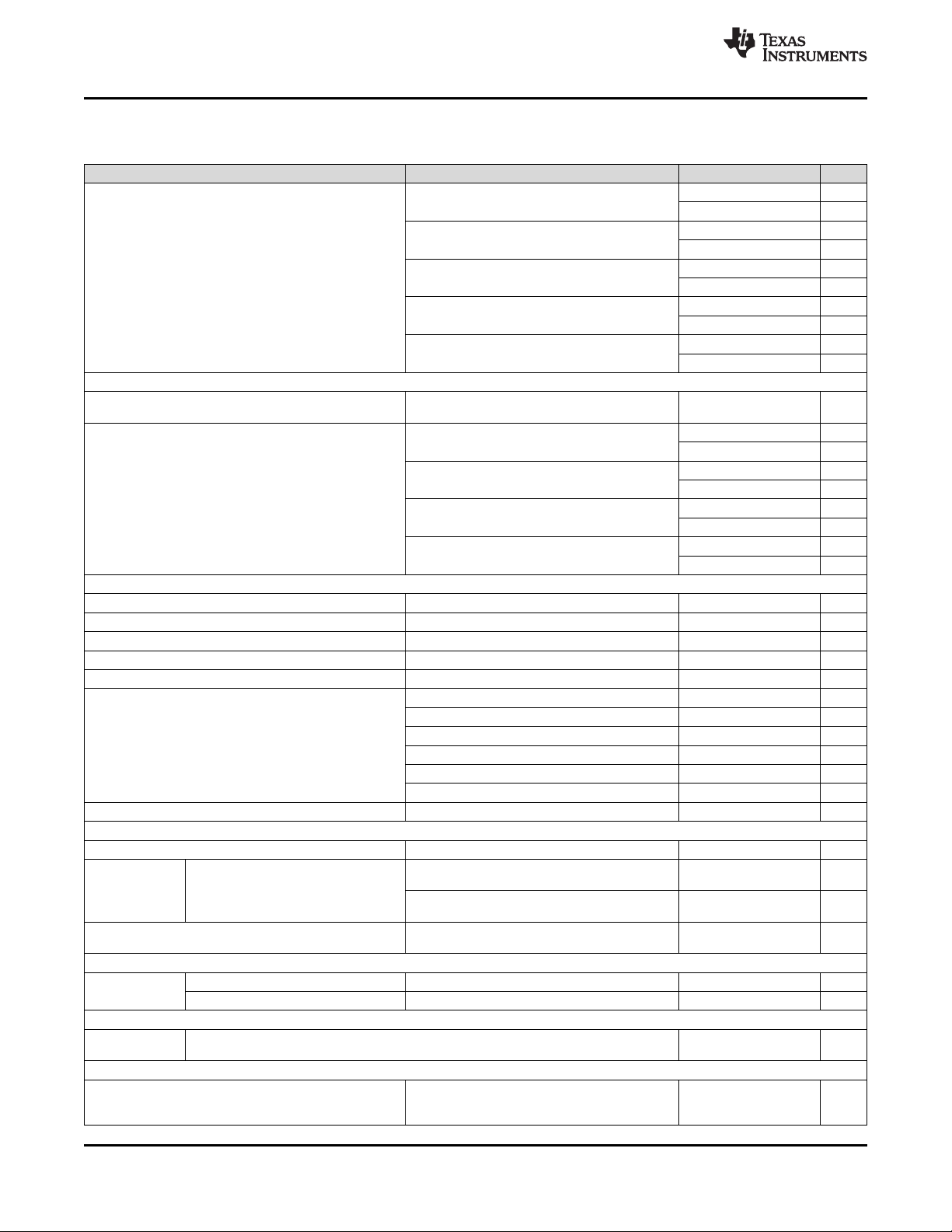
R
SR
Adapter
4.5 to 24 V
HOST
bq24735
Hybrid Power
Boost Charge
Controller
SYS
Battery
Pack
N-FET Driver
N-FET Driver
1S-4S
SMBus
SMBus Controls V and I
with high accuracy
Adapter Detection
Enhanced Safety:
OCP, OVP,
Integration: Loop Compensation;
Soft-Start Comparator
R
AC
FET Short
Product
Folder
Sample &
Buy
Technical
Documents
Tools &
Software
Support &
Community
SLUSAK9B –SEPTEMBER 2011–REVISED APRIL 2015
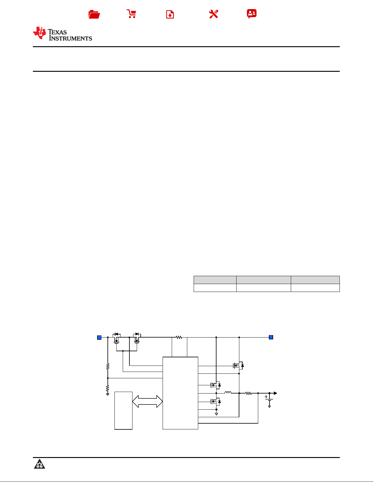
bq24735 1- to 4-Cell Li+ Battery SMBus Charge Controller for Supporting Turbo
Boost Mode With N-Channel Power MOSFET Selector
1 Features 2 Applications
1
• Adapter and Battery Provide Power to System
Together to Support Intel®CPU Turbo Boost Notebooks, and Netbooks
Mode
• SMBus Host-Controlled NMOS-NMOS
Synchronous Buck Converter With Programmable
615-, 750-, and 885-kHz Switching Frequencies
• Automatic N-Channel MOSFET Selection of
System Power Source From Adapter or Battery
Driven by Internal Charge Pumps
• Enhanced Safety Features for Overvoltage
Protection, Overcurrent Protection, Battery,
Inductor and MOSFET Short-Circuit Protection
• Programmable Input Current, Charge Voltage,
Charge Current Limits
– ±0.5% Charge Voltage Accuracy up to 19.2 V
– ±3% Charge Current Accuracy up to 8.128 A
– ±3% Input Current Accuracy up to 8.064 A
– ±2% 20× Adapter Current or Charge Current
Amplifier Output Accuracy
• Programmable Battery Depletion Threshold, and
Battery LEARN Function
• Programmable Adapter Detection and Indicator
• Integrated Loop Compensation and Soft Start
• Real-Time System Control on ILIM Pin to Limit
Charge Current
• AC Adapter Operating Range: 4.5 V to 24 V
• 5-µA Off-State Battery Discharge Current
• 0.65 mA (0.8 mA Max) Adapter Standby
Quiescent Current
• Portable Notebook Computers, UMPC, Ultra-Thin
• Handheld Terminals
• Industrial and Medical Equipment
• Portable Equipment
3 Description
The bq24735 device is a high-efficiency, synchronous
battery charger, offering low component count for
space-constrained, multichemistry battery charging
applications. The bq24735 device supports turbo
boost by allowing battery discharge energy to the
system when system power demand is temporarily
higher than the adapter maximum power level so the
adapter will not crash.
The bq24735 device uses two charge pumps to
separately drive N-channel MOSFETs (ACFET,
RBFET, and BATFET) for automatic system power
source selection.
SMBus controlled input current, charge current, and
charge voltage digital-to-analog converters (DACs)
allow for very high-regulation accuracies that can be
easily programmed by the system power
management microcontroller.
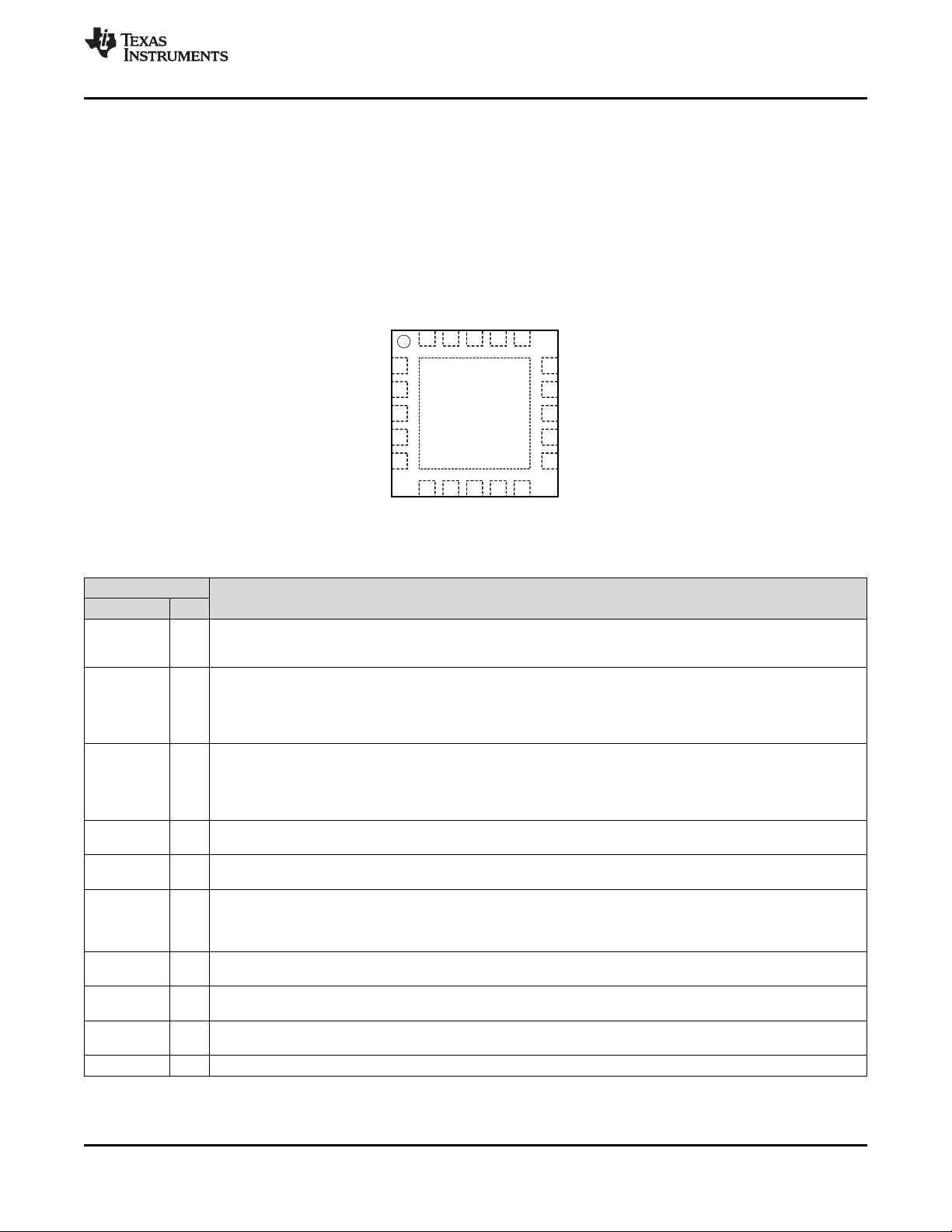
Device Information
PART NUMBER PACKAGE BODY SIZE (NOM)
bq24735 VQFN (20) 3.50 mm × 3.50 mm
(1) For all available packages, see the orderable addendum at
the end of the data sheet.
bq24735
(1)
Simplified Application Diagram
1
An IMPORTANT NOTICE at the end of this data sheet addresses availability, warranty, changes, use in safety-critical applications,
intellectual property matters and other important disclaimers. PRODUCTION DATA.

bq24735
SLUSAK9B –SEPTEMBER 2011–REVISED APRIL 2015
www.ti.com
Table of Contents
1 Features.................................................................. 1
2 Applications ........................................................... 1
3 Description ............................................................. 1
4 Revision History..................................................... 2
5 Description (continued)......................................... 3
6 Pin Configuration and Functions ......................... 3
7 Specifications......................................................... 4
7.1 Absolute Maximum Ratings...................................... 4
7.2 ESD Ratings.............................................................. 5
7.3 Recommended Operating Conditions....................... 5
7.4 Thermal Information ................................................. 5
7.5 Electrical Characteristics........................................... 5
7.6 Timing Requirements................................................ 9
7.7 Typical Characteristics............................................ 10
8 Parameter Measurement Information ................ 12
9 Detailed Description ............................................ 13
9.1 Overview ................................................................. 13
9.2 Functional Block Diagram....................................... 14
9.3 Feature Description................................................. 15
9.4 Device Functional Modes........................................ 18
9.5 Programming........................................................... 19
9.6 Register Maps......................................................... 22
10 Application and Implementation........................ 27
10.1 Application Information.......................................... 27
10.2 Typical Application ............................................... 27
10.3 System Examples ................................................. 33
11 Power Supply Recommendations ..................... 35
12 Layout................................................................... 35
12.1 Layout Guidelines ................................................. 35
12.2 Layout Example .................................................... 37
13 Device and Documentation Support ................. 38
13.1 Device Support...................................................... 38
13.2 Documentation Support ....................................... 38
13.3 Trademarks........................................................... 38
13.4 Electrostatic Discharge Caution............................ 38
13.5 Glossary................................................................ 38
14 Mechanical, Packaging, and Orderable
Information........................................................... 38
4 Revision History
NOTE: Page numbers for previous revisions may differ from page numbers in the current version.
Changes from Revision A (January 2013) to Revision B Page
• Added ESD Ratings table, Overview, Feature Description section, Device Functional Modes, Application and
Implementation section, Power Supply Recommendations section, Layout section, Device and Documentation
Support section, and Mechanical, Packaging, and Orderable Information section................................................................ 1
• Changed the format to the new template .............................................................................................................................. 1
• Deleted ", and is available in a 20-pin, 3.5x3.5 mm2QFN package" from last paragraph in Description section.
Added the Device Information table on page 1. .................................................................................................................... 3
• Added LODRV, HIDRV, and PHASE (2% duty cycle) to the Absolute Maximum Ratings table ........................................... 4
Changes from Original (September 2011) to Revision A Page
• Added V
specs ................................................................................................................................................................ 5
(ESD)
2 Submit Documentation Feedback Copyright © 2011–2015, Texas Instruments Incorporated
Product Folder Links: bq24735
1
2
3
4
5
6 7 8 9 10
15
14
13
12
11
20 19 18 17 16
ACN
ACP
CMSRC
ACDRV
ACOK
ACDET
IOUT
SDA
SCL
ILIM
BATDRV
SRN
SRP
GND
LODRV
REGN
BTST
HIDRV
PHASE
VCC
bq24735
bq24735
www.ti.com
SLUSAK9B –SEPTEMBER 2011–REVISED APRIL 2015
5 Description (continued)
The bq24735 device uses an internal input current register or an external ILIM pin to throttle down PWM
modulation to reduce the charge current. The bq24735 device charges 1-, 2-, 3-, or 4-series Li+ cells.
6 Pin Configuration and Functions
RGR Package
20-Pin VQFN
Top View
Pin Functions
PIN
NAME NO.
Adapter detection input. Program adapter valid input threshold by connecting a resistor divider from adapter input to
ACDET 6 ACDET pin to GND pin. When ACDET pin is above 0.6 V and VCC is above UVLO, REGN LDO is present, ACOK
comparator and IOUT are both active.
Charge pump output to drive both adapter input N-channel MOSFET (ACFET) and reverse blocking N-channel
MOSFET (RBFET). ACDRV voltage is 6 V above CMSRC when voltage on ACDET pin is between 2.4 V and 3.15 V,
ACDRV 4 voltage on VCC pin is above UVLO and voltage on VCC pin is
275 mV above voltage on SRN pin so that ACFET and RBFET can be turned on to power the system by AC adapter.
Place a 4-kΩ resistor from ACDRV to the gate of ACFET and RBFET limits the inrush current on ACDRV pin.
AC adapter detection open-drain output. It is pulled HIGH to external pullup supply rail by external pullup resistor
when voltage on ACDET pin is between 2.4 V and 3.15 V, and voltage on VCC is above UVLO and voltage on VCC
ACOK 5 pin is 275 mV above voltage on SRN pin, indicating a valid adapter is present to start charge. If any one of the above
conditions cannot be met, it is pulled LOW to GND by internal MOSFET. Connect a 10-kΩ pullup resistor from ACOK
to the pullup supply rail.
ACN 1
ACP 2
Input current-sense resistor negative input. Place an optional 0.1-µF ceramic capacitor from ACN to GND for
common-mode filtering. Place a 0.1-µF ceramic capacitor from ACN to ACP to provide differential-mode filtering.
Input current-sense resistor positive input. Place a 0.1-µF ceramic capacitor from ACP to GND for common-mode
filtering. Place a 0.1-µF ceramic capacitor from ACN to ACP to provide differential-mode filtering.
Charge pump output to drive battery-to-system N-channel MOSFET (BATFET). BATDRV voltage is 6 V above SRN
BATDRV 11
to turn on BATFET to power the system from battery. BATDRV voltage is SRN voltage to turn off BATFET to power
system from AC adapter. Place a 4-kΩ resistor from BATDRV to the gate of BATFET limits the inrush current on
BATDRV pin.
BTST 17
CMSRC 3
GND 14
HIDRV 18 High-side power MOSFET driver output. Connect to the high-side N-channel MOSFET gate.
Copyright © 2011–2015, Texas Instruments Incorporated Submit Documentation Feedback 3
High-side power MOSFET driver power supply. Connect a 0.047-µF capacitor from BTST to PHASE, and a bootstrap
Schottky diode from REGN to BTST.
ACDRV charge pump source input. Place a 4-kΩ resistor from CMSRC to the common source of ACFET (Q1) and
RBFET (Q2) limits the inrush current on CMSRC pin.
IC ground. On PCB layout, connect to analog ground plane, and only connect to power ground plane through the
power pad underneath IC.
Product Folder Links: bq24735
DESCRIPTION
bq24735
SLUSAK9B –SEPTEMBER 2011–REVISED APRIL 2015
www.ti.com
Pin Functions (continued)
PIN
NAME NO.
Charge current limit input. Program ILIM voltage by connecting a resistor divider from system reference 3.3-V rail to
ILIM 10
IOUT 7 times the differential voltage across sense resistor. Place a 100-pF or less ceramic decoupling capacitor from IOUT
LODRV 15 Low-side power MOSFET driver output. Connect to low-side N-channel MOSFET gate.
PHASE 19 High-side power MOSFET driver source. Connect to the source of the high-side N-channel MOSFET.
PowerPAD™ — solder PowerPad to the board, and have vias on the PowerPad plane connecting to analog ground and power
REGN 16 voltage on ACDET pin is above 0.6 V and voltage on VCC is above UVLO. Connect a 1-µF ceramic capacitor from
SCL 9
SDA 8
SRN 12 mode filtering, and connect to current-sensing resistor. Connect a 0.1-µF ceramic capacitor between current-sensing
SRP 13
VCC 20
ILIM pin to GND pin. The lower of ILIM voltage or DAC limit voltage sets charge current regulation limit. To disable
the control on ILIM, set ILIM above 1.6 V. Once voltage on ILIM pin falls below 75 mV, charge (buck mode) or
discharge (boost mode) is disabled. Charge and discharge is enabled when ILIM pin rises above 105 mV.
Buffered adapter or charge current output, selectable with SMBus command ChargeOption(). IOUT voltage is 20
pin to GND.
Exposed pad beneath the IC. Analog ground and power ground star-connected only at the PowerPad plane. Always
ground planes. It also serves as a thermal pad to dissipate the heat.
Linear regulator output. REGN is the output of the 6-V linear regulator supplied from VCC. The LDO is active when
REGN to GND.
SMBus open-drain clock input. Connect to SMBus clock line from the host controller or smart battery. Connect a 10kΩ pullup resistor according to SMBus specifications.
SMBus open-drain data I/O. Connect to SMBus data line from the host controller or smart battery. Connect a 10-kΩ
pullup resistor according to SMBus specifications.
Charge current-sense resistor negative input. SRN pin is for battery voltage sensing as well. Connect SRN pin to a
7.5-Ω resistor first, then, from another resistor terminal, connect a 0.1-µF ceramic capacitor to GND for commonresistor to provide differential-mode filtering. See Application and Implementation about negative output voltage
protection for hard shorts on battery-to-ground or battery-reverse connection by adding small resistor.
Charge current-sense resistor positive input. Connect SRP pin to a 10-Ω resistor first, then from another resistor
terminal, connect to current-sensing resistor. Connect a 0.1-µF ceramic capacitor between current-sensing resistor to
provide differential-mode filtering. See Application and Implementation about negative output voltage protection for
hard shorts on battery to ground or battery reverse connection by adding small resistor.
Input supply, diode OR from adapter or battery voltage. Use 10-Ω resistor and 1-µF capacitor to ground as low-pass
filter to limit inrush current.
DESCRIPTION
7 Specifications
7.1 Absolute Maximum Ratings
over operating free-air temperature range (unless otherwise noted)
SRN, SRP, ACN, ACP, CMSRC, VCC –0.3 30
PHASE –2 30
ACDET, SDA, SCL, LODRV, REGN, IOUT, ILIM, ACOK –0.3 7
Voltage BTST, HIDRV, ACDRV, BATDRV –0.3 36
LODRV (2% duty cycle) –4 7
HIDVR (2% duty cycle) –4 36
PHASE (2% duty cycle) –4 30
Maximum difference voltage SRP–SRN, ACP–ACN –0.5 0.5
Junction temperature, T
Storage temperature, T
(1) Stresses beyond those listed under Absolute Maximum Ratings may cause permanent damage to the device. These are stress ratings
only, which do not imply functional operation of the device at these or any other conditions beyond those indicated under Recommended
Operating Conditions. Exposure to absolute-maximum-rated conditions for extended periods may affect device reliability.
J
stg
(1)
MIN MAX UNIT
V
–40 155 °C
–55 155 °C
4 Submit Documentation Feedback Copyright © 2011–2015, Texas Instruments Incorporated
Product Folder Links: bq24735
bq24735
www.ti.com
SLUSAK9B –SEPTEMBER 2011–REVISED APRIL 2015
7.2 ESD Ratings
VALUE UNIT
V
(ESD)
Electrostatic
discharge
Human body model (HBM), per ANSI/ESDA/JEDEC JS-001
Charged device model (CDM), per JEDEC specification JESD22-C101
(1)
(2)
±2000
±500
V
(1) JEDEC document JEP155 states that 500-V HBM allows safe manufacturing with a standard ESD control process.
(2) JEDEC document JEP157 states that 250-V CDM allows safe manufacturing with a standard ESD control process.
7.3 Recommended Operating Conditions
over operating free-air temperature range (unless otherwise noted)
MIN NOM MAX UNIT
SRN, SRP, ACN, ACP, CMSRC, VCC 0 24
Voltage V
Maximum difference voltage SRP–SRN, ACP–ACN –0.2 0.2 V
Junction temperature, T
J
PHASE –2 24
ACDET, SDA, SCL, LODRV, REGN, IOUT, ILIM, ACOK 0 6.5
BTST, HIDRV, ACDRV, BATDRV 0 30
0 125 °C
7.4 Thermal Information
bq24735
THERMAL METRIC
R
θJA
R
θJC(top)
R
θJB
ψ
JT
ψ
JB
R
θJC(bot)
Junction-to-ambient thermal resistance 46.8 °C/W
Junction-to-case (top) thermal resistance 56.9 °C/W
Junction-to-board thermal resistance 46.6 °C/W
Junction-to-top characterization parameter 0.6 °C/W
Junction-to-board characterization parameter 15.3 °C/W
Junction-to-case (bottom) thermal resistance 4.4 °C/W
(1) For more information about traditional and new thermal metrics, see the Semiconductor and IC Package Thermal Metrics application
report, SPRA953.
(1)
RGR [VQFN] UNIT
20 PINS
7.5 Electrical Characteristics
4.5 V ≤ V
OPERATING CONDITIONS
V
VCC_OP
CHARGE VOLTAGE REGULATION
V
BAT_REG_RNG
V
BAT_REG_ACC
CHARGE CURRENT REGULATION
V
IREG_CHG_RNG
Copyright © 2011–2015, Texas Instruments Incorporated Submit Documentation Feedback 5
≤ 24 V, 0°C ≤ TJ≤ 125°C, typical values are at TA= 25°C, with respect to GND (unless otherwise noted)
VCC
PARAMETER TEST CONDITIONS MIN TYP MAX UNIT
VCC Input voltage operating range 4.5 24 V
Battery voltage range 1.024 19.2 V
16.716 16.8 16.884 V
–0.5% 0.5%
12.529 12.592 12.655 V
–0.5% 0.5%
8.35 8.4 8.45 V
–0.6% 0.6%
4.163 4.192 4.221 V
–0.7% 0.7%
0 81.28 mV
Charge voltage regulation accuracy
Charge current regulation differential
voltage range
ChargeVoltage() = 0x41A0H
ChargeVoltage() = 0x3130H
ChargeVoltage() = 0x20D0H
ChargeVoltage() = 0x1060H
V
IREG_CHG
= V
SRP
- V
SRN
Product Folder Links: bq24735
bq24735
SLUSAK9B –SEPTEMBER 2011–REVISED APRIL 2015
Electrical Characteristics (continued)
www.ti.com
4.5 V ≤ V
≤ 24 V, 0°C ≤ TJ≤ 125°C, typical values are at TA= 25°C, with respect to GND (unless otherwise noted)
VCC
PARAMETER TEST CONDITIONS MIN TYP MAX UNIT
I
CHRG_REG_ACC
Charge current regulation accuracy 10-mΩ
current-sensing resistor
INPUT CURRENT REGULATION
V
IREG_DPM_RNG
I
DPM_REG_ACC
Input current regulation differential voltage
range
Input current regulation accuracy 10-mΩ
current-sensing resistor
INPUT CURRENT OR CHARGE CURRENT-SENSE AMPLIFIER
V
ACP/N_OP
V
SRP/N_OP
V
IOUT
I
IOUT
A
IOUT
V
IOUT_ACC
C
IOUT_MAX
Input common-mode range Voltage on ACP/ACN 4.5 24 V
Output common-mode range Voltage on SRP/SRN 0 19.2 V
IOUT output voltage range 0 3.3 V
IOUT output current 0 1 mA
Current-sense amplifier gain V
Current-sense output accuracy
Maximum output load capacitance For stability with 0- to 1-mA load 100 pF
REGN REGULATOR
V
REGN_REG
I
REGN_LIM
C
REGN
REGN regulator voltage V
REGN current limit
REGN output capacitor required for I
stability
INPUT UNDERVOLTAGE LOCKOUT COMPARATOR (UVLO)
UVLO
Undervoltage rising threshold V
Undervoltage hysteresis, falling V
FAST DPM COMPARATOR (FAST_DPM)
V
FAST_DPM
Fast DPM comparator stop charging rising threshold with respect to input current limit, voltage
across input sense resistor rising edge
QUIESCENT CURRENT
Battery BATFET OFF STATE Current,
I
BAT_BATFET_OFF
BATFET off,
I
+ I
SRP
SRN
+ I
PHASE
+ I
ACP
+ I
ACN
ChargeCurrent() = 0x1000H
ChargeCurrent() = 0x0800H
ChargeCurrent() = 0x0200H
ChargeCurrent() = 0x0100H
ChargeCurrent() = 0x0080H
V
IREG_DPM
= V
ACP
– V
ACN
InputCurrent() = 0x1000H
InputCurrent() = 0x0800H
InputCurrent() = 0x0400H
InputCurrent() = 0x0200H
(ICOUT)/V(SRP-SRN)
V
(SRP-SRN)
V
(SRP-SRN)
V
(SRP-SRN)
V
(SRP-SRN)
V
(SRP-SRN)
V
(SRP-SRN)
> 6.5 V, V
VCC
V
= 0 V, V
REGN
TSHUT
V
= 0 V, V
REGN
TSHUT
= 100 µA to 50 mA 1
LOAD
rising 3.5 3.75 4 V
VCC
falling 340 mV
VCC
or V
(ACP-ACN)
or V
or V
or V
or V
or V
or V
= 40.96 mV –2% 2%
(ACP-ACN)
= 20.48 mV –4% 4%
(ACP-ACN)
= 10.24 mV –15% 15%
(ACP-ACN)
= 5.12 mV –20% 20%
(ACP-ACN)
= 2.56 mV –33% 33%
(ACP-ACN)
= 1.28 mV –50% 50%
(ACP-ACN)
> 0.6 V (0-45 mA load) 5.5 6 6.5 V
ACDET
> UVLO charge enabled and not in 50 75
VCC
> UVLO charge disabled or in 7 14
VCC
3973 4096 4219 mA
–3% 3%
1946 2048 2150 mA
–5% 5%
410 512 614 mA
–20% 20%
172 256 340 mA
–33% 33%
64 128 192 mA
–50% 50%
0 80.64 mV
3973 4096 4219 mA
–3% 3%
1946 2048 2150 mA
–5% 5%
870 1024 1178 mA
–15% 15%
384 512 640 mA
–25% 25%
20 V/V
mA
mA
µF
103% 107% 111%
V
= 16.8 V, VCC disconnect from battery,
VBAT
BATFET charge pump off, BATFET turns off, TJ= 0 to 5 µA
85°C
6 Submit Documentation Feedback Copyright © 2011–2015, Texas Instruments Incorporated
Product Folder Links: bq24735
www.ti.com
Electrical Characteristics (continued)
bq24735
SLUSAK9B –SEPTEMBER 2011–REVISED APRIL 2015
4.5 V ≤ V
≤ 24 V, 0°C ≤ TJ≤ 125°C, typical values are at TA= 25°C, with respect to GND (unless otherwise noted)
VCC
PARAMETER TEST CONDITIONS MIN TYP MAX UNIT
I
BAT_BATFET_ON
I
STANDBY
I
AC_NOSW
I
AC_SW
Battery BATFET ON STATE Current,
BATFET on,
I
+ I
+ I
+ I
+ I
SRP
SRN
PHASE
VCC
Standby quiescent current, I
I
ACN
ACP
VCC
+ I
+ I
ACN
ACP
Adapter bias current during charge, V
I
+ I
ACP
+ I
ACN
VCC
Adapter bias current during charge, V
I
+ I
ACP
+ I
ACN
VCC
V
= 16.8 V, VCC connect from battery, BATFET
VBAT
charge pump on, BATFET turns on, TJ= 0 to 85°C
+ V
> UVLO, V
VCC
TJ= 0 to 85°C
> UVLO, 2.4 V < V
VCC
charge enabled, no switching, TJ= 0 to 85°C
> UVLO, 2.4 V < V
VCC
charge enabled, switching, MOSFET Sis412DN
ACOK COMPARATOR
V
ACOK_RISE
V
ACOK_FALL_HYS
V
WAKEUP_RISE
V
WAKEUP_FALL
ACOK rising threshold V
ACOK falling hysteresis V
WAKEUP detect rising threshold V
WAKEUP detect falling threshold V
> UVLO, V
VCC
> UVLO, V
VCC
> UVLO, V
VCC
> UVLO, V
VCC
VCC to SRN COMPARATOR (VCC_SRN)
V
VCC-SRN_FALL
V
VCC-SRN _RHYS
VCC-SRN falling threshold V
VCC-SRN rising hysteresis V
falling toward V
VCC
rising above V
VCC
ACN to SRN COMPARATOR (ACN_SRN)
V
ACN-SRN_FALL
V
ACN-SRN_RHYS
HIGH-SIDE IFAULT COMPARATOR (IFAULT_HI)
V
IFAULT_HI_RISE
LOW-SIDE IFAULT COMPARATOR (IFAULT_LOW)
V
IFAULT_LOW_RISE
ACN to BAT falling threshold V
ACN to BAT rising hysteresis V
(1)
ACP to PHASE rising threshold mV
(1)
PHASE to GND rising threshold mV
falling toward V
ACN
rising above V
ACN
ChargeOption() bit [8] = 1 (Default) 450 750 1200
ChargeOption() bit [8] = 0 Disable function
ChargeOption() bit [7] = 0 (Default) 70 135 220
ChargeOption() bit [7] = 1 140 230 340
INPUT OVERVOLTAGE COMPARATOR (ACOV)
V
ACOV
V
ACOV_HYS
INPUT OVERCURRENT COMPARATOR (ACOC)
ACDET overvoltage rising threshold V
ACDET overvoltage falling hysteresis V
(1)
rising 3.05 3.15 3.25 V
ACDET
falling 50 75 100 mV
ACDET
Adapter overcurrent rising threshold with ChargeOption() bit [1] = 1 (Default) 300% 333% 366%
V
ACOC
V
ACOC_min
V
ACOC_max
respect to input current limit, voltage
across input sense resistor rising edge
Min ACOC threshold clamp voltage 40 45 50 mV
Max ACOC threshold clamp voltage 135 150 165 mV
ChargeOption() bit [1] = 0 Disable function
ChargeOption() bit [1] = 1 (333%),
InputCurrent () = 0x0400H (10.24 mV)
ChargeOption() bit [1] = 1 (333%),
InputCurrent () = 0x1F80H (80.64 mV)
BAT OVERVOLTAGE COMPARATOR (BAT_OVP)
V
OVP_RISE
V
OVP_FALL
Overvoltage rising threshold as percentage V
of V
BAT_REG
Overvoltage falling threshold as V
percentage of V
BAT_REG
rising 103% 104% 106%
SRN
falling 102%
SRN
CHARGE OVERCURRENT COMPARATOR (CHG_OCP)
ChargeCurrent() = 0x0xxxH 54 60 66
ChargeCurrent() = 0x1800 H– 0x1FC0H 110 120 130
V
OCP_RISE
Charge overcurrent rising threshold,
measure voltage drop across current- ChargeCurrent() = 0x1000H – 0x17C0H 80 90 100 mV
sensing resistor
CHARGE UNDERCURRENT COMPARATOR (CHG_UCP)
V
UCP_FALL
Charge undercurrent falling threshold V
falling toward V
SRP
LIGHT LOAD COMPARATOR (LIGHT_LOAD)
V
LL_FALL
V
LL_RISE_HYST
Light load falling threshold 1.25 mV
Light load rising hysteresis 1.25 mV
Measure the voltage drop across current-sensing
resistor
(1) User can adjust threshold through SMBus ChargeOption() REG0x12.
> 0.6 V, charge disabled,
ACDET
< 3.15 V,
ACDET
< 3.15 V,
ACDET
rising 2.376 2.4 2.424 V
ACDET
falling 35 55 75 mV
ACDET
rising 0.57 0.8 V
ACDET
falling 0.3 0.51 V
ACDET
SRN
SRN
SRN
SRN
SRN
0.65 0.8 mA
1.5 3 mA
10 mA
70 125 200 mV
100 150 200 mV
120 200 280 mV
40 80 120 mV
1 5 9 mV
25 µA
Copyright © 2011–2015, Texas Instruments Incorporated Submit Documentation Feedback 7
Product Folder Links: bq24735
bq24735
SLUSAK9B –SEPTEMBER 2011–REVISED APRIL 2015
Electrical Characteristics (continued)
www.ti.com
4.5 V ≤ V
≤ 24 V, 0°C ≤ TJ≤ 125°C, typical values are at TA= 25°C, with respect to GND (unless otherwise noted)
VCC
PARAMETER TEST CONDITIONS MIN TYP MAX UNIT
BATTERY DEPLETION COMPARATOR (BAT_DEPL) [1]
Battery depletion falling threshold,
V
BATDEPL_FALL
V
BATDEPL_RHYST
t
BATDEPL_RDEG
percentage of voltage regulation limit, V
falling
Battery depletion rising hysteresis, V
rising
Battery depletion rising deglitch (specified Delay to turn off ACFET and turn on BATFET during
by design) LEARN cycle
BATTERY LOWV COMPARATOR (BAT_LOWV)
V
BATLV_FALL
V
BATLV_RHYST
I
BATLV
Battery LOWV falling threshold V
Battery LOWV rising hysteresis V
Battery LOWV charge current limit 10-mΩ current-sensing resistor 0.5 A
THERMAL SHUTDOWN COMPARATOR (TSHUT)
T
SHUT
T
SHUT_HYS
Thermal shutdown rising temperature Temperature rising 155 °C
Thermal shutdown hysteresis, falling Temperature falling 20 °C
ILIM COMPARATOR
V
ILIM_FALL
V
ILIM_RISE
ILIM as CE falling threshold V
ILIM as CE rising threshold V
LOGIC INPUT (SDA, SCL)
V
IN_ LO
V
IN_ HI
I
IN_ LEAK
Input low threshold 0.8 V
Input high threshold 2.1 V
Input bias current V = 7 V –1 1 μA
LOGIC OUTPUT OPEN DRAIN (ACOK, SDA)
V
OUT_ LO
I
OUT_ LEAK
Output saturation voltage 5-mA drain current 500 mV
Leakage current V= 7 V –1 1 μA
ANALOG INPUT (ACDET, ILIM)
I
IN_ LEAK
Input bias current V = 7 V –1 1 μA
PWM OSCILLATOR
F
SW
F
SW+
F
SW–
PWM switching frequency ChargeOption() bit [9] = 0 (Default) 600 750 900 kHz
PWM increase frequency ChargeOption() bit [10:9] = 11 665 885 1100 kHz
PWM decrease frequency ChargeOption() bit [10:9] = 01 465 615 765 kHz
BATFET GATE DRIVER (BATDRV)
I
BATFET
V
BATFET
R
BATDRV_LOAD
R
BATDRV_OFF
BATDRV charge pump current limit 40 60 µA
Gate drive voltage on BATFET V
Minimum load resistance between
BATDRV and SRN
BATDRV turnoff resistance I = 30 µA 5 6.2 7.4 kΩ
ACFET GATE DRIVER (ACDRV)
I
ACFET
V
ACFET
R
ACDRV_LOAD
R
ACDRV_OFF
V
ACFET_LOW
ACDRV charge pump current limit 40 60 μA
Gate drive voltage on ACFET V
Minimum load resistance between ACDRV
and CMSRC
ACDRV turnoff resistance I = 30 µA 5 6.2 7.4 kΩ
ACDRV turnoff when Vgs voltage is low
(specified by design)
PWM HIGH-SIDE DRIVER (HIDRV)
R
DS_HI_ON
R
DS_HI_OFF
High-side driver turnon resistance V
High-side driver turnoff resistance V
ChargeOption() bit [12:11] = 00 55.53% 59.19% 63.5%
ChargeOption() bit [12:11] = 01 58.68% 62.65% 67.5%
SRN
ChargeOption() bit [12:11] = 10 62.17% 66.55% 71.5%
ChargeOption() bit [12:11] = 11 (Default) 66.06% 70.97% 77%
ChargeOption() bit [12:11] = 00 225 305 400
ChargeOption() bit [12:11] = 01 240 325 430
SRN
ChargeOption() bit [12:11] = 10 255 345 450
ChargeOption() bit [12:11] = 11 (Default) 280 370 490
falling 2.4 2.5 2.6 V
SRN
rising 200 mV
SRN
falling 60 75 90 mV
ILIM
rising 90 105 120 mV
ILIM
– V
BATDRV
SRN
when V
> UVLO 5.5 6.1 6.5 V
SRN
500 kΩ
ACDRV
– V
CMSRC
when V
> UVLO 5.5 6.1 6.5 V
VCC
500 kΩ
– VPH= 5.5 V, I = 10 mA 6 10 Ω
BTST
– VPH= 5.5 V, I = 10 mA 0.65 1.3 Ω
BTST
mV
600 ms
5.9 V
8 Submit Documentation Feedback Copyright © 2011–2015, Texas Instruments Incorporated
Product Folder Links: bq24735
www.ti.com
Electrical Characteristics (continued)
bq24735
SLUSAK9B –SEPTEMBER 2011–REVISED APRIL 2015
4.5 V ≤ V
≤ 24 V, 0°C ≤ TJ≤ 125°C, typical values are at TA= 25°C, with respect to GND (unless otherwise noted)
VCC
PARAMETER TEST CONDITIONS MIN TYP MAX UNIT
V
BTST_REFRESH
Bootstrap refresh comparator threshold V
voltage
– VPHwhen low-side refresh pulse is requested
BTST
3.85 4.3 4.7 V
PWM LOW-SIDE DRIVER (LODRV)
R
DS_LO_ON
R
DS_LO_OFF
Low-side driver turnon resistance V
Low-side driver turnoff resistance V
= 6 V, I = 10 mA 7.5 12 Ω
REGN
= 6 V, I = 10 mA 0.9 1.4 Ω
REGN
INTERNAL SOFT START
I
STEP
Soft start current step In CCM mode 10-mΩ current-sensing resistor 64 mA
7.6 Timing Requirements
MIN TYP MAX UNIT
ACOK COMPARATOR
V
> UVLO, V
VCC
First time OR ChargeOption() bit [15] = 0
V
ACOK_RISE_DEG
ACOK rising deglitch (specified by design)
V
> UVLO, V
VCC
(NOT First time) AND ChargeOption() bit [15] = 1 0.9 1.3 1.7 s
(Default)
INPUT OVERCURRENT COMPARATOR (ACOC)
t
ACOC_DEG
ACOC deglitch time (specified by design) 2.3 4.2 6.6 ms
(1)
Voltage across input sense resistor rising to disable
charge
BATTERY DEPLETION COMPARATOR (BAT_DEPL) [1]
t
BATDEPL_RDEG
Battery depletion rising deglitch (specified Delay to turn off ACFET and turn on BATFET during
by design) LEARN cycle
PWM DRIVER TIMING
t
LOW_HIGH
t
HIGH_LOW
Driver dead time from low side to high side 20 ns
Driver dead time from high side to low side 20 ns
INTERNAL SOFT START
t
STEP
Soft start current step time 240 μs
SMBus TIMING CHARACTERISTICS
t
R
t
F
t
W(H)
t
W(L)
t
SU(STA)
t
H(STA)
t
SU(DAT)
t
H(DAT)
t
SU(STOP)
t
(BUF)
F
S(CL)
SCLK/SDATA rise time 1 μs
SCLK/SDATA fall time 300 ns
SCLK pulse width high 4 50 μs
SCLK Pulse Width Low 4.7 μs
Setup time for START condition 4.7 μs
START condition hold time after which first clock pulse is generated 4 μs
Data setup time 250 ns
Data hold time 300 ns
Setup time for STOP condition 4 µs
Bus free time between START and STOP condition 4.7 μs
Clock Frequency 10 100 kHz
HOST COMMUNICATION FAILURE
t
timeout
t
BOOT
SMBus bus release time-out
Deglitch for watchdog reset signal 10 ms
(2)
Watchdog time-out period, ChargeOption() bit [14:13] = 01
t
WDI
Watchdog time-out period, ChargeOption() bit [14:13] = 10
Watchdog time-out period, ChargeOption() bit [14:13] = 11
(1) User can adjust threshold through SMBus ChargeOption() REG0x12.
(2) Devices participating in a transfer will time out when any clock low exceeds the 25-ms minimum time-out period. Devices that have
detected a time-out condition must reset the communication no later than the 35-ms maximum time-out period. Both a master and a
slave must adhere to the maximum value specified, as it incorporates the cumulative stretch limit for both a master (10 ms) and a slave
(25 ms).
(3) User can adjust threshold through SMBus ChargeOption() REG0x12.
rising above 2.4 V,
ACDET
rising above 2.4 V,
ACDET
100 150 200 ms
600 ms
25 35 ms
(3)
(3)
(3)
(Default) 140 175 210 s
35 44 53 s
70 88 105 s
Copyright © 2011–2015, Texas Instruments Incorporated Submit Documentation Feedback 9
Product Folder Links: bq24735
bq24735
SLUSAK9B –SEPTEMBER 2011–REVISED APRIL 2015
7.7 Typical Characteristics
www.ti.com
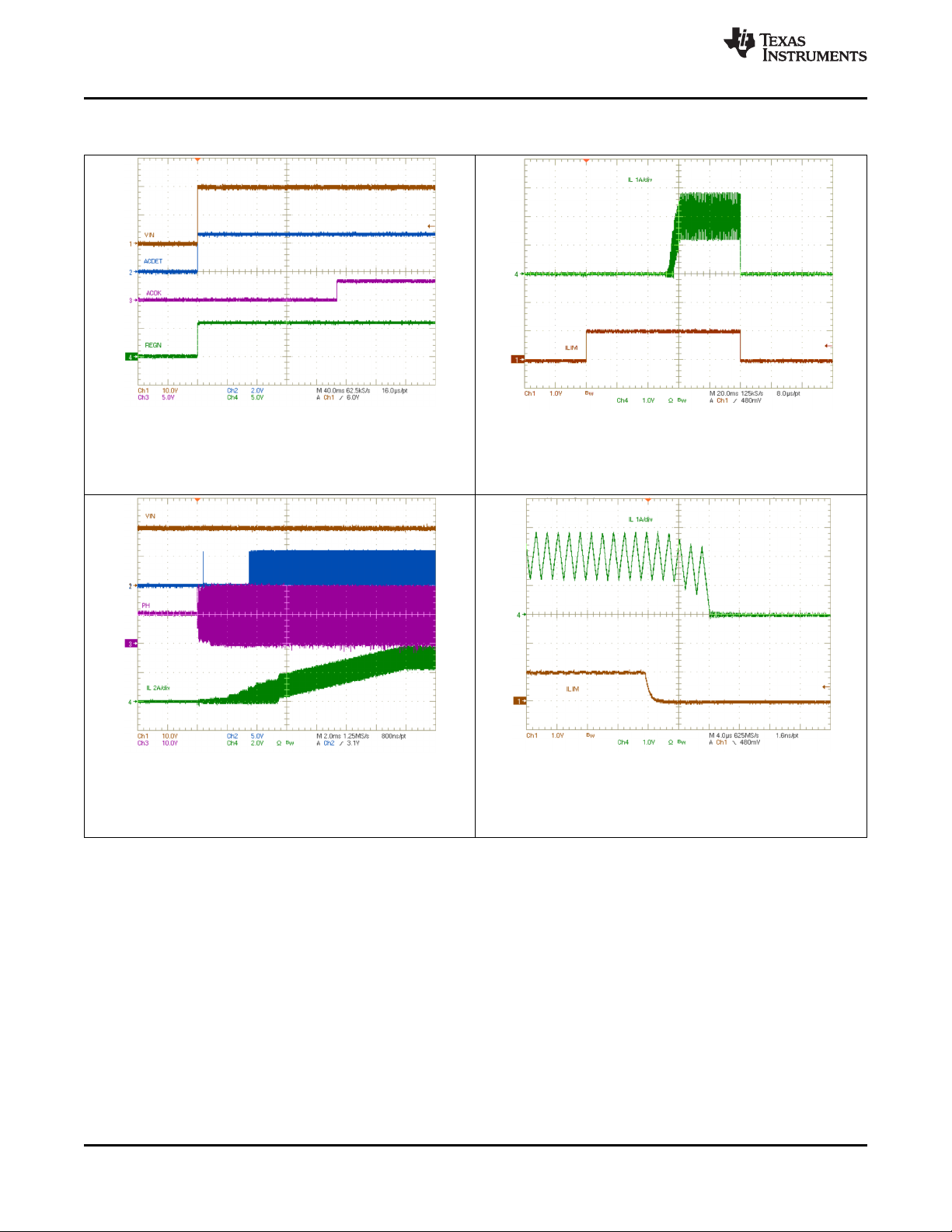
CH1: VCC, 10 V/div, CH2: ACDET, 2 V/div, CH3: ACOK, 5 V/div,
CH4: REGN, 5 V/div, 40 ms/div
Figure 1. VCC, ACDET, REGN and ACOK Power Up
CH1: Vin, 10 V/div, CH2: LODRV, 5 V/div,
CH3: PHASE, 10 V/div,
CH4: inductor current, 2 A/div, 2 ms/div
Figure 3. Current Soft-Start
CH1: ILIM, 1 V/div, CH4: inductor current, 1 A/div, 20 ms/div
Figure 2. Charge Enable by ILIM
CH1: ILIM, 1 V/div, CH4: inductor current, 1 A/div, 4 µs/div
Figure 4. Charge Disable by ILIM
10 Submit Documentation Feedback Copyright © 2011–2015, Texas Instruments Incorporated
Product Folder Links: bq24735
www.ti.com
Typical Characteristics (continued)
bq24735
SLUSAK9B –SEPTEMBER 2011–REVISED APRIL 2015
CH1: PHASE, 10 V/div, CH2: LODRV, 5 V/div,
CH3: HIDRV, 10 V/div
CH4: inductor current, 2 A/div, 400 ns/div
Figure 5. Continuous Conduction Mode Switching
Waveforms
CH1: PHASE, 10 V/div, CH2: LODRV, 5 V/div,
CH4: inductor current, 2 A/div, 4 µs/div
Figure 7. 100% Duty and Refresh Pulse
CH1: PHASE, 10 V/div, CH2: LODRV, 5 V/div,
CH3: HIDRV, 10 V/div,
CH4: inductor current, 1 A/div, 400 ns/div
Figure 6. Cycle-by-Cycle Synchronous to Nonsynchronous
CH2: battery current, 2 A/div, CH3: adapter current, 2 A/div,
CH4: system load current, 2 A/div, 100 µs/div
Figure 8. System Load Transient (Input DPM)
CH3: adapter current, 2 A/div, CH3: adapter current, 2 A/div,
CH4: battery current, 2 A/div, 10 ms/div CH4: battery current, 2 A/div, 10 ms/div
Figure 9. Buck-to-Boost Mode Figure 10. Boost-to-Buck Mode
Copyright © 2011–2015, Texas Instruments Incorporated Submit Documentation Feedback 11
Product Folder Links: bq24735
bq24735
SLUSAK9B –SEPTEMBER 2011–REVISED APRIL 2015
8 Parameter Measurement Information
www.ti.com
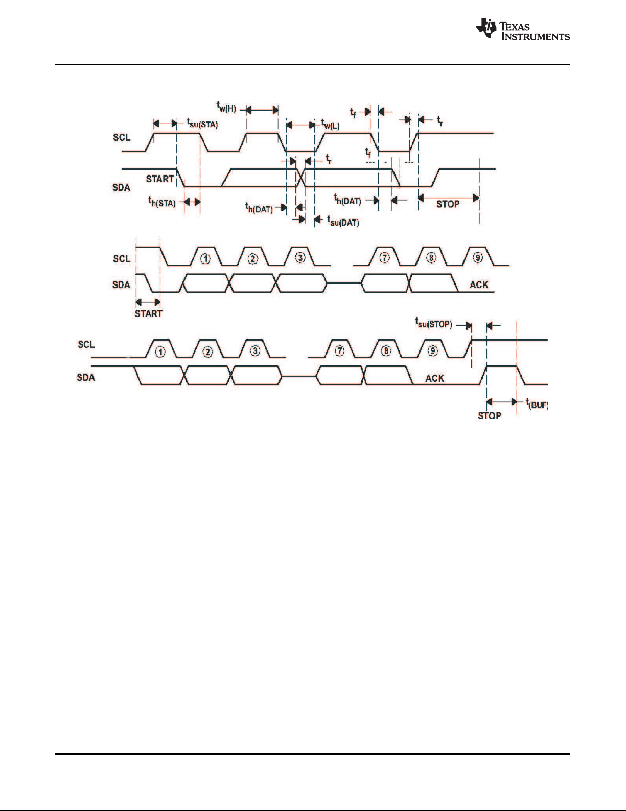
Figure 11. SMBus Communication Timing Waveforms
12 Submit Documentation Feedback Copyright © 2011–2015, Texas Instruments Incorporated
Product Folder Links: bq24735

bq24735
www.ti.com
SLUSAK9B –SEPTEMBER 2011–REVISED APRIL 2015
9 Detailed Description
9.1 Overview
The bq24735 device is a 1- to 4-cell battery charge controller with power selection for space-constrained,
multichemistry portable applications such as notebooks and detachable ultrabooks. The device supports wide
input range of input sources from 4.5 V to 24 V, and 1- to 4-cell battery for a versatile solution.
The bq24735 device supports automatic system power source selection with separate drivers for N-channel
MOSFETS on the adapter side and battery side.
The bq24735 device features Dynamic Power Management (DPM) to limit the input power and avoid AC adapter
overloading. During battery charging, as the system power increases, the charging current will reduce to maintain
total input current below adapter rating.
The SMBus controls input current, charge current and charge voltage registers with high-resolution, highaccuracy regulation limits.
Copyright © 2011–2015, Texas Instruments Incorporated Submit Documentation Feedback 13
Product Folder Links: bq24735
135
1.07
bq24735
SLUSAK9B –SEPTEMBER 2011–REVISED APRIL 2015
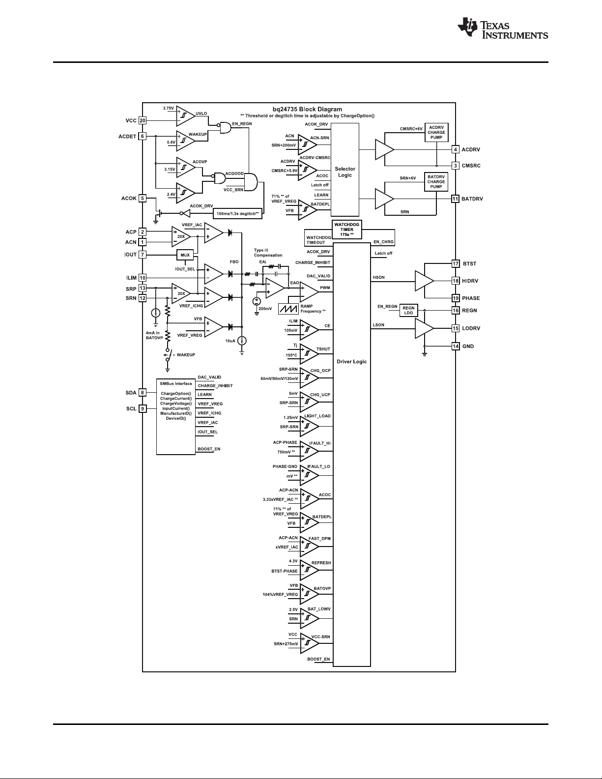
9.2 Functional Block Diagram
www.ti.com
14 Submit Documentation Feedback Copyright © 2011–2015, Texas Instruments Incorporated
Product Folder Links: bq24735

bq24735
www.ti.com
SLUSAK9B –SEPTEMBER 2011–REVISED APRIL 2015
9.3 Feature Description
9.3.1 Adapter Detect and ACOK Output
The bq24735 uses an ACOK comparator to determine the source of power on VCC pin, either from the battery or
adapter. An external resistor voltage divider attenuates the adapter voltage before it goes to ACDET. The
adapter detect threshold should typically be programmed to a value greater than the maximum battery voltage,
but lower than the maximum allowed adapter voltage.
The open-drain ACOK output requires external pullup resistor to system digital rail for a high level. It can be
pulled to external rail under the following conditions:
• V
• 2.4 V < V
• V
The first time after IC POR always gives 150-ms ACOK rising edge delay no matter what the ChargeOption
register value is. Only after the ACDET pin voltage is pulled below 2.4 V (but not below 0.6 V, which resets the
IC and forces the next ACOK rising edge deglitch time to be 1.3 s) and the ACFET has been turned off at least
one time, the 1.3 s (or 150 ms) delay time is effective for the next time the ACDET pin voltage goes above 2.4 V.
To change this option, the VCC pin voltage must above UVLO, and the ACDET pin voltage must be above 0.6 V
which enables the IC SMBus communication and sets ChargeOption() bit [15] to 0 which sets the next ACOK
rising deglitch time to be 150 ms. The purpose of the default 1.3 s rising edge deglitch time is to turn off the
ACFET long enough when the ACDET pin is pulled below 2.4 V by excessive system current, such as
overcurrent or short circuit.
VCC
VCC
> UVLO
ACDET
– V
SRN
< 3.15 V (not in ACOVP condition, nor in low input voltage condition)
> 275 mV (not in sleep mode)
9.3.2 Adapter Overvoltage (ACOVP)
When the ACDET pin voltage is higher than 3.15 V, it is considered as adapter overvoltage. ACOK will be pulled
low, and charge will be disabled. ACFET will be turned off to disconnect the high voltage adapter to system
during ACOVP. BATFET will be turned on if turnon conditions are valid. See System Power Selection for details.
When ACDET pin voltage falls below 3.15 V and above 2.4 V, it is considered as adapter voltage returns back to
normal voltage. ACOK will be pulled high by external pullup resistor. BATFET will be turned off and ACFET and
RBFET will be turned on to power the system from adapter. The charge can be resumed if enable charge
conditions are valid. See Enable and Disable Charging for details.
9.3.3 System Power Selection
The bq24735 automatically switches adapter or battery power to system. The battery is connected to system at
POR if battery exists. The battery is disconnected from system and the adapter is connected to system after
default 150 ms delay (first time, the next time default is 1.3 s and can be changed to 150 ms) if ACOK goes
HIGH. An automatic break-before-make logic prevents shoot-through currents when the selectors switch.
The ACDRV drives a pair of common-source (CMSRC) N-channel power MOSFETs (ACFET and RBFET)
between adapter and ACP (see Figure 16 for details). The ACFET separates adapter from battery or system, and
provides a limited DI/DT when plugging in adapter by controlling the ACFET turnon time. Meanwhile it protects
adapter when system or battery is shorted. The RBFET provides negative input voltage protection and battery
discharge protection when adapter is shorted to ground, and minimizes system power dissipation with its low
R
compared to a Schottky diode.
DS(on)
When the adapter is not present, ACDRV is pulled to CMSRC to keep ACFET and RBFET off, disconnecting
adapter from system. BATDRV stays at V
+ 6 V to connect battery to system if all the following conditions are
SRN
valid:
• V
• V
• V
> UVLO
VCC
> UVLO
SRN
< 200 mV above V
ACN
(ACN_SRN comparator)
SRN
Approximately 150 ms (first time; the next time default is 1.3 s and can be changed to 150 ms) after the adapter
is detected (ACDET pin voltage from 2.4 V to 3.15 V), the system power source begins to switch from battery to
adapter if all the following conditions are valid:
• Not in LEARN mode or in LEARN mode and V
is lower than battery depletion threshold
SRN
• ACOK high
Copyright © 2011–2015, Texas Instruments Incorporated Submit Documentation Feedback 15
Product Folder Links: bq24735

o
o o
1
=
2 L Cp
¦
bq24735
SLUSAK9B –SEPTEMBER 2011–REVISED APRIL 2015
Feature Description (continued)
www.ti.com
The gate drive voltage on ACFET and RBFET is V
+ 6 V. If the ACFET/RBFET have been turned on for 20
CMSRC
ms, and the voltage across gate and source is still less than 5.9 V, ACFET and RBFET will be turned off. After
1.3-s delay, it resumes turning on ACFET and RBFET. If such a failure is detected seven times within 90
seconds, ACFET/RBFET will be latched off and an adapter removal and system shut down is required to force
ACDET < 0.6 V to reset the IC. After IC reset from latch off, ACFET/RBFET can be turned on again. After 90
seconds, the failure counter will be reset to zero to prevent latch off. With ACFET/RBFET off, charge is disabled.
To turn off ACFET/RBFET, one of the following conditions must be valid:
• In LEARN mode and V
is above battery depletion threshold
SRN
• ACOK low
To limit the inrush current on ACDRV pin, CMSRC pin and BATDRV pin, a 4-kΩ resistor is recommended on
each of the three pins.
To limit the adapter inrush current when ACFET is turned on to power system from adapter, the Cgs and Cgd
external capacitor of ACFET must be carefully selected. The larger the Cgs and Cgd capacitance, the slower
turnon of ACFET will be and less inrush current of adapter. However, if Cgs or Cgd is too large, the ACDRVCMSRC voltage may still go low after the 20-ms turnon time window is expired. To make sure ACFET will not be
turned on when adapter is hot plugged in, the Cgs value should be 20 times or higher than Cgd. The most cost
effective way to reduce adapter inrush current is to minimize system total capacitance.
9.3.4 Automatic Internal Soft-Start Charger Current
Every time the charge is enabled, the charger automatically applies soft start on charge current to avoid any
overshoot or stress on the output capacitors or the power converter. The charge current starts at 128 mA, and
the step size is 64 mA in CCM mode for a 10-mΩ current sensing resistor. Each step lasts around 240 µs in
CCM mode until it reaches the programmed charge current limit. No external components are needed for this
function. During DCM mode, the soft start up current step size is larger and each step lasts for longer time period
due to the intrinsic slow response of DCM mode.
9.3.5 Converter Operation
The synchronous buck PWM converter uses a fixed-frequency voltage mode control scheme and internal type III
compensation network. The LC output filter gives a characteristic resonant frequency:
(1)
The resonant frequency (fo) is used to determine the compensation to ensure there is sufficient phase margin
and gain margin for the target bandwidth. The LC output filter should be selected to give a resonant frequency of
10–20 kHz nominal for the best performance. Suggested component value as charge current of 750-kHz default
switching frequency is shown in Table 1.
Ceramic capacitors show a DC-bias effect. This effect reduces the effective capacitance when a DC-bias voltage
is applied across a ceramic capacitor, as on the output capacitor of a charger. The effect may lead to a
significant capacitance drop, especially for high output voltages and small capacitor packages. See the
manufacturer's data sheet about the performance with a DC-bias voltage applied. It may be necessary to choose
a higher voltage rating or nominal capacitance value in order to get the required value at the operating point.
Table 1. Suggested Component Value as Charge Current of Default 750-kHz
Switching Frequency
Charge Current 2 A 3 A 4 A 6 A 8 A
Output Inductor Lo (µH) 6.8 or 8.2 5.6 or 6.8 3.3 or 4.7 3.3 2.2
Output Capacitor Co (µF) 20 20 20 30 40
Sense Resistor (mΩ) 10 10 10 10 10
16 Submit Documentation Feedback Copyright © 2011–2015, Texas Instruments Incorporated
Product Folder Links: bq24735

bq24735
www.ti.com
SLUSAK9B –SEPTEMBER 2011–REVISED APRIL 2015
The bq24735 has three loops of regulation: input current, charge current and charge voltage. The three loops are
brought together internally at the error amplifier. The maximum voltage of the three loops appears at the output
of the error amplifier EAO. An internal saw-tooth ramp is compared to the internal error control signal EAO (see
Functional Block Diagram) to vary the duty-cycle of the converter. The ramp has offset of 200 mV in order to
allow 0% duty-cycle.
When the battery charge voltage approaches the input voltage, EAO signal is allowed to exceed the saw-tooth
ramp peak in order to get a 100% duty-cycle. If voltage across BTST and PHASE pins falls below 4.3 V, a
refresh cycle starts and low-side N-channel power MOSFET is turned on to recharge the BTST capacitor. It can
achieve duty cycle of up to 99.5%.
9.3.6 Input Overcurrent Protection (ACOC)
The bq24735 cannot maintain the input current level if the charge current has been already reduced to zero.
After the system current continues increasing to the 3.33× of input current DAC set point (with 4.2-ms blank-out
time), ACFET/RBFET is latches off and an adapter removal and system shutdown is required to force ACDET <
0.6 V to reset IC. After IC reset from latch off, ACFET/RBFET can be turned on again.
The ACOC function threshold can be set to 3.33× of input DPM current or disable this function through SMBus
command (ChargeOption() bit [1]).
9.3.7 Charge Overcurrent Protection (CHGOCP)
The bq24735 has a cycle-by-cycle peak overcurrent protection. The device monitors the voltage across SRP and
SRN, and prevents the current from exceeding of the threshold based on the DAC charge current set point. The
high-side gate drive turns off for the rest of the cycle when the overcurrent is detected, and resumes when the
next cycle starts.
The charge OCP threshold is automatically set to 6 A, 9 A, and 12 A on a 10-mΩ current-sensing resistor based
on charge current register value. This prevents the threshold to be too high which is not safe or too low which
can be triggered in normal operation. Proper inductance should be selected to prevent OCP triggered in normal
operation due to high inductor current ripple.
9.3.8 Battery Overvoltage Protection (BATOVP)
The bq24735 will not allow the high-side and low-side MOSFET to turn on when the battery voltage at SRN
exceeds 104% of the regulation voltage set-point. If BATOVP last more than 30 ms, the charger is completely
disabled. This allows quick response to an overvoltage condition – such as occurs when the load is removed or
the battery is disconnected. A 4-mA current sink from SRP to GND is on only during BATOVP and allows
discharging the stored output inductor energy that is transferred to the output capacitors. Setting ChargeVoltage()
register value to 0 V will not trigger BATOVP function.
9.3.9 Battery Shorted to Ground (BATLOWV)
The bq24735 will limit inductor current if the battery voltage on SRN falls below 2.5 V after 1-ms charge is reset.
After 4-5 ms, the charge is resumed with soft start if all the enable conditions in Enable and Disable Charging are
satisfied. This prevents any overshoot current in inductor which can saturate inductor and may damage the
MOSFET. The charge current is limited to 0.5 A on 10-mΩ current-sensing resistor when BATLOWV condition
persists and LSFET remains off. The LSFET turns on only for a refreshing pulse to charge the BTST capacitor.
9.3.10 Thermal Shutdown Protection (TSHUT)
The QFN package has low thermal impedance, which provides good thermal conduction from the silicon to the
ambient, to keep junctions temperatures low. As added level of protection, the charger converter turns off for selfprotection whenever the junction temperature exceeds the 155°C. The charger stays off until the junction
temperature falls below 135°C. During thermal shutdown, the REGN LDO current limit is reduced to 16 mA.
Once the temperature falls below 135°C, charge can be resumed with soft start.
Copyright © 2011–2015, Texas Instruments Incorporated Submit Documentation Feedback 17
Product Folder Links: bq24735

bq24735
SLUSAK9B –SEPTEMBER 2011–REVISED APRIL 2015
www.ti.com
9.3.11 Inductor Short, MOSFET Short Protection
The bq24735 has a unique short-circuit protection feature. Its cycle-by-cycle current monitoring feature is
achieved through monitoring the voltage drop across R
of the MOSFETs after a certain amount of blanking
DS(on)
time. In case of MOSFET short or inductor short circuit, the overcurrent condition is sensed by two comparators
and two counters will be triggered. After seven times of short circuit events, the charger will be latched off and
ACFET and RBFET are turned off to disconnect adapter from system. BATFET is turned on to connect battery
pack to system. To reset the charger from latch-off status, the IC VCC pin must be pulled below UVLO or the
ACDET pin must be pulled below 0.6 V. This can be achieved by removing the adapter and shutting down the
operation system. The low-side MOSFET short circuit voltage drop threshold can be adjusted through SMBus
command. ChargeOption() bit [7] = 0, 1 sets the low-side threshold to 135 mV and 230 mV, respectively. The
high-side MOSFET short circuit voltage drop threshold can be adjusted through SMBus command.
ChargeOption() bit [8] = 0, 1 disables the function and sets the threshold to 750 mV, respectively. During boost
function, if the low-side MOSFET short-circuit protection threshold is used for cycle-by-cycle current limiting, the
charger will not latch up.
Due to the certain amount of blanking time to prevent noise when MOSFET just turns on, the cycle-by-cycle
charge overcurrent protection may detect high current and turn off MOSFET first before the short circuit
protection circuit can detect short condition because the blanking time has not finished. In such a case, the
charger may not be able to detect short circuit and counter may not be able to count to seven then latch off.
Instead, the charger may continuously keep switching with very narrow duty cycle to limit the cycle-by-cycle
current peak value. However, the charger should still be safe and will not cause failure because the duty cycle is
limited to a very short of time and MOSFET should be still inside the safety operation area. During a soft start
period, it may take a long time instead of just seven switching cycles to detect short circuit based on the same
blanking time reason.
9.4 Device Functional Modes
9.4.1 Enable and Disable Charging
In Charge mode, the following conditions have to be valid to start charge:
• Charge is enabled through SMBus (ChargeOption() bit [0] = 0, default is 0, charge enabled).
• ILIM pin voltage is higher than 105 mV.
• All three regulation limit DACs have valid value programmed.
• ACOK is valid (see Adapter Detect and ACOK Output for details).
• ACFET and RBFET turns on and gate voltage is high enough (see System Power Selection for details).
• V
• IC Temperature does not exceed TSHUT threshold.
• Not in ACOC condition (see Input Overcurrent Protection (ACOC) for details).
One of the following conditions will stop ongoing charging:
• Charge is inhibited through SMBus (ChargeOption() bit [0] = 1).
• ILIM pin voltage lower than 75 mV.
• One of three regulation limit DACs is set to 0 or out of range.
• ACOK is pulled low (see Adapter Detect and ACOK Output for details).
• ACFET turns off.
• V
• TSHUT IC temperature threshold is reached.
• ACOC is detected (see Input Overcurrent Protection (ACOC) for details).
• Short circuit is detected (see Inductor Short, MOSFET Short Protection for details).
• Watchdog timer expires if watchdog timer is enabled (see Charge Time-out for details).
does not exceed BATOVP threshold.
SRN
exceeds BATOVP threshold.
SRN
18 Submit Documentation Feedback Copyright © 2011–2015, Texas Instruments Incorporated
Product Folder Links: bq24735

bq24735
www.ti.com
SLUSAK9B –SEPTEMBER 2011–REVISED APRIL 2015
Device Functional Modes (continued)
9.4.2 Continuous Conduction Mode (CCM)
With sufficient charge current the bq24735’s inductor current never crosses zero, which is defined as continuous
conduction mode. The controller starts a new cycle with ramp coming up from 200 mV. As long as EAO voltage
is above the ramp voltage, the high-side MOSFET (HSFET) stays on. When the ramp voltage exceeds EAO
voltage, HSFET turns off and low-side MOSFET (LSFET) turns on. At the end of the cycle, ramp gets reset and
LSFET turns off, ready for the next cycle. There is always break-before-make logic during transition to prevent
cross-conduction and shoot-through. During the dead time when both MOSFETs are off, the body-diode of the
low-side power MOSFET conducts the inductor current.
During CCM mode, the inductor current is always flowing and creates a fixed two-pole system. Having the
LSFET turnon keeps the power dissipation low, and allows safely charging at high currents.
9.4.3 Discontinuous Conduction Mode (DCM)
During the HSFET off time when LSFET is on, the inductor current decreases. If the current goes to zero, the
converter enters Discontinuous Conduction Mode. Every cycle, when the voltage across SRP and SRN falls
below 5 mV (0.5 A on 10 mΩ), the undercurrent protection comparator (UCP) turns off LSFET to avoid negative
inductor current, which may boost the system via the body diode of HSFET.
During the DCM mode the loop response automatically changes. It changes to a single-pole system and the pole
is proportional to the load current.
Both CCM and DCM are synchronous operation with LSFET turnon every clock cycle. If the average charge
current goes below 125 mA on a 10-mΩ current sensing resistor, or the battery voltage falls below 2.5 V, the
LSFET keeps turnoff. The battery charger operates in nonsynchronous mode and the current flows through the
LSFET body diode. During nonsynchronous operation, the LSFET turns on only for a refreshing pulse to charge
the BTST capacitor. If the average charge current goes above 250 mA on a 10-mΩ current-sensing resistor, the
LSFET exits nonsynchronous mode and enters synchronous mode to reduce LSFET power loss.
9.5 Programming
9.5.1 SMBus Interface
The bq24735 device operates as a slave, receiving control inputs from the embedded controller host through the
SMBus interface. The bq24735 uses a simplified subset of the commands documented in System Management
Bus Specification V1.1, which can be downloaded from www.smbus.org. The bq24735 uses the SMBus ReadWord and Write-Word protocols (see Figure 12) to communicate with the smart battery. The bq24735 performs
only as a SMBus slave device with address 0b00010010 (0x12H) and does not initiate communication on the
bus. In addition, the bq24735 has two identification registers a 16-bit device ID register (0xFFH) and a 16-bit
manufacturer ID register (0xFEH).
SMBus communication is enabled with the following conditions:
• V
• V
The data (SDA) and clock (SCL) pins have Schmitt-trigger inputs that can accommodate slow edges. Choose
pullup resistors (10 kΩ) for SDA and SCL to achieve rise times according to the SMBus specifications.
Communication starts when the master signals a START condition, which is a high-to-low transition on SDA,
while SCL is high. When the master has finished communicating, the master issues a STOP condition, which is a
low-to-high transition on SDA, while SCL is high. The bus is then free for another transmission. Figure 13 and
Figure 14 show the timing diagram for signals on the SMBus interface. The address byte, command byte, and
data bytes are transmitted between the START and STOP conditions. The SDA state changes only while SCL is
low, except for the START and STOP conditions. Data is transmitted in 8-bit bytes and is sampled on the rising
edge of SCL. Nine clock cycles are required to transfer each byte in or out of the bq24735, because either the
master or the slave acknowledges the receipt of the correct byte during the ninth clock cycle. The bq24735
supports the charger commands as described in Table 2.
is above UVLO.
VCC
is above 0.6 V.
ACDET
Copyright © 2011–2015, Texas Instruments Incorporated Submit Documentation Feedback 19
Product Folder Links: bq24735

A =START CONDITION E=SLAVEPULLSSMBDATALINELOW I= ACKNOWLEDGECLOCKPULSE
B=MSBOF ADDRESSCLOCKEDINTOSLAVE F= ACKNOWLEDGEBIT CLOCKEDINTOMASTER J=STOP CONDITION
C=LSBOF ADDRESSCLOCKEDINTOSLAVE G=MSBOFDATACLOCKEDINTOMASTER K=NEWSTART CONDITION
D=R/WBIT CLOCKEDINTOSLAVE H=LSBOFDATA CLOCKEDINTOMASTER
A B C D EF G H IJK
t
LOWtHIGH
SMBCLK
SMBDATA
S
SLAVE
ADDRESS
W ACK
COMMAND
BYTE
ACK
LOW DATA
BYTE
ACK
HIGH DATA
BYTE
ACK P
7 BITS 1b 1b 8 BITS 1b 8 BITS 1b 8 BITS 1b
MSB LSB 0 0 MSB LSB 0 MSB LSB 0 MSB LSB 0
a) Write-Word Format
S
SLAVE
ADDRESS
W ACK
COMMAND
BYTE
ACK S
SLAVE
ADDRESS
R ACK
LOW DATA
BYTE
ACK
HIGH DATA
BYTE
NACK P
7 BITS 1b 1b 8 BITS 1b 7 BITS 1b 1b 8 BITS 1b 8 BITS 1b
MSB LSB 0 0 MSB LSB 0 MSB LSB 1 0 MSB LSB 0 MSB LSB 1
Preset to 0b0001001 DeviceID() = 0xFFH Preset to D7 D0 D15 D8
ManufactureID() = 0xFEH 0b0001001
ChargeCurrent() = 0x14H
ChargeVoltage() = 0x15H
InputCurrent() = 0x3FH
ChargeOption() = 0x12H LEGEND:
S = START CONDITION OR REPEATED START CONDITION P = STOP CONDITION
ACK = ACKNOWLEDGE (LOGIC-LOW) NACK = NOT ACKNOWLEDGE (LOGIC-HIGH)
W = WRITE BIT (LOGIC-LOW) R = READ BIT (LOGIC-HIGH)
b) Read-Word Format
MASTER TO SLAVE
SLAVE TO MASTER
Preset to 0b0001001
ChargeOption() = 0x12H
D7
D0 D15 D8
ChargeCurrent() = 0x14H
ChargeVoltage() = 0x15H
InputCurrent() = 0x3FH
bq24735
SLUSAK9B –SEPTEMBER 2011–REVISED APRIL 2015
Programming (continued)
www.ti.com
Figure 12. SMBus Write-Word and Read-Word Protocols
20 Submit Documentation Feedback Copyright © 2011–2015, Texas Instruments Incorporated
Figure 13. SMBus Write Timing
Figure 14. SMBus Read Timing
Product Folder Links: bq24735

bq24735
www.ti.com
SLUSAK9B –SEPTEMBER 2011–REVISED APRIL 2015
Programming (continued)
9.5.2 Battery LEARN Cycle
A battery LEARN cycle can be activated through SMBus command (ChargeOption() bit [6] = 1 enable LEARN
cycle, bit [6] = 0 disable LEARN cycle). When LEARN is enabled with ACFET/RBFET connected, the system
power selector logic is overdriven to switch to battery by turning off ACFET/RBFET and turning on BATFET.
LEARN function allows the battery to discharge in order to calibrate the battery gas gauge over a complete
discharge/charge cycle. The controller automatically exits LEARN cycle when the battery voltage is below battery
depletion threshold, and the system switches back to adapter input by turning off BATFET and turning on
ACFET/RBFET. After LEARN cycle, the LEARN bit is automatically reset to 0. The battery depletion threshold
can be set to 59.19%, 62.65%, 66.55%, and 70.97% of voltage regulation level through SMBus command
(ChargeOption() bit [12:11]).
9.5.3 Charge Time-out
The bq24735 includes a watchdog timer to terminate charging if the charger does not receive a write
ChargeVoltage() or write ChargeCurrent() command within 175 s (adjustable through ChargeOption() command).
If a watchdog time-out occurs all register values keep unchanged but charge is suspended. Write
ChargeVoltage() or write ChargeCurrent() commands must be resent to reset watchdog timer and resume
charging. The watchdog timer can be disabled, or set to 44 s, 88 s or 175 s through SMBus command
(ChargeOption() bit [14:13]). After watchdog time-out write ChargeOption() bit [14:13] to disable watchdog timer
also resume charging.
9.5.4 High-Accuracy Current-Sense Amplifier
As an industry standard, high-accuracy current-sense amplifier (CSA) is used to monitor the input current or the
charge current, selectable through SMBUS (ChargeOption() bit [5] = 0 select the input current, bit [5] = 1 select
the charge current) by host. The CSA senses voltage across the sense resistor by a factor of 20 through the
IOUT pin. Once VCC is above UVLO and ACDET is above 0.6 V, CSA turns on and IOUT output becomes valid.
To lower the voltage on current monitoring, a resistor divider from IOUT to GND can be used and accuracy over
temperature can still be achieved.
A 100-pF capacitor connected on the output is recommended for decoupling high-frequency noise. An additional
RC filter is optional, if additional filtering is desired.
NOTE
Adding filtering also increases response delay.
9.5.5 EMI Switching Frequency Adjust
The charger switching frequency can be adjusted ±18% to solve the EMI issue through SMBus command.
ChargeOption() bit [9] = 0 disables the frequency adjust function. To enable frequency adjust function, set
ChargeOption() bit [9] = 1. Set ChargeOption() bit [10] = 0 to reduce switching frequency, and set bit [10] = 1 to
increase switching frequency.
If frequency is reduced for a fixed inductor, the current ripple is increased. Inductor value must be carefully
selected so that it will not trigger cycle-by-cycle peak overcurrent protection, even for the worst conditions such
as higher input voltage, 50% duty cycle, lower inductance, and lower switching frequency.
Copyright © 2011–2015, Texas Instruments Incorporated Submit Documentation Feedback 21
Product Folder Links: bq24735

bq24735
SLUSAK9B –SEPTEMBER 2011–REVISED APRIL 2015
www.ti.com
9.6 Register Maps
9.6.1 Battery-Charger Commands
The bq24735 supports six battery-charger commands that use either Write-Word or Read-Word protocols, as
summarized in Table 2. ManufacturerID() and DeviceID() can be used to identify the bq24735. The
ManufacturerID() command always returns 0x0040H and the DeviceID() command always returns 0x001BH.
Table 2. Battery Charger Command Summary
REGISTER ADDRESS REGISTER NAME READ/WRITE DESCRIPTION POR STATE
0x12H ChargeOption() Read or Write Charger Options Control 0xF902H
0x14H ChargeCurrent() Read or Write 7-Bit Charge Current Setting 0x0000H
0x15H ChargeVoltage() Read or Write 11-Bit Charge Voltage Setting 0x0000H
0x3FH InputCurrent() Read or Write 6-Bit Input Current Setting 0x1000H
0XFEH ManufacturerID() Read Only Manufacturer ID 0x0040H
0xFFH DeviceID() Read Only Device ID 0x001BH
9.6.2 Setting Charger Options
By writing ChargeOption() command (0x12H or 0b00010010), bq24735 allows users to change several charger
options after POR (Power On Reset) as shown in Table 3.
9.6.3 Charge Options Register [reset = 0x12H] Figure 15. Charge Options Register
15 14 13 12 11 10 9 8
ACOK Deglitch WATCHDOG Timer Adjust BAT Depletion Comparator EMI Switching EMI Switching IFAULT_HI
Time Adjust Threshold Adjust Frequency Frequency Comparator
R/W R/W R/W R/W R/W R/W R/W
7 6 5 4 3 2 1 0
IFAULT_LOW LEARN Enable IOUT Selection AC Adapter BOOST Enable Boost Mode ACOC Charge Inhibit
Comparator Indication Indication Threshold
Threshold (Read Only) (Read Only) Adjust
Adjust
R/W R/W R/W R/W R/W R/W R/W R/W
LEGEND: R/W = Read/Write; R = Read only; -n = value after reset
Adjust Enable Threshold
Adjust
Table 3. Charge Options Field Descriptions
Bit Field Type Reset Description
[15] ACOK Deglitch Time Adjust R/W Adjust ACOK deglitch time.
After POR, the first time the adapter plug in occurs, deglitch time is
always 150 ms no matter if this bit is 0 or 1. This bit only sets the
next ACOK deglitch time after ACFET turns off at least one time. To
change this option, VCC pin voltage must be above UVLO and
ACDET pin voltage must be above 0.6 V to enable IC SMBus
communication.
0: ACOK rising edge deglitch time 150 ms
1: ACOK rising edge deglitch time 1.3 s <default at POR>
22 Submit Documentation Feedback Copyright © 2011–2015, Texas Instruments Incorporated
Product Folder Links: bq24735

www.ti.com
SLUSAK9B –SEPTEMBER 2011–REVISED APRIL 2015
Table 3. Charge Options Field Descriptions (continued)
Bit Field Type Reset Description
[14:13] WATCHDOG Timer Adjust R/W Set maximum delay between consecutive SMBus Write charge
[12:11] BAT Depletion Comparator R/W This is used for LEARN function and boost mode function battery
Threshold Adjust over discharge protection. During LEARN cycle, when the IC detects
[10] EMI Switching Frequency Adjust R/W 0: Reduce PWM switching frequency by 18% <default at POR>
[9] EMI Switching Frequency Enable R/W 0: Disable adjust PWM switching frequency <default at POR>
[8] IFAULT_HI Comparator Threshold R/W Short circuit protection high-side MOSFET voltage drop comparator
Adjust threshold.
[7] IFAULT_LOW Comparator R/W Short circuit protection low-side MOSFET voltage drop comparator
Threshold Adjust threshold. This is also used for cycle-by-cycle current limit protection
[6] LEARN Enable R/W Set this bit 1 start battery learn cycle. IC turns off ACFET and turns
[5] IOUT Selection R/W 0: IOUT is the 20x adapter current amplifier output <default at
[4] AC Adapter Indication (Read Only) R/W 0: AC adapter is not present (ACDET < 2.4 V) <default at POR>
[3] BOOST Enable R/W 0: Disable Turbo Boost function <default at POR>
[2] Boost Mode Indication (Read Only) R/W 0: Charger is not in boost mode <default at POR>
[1] ACOC Threshold Adjust R/W 0: function is disabled
voltage or charge current command. The charge will be suspended if
IC does not receive write charge voltage or write charge current
command within the watchdog time period and watchdog timer is
enabled.
The charge will be resumed after receive write charge voltage or
write charge current command when watchdog timer expires and
charge suspends. During boost function, the timer is fixed to 175 s if
it is enabled.
00: Disable Watchdog Timer
01: Enabled, 44 sec
10: Enabled, 88 sec
11: Enable Watchdog Timer (175 s) <default at POR>
battery voltage is below depletion voltage threshold, the IC turns off
BATFET and turned on ACFET to power the system from AC
adapter instead of the battery. During boost mode function, when the
IC detects battery voltage is below depletion voltage threshold, IC
stops boost function. The rising edge hysteresis is 340 mV. Set
ChargeVoltage() register value to 0 V will disable this function.
00: Falling Threshold = 59.19% of voltage regulation limit
(approximately 2.486 V/cell)
01: Falling Threshold = 62.65% of voltage regulation limit
(approximately 2.631 V/cell)
10: Falling Threshold = 66.55% of voltage regulation limit
(approximately 2.795 V/cell)
11: Falling Threshold = 70.97% of voltage regulation limit
(approximately 2.981 V/cell) < default at POR>
1: Increase PWM switching frequency by 18%
1: Enable adjust PWM switching frequency
0: function is disabled
1: 750 mV <default at POR>
threshold during boost function.
0: 135 mV <default at POR>
1: 230 mV
on BATFET to discharge battery capacity. When battery voltage
reaches threshold defined in bit [12;11], the BATFET is turned off
and ACFET is turned on to finish battery learn cycle. After finished
learn cycle, this bit is automatically reset to 0. Set this bit 0 will stop
battery learn cycle. IC turns off BATFET and turns on ACFET.
0: Disable LEARN Cycle <default at POR>
1: Enable LEARN Cycle
POR>
1: IOUT is the 20x charge current amplifier output
1: AC adapter is present (ACDET > 2.4 V)
1: Enable Turbo Boost function
1: Charger is in boost mode
1: 3.33x of input current regulation limit <default at POR>
bq24735
Copyright © 2011–2015, Texas Instruments Incorporated Submit Documentation Feedback 23
Product Folder Links: bq24735

( )
ILIM SRP SRN CHG SR
V = 20 × V V = 20 I R- ´ ´
bq24735
SLUSAK9B –SEPTEMBER 2011–REVISED APRIL 2015
www.ti.com
Table 3. Charge Options Field Descriptions (continued)
Bit Field Type Reset Description
[0] Charge Inhibit R/W 0: Enable Charge <default at POR>
1: Inhibit Charge
9.6.4 Setting the Charge Current
To set the charge current, write a 16-bit ChargeCurrent() command (0x14H or 0b00010100) using the data
format listed in Table 4. With 10-mΩ sense resistor, the bq24735 provides a charge current range of 128 mA to
8.128 A, with 64-mA step resolution. Sending ChargeCurrent() below 128 mA or above 8.128 A clears the
register and terminates charging. Upon POR, charge current is 0 A. TI recommends a 0.1-µF capacitor between
SRP and SRN for differential mode filtering, a 0.1-µF capacitor between SRN and ground for common mode
filtering, and an optional 0.1-µF capacitor between SRP and ground for common mode filtering. Meanwhile, the
capacitance on SRP should not be higher than 0.1 µF to properly sense the voltage across SRP and SRN for
cycle-by-cycle undercurrent and overcurrent detection.
The SRP and SRN pins are used to sense RSRwith default value of 10 mΩ. However, resistors of other values
can also be used. For a larger sense resistor, a larger sense voltage is given, and a higher regulation accuracy;
but, at the expense of higher conduction loss. If the current-sensing resistor value is too high, it may trigger an
overcurrent protection threshold because the current ripple voltage is too high. In such a case, either a higher
inductance value or a lower current-sensing resistor value should be used to limit the current ripple voltage level.
A current-sensing resistor value no more than 20 mΩ is suggested.
To provide secondary protection, the bq24735 has an ILIM pin with which the user can program the maximum
allowed charge current. Internal charge current limit is the lower one between the voltage set by
ChargeCurrent(), and voltage on ILIM pin. To disable this function, the user can pull ILIM above 1.6 V, which is
the maximum charge current regulation limit. Equation 2 shows the voltage set on the ILIM pin with respect to the
preferred charge current limit:
Table 4. Charge Current Register (0x14H), Using a 10-mΩ Sense Resistor
BIT BIT NAME DESCRIPTION
0 – Not used.
1 – Not used.
2 – Not used.
3 – Not used.
4 – Not used.
5 – Not used.
6 Charge Current, DACICHG 0 0 = Adds 0 mA of charger current.
1 = Adds 64 mA of charger current.
7 Charge Current, DACICHG 1 0 = Adds 0 mA of charger current.
1 = Adds 128 mA of charger current.
8 Charge Current, DACICHG 2 0 = Adds 0 mA of charger current.
1 = Adds 256 mA of charger current.
9 Charge Current, DACICHG 3 0 = Adds 0 mA of charger current.
1 = Adds 512 mA of charger current.
10 Charge Current, DACICHG 4 0 = Adds 0 mA of charger current.
1 = Adds 1024 mA of charger current.
11 Charge Current, DACICHG 5 0 = Adds 0 mA of charger current.
1 = Adds 2048 mA of charger current.
12 Charge Current, DACICHG 6 0 = Adds 0 mA of charger current.
1 = Adds 4096 mA of charger current.
13 – Not used.
14 – Not used.
15 – Not used.
(2)
24 Submit Documentation Feedback Copyright © 2011–2015, Texas Instruments Incorporated
Product Folder Links: bq24735

BATTERY BATTERY
INPUT LOAD BIAS
IN
I V
I = I + + I
V η
é ù
´
ê ú
´
ë û
bq24735
www.ti.com
SLUSAK9B –SEPTEMBER 2011–REVISED APRIL 2015
9.6.5 Setting the Charge Voltage
To set the output charge regulation voltage, write a 16-bit ChargeVoltage() command (0x15H or 0b0001#0101)
using the data format listed in Table 5. The bq24735 provides charge voltage range from 1.024 V to 19.200 V,
with a 16-mV step resolution. Sending ChargeVoltage() below 1.024 V or above 19.2 V clears the register and
terminates charging. Upon POR, charge voltage limit is 0 V.
The SRN pin is used to sense the battery voltage for voltage regulation and should be connected as close to the
battery as possible. Place a decoupling capacitor (0.1 µF recommended) as close to the IC as possible to
decouple high-frequency noise.
Table 5. Charge Voltage Register (0x15H)
BIT BIT NAME DESCRIPTION
0 - Not used.
1 - Not used.
2 - Not used.
3 - Not used.
4 Charge Voltage, DACV 0 0 = Adds 0 mV of charger voltage.
5 Charge Voltage, DACV 1 0 = Adds 0 mV of charger voltage.
6 Charge Voltage, DACV 2 0 = Adds 0 mV of charger voltage.
7 Charge Voltage, DACV 3 0 = Adds 0 mV of charger voltage.
8 Charge Voltage, DACV 4 0 = Adds 0 mV of charger voltage.
9 Charge Voltage, DACV 5 0 = Adds 0 mV of charger voltage.
10 Charge Voltage, DACV 6 0 = Adds 0 mV of charger voltage.
11 Charge Voltage, DACV 7 0 = Adds 0 mV of charger voltage.
12 Charge Voltage, DACV 8 0 = Adds 0 mV of charger voltage.
13 Charge Voltage, DACV 9 0 = Adds 0 mV of charger voltage.
14 Charge Voltage, DACV 10 0 = Adds 0 mV of charger voltage.
15 - Not used.
1 = Adds 16 mV of charger voltage.
1 = Adds 32 mV of charger voltage.
1 = Adds 64 mV of charger voltage.
1 = Adds 128 mV of charger voltage.
1 = Adds 256 mV of charger voltage.
1 = Adds 512 mV of charger voltage.
1 = Adds 1024 mV of charger voltage.
1 = Adds 2048 mV of charger voltage.
1 = Adds 4096 mV of charger voltage.
1 = Adds 8192 mV of charger voltage.
1 = Adds 16384 mV of charger voltage.
9.6.6 Setting Input Current
System current normally fluctuates as portions of the system are powered up or put to sleep. With the input
current limit, the output current requirement of the AC wall adapter can be lowered, reducing system cost.
The total input current, from a wall cube or other DC source, is the sum of the system supply current and the
current required by the charger. When the input current exceeds the set input current limit, the bq24735
decreases the charge current to provide priority to system load current. As the system current rises, the available
charge current drops linearly to zero. Thereafter, all input current goes to system load and input current
increases.
During DPM regulation, the total input current is the sum of the device supply current I
current, and the system load current I
where
• η is the efficiency of the charger buck converter (typically 85% to 95%). (3)
Copyright © 2011–2015, Texas Instruments Incorporated Submit Documentation Feedback 25
, and can be estimated as follows:
LOAD
Product Folder Links: bq24735
, the charger input
BIAS

bq24735
SLUSAK9B –SEPTEMBER 2011–REVISED APRIL 2015
www.ti.com
To set the input current limit, write a 16-bit InputCurrent() command (0x3FH or 0b0011#1111) using the data
format listed in Table 6. When using a 10-mΩ sense resistor, the bq24735 provides an input current-limit range
of 128 mA to 8.064 A, with 128-mA resolution. The suggested input current limit is set to no less than 512 mA.
Sending InputCurrent() below 128 mA or above 8.064 A clears the register and terminates charging. Upon POR,
the default input current limit is 4096 mA.
The ACP and ACN pins are used to sense RACwith default value of 10 mΩ. However, resistors of other values
can also be used. For a larger sense resistor, larger sense voltage is given, and a higher regulation accuracy;
but, at the expense of higher conduction loss.
If input current rises above FAST_DPM threshold, the charger will reduce charging current to allow the input
current drop. After a typical 260-µs delay time, if input current is still above FAST_DPM threshold, the charger
will shut down. When the system load current becomes smaller, the charger will soft restart to charge the battery
if the adapter still has power to charge the battery. This prevents a crash if the adapter is overloaded when the
system has a high and fast loading transient. The waiting time between shut down and restart charging is a
natural response time of the input current limit loop.
Table 6. Input Current Register (0x3FH), Using a 10-mΩ Sense Resistor
BIT BIT NAME DESCRIPTION
0 – Not used.
1 – Not used.
2 – Not used.
3 – Not used.
4 – Not used.
5 – Not used.
6 – Not used.
7 Input Current, DACIIN 0 0 = Adds 0 mA of input current.
1 = Adds 128 mA of input current.
8 Input Current, DACIIN 1 0 = Adds 0 mA of input current.
1 = Adds 256 mA of input current.
9 Input Current, DACIIN 2 0 = Adds 0 mA of input current.
1 = Adds 512 mA of input current.
10 Input Current, DACIIN 3 0 = Adds 0 mA of input current.
1 = Adds 1024 mA of input current.
11 Input Current, DACIIN 4 0 = Adds 0 mA of input current.
1 = Adds 2048 mA of input current.
12 Input Current, DACIIN 5 0 = Adds 0 mA of input current.
1 = Adds 4096 mA of input current.
13 – Not used.
14 – Not used.
15 – Not used.
9.6.7 Support Turbo Boost Function
The bq24735 supports Turbo Boost function when the adapter is above 16 V. During Turbo Boost mode, battery
discharge energy is delivered to system when system power demand is temporarily higher than adapter
maximum power level so that adapter will not crash. After POR, the ChargeOption() bit [3] is 0 which disable
Turbo Boost function. To enable it, the ChargeOption() bit [3] must be written to 1 by the host.
When input current is higher than the FAST_DPM comparator threshold, if Turbo Boost function is enabled,
charger IC will allow battery discharge and charger converter will change from buck converter to boost converter.
During Turbo Boost mode the adapter current is regulated at input current limit level so that adapter will not
crash. The battery discharge current depends on system current requirement and adapter current limit. The
SMBus timer can be enabled to prevent converter running at Turbo Boost mode for too long.
26 Submit Documentation Feedback Copyright © 2011–2015, Texas Instruments Incorporated
Product Folder Links: bq24735

VCC
BATDRV
REGN
BTST
HIDRV
PHASE
LODRV
GND
SRP
SRN
Q4
Sis412DN
L1
4.7µH
SYSTEM
C10
10µF
RSR
10mW
R1
430 kW
R2
66.5 kW
C2
0.1µF
U1
bq24735
C8
10uF
Q3
Sis412DN
Q5 (BATFET)
FDS6680A
C7
0.047µF
Adapter +
RAC 10mW
Pack +
C13
0.1µF
C6
1µF
HOST
Dig I/O
SMBus
+3.3V
C4
100 pF
R4
R5
R7
316 kW
ACN
ACP
CMSRC
ACDRV
ACDET
ILIM
SDA
SCL
ACOK
IOUT
Ci
2.2µF
Ri
2W
D2
BAT54C
R9
10 Ω
R3
10 kW
R8
100 kW
R10
4.02 kW
R11
EN
D1
BAT54
C14
0.1µF
C9
10uF
C11
10µF
Pack -
C3
0.1µF
C5
1µF
R6
C1
0.1µF
Total
Csys
220µF
C15
0.01µF
C16
0.1µF
C17
2200pF
Adapter -
ADC
U2
IMD2A
Q1 (ACFET)
FDS6680A
Q2 (RBFET)
FDS6680A
PowerPad
R12
1M
R13
3.01M
Q6
BSS138W
Reverse
Input
Protection
Dig I/O
EN
R14
10 Ω
R15
7.5 W
*
*
4.02 kW
10 kW
10 kW
4.02 kW
*
*
*
bq24735
www.ti.com
SLUSAK9B –SEPTEMBER 2011–REVISED APRIL 2015
10 Application and Implementation
NOTE
Information in the following applications sections is not part of the TI component
specification, and TI does not warrant its accuracy or completeness. TI’s customers are
responsible for determining suitability of components for their purposes. Customers should
validate and test their design implementation to confirm system functionality.
10.1 Application Information
The bq24725A/735EVM-710 evaluation module (EVM) is a complete charger module for evaluating the bq24735.
The application curves were taken using the bq24725A/735EVM-710. Refer to the EVM user's guide (SLUU507)
for EVM information.
10.2 Typical Application
ADPT
= 4.096 A, I
Figure 16. Typical System Schematic With Two NMOS Selectors
CHRG
= 2.944 A, I
Product Folder Links: bq24735
LIM
= 4 A, V
CHRG
= 12.592 V, 90-W adapter and 3S2P battery pack
Fs= 750 kHz, I
Use 0 Ω for better current-sensing accuracy, use 10-Ω or 7.5-Ω resistor for reversed battery connection protection.
See Negative Output Voltage Protection.
The total Csys is the lump sum of system capacitance. It is not required by charger IC. Use Ri and Ci for adapter hot
plug-in voltage spike damping. See Input Filter Design.
Copyright © 2011–2015, Texas Instruments Incorporated Submit Documentation Feedback 27

bq24735
SLUSAK9B –SEPTEMBER 2011–REVISED APRIL 2015
www.ti.com
Typical Application (continued)
10.2.1 Design Requirements
For this design example, use the parameters listed in Table 7 as the input parameters.
Table 7. Design Parameters
DESIGN PARAMETER EXAMPLE VALUE
Input Voltage
Input Current Limit
Battery Charge Voltage
Battery Charge Current
Battery Discharge Current
(1) Refer to adapter specification for settings for input voltage and input current limit.
(2) Refer to battery specification for settings.
10.2.2 Detailed Design Procedure
10.2.2.1 Negative Output Voltage Protection
If the battery pack is inserted in reverse order into the charger, output during production or hard shorts on
battery-to-ground generates negative output voltage on the SRP and SRN pins. IC internal electrostaticdischarge (ESD) diodes from the GND pin to the SRP or SRN pins and two anti-parallel (AP) diodes between the
SRP and SRN pins can be forward-biased and negative current can pass through the ESD diodes and AP
diodes when output has negative voltage. Insert two small resistors for SRP and SRN pins to limit the negative
current level when output has negative voltage. Suggested resistor value is 10 Ω for the SRP pin and 7 to 8 Ω for
the SRN pin. After adding small resistors, the suggested precharge current is at least 192 mA for a 10-mΩ
current-sensing resistor. Another method is using a small diode parallel with output capacitor; when battery
connection is reversed, the diode turns on and limits the negative voltage level. Using diode protection method
without insertion of small resistors into the SRP and SRN pins can get the best charging current accuracy.
(1)
(1)
(2)
(2)
(2)
17.7 V < Adapter Voltage < 24 V
3.2 A for 65-W adapter
12592 mV for 3-s battery
4096 mA for 3-s battery
6144 mA for 3-s battery
10.2.2.2 Reverse Input Voltage Protection
Q6, R12 and R13 in Figure 16 gives system and IC protection from reversed adapter voltage. In normal
operation, Q6 is turned off by negative Vgs. When adapter voltage is reversed, Q6 Vgs is positive. As a result,
Q6 turns on to short gate and source of Q2 so that Q2 is off. Q2 body diode blocks negative voltage to system.
However, CMSRC and ACDRV pins need R10 and R11 to limit the current due to the ESD diode of these pins
when turned on. Q6 must has low Vgs threshold voltage and low Qgs gate charge, so it turns on before Q2 turns
on. R10 and R11 must have enough power rating for the power dissipation when the ESD diode is on. In
Figure 21, the Schottky diode D3 gives the reverse adapter voltage protection, no extra small MOSFET and
resistors are needed.
In Figure 22, the Schottky diode Din is used for the reverse adapter voltage protection.
10.2.2.3 Reduce Battery Quiescent Current
When the adapter is not present, if VCC is powered with voltage higher than UVLO directly or indirectly (such as
through a LDO or switching converter) from battery, the internal BATFET charge pump gives the BATFET pin 6
V higher voltage than the SRN pin to drive the N-channel BATFET. As a result, the battery has higher quiescent
current. This is only necessary when the battery powers the system due to a high system current that goes
through the MOSFET channel instead of the body diode to reduce conduction loss and extend the battery
working life. When the system is totally shut down, it is not necessary to let the internal BATFET charge pump
work. The host controller can use a digital signal EN to disconnect the battery power path to the VCC pin by U2
in Figure 16. As a result, battery quiescent current can be minimized. The host controller still can get power from
BATFET body diode because the total system current is the lowest when the system is shut down, so there is no
high conduction loss of the body diode.
28 Submit Documentation Feedback Copyright © 2011–2015, Texas Instruments Incorporated
Product Folder Links: bq24735

RIPPLE
COUT RIPPLE
I
I = 0.29 I
2 3
» ´
´
CIN CHG
I = I D × (1 D)´ -
IN
RIPPLE
S
V D (1 D)
I =
Lf
´ ´ -
´
SAT CHG RIPPLE
I I + (1/2) I³
bq24735
www.ti.com
SLUSAK9B –SEPTEMBER 2011–REVISED APRIL 2015
10.2.2.4 Inductor Selection
The bq24735 has three selectable fixed switching frequencies. Higher switching frequency allows the use of
smaller inductor and capacitor values. Inductor saturation current should be higher than the charging current
(I
) plus half the ripple current (I
CHG
The inductor ripple current depends on input voltage (VIN), duty cycle (D = V
RIPPLE
):
(4)
OUT/VIN
), switching frequency (fS) and
inductance (L):
(5)
The maximum inductor ripple current happens with D = 0.5 or close to 0.5. For example, the battery charging
voltage range is from 9 V to 12.6 V for a 3-cell battery pack. For 20-V adapter voltage, a 10-V battery voltage
gives the maximum inductor ripple current. Another example is a 4-cell battery. The battery voltage range is from
12 V to 16.8 V, and 12-V battery voltage gives the maximum inductor ripple current.
Usually, inductor ripple is designed in the range of (20% to 40%) maximum charging current as a trade-off
between inductor size and efficiency for a practical design.
The bq24735 has charge undercurrent protection (UCP) by monitoring charging current-sensing resistor cycleby-cycle. The typical cycle-by-cycle UCP threshold is 5-mV falling edge corresponding to 0.5-A falling edge for a
10-mΩ charging current sensing resistor. When the average charging current is less than 125 mA for a 10-mΩ
charging current-sensing resistor, the low-side MOSFET is off until BTST capacitor voltage must refresh the
charge. As a result, the converter relies on low-side MOSFET body diode for the inductor freewheeling current.
10.2.2.5 Input Capacitor
Input capacitor should have enough ripple current rating to absorb input switching ripple current. The worst-case
RMS ripple current is half of the charging current when duty cycle is 0.5. If the converter does not operate at
50% duty cycle, then the worst-case capacitor RMS current occurs where the duty cycle is closest to 50% and
can be estimated by Equation 6:
(6)
Low ESR ceramic capacitor such as X7R or X5R is preferred for input decoupling capacitor and should be
placed to the drain of the high-side MOSFET and source of the low-side MOSFET as close as possible. Voltage
rating of the capacitor must be higher than normal input voltage level. 25-V rating or higher capacitor is preferred
for 19- to 20-V input voltage. 10- to 20-μF capacitance is suggested for typical of 3- to 4-A charging current.
Ceramic capacitors show a DC-bias effect. This effect reduces the effective capacitance when a DC-bias voltage
is applied across a ceramic capacitor, as on the input capacitor of a charger. The effect may lead to a significant
capacitance drop, especially for high input voltages and small capacitor packages. See the manufacturer's data
sheet about the performance with a DC-bias voltage applied. It may be necessary to choose a higher voltage
rating or nominal capacitance value in order to get the required value at the operating point.
10.2.2.6 Output Capacitor
Output capacitor also should have enough ripple current rating to absorb output switching ripple current. The
output capacitor RMS current is given:
(7)
The bq24735 has internal loop compensator. To get good loop stability, the resonant frequency of the output
inductor and output capacitor should be designed between 10 kHz and 20 kHz. The preferred ceramic capacitor
is a 25-V X7R or X5R for output capacitor. A capacitance of 10 to 20 µF is suggested for a typical of 3- to 4-A
charging current. Place the capacitors after charging current-sensing resistor to get the best charge current
regulation accuracy.
Copyright © 2011–2015, Texas Instruments Incorporated Submit Documentation Feedback 29
Product Folder Links: bq24735

REGN plt plt
on off
on off
V - V V
I = , I =
R R
SW GD GS
1
Q = Q + Q2´
SW SW
on off
on off
Q Q
t = , t =
I I
2
top CHG DS(on) IN CHG on off s
1
P = D I R + V I (t + t )2f´ ´ ´ ´ ´ ´
bq24735
SLUSAK9B –SEPTEMBER 2011–REVISED APRIL 2015
www.ti.com
Ceramic capacitors show a DC-bias effect. This effect reduces the effective capacitance when a DC-bias voltage
is applied across a ceramic capacitor, as on the output capacitor of a charger. The effect may lead to a
significant capacitance drop, especially for high output voltages and small capacitor packages. See the
manufacturer's data sheet about the performance with a DC-bias voltage applied. It may be necessary to choose
a higher voltage rating or nominal capacitance value in order to get the required value at the operating point.
10.2.2.7 Power MOSFETs Selection
Two external N-channel MOSFETs are used for a synchronous switching battery charger. The gate drivers are
internally integrated into the IC with 6 V of gate drive voltage. A 30-V or higher voltage rating MOSFETs are
preferred for 19- to 20-V input voltage.
Figure-of-merit (FOM) is usually used for selecting proper MOSFET based on a tradeoff between the conduction
loss and switching loss. For the top-side MOSFET, FOM is defined as the product of a MOSFET ON-resistance,
R
MOSFET ON-resistance, R
The lower the FOM value, the lower the total power loss. Usually lower R
, and the gate-to-drain charge, QGD. For the bottom-side MOSFET, FOM is defined as the product of the
DS(ON)
FOM
top
= R
DS(on)
x QGD; FOM
, and the total gate charge, QG.
DS(ON)
bottom
= R
DS(on)
x Q
G
has higher cost with the same
DS(ON)
(8)
package size.
The top-side MOSFET loss includes conduction loss and switching loss. It is a function of duty cycle
(D=V
OUT/VIN
(fS), turnon time (ton) and turnoff time (t
), charging current (I
), MOSFET ON-resistance (R
CHG
):
off
), input voltage (VIN), switching frequency
DS(ON)
(9)
The first item represents the conduction loss. Usually MOSFET R
increases by 50% with 100°C junction
DS(ON)
temperature rise. The second term represents the switching loss. The MOSFET turnon and turnoff times are
given by:
(10)
where Qswis the switching charge, Ionis the turnon gate driving current and I
is the turnoff gate driving current.
off
If the switching charge is not given in MOSFET data sheet, it can be estimated by gate-to-drain charge (QGD)
and gate-to-source charge (QGS):
(11)
Gate driving current can be estimated by REGN voltage (V
gate resistance (Ron) and turnoff gate resistance (R
) of the gate driver:
off
), MOSFET plateau voltage (V
REGN
), total turnon
plt
(12)
The conduction loss of the bottom-side MOSFET is calculated with the following equation when it operates in
synchronous continuous conduction mode:
P
bottom
= (1 - D) x I
CHG
2
x R
DS(on)
(13)
When charger operates in nonsynchronous mode, the bottom-side MOSFET is off. As a result all the
freewheeling current goes through the body-diode of the bottom-side MOSFET. The body diode power loss
depends on its forward voltage drop (VF), nonsynchronous mode charging current (I
PD= VFx I
NONSYNC
x (1 - D) (14)
NONSYNC
), and duty cycle (D).
The maximum charging current in nonsynchronous mode can be up to 0.25 A for a 10-mΩ charging current
sensing resistor, or 0.5 A if battery voltage is below 2.5 V. The minimum duty cycle happens at lowest battery
voltage. Choose the bottom-side MOSFET with either an internal Schottky or body diode capable of carrying the
maximum nonsynchronous mode charging current.
30 Submit Documentation Feedback Copyright © 2011–2015, Texas Instruments Incorporated
Product Folder Links: bq24735

PHASE
Battery
Adapter
ACP
ACN
R
AC
BTST
REGN
High-Side
MOSFET
Low-Side
MOSFET
CLR
Count to 7
Adapter
Plug in
R
DC
L
Latch off
Charger
SCP1
SCP2
COMP1
COMP2
R
PCB
C
R1(2010)
2Ω
C1
2.2μF
D1
C2
0.47-1μF
R2(1206)
10-20 Ω
Adapter
connector
VCC pin
bq24735
www.ti.com
SLUSAK9B –SEPTEMBER 2011–REVISED APRIL 2015
10.2.2.8 Input Filter Design
During adapter hot plug-in, the parasitic inductance and input capacitor from the adapter cable form a second
order system. The voltage spike at VCC pin maybe beyond IC maximum voltage rating and damage IC. The
input filter must be carefully designed and tested to prevent overvoltage event on VCC pin.
There are several methods of damping or limiting the overvoltage spike during adapter hot plug-in. An electrolytic
capacitor with high ESR as an input capacitor can damp the overvoltage spike well below the IC maximum pin
voltage rating. A high current capability TVS Zener diode can also limit the overvoltage level to an IC safe level.
However, these two solutions may not have low cost or small size.
A cost-effective and small-size solution is shown in Figure 17. R1 and C1 are composed of a damping RC
network to damp the hot plug-in oscillation. As a result the overvoltage spike is limited to a safe level. D1 is used
for reverse voltage protection for VCC pin. C2 is VCC pin decoupling capacitor and it should be place to VCC pin
as close as possible. C2 value should be less than C1 value so R1 can dominant the equivalent ESR value to
get enough damping effect. R2 is used to limit inrush current of D1 to prevent D1 getting damage when adapter
hot plug-in. R2 and C2 should have 10-us time constant to limit the DV/DT on VCC pin to reduce inrush current
when adapter hot plug in. R1 has high inrush current. R1 package must be sized enough to handle inrush current
power loss according to resistor manufacturer’s data sheet. The filter components value always must be verified
with real application and minor adjustments may need to fit in the real application circuit.
Figure 17. Input Filter
10.2.2.9 bq24735 Design Guideline
The bq24735 has a unique short-circuit protection feature. Its cycle-by-cycle current monitoring feature is
achieved through monitoring the voltage drop across R
of the MOSFETs after a certain amount of blanking
DS(on)
time. For a MOSFET short or inductor short circuit, the overcurrent condition is sensed by two comparators, and
two counters are triggered. After seven occurrences of a short-circuit event, the charger will be latched off. To
reset the charger from latch-off status, reconnect the adapter. Figure 18 shows the bq24735 short-circuit
protection block diagram.
Copyright © 2011–2015, Texas Instruments Incorporated Submit Documentation Feedback 31
Figure 18. Block Diagram of bq24735 Short-Circuit Protection
Product Folder Links: bq24735

bq24735
SLUSAK9B –SEPTEMBER 2011–REVISED APRIL 2015
www.ti.com
In normal operation, the low-side MOSFET current is from source to drain which generates a negative voltage
drop when it turns on. As a result, the overcurrent comparator cannot be triggered. When the high-side switch
short circuit or inductor short circuit occurs, the large current of the low-side MOSFET is from drain to source and
can trigger the low-side switch overcurrent comparator. bq24735 senses the low-side switch voltage drop through
the PHASE pin and the GND pin.
The high-side FET short is detected by monitoring the voltage drop between ACP and PHASE. As a result, it not
only monitors the high-side switch voltage drop, but also the adapter-sensing resistor voltage drop and PCB
trace voltage drop from the ACN terminal of RACto the charger high-side switch drain. Usually, there is a long
trance between input-sensing resistor and charger-converting input, a careful layout will minimize the trace effect.
Table 8. Component List for Typical System Circuit of Figure 16
PART DESIGNATOR QTY DESCRIPTION
C1, C2, C3, C13, C14, C16 6 Capacitor, Ceramic, 0.1 µF, 25 V, 10%, X7R, 0603
C4 1 Capacitor, Ceramic, 100 pF, 25 V, 10%, X7R, 0603
C5, C6 2 Capacitor, Ceramic, 1 µF, 25 V, 10%, X7R, 0603
C7 1 Capacitor, Ceramic, 0.047 µF, 25 V, 10%, X7R, 0603
C8, C9, C10, C11 4 Capacitor, Ceramic, 10 µF, 25 V, 10%, X7R, 1206
C15 1 Capacitor, Ceramic, 0.01 µF, 25 V, 10%, X7R, 0603
C17 1 Capacitor, Ceramic, 2200 pF, 25 V, 10%, X7R, 0603
Ci 1 Capacitor, Ceramic, 2.2 µF, 25 V, 10%, X7R, 1210
Csys 1 Capacitor, Electrolytic, 220 µF, 25 V
D1 1 Diode, Schottky, 30 V, 200 mA, SOT-23, Fairchild, BAT54
D2 1 Diode, Dual Schottky, 30 V, 200 mA, SOT-23, Fairchild, BAT54C
Q1, Q2, Q5 3 N-channel MOSFET, 30 V, 12.5 A, SO-8, Fairchild, FDS6680A
Q3, Q4 2 N-channel MOSFET, 30 V, 12 A, PowerPAK 1212-8, Vishay Siliconix, SiS412DN
Q6 1 N-channel MOSFET, 50 V, 0.2 A, SOT-323, Diodes, BSS138W
L1 1 Inductor, SMT, 4.7 µH, 5.5 A, Vishay Dale, IHLP2525CZER4R7M01
R1 1 Resistor, Chip, 430 kΩ, 1/10 W, 1%, 0603
R2 1 Resistor, Chip, 66.5 kΩ, 1/10 W, 1%, 0603
R3, R4, R5 3 Resistor, Chip, 10 kΩ, 1/10 W, 1%, 0603
R6, R10, R11 3 Resistor, Chip, 4.02 kΩ, 1/10 W, 1%, 0603
R7 1 Resistor, Chip, 316 kΩ, 1/10 W, 1%, 0603
R8 1 Resistor, Chip, 100 kΩ, 1/10 W, 1%, 0603
R9 1 Resistor, Chip, 10 Ω, 1/4 W, 1%, 1206
R12 1 Resistor, Chip, 1.00 MΩ, 1/10 W, 1%, 0603
R13 1 Resistor, Chip, 3.01 MΩ, 1/10 W, 1%, 0603
R14 1 Resistor, Chip, 10 Ω, 1/10 W, 5%, 0603
R15 1 Resistor, Chip, 7.5 Ω, 1/10 W, 5%, 0603
RAC, RSR 2 Resistor, Chip, 0.01 Ω, 1/2 W, 1%, 1206
Ri 1 Resistor, Chip, 2 Ω, 1/2 W, 1%, 1210
U1 1 Charger controller, 20-pin VQFN, TI, bq24735RGR
U2 1 Dual digital transistor, 40 V, 30 mA, SC-74, Rohm, IMD2A
32 Submit Documentation Feedback Copyright © 2011–2015, Texas Instruments Incorporated
Product Folder Links: bq24735

VCC
BATDRV
REGN
BTST
HIDRV
PHASE
LODRV
GND
SRP
SRN
Q4
Sis412DN
L1
4.7µH
SYSTEM
C10
10µF
RSR
10mW
R1
430 kW
R2
66.5 kW
C2
0.1µF
U1
bq24735
C8
10uF
Q3
Sis412DN
Q5 (BATFET)
FDS6680A
C7
0.047µF
Adapter +
RAC 10 mW
Pack +
C6
1µF
HOST
Dig I/O
SMBus
+3.3V
C4
100 pF
R4
R5
R7
549 kW
ACN
ACP
CMSRC
ACDRV
ACDET
ILIM
SDA
SCL
ACOK
IOUT
Ci
2.2µF
Ri
2 W
R9
10 Ω
R3
10 kW
R8
100 kW
R10
4.02 kW
R11
D1
BAT54
C9
10uF
C11
10µF
Pack -
C3
0.1µF
C5
1µF
R6
4.02 kW
C1
0.1µF
Total
Csys
220µF
C15
0.01µF
C16
0.1µF
C17
2200 pF
Adapter -
ADC
Q1 (ACFET)
FDS6680A
D3
PDS1040
PowerPad
C13
0.1µF
C14
0.1µF
R14
10 Ω
R15
7.5 Ω
*
*
4.02 kW
10 kW
10 kW
*
*
*
88
89
90
91
92
93
94
95
96
97
98
0 0.5 1 1.5 2 2.5 3 3.5 4 4.5
Charge Current
4-cell 16.8 V
3-cell 12.6 V
2-cell 8.4 V
Efficiency (%)
www.ti.com
10.2.3 Application Curves
bq24735
SLUSAK9B –SEPTEMBER 2011–REVISED APRIL 2015
CH1: PHASE, 20 V/div, CH2: battery voltage, 5 V/div,
10.3 System Examples
Copyright © 2011–2015, Texas Instruments Incorporated Submit Documentation Feedback 33
Fs= 750 kHz, I
pack
Use 0 Ω for better current-sensing accuracy, use 10-Ω or 7.5-Ω resistor for reversed battery connection protection.
See Negative Output Voltage Protection.
The total Csys is the lump sum of system capacitance. It is not required by charger IC. Use Ri and Ci for adapter hot
plug-in voltage spike damping. See Input Filter Design.
Figure 21. Typical System Schematic With One NMOS Selector and Schottky Diode
CH3: LODRV, 10 V/div,
CH4: inductor current, 2 A/div, 400 µs/div
Figure 19. Battery Insertion
ADPT
= 2.816 A, I
CHRG
= 1.984 A, I
Product Folder Links: bq24735
LIM
= 2.54 A, V
VIN= 20 V FS= 750 kHz L = 4.7 µH
Figure 20. Efficiency vs Output Current
= 12.592 V, 65-W adapter and 3S2P battery
CHRG

VCC
BATDRV
REGN
BTST
HIDRV
PHASE
LODRV
GND
SRP
SRN
Q4
Sis412DN
L1
4.7µH
SYSTEM
C10
10
µF
RSR
10 mW
R1
430 kW
R2
487 kW
C2
0.1µF
U1
bq247 35
C8
10uF
Q3
Sis412DN
C7
0.047µF
Adapter +
RAC 10 mW
Pack +
C6
1µF
HOST
Dig I/O
SMBus
+3.3V
C4
100 pF
R4
R5
R7
549
kW
ACN
ACP
CMSRC
ACDRV
ACDET
ILIM
SDA
SCL
ACOK
IOUT
Din
BAT54A
R9
4.7 W
R3
10 kW
R8
100 kW
R10
4.02 kW
R11
4.02 kW
D1
BAT54
C9
10uF
C11
10 µF
Pack -
C3
0.1µF
C5
1µF
R6
4.02 kW
C1
0.1 µF
Total
Csys
220
µF
Adapter -
ADC
Q1 (ACFET)
FDS6680A
Q2 (RBFET)
FDS6680A
PowerPad
C13
0.1µF
C14
0.1µF
R14
10 W
R15
7.5 W
*
*
C17
2200pF
C16
0.047µF
R12
100 kW
Q5 (BATFET)
Si4435DDY
D2
SL42
10 kW
10 kW
*
*
bq24735
SLUSAK9B –SEPTEMBER 2011–REVISED APRIL 2015
System Examples (continued)
www.ti.com
Fs= 750 kHz, I
ADPT
= 2.048 A, I
CHRG
= 1.984 A, I
= 2.54 A, V
LIM
= 4.200 V, 12-W adapter and 1S2P battery
CHRG
pack
Use 0 Ω for better current-sensing accuracy, use 10-Ω or 7.5-Ω resistor for reversed battery connection protection.
See Negative Output Voltage Protection.
The total Csys is the total lump sum of system capacitance. It is not required by charger IC. Use Din for reverse input
voltage protection. See Input Filter Design.
Figure 22. Typical System Schematic for 5-V Input 1-S Battery
34 Submit Documentation Feedback Copyright © 2011–2015, Texas Instruments Incorporated
Product Folder Links: bq24735

bq24735
www.ti.com
SLUSAK9B –SEPTEMBER 2011–REVISED APRIL 2015
11 Power Supply Recommendations
When adapter is attached, and ACOK goes HIGH, the system is connected to adapter through ACFET/RBFET.
An external resistor voltage divider attenuates the adapter voltage before it goes to ACDET. The adapter detect
threshold should typically be programmed to a value greater than the maximum battery voltage, but lower than
the IC maximum allowed input voltage and system maximum allowed voltage.
When adapter is removed, the system is connected to battery through BATFET. Typically the battery depletion
threshold should be greater than the minimum system voltage so that the battery capacity can be fully used for
maximum battery life.
12 Layout
12.1 Layout Guidelines
The switching node rise and fall times should be minimized for minimum switching loss. Proper layout of the
components to minimize high-frequency current path loop (see Figure 25) is important to prevent electrical and
magnetic field radiation and high-frequency resonant problems. The following procedure shows a PCB layout
priority list for proper layout. Layout PCB according to this specific order is essential.
1. Place the input capacitor as close as possible to the supply and ground connections of the switching
MOSFET and use shortest copper trace connection. These parts should be placed on the same layer of PCB
instead of on different layers and using vias to make this connection.
2. The IC should be placed close to the gate terminals of the switching MOSFET and keep the gate drive signal
traces short for a clean MOSFET drive. The IC can be placed on the other side of the PCB of switching
MOSFETs.
3. Place the inductor input terminal as close as possible to the output terminal of the switching MOSFET.
Minimize the copper area of this trace to lower electrical and magnetic field radiation but make the trace wide
enough to carry the charging current. Do not use multiple layers in parallel for this connection. Minimize
parasitic capacitance from this area to any other trace or plane.
4. Place the charging current-sensing resistor right next to the inductor output. Route the sense leads
connected across the sensing resistor back to the IC in same layer, close to each other (minimize loop area)
and do not route the sense leads through a high-current path (see Figure 26 for Kelvin connection for best
current accuracy). Place the decoupling capacitor on these traces next to the IC.
5. Place the output capacitor next to the sensing resistor output and ground
6. Output capacitor ground connections must be tied to the same copper that connects to the input capacitor
ground before connecting to system ground.
7. Use a single ground connection to tie charger power ground to charger analog ground. Use analog ground
copper pour just beneath the IC, but avoid power pins to reduce inductive and capacitive noise coupling.
8. Route analog ground separately from power ground. Connect analog ground and connect power ground
separately. Connect analog ground and power ground together, using power pad as the single ground
connection point, or using a 0-Ω resistor to tie analog ground to power ground (power pad should tie to
analog ground in this case if possible).
9. Place the decoupling capacitors next to the IC pins and make trace connection as short as possible.
10. It is critical that the exposed power pad on the backside of the IC package be soldered to the PCB ground.
Ensure that there are sufficient thermal vias directly under the IC, connecting to the ground plane on the
other layers.
11. The via size and number should be enough for a given current path.
See the EVM design for the recommended component placement with trace and via locations. For the QFN
information, see SCBA017 and SLUA271.
Copyright © 2011–2015, Texas Instruments Incorporated Submit Documentation Feedback 35
Product Folder Links: bq24735

ToACP To ACN
Systemcurrent
Chargerinputcurrent
SinglepointconnectionatR
AC
SystemPathPCB Trace
ChargerInputPCB Trace
R
AC
ACP ACN
Charger
R
AC
R
PCB
I
CHRGIN
I
BAT
I
SYS
I
DPM
(a)PCBLayout (b)EquivalentCircuit
R
AC
ToACP
ToACN
SystemPathPCB Trace
Systemcurrent
Chargerinputcurrent
ChargerInputPCB Trace
ACP ACN
R
AC
Charger
R
PCB
I
CHRGIN
I
BAT
I
SYS
I
DPM
(a)PCBLayout (b)EquivalentCircuit
bq24735
SLUSAK9B –SEPTEMBER 2011–REVISED APRIL 2015
Layout Guidelines (continued)
www.ti.com
To prevent unintentional charger shut down in normal operation, MOSFET R
selection and PCB layout is
DS(on)
very important. Figure 23 shows a improvement PCB layout example and its equivalent circuit. In this layout, the
system current path and charger input current path is not separated, as a result, the system current causes
voltage drop in the PCB copper and is sensed by the IC. The worst layout is when a system current pull point is
after charger input; as a result all system current voltage drops are counted into overcurrent protection
comparator. The worst case for IC is when the total system current and charger input current sum equals the
DPM current. When the system pulls more current, the charger IC tries to regulate the RACcurrent as a constant
current by reducing the charging current.
Figure 23. Improvement PCB Layout Example
Figure 24 shows the optimized PCB layout example. The system current path and charge input current path is
separated, and as a result, the IC only senses charger input current caused PCB voltage drop and minimized the
possibility of unintentional charger shutdown in normal operation. This also makes PCB layout easier for high
system current application.
The total voltage drop sensed by IC can be expressed as the following equation:
Here, the PCB factor k = 0 means the best layout shown in Figure 24, where the PCB trace only goes through
charger input current, while k = 1 means the worst layout shown in Figure 23, where the PCB trace goes through
all the DPM current. The total voltage drop must below the high-side short-circuit protection threshold to prevent
unintentional charger shutdown in normal operation.
36 Submit Documentation Feedback Copyright © 2011–2015, Texas Instruments Incorporated
Figure 24. Optimized PCB Layout Example
V
= RACx I
top
DPM
+ R
PCB
x (I
CHRGIN
+ (I
DPM
- I
CHRGIN
) x k) + R
DS(on)
x I
PEAK
where
• RACis the AC adapter current sensing resistance.
• I
• R
• I
• k is the PCB factor.
• R
• I
is the DPM current set point.
DPM
is the PCB trace equivalent resistance.
PCB
is the charger input current.
CHRGIN
is the high-side MOSFET turnon resistance.
DS(on)
is the peak current of inductor. (15)
PEAK
Product Folder Links: bq24735

ChargeCurrentDirection
ToSRP andSRNpin
R
SNS
ToInductor ToCapacitorandbattery
CurrentSensingDirection
High
Frequency
Current
Path
L1
R1
C2
C1
GND
PHASE
V
BAT
BATV
IN
bq24735
www.ti.com
SLUSAK9B –SEPTEMBER 2011–REVISED APRIL 2015
Layout Guidelines (continued)
The low-side MOSFET short circuit voltage drop threshold can be adjusted through SMBus command.
ChargeOption() bit [7] =0, 1 sets the low-side threshold, 135 mV and 230 mV, respectively. The high-side
MOSFET short circuit voltage drop threshold can be adjusted through SMBus command. ChargeOption() bit [8] =
0, 1 disables the function and set the threshold, 750 mV, respectively. For a fixed PCB layout, host should set
proper short-circuit protection threshold level to prevent unintentional charger shutdown in normal operation.
12.2 Layout Example
Figure 25. High-Frequency Current Path
Figure 26. Sensing Resistor PCB Layout
Copyright © 2011–2015, Texas Instruments Incorporated Submit Documentation Feedback 37
Product Folder Links: bq24735

bq24735
SLUSAK9B –SEPTEMBER 2011–REVISED APRIL 2015
www.ti.com
13 Device and Documentation Support
13.1 Device Support
13.1.1 Third-Party Products Disclaimer
TI'S PUBLICATION OF INFORMATION REGARDING THIRD-PARTY PRODUCTS OR SERVICES DOES NOT
CONSTITUTE AN ENDORSEMENT REGARDING THE SUITABILITY OF SUCH PRODUCTS OR SERVICES
OR A WARRANTY, REPRESENTATION OR ENDORSEMENT OF SUCH PRODUCTS OR SERVICES, EITHER
ALONE OR IN COMBINATION WITH ANY TI PRODUCT OR SERVICE.
13.2 Documentation Support
13.2.1 Related Documentation
For related documentation, see the following:
Application Report Quad Flatpack No-Lead Logic Packages, SCBA017
Application Report QFN/SON PCB Attachment, SLUA271
13.3 Trademarks
PowerPAD is a trademark of Texas Instruments.
Intel is a registered trademark of Intel.
All other trademarks are the property of their respective owners.
13.4 Electrostatic Discharge Caution
These devices have limited built-in ESD protection. The leads should be shorted together or the device placed in conductive foam
during storage or handling to prevent electrostatic damage to the MOS gates.
13.5 Glossary
SLYZ022 — TI Glossary.
This glossary lists and explains terms, acronyms, and definitions.
14 Mechanical, Packaging, and Orderable Information
The following pages include mechanical, packaging, and orderable information. This information is the most
current data available for the designated devices. This data is subject to change without notice and revision of
this document. For browser-based versions of this data sheet, refer to the left-hand navigation.
38 Submit Documentation Feedback Copyright © 2011–2015, Texas Instruments Incorporated
Product Folder Links: bq24735

PACKAGE OPTION ADDENDUM
www.ti.com
PACKAGING INFORMATION
Orderable Device Status
BQ24735RGRR ACTIVE VQFN RGR 20 3000 Green (RoHS
BQ24735RGRT ACTIVE VQFN RGR 20 250 Green (RoHS
(1)
The marketing status values are defined as follows:
ACTIVE: Product device recommended for new designs.
LIFEBUY: TI has announced that the device will be discontinued, and a lifetime-buy period is in effect.
NRND: Not recommended for new designs. Device is in production to support existing customers, but TI does not recommend using this part in a new design.
PREVIEW: Device has been announced but is not in production. Samples may or may not be available.
OBSOLETE: TI has discontinued the production of the device.
Package Type Package
(1)
Drawing
Pins Package
Qty
Eco Plan
(2)
& no Sb/Br)
& no Sb/Br)
Lead/Ball Finish
(6)
CU NIPDAU Level-2-260C-1 YEAR -40 to 85 BQ735
CU NIPDAU Level-2-260C-1 YEAR -40 to 85 BQ735
MSL Peak Temp
(3)
Op Temp (°C) Device Marking
(4/5)
(2)
Eco Plan - The planned eco-friendly classification: Pb-Free (RoHS), Pb-Free (RoHS Exempt), or Green (RoHS & no Sb/Br) - please check http://www.ti.com/productcontent for the latest availability
information and additional product content details.
TBD: The Pb-Free/Green conversion plan has not been defined.
Pb-Free (RoHS): TI's terms "Lead-Free" or "Pb-Free" mean semiconductor products that are compatible with the current RoHS requirements for all 6 substances, including the requirement that
lead not exceed 0.1% by weight in homogeneous materials. Where designed to be soldered at high temperatures, TI Pb-Free products are suitable for use in specified lead-free processes.
Pb-Free (RoHS Exempt): This component has a RoHS exemption for either 1) lead-based flip-chip solder bumps used between the die and package, or 2) lead-based die adhesive used between
the die and leadframe. The component is otherwise considered Pb-Free (RoHS compatible) as defined above.
Green (RoHS & no Sb/Br): TI defines "Green" to mean Pb-Free (RoHS compatible), and free of Bromine (Br) and Antimony (Sb) based flame retardants (Br or Sb do not exceed 0.1% by weight
in homogeneous material)
(3)
MSL, Peak Temp. - The Moisture Sensitivity Level rating according to the JEDEC industry standard classifications, and peak solder temperature.
(4)
There may be additional marking, which relates to the logo, the lot trace code information, or the environmental category on the device.
(5)
Multiple Device Markings will be inside parentheses. Only one Device Marking contained in parentheses and separated by a "~" will appear on a device. If a line is indented then it is a continuation
of the previous line and the two combined represent the entire Device Marking for that device.
(6)
Lead/Ball Finish - Orderable Devices may have multiple material finish options. Finish options are separated by a vertical ruled line. Lead/Ball Finish values may wrap to two lines if the finish
value exceeds the maximum column width.
Important Information and Disclaimer:The information provided on this page represents TI's knowledge and belief as of the date that it is provided. TI bases its knowledge and belief on information
provided by third parties, and makes no representation or warranty as to the accuracy of such information. Efforts are underway to better integrate information from third parties. TI has taken and
continues to take reasonable steps to provide representative and accurate information but may not have conducted destructive testing or chemical analysis on incoming materials and chemicals.
TI and TI suppliers consider certain information to be proprietary, and thus CAS numbers and other limited information may not be available for release.
9-Sep-2014
Samples
Addendum-Page 1

PACKAGE OPTION ADDENDUM
www.ti.com
In no event shall TI's liability arising out of such information exceed the total purchase price of the TI part(s) at issue in this document sold by TI to Customer on an annual basis.
9-Sep-2014
Addendum-Page 2

PACKAGE MATERIALS INFORMATION
www.ti.com 7-Jan-2016
TAPE AND REEL INFORMATION
*All dimensions are nominal
Device Package
BQ24735RGRR VQFN RGR 20 3000 330.0 12.4 3.8 3.8 1.1 8.0 12.0 Q1
BQ24735RGRR VQFN RGR 20 3000 330.0 12.4 3.75 3.75 1.15 8.0 12.0 Q1
BQ24735RGRT VQFN RGR 20 250 180.0 12.5 3.8 3.8 1.1 8.0 12.0 Q1
BQ24735RGRT VQFN RGR 20 250 180.0 12.4 3.75 3.75 1.15 8.0 12.0 Q1
Type
Package
Drawing
Pins SPQ Reel
Diameter
(mm)
Reel
Width
W1 (mm)
A0
(mm)B0(mm)K0(mm)P1(mm)W(mm)
Pin1
Quadrant
Pack Materials-Page 1

PACKAGE MATERIALS INFORMATION
www.ti.com 7-Jan-2016
*All dimensions are nominal
Device Package Type Package Drawing Pins SPQ Length (mm) Width (mm) Height (mm)
BQ24735RGRR VQFN RGR 20 3000 338.0 355.0 50.0
BQ24735RGRR VQFN RGR 20 3000 552.0 367.0 36.0
BQ24735RGRT VQFN RGR 20 250 338.0 355.0 50.0
BQ24735RGRT VQFN RGR 20 250 552.0 185.0 36.0
Pack Materials-Page 2


IMPORTANT NOTICE
Texas Instruments Incorporated and its subsidiaries (TI) reserve the right to make corrections, enhancements, improvements and other
changes to its semiconductor products and services per JESD46, latest issue, and to discontinue any product or service per JESD48, latest
issue. Buyers should obtain the latest relevant information before placing orders and should verify that such information is current and
complete. All semiconductor products (also referred to herein as “components”) are sold subject to TI’s terms and conditions of sale
supplied at the time of order acknowledgment.
TI warrants performance of its components to the specifications applicable at the time of sale, in accordance with the warranty in TI’s terms
and conditions of sale of semiconductor products. Testing and other quality control techniques are used to the extent TI deems necessary
to support this warranty. Except where mandated by applicable law, testing of all parameters of each component is not necessarily
performed.
TI assumes no liability for applications assistance or the design of Buyers’ products. Buyers are responsible for their products and
applications using TI components. To minimize the risks associated with Buyers’ products and applications, Buyers should provide
adequate design and operating safeguards.
TI does not warrant or represent that any license, either express or implied, is granted under any patent right, copyright, mask work right, or
other intellectual property right relating to any combination, machine, or process in which TI components or services are used. Information
published by TI regarding third-party products or services does not constitute a license to use such products or services or a warranty or
endorsement thereof. Use of such information may require a license from a third party under the patents or other intellectual property of the
third party, or a license from TI under the patents or other intellectual property of TI.
Reproduction of significant portions of TI information in TI data books or data sheets is permissible only if reproduction is without alteration
and is accompanied by all associated warranties, conditions, limitations, and notices. TI is not responsible or liable for such altered
documentation. Information of third parties may be subject to additional restrictions.
Resale of TI components or services with statements different from or beyond the parameters stated by TI for that component or service
voids all express and any implied warranties for the associated TI component or service and is an unfair and deceptive business practice.
TI is not responsible or liable for any such statements.
Buyer acknowledges and agrees that it is solely responsible for compliance with all legal, regulatory and safety-related requirements
concerning its products, and any use of TI components in its applications, notwithstanding any applications-related information or support
that may be provided by TI. Buyer represents and agrees that it has all the necessary expertise to create and implement safeguards which
anticipate dangerous consequences of failures, monitor failures and their consequences, lessen the likelihood of failures that might cause
harm and take appropriate remedial actions. Buyer will fully indemnify TI and its representatives against any damages arising out of the use
of any TI components in safety-critical applications.
In some cases, TI components may be promoted specifically to facilitate safety-related applications. With such components, TI’s goal is to
help enable customers to design and create their own end-product solutions that meet applicable functional safety standards and
requirements. Nonetheless, such components are subject to these terms.
No TI components are authorized for use in FDA Class III (or similar life-critical medical equipment) unless authorized officers of the parties
have executed a special agreement specifically governing such use.
Only those TI components which TI has specifically designated as military grade or “enhanced plastic” are designed and intended for use in
military/aerospace applications or environments. Buyer acknowledges and agrees that any military or aerospace use of TI components
which have not been so designated is solely at the Buyer's risk, and that Buyer is solely responsible for compliance with all legal and
regulatory requirements in connection with such use.
TI has specifically designated certain components as meeting ISO/TS16949 requirements, mainly for automotive use. In any case of use of
non-designated products, TI will not be responsible for any failure to meet ISO/TS16949.
Products Applications
Audio www.ti.com/audio Automotive and Transportation www.ti.com/automotive
Amplifiers amplifier.ti.com Communications and Telecom www.ti.com/communications
Data Converters dataconverter.ti.com Computers and Peripherals www.ti.com/computers
DLP® Products www.dlp.com Consumer Electronics www.ti.com/consumer-apps
DSP dsp.ti.com Energy and Lighting www.ti.com/energy
Clocks and Timers www.ti.com/clocks Industrial www.ti.com/industrial
Interface interface.ti.com Medical www.ti.com/medical
Logic logic.ti.com Security www.ti.com/security
Power Mgmt power.ti.com Space, Avionics and Defense www.ti.com/space-avionics-defense
Microcontrollers microcontroller.ti.com Video and Imaging www.ti.com/video
RFID www.ti-rfid.com
OMAP Applications Processors www.ti.com/omap TI E2E Community e2e.ti.com
Wireless Connectivity www.ti.com/wirelessconnectivity
Mailing Address: Texas Instruments, Post Office Box 655303, Dallas, Texas 75265
Copyright © 2016, Texas Instruments Incorporated

 Loading...