

Page 1
1
mF
C
VREF
L
O
1.0 Hm
10nF
C
BOOT
+
PACK-
PACK+
1
mF
C
AUXPWR
SCL
SDA
CSOUT
CSIN
PGND
SW
I2CBUS
bq24155
10kW
VAUX
HOST
SCL
SDA
STAT
VREF
STAT
PMID
VBUS
C
IN
V
BUS
C
IN
1 Fm
4.7 Fm
BOOT
ISEL
U1
AUXPWR
ISEL
C
O
10
mF
R
SNS
0.1
mF
10kW
10kW
10kW
SGND
bq24155
www.ti.com
SLUS942 –FEBRUARY 2010
Fully Integrated Switch-Mode One-Cell Li-Ion Charger with Full USB Compliance
Check for Samples: bq24155
1
FEATURES
2
• Charge Faster than Linear Chargers
• High-Accuracy Voltage and Current Regulation
– Input Current Regulation Accuracy: ±5%
(100 mA and 500 mA)
– Charge Voltage Regulation Accuracy:
±0.5% (25°C), ±1% (0°C-125°C)
– Charge Current Regulation Accuracy: ±5%
• High-Efficiency Mini-USB/AC Battery Charger
for Single-Cell Li-Ion and Li-Polymer Battery
Packs
• 20-V Absolute Maximum Input Voltage Rating
• 6-V Maximum Operating Input Voltage
• Built-In Input Current Sensing and Limiting
• Integrated Power FETs for Up To 1.25-A
Charge Rate
• Programmable Charge Parameters through
I2C™ Compatible Interface (up to 3.4 Mbps):
– Input Current
– Fast-Charge/Termination Current
– Charge Voltage (3.5 V to 4.44 V)
– Safety Timer with Reset Control
– Termination Enable
• Synchronous Fixed-Frequency PWM
Controller Operating at 3 MHz with 0% to
99.5% Duty Cycle
• Automatic High Impedance Mode for Low
Power Consumption
• Robust Protection
– Reverse Leakage Protection Prevents
Battery Drainage
– Thermal Regulation and Protection
– Input/Output Overvoltage Protection
• Status Output for Charging and Faults
• USB Friendly Boot-Up Sequence
• Automatic Charging
• Power Up System without Battery
• 3.5 mm x 3.5 mm 14-Pin QFN Package
APPLICATIONS
• Mobile and Smart Phones
• MP3 Players
• Handheld Devices
DESCRIPTION
The bq24155 is a compact, flexible, high-efficiency,
USB-friendly switch-mode charge management
device for single-cell Li-ion and Li-polymer batteries
used in a wide range of portable applications. The
charge parameters can be programmed through an
I2C interface. The bq24155 integrates a synchronous
PWM controller, power FETs, input current sensing,
high-accuracy current and voltage regulation, and
charge termination, into a small WCSP package.
The bq24155 charges the battery in three phases:
conditioning, constant current and constant voltage.
The input current is automatically limited to the value
set by the host. Charge is terminated based on
user-selectable minimum current level. A safety timer
with reset control provides a safety backup for I2C
interface. During normal operation, bq24155
automatically restarts the charge cycle if the battery
voltage falls below an internal threshold and
automatically enters sleep mode or high impedance
mode when the input supply is removed. The charge
status is reported to the host using the I2C compatible
interface.
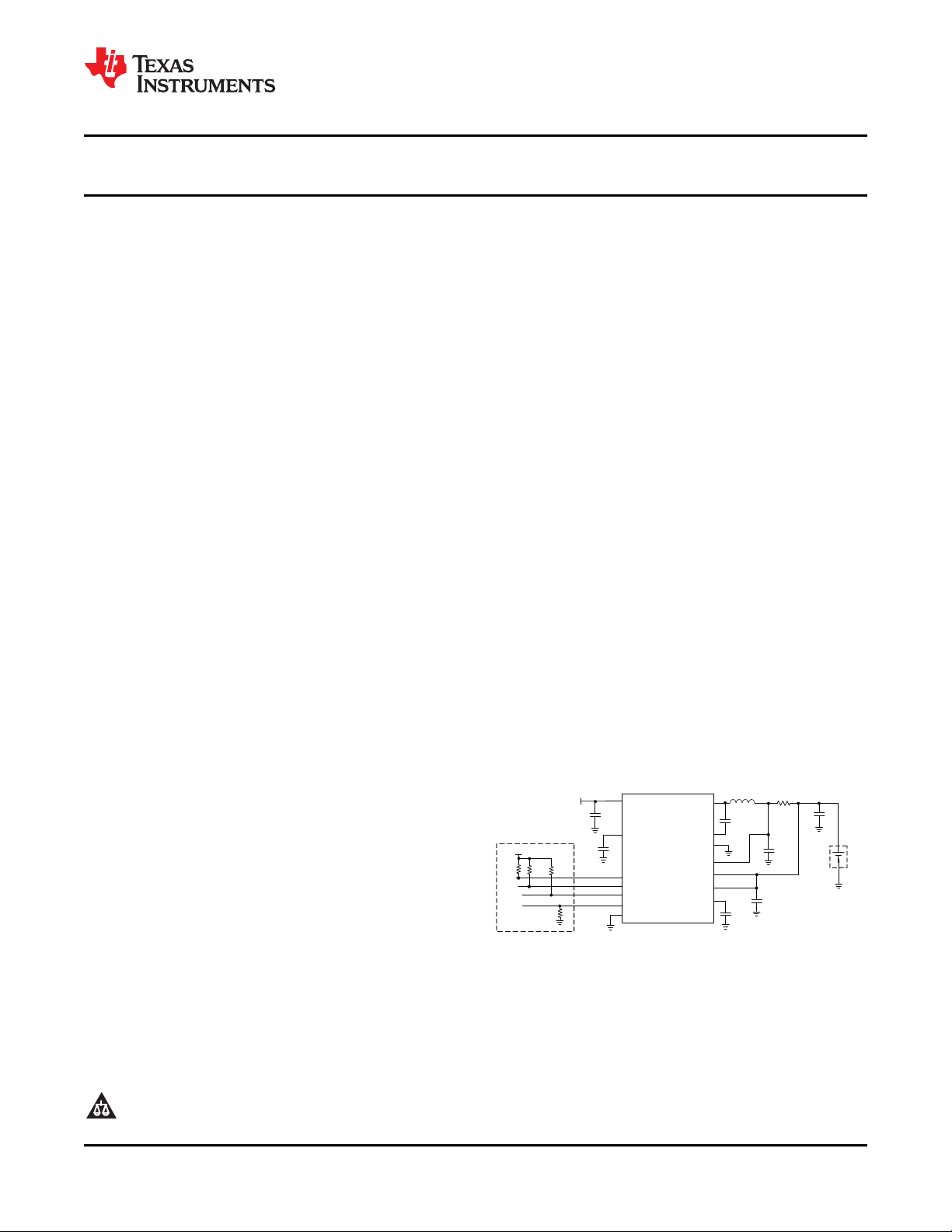
Typical Application Circuit
1
2I
PRODUCTION DATA information is current as of publication date.
Products conform to specifications per the terms of the Texas
Instruments standard warranty. Production processing does not
necessarily include testing of all parameters.
2
Please be aware that an important notice concerning availability, standard warranty, and use in critical applications of Texas
Instruments semiconductor products and disclaimers thereto appears at the end of this data sheet.
C is a trademark of Philips Electronics.
Copyright © 2010, Texas Instruments Incorporated
Page 2
3
2
1 14
7 8
4
6
5
11
12
13
9
10
PMID
Thermal
Pad
SW
PGND
SGND
BOOT
VBUS
CSIN
AUXPWR VREF
SCL
SDA
STAT
ISEL
CSOUT
bq24155
SLUS942 –FEBRUARY 2010
www.ti.com
This integrated circuit can be damaged by ESD. Texas Instruments recommends that all integrated circuits be handled with
appropriate precautions. Failure to observe proper handling and installation procedures can cause damage.
ESD damage can range from subtle performance degradation to complete device failure. Precision integrated circuits may be more
susceptible to damage because very small parametric changes could cause the device not to meet its published specifications.
DESCRIPTION CONTINUED
During the charging process, the bq24155 monitors its junction temperature (TJ) and reduces the charge current
once TJincreases to approximately 125°C. The bq24155 is available in 14-pin QFN package.
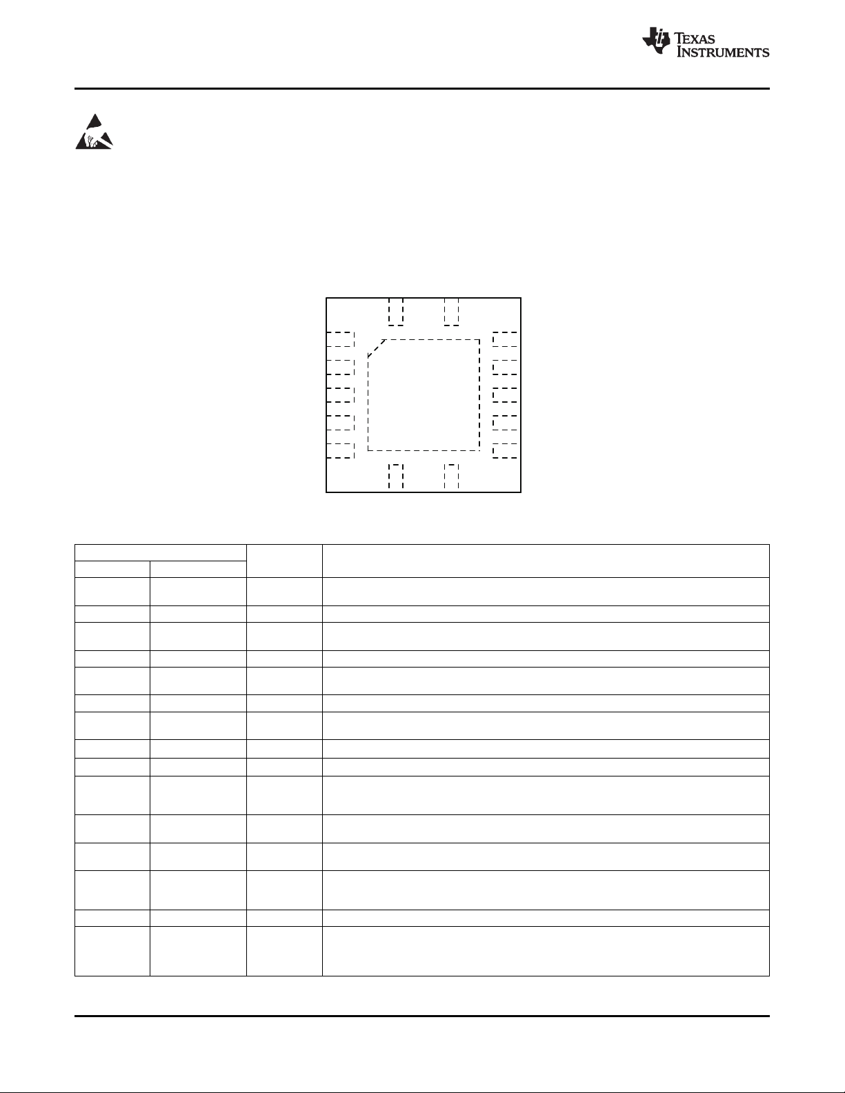
RGY PACKAGE
(Top View)
TERMINAL FUNCTIONS
TERMINAL
NAME NO.
CSOUT 6 I
VBUS 14 I Charger input voltage. Bypass it with a 1-mF ceramic capacitor from VBUS to PGND.
PMID 13 O
SW 12 O Internal switch to output inductor connection.
BOOT 1 O
PGND 11 Power ground
CSIN 9 I
SCL 2 I
SDA 3 I/O
STAT 4 O 128mS pulse is sent out. STAT pin can be disabled by the EN_STAT bit in control register. STAT can
VREF 8 O
AUXPWR 7 I
ISEL 5 I current limiting selection pin. When ISEL = High, Iin – limit = 500 mA and when ISEL = Low, Iin – limit
SGND 10 - Signal ground
Thermal pad pad -
2 Submit Documentation Feedback Copyright © 2010, Texas Instruments Incorporated
I/O DESCRIPTION
Battery voltage and current sense input. Bypass it with a ceramic capacitor (minimum 0.1 mF) to
PGND if there are long inductive leads to battery.
Connection point between reverse blocking FET and high-side switching FET. Bypass it with a
minimum of 3.3-mF capacitor from PMID to PGND.
Bootstrap capacitor connection for the high-side FET gate driver. Connect a 10-nF ceramic capacitor
(voltage rating above 10 V) from BOOT pin to SW pin.
Charge current-sense input. Battery current is sensed across an external sense resistor. A 0.1-mF
ceramic capacitor to PGND is required.
I2C interface clock. Open drain output, connect a 10-kΩ pullup resistor to 1.8V rail
I2C interface data. Open drain output, connect a 10-kΩ pullup resistor to 1.8V rail
Charge status pin. Pull low when charge in progress. Open drain for other conditions. During faults, a
be used to drive a LED or communicate with a host processor.
Internal bias regulator voltage. Connect a 1-mF ceramic capacitor from this output to PGND. External
load on VREF is not allowed.
Auxiliary power supply, connected to the battery pack to provide power in high-impedance mode.
Bypass it with a 1-mF ceramic capacitor from this pin to PGND.
Input current limiting selection pin. In 32 minutes mode, the ISEL pin is default to be used as the input
= 100 mA, see the Control Register for details.
There is an internal electrical connection between the exposed thermal pad and the PGND pin of the
device. The thermal pad must be connected to the same potential as the PGND pin on the printed
circuit board. Do not use the thermal pad as the primary ground input for the device. PGND/SGND
must be connected to ground at all times.
Product Folder Link(s): bq24155
Page 3
bq24155
www.ti.com
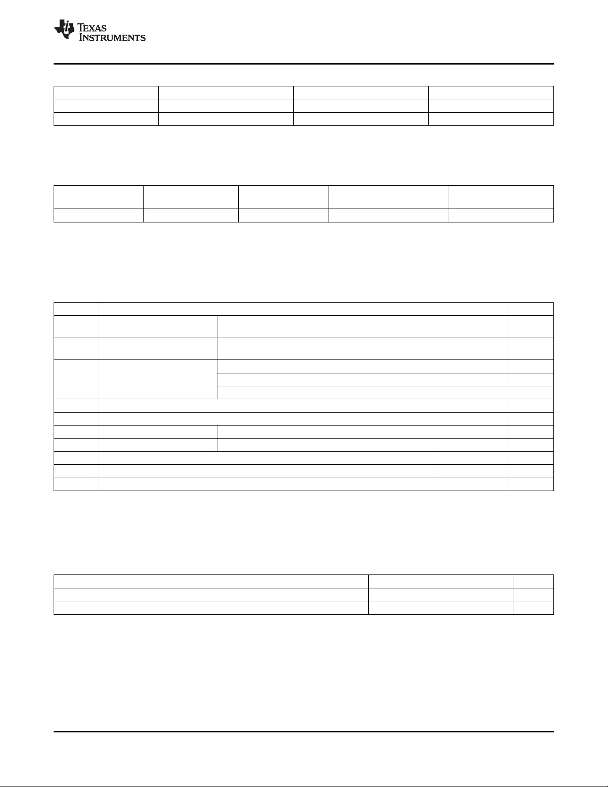
ORDERING INFORMATION
(1)
SLUS942 –FEBRUARY 2010
Part NO. MARKING MEDIUM QUANTITY
bq24155RGYR bq24155 Tape and Reel 3000
bq24155RGYT bq24155 Tape and Reel 250
(1) For the most current package and ordering information, see the Package Option Addendum at the end of this document, or see the TI
website at www.ti.com.
DISSIPATION RATINGS
PACKAGE R
QFN-14
(1)
(1)
qJA
55°C/W
R
qJC
(2)
15°C/W 1.82 W 0.018 W/°C
TA≤ 25°C DERATING FACTOR
POWER RATING TA> 25°C
(1) Maximum power dissipation is a function of TJ(max), RqJAand TA. The maximum allowable power dissipation at any allowable ambient
temperature is PD= [TJ(max)-TA] / RqJA.
(2) This data is based on using a JEDEC High-K 4-layer board and the exposed die pad is connected to a Cu pad on the board. The pad is
connected to the ground plane by a via matrix.
ABSOLUTE MAXIMUM RATINGS
(1) (2)
over operating free-air temperature range (unless otherwise noted)
VALUE UNIT
V
SS
V
I
Supply voltage range (with
respect to PGND)
Input voltage range (with
respect to and PGND)
VBUS –0.3 to 20
SCL, SDA, ISEL, CSIN, CSOUT, AUXPWR –0.3 to 7 V
PMID, STAT –0.3 to 20 V
V
O
Output voltage range (with
respect to and PGND)
VREF 6.5 V
SW, BOOT –0.7 to 20 V
Voltage difference between CSIN and CSOUT inputs (V
Voltage difference between BOOT and SW inputs (V
(BOOT)-V(SW)
(CSIN)-V(CSOUT)
) ±7 V
) –0.3 to 7 V
Output sink STAT 10 mA
I
O
T
A
T
J
T
stg
Output current (average) SW 1.25 A
Operating free-air temperature range –40 to 85 °C
Junction temperature –40 to 150 °C
Storage temperature –65 to 150 °C
(1) Stresses beyond those listed under absolute maximum ratings may cause permanent damage to the device. These are stress ratings
only, and functional operation of the device at these or any other conditions beyond those indicated under recommended operating
conditions is not implied. Exposure to absolute-maximum-rated conditions for extended periods may affect device reliability. All voltage
values are with respect to the network ground terminal unless otherwise noted.
(2) All voltages are with respect to PGND if not specified. Currents are positive into, negative out of the specified terminal.
(3) The bq24155 family can withstand up to 10.6 V continuously and 20 V for a minimum of 432 hours.
(3)
V
RECOMMENDED OPERATING CONDITIONS
MIN NOM MAX UNIT
V
BUS
T
J
Supply voltage, VBUS 4 6
Operating junction temperature range 0 +125 °C
(1) The inherent switching noise voltage spikes should not exceed the absolute maximum rating on either the BOOT or SW pins. A tight
layout minimizes switching noise.
Copyright © 2010, Texas Instruments Incorporated Submit Documentation Feedback 3
Product Folder Link(s): bq24155
(1)
V
Page 4
bq24155
SLUS942 –FEBRUARY 2010
www.ti.com
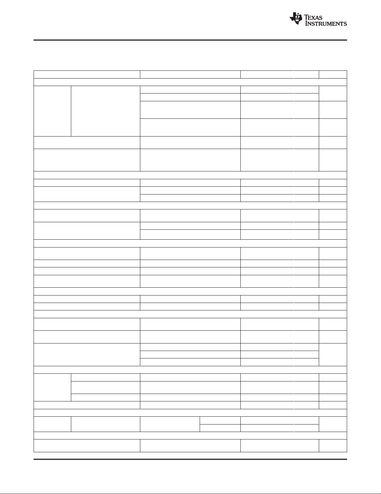
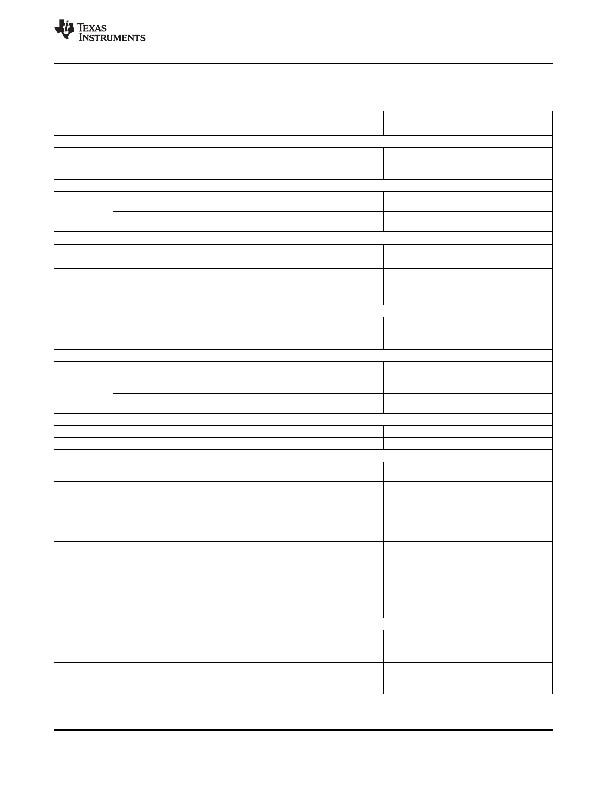
ELECTRICAL CHARACTERISTICS
Circuit of Figure 1, VBUS = 5 V, HZ_MODE = 0, OPA_MODE = 0 (charger mode operation), TJ= 0°C to 125°C, TJ= 25°C for
typical values (unless otherwise noted)
PARAMETER TEST CONDITIONS MIN TYP MAX UNIT
INPUT CURRENTS
VBUS > VBUS(min), PWM switching 10 mA
VBUS > VBUS(min), PWM NOT switching 5
0°C < TJ< 85°C, VBUS = 5 V, HZ_MODE = 1,
I
(VBUS)
VBUS supply current control
V
1.8 V
0°C < TJ< 85°C, VBUS = 5 V, HZ_MODE = 1,
V
= 0 V or 1.8 V
I
lkg
Leakage current from battery to 0°C < TJ< 85°C, V
VBUS pin impedance mode
Battery discharge current in High
Impedance mode, (CSIN, 20 mA
CSOUT, AUXPWR, SW pins)
0°C < TJ< 85°C, V
impedance mode,
VBUS = 0 V,
SCL, SDA, ISEL = 0 V or 1.8 V
VOLTAGE REGULATION
V
(OREG)
Output charge voltage Operating in voltage regulation, programmable 3.5 4.44 V
Voltage regulation accuracy
TA= 25°C –0.5% 0.5%
CURRENT REGULATION (FAST CHARGE)
I
O(CHARGE)
Output charge current V
programmable range R
Regulation accuracy for charge 20 mV ≤ V
current across R
V
(IREG)
= I
O(CHARGE)
(SNS)
× R
(SNS)
40 mV < V
WEAK BATTERY DETECTION
V
(LOWV)
Weak battery voltage threshold Programmable 3.4 3.7 V
programmable range
Weak battery voltage accuracy –5% 5%
Hysteresis for V
(LOWV)
Battery voltage falling 100 mV
Deglitch time for weak battery Rising voltage, 2 mV overdrive, t
threshold
ISEL PIN LOGIC LEVEL
V
IL
V
IH
Input low threshold level 0.4 V
Input high threshold level 1.3 V
CHARGE TERMINATION DETECTION
I
(TERM)
Termination charge current V
programmable range VBUS> V
Deglitch time for charge Both rising and falling, 2 mV overdrive, t
termination = 100 ns
Voltage regulation accuracy for
termination current across R
V
(IREG_TERM)
= I
O(TERM)
× R
(SNS)
(SNS)
3.4 mV ≤ V
6.8 mV ≤ V
13.6 mV ≤ V
INPUT POWER SOURCE DETECTION
Input voltage lower limit Input power source detection, Input voltage falling 3.6 3.8 4 V
VIN(min) Rising voltage, 2 mV overdrive, t
Deglitch time for VBUS rising ms
above VIN(min)
Hysteresis for VIN(min) Input voltage rising 100 200 mV
t
INT
Detection Interval Input power source detection 2 S
INPUT CURRENT LIMITING
I
IN
Input current limiting threshold USB charge mode
VREF BIAS REGULATOR
V
REF
Internal bias regulator voltage 2 6.5
VBUS >VIN(min) or V
I(VREF) = 1 mA, C(VREF) = 1 mF
> V
(AUXPWR)
(AUXPWR)
(LOWV)
(SNS)
(AUXPWR)
(LOWV)
< V
(LOWV)
≤ V
(AUXPWR)
= 68 mΩ Programmable
≤ 40 mV –5% 5%
(IREG)
(IREG)
> V
(OREG)
, R
(SLP)
(SNS)
(IREG_TERM)
(IREG_TERM)
(IREG_TERM)
, SCL, SDA, ISEL = 0 V or 20 mA
, 32 S mode, SCL, SDA, ISEL 35 mA
= 4.2 V, High
(AUXPWR)
(AUXPWR)
= 4.2 V, High
5 mA
–1% 1%
< V
(OREG)
, VBUS > V
, 550
(SLP)
1250 mA
–3% 3%
= 100 ns
RISE
– V
, mA
(RCH)
= 68 mΩ Programmable
, t
RISE
FALL
50 400
30 ms
30 ms
< 6.8 mV –25% 25%
< 13.6 mV –10% 10%
≤ 27.2 mV –5% 5%
= 100 ns 30
RISE
IIN= 100 mA 88 93 98 mA
IIN= 500 mA 450 475 500
> V
(AUXPWR)
min, V
(BAT)
4 Submit Documentation Feedback Copyright © 2010, Texas Instruments Incorporated
Product Folder Link(s): bq24155
Page 5
bq24155
www.ti.com
SLUS942 –FEBRUARY 2010
ELECTRICAL CHARACTERISTICS (continued)
Circuit of Figure 1, VBUS = 5 V, HZ_MODE = 0, OPA_MODE = 0 (charger mode operation), TJ= 0°C to 125°C, TJ= 25°C for
typical values (unless otherwise noted)
PARAMETER TEST CONDITIONS MIN TYP MAX UNIT
V
output short current limit 30 mA
REF
BATTERY RECHARGE THRESHOLD
V
(RCH)
STAT OUTPUTS
V
OL(STAT)
I2C BUS LOGIC LEVELS AND TIMING CHARACTERISTICS
V
OL
V
IL
V
IH
I
(BIAS)
f
(SCL)
BATTERY DETECTION
I
(DETECT)
SLEEP COMPARATOR
V
(SLP)
V
(SLP_EXIT)
UNDERVOLTAGE LOCKOUT
UVLO IC active threshold voltage VBUS rising 3.05 3.3 3.55 V
UVLO
(HYS)
PWM
f
(OSC)
D
(MAX)
D
(MIN)
CHARGE MODE PROTECTION
V
(OVP-IN)
V
(OVP)
Recharge threshold voltage Below V
Deglitch time 130 ms
Low-level output saturation
voltage, STAT
High-level leakage current for
STAT
(OREG)
V
t
decreasing below threshold,
(AUXPWR)
= 100ns, 10 mV overdrive
FALL
IO= 10 mA, sink current 0.4 V
Voltage on STAT pin is 5 V 1 mA
100 120 150 mV
Output low threshold level IO= 10 mA, sink current 0.4 V
Input low threshold level 0.4 V
Input high threshold level 1.2 V
Input bias current V
= 1.8 V, SDA and SCL 1 mA
(pull-up)
SCL clock frequency 3.4 MHz
Battery detection current before Begins after termination detected,
charge done (sink current)
(1)
V
(AUXPWR)
≤ V
(OREG)
–0.45 mA
Battery detection time 262 ms
Sleep-mode entry threshold,
V
- V
BUS
AUXPWR
Sleep-mode exit hysteresis 2.3 V ≤ V
Deglitch time for VBUS rising
above V
(SLP)
+ V
(SLP_EXIT)
2.3 V ≤ V
(AUXPWR)
(AUXPWR)
≤ V
≤ V
(OREG)
(OREG)
, V
BUS
Rising voltage, 2-mV overdrive, t
falling 0 40 100 mV
40 100 160 mV
= 100ns 30 ms
RISE
IC active hysteresis VBUS falling from above UVLO 120 150 mV
Voltage from BOOT pin to SW
pin
Internal top reverse blocking FET I
on-resistance PMID
Internal top N-channel Switching
FET on-resistance
Internal bottom N-channel FET
on-resistance
During charge or boost operation 6.5 V
= 500 mA, Measured from VBUS to
IN(LIMIT)
Measured from PMID to SW, V
- VSW= 4 V 120 250 mΩ
BOOT
180 250
Measured from SW to PGND 110 200
Oscillator frequency 3 MHz
Frequency accuracy –10% 10%
Maximum duty cycle 99.5%
Minimum duty cycle 0
Synchronous mode to
non-synchronous mode transition Low side FET cycle by cycle current sensing 100 mA
current threshold
Input VBUS OVP threshold Threshold over VBUS to turn off converter during
voltage charge
V
(OVP_IN)
Output OVP threshold voltage 110 117 121
V
hysteresis Lower limit for V
(OVP)
(2)
hysteresis VBUS falling from above V
V
threshold over V
(CSOUT)
during charge
falling from above V
(CSOUT)
(OVP_IN)
to turn off charger
(OREG)
(OVP)
6.3 6.5 6.7 V
140 mV
%V
11
(OREG)
(1) Negative charge current means the charge current flows from the battery to charger (discharging battery).
(2) Bottom N-channel FET always turns on for Ⅹ60 ns and then turns off if current is too low.
Copyright © 2010, Texas Instruments Incorporated Submit Documentation Feedback 5
Product Folder Link(s): bq24155
Page 6
C
VREF
10 nF
C
BOOT
+
PACK
-
PACK
+
C
AUXPWR
SCL
SDA
CSOUT
CSIN
PGND
SW
I
2
CBUS
VAUX
HOST
SCL
SDA
STAT
VREF
STAT
PMID
VBUS
C
IN
V
BUS
C
IN
BOOT
ISEL
U1
AUXPWR
ISEL
C
O
R
SNS
C
CSIN
V
BAT
1 Fm
4.7 Fm
10kW
10kW
10kW
10kW
10kW
L 1.0 HOm
68mW
10 Fm
0.1 Fm
1 Fm
1 Fm
bq24155
SGND
bq24155
SLUS942 –FEBRUARY 2010
www.ti.com
ELECTRICAL CHARACTERISTICS (continued)
Circuit of Figure 1, VBUS = 5 V, HZ_MODE = 0, OPA_MODE = 0 (charger mode operation), TJ= 0°C to 125°C, TJ= 25°C for
typical values (unless otherwise noted)
PARAMETER TEST CONDITIONS MIN TYP MAX UNIT
I
(LIMIT)
V
(SHORT)
I
(SHORT)
PROTECTION
T
(SHTDWN)
T
(CF)
T
(32S)
(3) Verified by design
Cycle-by-cycle current limit for
charge
Short-circuit voltage threshold V
V
hysteresis V
(SHORT)
Short-circuit current V
Thermal trip 165
Thermal hysteresis 10 °C
Thermal regulation threshold
Time constant for the 32 second
timer
Charge mode operation 1.5 2.3 3 A
falling 1.9 2 2.1 V
(AUXPWR)
rising from below V
(AUXPWR)
≤ V
(AUXPWR)
(3)
Charge current begins to reduce 120
32 Second mode 12 32 s
(SHORT)
(SHORT)
5 10 15 mA
100 mV
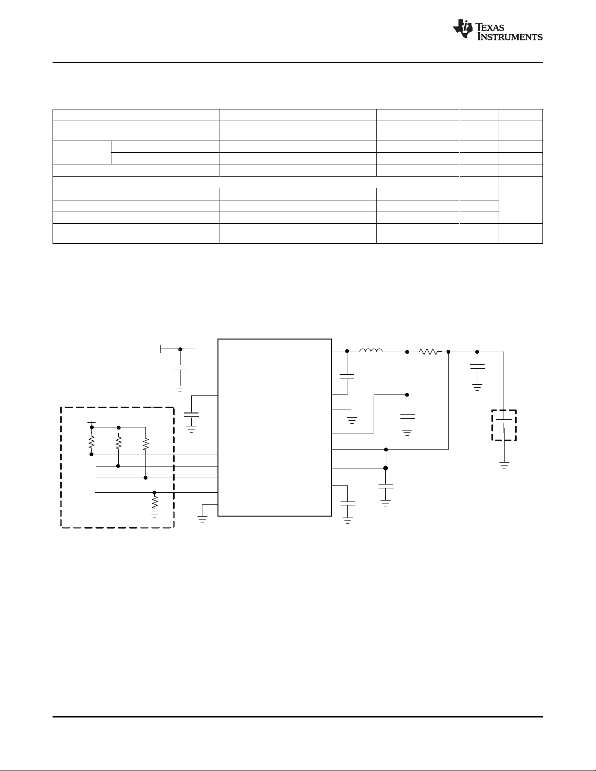
TYPICAL APPLICATION CIRCUITS
VBUS = 5 V, I
seconds.
(CHARGE)
= 1250 mA, VBAT = 3.5 V to 4.44 V (adjustable), Safety Timer = 32 minutes or 32
Figure 1. I2C Controlled 1-Cell Charger Application Circuit
VBUS = 5 V, I
(IN_LIMIT)
6 Submit Documentation Feedback Copyright © 2010, Texas Instruments Incorporated
= 500 mA, V
= 3.5 V to 4.44 V (adjustable), Safety Timer = 32 minutes or 32 seconds.
OUT
Product Folder Link(s): bq24155
Page 7
+
PACK
-
V
SYS
Host
-
Controlled
Switch
PACK
+
SCL
SDA
CSOUT
CSIN
PGND
SW
I
2
CBUS
VAUX
HOST
SCL
SDA
STAT
VREF
STAT
PMID
VBUS
C
IN
V
BUS
C
IN
1 Fm
BOOT
ISEL
U1
AUXPWR
C
VREF
C
O
C
BOOT
R
SNS
C
CSIN
1 Fm
C
AUXPWR
C
CSOUT
ISEL
10nF
68mW
V
OUT
4.7 Fm
10kW
10kW
10kW
10kW
10kW
LO1.0 Hm
0.1 Fm
10 Fm
0.1 Fm
1 Fm
bq24155
Host
Charge
Controller
Q
SGND
VBUS
2V/div
I
0.5 A/div
BAT
500 S/divm
Vbus=0–5V,Vbat=3.5VChargemode
VSW
5V/div
VBAT
2V/div
VSW
5V/div
I
0.5 A/div
BAT
1S/div
Vbus=5V,Iin_limit=500mA,
32SMode
VSW
2V/div
IL
0.5 A/div
Vbus=5V Vbat=2.6V,Voreg=4.2V,Ichg=1250mA,
100nS/div
VBUS
2V/div
VSW
5V/div
I
0.1 A/div
BUS
2mS/div
Vbus=5V@10mA,Iin_limit=100mA,
Vbat=3.2V,Ichg=550mA
bq24155
www.ti.com
TYPICAL APPLICATION CIRCUITS (continued)
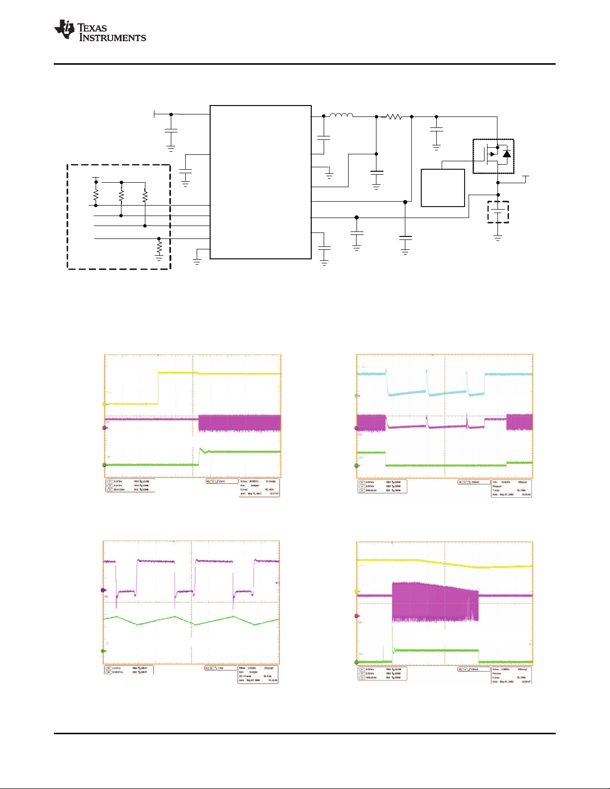
Figure 2. I2C Controlled 1-Cell Pre-Regulator Application
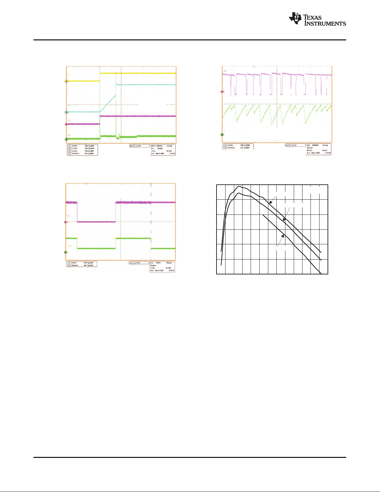
TYPICAL CHARACTERISTICS
Using circuit shown in Figure 1, TA= 25°C, unless otherwise specified.
ADAPTER INSERTION BATTERY INSERTION/REMOVAL
SLUS942 –FEBRUARY 2010
Figure 3. Figure 4.
PWM CHARGING WAVEFORMS POOR SOURCE DETECTION
Copyright © 2010, Texas Instruments Incorporated Submit Documentation Feedback 7
Figure 5. Figure 6.
Product Folder Link(s): bq24155
Page 8
VSW
2V/div
I
0.5 A/div
L
2 S/divm
Vbus=5V,Vbat=3.6VChargemode
operation
V
5V/div
BUS
V
1V/div
BAT
ISEL
5V/div
I
50mA/div
BAT
20mS/div
V =0-5V,
NoBattery,
C =100 F,
R =5k
IN
OUT
LOAD
m
W
ISEL
5V/div
I
0.2 A/div
BUS
0.5S/div
Vbus=5V,Iin_limit=100/500mA,
(ISEL Control,32MinuteMode),
Iin_limit=100mA (I CControl,32SecondMode)
2
32Minute
Mode
32Second
Mode
80
82
84
86
88
90
92
0 100 200 300 400 500 600 700 800 900 1000 1100 12001300
ChargeCurrent-mA
Efficiency-%
Vbat=4V
Vbat=3V
Vbat=3.6V
V =5V
BUS
bq24155
SLUS942 –FEBRUARY 2010
BATTERY DETECTION AT POWER UP CYCLE BY CYCLE CURRENT LIMIT IN CHARGE MODE
INPUT CURRENT CONTROL CHARGER EFFICIENCY
www.ti.com
TYPICAL CHARACTERISTICS (continued)
Figure 7. Figure 8.
Figure 9. Figure 10.
8 Submit Documentation Feedback Copyright © 2010, Texas Instruments Incorporated
Product Folder Link(s): bq24155
Page 9
SW
bq24155
CHARGECONTROL,
TIMERandDISPLAY
LOGIC
*
Sleep
CSOUT
CSIN
STAT
PGND
SW
PGND
SCL
NMOS
NMOS
NMOS
PMID
SDA
(I2CControl)
Decoder
DAC
Q2
Q3
VREF
PMID
Q1
BOOT
REFERNCES
& BIAS
PMID
VBUS
SW
V
PMID
PGND
VBUS
V
PMID
ISEL
AUXPWR
I
SHORT
VREF
LINEAR _CHG
+
-
-
+
-
-
+
-
+
-
T
J
T
CF
I
OCHARGE
V
OREG
VREF
Charge
Pump
VREF1
I
IN_
LIMIT
OSC
+
-
V
OVP
_IN
V
BUS
V
BUS
+
-
V
UVLO
V
BUS
+
V
IN(
MIN)
V
BUS
+
-
T
J
T
SHTDWN
CBC
Current
Limiting
PWM
Controller
I
LIMIT
+
-
V
BAT
V
BUS
VBAT
VOUT
VCSIN
*
BatteryOVP
+
-
V
OUT
V
OVP
VBUSUVLO
PoorInput
VBUSOVP
Thermal
Shutdown
*
Recharge
+
-
V
OUT
V
OREG-VRCH
*
SignalDeglitched
+
-
-
V
OUT
V
CSIN
I
TERM
*
PWM_CHG
*
PWMCharge
Mode
+
-
V
BAT
V
SHORT
Termination
VREF1
bq24155
www.ti.com
SLUS942 –FEBRUARY 2010
FUNCTIONAL BLOCK DIAGRAM (Charge Mode)
Copyright © 2010, Texas Instruments Incorporated Submit Documentation Feedback 9
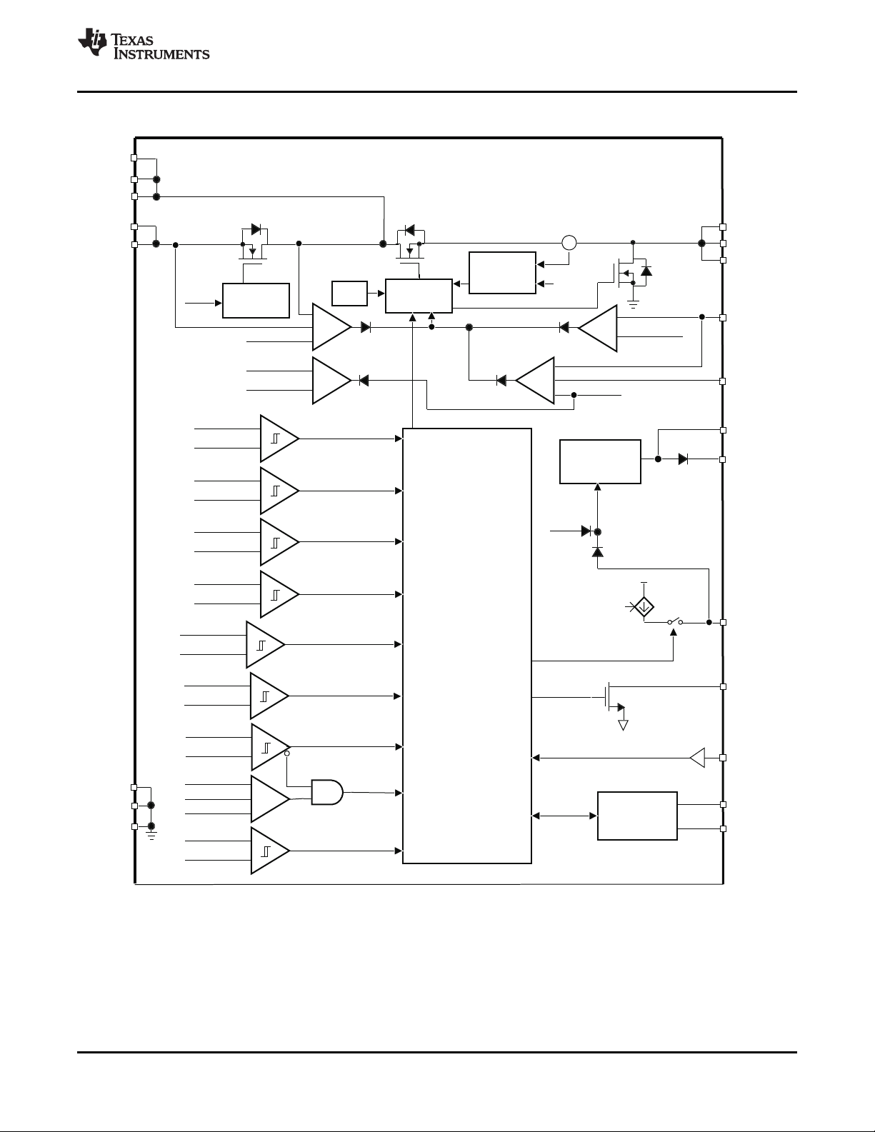
Figure 11. Function Block Diagram of bq24155 in Charge Mode
Product Folder Link(s): bq24155
Page 10
V
AUXPWR<VSHORT
?
Yes
No
32-Minute
TimerExpired?
No
EnableI
SHORT
IndicateCharge-In-
Progress
Regulate
InputCurrent, Charge
CurrentorVoltage
HighImpedanceModeorHost
ControlledOperationMode
TerminationEnabled
I
TERM
detected
andV
AUXPWR>VOREG-VRCH
?
Yes
V
AUXPWR
< V
OREG
-
V
RCH
?
V
AUXPWR<VSHORT
?
No
No
Yes
Yes
Yes
/CE=HIGH
TurnOffCharge
IndicateFault
IndicateShort
Circuitcondition
32-Minute
Timer Expired?
No
Yes
Yes
IndicateDONE
ChargeComplete
V
BUS<VIN(MIN)
?
Yes
No
IndicatePower
notGood
DisableCharge
WaitMode
Delay T
INT
V
BUS<VIN(MIN)
?
No
Yes
V
AUXPWR
< V
OREG
-
V
RCH
?
EnableI
DETECT
for
t
DETECT
TurnOffCharge
No
No
ResetCharge
Parameters
BatteryRemoved
WaitMode
Delay T
INT
Yes
V
AUXPWR<VLOWV
and bq24155?
PowerUp
V
BUS>VUVLO
No
Yes
Any ChargeState/CE=HIGH
ChargeConfigure
Mode
DisableCharge
/CE=LOW
32-Minute Timer
Active?
No
Yes
HighImpedance
Mode
ChargeComplete
ResetandStart
32-MinuteTimer
POR
LoadI2CRegisters
withDefaultValue
bq24155
SLUS942 –FEBRUARY 2010
OPERATIONAL FLOW CHART
www.ti.com
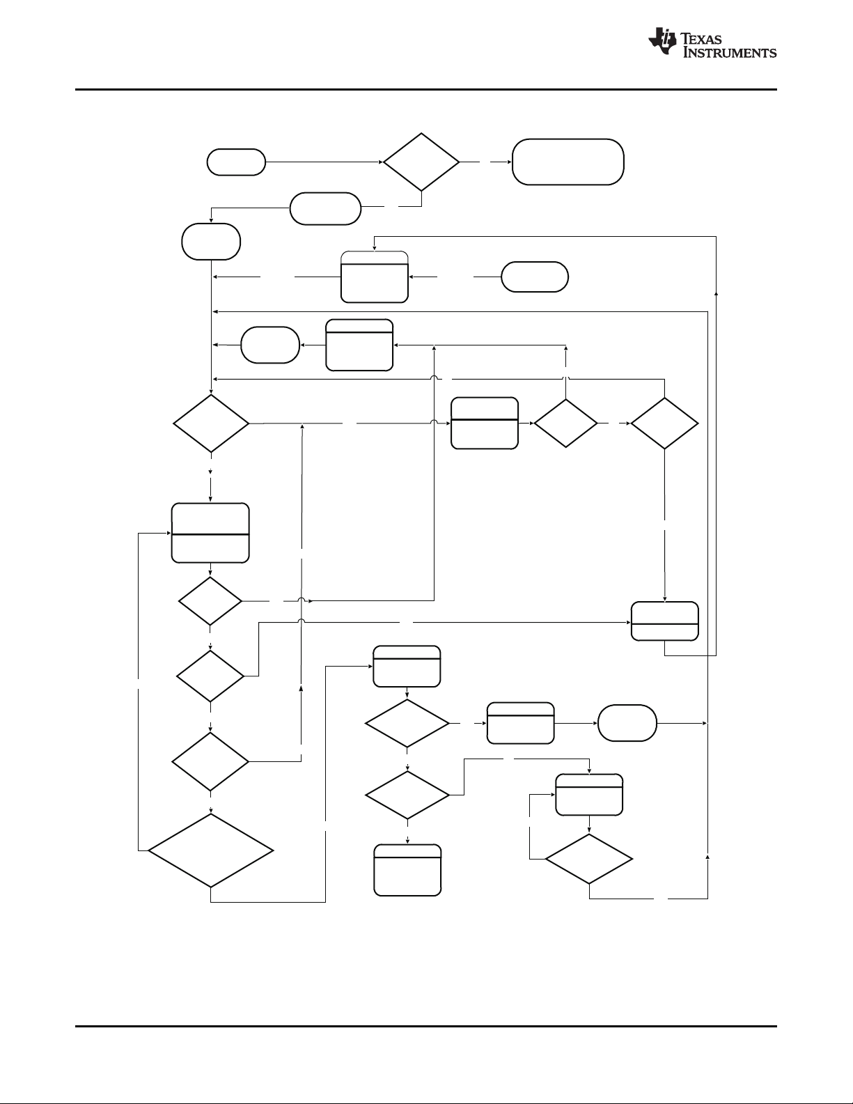
Figure 12. Operational Flow Chart of bq24155 in Charge Mode
10 Submit Documentation Feedback Copyright © 2010, Texas Instruments Incorporated
Product Folder Link(s): bq24155
Page 11

bq24155
www.ti.com
SLUS942 –FEBRUARY 2010
DETAILED FUNCTIONAL DESCRIPTION
For a current limited power source, such as a USB host or hub, a high efficiency converter is critical to fully use
the input power capacity for quickly charging the battery. Due to the high efficiency for a wide range of input
voltages and battery voltages, the switch mode charger is a good choice for high speed charging with less power
loss and better thermal management than a linear charger.
The bq24155 is a highly integrated synchronous switch-mode charger, featuring integrated FETs and small
external components, targeted at extremely space-limited portable applications powered by 1-cell Li-Ion or
Li-polymer battery pack.
The bq24155 has two operation modes: charge mode and high impedance mode. In charge mode, the bq24155
supports a precision Li-ion or Li-polymer charging system for single-cell applications. In high impedance mode,
the bq24155 stops charging and operates in a mode with low current from VBUS or battery, to effectively reduce
the power consumption when the portable device in standby mode. Through the proper control, bq24155
achieves the smooth transition among the different operation modes.
CHARGE MODE OPERATION
Charge Profile
In charge mode, bq24155 has four control loops to regulate input current, charge current, charge voltage and
device junction temperature, as shown in Figure 11. During the charging process, all four loops are enabled and
the one that is dominant takes control. The bq24155 supports a precision Li-ion or Li-polymer charging system
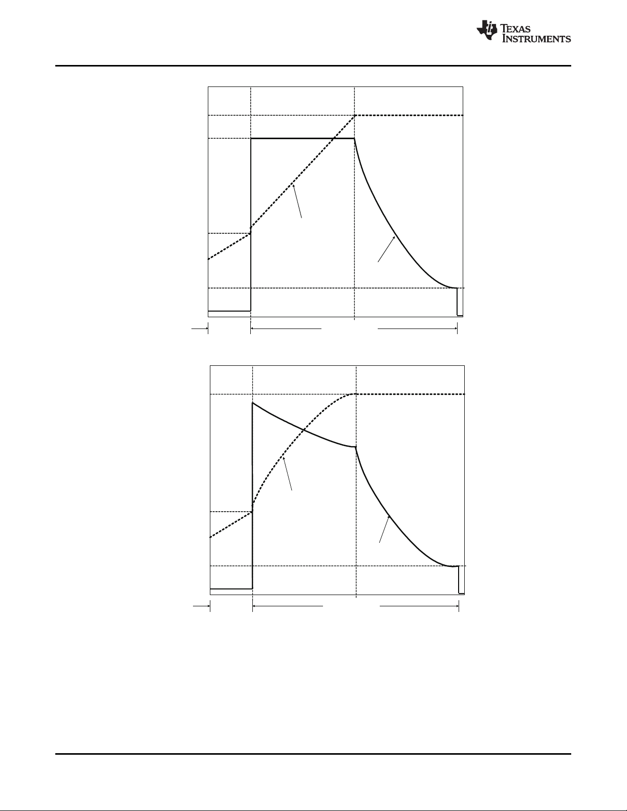
for single-cell applications. Figure 13(a) indicates a typical charge profile without input current regulation loop. It
is the traditional CC/CV charge curve, while Figure 13(b) shows a typical charge profile when input current
limiting loop is dominant during the constant current mode. In this case, the charge current is higher than the
input current so the charge process is faster than the linear chargers. For bq24155, the input current limits, the
charge current, termination current, and charge voltage are all programmable using I2C interface.
Copyright © 2010, Texas Instruments Incorporated Submit Documentation Feedback 11
Product Folder Link(s): bq24155
Page 12
Precharge
(LinearCharge)
FastCharge
(PWMCharge)
I
SHORT
Termination
V
SHORT
Regulation
Current
Regulation
Voltage
Precharge
Phase
CurrentRegulation
Phase
VoltageRegulation
Phase
ChargeCurrent
ChargeVoltage
Precharge
(LinearCharge)
FastCharge
(PWMCharge)
I
SHORT
Termination
V
SHORT
Regulation
voltage
Precharge
Phase
CurrentRegulation
Phase
VoltageRegulation
Phase
ChargeCurrent
ChargeVoltage
(a)
(b)
bq24155
SLUS942 –FEBRUARY 2010
www.ti.com
Figure 13. Typical Charging Profile of bq24155 for (a) without Input Current Limit, and (b) with Input
Current Limit
12 Submit Documentation Feedback Copyright © 2010, Texas Instruments Incorporated
Product Folder Link(s): bq24155
Page 13

bq24155
www.ti.com
SLUS942 –FEBRUARY 2010
PWM Controller in Charge Mode
The bq24155 provides an integrated, fixed 3-MHz frequency voltage-mode controller with Feed-Forward function
to regulate charge current or voltage. This type of controller is used to improve line transient response, thereby,
simplifying the compensation network used for both continuous and discontinuous current conduction operation.
The voltage and current loops are internally compensated using a Type-III compensation scheme that provides
enough phase margin for stable operation, allowing the use of small ceramic capacitors with low ESR. The
device operates between 0% to 99.5% duty cycles.
The bq24155 has back to back common-drain N-channel FETs at the high side and one N-channel FET at low
side. The input N-FET (Q1) prevents battery discharge when VBUS is lower than VAUXPWR. The second
high-side N-FET (Q2) is the switching control switch (see Figure 11). A charge pump circuit is used to provide
gate drive for Q1, while a bootstrap circuit with an external bootstrap capacitor is used to supply the gate drive
voltage for Q2.
Cycle-by-cycle current limit is sensed through the FETs Q2 and Q3. The threshold for Q2 is set to a nominal
2.3-A peak current. The low-side FET (Q3) also has a current limit that decides if the PWM Controller will operate
in synchronous or non-synchronous mode. This threshold is set to 100mA and it turns off the low-side N-channel
FET (Q3) before the current reverses, preventing the battery from discharging. Synchronous operation is used
when the current of the low-side FET is greater than 100mA to minimize power losses.
Battery Charging Process
At the beginning of precharge, while battery voltage is below the V
short-circuit current, I
(SHORT)
When the battery voltage is above V
current, I
O(CHARGE)
, or a charge current that corresponds to the input current of I
, to the battery.
(SHORT)
and below V
, the charge current ramps up to fast charge
(OREG)
(SHORT)
threshold, the bq24155 applies a
(IN_LIMIT)
. The slew rate for fast
charge current is controlled to minimize the current and voltage over-shoot during transient. Both the input
current limit (default at 100 mA), IIN_LIMIT, and fast charge current, I
battery voltage reaches the regulation voltage, V
, the charge current is tapered down as shown in
(OREG)
O(CHARGE)
, can be set by the host. Once the
Figure 13. The voltage regulation feedback occurs by monitoring the battery-pack voltage between the CSOUT
and PGND pins. The regulation voltage is adjustable (3.5 V to 4.44 V) and it is programmed through I2C
interface.
The bq24155 monitors the charging current during the voltage regulation phase. Once the termination threshold,
ITERM, is detected and the battery voltage is above the recharge threshold, the bq24155 terminates charge. The
termination current level is programmable. To disable the charge current termination, the host can set the charge
termination bit (I_Term) of charge control register to 0, see the I2C section for details.
A new charge cycle is initiated when one of the following conditions is detected:
• The battery voltage falls below the V
• VBUS Power-on reset (POR), if battery voltage is below the V
(OREG)
– V
(RCH)
threshold.
(LOWV)
threshold.
• CE bit toggle or RESET bit is set (host controlled)
Safety Timer in Charge Mode
At the beginning of charging process, the bq24155 starts a 32-minute timer (T32min) that can be stopped by any
write-action performed by host through I2C interface. Once the 32-minute timer is stopped, a 32-second timer
(T32sec) is automatically started. The 32-second timer can be reset by host using I2C interface. Writing "1" to
reset bit of TMR_RST in control register resets the 32-second timer and TMR_RST is automatically set to "0"
after the 32-second timer is reset. If the 32-second timer expires, the charge is terminated and charge
parameters are reset to default values. Then the 32-minute timer starts and the charge resumes.
During normal charging process, the bq24155 is normally in 32-second mode with host control, and 32-minute
mode without host control using I2C interface. The process repeats until the battery is fully charged. If the
32-minute timer expires, bq24155 turns off the charger, enunciates FAULT on the STATx bits of status register,
and sends the 128µs interrupt pulse. This function prevents battery over charge if the host fails to reset the
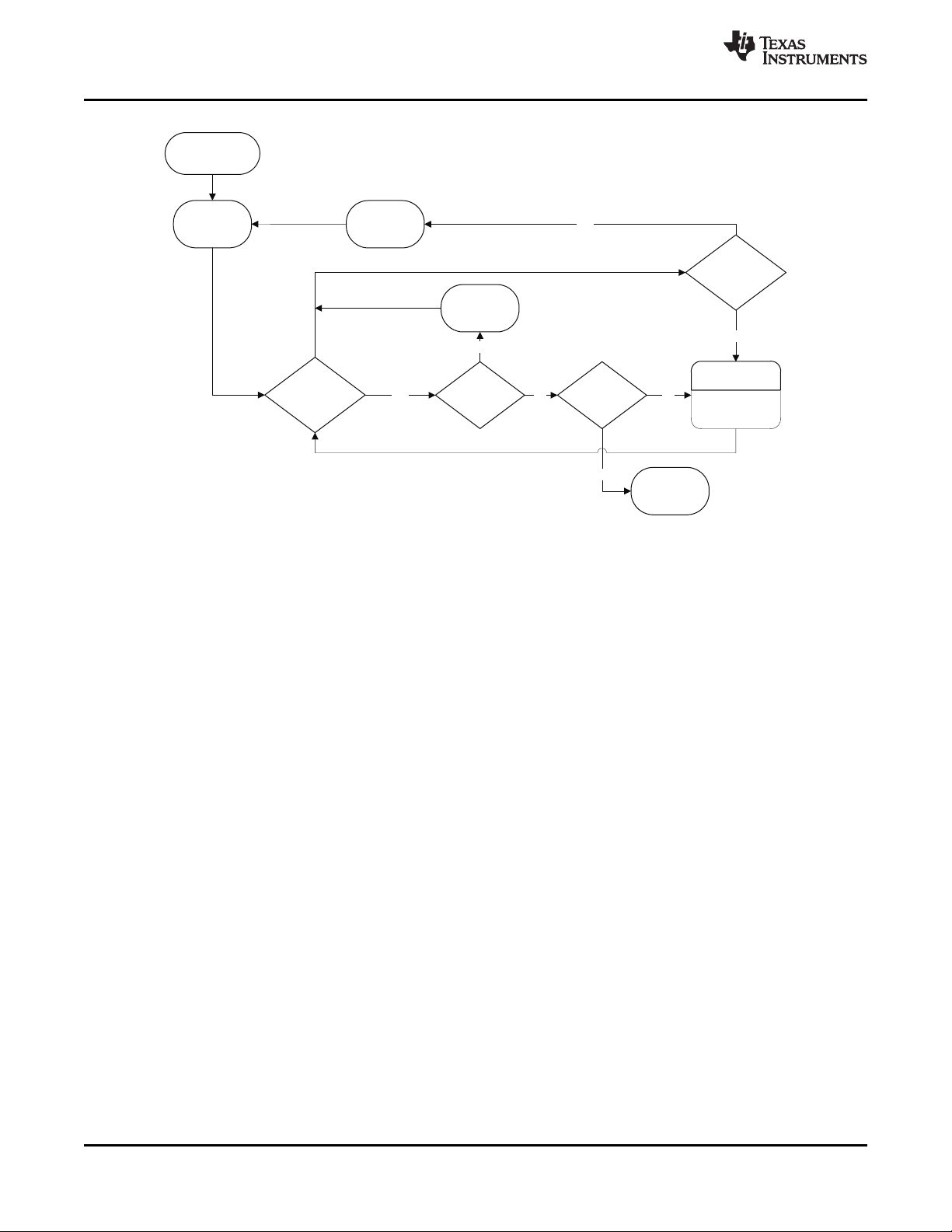
safety timer. The safety timer flow chart is shown in Figure 14. Fault condition is cleared by POR and fault status
bits can only be updated after the status bits are read out by the host.
Copyright © 2010, Texas Instruments Incorporated Submit Documentation Feedback 13
Product Folder Link(s): bq24155
Page 14
T32min Active?
Yes
No
Charge
HostShouldReset
T32sec Timer
T32min
Expired?
Start T32min
Timer
ChargeStart
No
TimerFault
Yes
T32secExpired?
Yes
No
ResetCharge
Parameters
AnyI2CWrite-
Action?
Yes
Start T32sec
Stop T32min
No
bq24155
SLUS942 –FEBRUARY 2010
www.ti.com
Figure 14. Timer Flow Chart for bq24155 in Charge Mode
USB Friendly Boot-Up Sequence
At power on reset (POR) of VBUS, if the battery voltage is above the weak battery threshold, V
operates in a mode dictated by the I2C control registers. On the other hand, if the battery voltage is below V
LOWV
, bq24155
LOWV
and the host control through I2C interface is lost (32 minute mode), bq24155 resets all I2C registers with default
values and enables the charger with an input current limit dictated by the ISEL pin voltage level until the host
programs the I2C registers. During this period, the input current limit is 100 mA when the voltage level of ISEL
pin is Low; while the input current limit is 500 mA when the voltage level of ISEL pin is high. This feature could
quickly revive a deeply discharged cell. The charge process continues after the battery is charged to the
regulation voltage (default at 3.54 V) since termination is disabled by default. In another case, if the battery
voltage is below V
but the host control using I2C interface is available (32 second mode), bq24155 operates
LOWV
in a mode dictated by control registers.
Input Current Limiting
To maximize the charge rate of bq24155 without overloading the USB port, the input current for bq24155 can be
limited to 100mA or 500mA which is programmed in the control register or ISEL pin. Once the input current
reaches the input current limiting threshold, the charge current is reduced to prevent the input current from
exceeding the programmed threshold. For bq24155, the default input current limit is controlled by the ISEL pin at
VBUS power on reset when V
(AUXPWR)
is lower than V
. The input current sensing resistor and control loop
(LOWV)
are integrated into bq24155. The input current limit can also be disabled using I2C control, see the definition of
control register (01H) for details.
Thermal Regulation and Protection
To prevent overheating the chip during the charging process, the bq24155 monitors the junction temperature, TJ,
of the die and begins to taper down the charge current once TJreaches the thermal regulation threshold, TCF.
The charge current is reduced to zero when the junction temperature increases approximately 10°C above TCF.
At any state, if TJexceeds T
and all timers are frozen. Charging resumes when TJfalls below T
SHTDWN
, bq24155 suspends charging. At thermal shutdown mode, PWM is turned off
SHTDWN
by approximately 10°C.
14 Submit Documentation Feedback Copyright © 2010, Texas Instruments Incorporated
Product Folder Link(s): bq24155
Page 15

bq24155
www.ti.com
SLUS942 –FEBRUARY 2010
Input Voltage Protection in Charge Mode
Sleep Mode
The bq24155 enters the low-power sleep mode if the voltage on VBUS pin falls below sleep-mode entry
threshold, V
AUXPWR
+ V
, and VBUS is still higher than the poor source detection threshold, VIN(min). This
SLP
feature prevents draining the battery during the absence of VBUS. During sleep mode, both the reverse blocking
switch Q1 and PWM are turned off.
Input Source Detection
During the charging process, bq24155 continuously monitors the input voltage, VBUS. If VBUS falls to the low
input voltage threshold, VIN(min), poor input power source is detected. Under this condition, bq24155 terminates
the charge process, waits for a delay time of T
and repeats the charging process, as indicated in Figure 12.
INT
This unique function provides intelligence to bq24155 and so prevents USB power bus collapsing and oscillation
when connecting to a suspended USB port, or a USB-OTG device with low current capability.
Input Overvoltage Protection
The bq24155 provides a built-in input over-voltage protection to protect the device and other components against
damages if the input voltage (Voltage from VBUS to PGND) goes too high. When an input overvoltage condition
is detected, bq24155 turns off the PWM converter, sets fault status bits, and sends out fault pulse in STAT pin.
Once VBUS drops below the input overvoltage exit threshold, the fault is cleared and charge process resumes.
Battery Protection in Charge Mode
Output Overvoltage Protection
The bq24155 provides a built-in overvoltage protection to protect the device and other components against
damage if the battery voltage goes too high, as when the battery is suddenly removed. When an overvoltage
condition is detected, bq24155 turns off the PWM converter, sets fault status bits and sends out fault pulse in
STAT pin. Once V
(CSOUT)
drops to the battery overvoltage exit threshold, the fault is cleared and charge process
back to normal.
Battery Detection During Normal Charging
For applications with removable battery packs, the bq24155 provides a battery absent detection scheme to
reliably detect insertion or removal of battery packs.
During normal charging process with host control, once the voltage at the AUXPWR pin is above the battery
recharge threshold, V
(OREG)
charge and enables a discharge current, I
– V
, and the termination charge current is detected, bq24155 turns off the
(RCH)
(DETECT)
, for a period of t
, then checks the battery voltage. If the
DETECT
battery voltage is still above recharge threshold, the battery is present and the charge done is detected.
However, if the battery voltage is below battery recharge threshold, the battery is absent. Under this condition,
the charge parameters (such as input current limit) are reset to the default values and charge resumes after a
delay of T
, as shown in Figure 12. This function ensures that the charge parameters are reset whenever the
INT
battery is replaced.
Power Up Without Battery
When no battery is present, at VBUS power up, bq24155 will charge the output capacitor in short circuit mode
(when V
AUXPWR<VSHORT
) or PWM mode (when V
AUXPWR>VSHORT
). Once the output voltage at CSOUT pin is
charged to the default regulation voltage (3.54V), the voltage is kept constant until the 32-minute timer expires or
the host takes over the control through I2C interface. This unique feature makes bq24155 capable of starting the
system without battery.
Battery Short Protection
During the normal charging process, if the battery voltage is lower than the short-circuit threshold, V
charger operates in short circuit mode with a lower charge rate of I
Copyright © 2010, Texas Instruments Incorporated Submit Documentation Feedback 15
Product Folder Link(s): bq24155
, as shown in Figure 13.
(SHORT)
(SHORT)
, the
Page 16
OUT OUT
1
=
o
2 L C
f
p ´ ´
bq24155
SLUS942 –FEBRUARY 2010
www.ti.com
Charge Status Output, STAT Pin
The STAT pin is used to indicate operation conditions for bq24155. STAT is pulled low during charging when
EN_STAT bit in control register (00H) is set to "1". Under other conditions, the STAT pin acts as a high
impedance (open-drain) output. Under fault conditions, a 128-ms pulse is sent out to notify the host. The status of
STAT pin at different operation conditions is summarized in Table 1. The STAT pin can be used to drive an LED
or communicate to the host processor.
Table 1. STAT Pin Summary
CHARGE STATE STAT
Charge in progress and EN_STAT = 1 Low
Other normal conditions Open-drain
Charge mode faults: Timer fault, sleep mode, VBUS 128-ms pulse, then open-drain
or battery overvoltage, poor input source, VBUS
UVLO, no battery, thermal shutdown
Control Bits in Charge Mode
CE Bit (Charge Mode)
The bit of CE in control register is used to disable or enable the charge process. A low logic level (0) on this bit
enables the charge and a high logic level (1) disables the charge.
RESET Bit
The bit of RESET in control register is used to reset all the charge parameters. Writing '1" to RESET bit resets all
the charge parameters to default values and RESET bit is automatically cleared to zero once the charge
parameters are reset. It is designed for charge parameter reset before charge starts, and it is not recommended
to set the RESET bit when charging or boosting in progress.
OPA_Mode Bit
OPA_MODE is the operation mode control bit. When OPA_MODE = 0, the bq24155 operates as a charger if
HZ_MODE is set to "0", refer to Table 2 for detail.
Table 2. Operation Mode Summary
OPA_MODE HZ_MODE OPERATION MODE
0 0 Charge (no fault)
1 0 NA
X 1 High impedance
Charge configure (fault, V
High impedance (V
bus
< V
bus
UVLO
> V
)
UVLO
)
High Impedance Mode
When control bit of HZ-MODE is set to "1", the bq24155 operates in high impedance mode, with the impedance
in VBUS pin higher than 165 kΩ. In high impedance mode, a crude 32-second timer is enabled when the battery
voltage is below V
to monitor the host control is available or not. If the crude 32 second timer expires, the
(LOWV)
bq24155 operates in 32 minute mode and the crude 32 second timer is disabled. In 32 minute mode, when
VBUS is below UVLO, the bq24155 operates in high impedance mode regardless of the setting of the HZ_MODE
bit.
Output Inductor and Capacitance Selection Guidelines
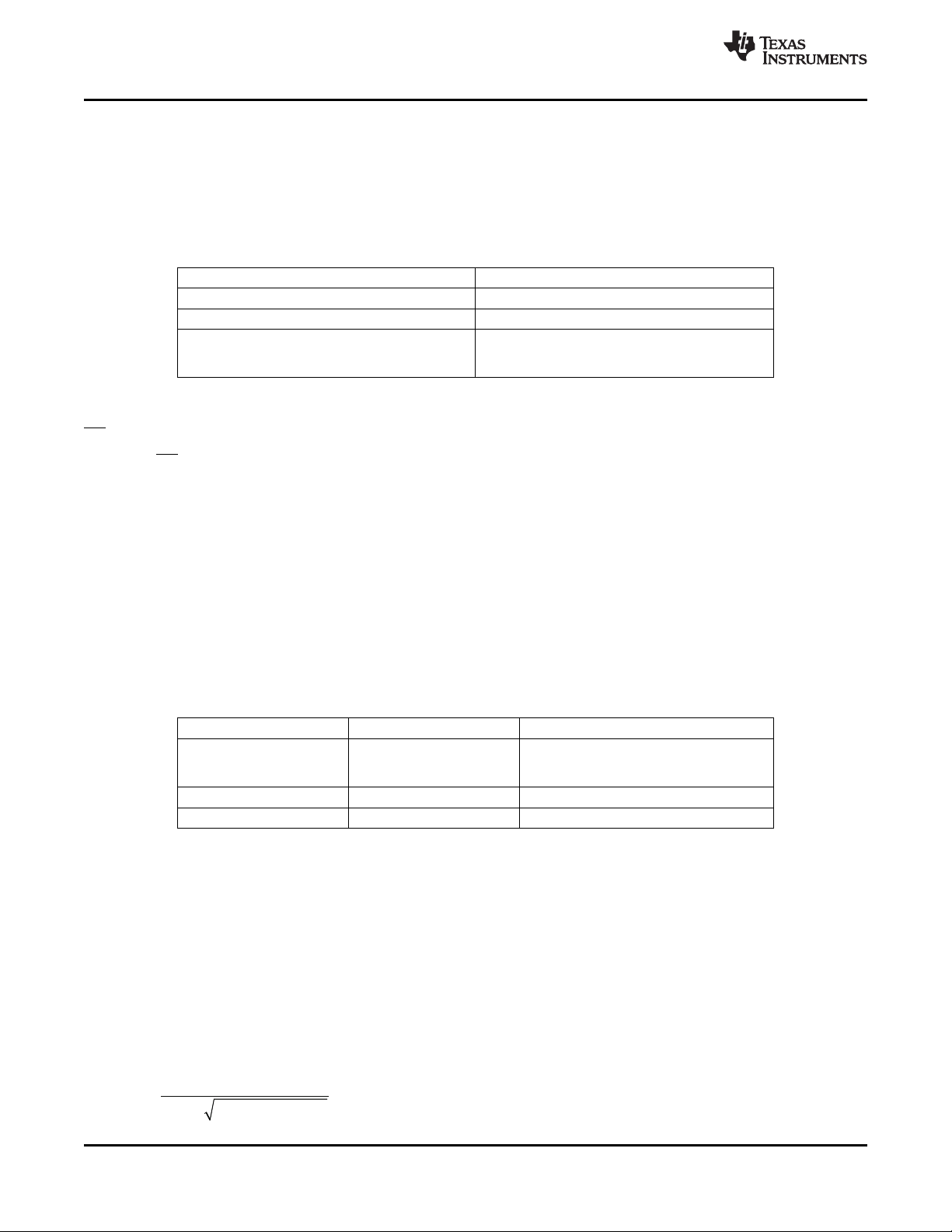
The bq24155 provides internal loop compensation. With this scheme, the best stability occurs when the LC
resonant frequency, ƒo, is approximately 40 kHz (20 kHz to 80 kHz). Equation 1 is used to calculate the value of
the output inductor, L
, and output capacitor, C
OUT
OUT
.
16 Submit Documentation Feedback Copyright © 2010, Texas Instruments Incorporated
(1)
Product Folder Link(s): bq24155
Page 17
STARTCondition
DATA
CLK
STOP Condition
S
P
bq24155
www.ti.com
SLUS942 –FEBRUARY 2010
To reduce the output voltage ripple, a ceramic capacitor with the capacitance between 4.7 mF and 47 mF is
recommended for C
, see the application section for components selection.
OUT
Pre-Regulator Application
Figure 2 shows a typical pre-regulator application that the bq24155 operates as a DC/DC converter, with the
termination disabled. In this application, the host charge controller controls switch Q to achieve pulse-charging
function, and bq24155 converts the input voltage to the lower output voltage (V
). The robust internal
OREG
compensation design ensures the stable operation when the host-controlled switch Q is turned off. With the input
overvoltage protection, output current regulation and high efficiency power conversion, the bq24155 is an ideal
choice for pre-regulator used in pulse charging applications.
SERIAL INTERFACE DESCRIPTION
I2C™ is a 2-wire serial interface developed by Philips Semiconductor (see I2C-Bus Specification, Version 2.1,
January 2000). The bus consists of a data line (SDA) and a clock line (SCL) with pull-up structures. When the
bus is idle, both SDA and SCL lines are pulled high. All the I2C compatible devices connect to the I2C bus
through open drain I/O pins, SDA and SCL. A master device, usually a microcontroller or a digital signal
processor, controls the bus. The master is responsible for generating the SCL signal and device addresses. The
master also generates specific conditions that indicate the START and STOP of data transfer. A slave device
receives and/or transmits data on the bus under control of the master device.
The bq24155 device works as a slave and is compatible with the following data transfer modes, as defined in the
I2C-Bus™ Specification: standard mode (100 kbps), fast mode (400 kbps), and high-speed mode (up to 3.4 Mbps
in write mode). The interface adds flexibility to the battery charge solution, enabling most functions to be
programmed to new values depending on the instantaneous application requirements. Register contents remain
intact as long as supply voltage remains above 2.2 V (typical). I2C is asynchronous, which means that it runs off
of SCL. The device has no noise or glitch filtering on SCL, so SCL input needs to be clean. Therefore, it is
recommended that SDA changes while SCL is LOW.
The data transfer protocol for standard and fast modes is exactly the same; therefore, they are referred to as the
F/S-mode in this document. The protocol for high-speed mode is different from the F/S-mode, and it is referred to
as the HS-mode. The bq24155 device only supports 7-bit addressing. The device 7-bit address is defined as
‘1101011’ (6BH).
F/S Mode Protocol
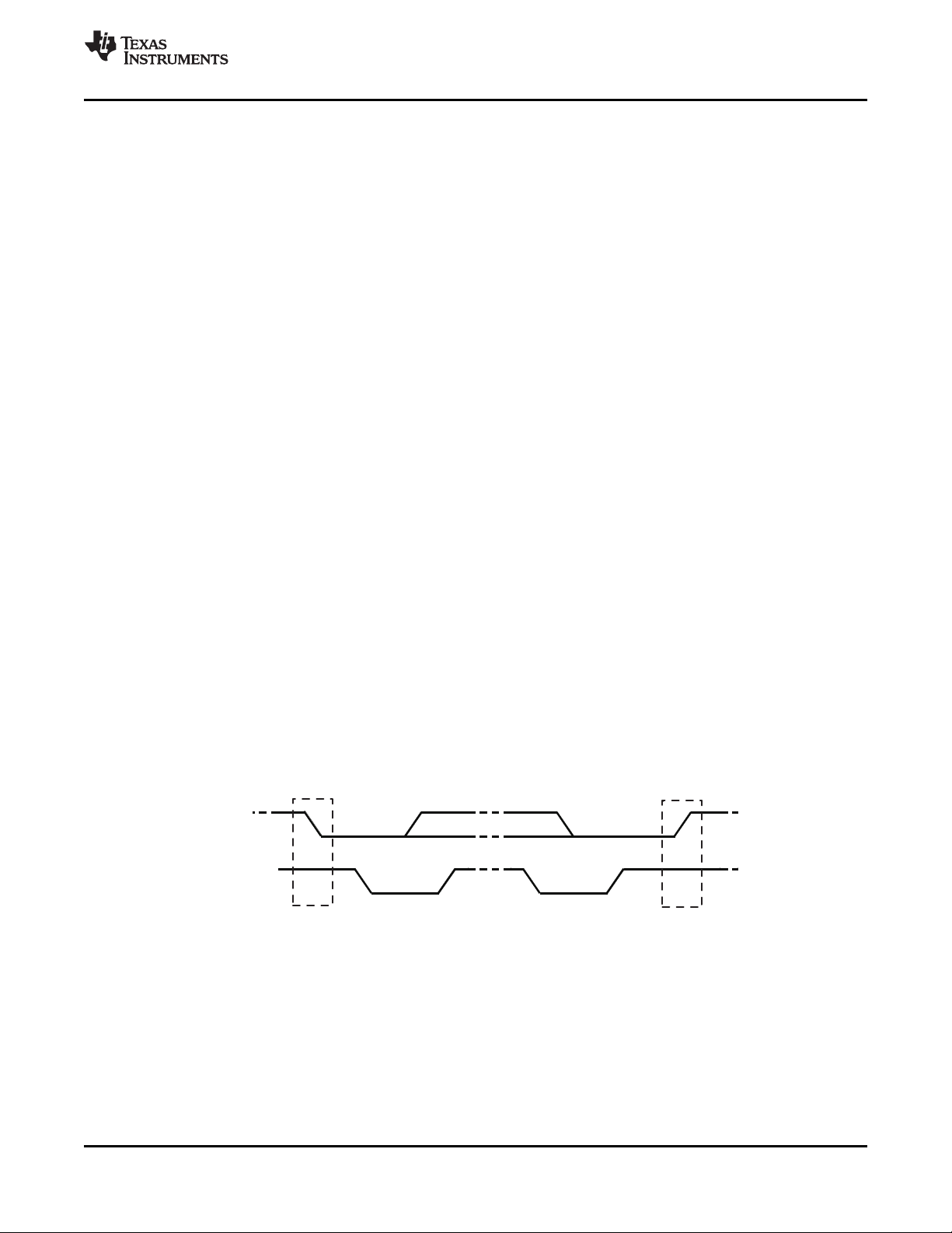
The master initiates data transfer by generating a start condition. The start condition is when a high-to-low
transition occurs on the SDA line while SCL is high, as shown in Figure 15. All I2C-compatible devices should
recognize a start condition.
Figure 15. START and STOP Condition
The master then generates the SCL pulses, and transmits the 8-bit address and the read/write direction bit R/W
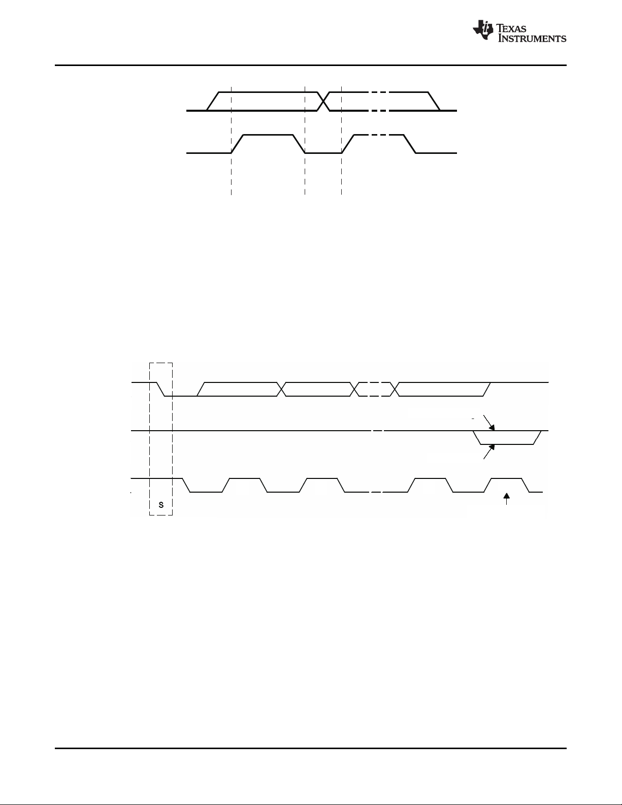
on the SDA line. During all transmissions, the master ensures that data is valid. A valid data condition requires
the SDA line to be stable during the entire high period of the clock pulse (see Figure 16). All devices recognize
the address sent by the master and compare it to their internal fixed addresses. Only the slave device with a
matching address generates an acknowledge (see Figure 16) by pulling the SDA line low during the entire high
period of the ninth SCL cycle. Upon detecting this acknowledge, the master knows that communication link with a
slave has been established.
Copyright © 2010, Texas Instruments Incorporated Submit Documentation Feedback 17
Product Folder Link(s): bq24155
Page 18
DATA
CLK
DataLine
Stable;
DataValid
Change
ofData
Allowed
DataOutput
byTransmitter
DataOutput
byReceiver
SCL From
Master
Not Acknowledge
Acknowledge
ClockPulsefor
Acknowledgement
1 2
8
9
START
Condition
bq24155
SLUS942 –FEBRUARY 2010
www.ti.com
Figure 16. Bit Transfer on the Serial Interface
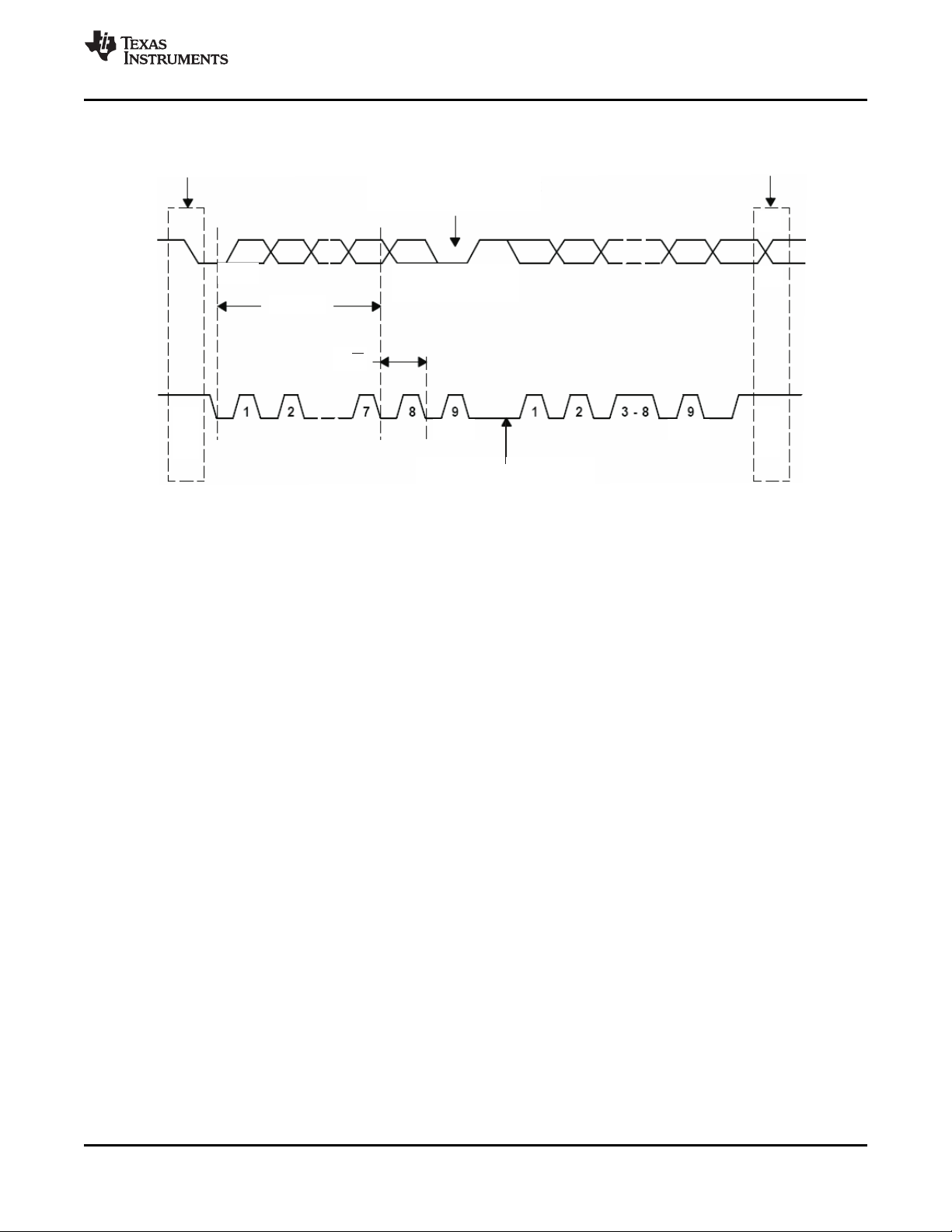
The master generates further SCL cycles to either transmit data to the slave (R/W bit 1) or receive data from the
slave (R/W bit 0). In either case, the receiver needs to acknowledge the data sent by the transmitter. So an
acknowledge signal can either be generated by the master or by the slave, depending on which one is the
receiver. the 9-bit valid data sequences consisting of 8-bit data and 1-bit acknowledge can continue as long as
necessary. To signal the end of the data transfer, the master generates a stop condition by pulling the SDA line
from low to high while the SCL line is high (see Figure 18). This releases the bus and stops the communication
link with the addressed slave. All I2C compatible devices must recognize the stop condition. Upon the receipt of a
stop condition, all devices know that the bus is released, and wait for a start condition followed by a matching
address. If a transaction is terminated prematurely, the master needs sending a STOP condition to prevent the
slave I2C logic from remaining in a bad state. Attempting to read data from register addresses not listed in this
section will result in FFh being read out.
Figure 17. Acknowledge on the I2C Bus™
18 Submit Documentation Feedback Copyright © 2010, Texas Instruments Incorporated
Product Folder Link(s): bq24155
Page 19
SDA
SCL
RecognizeSTARTor
REPRATEDSTART
Condition
RecognizeSTOP or
REPRATEDSTART
Condition
Generate ACKNOWLEDGE
Signal
Acknowledgement
SignalFromSlave
MSB
Address
R/W
ACK
ClockLineHeldLowWhile
InterruptsareServiced
S
or
Sr
Sr
or
P
P
Sr
ACK
bq24155
www.ti.com
SLUS942 –FEBRUARY 2010
Figure 18. Bus Protocol
H/S Mode Protocol
When the bus is idle, both SDA and SCL lines are pulled high by the pull-up devices.
The master generates a start condition followed by a valid serial byte containing HS master code '00001XXX'.
This transmission is made in F/S mode at no more than 400 Kbps. No device is allowed to acknowledge the HS
master code, but all devices must recognize it and switch their internal setting to support 3.4-Mbps operation
The master then generates a repeated start condition (a repeated start condition has the same timing as the start
condition). After this repeated start condition, the protocol is the same as F/S mode, except that transmission
speeds up to 3.4 Mbps are allowed. A stop condition ends the HS mode and switches all the internal settings of
the slave devices to support the F/S mode. Instead of using a stop condition, repeated start conditions should be
used to secure the bus in HS mode. If a transaction is terminated prematurely, the master needs sending a
STOP condition to prevent the slave I2C logic from remaining in a bad state.
Attempting to read data from register addresses not listed in this section results in FFh being read out.
bq24155 I2C Update Sequence
The bq24155 requires a start condition, a valid I2C address, a register address byte, and a data byte for a single
update. After the receipt of each byte, bq24155 device acknowledges by pulling the SDA line low during the high
period of a single clock pulse. A valid I2C address selects the bq24155. The bq24155 performs an update on the
falling edge of the acknowledge signal that follows the LSB byte.
For the first update, bq24155 requires a start condition, a valid I2C address, a register address byte, a data byte.
For all consecutive updates, bq24155 needs a register address byte, and a data byte. Once a stop condition is
received, the bq24155 releases the I2C bus, and awaits a new start conditions.
Copyright © 2010, Texas Instruments Incorporated Submit Documentation Feedback 19
Product Folder Link(s): bq24155
Page 20
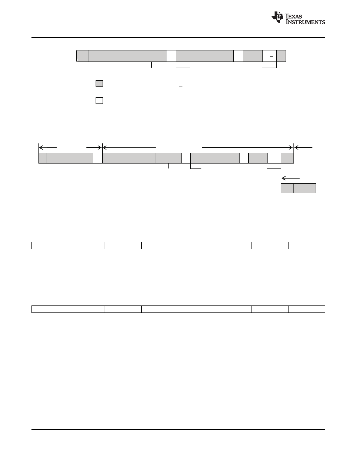
S SLAVE ADDRESS R/W A REGISTER ADDRESS A DATA
A/A
P
Data Transferred
‘0’ (Write) (n Bytes+ Acknowledge)
FrommastertotheIC A = Acknowledge(SDA LOW)
A = Notacknowledge(SDA
HIGH)
FromtheICtomaster S =STARTcondition
Sr =RepeatedSTARTcondition
P =STOP condition
(a) F/S-Mode
F/S-Mode HS-Mode
S HS-MASTERCODE
A
Sr SLAVE ADDRESS R/W A REGISTER ADDRESS A DATA
A/A
P
Data Transferred
‘0’ (write) (n Bytes+ Acknowledge)
Sr Slave A.
(b)HS- Mode
F/S-Mode
HS-Mode
Continues
bq24155
SLUS942 –FEBRUARY 2010
www.ti.com
Figure 19. Data Transfer Format in F/S Mode and H/S Mode
Slave Address Byte
MSB LSB
X 1 1 0 1 0 1 1
The slave address byte is the first byte received following the START condition from the master device. The
address bits are factory preset to ‘1101011’.
Register Address Byte
MSB LSB
0 0 0 0 0 D2 D1 D0
Following the successful acknowledgment of the slave address, the bus master will send a byte to the bq24155,
which contains the address of the register to be accessed. The bq24155 contains five 8-bit registers accessible
via a bidirectional I2C-bus interface. Among them, four internal registers have read and write access; and one
has only read access.
20 Submit Documentation Feedback Copyright © 2010, Texas Instruments Incorporated
Product Folder Link(s): bq24155
Page 21
bq24155
www.ti.com
SLUS942 –FEBRUARY 2010
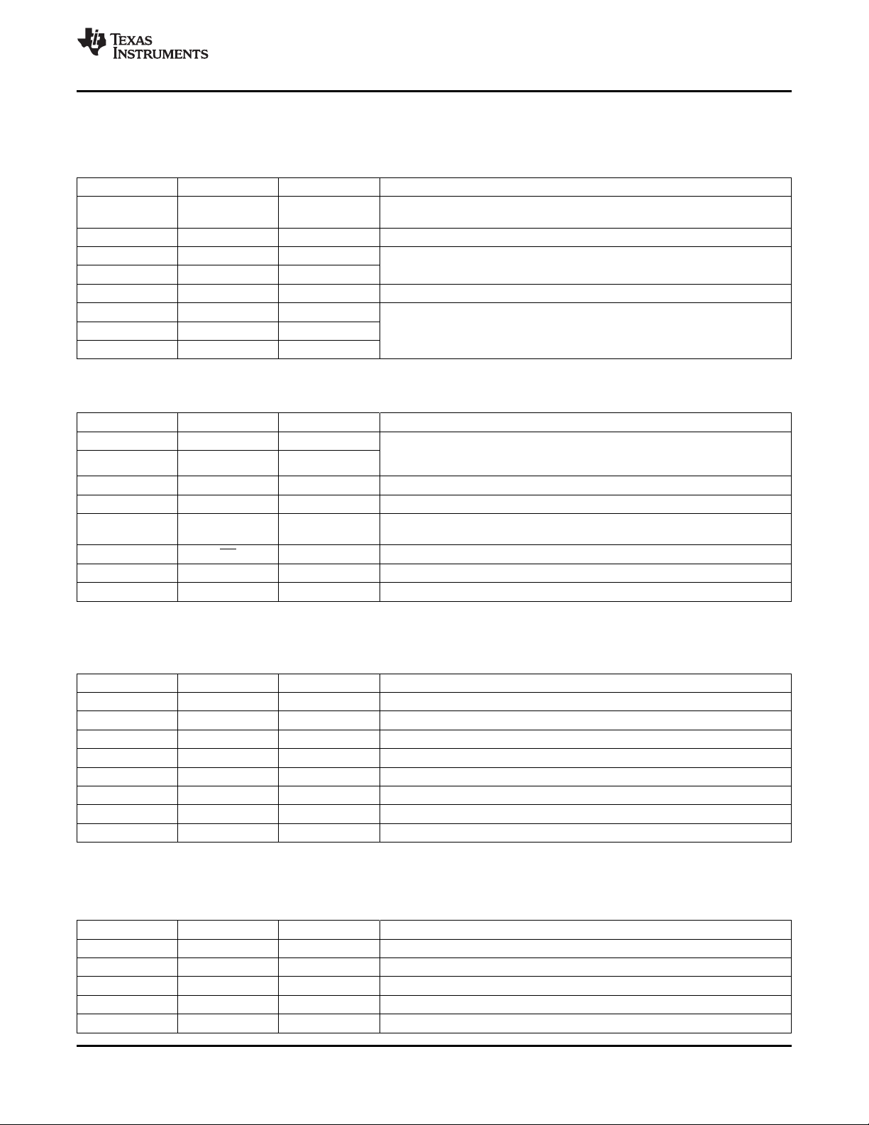
REGISTER DESCRIPTION
Table 3. Status/Control Register (Read/Write)
Memory Location: 00, Reset State: x1xx 0xxx
BIT NAME READ/WRITE FUNCTION
B7 (MSB) TMR_RST/ISEL Read/Write
B6 EN_STAT Read/Write 0-Disable STAT pin function, 1-Enable STAT pin function (default 1)
B5 STAT2 Read Only
B4 STAT1 Read Only
B3 BOOST Read Only NA
B2 FAULT_3 Read Only
B1 FAULT_2 Read Only source or VBUS < UVLO, 100-Output OVP, 101-Thermal shutdown, 110-Timer
B0 (LSB) FAULT_1 Read Only
Table 4. Control Register (Read/Write)
Memory Location: 01, Reset State: 0011 0000 (30H)
BIT NAME READ/WRITE FUNCTION
B7 (MSB) Iin_Limit_2 Read/Write 00-USB host with 100-mA current limit, 01-USB host with 500-mA current limit,
B6 Iin_Limit_1 Read/Write
B5 VLOWV_2
B4 VLOWV_1
B3 TE Read/Write
B2 CE Read/Write 1-Charger is disabled, 0-Charger enabled (default 0)
B1 HZ_MODE Read/Write 1-High impedance mode, 0-Not high impedance mode (default 0)
B0 (LSB) OPA_MODE Read/Write 1-NA, 0-Charger mode (default 0)
(1) The range of the weak battery voltage threshold (V
(1)
(1)
Read/Write 200-mV weak battery voltage threshold (default 1)
Read/Write 100-mV weak battery voltage threshold (default 1)
Write: TMR_RST function, write "1" to reset the safety timer (auto clear)
Read: ISEL pin status, 0-ISEL pin at Low level, 1-ISEL pin at High level
00-Ready, 01-Charge in progress, 10-Charge done, 11-Fault
Charge mode: 000-Normal, 001-VBUS OVP, 010-Sleep mode, 011-Poor input
fault, 111-No battery
10-USB host/charger with 800-mA current limit, 11-No input current limit
(default 00)
1-Enable charge current termination, 0-Disable charge current termination
(default 0)
) is 3.4 V to 3.7 V and step of 100 mV (default 3.7 V).
(LOWV)
Table 5. Control/Battery Voltage Register (Read/Write)
Memory Location: 02, Reset State: 0000 1010 (0AH)
BIT NAME READ/WRITE FUNCTION
B7 (MSB) V
B6 V
B5 V
B4 V
B3 V
B2 V
B1 NA Read/Write NA
B0 (LSB) NA Read/Write NA
O(REG5)
O(REG4)
O(REG3)
O(REG2)
O(REG1)
O(REG0)
Read/Write Battery regulation voltage: 640mV (default 0)
Read/Write Battery regulation voltage: 320mV (default 0)
Read/Write Battery regulation voltage: 160mV (default 0)
Read/Write Battery regulation voltage: 80mV (default 0)
Read/Write Battery regulation voltage: 40mV (default 1)
Read/Write Battery regulation voltage: 20mV (default 0)
Charge voltage range is 3.5 V to 4.44 V with the offset of 3.5 V and step of 20 mV (default is 3.54 V).
Table 6. Vender/Part/Revision Register (Read only)
Memory Location: 03, Reset State: 0100 x001
BIT NAME READ/WRITE FUNCTION
B7 (MSB) Vender2 Read Only Vender Code: bit 2 (default 0)
B6 Vender1 Read Only Vender Code: bit 1 (default 1)
B5 Vender0 Read Only Vender Code: bit 0 (default 0)
B4 PN1 Read Only Part Number Code: bit 1 (default 0)
B3 PN0 Read Only Part Number Code: bit 0 (default 0 for bq24151, default 1 for bq24155)
Copyright © 2010, Texas Instruments Incorporated Submit Documentation Feedback 21
Product Folder Link(s): bq24155
Page 22
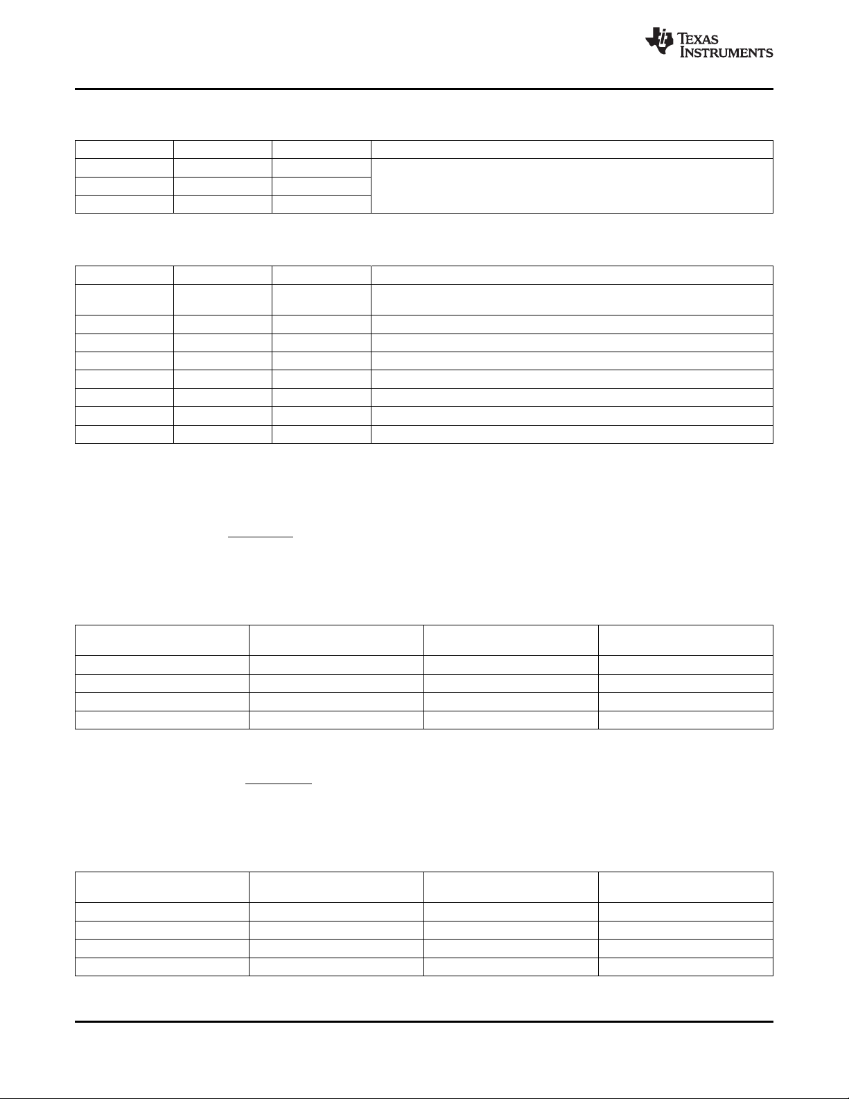
I(TERM0)
O(TERM_STEP)
(SNS)
V
I =
R
I(CHRG0)
O(CHARGE_STEP)
(SNS)
V
I =
R
bq24155
SLUS942 –FEBRUARY 2010
www.ti.com
Table 6. Vender/Part/Revision Register (Read only)
Memory Location: 03, Reset State: 0100 x001 (continued)
BIT NAME READ/WRITE FUNCTION
B2 Revision2 Read Only
B1 Revision1 Read Only
B0 (LSB) Revision0 Read Only
011: Revision 1.3;
100-111: Future Revisions
Table 7. Battery Termination/Fast Charge Current Register (Read/Write)
Memory Location: 04, Reset State: 1000 1001 (89H)
BIT NAME READ/WRITE FUNCTION
B7 (MSB) Reset Read/Write
B6 V
B5 V
B4 V
B3 NA Read/Write NA
B2 V
B1 V
B0 (LSB) V
I(CHRG2)
I(CHRG1)
I(CHRG0)
I(TERM2)
I(TERM1)
I(TERM0)
Read/Write Charge current sense voltage: 27.2mV (default 0)
Read/Write Charge current sense voltage: 13.6mV(default 0)
Read/Write Charge current sense voltage: 6.8mV (default 0)
Read/Write Termination current sense voltage: 13.6mV (default 0)
Read/Write Termination current sense voltage: 6.8mV (default 0)
Read/Write Termination current sense voltage: 3.4mV (default 1)
Write: 1-Charger in reset mode, 0-No effect
Read: always get "1"
Default charge current is 55 0mA and default termination current is 100 mA, if a 68-mΩ sensing resistor is used.
Both the termination current range and charge current range are depending on the sensing resistor R
termination current step (I
O(TERM_STEP)
) is calculated using Equation 2:
(SNS)
). The
Table 8 shows the termination current settings with two sensing resistors.
Table 8. Termination Current Settings for 68-mΩ and 100-mΩ Sense Resistors
I
(mA) I
BIT V
V
I(TERM2)
V
I(TERM1)
V
I(TERM0)
Offset 3.4 50 34
The charge current step (I
O(CHARGE_STEP)
(mV)
I(TERM)
13.6 200 136
6.8 100 68
3.4 50 34
) is calculated using Equation 3:
(TERM)
R
= 68mΩ R
(SNS)
Table 9 shows the charge current settings with two sensing resistors.
Table 9. Charge Current Settings for 68-mΩ and 100-mΩ Sense Resistors
I
BIT V
V
I(CHRG2)
V
I(CHRG1)
V
I(CHRG0)
Offset 37.4 550 374
(mV)
I(REG)
27.2 400 272
13.6 200 136
6.8 100 68
O(CHARGE)
R
= 68mΩ R
(SNS)
(mA) I
(TERM)
= 100mΩ
(SNS)
O(CHARGE)
= 100mΩ
(SNS)
(2)
(mA)
(3)
(mA)
22 Submit Documentation Feedback Copyright © 2010, Texas Instruments Incorporated
Product Folder Link(s): bq24155
Page 23
V
IN
+
-
C1
C2
PMID
VBUS
SW
L1
PGND
bq2415xA
C4
Isns
Rsns
C3
Ichg
BAT
+
Isys
System
Load
bq24155
www.ti.com
SLUS942 –FEBRUARY 2010
POWER TOPOLOGIES
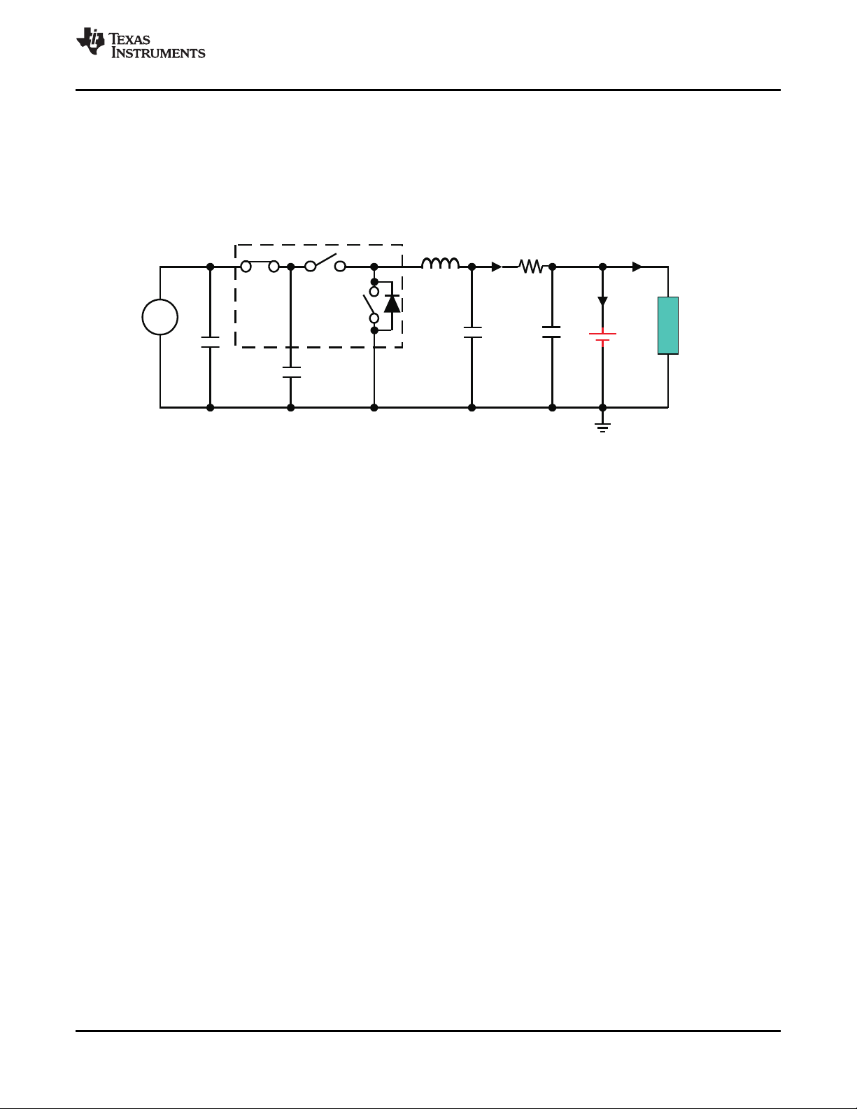
System Load After Sensing Resistor
One of the simple high-efficiency topologies connects the system load directly across the battery pack, as shown
in Figure 20. The input voltage has been converted to a usable system voltage with good efficiency from the
input. When the input power is on, it supplies the system load and charges the battery pack at the same time.
When the input power is off, the battery pack powers the system directly.
Figure 20. System Load After Sensing Resistor
The advantages:
• When the AC adapter is disconnected, the battery pack powers the system load with minimum power
dissipations. Consequently, the time that the system runs on the battery pack can be maximized.
• It saves the external path selection components and offers a low-cost solution.
• Dynamic power management (DPM) can be achieved. The total of the charge current and the system current
can be limited to a desired value by adjusting charge current. When the system current increases, the charge
current drops by the same amount. As a result, no potential over-current or over-heating issues are caused
by excessive system load demand.
• The total of the input current can be limited to a desired value by setting input current limit value. So USB
specifications can be met easily.
• The supply voltage variation range for the system can be minimized.
• The input current soft-start can be achieved by the generic soft-start feature of the IC.
Design considerations and potential issues:
• If the system always demands a high current (but lower than the regulation current), the charging never
terminates. Thus, the battery is always charged, and the lifetime may be reduced.
• Because the total current regulation threshold is fixed and the system always demands some current, the
battery may not be charged with a full-charge rate and thus may lead to a longer charge time.
• If the system load current is large after the charger has been terminated, the voltage drop across the battery
impedance may cause the battery voltage to drop below the refresh threshold and start a new charge. The
charger would then terminate due to low charge current. Therefore, the charger would cycle between
charging and terminating. If the load is smaller, the battery has to discharge down to the refresh threshold,
resulting in a much slower cycling.
• In a charger system, the charge current is typically limited to about 10mA, if the sensed battery voltage is
below 2V short circuit protection threshold. This results in low power availability at the system bus. If an
external supply is connected and the battery is deeply discharged, below the short circuit protection threshold,
the charge current is clamped to the short circuit current limit. This then is the current available to the system
during the power-up phase. Most systems cannot function with such limited supply current, and the battery
supplements the additional power required by the system. Note that the battery pack is already at the
depleted condition, and it discharges further until the battery protector opens, resulting in a system shutdown.
• If the battery is below the short circuit threshold and the system requires a bias current budget lower than the
short circuit current limit, the end-equipment will be operational, but the charging process can be affected
depending on the current left to charge the battery pack. Under extreme conditions, the system current is
Copyright © 2010, Texas Instruments Incorporated Submit Documentation Feedback 23
Product Folder Link(s): bq24155
Page 24
V
IN
+
-
C1
C2
PMID
VBUS
SW
L1
PGND
bq2415xA
C4
Isns
Rsns
C3
Ichg
BAT
+
Isys
System
Load
bq24155
SLUS942 –FEBRUARY 2010
www.ti.com
close to the short circuit current levels and the battery may not reach the fast-charge region in a timely
manner. As a result, the safety timers flag the battery pack as defective, terminating the charging process.
Because the safety timer cannot be disabled, the inserted battery pack must not be depleted to make the
application possible.
• For instance, if the battery pack voltage is too low, highly depleted, or totally dead or even shorted, the
system voltage is clamped by the battery and it cannot operate even if the input power is on.
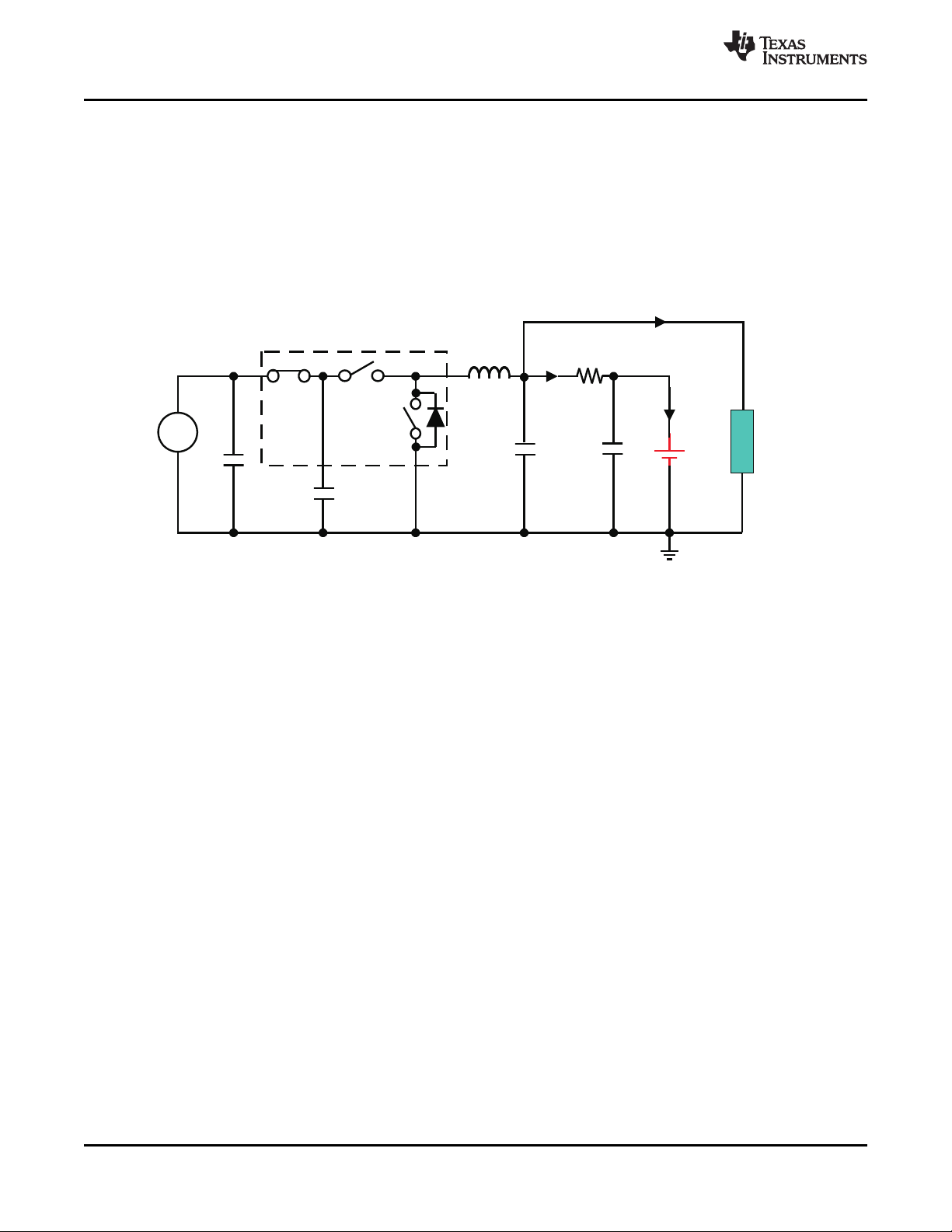
System Load Before Sensing Resistor
The second circuit is very similar to first one; the difference is that the system load is connected before the sense
resistor, as shown in Figure 21.
Figure 21. System Load Before Sensing Resistor
The advantages of system load before sensing resistor to system load after sensing resistor:
• The charger controller is based only on the current goes through the current-sense resistor. So, the constant
current fast charge and termination functions work well, and are not affected by the system load. This is the
major advantage of it.
• A depleted battery pack can be connected to the charger without the risk of the safety timer expiration caused
by high system load.
• The charger can disable termination and keep the converter running to keep battery fully charged, or let the
switcher terminate when the battery is full and then run off of the battery via the sense resistor.
Design considerations and potential issues:
• The total current is limited by the IC input current limit, or peak current protection but not the charge current
setting. The charge current does not drop when the system current load increases until the input current limit
is reached. This solution is not applicable if the system requires a high current.
• Efficiency declines when discharging through the sense resistor to the system.
• No thermal regulation. Therefore, system design should ensure the maximum junction temperature of the IC
is below 125°C during normal operation.
DESIGN EXAMPLE FOR TYPICAL APPLICATION CIRCUITS
Systems Design Specifications:
• VBUS = 5 V
• V
• I
• Inductor ripple current = 30% of fast charge current
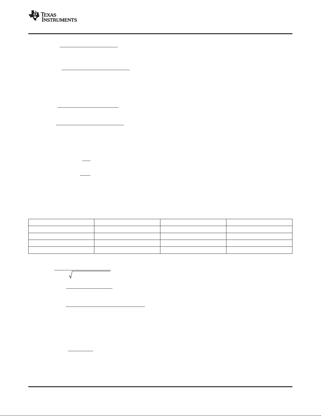
1. Determine the inductor value (L
= 4.2 V (1-Cell)
(BAT)
= 1.25 A
(charge)
OUT
) for the specified charge current ripple:
24 Submit Documentation Feedback Copyright © 2010, Texas Instruments Incorporated
Product Folder Link(s): bq24155
Page 25
´
´ ´ D
OU T
L
VB AT (VB US - VBA T)
L =
VB US If
OUT
6
2.5 (5 - 2.5)
L =
5 (3 10 ) 1.25 0.3
´
´ ´ ´ ´
´
D
´ ´
L
OUT
VBAT (VBUS - VBAT)
I =
VBUS Lf
L
-6
2.5 (5 - 2.5)
I =
6
5 (3 10 ) (1 10 )
´
D
´ ´ ´ ´
L
LPK OUT
I
I I
2
D
= +
LP K
0.42
I 1 .2 5
2
= +
OUT OUT
1
=
o
2 L C
f
p ´ ´
2 2
OUT
OUT
1
C
4 L
0
f
=
p ´ ´
2 3 2 -6
OUT
1
C
4 (40 10 ) (1 10 )
=
p ´ ´ ´ ´
(RSNS)
(SNS)
(CHARGE)
V
R
I
=
bq24155
www.ti.com
SLUS942 –FEBRUARY 2010
, the worst case is when battery voltage is as close as to half of the input
voltage.
L
= 1.11 mH
OUT
Select the output inductor to standard 1 mH. Calculate the total ripple current with using the 1 mH inductor:
ΔIL= 0.42 A
Calculate the maximum output current:
I
= 1.46 A
LPK
Select 2.5mm by 2.0mm 1-mH 1.5-A surface mount multi-layer inductor. The suggested inductor part
numbers are shown as following.
(4)
(5)
(6)
(7)
(8)
Table 10. Inductor Part Numbers
PART NUMBER INDUCTANCE SIZE MANUFACTURER
LQM2HPN1R0MJ0 1 mH 2.5 x 2.0 mm muRata
MIPS2520D1R0 1 mH 2.5 x 2.0 mm FDK
MDT2520-CN1R0M 1 mH 2.5 x 2.0 mm TOKO
CP1008 1 mH 2.5 x 2.0 mm Inter-Technical
2. Determine the output capacitor value C
C
= 15.8 mF
OUT
using 40 kHz as the resonant frequency:
OUT
Select two 0603 X5R 6.3V 10-mF ceramic capacitors in parallel i.e., muRata GRM188R60J106M.
3. Determine the sense resistor using the following equation:
The maximum sense voltage across sense resistor is 85 mV. In order to get a better current regulation
accuracy, V
should equal 85 mV, and calculate the value for the sense resistor.
(RSNS)
(9)
(10)
(11)
(12)
Copyright © 2010, Texas Instruments Incorporated Submit Documentation Feedback 25
Product Folder Link(s): bq24155
Page 26
(SNS)
85mV
R
1.25A
=
BatteryChargeEfficiency
82
83
84
85
86
87
88
89
90
500 600 700 800 900 1000 1100 1200 1300
ChargeCurrent-mA
Efficiency-%
TOKO
FDK
muRata
Inter-Technical
BatteryChargeLoss
100
200
300
400
500
600
700
800
500 600 700 800 900 1000 1100 1200 1300
Loss-mW
ChargeCurrent-mA
T =25°C,
VBUS=5V,
VBAT=3V
A
T =25°C,
VBUS=5V,
VBAT=3V
A
TOKO
FDK
muRata
Inter-Technical
bq24155
SLUS942 –FEBRUARY 2010
R
= 68 mΩ
(SNS)
This is a standard value. If it is not a standard value, then choose the next close value and calculate the real
charge current. Calculate the power dissipation on the sense resistor:
P
(RSNS)
P
(RSNS)
P
(RSNS)
= I
(CHARGE)
= 1252× 0.068
= 0.106 W
2
× R
(SNS)
Select 0402 0.125-W 68-mΩ 2% sense resistor, i.e. Panasonic ERJ2BWGR068.
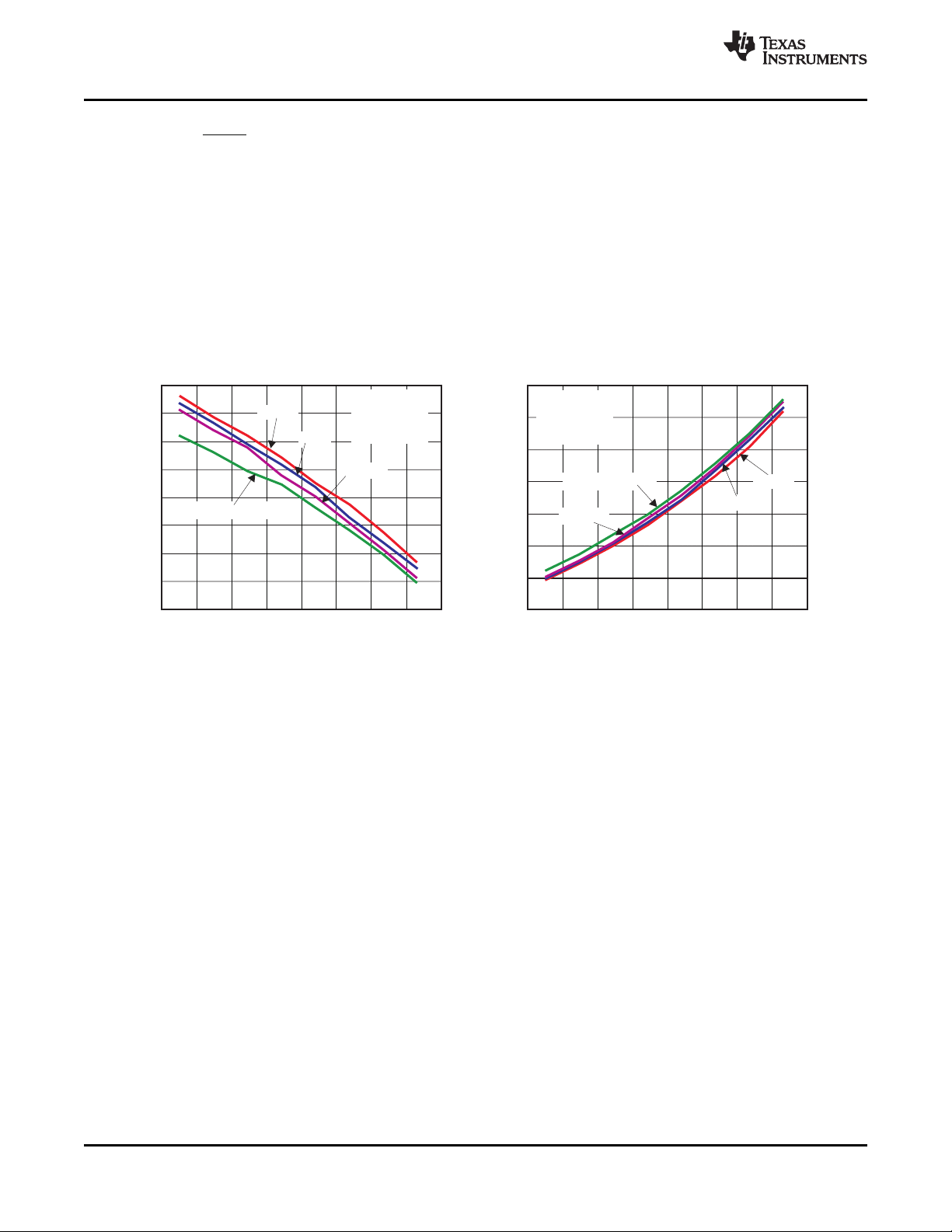
4. Measured efficiency and total power loss for different inductors are shown in Figure 22.
www.ti.com
(13)
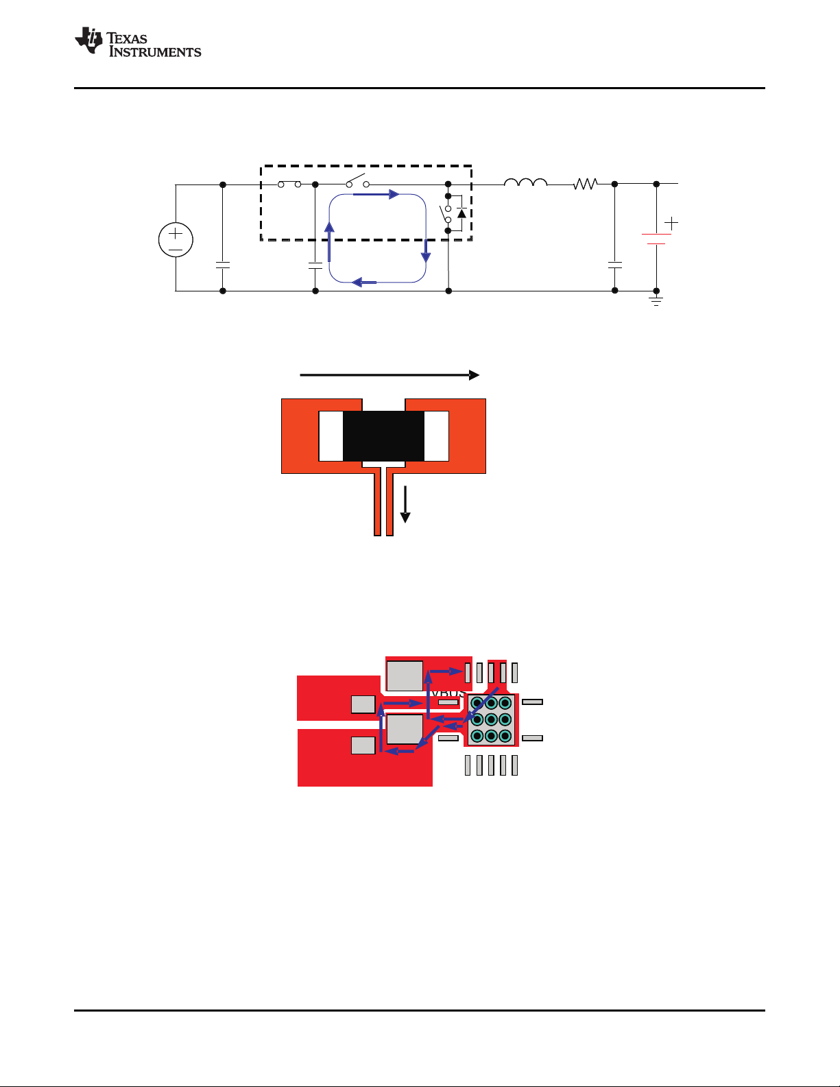
It is important to pay special attention to the PCB layout. The following provides some guidelines:
• To obtain optimal performance, the power input capacitors, connected from input to PGND, should be placed
as close as possible to the bq24155. The output inductor should be placed close to the IC and the output
capacitor connected between the inductor and PGND of the IC. The intent is to minimize the current path loop
area from the SW pin through the LC filter and back to the PGND pin. To prevent high frequency oscillation
problems, proper layout to minimize high frequency current path loop is critical (see Figure 23). The sense
resistor should be adjacent to the junction of the inductor and output capacitor. Route the sense leads
connected across the RSNS back to the IC, close to each other (minimize loop area) or on top of each other
on adjacent layers (do not route the sense leads through a high-current path, see Figure 24).
• Place all decoupling capacitor close to their respective IC pin and as close as to PGND (do not place
components such that routing interrupts power stage currents). All small control signals should be routed
away from the high current paths.
• The PCB should have a ground plane (return) connected directly to the return of all components through vias
(two vias per capacitor for power-stage capacitors, two vias for the IC PGND, one via per capacitor for
small-signal components). A star ground design approach is typically used to keep circuit block currents
isolated (high-power/low-power small-signal) which reduces noise-coupling and ground-bounce issues. A
single ground plane for this design gives good results. With this small layout and a single ground plane, there
is no ground-bounce issue, and having the components segregated minimizes coupling between signals.
• The high-current charge paths into VBUS, PMID and from the SW pins must be sized appropriately for the
maximum charge current in order to avoid voltage drops in these traces. The PGND pins should be
connected to the ground plane to return current through the internal low-side FET.
26 Submit Documentation Feedback Copyright © 2010, Texas Instruments Incorporated
Figure 22. Measured Efficiency and Power Loss
PCB LAYOUT CONSIDERATION
Product Folder Link(s): bq24155
Page 27
High
Frequency
Current
Path
L1
R1
C3
C1
VBUS
PMID
C2
PGND
SW
V
BAT
BAT
V
IN
ChargeCurrentDirection
ToCSINandCSOUTpin
R
SNS
ToInductor ToCapacitorandbattery
CurrentSensingDirection
PMID
SW
PGND
4.7uF
1uF
Vin+
Vin-
AGND
VBUS
PMID
SW
PGND
4.7uF
1uF
Vin+
Vin-
AGND
VBUS
bq24155
www.ti.com
SLUS942 –FEBRUARY 2010
• Place 4.7uF input capacitor as close to PMID pin and PGND pin as possible to make high frequency current
loop area as small as possible. Place 1uF input capacitor as close to VBUS pin and PGND pin as possible to
make high frequency current loop area as small as possible (see Figure 25).
Figure 23. High Frequency Current Path
Figure 24. Sensing Resistor PCB Layout
Figure 25. Input Capacitor Position and PCB Layout Example
Copyright © 2010, Texas Instruments Incorporated Submit Documentation Feedback 27
Product Folder Link(s): bq24155
Page 28

PACKAGE OPTION ADDENDUM
www.ti.com 17-Mar-2010
PACKAGING INFORMATION
Orderable Device Status
(1)
Package
Type
Package
Drawing
Pins Package
Qty
Eco Plan
BQ24155RGYR ACTIVE VQFN RGY 14 3000 Green (RoHS &
(2)
Lead/Ball Finish MSL Peak Temp
CU NIPDAU Level-2-260C-1 YEAR
(3)
no Sb/Br)
BQ24155RGYT ACTIVE VQFN RGY 14 250 Green (RoHS &
CU NIPDAU Level-2-260C-1 YEAR
no Sb/Br)
(1)
The marketing status values are defined as follows:
ACTIVE: Product device recommended for new designs.
LIFEBUY: TI has announced that the device will be discontinued, and a lifetime-buy period is in effect.
NRND: Not recommended for new designs. Device is in production to support existing customers, but TI does not recommend using this part in
a new design.
PREVIEW: Device has been announced but is not in production. Samples may or may not be available.
OBSOLETE: TI has discontinued the production of the device.
(2)
Eco Plan - The planned eco-friendly classification: Pb-Free (RoHS), Pb-Free (RoHS Exempt), or Green (RoHS & no Sb/Br) - please check
http://www.ti.com/productcontent for the latest availability information and additional product content details.
TBD: The Pb-Free/Green conversion plan has not been defined.
Pb-Free (RoHS): TI's terms "Lead-Free" or "Pb-Free" mean semiconductor products that are compatible with the current RoHS requirements
for all 6 substances, including the requirement that lead not exceed 0.1% by weight in homogeneous materials. Where designed to be soldered
at high temperatures, TI Pb-Free products are suitable for use in specified lead-free processes.
Pb-Free (RoHS Exempt): This component has a RoHS exemption for either 1) lead-based flip-chip solder bumps used between the die and
package, or 2) lead-based die adhesive used between the die and leadframe. The component is otherwise considered Pb-Free (RoHS
compatible) as defined above.
Green (RoHS & no Sb/Br): TI defines "Green" to mean Pb-Free (RoHS compatible), and free of Bromine (Br) and Antimony (Sb) based flame
retardants (Br or Sb do not exceed 0.1% by weight in homogeneous material)
(3)
MSL, Peak Temp. -- The Moisture Sensitivity Level rating according to the JEDEC industry standard classifications, and peak solder
temperature.
Important Information and Disclaimer:The information provided on this page represents TI's knowledge and belief as of the date that it is
provided. TI bases its knowledge and belief on information provided by third parties, and makes no representation or warranty as to the
accuracy of such information. Efforts are underway to better integrate information from third parties. TI has taken and continues to take
reasonable steps to provide representative and accurate information but may not have conducted destructive testing or chemical analysis on
incoming materials and chemicals. TI and TI suppliers consider certain information to be proprietary, and thus CAS numbers and other limited
information may not be available for release.
In no event shall TI's liability arising out of such information exceed the total purchase price of the TI part(s) at issue in this document sold by TI
to Customer on an annual basis.
Addendum-Page 1
Page 29
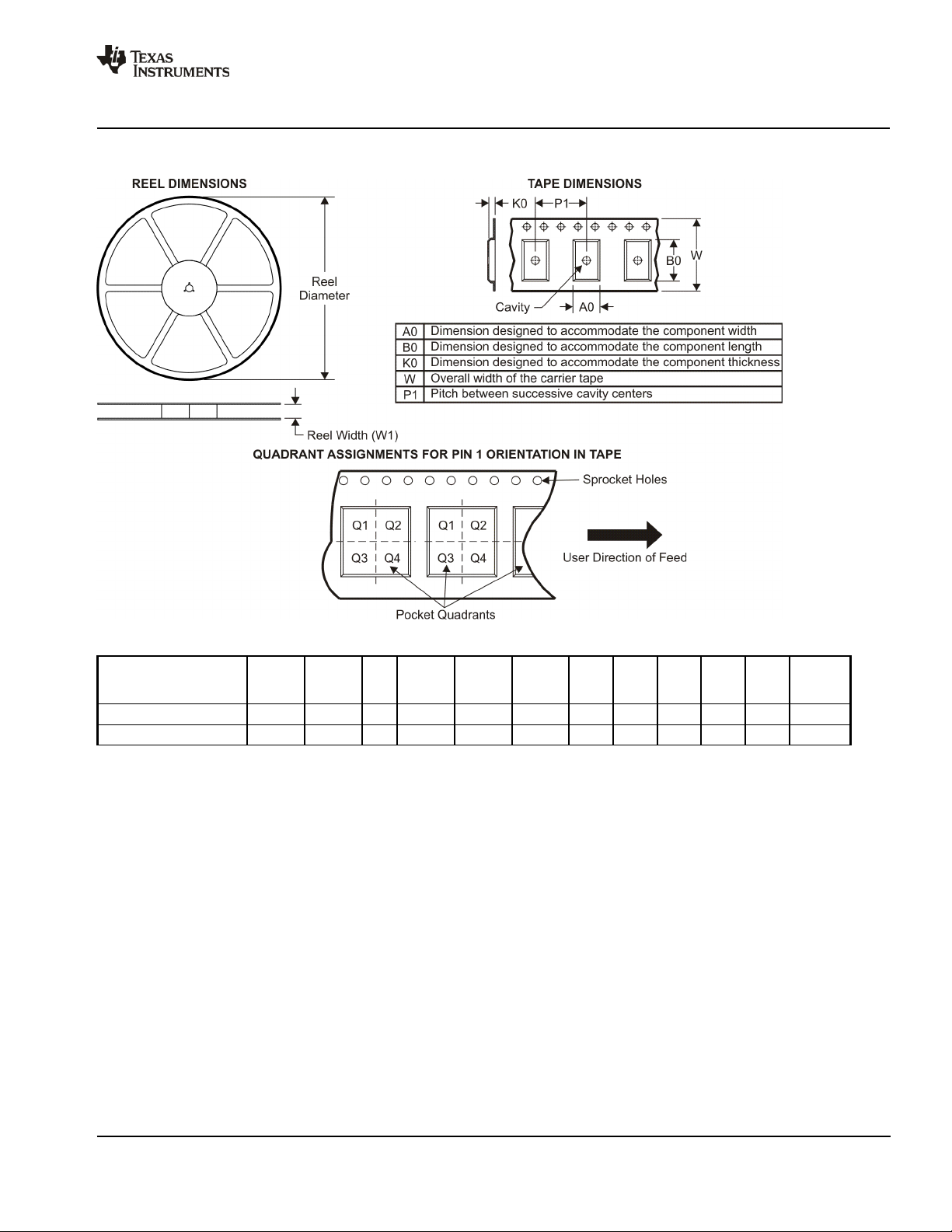
PACKAGE MATERIALS INFORMATION
www.ti.com 20-Jul-2010
TAPE AND REEL INFORMATION
*All dimensions are nominal
Device Package
BQ24155RGYR VQFN RGY 14 3000 330.0 12.4 3.75 3.75 1.15 8.0 12.0 Q1
BQ24155RGYT VQFN RGY 14 250 180.0 12.4 3.75 3.75 1.15 8.0 12.0 Q1
Type
Package
Drawing
Pins SPQ Reel
Diameter
(mm)
Reel
Width
W1 (mm)
A0
(mm)B0(mm)K0(mm)P1(mm)W(mm)
Pin1
Quadrant
Pack Materials-Page 1
Page 30
PACKAGE MATERIALS INFORMATION
www.ti.com 20-Jul-2010
*All dimensions are nominal
Device Package Type Package Drawing Pins SPQ Length (mm) Width (mm) Height (mm)
BQ24155RGYR VQFN RGY 14 3000 346.0 346.0 29.0
BQ24155RGYT VQFN RGY 14 250 190.5 212.7 31.8
Pack Materials-Page 2
Page 31
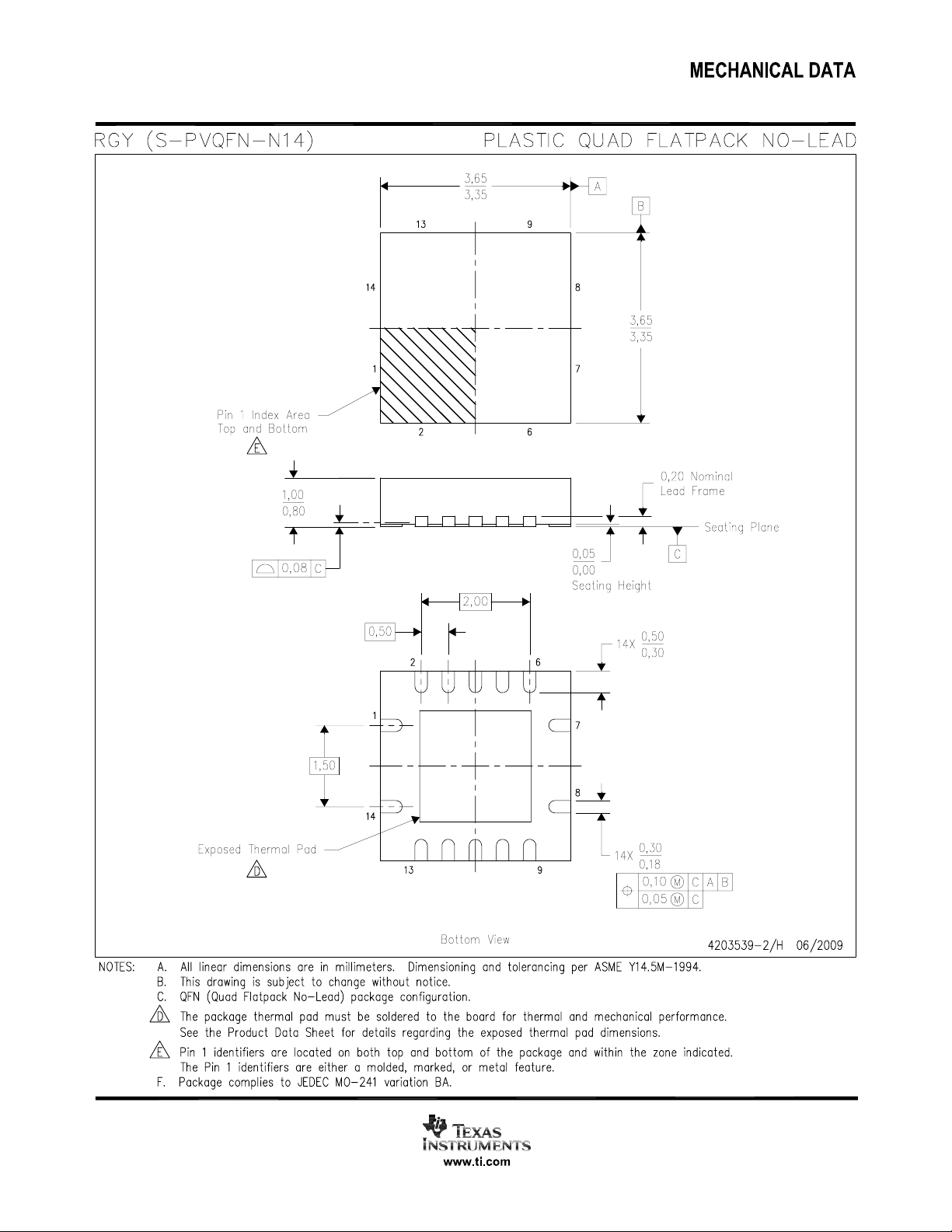
Page 32
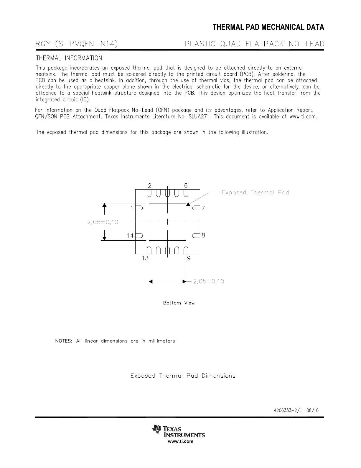
Page 33
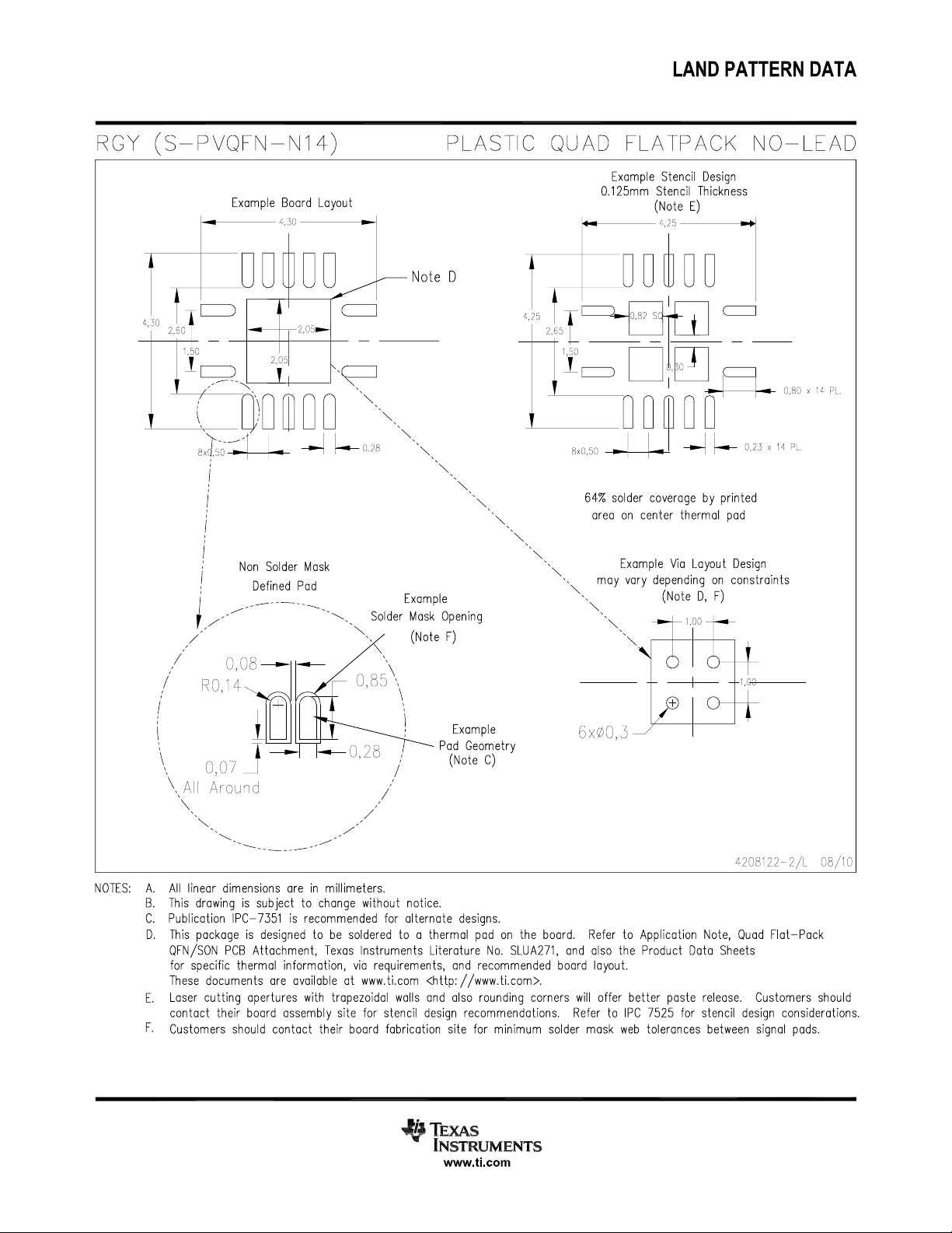
Page 34

IMPORTANT NOTICE
Texas Instruments Incorporated and its subsidiaries (TI) reserve the right to make corrections, modifications, enhancements, improvements,
and other changes to its products and services at any time and to discontinue any product or service without notice. Customers should
obtain the latest relevant information before placing orders and should verify that such information is current and complete. All products are
sold subject to TI’s terms and conditions of sale supplied at the time of order acknowledgment.
TI warrants performance of its hardware products to the specifications applicable at the time of sale in accordance with TI’s standard
warranty. Testing and other quality control techniques are used to the extent TI deems necessary to support this warranty. Except where
mandated by government requirements, testing of all parameters of each product is not necessarily performed.
TI assumes no liability for applications assistance or customer product design. Customers are responsible for their products and
applications using TI components. To minimize the risks associated with customer products and applications, customers should provide
adequate design and operating safeguards.
TI does not warrant or represent that any license, either express or implied, is granted under any TI patent right, copyright, mask work right,
or other TI intellectual property right relating to any combination, machine, or process in which TI products or services are used. Information
published by TI regarding third-party products or services does not constitute a license from TI to use such products or services or a
warranty or endorsement thereof. Use of such information may require a license from a third party under the patents or other intellectual
property of the third party, or a license from TI under the patents or other intellectual property of TI.
Reproduction of TI information in TI data books or data sheets is permissible only if reproduction is without alteration and is accompanied
by all associated warranties, conditions, limitations, and notices. Reproduction of this information with alteration is an unfair and deceptive
business practice. TI is not responsible or liable for such altered documentation. Information of third parties may be subject to additional
restrictions.
Resale of TI products or services with statements different from or beyond the parameters stated by TI for that product or service voids all
express and any implied warranties for the associated TI product or service and is an unfair and deceptive business practice. TI is not
responsible or liable for any such statements.
TI products are not authorized for use in safety-critical applications (such as life support) where a failure of the TI product would reasonably
be expected to cause severe personal injury or death, unless officers of the parties have executed an agreement specifically governing
such use. Buyers represent that they have all necessary expertise in the safety and regulatory ramifications of their applications, and
acknowledge and agree that they are solely responsible for all legal, regulatory and safety-related requirements concerning their products
and any use of TI products in such safety-critical applications, notwithstanding any applications-related information or support that may be
provided by TI. Further, Buyers must fully indemnify TI and its representatives against any damages arising out of the use of TI products in
such safety-critical applications.
TI products are neither designed nor intended for use in military/aerospace applications or environments unless the TI products are
specifically designated by TI as military-grade or "enhanced plastic." Only products designated by TI as military-grade meet military
specifications. Buyers acknowledge and agree that any such use of TI products which TI has not designated as military-grade is solely at
the Buyer's risk, and that they are solely responsible for compliance with all legal and regulatory requirements in connection with such use.
TI products are neither designed nor intended for use in automotive applications or environments unless the specific TI products are
designated by TI as compliant with ISO/TS 16949 requirements. Buyers acknowledge and agree that, if they use any non-designated
products in automotive applications, TI will not be responsible for any failure to meet such requirements.
Following are URLs where you can obtain information on other Texas Instruments products and application solutions:
Products Applications
Amplifiers amplifier.ti.com Audio www.ti.com/audio
Data Converters dataconverter.ti.com Automotive www.ti.com/automotive
DLP® Products www.dlp.com Communications and www.ti.com/communications
DSP dsp.ti.com Computers and www.ti.com/computers
Clocks and Timers www.ti.com/clocks Consumer Electronics www.ti.com/consumer-apps
Interface interface.ti.com Energy www.ti.com/energy
Logic logic.ti.com Industrial www.ti.com/industrial
Power Mgmt power.ti.com Medical www.ti.com/medical
Microcontrollers microcontroller.ti.com Security www.ti.com/security
RFID www.ti-rfid.com Space, Avionics & www.ti.com/space-avionics-defense
RF/IF and ZigBee® Solutions www.ti.com/lprf Video and Imaging www.ti.com/video
Mailing Address: Texas Instruments, Post Office Box 655303, Dallas, Texas 75265
Copyright © 2010, Texas Instruments Incorporated
Telecom
Peripherals
Defense
Wireless www.ti.com/wireless-apps
 Loading...