

bq24728 DATASHEET
1-4 Cell Li+ Battery SMBus Charge Controller with N-Channel Power
MOSFET Selector and Advanced Circuit Protection
JUN 21, 2011
FEATURES
• Programmable Adapter Detection and
Indicator Support Air Mode Adapter
• SMBus Host-Controlled NMOS-NMOS
Synchronous Buck Converter with
Programmable 615kHz, 750kHz, and 885kHz
Switching Frequencies
• Automatic N-channel MOSFET Selection of
System Power Source from Adapter or Battery
Driven by Internal Charge Pumps
• Enhanced Safety Features for Over Voltage
Protection, Over Current Protection, Battery,
Inductor and MOSFET Short Circuit Protection
• Programmable Input Current, Charge Voltage,
Charge Current Limits
o +/-0.5% Charge Voltage Accuracy up to 19.2V
o +/-3% Charge Current Accuracy up to 8.128A
o +/-3% Input Current Accuracy up to 8.064A
o +/-2% 20x Adapter Current or Charge Current
Amplifier Output Accuracy
• Programmable Battery Depletion Threshold,
and Battery LEARN Function
• Integrated Soft Start
• Integrated Loop Compensation
• Real Time System Control on ILIM pin to Limit
Charge Current
• AC Adapter Operating Range 4.5V-24V
• 5uA Off-State Battery Discharge Curr ent
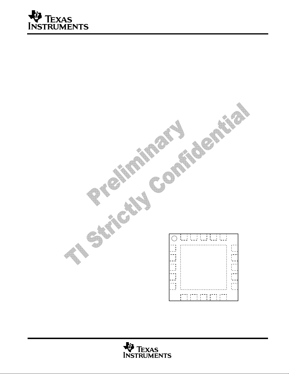
• 20-pin 3.5x3.5 mm
APPLICATIONS
2
QFN Package
• Portable Notebook Computers, UMPC, Ultra-
Thin Notebook, and Netbook
• Handheld Terminal
• Industrial and Medical Equipment
• Portable Equipment
DESCRIPTION
The bq24728 is a high-efficiency, synchronous battery
charger, offering low component count for spaceconstraint, multi-chemistry battery charging
applications.
The bq24728 utilizes two charge pumps to separately
drive n-channel MOSFETs (ACFET, RBFET and
BATFET) for automatic system power source
selection. Its programmable adapter detection and
indicator supports air mode adapter and AC adapter.
SMBus controlled input current, charge current, and
charge voltage DACs allow for very high regulation
accuracies that can be easily programmed by the
system power management micro-controller.
The bq24728 uses internal input current register or
external ILIM pin to throttle down PWM modulation to
reduce the charge current.
The bq24728 charges one, two, three or four series
Li+ cells, and is available in a 20-pin, 3.5x3.5 mm
2
QFN package.
PIN CONFIGURATION
ACN
ACN
ACP
ACP
CMSRC
CMSRC
ACDRV
ACDRV
ACPRES
ACPRES
VCC
VCC
PHASE
PHASE
HIDRV
HIDRV
20 19 18 17 16
20 19 18 17 16
1
1
2
2
bq24728
3
3
4
4
5
5
bq24728
678910
678910
SDA
SDA
IOUT
IOUT
ACDET
ACDET
BTST
BTST
SCL
SCL
REGN
REGN
ILIM
ILIM
15
15
14
14
13
13
12
12
11
11
LODRV
LODRV
GND
GND
SRP
SRP
SRN
SRN
BATDRV
BATDRV
Please be aware that an important notice concerning availability, standard warranty, and use in critical applications of Texas Instruments
semiconductor products and disclaimers thereto appear at the end of this data sheet.
PRODUCT PREVIEW information concerns products in the
formative or design phase of development. Characteristic data
and other specifications are design goals. Texas Instruments
reserves the right to change or discontinue these products
WWW.TI.COM
Copyright © 2001, Texas Instruments Incorporated
1
bq24728 DATASHEET
JUN 21, 2011
DEVICE INFORMATION
Q2 (RBFET)
FDS6680A
R11
4.02k
R3
10k
EN
Q6
BSS138W
R13
3.01M
R4
10k
= 2.944A, I
CHRG
RAC 10mΩ
C1
0.1µF
C2
0.1µF
R8
100k
C4
100p
R5
10k
R7
316k
C3
0.1µF
LIM
ACN
ACP
CMSRC
ACDRV
ACDET
ILIM
SDA
SCL
ACPRES
IOUT
bq24728
PowerPad
= 4A, V
U2
C8
10uF
L1
4.7µH
C14
0.1µF
C15
0.01µF
IMD2A
C9
10uF
RSR
10mΩ
Q5 (BATFET)
FDS6680A
EN
D2
BAT54C
R9
10
C5
VCC
BATDRV
REGN
BTST
HIDRV
U1
PHASE
LODRV
GND
SRP
SRN
= 12.592V, 90W adapter and 3S2P battery pack
CHRG
R6
4.02k
C6
1µF
D1
BAT54
C7
0.047µF
R14
10
R15
7.5
1µF
*
*
C13
0.1µF
Q3
Sis412DN
Q4
Sis412DN
Total
Csys
220µF
C10
10µF
C11
10µF
SYSTEM
Adapter +
Adapter -
Reverse
Input
Protection
Ri
2Ω
Ci
2.2µF
R1
430k
R2
66.5k
HOST
Fs = 750kHz, I
Q1 (ACFET)
FDS6680A
C17
2200pF
ADPT
+3.3V
R12
1M
C16
0.1µF
R10
4.02k
SMBus
Dig I/O
ADC
Dig I/O
= 4.096A, I
* Use 0Ω for better current sensing accuracy, use 10/7.5Ω resistor for reversely battery connection protection. See application information
about negative output voltage protection for hard shorts on battery to ground or battery reversely connection
.
Pack +
Pack -
Figure 1. Typical System Schematic with Two NMOS Selector
Please be aware that an important notice concerning availability, standard warranty, and use in critical applications of Texas Instruments
semiconductor products and disclaimers thereto appear at the end of this data sheet.
PRODUCT PREVIEW information concerns products in the
formative or design phase of development. Characteristic data
and other specifications are design goals. Texas Instruments
reserves the right to change or discontinue these products
WWW.TI.COM
Copyright © 2001, Texas Instruments Incorporated
2
bq24728 DATASHEET
JUN 21, 2011
D3
PDS1040
Adapter +
Adapter -
Ri
2Ω
Ci
2.2µF
R1
430k
R2
66.5k
Fs = 750kHz, I
* Use 0Ω for better current sensing accuracy, use 10/7.5Ω resistor for reversely battery connection protection. See application information
about negative output voltage protection for hard shorts on battery to ground or battery reversely connection
HOST
ADPT
Q1 (ACFET)
FDS6680A
C17
2200pF
R10
4.02k
C16
0.1µF
+3.3V
SMBus
Dig I/O
ADC
= 2.816A, I
R3
10k
CHRG
RAC 10mΩ
C1
0.1µF
C2
0.1µF
R11
4.02k
R8
100k
R4
10k
= 1.984A, I
C4
100p
R5
10k
R7
549k
C3
0.1µF
ACN
ACP
CMSRC
ACDRV
ACDET
ILIM
SDA
SCL
ACPRES
IOUT
= 2.54A, V
LIM
U1
bq24728
PowerPad
CHRG
Total
Csys
220µF
Q5 (BATFET)
FDS6680A
C10
10µF
C11
10µF
VCC
BATDRV
REGN
BTST
HIDRV
PHASE
LODRV
GND
SRP
SRN
R9
10
R6
4.02k
C6
1µF
D1
BAT54
C7
0.047µF
R14
10
R15
7.5
C5
1µF
*
*
C13
0.1µF
Q3
Sis412DN
Q4
Sis412DN
C8
10uF
L1
4.7µH
C14
0.1µF
C15
0.01µF
C9
10uF
10mΩ
RSR
= 12.592V, 65W adapter and 3S2P battery pack
.
SYSTEM
Pack +
Pack -
Figure 2. Typical System Schematic with One NMOS Selector and Schottky Diode
ORDERING INFORMATION
PART NUMBER IC MARKING PACKAGE
bq24728
BQ728
20-PIN 3.5×3.5 mm2 QFN
THERMAL INFORMATION
THERMAL METRIC
θ
Junction-to-ambient thermal resistance
JA
ψ
Junction-to-top characterization parameter
JT
ψ
Junction-to-board characterization parameter
JB
(1)
(2)
(3)
ORDERING NUMBER
(Tape and Reel)
bq24728RGRR
bq24728RGRT
bq24728
RGR (20 PIN)
QUANTITY
3000
250
UNITS
46.8
(4)
0.6
15.3
°C/W
WWW.TI.COM
3

bq24728 DATASHEET
JUN 21, 2011
(1) For more information about traditional and new thermal metrics, see the IC Package Thermal Metrics application
report, SPRA953.
(2) The junction-to-ambient thermal resistance under natural convection is obtained in a simulatio n on a JEDEC-
standard, high-K board, as specified in JESD51-7, in an environment described in JESD51-2a.
(3) The junction-to-top characterization parameter, ψ
system and is extracted from the simulation data for obtaining θ
(section 6 and 7).
(4) The junction-to-board characterization parameter, ψ
system and is extracted from the simulation data for obtaining θ
(section 6 and 7).
, estimates the junction temperature of a device in a real
JT
, using a procedure described in JESD51-2a
JA
, estimates the junction temperature of a device in a real
JB
, using a procedure described in JESD51-2a
JA
4
WWW.TI.COM
bq24728 DATASHEET
JUN 21, 2011
ABSOLUTE MAXIMUM RATINGS
† (Over operating free-air temperature unless other wise noted)
Voltage range: SRN, SRP, ACN, ACP, CMSRC, VCC -0.3V to 30V
Voltage range: PHASE -2V to 30V
Voltage range: ACDET, SDA, SCL, LODRV, REGN, IOUT, ILIM, ACPRES -0.3V to 7V
Voltage range: BTST, HIDRV, ACDRV, BATDRV -0.3V to 36V
Maximum difference voltage SRP–SRN, ACP–ACN -0.5V to +0.5 V
Junction temperature range TJ -40°C to 155°C
Storage temperature range T
† Stresses beyond those list ed under “absolute maximum ratings” may cause permanent damage to the device. T hese are
stress ratings only, and functional operation of the device at these or any other conditions beyond those indicated under
“recommended operating conditions” is not implied. Exposure to absolute-maximum-rated con ditions for extended periods may
affect device reliability.
† All voltages are with respect to GND if not specified. Currents are positive into, negative out of the specified terminal.
Consult Packaging Section of the data book for thermal limitations and considerations of packages.
RECOMMENDED OPERATING CONDITIONS
Voltage range: SRN, SRP, ACN, ACP, CMSRC, VCC 0V to 24V
Voltage range: PHASE -2V to 24V
Voltage range: ACDET, SDA, SCL, LODRV, REGN, IOUT, ILIM, ACPRES 0V to 6.5V
Voltage range: BTST, HIDRV, ACDRV, BATDRV 0V to 30V
Maximum difference range: SRP–SRN, ACP–ACN -0.2V to +0.2 V
Junction temperature range TJ 0°C to 125°C
Storage temperature range T
-55°C to 155°C
STG
-55°C to 150°C
STG
WWW.TI.COM
5
bq24728 DATASHEET
ELECTRICAL CHARACTERISTICS
4.5V V
OPERATING CONDITIONS
V
VCC_OP
CHARGE VOLTAGE REGULATION
V
BAT_REG_RNG
V
BAT_REG_ACC
CHARGE CURRENT REGULATION
V
IREG_CHG_RNG
I
CHRG_REG_ACC
INPUT CURRENT REGULATION
V
IREG_DPM_RNG
I
DPM_REG_ACC
24V, 0°CTJ125°C, typical values are at TA=25°C, with respect to GND (unless otherwise noted)
VCC
PARAMETER TEST CONDITION MIN TYP MAX UNIT
VCC Input Voltage Operating Range 4.5 24 V
Battery Voltage Range 1.024 19.2 V
Charge Voltage Regulation Accuracy
ChargeVoltage() = 0x41A0H
16.716 16.8 16.884
-0.5 0.5
12.529 12.592 12.655
-0.5 0.5
8.350 8.4 8.450
-0.6 0.6
ChargeVoltage() = 0x1060H
4.163 4.192 4.221
-0.7 0.7
Charge Current Regulation Differential
Voltage Range
Charge Current Regulation Accuracy
10m current sensing resistor
Input Current Regulation Differential
Voltage Range
Input Current Regulation Accuracy
10m current sensing resistor
V
IREG_CHG
= V
SRP
- V
0 81.28 mV
SRN
ChargeCurrent() = 0x1000H
ChargeCurrent() = 0x0800H
ChargeCurrent() = 0x0200H
ChargeCurrent() = 0x0100H
ChargeCurrent() = 0x0080H
V
IREG_DPM
= V
ACP
– V
0 80.64 mV
ACN
InputCurrent() = 0x1000H
InputCurrent() = 0x0800H
InputCurrent() = 0x0400H
InputCurrent() = 0x0200H
3973 4096 4219 mA
-3 3 %
1946 2048 2150 mA
-5 5 %
410 512 614 mA
-20 20 %
172 256 340 mA
-33 33 %
64 128 192 mA
-50 50 %
3973 4096 4219 mA
-3 3 %
1946 2048 2150 mA
-5 5 %
870 1024 1178 mA
-15 15 %
384 512 640 mA
-25 25 %
JUN 21, 2011
V
%
V ChargeVoltage() = 0x3130H
%
V ChargeVoltage() = 0x20D0H
%
V
%
6
WWW.TI.COM
ELECTRICAL CHARACTERISTICS (CONTINUED)
4.5V V
INPUT CURRENT OR CHARGE CURRENT SENSE AMPLIFIER
V
ACP/N_OP
V
SRP/N_OP
V
IOUT
I
IOUT
A
IOUT
V
IOUT_ACC
C
IOUT_MAX
REGN REGULATOR
V
REGN_REG
I
REGN_LIM
REGN Current Limit
C
REGN
INPUT UNDER VOLTAGE LOCKOUT COMPARATOR (UVLO)
UVLO
Fast DPM comparator (FAST_DPM)
V
FAST_DPM
QUIESCENT CURRENT
I
BAT_BATFET_OFF
I
BAT_BATFET_ON
I
STANDBY
I
AC_NOSW
I
AC_SW
24V, 0°CTJ125°C, typical values are at TA=25°C, with respect to GND (unless otherwise noted)
VCC
PARAMETER TEST CONDITION MIN TYP MAX UNIT
Input Common Mode Range Voltage on ACP/ACN 4.5 24
Output Common Mode Range Voltage on SRP/SRN 0 19.2
IOUT Output Voltage Range 0 3.3
IOUT Output Current 0 1 mA
Current Sense Amplifier Gain V(ICOUT)/V(SRP-SRN) or V(ACP-ACN) 20 V/V
Current Sense Output Accuracy
V(SRP-SRN) or V(ACP-ACN) = 40.96mV -2 2 %
V(SRP-SRN) or V(ACP-ACN) = 20.48mV -4 4 %
V(SRP-SRN) or V(ACP-ACN) = 10.24mV -15 15 %
V(SRP-SRN) or V(ACP-ACN) = 5.12mV -20 20 %
V(SRP-SRN) or V(ACP-ACN) = 2.56mV -33 33 %
SRP-SRN) or V(ACP-ACN) = 1.28mV -50 50 %
V(
Maximum Output Load Capacitance For stability with 0 to 1mA load 100 pF
REGN Regulator Voltage V
V
VCC
REGN
> 6.5V, V
= 0V, V
>0.6V (0-55mA load) 5.5 6 6.5 V
ACDET
> UVLO
VCC
Charge enabled and not in TSHUT
V
REGN
= 0V, V
> UVLO
VCC
charge disabled or in TSHUT
REGN Output Capacitor Required for
Stability
Under-Voltage Rising Threshold V
Under-Voltage hysteresis, Falling V
= 100uA to 65mA
I
LOAD
rising 3.5 3.75 4 V
VCC
falling 340 mV
VCC
Fast DPM comparator stop charging rising threshold with respect to input current
limit, voltage across input sense resistor rising edge (Specified by design)
Battery BATFET OFF STATE
Current, BATFET off,
I
SRN+ISRP+IPHASE+IACP+IACN
Battery BATFET ON STATE Current,
BATFET on,
I
SRN+ISRP+IPHASE+IVCC+IACP+IACN
Standby Quiescent Current,
I
VCC+IACP+IACN
Adapter Bias Current during charge,
I
VCC+IACP+IACN
Adapter Charge Current during
charge, I
VCC+IACP+IACN
= 16.8V, VCC disconnect from battery,
V
BAT
BATFET charge pump off, BATFET turns off,
= 0 to 85°C
T
J
= 16.8V, VCC connect to battery,
V
BAT
BATFET charge pump on, BATFET turns on,
T
= 0 to 85°C
J
V
> UVLO, V
VCC
T
= 0 to 85°C
J
V
> UVLO, 2.4V < V
VCC
ACDET
enabled, no switching, T
> UVLO, 2.4V < V
V
VCC
enabled, switching, MOSFET Sis412DN
> 0.6V, charge disabled,
< 3.15V, charge
ACDET
= 0 to 85°C
J
< 3.15V, charge
ACDET
bq24728 DATASHEET
JUN 21, 2011
V
V
V
65 80
7 16
1
108 %
5 A
20 A
0.5 1 mA
1.5 3 mA
10 mA
mA
mA
F
WWW.TI.COM
7
bq24728 DATASHEET
ELECTRICAL CHARACTERISTICS (CONTINUED)
4.5V V(VCC) 24V, 0°CTJ125°C,typical values are at TA=25°C, with respect to GND (unless otherwise noted)
ACPRES COMPARATOR
V
ACPRES_RISE
V
ACPRES_FALL_HYS
V
ACOK_RISE_DEG
V
WAKEUP_RISE
V
WAKEUP_FALL
ACPRES Rising Threshold V
ACPRES Falling Hysteresis V
ACOK Rising Deglitch
(Specified by design)
WAKEUP Detect Rising Threshold V
WAKEUP Detect Falling Threshold V
ACGOOD COMPARATOR
V
ACGOOD_RISE
V
ACGOOD_FALL_HYS
ACGOOD Rising Threshold V
ACGOOD Falling Hysteresis V
VCC to SRN COMPARATOR (VCC_SRN)
V
VCC-SRN_FALL
V
VCC-SRN _RHYS
VCC-SRN Falling Threshold V
VCC-SRN Rising Hysteresis V
ACN to SRN COMPARATOR (ACN_SRN)
V
ACN- SRN _FALL
V
ACN- SRN _RHYS
ACN to BAT Falling Threshold V
ACN to BAT Rising Hysteresis V
HIGH SIDE IFAULT COMPARATOR (IFAULT_HI) [1]
IFAULT_HI_RISE
ACP to PHASE Rising Threshold
LOW SIDE IFAULT COMPARATOR (IFAULT_LOW) [1]
IFAULT_LOW_RISE
PHASE to GND Rising Threshold
INPUT OVER-VOLTAGE COMPARATOR (ACOV)
V
ACDET Over-Voltage Rising Threshold V
ACOV
V
ACDET Over-Voltage Falling Hysteresis V
ACOV_HYS
INPUT OVER-Current COMPARATOR (ACOC) [1]
V
Adapter Over-Current Rising Threshold
ACOC
with respect to input current limit, voltage
across input sense resistor rising edge
V
V
t
ACOC_min
ACOC_max
ACOC_DEG
Min ACOC threshold clamp voltage
Max ACOC threshold clamp voltage
ACOC deglitch time
(Specified by design)
PARAMETER TEST CONDITION MIN TYP MAX UNIT
>UVLO, V
VCC
>UVLO, V
VCC
V
>UVLO, V
VCC
OR ChargeOption() bit [15] = 0
V
>UVLO, V
VCC
(NOT First time) AND ChargeOption() bit [15] = 1
(Default)
>UVLO, V
V
VCC
than 2.4V, air mode adapter
>UVLO, V
VCC
>UVLO, V
VCC
>UVLO, V
VCC
>UVLO, V
VCC
falling towards V
VCC
rising above V
VCC
falling towards V
ACN
rising above V
ACN
ChargeOption() bit [8] = 1 (Default) 450 750 1000 mV V
ChargeOption() bit [8] = 0 disable function
ChargeOption() bit [7] = 0 (Default) 90 150 220 mV V
ChargeOption() bit [7] = 1 140 230 340 mV
rising 3.05 3.15 3.25 V
ACDET
falling 50 75 100 mV
ACDET
ChargeOption() bit [1] = 1 (Default) 300 333 360 %
ChargeOption() bit [1] = 0 disable function
ChargeOption() bit [1] = 1 (333%),
InputCurrent () = 0x0400H (10.24mV)
ChargeOption() bit [1] = 1 (333%),
InputCurrent () = 0x1F80H (80.64mV)
Voltage across input sense resistor rising to
disable charge
rising 1.782 1.8 1.818 V
ACDET
falling 35 55 75 mV
ACDET
rising above 2.4V, First time
ACDET
rising above 2.4V,
ACDET
rising above 1.8V and less
ACDET
rising 0.57 0.8 V
ACDET
falling 0.3 0.51 V
ACDET
rising 2.376 2.4 2.424 V
ACDET
falling 35 55 75 mV
ACDET
70 125 180 mV
SRN
100 150 200 mV
SRN
120 200 280 mV
SRN
40 80 120 mV
SRN
JUN 21, 2011
100 150 200 ms
0.9 1.3 1.7 s
0.6 1 1.7 s
40 45 50 mV
140 150 160 mV
2.3 4.2 6.6 ms
8
WWW.TI.COM
bq24728 DATASHEET
ELECTRICAL CHARACTERISTICS (CONTINUED)
4.5V V(VCC) 24V, 0°CTJ125°C,typical values are at TA=25°C, with respect to GND (unless otherwise noted)
BAT OVER-VOLTAGE COMPARATOR (BAT_OVP)
V
V
OVP_RISE
OVP_FALL
Over-Voltage Rising Threshold as
percentage of V
Over-Voltage Falling Threshold as
percentage of V
CHARGE OVER-CURRENT COMPARATOR (CHG_OCP)
V
OCP_RISE
Charge Over-Current Rising
Threshold, measure voltage drop
across current sensing resistor
CHARGE UNDER CURRENT COMPARATOR (CHG_UCP)
V
UCP_FALL
Charge Under-Current Falling
Threshold
LIGHT LOAD COMPARATOR (LIGHT_LOAD)
V
Light Load Falling Threshold 1.25
LL_FALL
V
LL_RISE_HYST
Light Load Rising Hysteresis
BATTERY DEPLETION COMPARATOR (BAT_DEPL) [1]
V
BATDEPL_FALL
V
BATDEPL_RHYST
t
BATDEPL_RDEG
Battery Depletion Falling Threshold,
percentage of voltage regulation limit,
V
SRN
Battery Depletion Rising Hysteresis,
V
SRN
Battery Depletion Rising Deglitch
(Specified by design)
BATTERY LOWV COMPARATOR (BAT_LOWV)
V
BATLV_FALL
V
BATLV_RHYST
I
BATLV
Battery LOWV Falling Threshold V
Battery LOWV Rising Hysteresis V
Battery LOWV charge current limit 10 m current sensing resistor 0.5
THERMAL SHUTDOWN COMPARATOR (TSHUT)
T
SHUT
Thermal Shutdown Rising
Temperature
T
Thermal Shutdown Hysteresis, Falling Temperature falling 20 °C
SHUT_HYS
ILIM COMPARATOR
V
ILIM as CE Falling Threshold V
ILIM_FALL
V
ILIM as CE Rising Threshold V
ILIM_RISE
LOGIC INPUT (SDA, SCL)
V
Input low threshold 0.8 V
IN_ LO
V
Input high threshold 2.1 V
IN_ HI
I
Input bias current V = 7V -1 1 A
IN_ LEAK
PARAMETER TEST CONDITION MIN TYP MAX UNIT
V
rising 103 104 106
SRN
V
falling 102
SRN
ChargeCurrent()=0x0xxxH 54 60 66
ChargeCurrent()=0x1000H – 0x17C0H 80 90 100
ChargeCurrent()=0x1800H – 0x1FC0H 110 120 130
V
falling towards V
SRP
1 5 9
SRN
Measure the voltage drop across current
sensing resistor
1.25
ChargeOption() bit [12:11] = 00 55.53 59.19 62.84
ChargeOption() bit [12:11] = 01 58.68 62.65 66.62
ChargeOption() bit [12:11] = 10 62.17 66.55 70.93
ChargeOption() bit [12:11] = 11 (Default) 66.06 70.97 75.88
ChargeOption() bit [12:11] = 00 225 305 385
ChargeOption() bit [12:11] = 01 240 325 410
ChargeOption() bit [12:11] = 10 255 345 435
ChargeOption() bit [12:11] = 11 (Default) 280 370 460
Delay to turn off ACFET and turn on
BATFET during LEARN cycle
falling 2.4 2.5 2.6
SRN
rising 200
SRN
600
Temperature rising 155 °C
falling 60 75 90 mV
ILIM
rising 90 105 120 mV
ILIM
falling
rising
BAT_REG
BAT_REG
JUN 21, 2011
%
%
mV
mV
mV
mV
mV
mV
%
%
%
%
mV
mV
mV
mV
ms
V
mV
A
WWW.TI.COM
9
bq24728 DATASHEET
JUN 21, 2011
ELECTRICAL CHARACTERISTICS (CONTINUED)
4.5V V(VCC) 24V, 0°CTJ125°C,typical values are at TA=25°C, with respect to GND (unless otherwise noted)
LOGIC OUTPUT OPEN DRAIN (ACPRES, SDA)
V
OUT_ LO
I
OUT_ LEAK
Output Saturation Voltage 5 mA drain current
Leakage Current V = 7V -1
ANALOG INPUT (ACDET, ILIM)
I
IN_ LEAK
Input bias current V = 7V -1
PWM OSCILLATOR
FSW PWM Switching Frequency ChargeOption () bit [9] = 0 (Default) 600 750 900 kHz
F
SW+
F
SW-
PWM Increase Frequency ChargeOption() bit [10:9] = 11 665 885 1100 kHz
PWM Decrease Frequency ChargeOption() bit [10:9] = 01 465 615 765 kHz
BATFET GATE DRIVER (BATDRV)
I
BATDRV Charge Pump Current Limit 40 60 A
BATFET
V
Gate Drive Voltage on BATFET V
BATFET
R
BATDRV_LOAD
Minimum Load Resistance between
BATDRV and SRN
R
BATDRV_OFF
BATDRV Turn-Off Resistance I=30A 5 6.2 7.4 k
ACFET GATE DRIVER (ACDRV)
I
ACDRV Charge Pump Current Limit 40 60 A
ACFET
V
Gate Drive Voltage on ACFET V
ACFET
R
ACDRV_LOAD
Minimum Load Resistance between
ACDRV and CMSRC
R
ACDRV_OFF
V
ACFET_LOW
ACDRV Turn-Off Resistance I=30A 5 6.2 7.4 K
ACDRV Turn-Off when Vgs voltage
is low (Specified by design)
PWM HIGH SIDE DRIVER (HIDRV)
R
R
V
High Side Driver Turn-On Resistance V
DS_HI_ON
High Side Driver Turn-Off Resistance V
DS_HI_OFF
BTST_REFRESH
Bootstrap Refresh Comparator
Threshold Voltage
PWM LOW SIDE DRIVER (LODRV)
R
R
Low Side Driver Turn-On Resistance V
DS_LO_ON
Low Side Driver Turn-Off Resistance V
DS_LO_OFF
PWM DRIVER TIMING
t
Driver Dead Time from Low Side to
LOW_HIGH
High Side
t
Driver Dead Time from High Side to
HIGH_LOW
Low Side
INTERNAL SOFT START
I
Soft Start Current Step 64 mA
STEP
t
Soft Start Current Step Time
STEP
[1] User can adjust threshold via SMBus ChargeOption() REG0x12.
PARAMETER TEST CONDITION MIN TYP MAX UNIT
BATDRV-VSRN
when V
500 k
ACDRV-VCMSRC
when V
500 k
5.9 V
– VPH = 5.5 V, I=10mA 6 10
BTST
– VPH = 5.5 V, I=10mA 0.65 1.3
BTST
V
– VPH when low side refresh
BTST
pulse is requested
=6V, I=10mA 7.5 12
REGN
=6V, I=10mA 0.9 1.4
REGN
20 ns
20 ns
In CCM mode 10m current sensing
resistor
>UVLO 5.5 6.1 6.5 V
SRN
>UVLO 5.5 6.1 6.5 V
VCC
3.85 4.3 4.7 V
240 s
500 mV
1 A
1 A
10
WWW.TI.COM
bq24728 DATASHEET
JUN 21, 2011
ELECTRICAL CHARACTERISTICS (CONTINUED)
4.5V V(VCC) 24V, 0°CTJ125°C,typical values are at TA=25°C, with respect to GND (unless otherwise noted)
SMBus TIMING CHARACTERISTICS MIN TYP MAX UNIT
t
SCLK/SDATA rise time
R
t
SCLK/SDATA fall time
F
t
SCLK pulse width high 4
W(H)
t
SCLK Pulse Width Low 4.7
W(L)
t
Setup time for START condition 4.7
SU(STA)
t
START condition hold time after which first clock pulse is generated 4
H(STA)
t
Data setup time 250
SU(DAT)
t
Data hold time 300
H(DAT)
t
Setup time for STOP condition 4
SU(STOP)
t
Bus free time between START and STOP condition 4.7
(BUF)
F
Clock Frequency 10
S(CL)
HOST COMMUNICATION FAILURE
ttimeout SMBus bus release timeout [2] 25
tBOOT Deglitch for watchdog reset signal 10
tWDI Watchdog timeout period, ChargeOption() bit [14:13] = 01 [3] 35 44 53 s
tWDI Watchdog timeout period, ChargeOption() bit [14:13] = 10 [3] 70 88 105 s
tWDI Watchdog timeout period, ChargeOption() bit [14:13] = 11 [3] (Default) 140 175 210 s
(2): Devices part icipating in a transfer will timeout when any clock low exceeds the 25ms minimum timeout period. Devices that have detected
a timeout condition must reset the communication no later than the 35ms maximum timeout period. Both a master and a slave must
adhere to the maximum value specified as it incorporates the cumulative stretch limit for both a master (10ms) and a slave (25ms).
(3): User can adjust threshold via SMBus ChargeOption() REG0x12.
1 µs
300 ns
50 µs
µs
µs
µs
ns
ns
µs
µs
100 kHz
35 ms
ms
Figure 3. SMBus Communication Timing Waveforms.
WWW.TI.COM
11
TYPICAL CHARACTERISTICS
Table 1. Table of Graphs
Figure
bq24728 DATASHEET
JUN 21, 2011
VCC, ACDET, REGN AND ACPRES POWER UP
CHARGE ENABLE BY ILIM
CURRENT SOFT-START
CHARGE DISABLE BY ILIM
CONTINUOUS CONDUCTION MODE SWITCHING WAVEFORMS
CYCLE-BY-CYCLE SYNCHRONOUS TO NON-SYNCH RO NOUS
100% DUTY AND REFRESH PULSE
SYSTEM LOAD TRANSIENT (INPUT DPM)
BATTERY INSERTION
EFFICIENCY VS OUTPUT CURRENT
Figure 4
Figure 5
Figure 6
Figure 7
Figure 8
Figure 9
Figure 10
Figure 11
Figure 12
Figure 13
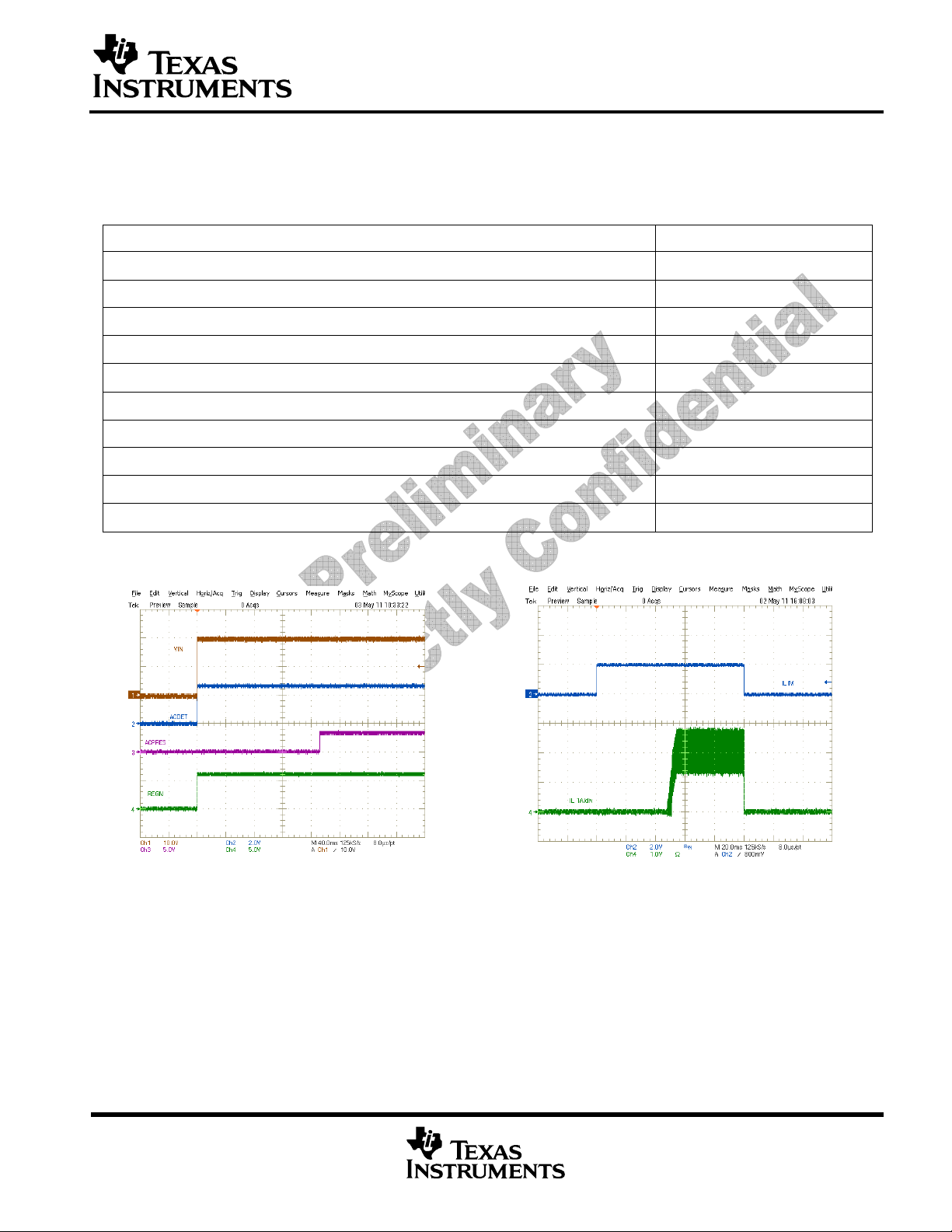
Figure 4. VCC, ACDET, REGN and ACPRES Power
Up
CH1: VCC, 10V/div, CH2: ACDET, 2V/div, CH3:
ACPRES, 5V/div, CH4: REGN, 5V/div, 40ms/div
12
Figure 5. Charge Enable by ILIM
CH2: ILIM, 2V/div, CH4: inductor current, 1A/div, 20ms/div
WWW.TI.COM

bq24728 DATASHEET
JUN 21, 2011
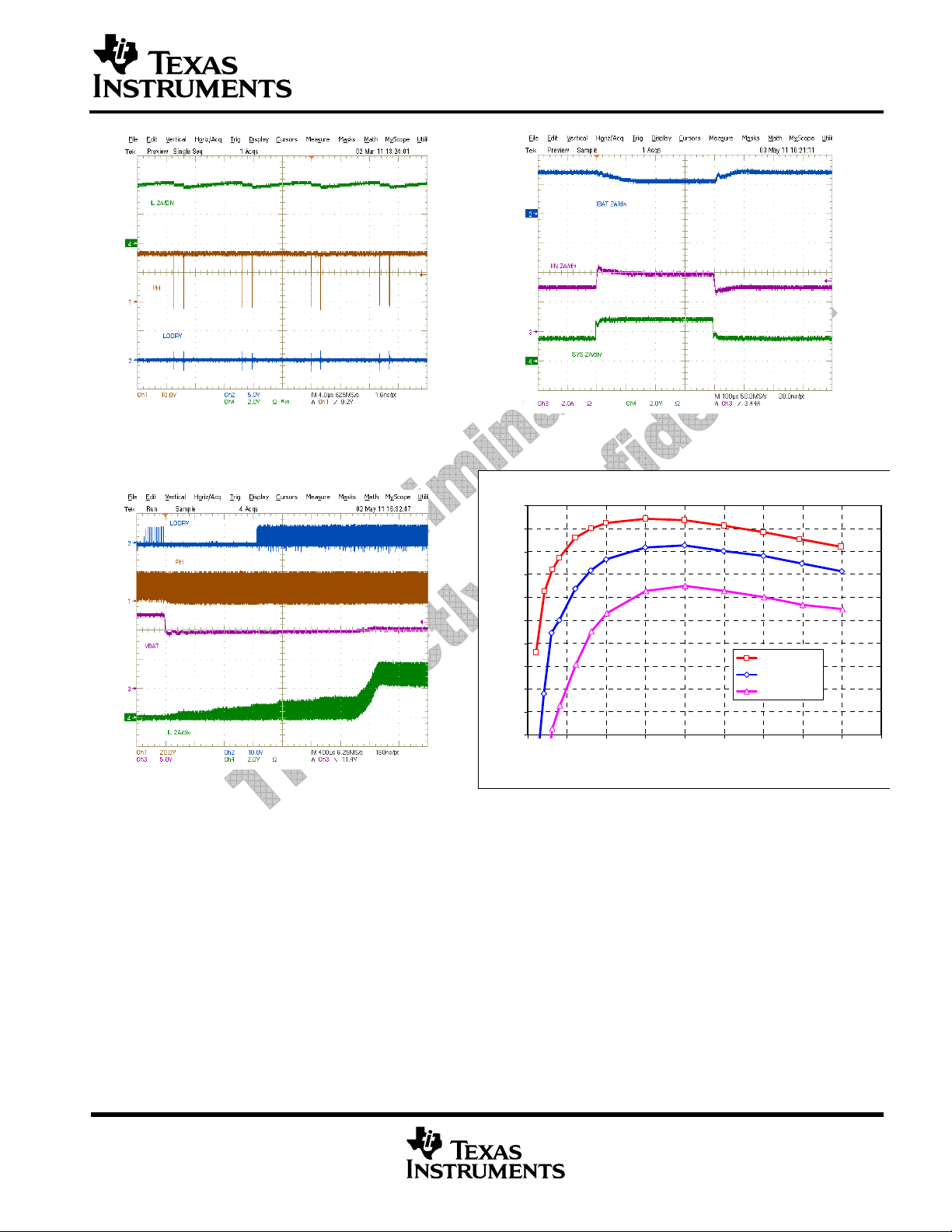
Figure 6. Current Soft-Start
CH1: PHASE, 20V/div, CH2: LODRV, 10V/div, CH3:
Vin, 5V/div, CH4: inductor current, 2A/div, 2ms/div
Figure 8. Continuous Conduction Mode Switching
Waveforms
CH1: PHASE, 10V/div, CH2: LODRV, 5V/div, CH3:
HIDRV, 10V/div, CH4: inductor current, 2A/div,
400ns/div
Figure 7. Charge Disable by ILIM
CH2: ILIM, 2V/div, CH4: inductor current, 1A/div, 4us/div
Figure 9. Cycle-by-Cycle Synchronous to Non-
synchronous
CH1: PHASE, 10V/div, CH2: LODRV, 5V/div, CH3:
HIDRV, 10V/div, CH4: inductor current, 1A/div, 400ns/div
WWW.TI.COM
13
bq24728 DATASHEET
JUN 21, 2011
Figure 10. 100% Duty and Refresh Pulse
CH1: PHASE, 10V/div, CH2: LODRV, 5V/div, CH4:
inductor current, 2A/div, 4us/div
Figure 12. Battery Insertion
CH1: PHASE, 20V/div, CH2: LODRV, 10V/div, CH3:
battery voltage, 5V/div, CH4: inductor current,
2A/div, 400us/div
Figure 11. System Load Transient (Input DPM)
CH2: battery current, 2A/div, CH3: adapter current, 2A/div,
CH4: system load current, 2A/div, 100us/div
VIN=20V, F=750k Hz, L=4. 7uH
98
97
96
95
94
93
92
Efficiency (%)
91
90
89
88
0 0.5 1 1.5 2 2.5 3 3.5 4 4.5
Charge Current
4-cell 16 . 8V
3-cell 12 . 6V
2-cell 8.4V
Figure 13. Efficiency vs Output Current
14
WWW.TI.COM
 Loading...