

Page 1

User's Guide
SLUU237 – January 2006
bq24720/21 EVM (HPA104) for Multi-Cell Synchronous
Switch-Mode Charger With System Power Selector and
SMBus SBS-Like Interface
Contents
1 Introduction .......................................................................................... 2
2 Test Summary ...................................................................................... 4
3 Circuit Design and Layout Guideline ........................................................... 21
4 Bill of Materials, Board Layout, and Schematics .............................................. 22
List of Figures
1 Connections of the EV2300 Kit ................................................................... 5
2 Original Test Setup for bq24720 EVM ........................................................... 6
3 Original Test Setup for bq24721 EVM ........................................................... 7
4 The Main Window of the bq2472x SMB Evaluation Software ................................ 8
5 The Software Main Window ....................................................................... 9
6 The Software Main Window ..................................................................... 10
7 The Software Main Window ..................................................................... 11
8 The Waveforms at No Load ..................................................................... 12
9 Test Setup for bq24720 EVM .................................................................... 13
10 Test Setup for bq24721 EVM .................................................................... 13
11 The Software Main Window ..................................................................... 14
12 The Waveforms at I
13 The Software Main Window ..................................................................... 16
14 The Software Main Window ..................................................................... 17
15 The Waveforms at I
16 The Software Main Window ..................................................................... 19
17 The Software Main Window ..................................................................... 20
18 Top Assembly ..................................................................................... 24
19 Bottom Assembly .................................................................................. 25
20 Layer 1.............................................................................................. 26
21 Layer 2.............................................................................................. 27
22 Layer 3.............................................................................................. 28
23 Layer 4.............................................................................................. 29
24 Top Silk ............................................................................................. 30
= 3 A .................................................................... 15
(bat)
= 300 mA ............................................................... 18
(bat)
SLUU237 – January 2006 bq24720/21 EVM (HPA104) for Multi-Cell Synchronous 1
Switch-Mode Charger With System Power Selector and SMBus SBS-Like Interface
Page 2

www.ti.com
Introduction
1 Introduction
1.1 EVM Features
1.2 General Description
• Evaluation Module For Both bq24720 and bq24721
• High Efficiency NMOS-NMOS Synchronous Buck Charger With User-Selectable 300 kHz or 500 kHz
Frequency
• Battery/Adapter to System Power Selector Function
• SBS-Like SMBus Interface for Control and Status Communications With Host
• Programmable Battery Voltage, Charge Current, and AC Adapter Current via SBS-Like SMBus
Interface
• Battery Pack Voltage Regulation Range up to 19.2 V
• AC Adapter Operating Range 13 V–24 V
• Charge and Adapter Overcurrent Protection
• Charge Peak Current up to 14 A. Charge Average Current up to 7 A
• LED Indication for AC Adaptor Connection, Power Path Conduction, Charge Enable and Alarm Signal
• Test Points for Key Signals Available for Testing Purpose. Easy Probe Hook-up
• Jumpers Available. Easy to Change Connections and Enable (or Disable) Charge
• May Be Used with TI bq2472x SMB Evaluation Software
The bq24720/21 evaluation module is a complete charger module for evaluating a multi-cell synchronous
notebook charge and path selection solution using the bq24720/21 devices. It is designed to deliver up to
9 A of charge current to Li-Ion or Li-Pol applications.
The bq24720/21 has a highly integrated battery charge controller designed to work with external host
commands. The battery voltage, charge current, and other system parameters are programmable via
SBS-like SMBus interface.
The dynamic power management (DPM) function SMBus Interface modifies the charge current depending
on system load conditions, avoiding ac adapter overload.
High accuracy current sense amplifiers enable accurate measurement of either the charge current or the
ac adapter current, allowing termination of nonsmart packs and monitoring of overall system power.
The adapter isolation diode can be bypassed with external an MOSFET using a control signal provided by
the bq24720/21, thus reducing overall power dissipation.
For details, see the bq24720 data sheet (SLUS668 ) and the bq24721 data sheet (SLUS683 ).
1.3 I/O Description
Jack Description
J1–POS AC adapter, positive output
J1–GND AC adapter, negative output
J2–POS External power supply, positive output
J2–GND External power supply, negative output
J3–REF VREF5 pin (11) output
J3–CHGEN CHGEN pin (1) output
J3–SDA SDA pin (13) output, SMBus data line
J3–SCL SCL pin (14) output, SMBus clock line
J4–ALARM ALARM pin (25) output
J4–IOUT IOUT pin (17) output
J4–GND Ground
2 bq24720/21 EVM (HPA104) for Multi-Cell Synchronous SLUU237 – January 2006
Switch-Mode Charger With System Power Selector and SMBus SBS-Like Interface
Page 3
www.ti.com
Jack Description
J5–REF IC reference voltage VREF5 (pin 11)
J5–VPUP Pull-up voltage source
J5–EXT External power supply
J6–CHGEN CHGEN pin (1) output
J6–GND Ground
J7–VPUP Pull-up voltage source
J7–LEDPWR LED Pull-up power line
J8–ACGD/TS ACGOOD pin (15) output for bq24720, TS pin (15) output for bq24721
J8–GND Ground
J8–VBAT Connected to battery pack
J8–VSYS Connected to system
J9–BYPASS BYPASS pin (6) output
J9–LED LED drive
J10–ACDRV ACDRV pin (2) output
J10–LED LED drive
J11–BATDRV BATDRV pin (24) output
J11–LED LED drive
J12–ACGD ACGOOD pin (15) output
J12–LED LED drive
Introduction
1.4 Controls and Key Parameters Setting
Jack or Resistor Description Factory Setting
Pull-up power source setting
J5 1-2: Use external power supply as the pull-up source
2-3: Use REF5 as the pull-up source
J6 Enable charge process when ON. Off
J7 On
The pull-up power source supplies the LEDs when ON. LED has no power source when
OFF.
J9 The conduction of the bypass MOSFET is indicated by D8 when ON. On
J10 The conduction of the AC MOSFET is indicated by D10 when ON. On
J11 The conduction of the battery MOSFET is indicated by D11 when ON. On
1.5 Recommended Operating Conditions
SYMBOL DESCRIPTION MIN TYP MAX UNIT
V
V
I
O
I
(chrg)
T
Supply voltage Input voltage from ac adapter input 13 19.5 24 V
I
Battery voltage Voltage applied at VBAT terminal of J8 9–16.8 20 V
(BAT)
Supply current Maximum input current from ac adapter input 5 7 A
Charge current Battery charge current 2 4 7 A
Operating junction temperature range 0 125 ° C
J
1-2 (pin 1 and 2
are short-circuited)
SLUU237 – January 2006 bq24720/21 EVM (HPA104) for Multi-Cell Synchronous 3
Switch-Mode Charger With System Power Selector and SMBus SBS-Like Interface
Page 4

www.ti.com
Test Summary
2 Test Summary
2.1 Definitions
This procedure details the configure of the HPA104 evaluation board. On the test procedure, the following
naming conventions are followed. See the HPA104 schematic for details.
VXXX : External voltage supply name (VADP, VBT, VSBT)
LOADW: External load name (LOADR, LOADI)
V(TPyyy): Voltage at HPA104 internal test point TPyyy. For example, V(TP12) means the
voltage at TP12.
V(Jxx): Voltage at HPA104 jack terminal Jxx.
V(TP(XXX)): Voltage at test point XXX. For example, V(ACDET) means the voltage at the
test point which is marked as ACDET.
V(XXX, YYY): Voltage across point XXX and YYY.
I(JXX(YYY)): Current going out from the YYY terminal of jack XX.
Jxx(BBB): Terminal or pin BBB of jack xx
Jxx ON : HPA104 internal jumper Jxx terminals are shorted
Jxx OFF: HPA104 internal jumper Jxx terminals are open
Jxx (-YY-) ON: HPA104 internal jumper Jxx adjacent terminals marked as YY are shorted
Measure → A,B Check specified parameters A, B. If measured values are not within specified
limits, the unit under test has failed.
Observe → A,B Observe if A, B occurs. If they do not occur, the unit under test has failed.
The assembly drawings have locations for jumpers, test points, and individual components.
2.2 Equipment
2.2.1 POWER SUPPLIES
• Power Supply Number 1 (PS1): a power supply capable of supplying 20-V at 5-A is required.
• Power Supply Number 2 (PS2): a power supply capable of supplying 5-V at 1-A is required.
• Power Supply Number 3 (PS3): a power supply capable of supplying 5-V at 1-A is required. (bq24721
EVM only).
2.2.2 ELECTRONIC LOAD
• A 30-V, 5-A electronic load
2.2.3 KEPCO LOAD
• A Kepco bipolar operational power supply / amplifier, 0 V ± 20 V (or above), 0 A ± 6 A (or above).
2.2.4 METERS
• Eight Fluke 75, (equivalent or better)
– Or: Five equivalent voltage meters and three equivalent current meters. The current meters must
be able to measure 5A+ current.
2.2.5 OSCILLOSCOPES
• An oscilloscope, a single voltage probe, and a single current probe are required.
bq24720/21 EVM (HPA104) for Multi-Cell Synchronous4 SLUU237 – January 2006
Switch-Mode Charger With System Power Selector and SMBus SBS-Like Interface
Page 5
www.ti.com
2003
EV2300
HPA002
VCC
HDQ
VOUT
GND
VOUT
SDA
SCL
GND
NC
SMBD
SMBC
GND
HDQI2C
SMB
USB
To Computer
USB port
SDA
SCL
GND
To EVM
2003
EV2300
HPA002
VCC
HDQ
VOUT
GND
VOUT
SDA
SCL
GND
NC
SMBD
SMBC
GND
HDQI2C
SMB
USB
To Computer
USB port
SDA
SCL
GND
To EVM
2.2.6 COMPUTER
• A computer with at least one USB port and a USB cable. The EV2300 USB driver and the bq2472x
SMB evaluation software must be properly installed.
2.2.7 EV2300 SMBUS COMMUNICATION KIT
• An EV2300 SMBUS communication kit.
2.2.8 SOFTWARE
• Driver(USB EV2300) Installer XP2K-Last updated Jan 28-04.zip: This is the EV2300 USB driver. Save
and unzip to c:\temp (or other directory). Double click on the setup.exe file. Follow the installation
steps.
• bq24720SMBEVSW2_10.zip: This is the bq2472x SMB evaluation software. Save and unzip to c:\temp
(or other directory). Double click on the SETUP.EXE file. Follow the installation steps. This software
needs to be installed after the EV2300 USB driver.
2.3 Equipment Setup
1. Set the power supply number 1 for 0 V ± 100 mVDC, 5 A ± 0.1 A current limit and then turn off the
supply.
2. Connect the output of power supply number 1 in series with a current meter (multimeter) to J1 (POS,
GND).
3. Connect a voltage meter across J1 (POS, GND).
4. Set the power supply number 2 for 3.3 V ± 100 mVDC, 1 A ± 0.1 A current limit and then turn off the
supply.
5. Connect the output of the power supply number 2 to J2 (POS, GND).
6. Set the Kepco load for 10 V ± 100 mVDC and then turn it off.
7. Turn off the electronic load.
8. Connect a voltage meter across J8 (VBAT, GND).
9. Connect a voltage meter across J8 (VSYS, GND).
10. Connect J3 (SDA, SCL) and J4 (GND) to the EV2300 kit SMB port. Connect the USB port of the
EV2300 kit to the USB port of the computer. The connections are shown in Figure 1 .
Test Summary
SLUU237 – January 2006 bq24720/21 EVM (HPA104) for Multi-Cell Synchronous 5
11. Turn on the oscilloscope.
12. Insert the voltage probe into TP30 (PH) and connect it to the oscilloscope.
13. Hook up the current probe to the wire connected to L1, and connect to the oscilloscope. Set up the
Figure 1. Connections of the EV2300 Kit
current probe so that the current direction is from the floating pad to the pad on the right-hand side.
14. J5 (VPUP, EXT): ON, J6: OFF, J7: ON, J9: ON J10: ON, J11: ON.
15. J12: ON ( For bq24720 only), J12: OFF ( For bq24721 only).
Switch-Mode Charger With System Power Selector and SMBus SBS-Like Interface
Page 6
www.ti.com
V
POS
J1
GND
VSYS
J8
GND
VBAT
IOUT
GND
REF
J3
J2
J11J10J9
J7
Power
supply #2
ACGD
J4
GND
ALARM
CHGEN
SDA
SCL
POS
J6
J5
D8 D10 D11 D7 D9
D18
J12
APPLICATION CIRCUIT
V
USB
V
EV2300
Iin
I
Power
supply #1
BQ24720 EVM
Oscilloscope
L1
PH
V
POS
J1
GND
VSYS
J8
GND
VBAT
IOUT
GND
REF
J3
J2
J11J10J9
J7J7J7
Power
supply #2
ACGD
J4
GND
ALARM
CHGEN
SDA
SCL
POS
J6J6J6
J5
D8 D10 D11 D7 D9
D18
J12
APPLICATION CIRCUIT
V
USB
V
EV2300
Iin
I
Power
supply #1
BQ24720 EVM
Oscilloscope
L1
PH
Test Summary
16. ( For bq24721 only) Set the power supply number 3 for 2.5 V ± 100 mVDC, 1 A ± 0.1 A current limit
and then turn off the supply.
17. ( For bq24721 only) Connect the output of the power supply number 3 to J8 (ACGD, GND).
After the steps above, the test setup for bq24720 EVM is shown in Figure 2 . The test setup for bq24721
EVM is shown in Figure 3 .
Figure 2. Original Test Setup for bq24720 EVM
6 bq24720/21 EVM (HPA104) for Multi-Cell Synchronous SLUU237 – January 2006
Switch-Mode Charger With System Power Selector and SMBus SBS-Like Interface
Page 7
www.ti.com
V
POS
J1
GND
VSYS
J8
GND
VBAT
IOUT
GND
REF
J3
J2
J11J10J9
J7
Power
supply #2
ACGD
J4
GND
ALARM
CHGEN
SDA
SCL
POS
J6
J5
D8 D10 D11 D7 D9
D18
J12
APPLICATION CIRCUIT
V
USB
V
EV2300
Iin
I
Power
supply #1
BQ24721 EVM
Oscilloscope
L1
PH
V
Power
supply #3
V
POS
J1
GND
VSYS
J8
GND
VBAT
IOUT
GND
REF
J3
J2
J11J10J9
J7J7J7
Power
supply #2
ACGD
J4
GND
ALARM
CHGEN
SDA
SCL
POS
J6J6J6
J5
D8 D10 D11 D7 D9
D18
J12
APPLICATION CIRCUIT
V
USB
V
EV2300
Iin
I
Power
supply #1
BQ24721 EVM
Oscilloscope
L1
PH
V
Power
supply #3
Test Summary
Figure 3. Original Test Setup for bq24721 EVM
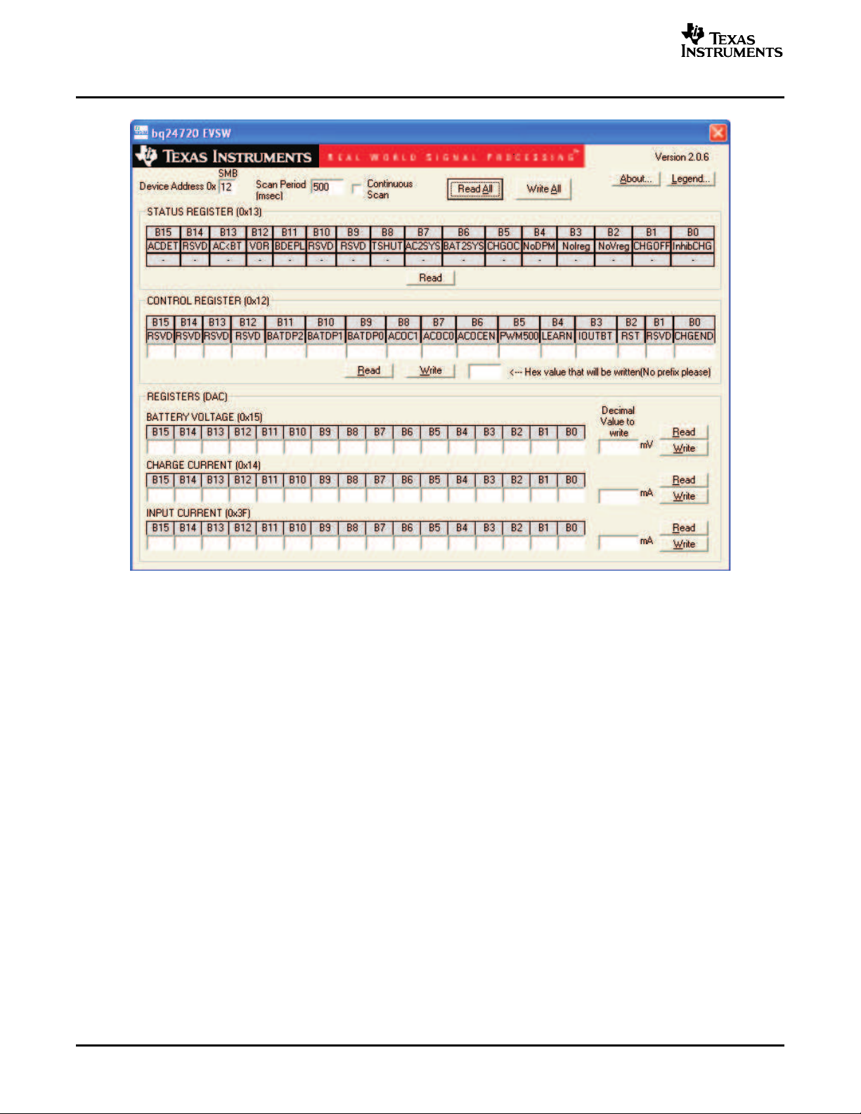
Turn on the computer. Open the bq2472x SMB evaluation software. The main window of the software is
shown in Figure 4 .
SLUU237 – January 2006 bq24720/21 EVM (HPA104) for Multi-Cell Synchronous 7
Switch-Mode Charger With System Power Selector and SMBus SBS-Like Interface
Page 8
www.ti.com
Test Summary
Figure 4. The Main Window of the bq2472x SMB Evaluation Software
2.4 Procedure
2.4.1 AC Adapter Detection Threshold
Make sure EQUIPMENT SETUP steps are followed. Turn on PS2
( For bq24721 only) Turn on PS3
Turn on PS1
Measure→ V(J8(VSYS)) = 0 V ± 500 mV
Measure→ V(TP(VREF5)) = 0 V ± 500 mV
Increase the output voltage of PS1 until the D8 (BYPASS) is on. The threshold is approximately 13 V. Do
not exceed.
Measure→ V(TP(ACDET)) = 1.2 V ± 0.1 V
Measure→ V(J1(POS)) = 13 V ± 1 V
Measure→ V(J8(VSYS)) = 13 V ± 1 V
Measure→ V(TP(VREF5)) = 5 V ± 500 mV
Measure→ V(TP20) = 6 V ± 200 mV (TP20 is a through-hole test point above the IC)
Observe→ D18 (ACGOOD) on ( for bq24720 only)
Observe→ D10 (ACSW) ON, D9 (ALARM) ON
bq24720/21 EVM (HPA104) for Multi-Cell Synchronous8 SLUU237 – January 2006
Switch-Mode Charger With System Power Selector and SMBus SBS-Like Interface
Page 9
www.ti.com
2.4.2 Charge Parameters Setting
Increase the voltage of PS1 until V(J1(POS)) = 19 V ± 0.1 V.
Measure→ V(J8(VBAT, GND)) = 0 V ± 1 V
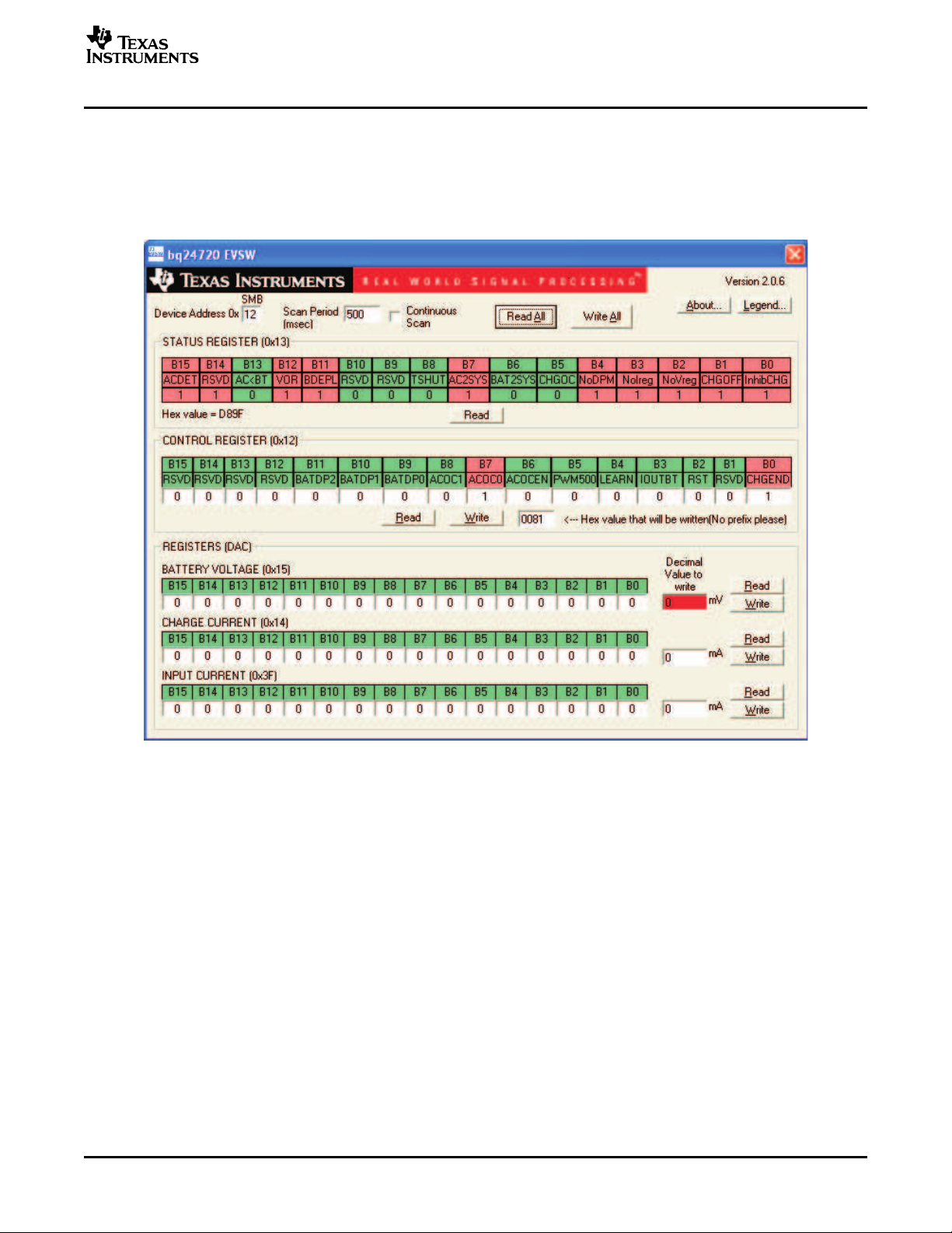
In the software main window, click Read All on the top part of the window. The window is shown in
Figure 5 .
Test Summary
Figure 5. The Software Main Window
Type 12600 (mV) in the Battery Voltage Register on the lower right part of the window and click Write.
This sets the battery voltage regulation threshold.
Type 1000 (mA) in the Charge Current Register on the lower right part of the window and click Write. This
sets the battery charge current regulation threshold.
Type 5000 (mA) in the Input Current Register on the lower right part of the window and click Write. This
sets the input current regulation threshold.
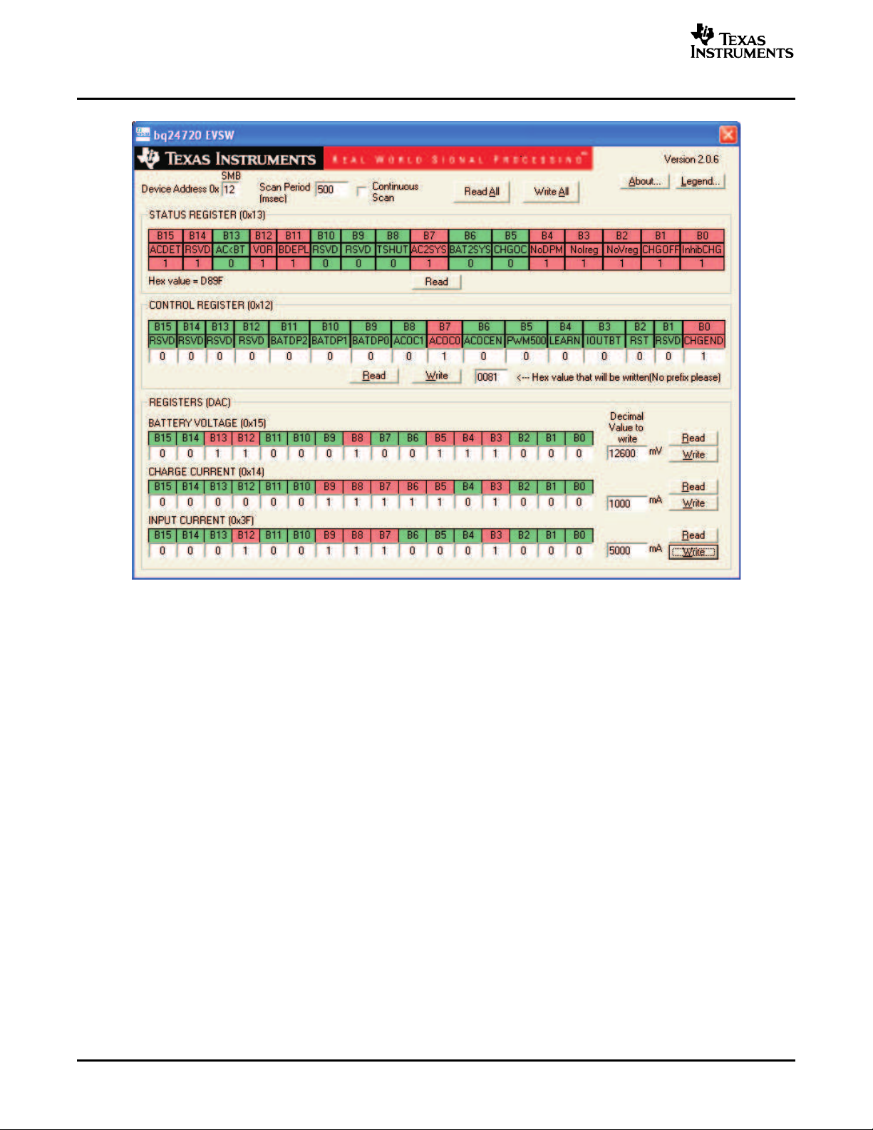
The window should be like Figure 6 .
SLUU237 – January 2006 bq24720/21 EVM (HPA104) for Multi-Cell Synchronous 9
Switch-Mode Charger With System Power Selector and SMBus SBS-Like Interface
Page 10
www.ti.com
Test Summary
Figure 6. The Software Main Window
Install J6.
Observe→ D7 (CHG EN) ON.
Change the B0 bit (CHGEND) of Control Register to 0. (Enable the charging). Click Write.
Measure→ V(J8(VBAT)) = 12.6 V ± 200 mV
Observe→ D9 (ALARM) ON.
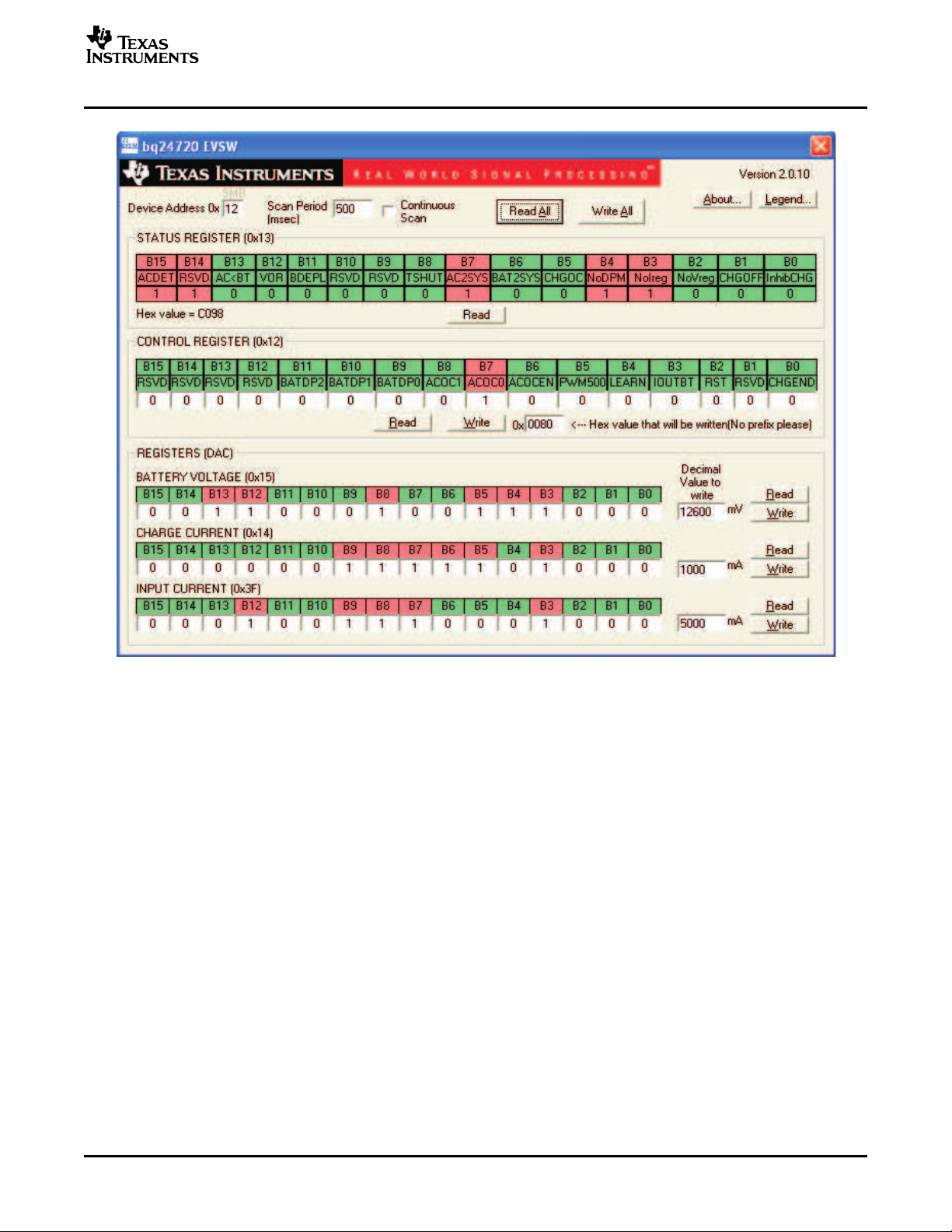
In the software main window, click Read All on the top part of the window.
Observe→ D9 (ALARM) off.
Observe→ The B2 bit (NoVreg) of the Status Register turns green (voltage loop active). The window
should be like Figure 7 .
10 bq24720/21 EVM (HPA104) for Multi-Cell Synchronous SLUU237 – January 2006
Switch-Mode Charger With System Power Selector and SMBus SBS-Like Interface
Page 11
www.ti.com
Test Summary
Figure 7. The Software Main Window
Observe → Make sure the phase node voltage (PH) and the inductor current waveforms look like
Figure 8 .
SLUU237 – January 2006 bq24720/21 EVM (HPA104) for Multi-Cell Synchronous 11
Switch-Mode Charger With System Power Selector and SMBus SBS-Like Interface
Page 12

www.ti.com
Test Summary
Figure 8. The Waveforms at No Load
2.4.3 Charge Current and AC Current Regulation (DPM)
Change the B0 bit (CHGEND) of Control Register to 0. (Enable the charging). Click Write.
Connect the output of the Kepco load in series with a current meter (multimeter) to J8 (VBAT, GND).
Make sure a voltage meter is connected across J8 (VBAT, GND). Turn on the Kepco load. Connect the
output of the electronic load in series with a current meter (multimeter) to J8 (VSYS, GND). Make sure a
voltage meter is connected across J8 (VSYS, GND). Turn on the power of the electronic load. Set the load
current to 2.5 A ± 50 mA, but disable the output. The setup is now like Figure 9 for bq24720 and like
Figure 10 for bq24721. Make sure I
= 0 A ± 10 mA and I
(bat)
(sys)
= 0 A ± 10 mA.
12 bq24720/21 EVM (HPA104) for Multi-Cell Synchronous SLUU237 – January 2006
Switch-Mode Charger With System Power Selector and SMBus SBS-Like Interface
Page 13

www.ti.com
BQ24720 EVM
Ibat
V
I
POS
J1
GND
VSYS
J8
GND
VBAT
IOUT
GND
REF
J3
J2
J11J10J9
J7
Power
supply #2
ACGD
J4
GND
ALARM
CHGEN
SDA
SCL
POS
J6
J5
D8 D10 D11 D7 D9
APPLICATION CIRCUIT
Isys
V
I
USB
V
EV2300
Electr.
Load
Kepco
Load
Iin
I
Power
supply #1
D18
J12
Oscilloscope
L1
PH
BQ24720 EVM
Ibat
V
I
POS
J1
GND
VSYS
J8
GND
VBAT
IOUT
GND
REF
J3
J2
J11J10J9
J7J7J7
Power
supply #2
ACGD
J4
GND
ALARM
CHGEN
SDA
SCL
POS
J6J6J6
J5
D8 D10 D11 D7 D9
APPLICATION CIRCUIT
Isys
V
I
USB
V
EV2300
Electr.
Load
Kepco
Load
Iin
I
Power
supply #1
D18
J12
Oscilloscope
L1
PH
BQ24721 EVM
Ibat
V
I
POS
J1
GND
VSYS
J8
GND
VBAT
IOUT
GND
REF
J3
J2
J11J10J9
J7
Power
supply #2
ACGD
J4
GND
ALARM
CHGEN
SDA
SCL
POS
J6
J5
D8 D10 D11 D7 D9
APPLICATION CIRCUIT
Isys
V
I
USB
V
EV2300
Electr.
Load
Kepco
Load
Iin
I
Power
supply #1
D18
J12
Oscilloscope
L1
PH
V
Power
supply #3
BQ24721 EVM
Ibat
V
I
POS
J1
GND
VSYS
J8
GND
VBAT
IOUT
GND
REF
J3
J2
J11J10J9
J7J7J7
Power
supply #2
ACGD
J4
GND
ALARM
CHGEN
SDA
SCL
POS
J6J6J6
J5
D8 D10 D11 D7 D9
APPLICATION CIRCUIT
Isys
V
I
USB
V
EV2300
Electr.
Load
Kepco
Load
Iin
I
Power
supply #1
D18
J12
Oscilloscope
L1
PH
V
Power
supply #3
Test Summary
Figure 9. Test Setup for bq24720 EVM
SLUU237 – January 2006 bq24720/21 EVM (HPA104) for Multi-Cell Synchronous 13
Figure 10. Test Setup for bq24721 EVM
Switch-Mode Charger With System Power Selector and SMBus SBS-Like Interface
Page 14

www.ti.com
Test Summary
Change the B0 bit (CHGEND) of Control Register to 0. (Enable the charging). Click Write.
Measure→ I
= 1000 mA ± 200 mA
(bat)
Type in 3000 (mA) in the Charge Current Register and click Write.
Measure→ I
= 3000 mA ± 200 mA
(bat)
Make sure the B3 bit (IOUTBT) of the Control Register is 1. (charge current output). If not, change it to 1.
Click Write.
Measure→ V(J4(IOUT)) = 600 mV ± 30 mV
Click Read All.
Observe→ The B3 bit (NoIreg) of the Status Register turns green (charge current loop active). The
window should be like Figure 11 .
Figure 11. The Software Main Window
Observe→ Make sure the phase node voltage and the inductor current waveforms look like Figure 12 .
14 bq24720/21 EVM (HPA104) for Multi-Cell Synchronous SLUU237 – January 2006
Switch-Mode Charger With System Power Selector and SMBus SBS-Like Interface
Page 15

www.ti.com
Test Summary
Figure 12. The Waveforms at I
= 3 A
(bat)
Enable the output of the electronic load.
Measure→ I
= 2500 mA ± 200 mA, I
(sys)
= 3000 mA ± 200 mA, II= 4300 mA ± 300 mA
(bat)
Disable the output of the electronic load.
Type 3000 (mA) in the Input Current Register and click Write.
Enable the output of the electronic load.
Measure→ I
= 2500 mA ± 200 mA, I
(sys)
= 500 mA ± 300 mA, II= 3000 mA ± 400 mA
(bat)
Measure→ V(J4(IOUT)) = 100 mV ± 80 mV
Change the B3 bit (IOUTBT) of the Control Register to 0. (adapter current output). Click Write.
Measure→ V(J4(IOUT)) = 600 mV ± 30 mV
Click Read All
Observe→ The B4 bit (NoDPM) of the Status Register turns green (DPM loop active). The window
should be like Figure 13 .
SLUU237 – January 2006 bq24720/21 EVM (HPA104) for Multi-Cell Synchronous 15
Switch-Mode Charger With System Power Selector and SMBus SBS-Like Interface
Page 16

www.ti.com
Test Summary
Figure 13. The Software Main Window
Turn off the electronic load.
Measure→ I
= 0 ± 100 mA, I
(sys)
= 3000 mA ± 200 mA.
(bat)
2.4.4 Charger Cut-Off by Thermistor (bq24721 ONLY)
Slowly increase the output voltage of PS3 until I
(bat)
= 0 A ± 10 mA.
Measure→ V(J8(ACGD)) = 3.675 V ± 300 mV
Slowly decrease the output voltage of PS3. Charge resumes. Continue to decrease the output voltage of
PS3 until I
(bat)
= 0 A ± 10 mA.
Measure→ V(J8(ACGD)) = 1.465 V ± 300 mV
Slowly increase the output voltage of PS3 to 2.5 V ± 100 mV
Measure→ I
= 3000 mA → 200 mA.
(bat)
2.4.5 Voltage Regulation and NonSynchronous Operation at Light Load
Slowly increase the output voltage of the Kepco load until I
(bat)
Measure→ V(J8(VBAT, GND)) = 12.6 V ± 200 mV
In the Software main window, click Read All.
Observe → The B2 bit (NoVreg) of the Status Register turns green (voltage loop active). The window
should be like Figure 14 .
= 300 mA ± 20 mA
16 bq24720/21 EVM (HPA104) for Multi-Cell Synchronous SLUU237 – January 2006
Switch-Mode Charger With System Power Selector and SMBus SBS-Like Interface
Page 17

www.ti.com
Test Summary
Figure 14. The Software Main Window
Observe→ The inductor current waveform is like Figure 15 . The inductor current does not drop below
0 A.
SLUU237 – January 2006 bq24720/21 EVM (HPA104) for Multi-Cell Synchronous 17
Switch-Mode Charger With System Power Selector and SMBus SBS-Like Interface
Page 18

www.ti.com
Test Summary
2.4.6 Learn Cycle
Change the B0 bit (CHGEND) of the Control Register to 1 (disable the charging). Click Write.
Change the B4 bit (LEARN) of the Control Register to 1. (learn cycle). Click Write.
Figure 15. The Waveforms at I
(bat)
Measure→ V(J8(VSYS)) = 19 V ± 1 V (adapter connected to system)
Observe→ D10 (ACSW ON) ON, D11 (BATDRV ON) OFF.
Measure→ V(J8(VSYS)) = 12.3 V ± 300 mV (battery connected to system).
Observe→ D10 (ACSW ON) off, D11 (BATDRV ON) ON.
Click Read All.
Observe→ The window should be like Figure 16 .
= 300 mA
18 bq24720/21 EVM (HPA104) for Multi-Cell Synchronous SLUU237 – January 2006
Switch-Mode Charger With System Power Selector and SMBus SBS-Like Interface
Page 19

www.ti.com
Test Summary
2.4.7 Power Path Selection
Change the B4 bit (LEARN) of the Control Register to 0. (no learn). Click Write.
Measure→ V(J8(VSYS)) = 19 V ± 1 V (adapter connected to system)
Observe→ D10 (ACSW ON) ON, D11 (BATDRV ON) OFF.
Turn off PS1.
Measure→ V(J8(VSYS)) = 12.3 V ± 300 mV (battery connected to system)
Observe→ D10 (ACSW ON) OFF, D11 (BATDRV ON) ON, D8 (BYPASS ON) OFF.
Observe→ The B1 bit (CHGOFF) of the Status Register turns red (charger is not on). The window
should be like Figure 17 .
Figure 16. The Software Main Window
SLUU237 – January 2006 bq24720/21 EVM (HPA104) for Multi-Cell Synchronous 19
Switch-Mode Charger With System Power Selector and SMBus SBS-Like Interface
Page 20

www.ti.com
Test Summary
Figure 17. The Software Main Window
bq24720/21 EVM (HPA104) for Multi-Cell Synchronous20 SLUU237 – January 2006
Switch-Mode Charger With System Power Selector and SMBus SBS-Like Interface
Page 21

www.ti.com
3 Circuit Design and Layout Guideline
3.1 Optional Components
The bq24720/21 EVM has all components required for robust operation on a wide range of different
operating conditions and ac adapter/load transients. However, some of its components might not be
required, or can be of distinct value, depending on the application condition. See the bq24720/21
application notes for details.
Component When it must be added to application circuit
D2/R8 Turn-on time for the bypass switch Q1 must be increased.
D3/R12 Turn-on time for the ac switch Q2 must be increased.
D6/R24 Turn-on time for the battery switch Q5 must be increased.
C17/C19 Switching time for the ac switch Q2 must be increased.
R16/R17
R19 Switching time for the switch Q4 must be increased.
C22/C24/C28/C29 These capacitors are always required for PWM ripple current filtering. The value may be decreased as long
value as the low current ripple, low transient voltage spike, and loop response stability can be assured.
(1)
(1)
Use bootstrap resistor R16 to adjust the switching time of the high-side switch. Do not use high-side and low-side gate resistors.
The high-side gate resistor R17 must be lower than 5 Ω to assure the break-before-make.
3.2 Layout Tips
1. The control stage and the power stage are layed out separately. At each layer, the signal ground and
the power ground are connected only at the power pad with a single point underneath the IC.
2. the ac current sense resistor must be connected to the ACP (pin 4) and ACN (pin 3) by Kelvin contact.
The area of this loop must be minimized. The decoupling capacitors for these pins should be placed as
close as possible to the IC .
3. the charge current sense resistor must be connected to SRP (pin 20), SRN (pin 19), SYNP (pin 22)
and SYNN (pin 21) by Kelvin contact. The area of this loop must be minimized. The decoupling
capacitors for these pins should be placed as close as possible to the IC .
4. The decoupling capacitors for the VCC (pin 12), VREF5 (pin 11), REGN (pin 28) should be placed
underneath the IC (on the bottom layer). Make the interconnections to the IC as short as possible.
5. The decoupling capacitors for BAT (pin 18), IOUT (pin 17) must be placed close to the corresponding
IC pins. Make the interconnections to the IC as short as possible.
6. C17 and C19, if used, must be placed as close as possible to Q2 (AC switch) .
7. The decoupling capacitor (C15) for the charger input must be placed close to Q3 drain and Q4 source.
Circuit Design and Layout Guideline
Switching time for the switch Q3 must be increased.
SLUU237 – January 2006 bq24720/21 EVM (HPA104) for Multi-Cell Synchronous 21
Switch-Mode Charger With System Power Selector and SMBus SBS-Like Interface
Page 22

www.ti.com
Bill of Materials, Board Layout, and Schematics
4 Bill of Materials, Board Layout, and Schematics
4.1 Bill of Materials
bq24720 bq24721
-001 -002
15 15 C21, C25, C26, 0.1 µ F Capacitor, Ceramic, 0.1- µ F, 50-V, X7R, 10% 0805 C0805C104K5RACTU Kemet
7 7 C14, C23, C31, 10 µ F Capacitor, Ceramic, 50V, 10 µ F, 20%/+80% 1210 ECJ-4YF1H106Z
1 1 C11 2000 pF Capacitor, Ceramic, 2000pF, 50-V, C0G, 5% 0805 GRM2165C1H202JA01D Murata
2 2 C16, C18 1 µ F Capacitor, Ceramic, 1- µ F, 25-V, X7R, 10% 0805 C2012X7R1E105K TDK
1 1 C17 10 nF 0603 C0603C103K5RACTU Kemet
0 0 C19 Open Capacitor, Ceramic, Open, 50-V, X7R, 10% 0603
2 2 C2, C4 4.7 µ F Capacitor, Ceramic, 4.7- µ F, 50-V, X7R, 10% 1210 GRM32ER71H475KA88L Murata
4 4 10 µ F Capacitor, Ceramic, 10- µ F, 25-V, X5R, 20% 1206 ECJ-3YB1E106M
1 1 C8 51 pF Capacitor, Ceramic, 51-pF, 50-V, C0G, 5% 0603 GRM1885C1H510JA01D Murata
1 1 C9 130 pF Capacitor, Ceramic, 130-pF, 50-V, C0G, 5% 0603 GRM1885C1H131JA01D Murata
1 1 D1 Diode, Dual Schottky, 200-mA, 30-V SOT23 BAT54C Vishay-Liteon
3 3 D2, D3, D6 Diode, Switching, 10-mA, 85-V, 350-mW SOT23 BAS16 Vishay-Liteon
1 1 D4 Diode, Schottky, 200-mA, 30-V SOT23 BAT54 Vishay-Liteon
1 1 D5 Diode, Schottky, 1A, 30V SMB MBRS130TR IR
2 2 D7, D18 Diode, LED, Green, 2.1-V, 20-mA, 6-mcd 0603 160-1183-1-ND Liteon
3 3 D8, D10, D11 Diode, LED, Green, 20-mA, 0.9-mcd 0.068 × 0.049 LN1371G-(TR) Panasonic
1 1 D9 Diode, LED, Red, 1.8-V, 20-mA, 20-mcd 0603 160-1181-1-ND Liteon
1 1 J1 Terminal Block, 2-pin, 15-A, 5,1 mm 0.40 × 0.35 ED1609 OST
1 1 J2 Terminal Block, 2-pin, 6-A, 3,5 mm 75525 ED1514 OST
1 1 J3 Terminal Block, 4-pin, 6-A, 3,5 mm 0.55 × 0.25 ED1516 OST
1 1 J4 Terminal Block, 3-pin, 6-A, 3,5 mm 0.41 × 0.25 ED1515 OST
1 1 J5 Header, 3-pin, 100 mil spacing, (36-pin strip) 0.100 × 3 PTC36SAAN Sullins
6 6 Header, 2-pin, 100 mil spacing, (36-pin strip) 0.100 × 2 PTC36SAAN Sullins
1 1 J8 ED1516 Terminal Block, 4-pin, 15-A, 5,1 mm 0.80 x 0.35 ED2227 OST
1 1 L1 10uH Inductor, SMT, 10- µ H, 7A, 31- Ω 0.51 × 0.51 IHLP5050FDER100M01 Vishay
3 3 Q1, Q2, Q5 MOSFET, P-ch, 30-V, 8.0-A, 20- Ω SO8 Si4435DY Siliconix
1 1 Q3 SO8 FDS6680A Fairchild
1 1 Q4 SO8 FDS6670A Fairchild
3 3 Q6, Q12, Q17 SOT-23 TP0610K
8 8 Q11, Q13, Q15, MOSFET, N-ch, 60-V, 115-mA, 1.2- Ω SOT23 2N7002DICT Vishay-Liteon
1 1 R1 499k Resistor, Chip, 1/16W, 1% 0402 Std Std
2 2 R10, R22 0.01 Resistor, Chip, 0.010- Ω , 1/2-W, 2010 ± 1% WSL2010.010 Vishay - Dale
1 1 R11 200k Resistor, Chip, 1/16W, 1% 0402 Std Std
1 1 R13 20k Resistor, Chip, 1/16W, 1% 0402 Std Std
1 1 R14 7.5k Resistor, Chip, 1/16W, 1% 0402 Std Std
1 1 R16 15 Resistor, Chip, 1/16W, 5% 0402 Std Std
1 1 R18 33k Resistor, Chip, 1/16W, 1% 0402 Std Std
1 1 R2 49.9k Resistor, Chip, 1/16W, 1% 0402 Std Std
1 1 R20 5.62k Resistor, Chip, 1/16W, 1% 0402 Std Std
0 1 R21 118k Resistor, Chip, 1/16W, 1% 0402 Std Std
0 0 R23, R37 Open Resistor, Chip, 1/16W, 5% 0402 Std Std
6 6 100k Resistor, Chip, 100 k Ω , 1/10W, 5% 0805 Std Std
Ref Des Value Description Size Part Number MFR
C1, C3, C5, C6,
C7, C15, C20,
C27, C30, C33,
C34, C35
C10, C12, C13,
C32
Capacitor, Ceramic, 0.01- µ F, 50-V, X7R,
10%
C22, C24, C28, Panasonic C29 ECG
J6, J7, J9, J10,
J11, J12
Transistor, MOSFET, NChan, 30V, 12.5A,
Rds 9.5 Ω
Transistor, MOSFET, N-Chan, 30V, 13A, Rds
8 Ω
MOSFET, P-Ch, 60V, Rds 6 Ω , VishayId 185 mA Siliconix
Q7, Q8, Q9, Q10,
Q32
R25, R26, R32,
R33, R35, R36
Panasonic ECG
22 bq24720/21 EVM (HPA104) for Multi-Cell Synchronous SLUU237 – January 2006
Switch-Mode Charger With System Power Selector and SMBus SBS-Like Interface
Page 23

www.ti.com
Bill of Materials, Board Layout, and Schematics
bq24720 bq24721
-001 -002
2 2 R27, R30 20k Resistor, Chip, 20 k Ω , 1/10-W, 5% 0805 Std Std
6 6 2.2k Resistor, Chip, 1/10W, 5% 0805 Std Std
1 1 R3 20k Resistor, Chip, 1/16W, 5% 0402 Std Std
3 3 R4, R6, R9 5.1k Resistor, Chip, 1/16W, 5% 0402 Std Std
1 1 R5 100k Resistor, Chip, 1/16W, 5% 0402 Std Std
1 1 R7 1k Resistor, Chip, 1/16W, 5% 0402 Std Std
6 6 0 Resistor, Chip, 1/16W, 5% 0402 Std Std
7 7 SJ3,SJ4, SJ5, Shorting jumpers, 2-pin, 100mil spacing 929950-00 3M/ESD
4 4 6-32 NYL nuts
4 4 4816 STANDOFF M/F HEX 6-32 NYL 0.500" sf_thvt_325_rnd 4816 Keystone
18 18 5002 Test Point, White, Thru Hole Color Keyed 0.100 × 0.100" 5002 Keystone
4 4 0.2 131-4244-00
0 0 Test Point, 0.020 Hole"
4 4 5006 Test Point, Black, Thru Hole Compact Style 0.125 × 0.125 5006
1 0 U1 QFN-32 bq24720RHB TI
0 1 U1 QFN-32 bq24721RHB TI
Ref Des Value Description Size Part Number MFR
R28, R29, R31,
R34, R39, R65
R8, R12, R17,
R19, R24, R38
SJ1, SJ2,
SJ6, SJ7
ST1, ST2, ST3,
ST4
TP1, TP2, TP3,
TP4, TP5, TP6,
TP13, TP14,
TP19, TP22,
TP24, TP26,
TP27, TP29,
TP31, TP32,
TP42, TP43
TP15, TP30, Adaptor, 3.5-mm probe clip
TP45, TP46 ( or 131-5031-00)
TP7, TP9, TP10,
TP11, TP12,
TP16, TP17,
TP20, TP21,
TP23, TP25,
TP33, TP34,
TP35, TP36,
TP37, TP38,
TP39, TP40,
TP41, TP47
TP8, TP18, TP28,
TP44
IC, Advanced Multi Cell Synchronous
Charger and System Power Selector
IC, Advanced Multi Cell Synchronous
Charger and System Power Selector
SLUU237 – January 2006 bq24720/21 EVM (HPA104) for Multi-Cell Synchronous 23
Switch-Mode Charger With System Power Selector and SMBus SBS-Like Interface
Page 24

www.ti.com
Bill of Materials, Board Layout, and Schematics
4.2 Board Layout
Figure 18. Top Assembly
24 bq24720/21 EVM (HPA104) for Multi-Cell Synchronous SLUU237 – January 2006
Switch-Mode Charger With System Power Selector and SMBus SBS-Like Interface
Page 25

www.ti.com
Bill of Materials, Board Layout, and Schematics
Figure 19. Bottom Assembly
SLUU237 – January 2006 bq24720/21 EVM (HPA104) for Multi-Cell Synchronous 25
Switch-Mode Charger With System Power Selector and SMBus SBS-Like Interface
Page 26

www.ti.com
Bill of Materials, Board Layout, and Schematics
Figure 20. Layer 1
26 bq24720/21 EVM (HPA104) for Multi-Cell Synchronous SLUU237 – January 2006
Switch-Mode Charger With System Power Selector and SMBus SBS-Like Interface
Page 27

www.ti.com
Bill of Materials, Board Layout, and Schematics
Figure 21. Layer 2
SLUU237 – January 2006 bq24720/21 EVM (HPA104) for Multi-Cell Synchronous 27
Switch-Mode Charger With System Power Selector and SMBus SBS-Like Interface
Page 28

www.ti.com
Bill of Materials, Board Layout, and Schematics
Figure 22. Layer 3
28 bq24720/21 EVM (HPA104) for Multi-Cell Synchronous SLUU237 – January 2006
Switch-Mode Charger With System Power Selector and SMBus SBS-Like Interface
Page 29

www.ti.com
Bill of Materials, Board Layout, and Schematics
Figure 23. Layer 4
SLUU237 – January 2006 bq24720/21 EVM (HPA104) for Multi-Cell Synchronous 29
Switch-Mode Charger With System Power Selector and SMBus SBS-Like Interface
Page 30

www.ti.com
Bill of Materials, Board Layout, and Schematics
Figure 24. Top Silk
4.3 Schematics
The schematic is shown on the following pages.
30 bq24720/21 EVM (HPA104) for Multi-Cell Synchronous SLUU237 – January 2006
Switch-Mode Charger With System Power Selector and SMBus SBS-Like Interface
Page 31

Page 32

Page 33

www.ti.com
Bill of Materials, Board Layout, and Schematics
EVM TERMS AND CONDITIONS
Texas Instruments (TI) provides the enclosed Evaluation Module and related material (EVM) to you, the user, (you or user)
SUBJECT TO the terms and conditions set forth below. By accepting and using the EVM, you are indicating that you have read,
understand and agree to be bound by these terms and conditions. IF YOU DO NOT AGREE TO BE BOUND BY THESE TERMS
AND CONDITIONS, YOU MUST RETURN THE EVM AND NOT USE IT.
This EVM is provided to you by TI and is intended for your INTERNAL ENGINEERING DEVELOPMENT OR EVALUATION
PURPOSES ONLY. It is provided “AS IS” and “WITH ALL FAULTS.” It is not considered by TI to be fit for commercial use. As
such, the EVM may be incomplete in terms of required design-, marketing-, and/or manufacturing-related protective considerations,
including product safety measures typically found in the end product. As a prototype, the EVM does not fall within the scope of the
European Union directive on electromagnetic compatibility and therefore may not meet the technical requirements of the directive.
Should this EVM not meet the specifications indicated in the EVM User’s Guide, it may be returned within 30 days from the date of
delivery for a full refund of any amount paid by user for the EVM, which user agrees shall be user’s sole and exclusive remedy.
THE FOREGOING WARRANTY IS THE EXCLUSIVE WARRANTY MADE BY TI TO USER, AND IS IN LIEU OF ALL OTHER
WARRANTIES, EXPRESSED, IMPLIED, OR STATUTORY, INCLUDING ANY WARRANTY OF MERCHANTABILITY, FITNESS
FOR ANY PARTICULAR PURPOSE OR NON-INFRINGEMENT.
TI shall have no obligation to defend any claim arising from the EVM, including but not limited to claims that the EVM infringes third
party intellectual property. Further, TI shall have no liability to user for any costs, losses or damages resulting from any such
claims. User shall indemnify and hold TI harmless against any damages, liabilities or costs resulting from any claim, suit or
proceeding arising from user’s handling or use of the EVM, including but not limited to, (i) claims that the EVM infringes a third
party’s intellectual property, and (ii) claims arising from the user’s use or handling of the EVM. TI shall have no responsibility to
defend any such claim, suit or proceeding.
User assumes all responsibility and liability for proper and safe handling and use of the EVM and the evaluation of the EVM. TI
shall have no liability for any costs, losses or damages resulting from the use or handling of the EVM. User acknowledges that the
EVM may not be regulatory compliant or agency certified (FCC, UL, CE, etc.). Due to the open construction of the EVM it is the
user’s responsibility to take any and all appropriate precautions with regard to electrostatic discharge.
EXCEPT TO THE EXTENT OF THE USER’S INDEMNITY OBLIGATIONS SET FORTH ABOVE, NEITHER PARTY SHALL BE
LIABLE TO THE OTHER FOR ANY INDIRECT, SPECIAL, INCIDENTAL, OR CONSEQUENTIAL DAMAGES WHETHER TI IS
NOTIFIED OF THE POSSIBILITY OR NOT.
TI currently deals with a variety of customers for products, and therefore our arrangement with the user is not exclusive.
TI assumes no liability for applications assistance, customer product design, software performance, or infringement of
patents or services described herein.
User agrees to read the EVM User’s Guide and, specifically, the EVM warnings and Restrictions notice in the EVM User’s Guide
prior to handling the EVM and the product. This notice contains important safety information about temperatures and voltages.
It is user’s responsibility to ensure that persons handling the EVM and the product have electronics training and observe good
laboratory practice standards.
By providing user with this EVM, product and services, TI is NOT granting user any license in any patent or other intellectual
property right.
Mailing Address: Texas Instruments, Post Office Box 655303, Dallas, Texas 75265
Copyright © 2006, Texas Instruments Incorporated
EVM WARNINGS AND RESTRICTIONS
It is important to operate this EVM within the input voltage range of 0 V to 24 V and the output voltage range of 0 V to 20 V.
Exceeding the specified input range may cause unexpected operation and/or irreversible damage to the EVM. If there are
questions concerning the input range, please contact a TI field representative prior to connecting the input power.
Applying loads outside of the specified output range may result in unintended operation and/or possible permanent damage to the
EVM. Please consult the EVM User's Guide prior to connecting any load to the EVM output. If there is uncertainty as to the load
specification, please contact a TI field representative.
During normal operation, some circuit components may have case temperatures greater than 50°C. The EVM is designed to
operate properly with certain components above 50°C as long as the input and output ranges are maintained. These components
include but are not limited to linear regulators, switching transistors, pass transistors, and current sense resistors. These types of
devices can be identified using the EVM schematic located in the EVM User's Guide. When placing measurement probes near
these devices during operation, please be aware that these devices may be very warm to the touch.
Mailing Address: Texas Instruments, Post Office Box 655303, Dallas, Texas 75265
Copyright © 2006, Texas Instruments Incorporated
SLUU237 – January 2006 bq24720/21 EVM (HPA104) for Multi-Cell Synchronous 31
Switch-Mode Charger With System Power Selector and SMBus SBS-Like Interface
Page 34

IMPORTANT NOTICE
Texas Instruments Incorporated and its subsidiaries (TI) reserve the right to make corrections, modifications,
enhancements, improvements, and other changes to its products and services at any time and to discontinue
any product or service without notice. Customers should obtain the latest relevant information before placing
orders and should verify that such information is current and complete. All products are sold subject to TI’s terms
and conditions of sale supplied at the time of order acknowledgment.
TI warrants performance of its hardware products to the specifications applicable at the time of sale in
accordance with TI’s standard warranty. Testing and other quality control techniques are used to the extent TI
deems necessary to support this warranty. Except where mandated by government requirements, testing of all
parameters of each product is not necessarily performed.
TI assumes no liability for applications assistance or customer product design. Customers are responsible for
their products and applications using TI components. To minimize the risks associated with customer products
and applications, customers should provide adequate design and operating safeguards.
TI does not warrant or represent that any license, either express or implied, is granted under any TI patent right,
copyright, mask work right, or other TI intellectual property right relating to any combination, machine, or process
in which TI products or services are used. Information published by TI regarding third-party products or services
does not constitute a license from TI to use such products or services or a warranty or endorsement thereof.
Use of such information may require a license from a third party under the patents or other intellectual property
of the third party, or a license from TI under the patents or other intellectual property of TI.
Reproduction of information in TI data books or data sheets is permissible only if reproduction is without
alteration and is accompanied by all associated warranties, conditions, limitations, and notices. Reproduction
of this information with alteration is an unfair and deceptive business practice. TI is not responsible or liable for
such altered documentation.
Resale of TI products or services with statements different from or beyond the parameters stated by TI for that
product or service voids all express and any implied warranties for the associated TI product or service and
is an unfair and deceptive business practice. TI is not responsible or liable for any such statements.
Following are URLs where you can obtain information on other Texas Instruments products and application
solutions:
Products Applications
Amplifiers amplifier.ti.com Audio www.ti.com/audio
Data Converters dataconverter.ti.com Automotive www.ti.com/automotive
DSP dsp.ti.com Broadband www.ti.com/broadband
Interface interface.ti.com Digital Control www.ti.com/digitalcontrol
Logic logic.ti.com Military www.ti.com/military
Power Mgmt power.ti.com Optical Networking www.ti.com/opticalnetwork
Microcontrollers microcontroller.ti.com Security www.ti.com/security
Telephony www.ti.com/telephony
Video & Imaging www.ti.com/video
Wireless www.ti.com/wireless
Mailing Address: Texas Instruments
Post Office Box 655303 Dallas, Texas 75265
Copyright 2006, Texas Instruments Incorporated
 Loading...