

Page 1

User’s Guide
Using the bq241xx (bqSWITCHERE)
User’ s Gu ide
Page 2

EVM IMPORTANT NOTICE
Texas Instruments (TI) provides the enclosed product(s) under the following conditions:
This evaluation kit being sold by TI is intended for use for ENGINEERING DEVELOPMENT OR EVALUATION
PURPOSES ONLY and is not considered by TI to be fit for commercial use. As such, the goods being provided
may not be complete in terms of required design-, marketing-, and/or manufacturing-related protective
considerations, including product safety measures typically found in the end product incorporating the goods.
As a prototype, this product does not fall within the scope of the European Union directive on electromagnetic
compatibility and therefore may not meet the technical requirements of the directive.
Should this evaluation kit not meet the specifications indicated in the EVM User’s Guide, the kit may be returned
within 30 days from the date of delivery for a full refund. THE FOREGOING WARRANTY IS THE EXCLUSIVE
WARRANTY MADE BY SELLER TO BUYER AND IS IN LIEU OF ALL OTHER WARRANTIES, EXPRESSED,
IMPLIED, OR S TA TUTOR Y, INCLUDING ANY WARRANTY OF MERCHANTABILITY OR FITNESS FOR ANY
PARTICULAR PURPOSE.
The user assumes all responsibility and liability for proper and safe handling of the goods. Further, the user
indemnifies TI from all claims arising from the handling or use of the goods. Please be aware that the products
received may not b e r e gulatory compliant or agency certified (FCC, UL, CE, etc.). Due to the open construction
of the product, it is the user’s responsibility to take any and all appropriate precautions with regard to electrostatic
discharge.
EXCEPT TO THE EXTENT OF THE INDEMNITY SET FORTH ABOVE, NEITHER PARTY SHALL BE LIABLE
TO THE OTHER FOR ANY INDIRECT, SPECIAL, INCIDENTAL, OR CONSEQUENTIAL DAMAGES.
TI currently deals with a variety of customers for products, and therefore our arrangement with the user is not
exclusive.
TI assumes no liability for applications assistance, customer product design, software performance, or
infringement of patents or services described herein.
Please read the EVM User’s Guide and, specifically, the EVM Warnings and Restrictions notice in the EVM
User’s Guide prior to handling the product. This notice contains important safety information about temperatures
and voltages. For further safety concerns, please contact the TI application engineer.
Persons handling the product must have electronics training and observe good laboratory practice standards.
No license is granted under any patent right or other intellectual property right of TI covering or relating to any
machine, process, or combination in which such TI products or services might be or are used.
Mailing Address:
Texas Instruments
Post Office Box 655303
Dallas, Texas 75265
Copyright 2004, Texas Instruments Incorporated
2
Page 3

DYNAMIC WARNINGS AND RESTRICTIONS
It is important to operate this EVM within the input voltage range of 4.5 V to 16 V.
Exceeding the specified input range may cause unexpected operation and/or irreversible damage to the EVM.
If there are questions concerning the input range, please contact a TI field representative prior to connecting
the input power.
Applying loads outside of the specified output range may result in unintended operation and/or possible
permanent damage to the EVM. Please consult the EVM User’s Guide prior to connecting any load to the EVM
output. If there is uncertainty as to the load specification, please contact a TI field representative.
During normal operation, some circuit components may have case temperatures greater than 50°C. The EVM
is designed to operate properly with certain components above 50°C as long as the input and output ranges are
maintained. These components include but are not limited to linear regulators, switching transistors, pass
transistors, and current sense resistors. These types of devices can be identified using the EVM schematic
located in the EVM User’s Guide. When placing measurement probes near these devices during operation,
please be aware that these devices may be very warm to the touch.
Mailing Address:
Texas Instruments
Post Office Box 655303
Dallas, Texas 75265
Copyright 2004, Texas Instruments Incorporated
3
Page 4

SLUU200 − July 2004
r
Using the bq241xx (bqSWITCHERE)
.
Portable Powe
Contents
1 Introduction 4. . . . . . . . . . . . . . . . . . . . . . . . . . . . . . . . . . . . . . . . . . . . . . . . . . . . . . . . . . . . . . . . . . . . . . . . .
2 Test Summary 5. . . . . . . . . . . . . . . . . . . . . . . . . . . . . . . . . . . . . . . . . . . . . . . . . . . . . . . . . . . . . . . . . . . . . . .
3 Schematic 6. . . . . . . . . . . . . . . . . . . . . . . . . . . . . . . . . . . . . . . . . . . . . . . . . . . . . . . . . . . . . . . . . . . . . . . . . . .
4 Physical Layouts 8. . . . . . . . . . . . . . . . . . . . . . . . . . . . . . . . . . . . . . . . . . . . . . . . . . . . . . . . . . . . . . . . . . . .
5 List of Materials 11. . . . . . . . . . . . . . . . . . . . . . . . . . . . . . . . . . . . . . . . . . . . . . . . . . . . . . . . . . . . . . . . . . . .
6 References 15. . . . . . . . . . . . . . . . . . . . . . . . . . . . . . . . . . . . . . . . . . . . . . . . . . . . . . . . . . . . . . . . . . . . . . . . .
1 Introduction
This user’s guide describes the bq241xxEVM (bqSWITCHER) Evaluation Module. The EVM provides a
convenient method for evaluating the performance of a charge management solution for portable applications
using the bq241xx product family. A complete designed and tested charger is presented. The charger is
designed to deliver up to 2.0 A of continuous output current. The charger is programmed from the factor to deliver
1.33 A of charging current. Follow the instructions in this user’s guide that pertain to the specific bq241xxEVM
to be evaluated (one-, two- or three-cell). Please refer to the bqSWITCHER data sheet (SLUS606) prior to
evaluation for detailed information on the bqSWITCHER device.
1.1 Background
The bqSWITCHER series are highly integrated Li-Ion and Li-Pol switch-mode charge management devices
targeted at a wide range of portable applications. The bqSWITCHER series offer integrated synchronous PWM
Controller and PowerFETs, high-accuracy current and voltage regulation, charge conditioning, charge status,
and charge termination, in a small thermally enhanced QFN package. The system-controlled version provides
additional input for full charge management under system control.
The bqSWITCHER charges the battery in three phases: conditioning, constant current and constant voltage.
Charge is terminated based on user-selectable minimum current level. A programmable charge timer provides
a backup safety for charge termination. The bqSWITCHER automatically restarts the charge if the battery
voltage falls below an internal threshold. The bqSWITCHER automatically enters sleep mode when V
is removed.
CC
supply
4
Using the bq241xx (bqSWITCHERE)
Page 5
SLUU200 − July 2004
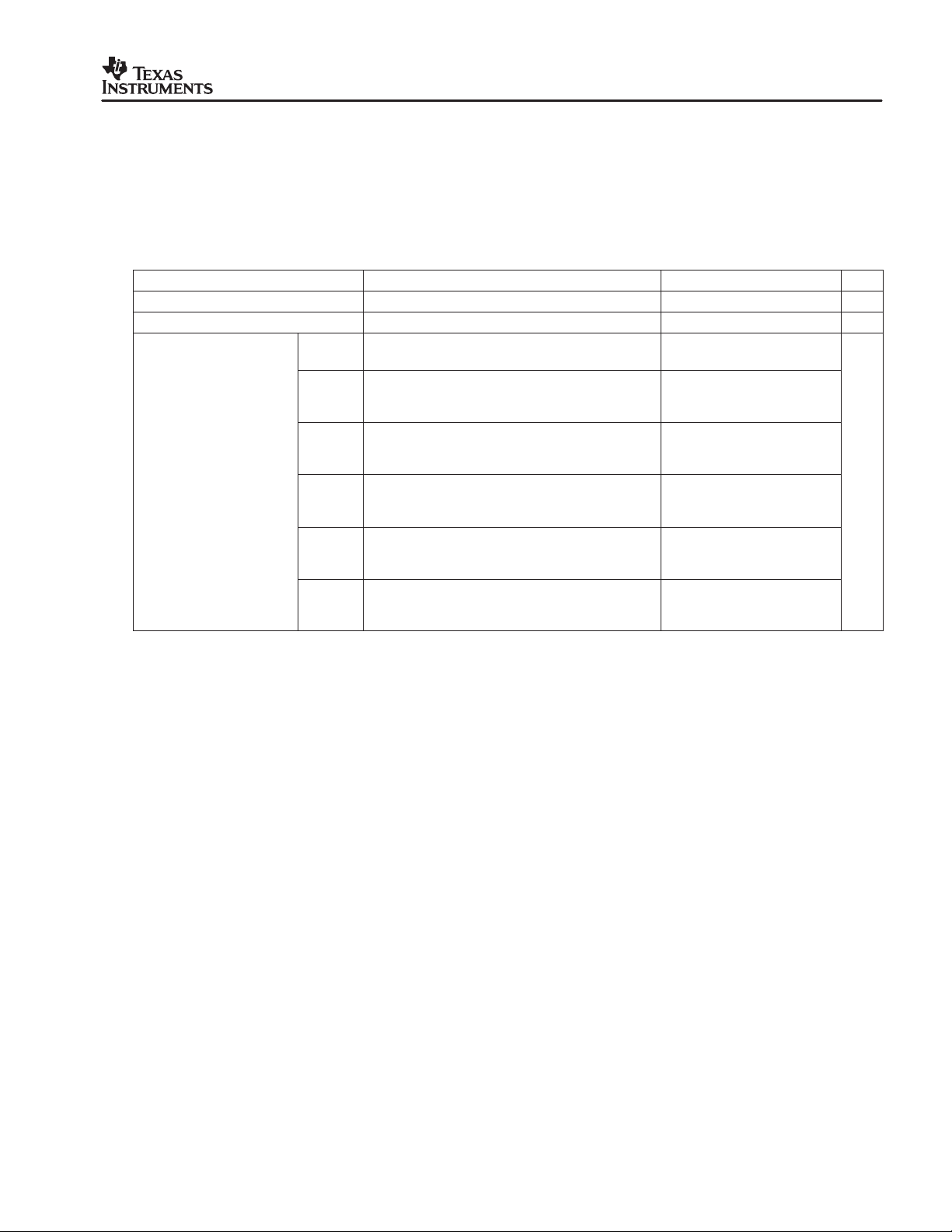
1.2 Performance Specification Summary
This section summarizes the performance specifications of the EVM. Table 1 gives the performance
specifications of the EVM. The TS pin has been disabled, for easier charging evaluation, by fixing its voltage
to a set value. See EVM schematic and data sheet for information on how to change R10 and R11 values to
use with an external thermistor
SPECIFICATION
Input DC voltage, V
Battery charge current
Power dissipation
I(DC)
(1)
, I
O(CHG)
2 Test Summary
Table 1. Performance Specification Summary
TEST CONDITIONS MIN TYP MAX UNIT
bq24100
(1 cell)
bq24103
bq24113
(1 cell)
bq24103
bq24113
(2 cell)
bq24105
bq24115
(1 cell)
bq24105
bq24115
(2 cell)
bq24105
bq24115
(3 cell)
5 V ≤ VIN ≤ 16 V, V
5 V ≤ VIN ≤ 16 V, V
9 V ≤ VIN ≤ 16 V, V
5 V ≤ VIN ≤ 16 V, V
9 V ≤ VIN ≤ 16 V, V
13.5 V ≤ VIN ≤ 16 V, V
(BAT)
(BAT)
(BAT)
(BAT)
(BAT)
(BAT)
= 4.2 V, I
= 4.2 V, I
= 8.4 V, I
= 4.2 V, I
= 8.4 V, I
= 12.6 V , I
= 1.33 A 0.6
OUT
= 1.33 A 0.6
OUT
= 1.33 A 0.85
OUT
= 1.33 A 0.6
OUT
= 1.33 A 0.85
OUT
= 1.33 A 1.17
OUT
(1)
V
+ 0.6 5.0 16 V
REG
1.33 2.0
(1)
A
W
This chapter covers the test setups and tests performed, in evaluating the EVM.
2.1 Equipment
D
Power Source: Current limited 15-V lab supply with its current limit set to 25% above the programmed
charging current (1.7 A for setup from factory). This is basically a safety limit. The actual DC input current
should be less than the charging current.
D Two Fluke 75: (optional) To measure input and output voltage and drop across current sense resistor.
2.2 Setup
The bq241xx EVM board requires a regulated supply approximately 0.3 V minimum above the regulated voltage
of the battery pack (1-cell pack: 4.2 V; 2-cell pack: 8.4 V; 3-cell pack: 12.6 V) to a maximum input voltage of
16 V
A one- to three-cell battery pack is needed for EVM evaluation. The EVM should be chosen and set up to charge
the same numbers of cells as the battery pack to be evaluated. See Table 2.
Setup the EVM as shown in Table 2. Preset the input supply to the desired voltage, turn off supply and then
connect supply to J1. Set the supply’s current limit 25% above the programmed charging current. The test setup
connections and jumper setting selections are configured for a stand-alone evaluation but can be changed to
interface with external hardware such as a microcontroller. Refer to schematic and data sheet for additional
functional information on other optional connections.
DC
.
Using the bq241xx (bqSWITCHERE)
5
Page 6
SLUU200 − July 2004
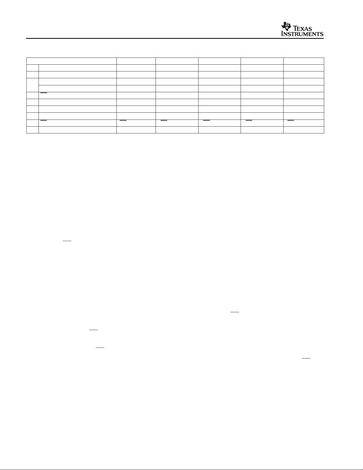
J2
Table 2. I/O and Jumper Connections (Factory Jumper Selections are shown in BOLD):
ASSEMBLY −001 −002 −003 −004 −005
U1 Device bq24100 bq24105
J1 DC+/DC−:Input voltage range (V) 5 to 16 V
BAT+/BAT−No. cell in series 1 1 1 1 1
Output regulation voltage (V) 4.2 4.2
J5 PG LED or EXT LED or EXT LED or EXT LED or EXT LED or EXT
J6 STAT1 LED or EXT LED or EXT LED or EXT LED or EXT LED or EXT
J7 STAT2 LED or EXT LED or EXT N/C no jumper N/C no jumper LED or EXT
J8 TTC or CMOD TTC no jumper TTC no jumper CMOD jumper HI CMOD jumper HI TTC no jumper
J9 CE CE jumper LO CE jumper LO CE jumper LO CE jumper LO CE jumper LO
J10 Cells or FB No jumper No jumper Cells jumper LO No jumper Cells jumper low
(1)
R5 and R7 can be changed to regulate output between approximately 3.2 V to 15.5 V. Adjust the input voltage as required. Output set to operate
at 4.2 VDC from the factory.
(2)
To operate as a two cell version (8.4V), replace battery with a two-series cell pack, set J10 to High and adjust the Input voltage between
9.2 V to 16 V.
REG
(1)
+0.8 t o 1 6
(1)
(1)
bq24113
(2)
5 to 16 V
(2)
4.2
bq24115
REG
(1)
+0.8 t o 1 6
(1)
4.2
(1)
bq24103
5 to 16
(2)
4.2
(2)
(2)
2.3 Test Procedure
Setup the evaluation board as described above, by making the necessary I/O connections and jumper
selections. Prior to test and evaluation, it is important to verify that the EVM selected is setup correctly
for the battery pack to be charged (several evaluation modules have a CELLs option that can be
programmed for two different size − number of series cells). It is highly recommended that the battery
pack to be charged has internal proteciton as a safety backup.
1. Turn on the power supply, preset to the suggested value in Table 2, and approximately 1.7 A for the current
limit setting.
2. The PG
3. The bq241xx enters pre-conditioning mode if the battery is below the V
bq241xx pre−charges the battery with a low current programmed by the ISET2 pin. If the R
resistors are the same value then the precharge is one tenth the fast charge current (I
= 133 mA) until the battery voltage reaches the V
LED should turn on along with STAT1, if the battery is charging.
(LOWV)
(LOWV)
threshold or until the precharge timer expires. If
threshold. In this mode, the
SET1
PRE−CHG
the timer expires then the charge current is terminated and the bq241xx enters fault mode. STAT1 and
STAT2 (if available) LEDs turns off when in fault mode. Note that there are several non-charging modes that
share this status state. Toggling input power or battery replacement resets fault mode.
4. Once the battery voltage is above the V
(LOWV)
is programmed for approximately 1.3 A of fast charging current. The PG
threshold, the battery enters fast charge mode. This EVM
and STAT1 LEDs should be on.
5. Once the battery reaches voltage regulation (4.2 V) the current tapers down as the battery reaches its full
capacity. The PG
6. When the current reaches the taper termination threshold, set by the R
terminated. The PG
and STAT1 LEDs should be on.
resistor, the charge is
SET2
LED should still be on and the STAT1 LED should turn off and STAT2 LED turn on.
7. If the battery discharges down to the recharge threshold, the charger starts fast charging. The PG
should still be on and the STAT2 LED should turn off and STAT1 LED turn on.
An alternative method of testing the EVM is with a source meter, that can sink or source current. This can easily
be adjusted to test each mode, in place of a battery.
3 Schematic
and R
SET2
= 1.33 A/10
LED
Figure 1 shows the schematic diagram for the EVM.
6
Using the bq241xx (bqSWITCHERE)
Page 7

SLUU200 − July 2004
Figure 1. bq241xxEVM Top Layer
Using the bq241xx (bqSWITCHERE)
7
Page 8
SLUU200 − July 2004
4 Physical Layouts
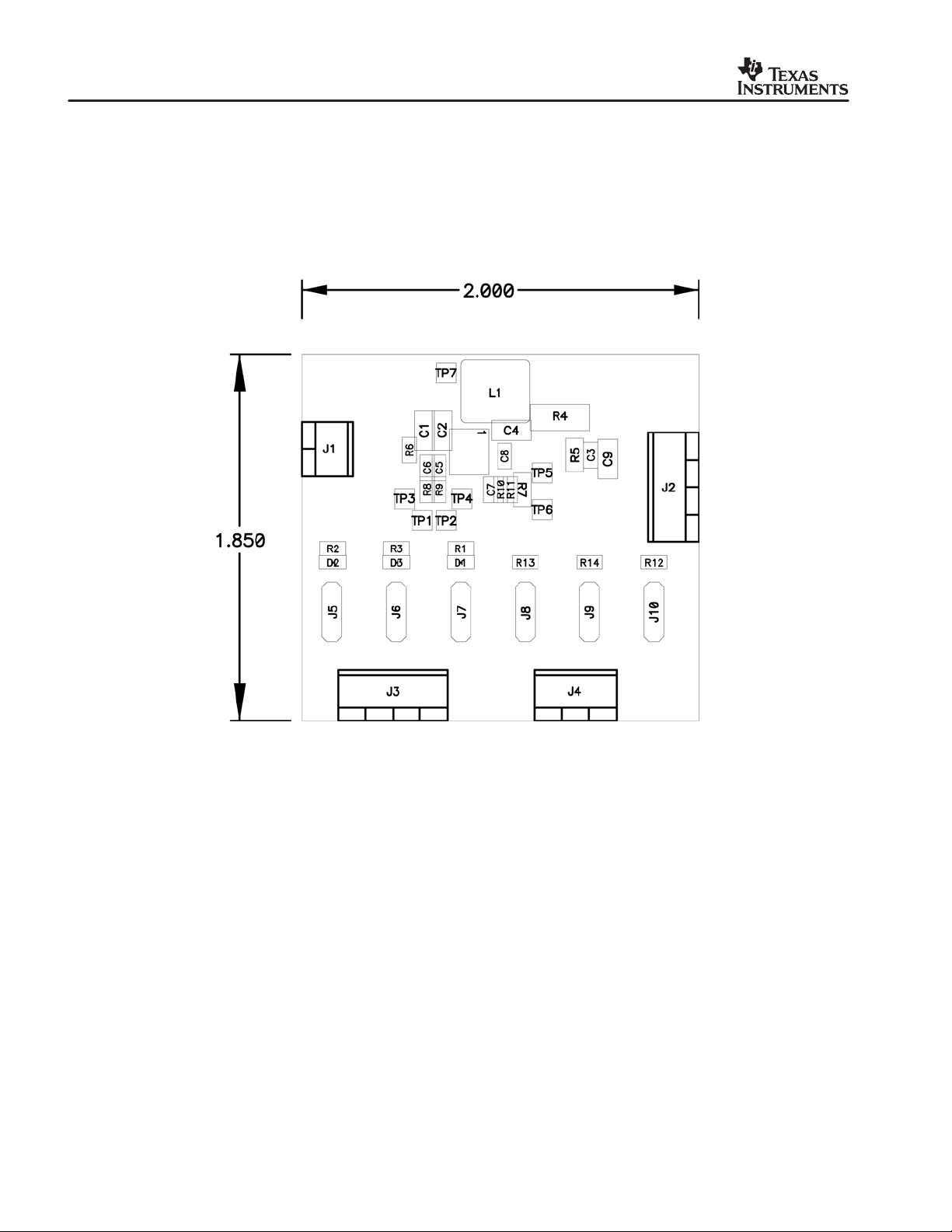
This chapter contains the board layout and assembly drawings for the EVM.
4.1 Board Layout
Figure 2 shows the top assembly of the EVM. Figure 3 shows the top silk screen. The bq24103 may also be
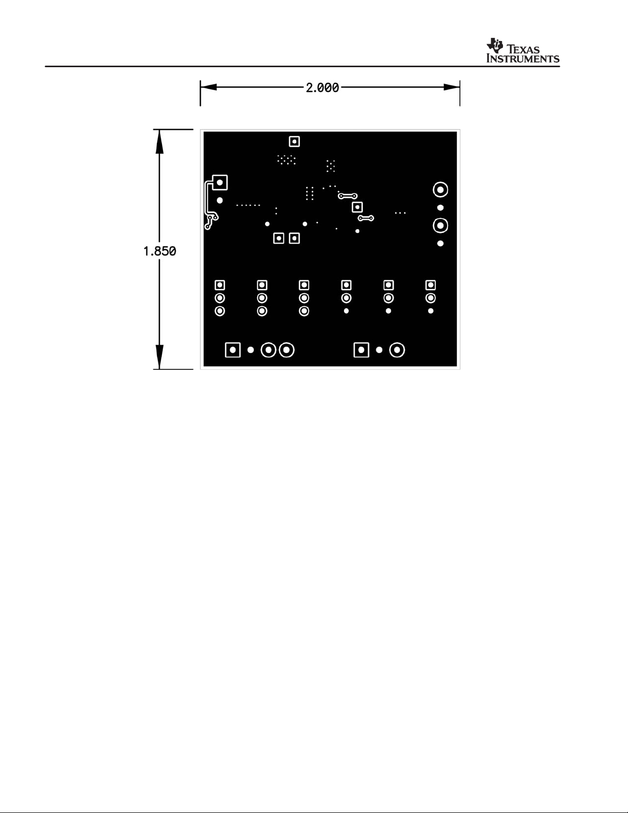
evaluated on this evaluation board. Figure 4 shows the top layer. Figure 5 shows the bottom layer view.
Figure 2. bq241xxEVM Top Assembly
8
Using the bq241xx (bqSWITCHERE)
Page 9

SLUU200 − July 2004
Figure 3. bq241xxEVM Top Silk Screen
Figure 4. bq241xx Top Layer
Using the bq241xx (bqSWITCHERE)
9
Page 10
SLUU200 − July 2004
Figure 5. bq241xxEVM Top Asembly
10
Using the bq241xx (bqSWITCHERE)
Page 11

SLUU200 − July 2004
5 List of Materials
Tables 3 through 7 list the components used in this design. With minor component adjustments this design could
be modified to meet a wide range of applications.
Table 3. bq24100EVM−001 List of Materials
REFERENCE
DESIGNATOR
C1, C2, C4 3 Capacitor, ceramic, 10 µF, 25 V, X5R, 20% 1206 Panasonic ECJ−3YB1E106M
C9 0 Capacitor, ceramic, 10 µF, 25 V, X5R, 20% 1206 Panasonic ECJ−3YB1E106M
C3 0 Capacitor, ceramic, 0.1 µF, 16 V, X7R, 10% 603 Panasonic ECJ−1VB1C104K
C5, C7, C8 3 Capacitor, ceramic, 0.1 µF, 16 V, X7R, 10% 603 Panasonic ECJ−1VB1C104K
C6 1 Capacitor, ceramic, 0.1 µF, 16 V, X7R, 10% 603 Panasonic ECJ−1VB1C104K
D1 1 Diode, LED, green, 2.1 V, 20 mA, 6 mcd 603 Liteon 160−1183−1−ND
D2 1 Diode, LED, green, 2.1 V, 20 mA, 6 mcd 603 Liteon 160−1183−1−ND
D3 1 Diode, LED, red, 1.8 V, 20 mA, 20 mcd 603 Liteon 160−1181−1−ND
J1 1 Terminal block, 2-pin, 6 A, 3.5 mm 75525 OST ED1514
J2, J3 2 Terminal block, 4-pin, 6 A, 3.5 mm 0.55 × 0.25 OST ED1516
J4 1 Terminal block, 3-pin, 6 A, 3.5 mm 0.41 × 0.25 OST ED1515
J5, J6, J8, J9 4 Header, 3−pin, 100 mil spacing, (36-pin strip) 34100 Sullins PTC36SAAN
J7 1 Header, 3−pin, 100 mil spacing, (36-pin strip) 34100 Sullins PTC36SAAN
J10 0 Header, 3−pin, 100 mil spacing, (36-pin strip) 34100 Sullins PTC36SAAN
5 Shunt, 100 mil, black 0.100 3M 929950−00
L1 1 Inductor, SMT, 10 µH, 1.84 A, 49 mΩ 0.315 × 0.287 Sumida CDRH74−100
R1 1 Resistor, chip, 1.5 kΩ, 1/16−W, 1% 603 Vishay CRCW0603−1501−F
R10 1 Resistor, chip, 4.99 kΩ, 1/16−W, 1% 603 Vishay CRCW0603−4991−F
R11, R13, R14 3 Resistor, chip, 10 kΩ, 1/16−W, 1% 603 Vishay CRCW0603−1002−F
R12 0 Resistor, chip, 0 Ω, 1/16−W, 1% 603 Vishay CRCW0603−0000−F
R2, R3 2 Resistor, chip, 1.5 kΩ, 1/16−W, 1% 603 Vishay CRCW0603−1501−F
R4 1 Resistor, chip, 0.1 Ω, ½ W, 1% 2010 Vishay CRCW1210−0R10F
R5, R7 0 Resistor, chip, 200 kΩ, 1/8−W, 1% 805 Vishay CRCW0805−2003−F
R6 1 Resistor, chip, 0 Ω, 1/16−W, 1% 603 Vishay CRCW0603−00R0−F
R8, R9 2 Resistor, chip, 7.5 kΩ, 1/16−W, 1% 603 Vishay CRCW0603−7501−F
U1 1 IC, advanced Li-Ion and Li-Pol charge management RHL−20 TI bq24100RHL
−− 1 PCB, 2.0 In x 1.9 In x .031 In Any HPA040
(1)
These assemblies are ESD sensitive, ESD precautions shall be observed.
(2)
These assemblies must be clean and free from flux and all contaminants. Use of no clean flux is not acceptable.
(3)
These assemblies must comply with workmanship standards IPC−A−610 Class 2.
(4)
C9 can be installed by the customer if using long cables (inductive load)
(5)
Place shunts as follows (Jumper pin orientation: pin 1: top (toward RD), pin 2: center, pin 3−bottom). Place shunts on J5, J6, J7−1/2 (LED);
J9−2/3 (LOW); J8−2 (optional)
QTY DESCRIPTION SIZE MFR PART NUMBER
Using the bq241xx (bqSWITCHERE)
11
Page 12

SLUU200 − July 2004
Table 4. bq24105EVM−002 List of Materials
REFERENCE
DESIGNATOR
C1, C2, C4 3 Capacitor, ceramic, 10 µF, 25 V, X5R, 20% 1206 Panasonic ECJ−3YB1E106M
C9 0 Capacitor, ceramic, 10 µF, 25 V, X5R, 20% 1206 Panasonic ECJ−3YB1E106M
C3 1 Capacitor, ceramic, 0.1 µF, 16 V, X7R, 10% 603 Panasonic ECJ−1VB1C104K
C5, C7, C8 3 Capacitor, ceramic, 0.1 µF, 16 V, X7R, 10% 603 Panasonic ECJ−1VB1C104K
C6 1 Capacitor, ceramic, 0.1 µF, 16 V, X7R, 10% 603 Panasonic ECJ−1VB1C104K
D1 1 Diode, LED, green, 2.1 V, 20 mA, 6 mcd 603 Liteon 160−1183−1−ND
D2 1 Diode, LED, green, 2.1 V, 20 mA, 6 mcd 603 Liteon 160−1183−1−ND
D3 1 Diode, LED, red, 1.8 V, 20 mA, 20 mcd 603 Liteon 160−1181−1−ND
J1 1 Terminal block, 2-pin, 6 A, 3.5 mm 75525 OST ED1514
J2, J3 2 Terminal block, 4-pin, 6 A, 3.5 mm 0.55 × 0.25 OST ED1516
J4 1 Terminal block, 3-pin, 6 A, 3.5 mm 0.41 × 0.25 OST ED1515
J5, J6, J8, J9 4 Header, 3−pin, 100 mil spacing, (36-pin strip) 34100 Sullins PTC36SAAN
J7 1 Header, 3−pin, 100 mil spacing, (36-pin strip) 34100 Sullins PTC36SAAN
J10 0 Header, 3−pin, 100 mil spacing, (36-pin strip) 34100 Sullins PTC36SAAN
5 Shunt, 100 mil, black 0.100 3M 929950−00
L1 1 Inductor, SMT, 10 µH, 1.84 A, 49 mΩ 0.315 × 0.287 Sumida CDRH74−100
R1 1 Resistor, chip, 1.5 kΩ, 1/16−W, 1% 603 Vishay CRCW0603−1501−F
R10 1 Resistor, chip, 4.99 kΩ, 1/16−W, 1% 603 Vishay CRCW0603−4991−F
R11, R13, R14 3 Resistor, chip, 10 kΩ, 1/16−W, 1% 603 Vishay CRCW0603−1002−F
R12 0 Resistor, chip, 0 Ω, 1/16−W, 1% 603 Vishay CRCW0603−0000−F
R2, R3 2 Resistor, chip, 1.5 kΩ, 1/16−W, 1% 603 Vishay CRCW0603−1501−F
R4 1 Resistor, chip, 0.1 Ω, ½ W, 1% 2010 Vishay CRCW1210−0R10F
R5, R7 2 Resistor, chip, 200 kΩ, 1/8−W, 1% 805 Vishay CRCW0805−2003−F
R6 1 Resistor, chip, 0 Ω, 1/16−W, 1% 603 Vishay CRCW0603−00R0−F
R8, R9 2 Resistor, chip, 7.5 kΩ, 1/16−W, 1% 603 Vishay CRCW0603−7501−F
U1 1 IC, Advanced Li −Ion and Li−Pol Charge Management RHL−20 TI bq24105RHL
−− 1 PCB, 2.0 In × 1.9 In × 0.031 In Any HPA040
(1)
These assemblies are ESD sensitive, ESD precautions shall be observed.
(2)
These assemblies must be clean and free from flux and all contaminants. Use of no clean flux is not acceptable.
(3)
These assemblies must comply with workmanship standards IPC−A−610 Class 2.
(4)
C9 can be installed by the customer if using long cables (inductive load)
(5)
Place shunts as follows (Jumper pin orientation: pin 1: top (toward RD), pin 2: center, pin 3−bottom). Place shunts on J5, J6, J7−1/2 (LED);
J9−2/3 (LOW); J8−2 (optional)
QTY DESCRIPTION SIZE MFR PART NUMBER
12
Using the bq241xx (bqSWITCHERE)
Page 13

Table 5. bq24113EVM−003 List of Materials
SLUU200 − July 2004
REFERENCE
DESIGNATOR
C1, C2, C4 3 Capacitor, ceramic, 10 µF, 25 V, X5R, 20% 1206 Panasonic ECJ−3YB1E106M
C9 0 Capacitor, ceramic, 10 µF, 25 V, X5R, 20% 1206 Panasonic ECJ−3YB1E106M
C3 0 Capacitor, ceramic, 0.1 µF, 16 V, X7R, 10% 603 Panasonic ECJ−1VB1C104K
C5, C7, C8 3 Capacitor, ceramic, 0.1 µF, 16 V, X7R, 10% 603 Panasonic ECJ−1VB1C104K
C6 0 Capacitor, ceramic, 0.1 µF, 16 V, X7R, 10% 603 Panasonic ECJ−1VB1C104K
D1 0 Diode, LED, green, 2.1 V, 20 mA, 6 mcd 603 Liteon 160−1183−1−ND
D2 1 Diode, LED, green, 2.1 V, 20 mA, 6 mcd 603 Liteon 160−1183−1−ND
D3 1 Diode, LED, red, 1.8 V, 20 mA, 20 mcd 603 Liteon 160−1181−1−ND
J1 1 Terminal block, 2-pin, 6 A, 3.5 mm 75525 OST ED1514
J2, J3 2 Terminal block, 4-pin, 6 A, 3.5 mm 0.55 × 0.25 OST ED1516
J4 1 Terminal block, 3-pin, 6 A, 3.5 mm 0.41 × 0.25 OST ED1515
J5, J6, J8, J9 4 Header, 3−pin, 100 mil spacing, (36-pin strip) 34100 Sullins PTC36SAAN
J7 0 Header, 3−pin, 100 mil spacing, (36-pin strip) 34100 Sullins PTC36SAAN
J10 1 Header, 3−pin, 100 mil spacing, (36-pin strip) 34100 Sullins PTC36SAAN
5 Shunt, 100 mil, black 0.100 3M 929950−00
L1 1 Inductor, SMT, 10 µH, 1.84 A, 49 mΩ 0.315 × 0.287 Sumida CDRH74−100
R1 0 Resistor, chip, 1.5 kΩ, 1/16−W, 1% 603 Vishay CRCW0603−1501−F
R10 1 Resistor, chip, 4.99 kΩ, 1/16−W, 1% 603 Vishay CRCW0603−4991−F
R11, R13, R14 3 Resistor, chip, 10 kΩ, 1/16−W, 1% 603 Vishay CRCW0603−1002−F
R12 1 Resistor, chip, 0 Ω, 1/16−W, 1% 603 Vishay CRCW0603−0000−F
R2, R3 2 Resistor, chip, 1.5 kΩ, 1/16−W, 1% 603 Vishay CRCW0603−1501−F
R4 1 Resistor, chip, 0.1 Ω, ½ W, 1% 2010 Vishay CRCW1210−0R10F
R5, R7 0 Resistor, chip, 200 kΩ, 1/8−W, 1% 805 Vishay CRCW0805−2003−F
R6 1 Resistor, chip, 0 Ω, 1/16−W, 1% 603 Vishay CRCW0603−00R0−F
R8, R9 2 Resistor, chip, 7.5 kΩ, 1/16−W, 1% 603 Vishay CRCW0603−7501−F
U1 1 IC, Advanced Li-Ion and Li-Pol Charge Management RHL−20 TI bq24113RHL
−− 1 PCB, 2.0 In × 1.9 In × 0.031 In Any HPA040
(1)
These assemblies are ESD sensitive, ESD precautions shall be observed.
(2)
These assemblies must be clean and free from flux and all contaminants. Use of no clean flux is not acceptable.
(3)
These assemblies must comply with workmanship standards IPC−A−610 Class 2.
(4)
C9 can be installed by the customer if using long cables (inductive load)
(5)
Place shunts as follows (Jumper pin orientation: pin 1: top (toward RD), pin 2: center, pin 3−bottom). Place shunts on J8−1/2 (Hi), J5 & J6−1/2
(LED), J9−2/3 (LOW). Place shunts on J10−2/3 (LOW)
QTY DESCRIPTION SIZE MFR PART NUMBER
Using the bq241xx (bqSWITCHERE)
13
Page 14

SLUU200 − July 2004
Table 6. bq24115EVM−004 List of Materials
REFERENCE
DESIGNATOR
C1, C2, C4 3 Capacitor, ceramic, 10 µF, 25 V, X5R, 20% 1206 Panasonic ECJ−3YB1E106M
C9 0 Capacitor, ceramic, 10 µF, 25 V, X5R, 20% 1206 Panasonic ECJ−3YB1E106M
C3 1 Capacitor, ceramic, 0.1 µF, 16 V, X7R, 10% 603 Panasonic ECJ−1VB1C104K
C5, C7, C8 3 Capacitor, ceramic, 0.1 µF, 16 V, X7R, 10% 603 Panasonic ECJ−1VB1C104K
C6 0 Capacitor, ceramic, 0.1 µF, 16 V, X7R, 10% 603 Panasonic ECJ−1VB1C104K
D1 0 Diode, LED, green, 2.1 V, 20 mA, 6 mcd 603 Liteon 160−1183−1−ND
D2 1 Diode, LED, green, 2.1 V, 20 mA, 6 mcd 603 Liteon 160−1183−1−ND
D3 1 Diode, LED, red, 1.8 V, 20 mA, 20 mcd 603 Liteon 160−1181−1−ND
J1 1 Terminal block, 2-pin, 6 A, 3.5 mm 75525 OST ED1514
J2, J3 2 Terminal block, 4-pin, 6 A, 3.5 mm 0.55 × 0.25 OST ED1516
J4 1 Terminal block, 3-pin, 6 A, 3.5 mm 0.41 × 0.25 OST ED1515
J5, J6, J8, J9 4 Header, 3−pin, 100 mil spacing, (36-pin strip) 34100 Sullins PTC36SAAN
J7 0 Header, 3−pin, 100 mil spacing, (36-pin strip) 34100 Sullins PTC36SAAN
J10 0 Header, 3−pin, 100 mil spacing, (36-pin strip) 34100 Sullins PTC36SAAN
4 Shunt, 100 mil, black 0.100 3M 929950−00
L1 1 Inductor, SMT, 10 µH, 1.84 A, 49 mΩ 0.315 × 0.287 Sumida CDRH74−100
R1 0 Resistor, chip, 1.5 kΩ, 1/16−W, 1% 603 Vishay CRCW0603−1501−F
R10 1 Resistor, chip, 4.99 kΩ, 1/16−W, 1% 603 Vishay CRCW0603−4991−F
R11, R13, R14 3 Resistor, chip, 10 kΩ, 1/16−W, 1% 603 Vishay CRCW0603−1002−F
R12 0 Resistor, chip, 0 Ω, 1/16−W, 1% 603 Vishay CRCW0603−0000−F
R2, R3 2 Resistor, chip, 1.5 kΩ, 1/16−W, 1% 603 Vishay CRCW0603−1501−F
R4 1 Resistor, chip, 0.1 Ω, ½ W, 1% 2010 Vishay CRCW1210−0R10F
R5, R7 2 Resistor, chip, 200 kΩ, 1/8−W, 1% 805 Vishay CRCW0805−2003−F
R6 1 Resistor, chip, 0 Ω, 1/16−W, 1% 603 Vishay CRCW0603−00R0−F
R8, R9 2 Resistor, chip, 7.5 kΩ, 1/16−W, 1% 603 Vishay CRCW0603−7501−F
U1 1 IC, Advanced Li-Ion and Li-Pol Charge Management RHL−20 TI bq24115RHL
−− 1 PCB, 2.0 In × 1.9 In × 0.031 In Any HPA040
(1)
These assemblies are ESD sensitive, ESD precautions shall be observed.
(2)
These assemblies must be clean and free from flux and all contaminants. Use of no clean flux is not acceptable.
(3)
These assemblies must comply with workmanship standards IPC−A−610 Class 2.
(4)
C9 can be installed by the customer if using long cables (inductive load)
(5)
Place shunts as follows (Jumper pin orientation: pin 1: top (toward RD), pin 2: center, pin 3−bottom). Place shunts on J8−1/2 (Hi), J5 & J6−1/2
(LED), J9−2/3 (LOW)
QTY DESCRIPTION SIZE MFR PART NUMBER
14
Using the bq241xx (bqSWITCHERE)
Page 15

Table 7. bq24103EVM−005 List of Materials
SLUU200 − July 2004
REFERENCE
DESIGNATOR
C1, C2, C4 3 Capacitor, ceramic, 10 µF, 25 V, X5R, 20% 1206 Panasonic ECJ−3YB1E106M
C9 0 Capacitor, ceramic, 10 µF, 25 V, X5R, 20% 1206 Panasonic ECJ−3YB1E106M
C3 0 Capacitor, ceramic, 0.1 µF, 16 V, X7R, 10% 603 Panasonic ECJ−1VB1C104K
C5, C7, C8 3 Capacitor, ceramic, 0.1 µF, 16 V, X7R, 10% 603 Panasonic ECJ−1VB1C104K
C6 1 Capacitor, ceramic, 0.1 µF, 16 V, X7R, 10% 603 Panasonic ECJ−1VB1C104K
D1 1 Diode, LED, green, 2.1 V, 20 mA, 6 mcd 603 Liteon 160−1183−1−ND
D2 1 Diode, LED, green, 2.1 V, 20 mA, 6 mcd 603 Liteon 160−1183−1−ND
D3 1 Diode, LED, red, 1.8 V, 20 mA, 20 mcd 603 Liteon 160−1181−1−ND
J1 1 Terminal block, 2-pin, 6 A, 3.5 mm 75525 OST ED1514
J2, J3 2 Terminal block, 4-pin, 6 A, 3.5 mm 0.55 × 0.25 OST ED1516
J4 1 Terminal block, 3-pin, 6 A, 3.5 mm 0.41 × 0.25 OST ED1515
J5, J6, J8, J9 4 Header, 3−pin, 100 mil spacing, (36-pin strip) 34100 Sullins PTC36SAAN
J7 1 Header, 3−pin, 100 mil spacing, (36-pin strip) 34100 Sullins PTC36SAAN
J10 1 Header, 3−pin, 100 mil spacing, (36-pin strip) 34100 Sullins PTC36SAAN
6 Shunt, 100 mil, black 0.100 3M 929950−00
L1 1 Inductor, SMT, 10 µH, 1.84 A, 49 mΩ 0.315 × 0.287 Sumida CDRH74−100
R1 1 Resistor, chip, 1.5 kΩ, 1/16−W, 1% 603 Vishay CRCW0603−1501−F
R10 1 Resistor, chip, 4.99 kΩ, 1/16−W, 1% 603 Vishay CRCW0603−4991−F
R11, R13, R14 3 Resistor, chip, 10 kΩ, 1/16−W, 1% 603 Vishay CRCW0603−1002−F
R12 1 Resistor, chip, 0 Ω, 1/16−W, 1% 603 Vishay CRCW0603−0000−F
R2, R3 2 Resistor, chip, 1.5 kΩ, 1/16−W, 1% 603 Vishay CRCW0603−1501−F
R4 1 Resistor, chip, 0.1 Ω, ½ W, 1% 2010 Vishay CRCW1210−0R10F
R5, R7 0 Resistor, chip, 200 kΩ, 1/8−W, 1% 805 Vishay CRCW0805−2003−F
R6 1 Resistor, chip, 0 Ω, 1/16−W, 1% 603 Vishay CRCW0603−00R0−F
R8, R9 2 Resistor, chip, 7.5 kΩ, 1/16−W, 1% 603 Vishay CRCW0603−7501−F
U1 1 IC, Advanced Li-Ion and Li-Pol Charge Management RHL−20 TI bq24103RHL
−− 1 PCB, 2.0 In × 1.9 In × 0.031 In Any HPA040
(1)
These assemblies are ESD sensitive, ESD precautions shall be observed.
(2)
These assemblies must be clean and free from flux and all contaminants. Use of no clean flux is not acceptable.
(3)
These assemblies must comply with workmanship standards IPC−A−610 Class 2.
(4)
C9 can be installed by the customer if using long cables (inductive load)
(5)
Place shunts as follows (Jumper pin orientation: pin 1: top (toward RD), pin 2: center, pin 3−bottom). Place shunts on J5, J6, J7−1/2 (LED);
J9−2/3 (LOW); J8−2 (optional). Place shunts on J10−2/3 (LOW)
QTY DESCRIPTION SIZE MFR PART NUMBER
6 References
1. bq241xx Synchronous Switchmode Li−Ion and Li−Pol Charge Management IC With Integrated PowerFETs
(bqSWITCHER) datasheet (SLUS606)
Using the bq241xx (bqSWITCHERE)
15
Page 16

IMPORTANT NOTICE
Texas Instruments Incorporated and its subsidiaries (TI) reserve the right to make corrections, modifications,
enhancements, improvements, and other changes to its products and services at any time and to discontinue
any product or service without notice. Customers should obtain the latest relevant information before placing
orders and should verify that such information is current and complete. All products are sold subject to TI’s terms
and conditions of sale supplied at the time of order acknowledgment.
TI warrants performance of its hardware products to the specifications applicable at the time of sale in
accordance with TI’s standard warranty. Testing and other quality control techniques are used to the extent TI
deems necessary to support this warranty . Except where mandated by government requirements, testing of all
parameters of each product is not necessarily performed.
TI assumes no liability for applications assistance or customer product design. Customers are responsible for
their products and applications using TI components. To minimize the risks associated with customer products
and applications, customers should provide adequate design and operating safeguards.
TI does not warrant or represent that any license, either express or implied, is granted under any TI patent right,
copyright, mask work right, or other TI intellectual property right relating to any combination, machine, or process
in which TI products or services are used. Information published by TI regarding third-party products or services
does not constitute a license from TI to use such products or services or a warranty or endorsement thereof.
Use of such information may require a license from a third party under the patents or other intellectual property
of the third party, or a license from TI under the patents or other intellectual property of TI.
Reproduction of information in TI data books or data sheets is permissible only if reproduction is without
alteration and is accompanied by all associated warranties, conditions, limitations, and notices. Reproduction
of this information with alteration is an unfair and deceptive business practice. TI is not responsible or liable for
such altered documentation.
Resale of TI products or services with statements different from or beyond the parameters stated by TI for that
product or service voids all express and any implied warranties for the associated TI product or service and
is an unfair and deceptive business practice. TI is not responsible or liable for any such statements.
Following are URLs where you can obtain information on other Texas Instruments products and application
solutions:
Products Applications
Amplifiers amplifier.ti.com Audio www.ti.com/audio
Data Converters dataconverter.ti.com Automotive www.ti.com/automotive
DSP dsp.ti.com Broadband www.ti.com/broadband
Interface interface.ti.com Digital Control www.ti.com/digitalcontrol
Logic logic.ti.com Military www.ti.com/military
Power Mgmt power.ti.com Optical Networking www.ti.com/opticalnetwork
Microcontrollers microcontroller.ti.com Security www.ti.com/security
Telephony www.ti.com/telephony
Video & Imaging www.ti.com/video
Wireless www.ti.com/wireless
Mailing Address: Texas Instruments
Post Office Box 655303 Dallas, Texas 75265
Copyright 2004, Texas Instruments Incorporated
 Loading...