

查询BQ2058SN-C5供应商
bq2058
Lithium Ion Pack Supervisor
for 3- and 4-Cell Packs
Features
Protects and individually moni
➤
tors three or four Li-Ion series
cells for overvoltage, undervolt
age
Monitors pack for overcurrent
➤
Designed for battery pack inte
➤
gration
Minimal external components
➤
Drives external FET switches
➤
Selectable overvoltage (V
➤
thresholds
Mask-programmable by
-
Unitrode
- Standard version–4.25V
➤ Supply current: 25µA typical
➤ Sleep current: 0.7µA typical
➤ 16-pin 150-mil narrow SOIC
General Description
The bq2058 Lithium Ion Pack Super
visor is designed to control the charge
and discharge cell voltages for three or
four lithium ion (Li-Ion) series cells,
accommodating battery packs contain
ing series/parallel configurations. The
low operating current does not over
discharge the cells during periods of
storage and does not significantly in
crease the system discharge load. The
bq2058 can be part of a low-cost Li-Ion
charge control system within the bat
tery pack.
)
OV
The bq2058 controls two external FETs
to limit the charge and discharge potentials. The bq2058 allows charging when
each individual cell voltage is below V
(overvoltage limit). If the voltage on any
cell exceeds V
delay period (t
driven high, shutting off charge to the
battery pack. This safety feature pre-
for a user-configurable
OV
), the CHG pin is
OVD
vents overcharge of any cell within
the battery pack. After an overvolt
age condition occurs, each cell must
fall below V
for the bq2058 to re-enable charging.
(charge enable voltage)
CE
The bq2058 protects batteries from
-
overdischarge. If the voltage on any
cell falls below V
-
limit) for a user-configurable delay pe
riod (t
-
high, shutting off the battery dis
), the DSG output is driven
UVD
(undervoltage
UV
charge. This safety feature prevents
overdischarge of any cell within the
-
battery pack.
The bq2058 also stops discharge on
detection of an overcurrent condition,
such as a short circuit. If an overcurrent condition occurs for a userconfigurable delay period (t
OV
DSG
output is driven high, disconnecting the load from the pack. DSG
mains high until removal of the short
circuit or overcurrent condition.
OCD
-
-
-
), the
re-
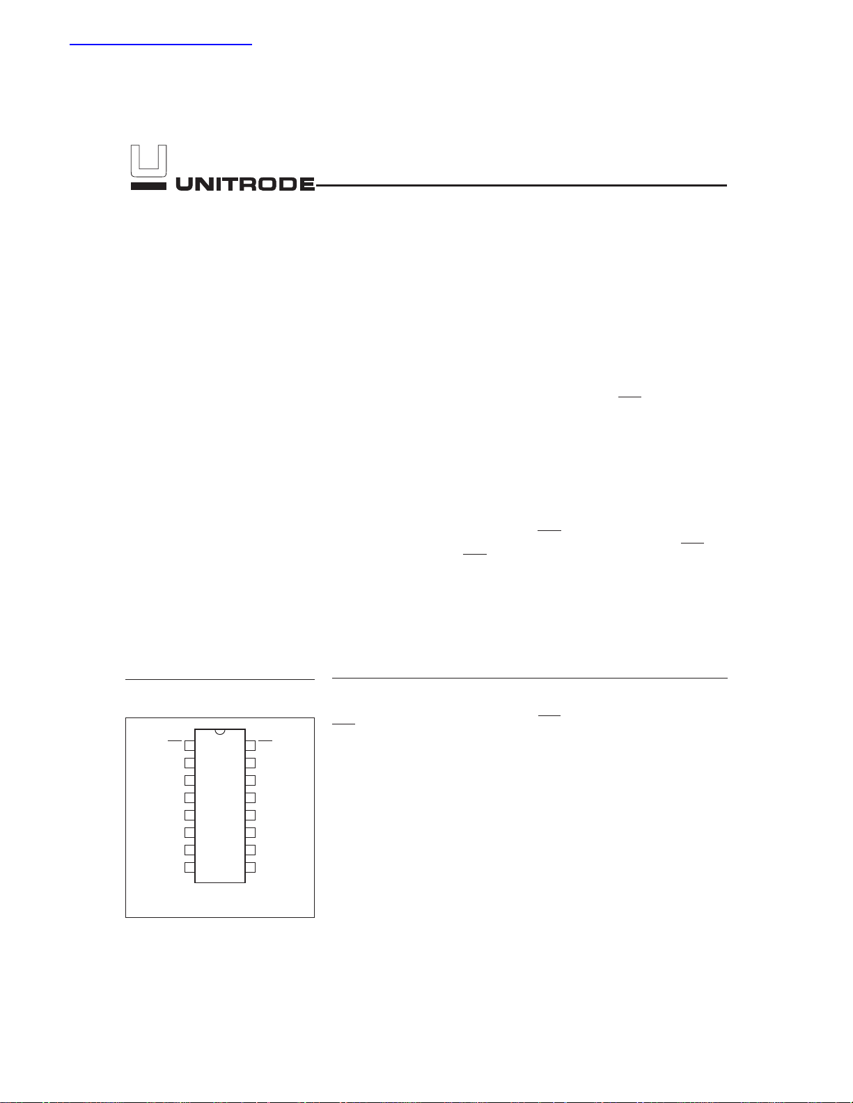
Pin Connections
16
1
2
15
3
14
4
13
5
12
6
11
7
10
8
9
1/99 I
BAT
BAT
BAT
BAT
CHG
CTL
V
CSL
SS
4N
3N
2N
1N
16-Pin Narrow SOIC
DSG
NSEL
UVD
OVD
OCD
V
CC
CSH
BAT
PN205801.eps
Pin Names
CHG Charge control output
CTL Pack disable input
V
SS
Low potential input
CSL Current sense low-side
input
BAT
BAT
1P
BAT
BAT
Battery 4 negative input
4N
Battery 3 negative input
3N
Battery 2 negative input
2N
Battery 1 negative input
1N
1
DSG Discharge control output
NSEL 3- or 4-cell selection
UVD Undervoltage delay input
OVD Overvoltage delay input
OCD Overcurrent delay input
V
CC
High potential input
CSH Current sense high-side
input
BAT
Battery 1 positive input
1P
bq2058
Pin Descriptions
CHG Charge control output
This push-pull output controls the charge
path to the battery pack. Charging is al
lowed when low.
CTL Pack disable input
When high, this input allows an external
source to disable the pack by making both
DSG
and CHG inactive. For normal opera
tion, the CTL pin is low.
V
SS
CSL Overcurrent sense low-side input
BAT
BAT
BAT
BAT
Low potential input
This input is connected between the low-side
discharge FET (or sense resistor) and BAT
to enable overcurrent sensing in the battery
pack’s ground path.
Battery 4 negative input
4N
This input is connected to the negative terminal of the cell designated BAT4 in Figure 2.
Battery 3 negative input
3N
This input is connected to the negative terminal
of the cell designated BAT3 in Figure 2.
Battery 2 negative input
2N
This input is connected to the negative termi
nal of the cell designated BAT2 in Figure 2.
Battery 1 negative input
1N
This input is connected to the negative termi
nal of the cell designated BAT1 in Figure 2.
This input is connected to BAT
cell configuration.
DSG
-
Discharge control output
This push-pull output controls the discharge
path to the battery pack. Discharge is al
lowed when low.
NSEL Number of cells input
This input selects the number of series cells
-
in the pack. NSEL should connect to V
four cells and to V
for three cells.
SS
UVD Undervoltage delay input
This input uses an external capacitor to V
to set the undervoltage delay timing.
OVD Overvoltage delay input
4N
This input uses an external capacitor to V
to set the overvoltage delay timing.
OCD Overcurrent delay input
This input uses an external capacitor to V
to set the overcurrent delay timing.
V
CC
High potential input
CSH Overcurrent sense high-side input
This input is connected between the
high-side discharge FET (or sense resistor)
-
BAT
-
and BAT
the battery pack’s positive supply path.
Battery 1 positive input
1P
This input is connected to the positive terminal
of the cell designated BAT1 in Figure 2.
to enable overcurrent sense in
1P
in a three-
1P
CC
-
for
CC
CC
CC
Table 1. Pin Configuration for 3- and 4-Series Cells
Number of Cells Configuration Pins Battery Pins
BAT1N– Positive terminal of first cell
BAT
– Negative terminal of first cell
3 cells
4 cells
BAT
tied to BAT
1N
NSEL = V
NSEL = V
1P
SS
CC
2
2N
BAT
– Negative terminal of second cell
3N
BAT
– Negative terminal of third cell
4N
BAT1P– Positive terminal of first cell
BAT
– Negative terminal of first cell
1N
BAT
– Negative terminal of second cell
2N
BAT
– Negative terminal of third cell
3N
BAT
– Negative terminal of fourth cell
4N

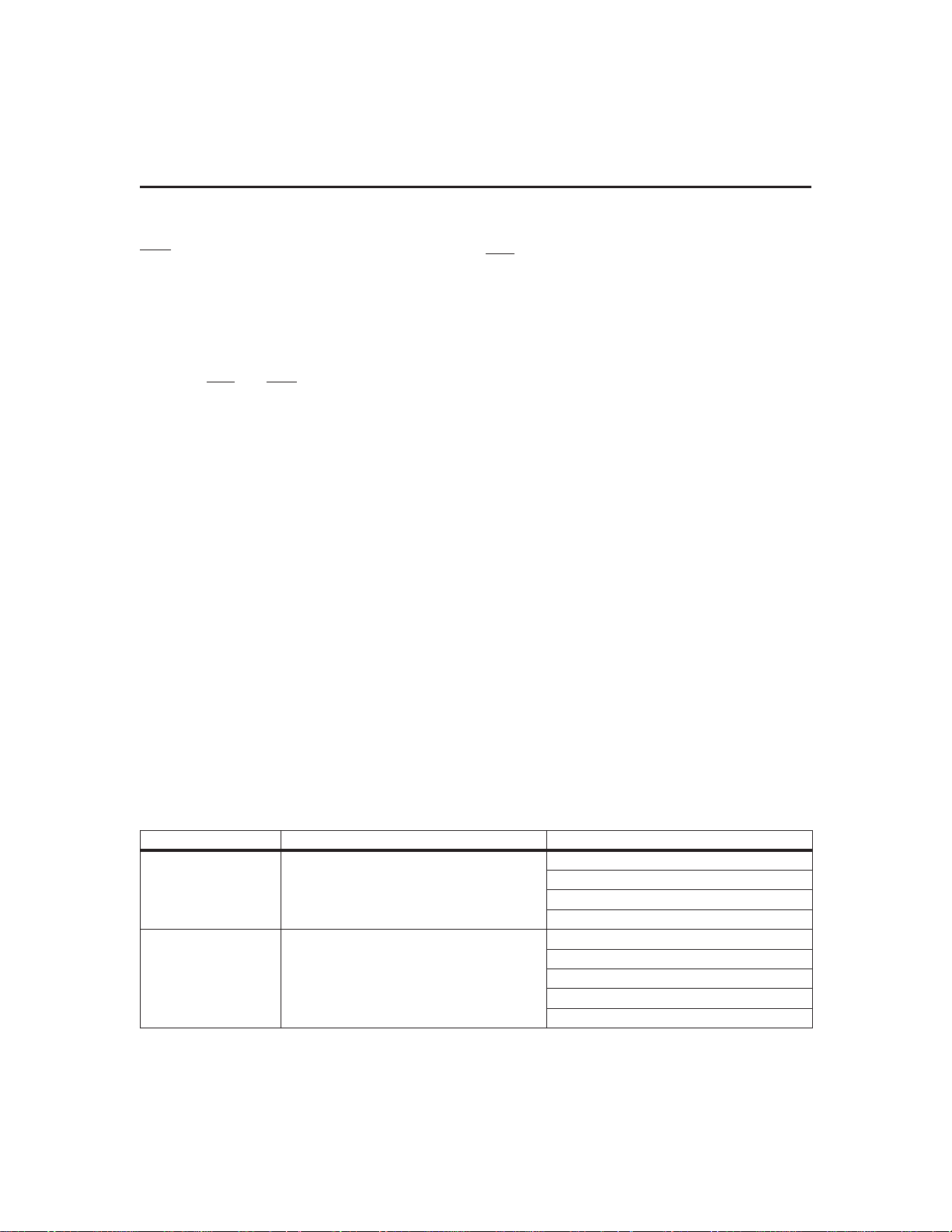
Cell Inputs
Pin 9
Pin 8
Pin 7
Pin 6
Pin 5
Pin 3
Chip Negative
Supply
B1P
B1N
B2N
B3N
B4N
V
Sel4
Sel3
Sel2
Sel1
OV
V
V
bq2058
+
-
+
Sel4
Sel3
Sel2
Sel1
Sel4
Sel3
Sel2
+
Sel1
CE
Sel4
+
Sel3
UV
Sel2
Sel1
Q
D
CK
QB
Q
D
CK
QB
Q
D
CK
QB
Q
D
CK
QB
Q
D
CK
QB
Q
D
CK
QB
Q
D
CK
QB
Q
D
CK
QB
Q
D
CK
QB
Q
D
CK
QB
Q
D
CK
QB
Q
D
CK
QB
Pin 10
Pin 9
Pin 4
Pin 5
CSH
B1P
CSL
B4N
160mV
160mV
Number of Cells Select
Pin 15
NSEL
Sleep
Any_Above_V
Any_Below_V
OV
OVD
Pin 13
Discharge Off Delay Capacitor Input
UV
Edge
Reset
Capacitor
UVD
Pin 14
Charge Off Delay Capacitor Input
Sense High-side Input
CSH
Pin 10
Pin 9
Pin 4
Pin 5
Overcurrent Delay
Capacitor Input
+
+
70mV
B1P
Sense Low-side Input
CSL
70mV
B4N
+
Pin 12
OCD
NSEL
Sleep
Clock
Sel4
Sel3
Sel2
Sel1
Edge
Non-Retrigger
Oneshot
Reset
Capacitor
All_Below_V
Out
Non-Retrigger
Oneshot
+
Edge
Reset
Out
Non-Retrigger
Oneshot
Capacitor
Pin 2
CTL
External Output Control
Out
Sel4
Sel3
Sel2
Sel1
D
CK
Reset
QB
CE
D
CK
Reset
D
CK
Reset
Sleep
Q
QB
QB
Overcharge
Pin 1
CHG
Charge Control
Output
Pin 16
DSG
Discharge Control
Output
Overcurrent
Figure 1. Block Diagram
3
bq2058
Functional Description
Figure 1 is a block diagram outlining the major compo
nents of the bq2058. Figure 2 shows a 3- or 4-cell pack
supervisor circuit. The following sections detail the vari
ous functional aspects of the bq2058.
Thresholds
The bq2058 monitors the lithium ion pack for the condi
tions listed below. Shown with these conditions are the
respective thresholds used to determine if that condition
exists:
Overvoltage (VOV)
■
Undervoltage (VUV)
■
Overcurrent (V
■
Charge Enable (VCE)
■
Charge Detect (VCD)
■
B1P
B1N
B2N
B3N
B4N
OCH,VOCL
R3
10K
R4
10K
R5
10K
R7
10K
R8
10K
Notes:
1. For automatic short circuit recovery.
2. Remove R11 for 4-cell. Remove R10 and connect
B1P to B1N for 3-cells.
0.001uF
C2
0.001uF
0.001uF
C4
0.001uF
)
* See note 2.
U1
C9
0.1uF
C1
C3
R1
2.7K
D1
BAT54
bq2058
11
VCC
9
BAT1P
8
BAT1N
7
BAT2N
6
BAT3N
5
BAT4N
3
VSS
The bq2058 samples a cell every 40ms (typical). Every
sample is a fully differential measurement of each cell.
During this sample period, the bq2058 compares the
measurements with these thresholds to determine if any
of the these conditions exist: V
-
OV,VUV
, and VCE.
Overcurrent and charge detect are conditions that are
not sampled, but are continuously monitored.
Initialization
-
On initial power-up, such as connecting the battery pack
for the first time to the bq2058, the bq2058 enters the
low-power sleep mode, disabling the DSG
output. It is
recommended that a top to bottom cell connection
be made at pack assembly for proper initializa
tion. A charging supply must be applied to the bq2058
circuit to enable the pack. See Low-Power Sleep Mode
and Charge Detect sections.
R2
6.98K
Q2
Si4435DY
100K
C8
0.1uF
C6
0.1uF
Q1
Si4435DY
R9
Q3
2N7002
1M
R6
POS
TP1
NEG
NSEL
4-Cell
OVD
UVD
OCD
DSG
CSH
CHG
CTL
CSL
R10
0 Ohm
* See note 1.
Q4
ZVP3306F
R11
0 Ohm
3-Cell
C10
0.1uF
15
C5
13
0.1uF
14
12
16
10
1
2
4
0.01uF
C7
-
Figure 2. 3- or 4-Cell Li-Ion Battery Pack Supervisor
4
bq2058
Low-Power Sleep Mode
The bq2058 enters the low-power sleep mode in two dif
ferent ways:
1. On initial power-up.
2. After the detection of an undervoltage condi
UV
.
tion–V
When the bq2058 enters the low-power sleep mode, DSG
is driven high and the device consumes 0.7µA (typical).
The bq2058 only comes out of low-power sleep mode
when a valid charge-detect condition exists.
Charge Detect
The bq2058 continuously monitors for a charge-detect con
dition. A valid charge-detect condition exists when either
of the conditions are true:
CSL < BAT
CSH > BAT
A valid charge-detect enables the DSG
- 70mV (VCD)
4N
+ 70mV (VCD)
1P
output, allowing
charging of the lithium ion cells. This is accomplished
by applying the charging supply to the pack.
Undervoltage
Undervoltage (or overdischarge) protection is asserted
when any cell voltage drops below the V
and remains below the V
exceeding a user-configurable delay (t
threshold for a time
UV
UV
). The DSG
UVD
threshold
output is driven high disabling the discharge of the
pack. The bq2058 then enters the low-power sleep
mode.
Overvoltage
Overvoltage (or overcharge) protection is asserted when
any cell voltage exceeds the V
above the V
configurable delay (t
disabling charge into the battery pack. Charging is dis
threshold for a time exceeding a user-
OV
). The CHG pin is driven high,
OVD
abled until a valid charge enable exists. See Charge En
able section.
Important note: If any battery pin floats (BAT
BAT
), the bq2058 assumes an overvoltage has
1N–4N
occurred.
Because of different manufacturers specifications for
overvoltage thresholds, the bq2058 can be available with
different V
options. Table 2 summarizes these differ
OV
ent voltage thresholds.
threshold and remains
OV
1P
Table 2. Overvoltage Threshold Options
-
bq2058 4.25V
bq2058C 4.325
bq2058D 4.30V
bq2058G* 4.375V
bq2058R 4.35V
bq2058W 3.4V
The overvoltage threshold limits are programmed
at Unitrode. The bq2058 is the standard option
-
that is more readily available for sampling and
prototyping purposes. Please contact Unitrode
for other voltage threshold and tolerance options.
Part No. VOVLimit
Charge Enable
A valid charge enable indicates that an overvoltage
(overcharge) condition no longer exists and that the
pack is ready to accept further charge. Once overvoltage
protection is asserted, charging will not be enabled until all cell voltages fall below V
a function of V
its.
and changes with different VOVlim-
OV,
V
= VOV- 150mV
CE
. The VCEthreshold is
CE
Overcurrent
The bq2058 detects an overcurrent (or short circuit) condition only in the discharge direction. Overcurrent pro
tection is asserted when either of the conditions occurs
and remain for a time exceeding a user-configurable de
lay (t
where:
-
-
,
When either of these conditions occurs, DSG
high, disconnecting the load from the pack. DSG
mains high until both of the voltage conditions are false,
indicating removal of the short-circuit condition. The
user can facilitate clearing these conditions by inserting
-
the battery pack into a charger.
The low-side overcurrent sense can be disabled by con
necting CSL to BAT
greater than BAT
high-side detection must be used with CSH.
OCD
):
CSL > BAT
CSH < BAT1P- V
V
= 160mV (low-side detect)
OCL
V
= 160mV (high-side detect)
OCH
. This ensures that CSL is never
4N
. If low-side detection is disabled,
4N
4N
+ V
OCL
OCH
is driven
re
-
-
-
-
5

bq2058
The FETs in the charge/discharge path controlled by the
CHG
and DSG pins affect the overcurrent level. The
on-resistance of these FETs need to be taken into ac
count when determining overcurrent levels.
Condition CHG pin DSG pin
Normal operation Low Low
Overvoltage High Low
Undervoltage Lo w High
Overcurrent Low High
Floating battery input High Indeterminate
CTL = high High High
CHG and DSG States
The CHG and DSG output truth table is shown below.
The polarities of CHG
and DSG are mask programmable
at Unitrode. Push-pull vs. open-drain configuration is
also mask-configurable at Unitrode. Please contact
Unitrode for availability of these variations.
Number of Cells
The user must configure the bq2058 for three- or fourseries cell operation. For a three-cell pack, NSEL
should be tied directly to V
N
should be connected directly to VCC.
SEL
Number of Series Cells NSEL
3-cell Tied to V
4-cell Tied to V
. For a four-cell pack,
SS
SS
CC
Pack Disable Input–CTL
The CTL pin is used to electrically disconnect the bat
tery from the pack terminals through an externally sup
plied signal. When CTL is taken high, CHG
are driven high. Any load on the pack terminals will be
interpreted as an overcurrent condition by the bq2058
with the overcurrent delay timer held in reset. When
the CTL pin is driven low, the overcurrent delay timer is
allowed to start. If the programmed delay (t
short, the overcurrent recovery circuit, if implemented,
OCD
will be unable to correct the overcurrent situation prior
to the delay time-out. It is recommended that a delay
time of greater than 10ms (C
the CTL pin function is used.
≥ 0.01µF) be used if
OCD
Important note: If CTL floats, it is internally
pulled high making both DSG
and CHG inactive,
thus disabling the pack. If CTL is not used, it
should be tied to V
SS
.
The polarity of CTL is mask programmable at Unitrode.
Please contact Unitrode for other polarity options.
Protection Delay Timers
The delay time between the detection of an overcurrent,
overvoltage, or undervoltage condition and the deactivation
of the CHG
selection of capacitor values between V
and UVD pins (respectively). See Table 3 below.
The fault condition must persist through the entire delay period, or the bq2058 may not deactivate either FET
control output.
Figure 3 shows a step-by-step event cycle for the
bq2058.
and/or DSG outputs is user-configurable by the
and OCD, OVD,
CC
-
-
and DSG
)istoo
Table 3. Protection Delay Timers
Protection
Feature
Overcurrent
Overvoltage
Undervoltage
Delay
Period
t
OCD
t
OVD
t
UVD
Capacitor from
V
to:
CC
OCD
OVD
UVD
Capacitor Time
0.010µF
0.100µF
0.100µF
Notes: 1. The delay time versus capacitance can be approximated by the following equations:.
For t
For t
2. Overvoltage and undervoltage conditions are sampled by the bq2058. The delay in Table 2 is in
:t
OCD
OVD,tUVD
:t
≈ 1.2 ∗ C
(s)
≈ 9.5 ∗ C
(s)
, where C ≥ 0.001µF
(µf)
, where C ≥ 0.01µF
(µf)
addition to the time required for the bq2058 to detect the violation, which may vary from 0 to
160 ms depending on where in the sampling period the violation occurs. Overcurrent is continuously
monitored and is subject to a delay of approximately 1.5ms.
6
Typical
12ms
950ms ±40%
950ms ±40%
Tolerance
±40%

Cell Voltage
1 2 3 4 5 6 7 8 9 10 11 12
0
V
OV
V
CE
bq2058
V
UV
CSH
DSG
CHG
CTL
t
OVD
t
OCD
BAT1P + 70mV (VCD)
BAT1P - 160mV (V
t
UVD
TD205801.eps
Figure 3. Protector Event Diagram
Event Definition:
0: The bq2058 is in the low-power sleep mode because one or more of the cell voltages are below V
1: A charger is applied to the pack, causing the difference between CSH and BAT
than 70mV. This awakens the bq2058, and the discharge pin DSG
2: One or more cells charge to a voltage equal to V
3: The overvoltage delay time expires, causing CHG
4: All cell voltages fall below V
, causing CHG to be driven low.
CE
, initiating the overvoltage delay timer.
OV
to be driven high.
goes low.
5: Stop charging, apply a load.
6: An overcurrent condition is detected, initiating the overcurrent delay timer.
7: The overcurrent delay time expires, causing DSG
8: The overcurrent condition is no longer present; DSG
9: Pin CTL is driven high; both DSG
10: Pin CTL is driven low; both DSG
11: One or more cells fall below V
and CHG are driven high.
and CHG resume their normal function.
, initiating the overdischarge delay timer.
UV
12: Once the overdischarge delay timer expires, if any of the cells is below V
DSG
high and enters the low-power sleep mode.
to be driven high.
is driven low.
UV
to become greater
1P
, the bq2058 drives
UV
OCH
.
)
7

bq2058
Absolute Maximum Ratings
Symbol Parameter Value Unit Conditions
V
CC
T
OPR
T
STG
T
SOLDER
I
IN
Supply voltage 18 V Relative to V
Operating temperature -30 to +70 °C
Storage temperature -55 to +125 °C
Soldering temperature 260 °C For 10 seconds
Maximum input current
±100 µA
All pins except V
SS
CC,VSS
Notes: 1 Permanent device damage may occur if Absolute Maximum Ratings are exceeded. Functional
operation should be limited to the Recommended DC Operating Conditions detailed in this data
sheet. Exposure to conditions beyond the operational limits for extended periods of time may affect
device reliability.
2. Internal protection diodes are in place on every pin relative to V
V
CC
Any pin
V
SS
FG2058x .eps
and VSS. See Figure 4.
CC
Figure 4. Internal Protection Diodes
8

bq2058
DC Electrical Characteristics (T
A=TOPR)
Symbol Parameter Minimum Typical Maximum Unit Conditions/Notes
V
V
V
V
V
V
V
I
I
OH
OL
OP
IL
IH
IL
IH
CCA
CCS
Output high voltage
Output low voltage - -
Operating voltage 4 - 18.0 V VCCrelative to V
Input low voltage - - VSS+ 0.5 V Pin CTL
Input high voltage VSS+ 2.0 - - V Pin CTL
Input low voltage - - VSS+ 0.5 V Pin NSEL
Input high voltage VCC- 0.5 - - - Pin NSEL
Active current - 25 40
Sleep current - 0.7 1.5
DC Thresholds (T
A=TOPR)
- 0.5
V
CC
--V
+ 0.5
V
SS
I
= 10µA, CHG, DSG
OH
V
I
= 10µA, CHG, DSG
OL
SS
µA
µA
Symbol Parameter Value Unit Tolerance Conditons
4.25 V
V
OV
Overvoltage threshold
(See Figure 5)
4.375 V
±50mV
±55mV
See note 1
For bq2058G only
See note 3
Table 2 Customer option
V
V
V
V
V
V
t
OVD
t
UVD
t
OCD
CE
UV
OCH
OCL
CD
- 150mV
Charge enable threshold
Undervoltage threshold
OV
V
- 200mV
OV
2.25 V
2.10 V ±100mV For bq2058W only
Overcurrent detect high-side 160 mV
Overcurrent detect low-side 160 mV
Charge detect threshold 70 mV -60mV, +80mV
Overvoltage delay threshold 950 ms ±40%
Undervoltage delay threshold 950 ms
Overcurrent delay threshold 12 ms
V
V
±50mV
±50mV
For bq2058W only
±100mV
±35mV
±35mV
= 0.100µF, TA= 30°C
C
OVD
See note 2
= 0.100µF, TA= 30°C
C
±40%
±40% C
UVD
See note 2
= 0.01µF, TA= 30°C
OCD
Notes: 1. Standard device. Contact Unitrode for different thresholds and tolerance options.
2. Does not include cell sampling delay, which may add up to 160ms of additional delay until the
condition is detected.
3. bq2058G is designed only for 3-cell applications.
9

bq2058
Impedance
Symbol Parameter Minimum Typical Maximum Unit Notes
R
CELL
Input impedance - 10 -
4.280
4.270
MΩ
Pins BAT
1P,
BAT
1N-4N,
CSH, CSL
4.260
4.250
4.240
– Overvoltage – V
OV
4.230
V
Measurement accuracy ± 2mV
4.220
4.210
-30
-20-10 0 10203040506070
TA – Free-Air Temperature –
˚
C
Gr2058.eps
Figure 5. bq2058 4.25V Overvoltage Threshold vs.
Free-Air Temperature
10

Data Sheet Revision History
Change No. Page No. Description Nature of Change
1 1, 2, 5 PACK+, PACK- Pins renamed to CSH and CSL respectively
11
13
1 4 Figure 2 Update typical application circuit
1 4 Configuration description Correction to description
1, 2 5 Overcurrent limits
1 7 Figure 3 Update Event diagram
1, 2 9 DC threshold
3 1, 3, 5 High-side overcurrent monitored
3 4 Overvoltage threshold options Added bq2058R
3 3, 5 Overcurrent limit Was: V
4 4 Figure 2 Corrected schematic
4 6, 8 Protection Delay Times
4 10 Overcurrent limits
55,9
6 9 DC electrical characteristics Was: Minimum V
7 5, 9 Overvoltage threshold Added bq2058C and bq2058G
8 4 Reference circuit amended Moved D1 to new location
Pin description Added CSH/CSL description
Block diagram Update Block diagram
Was: V
Is: V
Was: V
Is: V
Was: Between V
Is: Between BAT
Was: t
Is: t
Was: V
Is: V
= 150mV ± 25mV
OCH
V
= 85mV ± 25mV
OCL
= 160mV ± 25mV
OCH
V
= 100mV ± 25mV
OCL
= 150mV ± 25mV
OCH
V
= 100mV ± 80mV
OCL
V
= 70mV -60, +50mV
CD
= 160mV ± 25mV
OCH
V
= 100mV ± 25mV
OCL
V
= 70mV -60, +80mV
CD
CC
1P
= 100mV, Is: V
OCL
= 10ms ±30%
OCD
t
= 800ms ±30%
OVD
t
= 800ms ±40%
UVD
= 12ms ±40%
OCD
t
= 950ms ±40%
OVD
t
= 950ms ±40%
UVD
= 160mV ±25mV
OCH
V
= 150mV ±25mV
OCL
= 160mV ±35mV
OCH
V
= 160mV ±35mV
OCL
and CSH,
and CSH
OCL
Overvoltage threshold
Charge enable threshold
Added bq2058W
Undervoltage threshold
= 0V, Is: Minimum VOP= 4V
OP
bq2058
= 150mV
Notes: Change 1 = Feb. 1997 B changes from Jan. 1997 A. Change 2 = April 1997 C changes from Feb. 1997 B.
Change 3 = June 1997 D changes from April 1997 C. Change 4 = July 1997 E changes from June 1997 D.
Change 5 = Feb. 1998 F changes from July 1997 E. Change 6 = May 1998 G changes from Feb. 1998 F.
Change 7 = June 1998 H changes from May 1998 G.
Change 8 = Jan. 1999 I changes from June 1998 H.
11

bq2058
SN: 16-Pin SN(0.150" SOIC
D
e
E
H
C
L
A
A1
B
.004
)
16-Pin SN(0.150" SOIC
Inches Millimeters
Dimension
A 0.060 0.070 1.52 1.78
A1 0.004 0.010 0.10 0.25
B 0.013 0.020 0.33 0.51
C 0.007 0.010 0.18 0.25
D 0.385 0.400 9.78 10.16
E 0.150 0.160 3.81 4.06
e 0.045 0.055 1.14 1.40
H 0.225 0.245 5.72 6.22
L 0.015 0.035 0.38 0.89
Min. Max. Min. Max.
)
12

Ordering Information
bq2058 XXXX
Device:
bq2058 Lithium Ion Pack Supervisor
bq2058
Standard Device:
Blank = Standard device
XXXX = Customer code assigned by Benchmarq
Package Option:
SN = 16-pin narrow SOIC
Overvoltage Threshold
Blank = 4.25V (Standard device)
Contact Factory for availability of other thresholds
Package Devices
T
A
-30°C
To
+70°C
Notes: bq2058SN is Standard Device.
Contact factory for availability of other thresholds and
tolerances.
VOVThreshold 16-pin Narrow SOIC (SN)
3.4V bq2058WSN
4.15V bq2058MSN
4.20V bq2058FSN
4.225V bq2058KSN
4.25V bq2058SN
4.325V bq2058CSN
4.30V bq2058DSN
4.35V bq2058RSN
4.36V bq2058JSN
4.375V bq2058GSN
13

IMPORTANT NOTICE
T exas Instruments and its subsidiaries (TI) reserve the right to make changes to their products or to discontinue
any product or service without notice, and advise customers to obtain the latest version of relevant information
to verify, before placing orders, that information being relied on is current and complete. All products are sold
subject to the terms and conditions of sale supplied at the time of order acknowledgement, including those
pertaining to warranty, patent infringement, and limitation of liability.
TI warrants performance of its semiconductor products to the specifications applicable at the time of sale in
accordance with TI’s standard warranty. Testing and other quality control techniques are utilized to the extent
TI deems necessary to support this warranty . Specific testing of all parameters of each device is not necessarily
performed, except those mandated by government requirements.
CERTAIN APPLICATIONS USING SEMICONDUCTOR PRODUCTS MAY INVOLVE POTENTIAL RISKS OF
DEATH, PERSONAL INJURY, OR SEVERE PROPERTY OR ENVIRONMENTAL DAMAGE (“CRITICAL
APPLICATIONS”). TI SEMICONDUCTOR PRODUCTS ARE NOT DESIGNED, AUTHORIZED, OR
WARRANTED TO BE SUITABLE FOR USE IN LIFE-SUPPORT DEVICES OR SYSTEMS OR OTHER
CRITICAL APPLICA TIONS. INCLUSION OF TI PRODUCTS IN SUCH APPLICATIONS IS UNDERST OOD TO
BE FULLY AT THE CUSTOMER’S RISK.
In order to minimize risks associated with the customer’s applications, adequate design and operating
safeguards must be provided by the customer to minimize inherent or procedural hazards.
TI assumes no liability for applications assistance or customer product design. TI does not warrant or represent
that any license, either express or implied, is granted under any patent right, copyright, mask work right, or other
intellectual property right of TI covering or relating to any combination, machine, or process in which such
semiconductor products or services might be or are used. TI’s publication of information regarding any third
party’s products or services does not constitute TI’s approval, warranty or endorsement thereof.
Copyright 1999, Texas Instruments Incorporated
 Loading...