

查询BQ2052供应商
Features
Accurate measurement of avail
➤
able capacity in Lithium primary
batteries such as Lithium Sul
phur Dioxide and Lithium Man
ganese Dioxide
Provides a low-cost battery moni
➤
tor solution for pack integration
Complete circuit can fit less
-
than 1 square inch of PCB
space
Low operating current
-
Less than 100nA of data
-
retention current
➤ Single-wire communication inter-
face (HDQ bus) for critical battery
parameters
➤ Communicates remaining capac-
ity with direct drive of LEDs in 3
selectable modes
➤ Measurements automatically
compensated for discharge rate
and temperature
➤ 16-pin narrow SOIC
-
for Lithium Primary Cells
General Description
The bq2052 Lithium Primary Gas
Gauge IC is intended for bat
tery-pack or in-system installation
to maintain an accurate record of
available battery capacity. The IC
monitors a voltage drop across a
sense resistor connected in series
with the cells to determine dis
charge activity of the battery. The
bq2052 applies compensations for
battery temperature and discharge
rate to the available charge counter
to provide available capacity infor
mation across a wide range of oper
ating conditions.
Compensated available capacity
may be directly indicated using an
LED display. The LED display is
programmable and can be configured as two, four, or five segments.
These segments are used to depict
available battery capacity. The
bq2052 supports a single-wire serial
Preliminary
bq2052
Gas Gauge IC
communications link to an external
micro-controller. The link allows
the micro-controller to read and
write the internal registers of the
bq2052. The internal registers in
clude available battery capacity,
voltage, temperature, current, and
battery status. The controller may
also overwrite some of the bq2052
gas gauge data registers.
-
The bq2052 can operate from the
batteries in the pack. The REF out
put and an external FET provide a
simple, inexpensive voltage regula
tor to supply power to the circuit
from the cells.
-
-
-
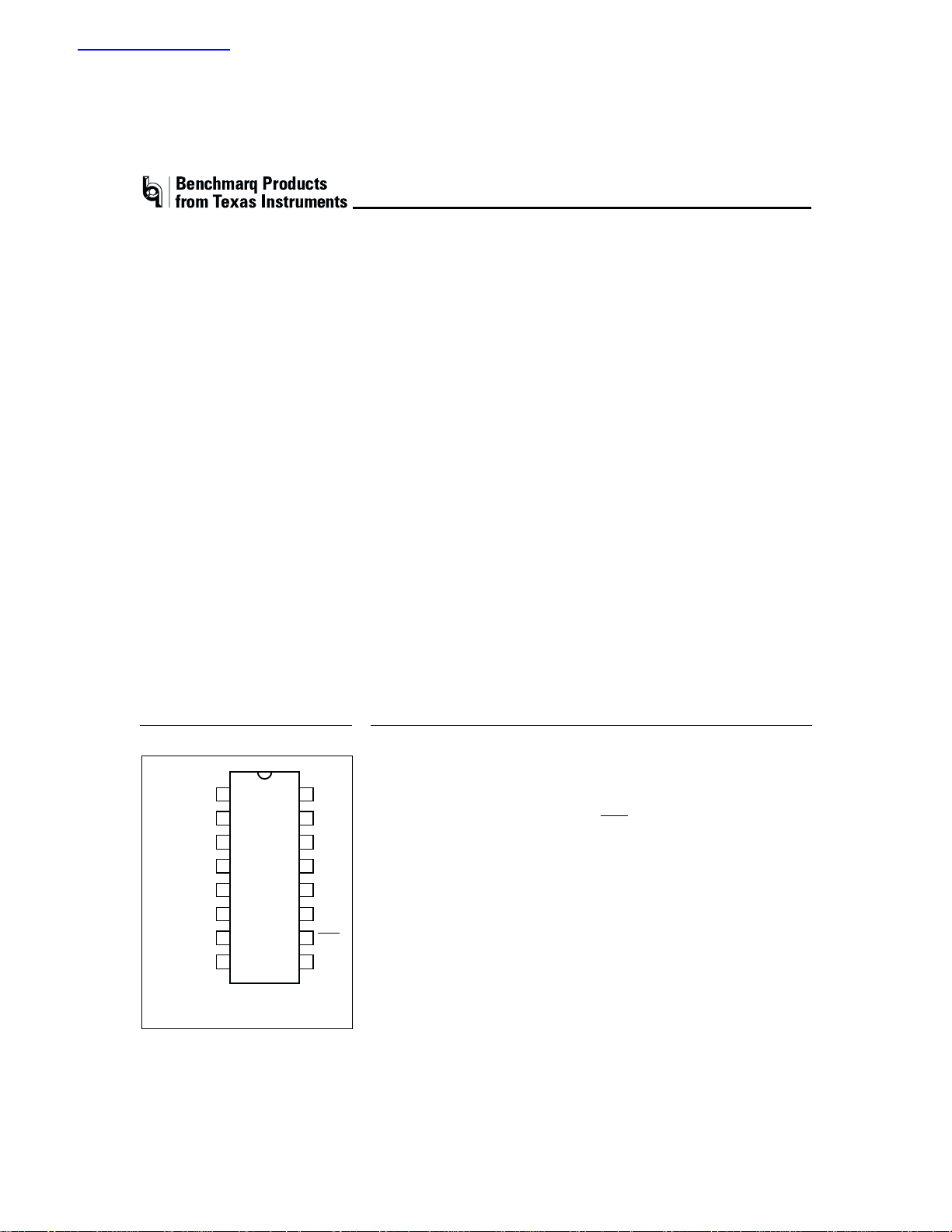
Pin Connections
LCOM
SEG1/PROG
SEG2/PROG
SEG3/PROG
SEG4/PROG
SEG5/PROG
PROG
SLUS019–MAY 1999
1
2
3
4
5
6
V
SS
16-Pin Narrow SOIC
1
2
3
4
5
6
7
8
Pin Names
LCOM LED common output
/PROG1LED segment 1/
16
V
15
REF
CP
14
13
HDQ
12
RBI
11
SB
10
DISP
9
SR
PN2052H1.eps
SEG
CC
1
/PROG2LED segment 2/
SEG
1
/PROG3LED segment 3/
SEG
1
/PROG4LED segment 4/
SEG
1
/PROG5LED segment 5/
SEG
1
CP Control port
program 1 input
program 2 input
program 3 input
program 4 input
program 5 input
1
V
SS
System ground
SR Sense resistor input
DISP
Display control input
SB Battery sense input
RBI Register backup input
HDQ Serial communications
input/output
6
Program 6 input
PROG
REF Voltage reference output
V
CC
Supply voltage

bq2052
Preliminary
Pin Descriptions
LCOM
SEG
SEG
PROG
PROG
PROG
PROG
PROG
PROG
V
SS
LED common output
This open-drain output switches V
source current for the LEDs. The switch is
off during initialization to allow reading of
the soft pull-up or pull-down program resis
tors. LCOM is also high impedance when the
display is off.
LED display segment outputs (dual func
–
1
tion with PROG
5
Each output may activate an LED to sink
the current sourced from LCOM.
Programmed full count selections
–
1
2
These three-level input pins define the pro
grammed full count.
Power gauge scale selection inputs (dual
3
function with SEG
This three-level input pin defines the scale
factor.
Programmed compensation factors
4
This three-level input pin defines the battery discharge compensation factors.
Programmed display mode
5
This three-level input pin defines the capac
ity indication display mode.
Programmed initial capacity state
6
This input defines the initial battery capac
ity indication state. When tied to V
bq2052 sets the available capacity to full on
reset. When tied to V
available capacity to zero on reset.
Ground
–PROG5)
1
–SEG4)
3
, the bq2052 sets the
SS
CC
CC
, the
SR
to
-
DISP
-
Sense resistor input
The voltage drop (V
is monitored and integrated over time
tor R
S
to interpret discharge activity. V
dicates discharge. The effective voltage drop,
V
, as seen by the bq2052 is VSR+VOS.
SRO
) across the sense resis
SR
SR>VSS
in
Display control input
high disables the LED display. DISP
DISP
tied to VCC(no display LEDs in the circuit)
allows PROG
V
instead of through a pull-up or
SS
pull-down resistor. DISP
to connect directly to VCCor
X
low activates the
-
-
display.
SB
-
Secondary battery input
This input monitors the battery cell voltage
potential through a high-impedance resis
tive divider network for the end-of-discharge
voltage (EDV) thresholds.
RBI
Register backup input
This pin is used to provide backup potential to
the bq2052 registers during periods when V
3V. A storage capacitor or a battery can be
≤
CC
connected to RBI.
HDQ
Serial communication input/output
This is the open-drain bidirectional communications port.
-
CP
Control port
This open drain output may be controlled by
serial port commands and its state is re
-
REF
flected in the CPIN bit in FLGS1.
Voltage reference output for regulator
-
REF provides a voltage reference output for
an optional micro-regulator.
V
CC
Supply voltage input
2
Preliminary
bq2052
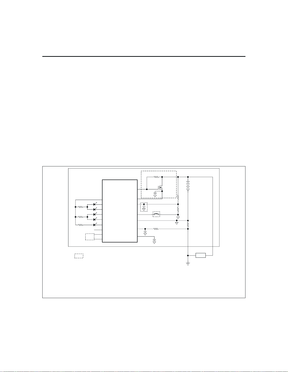
Functional Description
General Operation
The bq2052 determines battery capacity by monitoring
the amount of charge removed from a primary battery.
The bq2052 measures discharge currents and battery
voltage, monitors the battery for the low battery-voltage
thresholds, and compensates available capacity for tem
perature and discharge rate. The bq2052 measures ca
pacity by monitoring the voltage across a small-value se
ries sense resistor between the negative battery termi
nal and ground.
Figure 1 shows a typical battery pack application of the
bq2052 using the LED display capability as a
charge-state indicator. The bq2052 displays capacity
with two, four, or five LEDs using the programmed full
count (PFC) as the battery’s “full” reference. The bq2052
has a push-button input for momentarily enabling the
LED display.
bq2052
H or L
To µC
Gas Gauge IC
LCOM
SEG
1
SEG
2
SEG
3
SEG
4
SEG
5
PROG6
CP
HDQ
REF
V
CC
DISP
V
SR
RBI
SB
SS
Measurements
The bq2052 uses a voltage-to-frequency converter (VFC)
for discharge measurement and an analog-to-digital con
verter (ADC) for battery voltage measurement.
Discharge Counting
The VFC measures the discharge flow of the battery by
monitoring a small value sense resistor between the SR
pin and V
“discharge” activity when the potential at the SR input,
V
SRO
time using an internal counter. The fundamental rate of
the counter is 3.125µVh. The VFC measures signals up
to 0.5V in magnitude.
Digital Magnitude Filter
The bq2052 has a digital filter to eliminate discharge
counting below a set threshold. The minimum discharge
threshold, V
R
C
1
100K
0.1µF
as shown in Figure 1. The bq2052 detects
SS
, is positive. The bq2052 integrates the signal over
, for the bq2052 is 250µV.
SRD
1
Q1
ZVNL110A
RB
1
RB
2
R
S
-
Notes:
1.
2. VCC can connect directly to two lithium primary cells
(6.0V nominal and should not exceed 6.5V).
Otherwise, R1, C1, and Q1 are needed for regulation of > 2 cells.
3. Programming resistors and ESD-protection diodes are not shown.
4. R-C on SR is required.
5. A series diode is required on RBI if the bottom series cell is used as the backup source.
If the cell is used, the backup capacitor is not required, and the anode is connected to the
positive terminal of the cell.
Indicates optional.
Figure 1. Application Diagram—5-Segment LED Display
3
Load
FG205201.eps
bq2052
Preliminary
Table 1. bq2052 Current-Sensing Errors
Symbol Parameter Typical Maximum Units Notes
INL
INR
Integrated non-linearity
error
Integrated nonrepeatability error
2
±
1
±
4
±
2
±
Add 0.1% per °C above or below 25°C
%
and 1% per volt above or below 4.25V.
Measurement repeatability given
%
similar operating conditions.
Voltage Monitoring and Thresholds
In conjunction with monitoring the SR input for dis
charge currents, the bq2052 monitors the battery poten
tial through the SB pin. The voltage at the SB pin, V
is developed through a high impedance resistor network
connect across the battery. The bq2052 monitors the
voltage at the SB pin and reports the voltage in the VSB
register (address = 0bh).
The bq2052 compares the V
end-of-discharge voltage (EDV) thresholds. The EDV
reading to two
SB
threshold levels are used to determine when the battery
has reached an “empty” state. The EDV thresholds for
the bq2052 are programmable with the default values
fixed at:
EDV1 (first) = 0.76V
EDVF (final) = EDV1 - 0.10V = 0.66V
If V
is below either of the two EDV thresholds for 8
SB
consecutive samples over a 4 second period, the bq2052
sets the associated flag in the FLGS1 register (address =
01h). Once set, the EDV flags remain set, independent
of V
.
SB
Inputs
Main Counters
Discharge
Current
+
Discharge
Count
Register
(DCR)
SB
Temperature
The bq2052 has an internal temperature sensor to mea
sure temperature. The bq2052 determines the tempera
-
,
ture and stores it in the TEMP register (address = 02h).
The bq2052 uses temperature to adapt remaining capac
ity for the battery’s discharge efficiency.
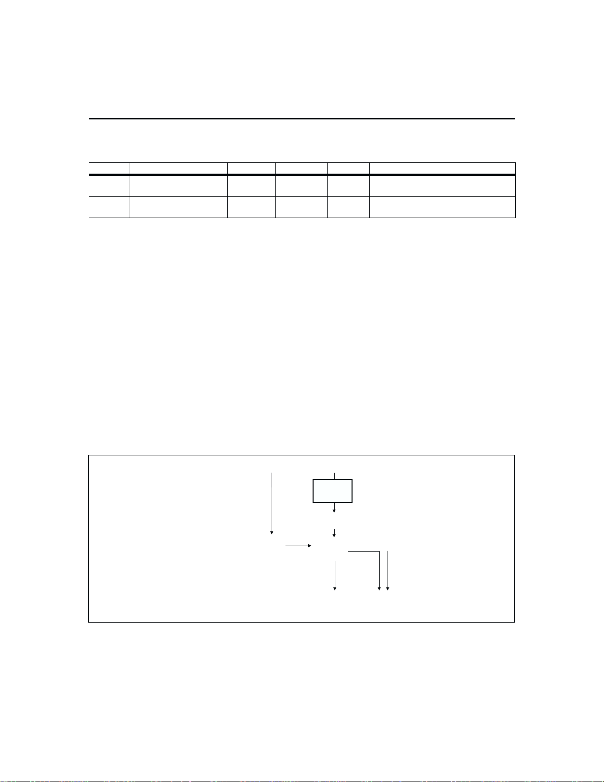
Gas Gauge Operation
General
The operational overview diagram in Figure 2 illustrates the operation of the bq2052. The bq2052 accumulates a measure of discharge currents and calculates
available capacity. The bq2052 compensates available
capacity for discharge rate and temperature and provides the information in the Compensated Available Capacity (CAC) registers (address = 0eh–0fh). The main
counter, Discharge Count Register (DCR) (address =
2eh), represents the cumulative amount of charge removed from the battery. Battery discharging increments
the DCR register.
Rate and
Temperature
Efficiency
Factor
Full Nominal
Available Charge
(FNAC)
–
+
Compensated
Available
Capacity
(CAC)
Complete
Data Set
-
-
-
Chip-Controlled
Outputs
Available Charge
LED Display
Figure 2. Operational Overview
4
Serial Port
FG2052.eps

Table 2. bq2052 Programmed Full Count mVh
Preliminary
bq2052
PROG
x
-- -
H H 48128 1203 602 301 mVh
H Z 46080 1152 576 288 mVh
H L 43264 1082 541 271 mVh
Z H 39936 998 499 250 mVh
Z Z 38400 960 480 240 mVh
Z L 36096 902 451 226 mVh
L H 31744 794 397 199 mVh
L Z 28928 723 362 181 mVh
L L 26112 653 327 164 mVh
Main Gas-Gauge Registers
Programmed Full Count
The PFC register stores the user-specified battery full
capacity. The 8-bit PFC registers stores the full capacity
in mVh scaled as shown in Table 2.
Full Nominal Available Capacity
The FNAC register stores the full capacity reference of
the battery. It can be programmed to initialize to PFC
or zero. The 8-bit FNAC register stores data scaled to
the same units as PFC. The bq2052 does not update
FNAC during the course of operation; therefore, if it is
programmed to 0 on initialization, it must be written to
full using the serial port.
Discharge Count Register
The DCR is the main gas gauging register and contains
the cumulative amount of discharge counted by the
bq2052. The 16-bit register stores data scaled to the
same units as PFC.
Compensated Available Capacity
The CAC registers contain the current available capac
ity of the battery. The data stored in CAC represents
the amount of remaining capacity of the battery compen
sated for rate and temperature use conditions. Tables 3,
4, and, 5 outline the options for typical efficiency com
pensation factors for lithium primary batteries. The
bq2052 applies the efficiency factors to FNAC to derive
CAC.
Programmed
Full Count
(PFC)
SCALE =
1/40
The bq2052 applies the compensation according to the
formula:
Where F
factor, FNAC = Full Nominal Available Capacity and
DCR = Discharge Count Register.
The bq2052 calculates an F
charge rate and temperature. The discharge rate portion of the F
therefore, the bq2052 latches the highest discharge rate
it has measured and uses the highest rate to calculate
F
CE
highest discharge rate measured by the bq2052 is stored
in MRATE (address = 12h).
The bq2052 does not latch the temperature portion of an
F
CE
crease during the course of a complete discharge cycle if
a temperature shift causes a change in the calculated
F
CE
Programming the bq2052
The bq2052 is programmed with the PROG
During power-up or initialization, the bq2052 reads the
state of these six three-level inputs and latches in the
programmable configuration settings.
-
PROG
3
SCALE =
1/80
CAC = [F
is the calculated efficiency compensation
CE
CE
throughout the complete discharge cycle. The
calculation. Therefore, CAC may increase or de
value.
CE
compensation is a “peak hold” function;
SCALE =
1/160
∗ FNAC] - DCR
based on the battery dis-
CE
1–6
Units12 H Z L
mVh/
count
-
pins.
7
5

bq2052
Preliminary
Programmable Configuration Settings
Design Capacity
The battery’s rated design capacity or Programmed Full
Count (PFC) is programmed with the PROG
pins as shown in Table 2, and represents the battery’s
full reference.
The correct PFC may be determined by multiplying the
rated battery capacity in mAh by the sense resistor
value:
Battery capacity (mAh)*sense resistor (Ω) = PFC
(mVh)
Selecting a PFC slightly less than the rated capacity
provides a conservative capacity reference. The bq2052
stores the selected PFC in the PFC register (address =
10h).
–PROG
1
Discharge Rate and Temperature Compensation
The discharge rate and temperature compensations are se
lected using the PROG
power-up or initialization determines which compensation
table the bq2052 uses for the discharge cycle. The following
tables illustrate the calculated efficiency compensation factors at selected discharge rates and temperatures.
pin. The level of PROG4on
4
Table 3. Discharge Efficiency Factor Table
PROG4 = Z
Discharge Rage
TEMP
-20 97 99 96 92 85 81
-10 98 98 97 94 89 85
21 99 99 98 96 92 89
55 99 99 98 96 93 90
70 99 99 98 96 93 90
0 C/80 C/25 C/10 C/5 C/3
0 989897949087
Table 4. Discharge Efficiency Factor Table
PROG4 = L
Discharge Rage
TEMP
-20 87 85 80 70 53 50
-10 93 91 88 80 68 51
21 99 97 95 89 81 68
55 100 99 97 92 85 74
70 101 100 98 93 86 76
0 C/80 C/25 C/10 C/5 C/3
0 969491857460
Table 5. Discharge Efficiency Factor Table
PROG4 = H
3
TEMP
-20 92 93 92 88 83 75
-10 98 98 97 93 89 81
0 100 100 99 96 91 84
21 104 104 102 99 95 88
55 106 106 105 100 97 90
70 107 107 105 101 98 91
0 C/80 C/25 C/10 C/5 C/3
Discharge Rage
Display Mode
The display mode is selected using the PROG5pin. The
three options include a two, four, or five segment display
mode as described in Tables 7, 8, and 9.
-
Initial Capacity Setting
The PFC value is copied to the FNAC register if PROG
is programmed high, otherwise FNAC defaults to 0.
FNAC may be written to the desired full capacity to initialize the pack manually.
Programming Example
Given:
Sense resistor = 0.05mΩ
Number of cells=5inseries
Capacity = 7000mAh,
Chemistry = LiSO
Discharge current range = 250mA to 2A
Voltage drop over sense resistor = 12.5mV to 100mV
Display mode = 5 segment bar graph display
Therefore:
7000mAh*0.05 = 350mVh
Select:
PFC = 26112 counts or 327mVh
PROG
= low
1
PROG
= low
2
PROG
= float
3
PROG
pensation factors
PROG
PROG
With these selections, the full battery capacity is
327mVh (6540mAh).
= float, high, or low depending on desired com
4
= float selects five segment display
5
= high sets FNAC to PFC
6
2
6
-
6

Preliminary
bq2052
Table 6. bq2052 Command and Status Registers
Loc.
Read/
(hex)
Symbol Register Name
CMDWD Command word 00h W CMD7 CMD6 CMD5 CMD4 CMD3 CMD2 CMD1 CMD0
FLGS1 Primary status flags 01h R INIT RSVD RSVD CPIN RSVD RSVD EDV1 EDVF
TEMP
NAC
BATID Battery identification 04h R/W BATID7 BATID6 BATID5 BATID4 BATID3 BATID2BATID1 BATID0
VSRL Current scale (Low) 05h R VSRL7 VSRL6 VSRL5 VSRL4 VSRL3 VSRL2 VSRL1 VSRL0
VSRH Current scale (High) 06h R VSRH7 VSRH6 VSRH5 VSRH4 VSRH3 VSRH2 VSRH1 VSRH0
PPD
PPU Program pin pull-up 08h R RSVD RSVD PPU6 PPU5 PPU4 PPU3 PPU2 PPU1
VSB
VTS
RCAC
CACL
CACH
PFC Program pin full count 10h R PFC7 PFC6 PFC5 PFC4 PFC3 PFC2 PFC1 PFC0
FNAC
MAX
RATE
RATE Discharge rate 13h R RATE7 RATE6 RATE5 RATE4 RATE3 RATE2 RATE1 RATE0
DCRL
DCRH
Notes: RSVD = reserved.
Temperature (°C)
Nominal available
capacity
Program pin pulldown
Battery voltage
register
End-of-discharge
threshold select
register
Relative compensated
capacity
Compensated available capacity low byte
Compensated available
capacity high byte
Full nominal
available capacity
Maximum discharge
rate
Discharge count
register (low byte)
Discharge count
register (high byte)
All other registers not documented are reserved.
Write
02h R TEMP7 TEMP6 TEMP5 TEMP4 TEMP3 TEMP2 TEMP1 TEMP0
03h R/W NAC7 NAC6 NAC5 NAC4 NAC3 NAC2 NAC1 NAC0
07h R RSVD RSVD PPD6 PPD5 PPD4 PPD3 PPD2 PPD1
0bh R VSB7 VSB6 VSB5 VSB4 VSB3 VSB2 VSB1 VSB0
0ch R/W VTS7 VTS6 VTS5 VTS4 VTS3 VTS2 VTS1 VTS0
0dh R RSVD RCAC6 RCAC5 RCAC4 RCAC3 RCAC2 RCAC1 RCAC0
0eh R CACL7 CACL6 CACL5 CACL4 CACL3 CACL2 CACL1 CACL0
0fh R CACH7 CACH6 CACH5 CACH4 CACH3 CACH2 CACH1 CACH0
11h R/W FNAC7 FNAC6 FNAC5 FNAC4 FNAC3 FNAC2 FNAC1 FNAC0
12h R MAX7 MAX6 MAX5 MAX4 MAX3 MAX2 MAX1 MAX0
2eh R/W DCRL7 DCRL6 DCRL5 DCRL4 DCRL3 DCRL2 DCRL1 DCRL0
2fh R/W DCRH7 DCRH6 DCRH5 DCRH4 DCRH3 DCRH2 DCRH1 DCRH0
Control Field
76543210
7

bq2052
Preliminary
Break
Send Host to bq-HDQ
CDMR
LSB
Bit0
Start-bit
Address
Address-Bit/
Data-Bit
Send Host to bq-HDQ or
Stop-Bit
Figure 4. bq2052 Communication Example
Written by Host to bq2052
Received by Host to bq2052
CMDR = 03h
Receive from bq-HDQ
Data
R/W
MSB
Bit7
TD201807.eps
NAC = 65h
t
RSPS
t
RR
LSB MSB LSB MSB
Break 0 0 0000 1010011
110
HDQ
t
RSPS
Figure 5. Typical Communication with the bq2052
8
TD2052TC.eps

Preliminary
bq2052
Communicating With the bq2052
The bq2052 includes a simple single-pin (HDQ plus re
turn) serial data interface. A host processor uses the in
terface to access various bq2052 registers. Battery char
acteristics may be easily monitored by adding a single
contact to the battery pack. The open-drain HDQ pin on
the bq2052 should be pulled up by the host system, or
may be left floating if the serial interface is not used.
The interface uses a command-based protocol, where the
host processor sends a command byte to the bq2052.
The command directs the bq2052 to either store the next
eight bits of data received to a register specified by the
command byte or output the eight bits of data specified
by the command byte.
The communication protocol is asynchronous re
turn-to-one. Command and data bytes consist of a
stream of eight bits that have a maximum transmission
rate of 5K bits/sec. The least-significant bit of a com
mand or data byte is transmitted first. The protocol is
simple enough that it can be implemented by most host
processors using either polled or interrupt processing.
Data input from the bq2052 may be sampled using the
pulse-width capture timers available on some
microcontrollers.
If a communication error occurs, e.g., t
bq2052 should be sent a BREAK to reinitiate the serial
interface. A BREAK is detected when the HDQ pin is
driven to a logic-low state for a time, t
HDQ pin should then be returned to its normal
ready-high logic state for a time, t
ready to receive a command from the host processor.
The return-to-one data bit frame consists of three dis
tinct sections. The first section is used to start the
transmission by either the host or the bq2052 taking the
HDQ pin to a logic-low state for a period, t
next section is the actual data transmission, where the
data should be valid by a period, t
tive edge used to start communication. The data should
be held for a period, t
to sample the data bit.
The final section is used to stop the transmission by re
turning the HDQ pin to a logic-high state by at least a pe
riod, t
nication. The final logic-high state should be until a pe
riod t
mission was stopped properly. The timings for data and
break communication are given in the serial communica
tion timing specification and illustration sections.
Communication with the bq2052 is always performed
with the least-significant bit being transmitted first.
Figure 5 shows an example of a communication se
quence to read the bq2052 NAC register.
, after the negative edge used to start commu
SSU;B
, to allow time to ensure that the bit trans
CYCH;B
, to allow the host or bq2052
DH;DV
. The bq2052 is now
BR
DSU;B
> 250µs, the
CYCB
or greater. The
B
STRH;B
, after the nega
. The
bq2052 Command Code and
Registers
-
The bq2052 status registers are listed in Table 6 and de
scribed below.
Command Code
The bq2052 latches the command code when eight valid
command bits have been received by the bq2052. The
command code contains two fields:
W/R bit
■
Command address
■
The W/R
the received command is for a read or a write function.
-
The W/R
-
Where W/R is:
The lower seven-bit field of the command code contains
the address portion of the register to be accessed. At
tempts to write to invalid addresses are ignored.
-
-
-
Command Word (CMDWD)
-
The CMDWD register (address = 00h) is used by the ex
ternal host to control the CP pin and to reset the
bq2052.
-
CMDWD Action
-
bit of the command code is used to select whether
values are:
Command Code Bits
76543 2 1 0
W/R
- -- - - - -
0 The bq2052 outputs the requested register con-
tents specified by the address portion of command code.
1 The following eight bits should be written to the
register specified by the address portion of command code.
Command Code Bits
7654 3 2 1 0
- AD6 AD5 AD4 AD3 AD2 AD1
0x55 CP high impedence, CPIN bit in FLGS1 set
0x66 CP driven low, CPIN bit in FLGS1 cleared
0x78 bq2052 reset
-
-
AD0
(LSB)
-
9

bq2052
Preliminary
Primary Status Flags Register (FLGS1)
The FLGS1 register (address = 01h) contains the pri
mary bq2052 flags.
The initialized flag (INIT) is asserted to a 1 or 0 when
ever the bq2052 is initialized either by the application of
Vcc or by a serial port command. INIT = 1 signifies that
the device has been reset with FNAC set to PFC. INIT = 0
signifies that the battery has been reset with FNAC = 0.
The INIT location is:
FLGS1 Bits
765 4 3 2 1 0
INIT - - - - - - -
where INIT is:
0 The bq2052 initialized with FNAC = 0.
1 The bq2052 initialized with FNAC = PFC.
The CPIN but reflects the state of the CP output. If set,
the CP output is high impedance. If cleared, the CP output is asserted low. The CP output is an open drain output and requires an external pull-up register.
The CPIN location is
FLGS1 Bits
76543210
- - - CPIN ----
Where CPIN is:
0 CP is low
1 CP is high impedance
The bq2052 sets the first end-of-discharge warning
flag (EDV1) when the battery voltage VSB is less than
the EDV1 threshold VTS. The flag warns the user that
the battery is almost empty. The bq2052 modulates the
first segment pin, SEG1, at a 4Hz rate if the 4 or 5 seg
ment display mode is enabled and EDV1 is asserted.
The EDV1 threshold has a default value of 0.76V but
can be adjusted by writing the VTS register .
The EDV1 location is
FLGS1 Bits
765 4 3 2 1 0
- - - - - - EDV1 -
Where EDV1 is:
0V
SB
V
≥
TS
1VSB<V
The bq2052 sets the final end-of-discharge warning
flag (EDVF) when VSB is less than the EDVF threshold.
The EDVF threshold is set 100mV below the EDV1
threshold. The EDVF flag is used to warn the system or
user that battery power is at a failure condition. The
bq2052 turns all segment drivers off upon EDVF detec
tion.
The EDVF location is:
765 4 3 2 1 0
--- - - - -EDVF
Where EDVF is:
0V
1V
TS
- 100mV)
(V
≥
SB
TS
< (VTS-100mV)
SB
FLGS1 Bits
Temperature Register (TEMP)
The 8-bit TEMP register (address=02h) contains the
battery temperature in degrees C. The bq2052 contains
an internal temperature sensor. The temperature is
used to set discharge efficiency factors. The temperature
register contents are store in 2’s complement form and
represent the temperature ± 5°C.
Nominal Available Capacity Register (NAC)
The NAC register contains the uncompensated remaining
capacity of the battery. The bq2052 determines NAC as
NAC = FNAC - DCR
Battery Identification Register (BATID)
The 8-bit BATID register (address=04h) is a general
purpose memory register that can be used to uniquely
identify a battery pack. The bq2052 maintains the
BATID contents as long as VRBI is greater than 2V. The
contents of this register have no effect on the operation
of the bq2052.
Current Scale Registers (VSRL/VSRH)
The VSRH high-byte register and the VSRL low-byte
register are used to calculate the average signal across
the SR and VSS pins. This register pair is updated ev
ery 5.625 seconds. VSRH and VSRL form a 16-bit value
representing the average current over this time. The
battery pack current can be calculated by:
(VSRH 256 + VSRL)
|I(mA)| =
∗
S
(R )
-
-
10

Preliminary
bq2052
where
= sense resistor value in Ω.
R
S
VSRH = high-byte value of current scale
VSRL = low-byte value of current scale
Program Pin Pull-Down Register (PPD)
The PPD register (address = 07h) contains the pull-down
programming pin information for the bq2052. The pro
gram pins, PROG
location, PPD
detects a pull-down resistor on its corresponding seg
ment driver. For example, if PROG
pull-down resistors,the contents of PPD are xx001001.
, have a corresponding PPD register
1–6
. A given location is set if the bq2052
1–6
and PROG4have
1
Program Pin Pull-Up Register (PPU)
The PPU register (address = 08h) contains the pull-up
programming pin information for the bq2052. The seg
ment drivers, PROG
ister location, PPU
pull-up resistor has been detected on its corresponding
segment driver. For example, if PROG
have pull-up resistors, the contents of PPU are
xx010100.
, have a corresponding PPU reg
1–6
. A given location is set if a
1–6
and PROG
3
Battery Voltage (VSB)
The battery voltage register (address = 0bh) stored the
voltage detected on the SB pin. The bq2052 updates the
VSB register approximately once per second with the
present value of the battery voltage.
VSB
V
= 1.2V
SB
∗
256
temperature. The CAC value is also used in calculating
the LED display pattern relative to PFC.
Program Full Count (PFC)
The PFC register (address = 10h) contains the user se
lected programmed full count (PFC) setting.
Full Nominal Available Capacity (FNAC)
The FNAC (address = 11h) contains the full capacity
reference of the battery.
Maximum Discharge Rate (MAXRATE)
-
The MAXRATE register (address = 12h) stores the high
est discharge rate detected by the bq2052. The bq2052
uses the MAXRATE value to calculate the efficiency
compensation factors.
Discharge Rate (RATE)
-
The RATE register (address = 13h) provides the current
discharge rate of the battery.
5
Discharge Count Registers (DCRH/DCRL)
The DCRH high-byte register and the DCRL low-byte
register are the main gas gauging registers for the
bq2052. The DCR registers are incremented during discharge.
Writing to the DCR registers affects the available charge
counts and, therefore, affects the bq2052 gas gauge operation.
Display
-
-
Voltage Threshold Register (VTS)
The end-of-discharge threshold voltages (EDV1 and
EDVF) can be set using the VTS register. The VTS reg
ister sets the EDV1 trip point. EDVF is set 100mV below
EDV1. The default value in the VTS register is A2h,
representing EDV1 = 0.76V and EDVF = 0.66V.
VTS
EDV1 = 1.2V
*
.
256
Relative CAC Register (RCAC)
The RCAC register (address = 0dh) provides the relative
battery state-of-charge by dividing CAC by FNAC.
RCAC varies from 0 to 7dh representing relative
state-of-charge from 0 to 125%.
Compensated Available Capacity (CAC)
The CAC registers (address = 0eh–0fh) contain the
available capacity compensated for discharge rate and
The bq2052 can directly display remaining capacity in
formation using low-power LEDs. The bq2052 uses the
CAC value in relation to FNAC as the basis for the dis
-
play activity. The bq2052 displays the battery’s remain
ing capacity in either of three modes selected with pro
gram pin PROG
DISP
input. When DISP is connected to VCC, the SEG
outputs are OFF. When pulled low, the segment outputs
turn ON for a period of 4 ± 0.5s, depending on the se
lected mode.
The segment outputs are modulated as two banks, with
segments 1, 3, and 5 alternating with segments 2 and 4.
The segment outputs are modulated at approximately
100Hz with each segment bank active for 30% of the pe
riod. In incremental and bar graph modes, SEG1 blinks
at a 4Hz rate whenever VSB is below VEDV1 (EDV1
flag bit set in FLGS1), indicating a low-battery condi
tion. When VSB is below VEDVF (EDVF flag bit set in
FLGS1) the display outputs are disabled in all modes.
. The display is activated using the
5
11
-
-
-
-
-
-
-

bq2052
Preliminary
In incremental mode (PROG5= L), the battery charge
state is displayed on pins SEG1–SEG4. The charge state
condition indicated by each segment is shown in Table 7.
Only the segment pin representing the present remain
ing capacity is ON (low); all other segments are OFF
(high impedance). When DISP
is active for 10s.
is pulled low, the display
Table 7. Incremental Display Mode
PROG
SEG Pin ON Remaining Capacity
SEG4 90 -100%
SEG3 50 - < 90%
SEG2 20 - < 50%
SEG1 < 20%
SEG1—BLINK V
In binary mode (PROG5 = H), the battery charge state is
displayed using only pins SEG1 and SEG2, with the re
maining capacity indication defined as in Table 8. When
DISP
is pulled low, the display is active for 4s.
5
= L
SB
< V
EDV1
Table 8. Binary Display Mode
PROG
SEG 1 SEG 2 Remaining Capacity
ON ON 70 -100%
ON OFF 40 - < 70%
OFF ON 10 - < 40%
OFF OFF < 10% or V
5
= H
SB
< V
EDVF
Microregulator
A micro-power source for the bq2052 can be inexpen
sively built using a FET and an external resistor as
shown in Figure 1.
RBI Input
The RBI input pin should be used with a storage capaci
tor or external supply to provide backup potential to the
internal bq2052 registers when V
V
is output on RBI when VCCis above 3.0V. If using
CC
an external supply (such as the bottom series cell) as the
backup source, an external diode is required for isola
tion.
drops below 3.0V.
CC
Initialization
The bq2052 can be initialized by removing VCCand
grounding the RBI pin for 5s or by a command over the
serial port. The serial port reset command requires
writing 78h to register CMDWD (address = 00h).
On initialization with PROG6 = H, the bq2052 sets the
registers as
FNAC = PFC
CACH = PFC
CACL = 0x00
RCAC = 0x64
FLGS1 = 0x90
-
-
-
In bar graph mode (PROG5= Z), the battery charge
state is displayed using pins SEG1 through SEG 5 ac
cording to Table 9. When DISP
is active for 4s.
is pulled low, the display
-
Table 9. Bar Graph Display Mode
12
= Z
5
PROG
SEG1 SEG2 SEG3 SEG4 SEG5 Remaining Capacity
ON ON ON ON ON 80 - 100%
ON ON ON ON OFF 60 - < 80%
ON ON ON OFF OFF 40 - < 60%
ON ON OFF OFF OFF 20 - < 40%
ON OFF OFF OFF OFF < 20%
BLINK OFF OFF OFF OFF VSB < VEDV1

Preliminary
bq2052
On initialization with PROG6=L, the bq2052 sets the
registers as
FNAC = 0x00
CACH = 0x00
CACL = 0x00
RCAC = 0x00
FLGS1 = 0x10
Layout Considerations
The bq2052 measures the voltage differential between
the SR and V
pin) is greatly affected by PC board layout. For optimal
results, the PC board layout should follow the strict rule
of a single-point ground return. Sharing high-current
ground with small signal ground causes undesirable
noise on the small signal nodes.
pins. VOS(the offset voltage at the SR
SS
Absolute Maximum Ratings
Symbol Parameter Minimum Maximum Unit Notes
V
CC
All other pins Relative to V
REF Relative to V
V
SR
T
OPR
Note: Permanent device damage may occur if Absolute Maximum Ratings are exceeded. Functional
Relative to V
Relative to V
Operating temperature -20 +70 °C Commercial
operation should be limited to the Recommended DC Operating Conditions detailed in this data sheet.
Exposure to conditions beyond the operational limits for extended periods of time may affect device reliability.
SS
SS
SS
SS
-0.3 +7.0 V
-0.3 +7.0 V
-0.3 +8.5 V Current limited by R1 (see Figure 1)
-0.3 Vcc+0.7 V
Recommended 100KΩseries resistor
should be used to protect SR in case
of a shorted battery.
DC Voltage Thresholds (T
Symbol Parameter Minimum Typical Maximum Unit Notes
V
EDV1
V
EDVF
V
SRO
V
SRD
Note: VOSis affected by PC board layout. Proper layout guidelines should be followed for optimal performance.
First empty warning 0.73 0.76 0.79 V SB, default
Final empty warning - V
SR sense range -300 - +500 mV SR, VSR+ V
Valid discharge - - -250
See “Layout Considerations.”
= T
A
; V = 3.0 to 6.5V)
OPR
- 0.10 - V SB, default
EDV1
VVSR+ VOS(see note)
µ
OS
13

bq2052
Preliminary
DC Electrical Characteristics (T
=T
OPR
)
A
Symbol Parameter Minimum Typical Maximum Unit Notes
excursion from < 2.0V to
V
V
CC
V
OS
V
REF
R
REF
I
CC
V
SB
R
SBmax
I
DISP
I
LCOM
I
RBI
R
HDQ
R
SR
V
IHPFC
V
ILPFC
V
IZPFC
V
OLSL
V
OLSH
V
OHML
V
OHMH
I
OLS
I
OL
V
OL
V
IHDQ
V
ILDQ
R
PROG
R
FLOAT
Supply voltage 3.0 4.25 6.5 V
Offset referred to V
SR
-
±50 ±150 µV
Reference at 25°C 5.7 6.0 6.3 V I
Reference at -40°C to +85°C 4.5 - 7.5 V I
Reference input impedance 2.0 5.0 - MΩV
- 90 135
Normal operation
- 120 180
- 170 250
Battery input 0 - V
CC
µA
µA
µA
SB input impedance 10 - - MΩ0 < VSB<V
DISP input leakage - - 5
LCOM input leakage -0.2 - 0.2
µA
µA
RBI data retention current - - 100 nA V
Internal pulldown 500 - - K
SR input impedance 10 - - MΩVSR<V
PROG logic input high VCC- 0.2 - - V PROG
PROG logic input low - - VSS+ 0.2 V PROG
PROG logic input Z float - float V PROG
SEG output low, low V
SEG output low, high V
CC
CC
LCOM output high, low V
LCOM output high, high V
CC
CCVCC
- 0.1 - V
- 0.4 - V
VCC- 0.3
- 0.6
--V
--V
SEG sink current 11.0 - - mA At V
Open-drain sink current 5.0 - - mA At VOL=VSS+ 0.3V, HDQ
Open-drain output low - - 0.3 V I
HDQ input high 2.5 - - V HDQ
HDQ input low - - 0.8 V HDQ
Soft pull-up or pull-down resis
tor value (for programming)
-
- - 200
KΩ
Float state external impedance - 5 - MΩPROG
CC
3.0V initializes the unit.
≥
=V
DISP
= 5µA
REF
= 5µA
REF
= 3V
REF
= 3.0V, HDQ = 0
V
CC
V
= 4.25V, HDQ = 0
CC
= 6.5V, HDQ = 0
V
CC
V
V
DISP=VSS
=V
DISP
RBI>VCC
Ω
CC
1-6
1-6
1-6
= 3V, I
V
CC
SEG
, CP
1–5
= 6.5V, I
V
CC
SEG
, CP
1–5
VCC= 3V, I
-5.25mA
> 3.5V, I
V
CC
-33.0mA
OLSH
5mA, HDQ
≤
OL
PROG
–PROG
1
1–6
CC
CC
CC
< 3V
OLS
OLS
OHLCOM
OHLCOM
= 0.4V, VCC= 6.5V
Note: All voltages relative to VSS.
≤
6
1.75mA
11.0mA
≤
=
=
14

Preliminary
bq2052
Serial Communication Timing Specification (T
Symbol Parameter Minimum Typical Maximum Unit Notes
t
CYCH
t
CYCB
t
STRH
t
STRB
t
DSU
t
DSUB
t
DH
t
DV
t
SSU
t
SSUB
t
RSPS
t
B
t
BR
Note: The open-drain HDQ pin should be pulled to at least VCCby the host system for proper HDQ operation.
Cycle time, host to bq2052 (write) 190 - -
Cycle time, bq2052 to host (read) 190 205 250
Start hold, host to bq2052 (write) 5 - - ns
Start hold, bq2052 to host (read) 32 - -
Data setup - - 50
Data setup - - 50
Data hold 90 - -
Data valid - - 80
Stop setup - - 145
Stop setup - - 145
Response time, bq2052 to host 190 - 320
Break 190 - -
Break recovery 40 - -
HDQ may be left floating if the serial interface is not used.
=T
A
OPR
)
s See note
µ
s
µ
s
µ
s
µ
µs
s
µ
s
µ
s
µ
s
µ
µs
s
µ
s
µ
15

bq2052
Preliminary
Break Timing
Host to bq2052
bq2052 to Host
t
STRH
t
DSU
t
DH
t
SSU
t
B
Write "1"
Write "0"
t
CYCH
t
BR
TD201803.eps
t
STRB
t
DSUB
t
DV
t
SSUB
Read "1"
Read "0"
t
CYCB
16

16-Pin SOIC Narrow (SN)
Preliminary
bq2052
16-Pin SN(SOIC Narrow
Dimension Minimum Maximum
D
e
B
E
H
A 0.060 0.070
A1 0.004 0.010
B 0.013 0.020
C 0.007 0.010
D 0.385 0.400
E 0.150 0.160
e 0.045 0.055
H 0.225 0.245
L 0.015 0.035
All dimensions are in inches.
)
A
C
A1
.004
L
Ordering Information
bq2052
Temperature Range:
blank = Commercial (-20 to +70°C)
Package Option:
SN = 16-pin narrow SOIC
Device:
bq2052 Gas Gauge IC
17

IMPORTANT NOTICE
Texas Instruments and its subsidiaries (TI) reserve the right to make changes to their products or to discontinue any
product or service without notice, and advise customers to obtain the latest version of relevant information to verify,
before placing orders, that information being relied on is current and complete. All products are sold subject to the
terms and conditions of sale supplied at the time of order acknowledgement, including those pertaining to warranty,
patent infringement, and limitation of liability.
TI warrants performance of its semiconductor products to the specifications applicable at the time of sale in accor
dance with TI’s standard warranty. Testing and other quality control techniques are utilized to the extent TI deems
necessary to support this warranty. Specific testing of all parameters of each device is not necessarily performed, ex
cept those mandated by government requirements.
CERTAIN APPLICATIONS USING SEMICONDUCTOR PRODUCTS MAY INVOLVE POTENTIAL RISKS OF DEATH,
PERSONAL INJURY, OR SEVERE PROPERTY OR ENVIRONMENTAL DAMAGE (“CRITICAL APPLICATIONS”). TI
SEMICONDUCTOR PRODUCTS ARE NOT DESIGNED, AUTHORIZED, OR WARRANTED TO BE SUITABLE FOR
USE IN LIFE-SUPPORT DEVICES OR SYSTEMS OR OTHER CRITICAL APPLICATIONS. INCLUSION OF TI
PRODUCTS IN SUCH APPLICATIONS IS UNDERSTOOD TO BE FULLY AT THE CUSTOMER’S RISK.
In order to minimize risks associated with the customer’s applications, adequate design and operating safeguards
must be provided by the customer to minimize inherent or procedural hazards.
TI assumes no liability for applications assistance or customer product design. TI does not warrant or represent that
any license, either express or implied, is granted under any patent right, copyright, mask work right, or other intellec
tual property right of TI covering or relating to any combination, machine, or process in which such semiconductor
products or services might be or are used. TI’s publication of information regarding any third party’s products or ser
vices does not constitute TI’s approval, warranty or endorsement thereof.
-
-
-
-
Copyright © 1999, Texas Instruments Incorporated
18
 Loading...