

Page 1

查询BQ2050H供应商
bq2050H
Low-Cost Lithium Ion Power Gauge™ IC
Features
Accurate measurement of avail
➤
able capacity in Lithium Ion bat
teries
Provides a low-cost battery man
➤
agement solution for pack
integration
Complete circuit can fit in as
-
little as
Low operating current (120µA
-
1
square inch of PCB
2
typical)
Less than 100nA of data
-
retention current
High-speed (5kb) single-wire
➤
communication interface (HDQ
bus) for critical battery
parameters
➤ Monitors and controls charge FET
in Li-Ion pack protection circuit
➤ Direct drive of remaining capacity
LEDs
➤ Measurements automatically
compensated for rate and
temperature
➤ 16-pin narrow SOIC
-
General Description
The bq2050H Lithium Ion Power
Gauge™ IC is intended for battery-
pack or in-system installation to
maintain an accurate record of
available battery capacity. The IC
monitors a voltage drop across a
sense resistor connected in series
between the negative battery termi
nal and ground to determine
charge and discharge activity of
the battery. Compensations for bat
tery temperature, self discharge,
and rate of discharge are applied to
the charge counter to provide avail
able capacity information across a
wide range of operating conditions.
Battery capacity is automatically re
calibrated, or “learned,” in the
course of a discharge cycle from full
to empty.
Nominal available capacity may be
directly indicated using a fivesegment LED display. These seg-
ments are used to graphically indi
cate available capacity. The
bq2050H also supports a simple
single-line bidirectional serial link
to an external processor (common
ground). The 5kb HDQ bus interface
reduces communications overhead
in the external microcontroller.
Internal registers include available
capacity, temperature, scaled avail
able energy, battery ID, battery
status, and Li-Ion charge FET
status. The external processor may
also overwrite some of the bq2050H
power gauge data registers.
The bq2050H can operate from the
batteries in the pack. The REF out
-
put and an external transistor allow
a simple, inexpensive voltage regulator to supply power to the circuit
from the cells.
-
-
-
Pin Connections
1
LCOM
SEG1/PROG
SEG2/PROG
SEG3/PROG
SEG4/PROG
SEG5/PROG
SLUS150–MAY 1999 D
1
2
3
4
5
CFC
V
SS
16-Pin Narrow SOIC
16
2
15
3
14
4
13
5
12
6
11
7
10
8
Pin Names
LCOM LED common output
/PROG1LED segment 1/
SEG
1
V
CC
REF
PSTAT
HDQ
RBI
SB
DISP
9
SR
PN2050H1.eps
/PROG2LED segment 2/
SEG
2
/PROG3LED segment 3/
SEG
3
/PROG4LED segment 4/
SEG
4
/PROG5LED segment 5/
SEG
5
CFC Charge FET control
program 1 input
program 2 input
program 3 input
program 4 input
program 5 input
output
1
V
SS
System ground
SR Sense resistor input
DISP
Display control input
SB Battery sense input
RBI Register backup input
HDQ Serial communications
input/output
PSTAT Protector status input
REF Voltage reference output
V
CC
Supply voltage
Page 2

bq2050H
Pin Descriptions
LCOM
SEG
SEG
PROG
PROG
PROG
PROG
PROG
CFC
V
SS
SR
LED common output
This open-drain output switches V
source current for the LEDs. The switch is
off during initialization to allow reading of
the soft pull-up or pull-down program resis
tors. LCOM is also high impedance when the
display is off.
LED display segment outputs (dual func
–
1
tion with PROG
5
Each output may activate an LED to sink
the current sourced from LCOM.
Programmed full count selection inputs
–
1
(dual function with SEG
2
These three-level input pins define the pro
grammed full count (PFC) thresholds de
scribed in Table 2.
Power gauge scale selection inputs (dual
–
3
function with SEG
4
These three-level input pins define the scale
factor described in Table 2.
Self-discharge rate selection (dual func-
5
tion with SEG
This three-level input pin defines the
self-discharge and battery compensation factors as shown in Table 1.
Charge FET control output
This pin can be used as an additional control
to the charge FET of the Li-Ion pack protec
tion circuitry.
Ground
Sense resistor input
The voltage drop (V
sistor R
time to interpret charge and discharge activ
is monitored and integrated over
S
ity. The SR input is tied between the nega
tive terminal of the battery and the sense re
sistor. V
V
voltage drop, V
is V
SR<VSS
SR>VSS
SR+VOS
CC
–PROG5)
1
–SEG2)
1
–SEG4)
3
)
5
) across the sense re
SR
indicates discharge, and
indicates charge. The effective
, as seen by the bq2050H
SRO
.
to
-
-
-
-
-
-
-
-
-
DISP
SB
RBI
HDQ
PSTAT
REF
V
CC
Display control input
high disables the LED display. DISP
DISP
tied to VCCallows PROGXto connect di
rectly to V
pull-up or pull-down resistor. DISP
or VSSinstead of through a
CC
floating
allows the LED display to be active during
charge. DISP
low activates the display. See
Table 1.
Secondary battery input
This input monitors the battery cell voltage
potential through a high-impedance resis
tive divider network for end-of-discharge
voltage (EDV) thresholds and battery-removed
detection.
Register backup input
This pin is used to provide backup potential to
the bq2050H registers during periods when
V
3V. A storage capacitor or a battery
≤
CC
can be connected to RBI.
Serial communication input/output
This is the open-drain bidirectional communications port.
Protector status input
This input provides overvoltage status from
the Li-Ion protector circuit. It should connect to V
when not used.
SS
Voltage reference output for regulator
REF provides a voltage reference output for
an optional micro-regulator.
Supply voltage input
-
-
2
Page 3
bq2050H
Functional Description
General Operation
The bq2050H determines battery capacity by moni
toring the amount of current input to or removed
from a rechargeable battery. The bq2050H meas
ures discharge and charge currents, measures bat
tery voltage, estimates self-discharge, monitors the
battery for low battery-voltage thresholds, and com
pensates for temperature and discharge rate. Cur
rent measurement is measured by monitoring the
voltage across a small-value series sense resistor be
tween the negative battery terminal and ground.
Scaled available energy is estimated using the re
maining average battery voltage during the dis
charge cycle and the remaining nominal available
bq2050H
Power Gauge IC
LCOM
SEG1/PROG
SEG2/PROG
SEG3/PROG
SEG4/PROG
SEG5/PROG
CFC
PSTAT
REF
V
CC
SB
1
2
DISP
3
4
SR
5
V
SS
RBI
HDQ
capacity. The scaled available energy measurement
is corrected for environmental and operating condi
tions.
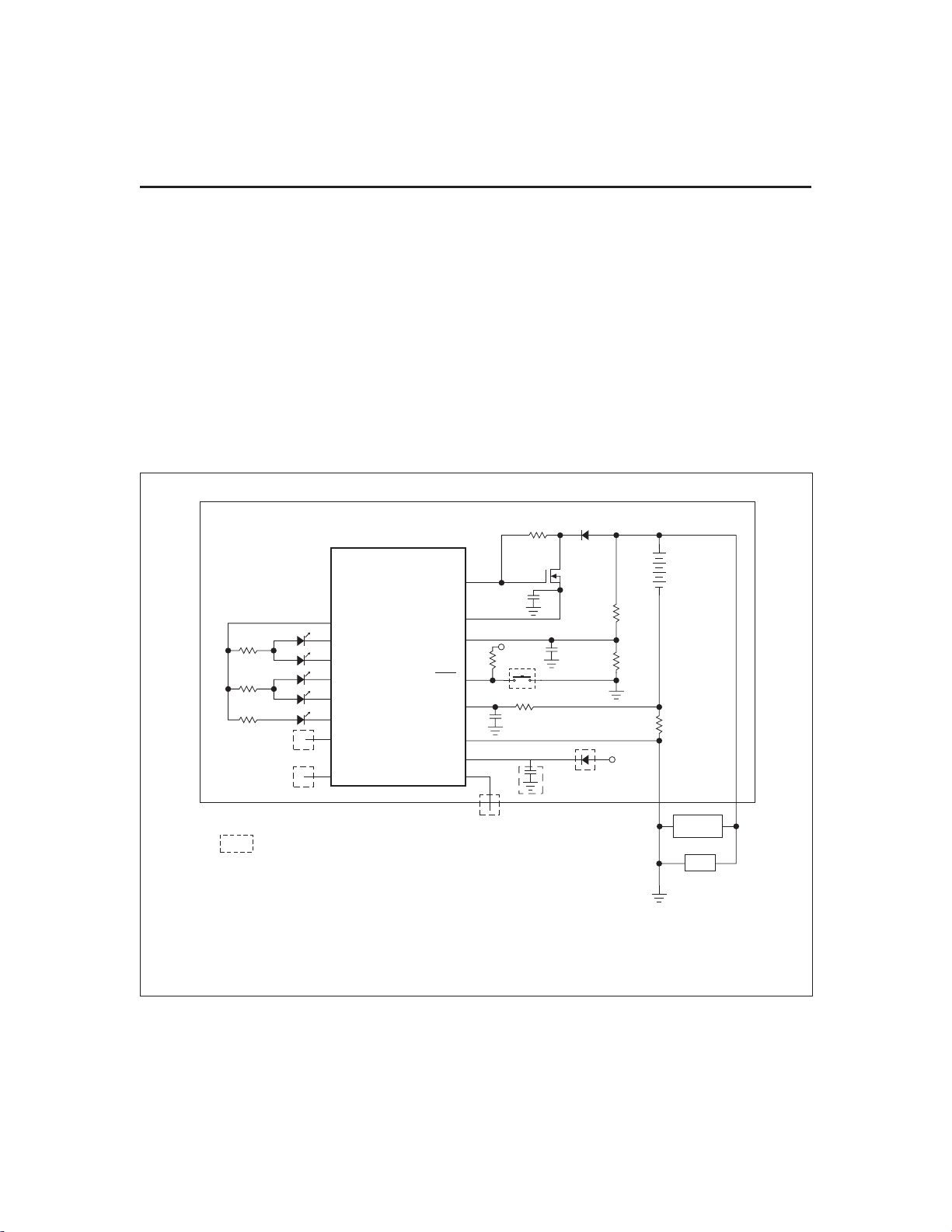
Figure 1 shows a typical battery pack application of the
bq2050H using the LED display capability as a charge-
state indicator. The bq2050H is configured to display
capacity in relative display mode. The relative display
mode uses the last measured discharge capacity of the
battery as the battery “full” reference. A push-button
display feature is available for momentarily enabling
the LED display.
-
The bq2050H monitors the charge and discharge cur
rents as a voltage across a sense resistor. (See R
ure 1.) A filter between the negative battery terminal
and the SR pin is required.
-
R
1
Q1
ZVNL110A
C1
RB
1
V
CC
100K
0.1µF
C2
RB
See note 4
2
R
S
in Fig
S
-
-
-
Notes:
1. Indicates optional.
2. Programming resistors and ESD-protection diodes are not shown.
3. RC on SR is required.
4. A series diode is required on RBI if the bottom series cell is used as the backup source.
If the cell is used, the backup capacitor is not required, and the anode is connected to the
positive terminal of the cell.
Figure 1. Battery Pack Application Diagram—LED Display
3
Charger
Load
FG2050H1.eps
Page 4

bq2050H
Voltage Thresholds
In conjunction with monitoring VSRfor charge/discharge
currents, the bq2050H monitors the battery potential
through the SB pin. The voltage is determined through
a resistor-divider network per the following equation:
RB1
RB2
4N=−1
where N is the number of cells, RB1 is connected to the
positive battery terminal, and RB2 is connected to the
negative battery terminal. The single-cell battery volt
age is monitored for the end-of-discharge voltage (EDV)
thresholds. The EDV threshold levels are used to deter
mine when the battery has reached an “empty” state.
The EDV thresholds for the bq2050H are programmable
with the default values fixed at:
EDV1 (first) = 0.76V
EDVF (final) = EDV1-0.025V = 0.735V
If V
is below either of the two EDV thresholds, the as
SB
sociated flag is latched and remains latched, independent of V
also available over the serial port.
, until the next valid charge. The VSBvalue is
SB
During discharge and charge, the bq2050H monitors
V
for various thresholds used to compensate the
SR
charge counter. EDV monitoring is disabled if the discharge rate is greater than 2C (OVLD Flag = 1) and re-
1
sumes
second after the rate falls below 2C.
2
RBI Input
The RBI input pin is intended to be used with a storage
capacitor or external supply to provide backup potential
to the internal bq2050H registers when V
3.0V. V
ing an external supply (such as the bottom series cell) as
is output on RBI when VCCis above 3.0V. If us
CC
drops below
CC
the backup source, an external diode is required for isola
tion.
Reset
The bq2050H can be reset by removing VCCand ground
ing the RBI pin for 15 seconds or by commands over the
serial port. The serial port reset command sequence re
quires writing 00h to register PPFC (address = 1Eh) and
then writing 00h to register LMD (address = 05h).
Temperature
The bq2050H internally determines the temperature in
10°C steps centered from approximately -35°C to +85°C.
The temperature steps are used to adapt charge and dis
charge rate compensations, self-discharge counting, and
available charge display translation. The temperature
range is available over the serial port in 10°C incre
ments as shown in the following table:
TMP (hex) Temperature Range
0x < -30°C
1x -30°C to -20°C
2x -20°C to -10°C
3x -10°C to 0°C
-
-
4x 0°C to 10°C
5x 10°C to 20°C
6x 20°C to 30°C
7x 30°C to 40°C
8x 40°C to 50°C
-
9x 50°C to 60°C
Ax 60°C to 70°C
Bx 70°C to 80°C
Cx > 80°C
Layout Considerations
The bq2050H measures the voltage differential between
the SR and V
pin) is greatly affected by PC board layout. For optimal
results, the PC board layout should follow the strict rule
of a single-point ground return. Sharing high-current
ground with small signal ground causes undesirable
noise on the small signal nodes. Additionally:
■
The capacitors (C1 and C2) should be placed as
close as possible to the V
-
respectively, and their paths to V
short as possible. A high-quality ceramic capacitor
-
of 0.1µF is recommended for V
■
The sense-resistor capacitor should be placed as close
as possible to the SR pin.
■
The sense resistor (RS) should be as close as possible to
the bq2050H.
-
-
pins. VOS(the offset voltage at the SR
SS
and SB pins,
CC
should be as
SS
.
CC
4
Page 5
bq2050H
Gas Gauge Operation
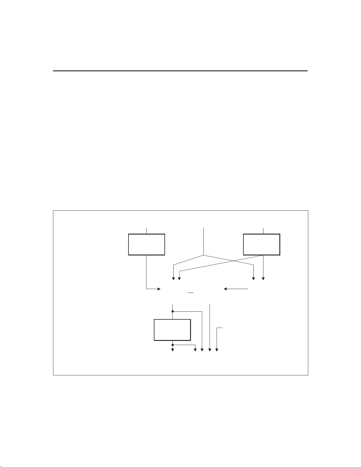
The operational overview diagram in Figure 2 illustrates
the operation of the bq2050H. The bq2050H accumu
lates a measure of charge and discharge currents, as
well as an estimation of self-discharge. The accumu
lated charge and discharge currents are adjusted for
temperature and rate to provide the indication of com
pensated available capacity to the host system or user.
The main counter, Nominal Available Capacity (NAC),
represents the available battery capacity at any given
time. Battery charging increments the NAC register,
while battery discharging and self-discharge decrement
the NAC register and increment the DCR (Discharge
Count Register).
The Discharge Count Register is used to update the Last
Measured Discharge (LMD) register only if a complete
battery discharge from full to empty occurs without any
partial battery charges. Therefore, the bq2050H adapts
its capacity determination based on the actual condi
tions of discharge.
Inputs
Charge
Current
Rate and
Temperature
Temperature
Compensation
Compensation
The battery's initial capacity equals the Programmed
Full Count (PFC) shown in Table 2. Until LMD is up
dated, NAC counts up to but not beyond this threshold
during subsequent charges. This approach allows the
gas gauge to be charger-independent and compatible
with any type of charge regime.
-
1. Last Measured Discharge (LMD) or learned
-
-
battery capacity:
LMD is the last measured discharge capacity of the
battery. On initialization (application of V
tery replacement), LMD = PFC. During subsequent
discharges, the LMD is updated with the latest
measured capacity in the Discharge Count Register
representing a discharge from full to below EDV1.
A qualified discharge is necessary for a capacity
transfer from the DCR to the LMD register. The
LMD also serves as the 100% reference threshold
used by the relative display mode.
Discharge
Current
Self-Discharge
Timer
Temperature
Compensation
CC
or bat
-
-
Main Counters
and Capacity
Reference (LMD)
Outputs
--
Nominal
+
Available
Charge
(NAC)
Rate and
Temperature
Compensation
Compensated
Available Charge
LED Display, etc.
<
Last
Measured
Discharged
(LMD)
Serial
Port
Figure 2. Operational Overview
5
+
Discharge
Count
Qualified
Transfer
Temperature Step,
Other Data
Register
(DCR)
FG2050H2.eps
+
Page 6

bq2050H
2. Programmed Full Count (PFC) or initial bat
tery capacity:
The initial LMD and gas gauge rate values are pro
grammed by using PROG
is configured for a given application by selecting a
–PROG4. The bq2050H
1
PFC value from Table 2. The correct PFC may be
determined by multiplying the rated battery capac
ity in mAh by the sense resistor value:
Battery capacity (mAh)*sense resistor (Ω) =
PFC (mVh)
Selecting a PFC slightly less than the rated capac
ity provides a conservative capacity reference until
-
Example: Selecting a PFC Value
Given:
Sense resistor = 0.05
Number of cells = 2
Capacity = 1000mAh, Li-Ion battery, coke-anode
-
Current range = 50mA to 1A
Relative display mode
Self-discharge =
NAC
Voltage drop over sense resistor = 2.5mV to 50mV
Nominal discharge voltage = 3.6V
Therefore:
-
1000mAh*0.05Ω= 50mVh
the bq2050H “learns” a new capacity reference.
Table 1. Self-Discharge and Capacity Compensation
Pin
Connection
H Coke anode/disabled LEDs disabled
Z Coke anode/
L Graphite anode/
PROG5Compensation/Self-Discharge
(See Tables 3 and 4)
NAC
512
NAC
512
LEDs on when charging
Table 2. bq2050H Programmed Full Count mVh, VSRGain Selections
Ω
per day @ 25°C
512
DISP
Display State
LEDs on for 4 s
Pro-
grammed
PROG
x
12
Full
Count
(PFC)
-- -
PROG
SCALE =
1/80
PROG
= L PROG4= Z or H
4
= H PROG3= Z PROG3= L PROG3= H PROG3= Z PROG3= L
3
SCALE =
1/160
SCALE =
1/320
SCALE =
1/640
SCALE =
1/1280
SCALE =
1/2560
Units
mVh/
count
H H 49152 614 307 154 76.8 38.4 19.2 mVh
H Z 45056 563 282 141 70.4 35.2 17.6 mVh
H L 40960 512 256 128 64.0 32.0 16.0 mVh
Z H 36864 461 230 115 57.6 28.8 14.4 mVh
Z Z 33792 422 211 106 53.0 26.4 13.2 mVh
Z L 30720 384 192 96.0 48.0 24.0 12.0 mVh
L H 27648 346 173 86.4 43.2 21.6 10.8 mVh
L Z 25600 320 160 80.0 40.0 20.0 10.0 mVh
L L 22528 282 141 70.4 35.2 17.6 8.8 mVh
V
equivalent to 2
SR
counts/s (nom.)
90 45 22.5 11.25 5.6 2.8 mV
6
Page 7

bq2050H
Select:
PFC = 30720 counts or 48mVh
= float
PROG
1
PROG
= low
2
PROG
= high
3
PROG
= float
4
PROG
= float
5
The initial full battery capacity is 48mVh (960mAh)
until the bq2050H “learns” a new capacity with a
qualified discharge from full to EDV1.
3. Nominal Available Capacity (NAC):
NAC counts up during charge to a maximum value
of LMD and down during discharge and self-dis
charge to 0. NAC is reset to 0 on initialization and
on the first valid charge following discharge to
EDV1. To prevent overstatement of charge during
periods of overcharge, NAC stops incrementing
when NAC = LMD.
4. Discharge Count Register (DCR):
The DCR counts up during discharge independent
of NAC and could continue increasing after NAC
has decremented to 0. Prior to NAC = 0 (empty
battery), both discharge and self-discharge increment the DCR. After NAC = 0, only discharge
increments the DCR. The DCR resets to 0 when
NAC = LMD. The DCR does not roll over but stops
counting when it reaches FFh.
The DCR value becomes the new LMD value on the
first charge after a valid discharge to V
the following conditions are met:
■
No valid charge initiations (charges greater than
2 NAC updates where V
during the period between NAC = LMD and EDV1.
■
The self-discharge is less than 6% of NAC.
■
The temperature is≥0°C when the EDV1 level
SRO>VSRQ
is reached during discharge.
■
VDQ is set
The valid discharge flag (VDQ) indicates whether
the present discharge is valid for LMD update. If
the DCR update value is less than 0.94 ∗ LMD, LMD
will only be modified by 0.94 ∗ LMD. This prevents
invalid DCR values from corrupting LMD.
5. Scaled Available Energy (SAE):
SAE is useful in determining the available energy
within the battery, and may provide a more useful
capacity reference in battery chemistries with
sloped voltage profiles during discharge. SAE may
be converted to an mWh value using the following
formula:
if all
EDV1
) occurred
E(mWh) =
(SAEH SAEL)∗+ ∗256
12. ∗∗
SCALE (R + R )
RR
B1 B2
SB2
∗
where RB1,RB2, and RSare resistor values in
ohms, as shown in Figure 1. SCALE is the selected
scale from Table 2.
6. Compensated Available Capacity (CACT)
CACT counts similarly to NAC, but contains the available
capacity compensated for discharge rate and temperature.
Charge Counting
Charge activity is detected based on a positive voltage
-
on the SR input. If charge activity is detected, the
bq2050H increments NAC at a rate proportional to V
and, if enabled, activates an LED display.
The bq2050H counts charge activity when the voltage at
theSRinput(V
threshold (V
has been updated twice without discharging or reaching
SRQ
) exceeds the minimum charge
SRO
). A valid charge is detected when NAC
the digital magnitude filter time-out. Once a valid
charge is detected, charge counting continues until V
including offset, falls below V
SRQ
.
Discharge Counting
Discharge activity is detected based on a negative voltage on the SR input. All discharge counts where V
is less than the minimum discharge threshold (V
cause the NAC register to decrement and the DCR to
increment.
Self-Discharge Counting
The bq2050H continuously decrements NAC and incre
ments DCR for self-discharge based on time and tempera
ture.
Charge/Discharge Current
The bq2050H current-scale registers, VSRH and VSRL,
can be used to determine the battery charge or dis
charge current. See the Current Scale Register descrip
tion for details.
Count Compensations
Compensated Available Capacity
Compensated Available Capacity compensation is based
on the rate of discharge, temperature, and negative
electrode type. Tables 3A and 3B outline the correction
factor typically used for graphite-anode Li-Ion batteries,
and Tables 4A and 4B outline the factors typically used for
coke-anode Li-Ion batteries. The compensation factor is
applied to NAC to derive the CACD and CACT values.
SR
SRO
SRD
SR
,
)
-
-
-
-
7
Page 8

bq2050H
Table 3A. Graphite Anode
Approximate Discharge
Rate
0.5C 0
<
0.5C
≥
Table 3B. Graphite Anode
Temperature
10°C 0
≥
0°C to 10°C
-20°C to 0°C
-20°C
≤
Table 4A. Coke Anode
Approximate Discharge
Rate
0.5C 0
<
0.5C
≥
Table 4B. Coke Anode
Temperature
10°C 0
≥
0°C to 10°C
-20°C to 0°C
-20°C
≤
Available Capacity
Reduction
0.05 ∗ LMD
Available Capacity
Reduction
0.05 ∗ LMD
0.15 ∗ LMD
0.37 ∗ LMD
Available Capacity
Reduction
0.10 ∗ LMD
Available Capacity
Reduction
0.10 ∗ LMD
0.30 ∗ LMD
0.60 ∗ LMD
Charge Compensation
The bq2050H also monitors temperature during charge.
If the temperature is <0°C, NAC will only increment up
to 0.94 * LMD, inhibiting VDQ from being set. This
keeps a “learn” cycle from occurring when the battery is
charged at very low temperatures. If the temperature
rises above 0°C, NAC will be allowed to count up to NAC
= LMD.
Self-Discharge Compensation
The self-discharge compensation is programmed for a
nominal rate of
NAC is reduced for a battery within the 20–30°C tem
perature range. This rate varies across 8 ranges from
<10°C to >70°C, as shown in Table 5.
1
∗ NAC per day. This is the rate that
512
Table 5. Self-Discharge Compensation
Typical Rate
Temperature Range
< 10°C
10–20°C
20–30°C
30–40°C
40–50°C
50–60°C
60–70°C
> 70°C
Self-discharge may be disabled by connecting PROG
PROG
= Z or L
5
NAC
NAC
NAC
NAC
NAC
NAC
NAC
NAC
2048
1024
512
256
128
64
32
16
=H.
5
Digital Magnitude Filter
The bq2050H has a digital filter to eliminate charge and
discharge counting below a set threshold. The minimum
charge (V
) and discharge (V
SRQ
) threshold for the
SRD
bq2050H is 250µV.
Pack Protection Supervision
-
The CACD value is the available charge compensated
for the rate of discharge. At high discharge rates, CACD
is reduced. The reduction is maintained until a valid
charge is detected. The CACT value is the available
charge compensated for the rate of discharge and tem
perature. The CACT value is used to drive the LED dis
play.
The bq2050H can monitor the charge FET in a Li-Ion
pack protector circuit as shown in Figure 3. If the bat
tery voltage is too high or the temperature is out of the
0—60°C range, the bq2050H disables the charge FET
with the CFC output, which turns off the charge to the
pack.
-
-
The PSTAT input is used to monitor the protector state. If
PSTAT is above 2.5V, bit 5 of FLGS1 is set to 1. If PSTAT
is below 0.5V, bit 5 of FLGS1 is cleared to zero. Using this
input, the system can monitor the state of the charge con
8
-
-
Page 9

Table 6. bq2050H Current-Sensing Errors
Symbol Parameter Typical Maximum Units Notes
INL
INR
Integrated non-linearity
error
Integrated nonrepeatability error
2
±
1
±
4
±
2
±
Add 0.1% per °C above or below 25°C
%
and 1% per volt above or below 4.25V.
Measurement repeatability given
%
similar operating conditions.
bq2050H
trol FET signal and can quickly determine if the protector
circuit is operating properly during charge.
Register 15h, NMCV, is used to set the maximum bat
tery voltage for the battery stack. If V
battery temperature is < 0°Cor>60°C, then CFC is
driven low.
> NMCV or the
SB
Error Summary
Capacity Inaccurate
The LMD is susceptible to error on initialization or if no
updates occur. On initialization, the LMD value includes the error between the programmed full capacity
and the actual capacity. This error is present until a
valid discharge occurs and LMD is updated (see the
DCR description). The other cause of LMD error is battery wear-out. As the battery ages, the measured capacity must be adjusted to account for changes in actual
battery capacity.
Discharge
Control
A Capacity Inaccurate counter (CPI) is maintained and
incremented each time a valid charge occurs (qualified
by NAC; see the CPI register description). It is reset
-
whenever LMD is updated from the DCR. The counter
does not wrap around but stops counting at 255. The ca
pacity inaccurate flag (CI) is set if LMD has not been
updated following 64 valid charges.
Current-Sensing Error
Table 6 shows the non-linearity and non-repeatability
errors associated with the bq2050H current sensing.
Table 7 illustrates the current-sensing error as a function of V
charge counts to the NAC register when V
tween V
P S TAT
bq2050H
. A digital filter prevents charge and dis-
OS
SRQ
and V
SRD
R
.
Charger
LOAD
SRO
-
is be-
Charge
Control
R
S
CFC
SR
V
SS
FG2050H3.eps
Figure 3. bq2050H Pack Supervision
9
Page 10

bq2050H
Table 7. VOS-Related Current Sense Error
(Current = 1A)
V
OS
(µV)
50 0.25 0.10 0.05 %
100 0.50 0.20 0.10 %
150 0.75 0.30 0.15 %
180 0.90 0.36 0.18 %
20 50 100
Sense Resistor
mΩ
Communicating With the bq2050H
The bq2050H includes a simple single-pin (HDQ plus return)
serial data interface. A host processor uses the interface to
access various bq2050H registers. Battery characteristics
may be easily monitored by adding a single contact to the
battery pack. The open-drain HDQ pin on the bq2050H
should be pulled up by the host system, or may be left float
ing if the serial interface is not used.
The interface uses a command-based protocol, where the
host processor sends a command byte to the bq2050H.
The command directs the bq2050H to either store the
next eight bits of data received to a register specified by
the command byte or output the eight bits of data specified by the command byte. (See Figure 4.)
The communication protocol is asynchronous return-toone. Command and data bytes consist of a stream of
eight bits that have a maximum transmission rate of
5K bits/sec. The least-significant bit of a command or
data byte is transmitted first. The protocol is simple
enough that it can be implemented by most host proces
sors using either polled or interrupt processing. Data in
put from the bq2050H may be sampled using the pulsewidth capture timers available on some microcontrollers.
should be held for a period, t
bq2050H to sample the data bit.
The final section is used to stop the transmission by re
turning the HDQ pin to a logic-high state by at least a
period, t
munication. The final logic-high state should be until a
period t
transmission was stopped properly. The timings for data
and break communication are given in the serial com
munication timing specification and illustration sec
tions.
Communication with the bq2050H is always performed
with the least-significant bit being transmitted first. Fig
ure 5 shows an example of a communication sequence to
read the bq2050H NACH register.
, after the negative edge used to start com
SSU;B
, to allow time to ensure that the bit
CYCH;B
, to allow the host or
DH;DV
bq2050H Command Code and
Registers
The bq2050H status registers are listed in Table 8 and de
scribed below. All registers are Read/Write in the bq2050H.
Caution: When writing to bq2050H registers ensure
that proper data is written. A write-verify read is recommended.
Command Code
The bq2050H latches the command code when eight
valid command bits have been received by the bq2050H.
The command code contains two fields:
■
W/R bit
■
Command address
-
The W/R
-
the received command is for a read or a write function.
The W/R
bit of the command code is used to select whether
values are:
-
-
-
-
-
-
If a communication error occurs (e.g., t
the bq2050H should be sent a BREAK to reinitiate the
serial interface. A BREAK is detected when the HDQ
pin is driven to a logic-low state for a time, t
The HDQ pin should then be returned to its normal
ready-high logic state for a time, t
now ready to receive a command from the host proces
sor.
The return-to-one data bit frame consists of three dis
tinct sections. The first section is used to start the
transmission by either the host or the bq2050H taking
the HDQ pin to a logic-low state for a period, t
The next section is the actual data transmission, where
the data should be valid by a period, t
negative edge used to start communication. The data
. The bq2050H is
BR
CYCB
DSU;B
> 250µs),
or greater.
B
STRH;B
, after the
Command Code Bits
7654 3 2 1 0
W/R
Where W/R
-
-
.
The lower seven-bit field of the command code contains
the address portion of the register to be accessed.
- -- - - - -
is:
0 The bq2050H outputs the requested register
contents specified by the address portion of com
mand code.
1 The following eight bits should be written to the
register specified by the address portion of com
mand code.
10
-
-
Page 11

bq2050H
Break
Send Host to bq-HDQ
CDMR
LSB
Bit0
Start-bit
Address
Address-Bit/
Data-Bit
Send Host to bq-HDQ or
Receive from bq-HDQ
Stop-Bit
TD201807.eps
Figure 4. bq2050H Communication Example
Data
R/W
MSB
Bit7
t
RSPS
t
RR
Written by Host to bq2050H
CMDR = 03h
Received by Host to bq2050H
NACH = 65h
LSB MSB LSB MSB
Break 0 0 0000 1010011
110
HDQ
t
RSPS
Figure 5. Typical Communication With the bq2050H
11
TD2050H2.eps
Page 12

bq2050H
Table 8. bq2050H Command and Status Registers
Loc.
Read/
(hex)
Symbol Register Name
FLGS1
TMP Temperature register 02h R TMP3 TMP2 TMP1 TMP0 GG3 GG2 GG1 GG0
NACH
NACL
BATID
LMD
FLGS2
PPD
PPU
CPI
VSB
VTS
CACT
CACD
SAEH
SAEL
RCAC Relative CAC 11h R - RCAC6 RCAC5 RCAC4 RCAC3 RCAC2 RCAC1 RCAC0
VSRH Current scale high 12h R VSRH7 VSRH6 VSRH5 VSRH4 VSRH3 VSRH2 VSRH1 VSRH0
VSRL Current scale low 13h R VSRL7 VSRL6 VSRL5 VSRL4 VSRL3 VSRL2 VSRL1 VSRL0
NMCV Maximum cell voltage 15h R/W NMCV7 NMCV6 NMCV5 NMCV4 NMCV3 NMCV2 NMCV1 NMCV0
DCR Discharge register 18h R/W DCR7 DCR6 DCR5 DCR4 DCR3 DCR2 DCR1 DCR0
PPFC Program pin data 1eh R/W RSVD RSVD RSVD RSVD RSVD RSVD RSVD RSVD
INTSS V
RST Reset register 39h R/W RST 0 0 0 0 0 0 0
HEXFF Check register 3fh R/W 1 1 1 1 1 1 1 1
Notes: RSVD = reserved.
Primary status flags
register
Nominal available capac
ity high byte register
Nominal available
capacity low byte register
Battery identification
register
Last measured
discharge register
Secondary status flags
register
Program pin pull-down
register
Program pin pull-up
register
Capacity
inaccurate count register
Battery voltage
register
End-of-discharge threshold select register
Temperature and Discharge Rate compensated
available capacity
Discharge Rate com
pensated available
capacity
Scaled available energy
high byte register
Scaled available energy
low byte register
Interrupt 38h R RSVD RSVD RSVD RSVD DCHGI RSVD RSVD CHGI
OS
All other registers not documented are reserved.
-
-
Write
01h R CHGS BRP PSTAT CI VDQ 1 EDV1 EDVF
03h R/W NACH7 NACH6 NACH5 NACH4 NACH3 NACH2 NACH1 NACH0
17h R/W NACL7 NACL6 NACL5 NACL4 NACL3 NACL2 NACL1 NACL0
04h R/W BATID7 BATID6 BATID5 BATID4 BATID3 BATID2 BATID1 BATID0
05h R/W LMD7 LMD6 LMD5 LMD4 LMD3 LMD2 LMD1 LMD0
06h R RSVD DR2 DR1 DR0 ENINT VQ RSVD OVLD
07h R RSVD RSVD RSVD PPD5 PPD4 PPD3 PPD2 PPD1
08h R RSVD RSVD RSVD PPU5 PPU4 PPU3 PPU2 PPU1
09h R/W CPI7 CPI6 CPI5 CPI4 CPI3 CPI2 CPI1 CPI0
0bh R VSB7 VSB6 VSB5 VSB4 VSB3 VSB2 VSB1 VSB0
0ch R/W VTS7 VTS6 VTS5 VTS4 VTS3 VTS2 VTS1 VTS0
0dh R/W CACT7 CACT6 CACT5 CACT4 CACT3 CACT2 CACT1 CACT0
0eh R/W CACD7 CACD6 CACD5 CACD4 CACD3 CACD2 CACD1 CACD0
0fh R SAEH7 SAEH6 SAEH5 SAEH4 SAEH3 SAEH2 SAEH1 SAEH0
10h R SAEL7 SAEL6 SAEL5 SAEL4 SAEL3 SAEL2 SAEL1 SAEL0
Control Field
7(MSB) 6 5 4 3 2 1 0(LSB)
12
Page 13

bq2050H
Command Code Bits
765 4 3 2 1 0
- AD6 AD5 AD4 AD3 AD2 AD1
AD0
(LSB)
Primary Status Flags Register (FLGS1)
The FLGS1 register (address = 01h) contains the pri
mary bq2050H flags.
The charge status flag (CHGS) is asserted when a
valid charge rate is detected. Charge rate is deemed
valid when V
discharge activity clears CHGS.
SRO>VSRQ
The CHGS values are:
76543 2 1 0
CHGS - -- - - - -
Where CHGS is:
0 Either discharge activity detected or V
≤ V
SRQ
1V
SRO
> V
SRQ
The battery replaced flag (BRP) is asserted whenever
the bq2050H is reset either by application of V
serial port command. BRP is reset when either a valid
charge action increments NAC to be equal to LMD, or a
valid charge action is detected after the EDV1 flag is as
serted. BRP = 1 signifies that the device has been reset.
The BRP values are:
76543 2 1 0
- BRP - - - - - -
Where BRP is:
0 Battery is charged until NAC = LMD or dis
charged until the EDV1 flag is asserted
1 bq2050H is reset
The protector status flag (PSTAT) provides information
on the state of the overvoltage protector within the LiIon battery pack. The PSTAT flag is asserted whenever
this input is high and is cleared when the input is low.
.AV
SRO
FLGS1 Bits
FLGS1 Bits
of less than V
SRO
CC
SRQ
or by a
-
or
The PSTAT values are:
FLGS1 Bits
76 5 43210
--PSTAT-----
Where PSTAT is:
0 PSTAT input is low (PSTAT < 0.5V)
-
1 PSTAT input is high (PSTAT > 2.5V)
The capacity inaccurate flag (CI) is used to warn the
user that the battery has been charged a substantial
number of times since LMD has been updated. The CI
flag is asserted on the 64th charge after the last LMD
update or when the bq2050H is reset. The flag is cleared
after an LMD update.
The CI values are:
FLGS1 Bits
7654 3 2 1 0
---CI- - - -
Where CI is:
0 When LMD is updated with a valid full dis-
charge
1 After the 64th valid charge action with no
LMD updates or the bq2050H is reset
The valid discharge flag (VDQ) is asserted when the
bq2050H is discharged from NAC=LMD. The flag re
mains set until either LMD is updated or one of three
actions that can clear VDQ occurs:
■
When NAC has been reduced by more than 6%
because of self-discharge since VDQ was set.
■
A valid charge action sustained at V
at least 2 NAC updates.
■
The EDV1 flag was set at a temperature below 0°C
SRO>VSRQ
The VDQ values are:
FLGS1 Bits
76543 2 1 0
- - - - VDQ - - -
Where VDQ is:
0 Self-discharge of 6% of NAC, valid charge
action detected, EDV1 asserted with the
temperature less than 0°C, or reset
1 On first discharge after NAC = LMD
-
for
13
Page 14

bq2050H
The first end-of-discharge warning flag (EDV1)
warns the user that the battery is almost empty. The
first segment pin, SEG
the display is enabled once EDV1 is asserted, which
, is modulated at a 4Hz rate if
1
should warn the user that loss of battery power is immi
nent. The EDV1 flag is latched until a valid charge has
been detected. The EDV1 threshold is externally con
trolled via the VTS register (see Voltage Threshold Reg
ister).
The EDV1 values are:
FLGS1 Bits
7654 3 2 1 0
- - - - - - EDV1 -
Where EDV1 is:
0 Valid charge action detected, V
SB
V
≥
TS
1VSB<VTSproviding that the discharge rate
is<2C
The final end-of-discharge warning flag (EDVF) flag
is used to warn that battery power is at a failure condition. All segment drivers are turned off. The EDVF flag
is latched until a valid charge has been detected. The
EDVF threshold is set 25mV below the EDV1 threshold.
The EDVF values are:
FLGS1 Bits
7654 3 2 1 0
---- - - -EDVF
Where EDVF is:
0 Valid charge action detected,V
1V
< (VTS-25mV) providing the discharge
SB
rate is < 2C
SB
- 25mV)
(V
≥
TS
Temperature Register (TMP)
The TMP register (address=02h) contains the battery
temperature.
The bq2050H contains an internal temperature sensor.
The temperature is used to set charge and discharge ef
ficiency factors as well as to adjust the self-discharge co
efficient. The temperature register contents may be
translated as shown in Table 9.
TMP Temperature Bits
76543210
TMP3 TMP2 TMP1 TMP0 - - - -
The bq2050H calculates the gas gauge bits, GG3-GG0 as a
function of CACT and LMD. The results of the calculation
give available capacity in
-
76 5 4 321 0
-
-
- - - - GG3 GG2 GG1 GG0
1
increments from 0 to
16
TMP Gas Gauge Bits
Table 9. Temperature Register
TMP3 TMP2 TMP1 TMP0 Temperature
0000 T < -30°C
0001-30°C < T < -20°C
0010-20°C < T < -10°C
0011-10°C < T < 0°C
01000°C < T < 10°C
010110°C < T < 20°C
011020°C < T < 30°C
011130°C < T < 40°C
100040°C < T < 50°C
100150°C < T < 60°C
101060°C < T < 70°C
101170°C < T < 80°C
1100 T > 80°C
Nominal Available Capacity Registers
(NACH/NACL)
The NACH high-byte register (address=03h) and the
NACL low-byte register (address=17h) are the main gas
gauging registers for the bq2050H. The NAC registers are
incremented during charge actions and decremented dur
ing discharge and self-discharge actions. NACH and
NACL are set to 0 during a bq2050H reset.
Writing to the NAC registers affects the available charge
counts and, therefore, affects the bq2050H gas gauge opera
tion. Do not write the NAC registers to a value greater than
LMD.
Battery Identification Register (BATID)
The BATID register (address=04h) is available for use
by the system to determine the type of battery pack.
The BATID contents are retained as long as V
greater than 2V. The contents of BATID have no effect
on the operation of the bq2050H. There is no default
setting for this register.
15
.
16
-
-
is
RBI
14
Page 15

bq2050H
Last Measured Discharge Register (LMD)
LMD is the register (address=05h) that the bq2050H
uses as a measured full reference. The bq2050H adjusts
LMD based on the measured discharge capacity of the
battery from full to empty. In this way the bq2050H up
dates the capacity of the battery. LMD is set to PFC
during a bq2050H reset.
LMD is set to DCR upon the first valid charge after EDV
is set if VDQ is set.
If DCR < 0.94 LMD, then LMD is set to 0.94 ∗ LMD.
Secondary Status Flags Register (FLGS2)
The FLGS2 register (address=06h) contains the secon
dary bq2050H flags.
Bit 7 and bit 1 of FLGS2 are reserved. Do not write to
these bits.
The discharge rate flags, DR2–0,are bits 6–4.
FLGS2 Bits
7 6 5 4 3210
- DR2 DR1 DR0 - - -
They are used to determine the current discharge regime as follows:
DR2 DR1 DR0 Discharge Rate
0 0 0 DRATE<0.5C
0 0 1 0.5C≤DRATE<2C
0 1 0 2C < DRATE
The enable interrupt flag (ENINT) is a test bit used to
determine V
state of this bit will vary and should be ignored by the
system.
76543210
- - - - ENINT - -
activity sensed by the bq2050H. The
SR
FLGS2 Bits
Where VQ is:
0 Valid charge action not detected between a
discharge from NAC = LMD and EDV1
1 Valid charge action detected
The overload flag (OVLD) is asserted when a discharge
rate in excess of 2C is detected. OVLD remains asserted
as long as the condition persists and is cleared 0.5 sec
onds after the rate drops below 2C. The overload condi
tion is used to stop sampling of the battery terminal char
acteristics for end-of-discharge determination.
FLGS2 Bits
76543 2 1 0
-
- - - - - - - OVLD
Program Pin Pull-Down Register (PPD)
The PPD register (address=07h) contains some of the pro
gramming pin information for the bq2050H. The segment
drivers, SEG
tion, PPD
tor has been detected on its corresponding segment driver.
For example, if SEG
the contents of PPD are xxx01001.
, have a corresponding PPD register loca
1–5
. A given location is set if a pull-down resis-
1–5
and SEG4have pull-down resistors,
1
Program Pin Pull-Up Register (PPU)
The PPU register (address=08h) contains the rest of the
programming pin information for the bq2050H. The segment drivers, SEG
location, PPU
tor has been detected on its corresponding segment driver.
For example, if SEG
contents of PPU are xxx10100.
7 6 5 43210
RSVD RSVD RSVD PPU
RSVD RSVD RSVD PPD5PPD4PPD3PPD2PPD
, have a corresponding PPU register
1–5
. A given location is set if a pull-up resis-
1–5
and SEG5have pull-up resistors, the
3
PPD/PPU Bits
PPU4PPU3PPU2PPU
5
-
-
-
-
-
1
1
The valid charge flag (VQ), bit 2 of FLGS2, is used to
indicate whether the bq2050H recognizes a valid charge
condition. This bit is reset on the first discharge after
NAC = LMD.
The VQ values are:
FLGS2 Bits
76543210
-----VQ-
Capacity Inaccurate Count Register (CPI)
The CPI register (address=09h) is used to indicate the
number of times a battery has been charged without an
LMD update. Because the capacity of a rechargeable
battery varies with age and operating conditions, the
bq2050H adapts to the changing capacity over time. A
complete discharge from full (NAC=LMD) to empty
(EDV1=1) is required to perform an LMD update assum
ing there have been no intervening valid charges, the
temperature is greater than or equal to 0°C, and there
has been no more than a 6% self-discharge reduction.
15
-
Page 16

bq2050H
The CPI register is incremented every time a valid
charge is detected. When NAC > 0.94*LMD, however,
the CPI register increments on the first valid charge;
CPI does not increment again for a valid charge until
NAC < 0.94*LMD. This prevents continuous trickle
charging from incrementing CPI if self-discharge decre
ments NAC. The CPI register increments to 255 with
out rolling over. When the contents of CPI are incre
mented to 64, the capacity inaccurate flag, CI, is as
serted in the FLGS1 register. The CPI register is reset
whenever an update of the LMD register is performed,
and the CI flag is also cleared.
Battery Voltage Register (VSB)
The battery voltage register is used to read the single-cell
battery voltage on the SB pin. The VSB register (address
= 0Bh) is updated approximately once per second with the
present value of the battery voltage.
V
= 1.2V*(VSB/256).
SB
VSB Register Bits
76543210
VSB7 VSB6 VSB5 VSB4 VSB3 VSB2 VSB1 VSB0
Voltage Threshold Register (VTS)
The end-of-discharge threshold voltages (EDV1 and
EDVF) can be set using the VTS register (address =
0Ch). The VTS register sets the EDV1 trip point. EDVF
is set 25mV below EDV1. The default value in the VTS
register is A2h, representing EDV1 = 0.76V and EDVF =
0.735V. EDV1 = 1.2V*(VTS/256).
VTS Register Bits
76543210
VTS7 VTS6 VTS5 VTS4 VTS3 VTS2 VTS1 VTS0
Scaled Available Energy Registers
(SAEH/SAEL)
The SAEH high-byte register (address = 0Fh) and the
SAEL low-byte register (address = 10h) are used to scale
-
battery voltage and CACT to a value that can be trans
-
lated to watt-hours remaining under the present condi
-
tions.
-
Relative CAC Register (RCAC)
The RCAC register (address = 11h) provides the relative
battery state-of-charge by dividing CACT by LMD.
RCAC varies from 0 to 64h representing relative stateof-charge from 0 to 100%.
Current Scale Register (VSRH/VSRL)
The VSRH register (address = 12h) and the VSRL regis
ter (address = 13h) report the average signal across the
SR and V
pair every 22.5s. V
form a 16-bit signed integer value representing the av
erage current during this time. The battery pack current
can be calculated from:
I(mA) = (V
where:
R
S
V
SRH
V
SRL
The bq2050H indicates an average discharge current
with a “1” in the MSB position of the VSRH register. To
calculate discharge current, use the 2’s complement if
the concatenated register contents in the above equa
tion.
pins. The bq2050H updates this register
SS
SRH
= sense resistor value in Ω.
= high-byte value of battery current
= low-byte value of battery current
(high-byte) and V
SRH
∗ 256 + V
SRL
)/(8 ∗RS)
SRL
-
-
-
(low-byte)
-
-
Compensated Available Charge Registers
(CACT/CACD)
The CACD register (address = 0Eh) contains the NAC
value compensated for discharge rate. This is a mono
tonicly decreasing value during discharge. If the dis
charge rate is > 0.5C then this value is lower than NAC.
CACD is updated only when the discharge rate compen
sated NAC value is a lower value than CACD during
discharge. During charge, CACD is continuously up
dated with the NAC value.
The CACT register (address = 0Dh) contains the CACD
value compensated for temperature. CACT will contain
a value lower than CACD when the battery temperature
is below 10°C. The CACT value is also used in calculat
ing the LED display pattern.
-
-
-
-
-
16
Page 17

bq2050H
Maximum Cell Voltage Register (NMCV)
The NMCV register (address 15h) is used to set the
maximum battery pack voltage for control of the CFC
pin. If desired, the system can write a value to NMCV to
enable CFC to go low if V
may be useful as a secondary protection of the Li-Ion
battery pack. NMCV should be set to the following
equation:
NMCV = 2s complement of
Where:
MCV = maximum desired battery stack voltage.
NMCV = set to 00h on power up or reset and
should be programmed to the desired value
by the host system.
exceeds this value. This
SB
256 MCV RB2
∗∗
1.2 RB1 + RB2
∗
()
Discharge Count Register (DCR)
The DCR register (address = 18h) stores the high-byte of
the discharge count. DCR is reset to zero at the start of
a valid discharge cycle and can count to a maximum of
FFh. DCR will not increment if EDV1 = 1 and will not
roll over from FFh.
Program Pin Full Count (PPFC)
The PPFC register contains information concerning the
program pin configuration. This information is used to
determine the data integrity of the bq2050H. The only
approved user application for this register is to
write a zero to this register as part of a reset re
quest.
Voltage Offset (VOS) Interrupt (INTSS)
The INTSS register (address = 38h) is useful during in
tial characterization of bq2050H designs. When the
bq2050H counts a charge pulse, CHGI (bit 0) will be set
to 1. When the bq2050H counts a discharge pulse,
DCHGI (bit 3) will be set to 1. All other locations in the
INTSS register are reserved.
Reset Register (RST)
The reset register (address = 39h) provides an alternate
means of initializing the bq2050H via software. Since this
register contains device test bits, it is recommended to use
the PPFC and LMD registers to reset the bq2050H. Set
ting any bits in the reset register is not allowed and
will result in improper bq2050H operation. The rec
ommended reset method for the bq2050H is :
■
Write PPFC to zero
■
Write LMD to zero
After these operations, a software reset will occur.
Resetting the bq2050H sets the following:
LMD = PFC
■
CPI, VDQ, RCAC, NACH/L, CACH/L, SAEH/L,
■
NMCV = 0
CI and BRP = 1
■
Check Register (HEXFF)
The HEXFF register (address = 3F) is useful in de
terming if the device is a bq2050H or a bq2050. This
register is always set to FFh for the bq2050H. The
bq2050 returns data other than FFh.
Display
The bq2050H can directly display capacity information
using low-power LEDs. If LEDs are used, the program
pins should be resistively tied to V
gram high or program low, respectively.
The bq2050H displays the battery charge state in relative
mode. In relative mode, the battery charge is represented
as a percentage of the LMD. Each LED segment represents 20% of the LMD.
The capacity display is also adjusted for the present battery
temperature and discharge rate. The temperature adjustment reflects the available capacity at a given temperature
but does not affect the NAC register. The temperature adjustments are detailed in the CACT and CACD register descriptions.
-
When DISP
tive. When DISP
tive whenever the bq2050H detects a charge in progress
V
SRO>VSRQ
come active for a period of four seconds,±0.5 seconds.
The segment outputs are modulated as two banks, with seg
ments 1, 3, and 5 alternating with segments 2 and 4. The
segment outputs are modulated at approximately 100Hz with
each segment bank active for 30% of the period.
SEG
tected to be below V
battery condition. V
the display output.
-
Microregulator
A micropower source for the bq2050H can be inexpen
sively built using a FET and an external resistor. (See
Figure 1.)
is tied to VCC, the SEG
is left floating, the display becomes ac
. When pulled low, the segment outputs be
blinks at a 4Hz rate whenever VSBhas been de
1
(EDV1 = 1), indicating a low-
EDV1
below V
SB
EDVF
or VSSfor a pro
CC
outputs are inac
1–5
(EDVF = 1) disables
-
-
-
-
-
-
-
-
17
Page 18

bq2050H
Absolute Maximum Ratings
Symbol Parameter Minimum Maximum Unit Notes
V
CC
All other pins Relative to V
REF Relative to V
V
SR
T
OPR
Relative to V
Relative to V
SS
SS
SS
SS
Operating temperature 0 +70 °C Commercial
Note: Permanent device damage may occur if Absolute Maximum Ratings are exceeded. Functional
operation should be limited to the Recommended DC Operating Conditions detailed in this data sheet.
Exposure to conditions beyond the operational limits for extended periods of time may affect device reli
ability.
-0.3 +7.0 V
-0.3 +7.0 V
-0.3 +8.5 V Current limited by R1 (see Figure 1)
100kΩseries resistor should be used
-0.3 Vcc+0.7 V
to protect SR in case of a shorted bat
tery.
-
-
DC Voltage Thresholds (T
A=TOPR
; V = 3.0 to 6.5V)
Symbol Parameter Minimum Typical Maximum Unit Notes
V
V
V
V
V
V
EDV1
EDVF
SRO
SRQ
SRD
MCV
First empty warning 0.73 0.76 0.79 V SB, default
Final empty warning V
EDV1
- 0.035 V
EDV1
- 0.025 V
- 0.015 V SB, default
EDV1
SR sense range -300 - +500 mV SR, VSR+V
Valid charge 250 - -
Valid discharge - - -250
VVSR+VOS(see note)
µ
VVSR+VOS(see note)
µ
Maximum SB voltage 1.10 1.12 1.15 V SB pin
OS
Note: VOSis affected by PC board layout. Proper layout guidelines should be followed for optimal performance.
See “Layout Considerations.”
18
Page 19

bq2050H
DC Electrical Characteristics (T
=T
OPR
)
A
Symbol Parameter Minimum Typical Maximum Unit Notes
excursion from < 2.0V to
V
V
CC
V
OS
V
REF
R
REF
I
CC
V
SB
R
SBmax
I
DISP
I
LCOM
I
RBI
R
HDQ
R
SR
V
IHPFC
V
ILPFC
V
IZPFC
V
OLSL
V
OLSH
V
OHML
V
OHMH
I
OLS
I
OL
V
OL
V
IHDQ
V
ILDQ
V
IH
V
IL
R
PROG
R
FLOAT
Supply voltage 3.0 4.25 6.5 V
Offset referred to V
SR
-
±50 ±150 µV
Reference at 25°C 5.7 6.0 6.3 V I
Reference at -40°C to +85°C 4.5 - 7.5 V I
Reference input impedance 2.0 5.0 - MΩV
- 90 135
Normal operation - 120 180
- 170 250
Battery input 0 - V
CC
SB input impedance 10 - - MΩ0 < VSB<V
DISP input leakage - - 5
LCOM input leakage -0.2 - 0.2
RBI data retention current - - 100 nA V
Internal pulldown 500 - - K
SR input impedance 10 - - MΩ-200mV < VSR<V
Logic input high VCC- 0.2 - - V PROG
Logic input low - - VSS+ 0.2 V PROG
Logic input Z float - float V PROG
SEG output low, low V
SEG output low, high V
CC
CC
LCOM output high, low V
LCOM output high, high V
CC
CCVCC
- 0.1 - V
- 0.4 - V
VCC- 0.3 - - V VCC=3V,I
- 0.6 - - V VCC> 3.5V, I
SEG sink current 11.0 - - mA At V
Open-drain sink current 5.0 - - mA At VOL=VSS+ 0.3V, HDQ
Open-drain output low - - 0.3 V I
HDQ input high 2.5 - - V HDQ
HDQ input low - - 0.8 V HDQ
Logic input high 2.5 - - V PSTAT
Logic input low - - 0.5 V PSTAT
Soft pull-up or pull-down resis
tor value (for programming)
-
- - 200
Float state external impedance - 5 - MΩPROG1–
CC
3.0V initializes the unit.
DISP = VCC
= 5µA
REF
= 5µA
REF
= 3V
REF
AV
µ
AVCC= 4.25V, HDQ = 0
µ
AV
µ
= 3.0V, HDQ = 0
CC
= 6.5V, HDQ = 0
CC
V
CC
AV
µ
DISP=VSS
A DISP =V
µ
CC
RBI>VCC
< 3V
Ω
1–5
1–5
1–5
= 3V, I
V
CC
SEG
V
CC
SEG
OL
PROG
K
Ω
OLS
–SEG5, CFC
1
= 6.5V, I
1
OLSH
≤
OLS
–SEG5, CFC
OHLCOM
OHLCOM
= 0.4V, VCC= 6.5V
5mA, HDQ
1–5
5
Note: All voltages relative to VSS.
CC
1.75mA
≤
11.0mA
≤
= -5.25mA
≥
= -33.0mA
19
Page 20

bq2050H
High-Speed Serial Communication Timing Specification (T
= T
OPR
)
A
Symbol Parameter Minimum Typical Maximum Unit Notes
t
CYCH
t
CYCB
t
STRH
t
STRB
t
DSU
t
DSUB
t
DH
t
DV
t
SSU
t
SSUB
t
RSPS
t
B
t
BR
Cycle time, host to bq2050H (write) 190 - -
Cycle time, bq2050H to host (read) 190 205 250
µ
µ
Start hold, host to bq2050H (write) 5 - - ns
Start hold, bq2050H to host (read) 32 - -
Data setup - - 50
Data setup - - 50
Data hold 90 - -
Data valid - - 80
Stop setup - - 145
Stop setup - - 145
Response time, bq2050H to host 190 - 320
Break 190 - -
Break recovery 40 - -
µ
µ
µs
µ
µ
µ
µ
µs
µ
µ
s See note
s
s
s
s
s
s
s
s
s
Note: The open-drain HDQ pin should be pulled to at least VCCby the host system for proper HDQ operation.
HDQ may be left floating if the serial interface is not used.
20
Page 21

Break Timing
bq2050H
Host to bq2050H
bq2050H to Host
t
STRH
t
DSU
t
DH
t
SSU
t
B
Write "1"
Write "0"
t
CYCH
t
BR
TD201803.eps
t
STRB
t
DSUB
t
DV
t
SSUB
Read "1"
Read "0"
t
CYCB
21
Page 22

bq2050H
16-Pin SOIC Narrow (SN)
16-Pin SN(0.150" SOIC
D
e
E
H
A
C
A1
B
Dimension
A 0.060 0.070 1.52 1.78
A1 0.004 0.010 0.10 0.25
B 0.013 0.020 0.33 0.51
C 0.007 0.010 0.18 0.25
D 0.385 0.400 9.78 10.16
E 0.150 0.160 3.81 4.06
e 0.045 0.055 1.14 1.40
H 0.225 0.245 5.72 6.22
L 0.015 0.035 0.38 0.89
Inches Millimeters
Min. Max. Min. Max.
)
.004
L
22
Page 23

Data Sheet Revision History
ChangeNo. Page No. Description of Change
1 All “Final” changes from “Preliminary” version
28
218
218
3 3 Updated application diagram
3 12 Changed designation on appropriate locations from “R/W” to “R”
3 16 Clarified current scale register description
3 18 Changed V
3 19 Changed V
320
Digital magnitude filter changed from 200µV to 250µV.
VSRQ changed from 200µV(min) to 250µV(min).
VSRD changed from -200µV(max) to -250µV(max).
max. from +2000mV to +500mV
SRO
max. from 0.5V to 0.3V
OL
Changed t
max. from 95µs to 145µs
SSUB
bq2050H
Notes: Change 1 = Aug. 1997 B changes from June 1996 “Preliminary.”
Change 2 = June 1998 C changes from Aug. 1997 B.
Change 3 = May 1999 D changes from June 1998 C.
Ordering Information
bq2050H
Temperature Range:
blank = Commercial (0 to +70°C)
Package Option:
SN = 16-pin narrow SOIC
Device:
bq2050H Power Gauge IC
23
Page 24

PACKAGE OPTION ADDENDUM
www.ti.com
8-Mar-2005
PACKAGING INFORMATION
Orderable Device Status
(1)
Package
Type
Package
Drawing
Pins Package
Qty
Eco Plan
BQ2050HSN-A508 ACTIVE SOIC D 16 40 None CU NIPDAU Level-1-220C-UNLIM
BQ2050HSN-A508TR ACTIVE SOIC D 16 2500 None CU NIPDAU Level-1-220C-UNLIM
(1)
The marketing status values are defined as follows:
ACTIVE: Product device recommended for new designs.
LIFEBUY: TI has announced that the device will be discontinued, and a lifetime-buy period is in effect.
NRND: Not recommended for new designs. Device is in production to support existing customers, but TI does not recommend using this part in
a new design.
PREVIEW: Device has been announced but is not in production. Samples may or may not be available.
OBSOLETE: TI has discontinued the production of the device.
(2)
Eco Plan - May not be currently available - please check http://www.ti.com/productcontent for the latest availability information and additional
product content details.
None: Not yet available Lead (Pb-Free).
Pb-Free (RoHS): TI's terms "Lead-Free" or "Pb-Free" mean semiconductor products that are compatible with the current RoHS requirements
for all 6 substances, including the requirement that lead not exceed 0.1% by weight in homogeneous materials. Where designed to be soldered
at high temperatures, TI Pb-Free products are suitable for use in specified lead-free processes.
Green (RoHS & no Sb/Br): TI defines "Green" to mean "Pb-Free" and in addition, uses package materials that do not contain halogens,
including bromine (Br) or antimony (Sb) above 0.1% of total product weight.
(3)
MSL, Peak Temp. -- The Moisture Sensitivity Level rating according to the JEDECindustry standard classifications, and peak solder
temperature.
(2)
Lead/Ball Finish MSL Peak Temp
(3)
Important Information and Disclaimer:The information provided on this page represents TI's knowledge and belief as of the date that it is
provided. TI bases its knowledge and belief on information provided by third parties, and makes no representation or warranty as to the
accuracy of such information. Efforts are underway to better integrate information from third parties. TI has taken and continues to take
reasonable steps to provide representative and accurate information but may not have conducted destructive testing or chemical analysis on
incoming materials and chemicals. TI and TI suppliers consider certain information to be proprietary, and thus CAS numbers and other limited
information may not be available for release.
In no event shall TI's liability arising out of such information exceed the total purchase price of the TI part(s) at issue in this document sold by TI
to Customer on an annual basis.
Addendum-Page 1
Page 25

IMPORTANT NOTICE
Texas Instruments Incorporated and its subsidiaries (TI) reserve the right to make corrections, modifications,
enhancements, improvements, and other changes to its products and services at any time and to discontinue
any product or service without notice. Customers should obtain the latest relevant information before placing
orders and should verify that such information is current and complete. All products are sold subject to TI’s terms
and conditions of sale supplied at the time of order acknowledgment.
TI warrants performance of its hardware products to the specifications applicable at the time of sale in
accordance with TI’s standard warranty. Testing and other quality control techniques are used to the extent TI
deems necessary to support this warranty . Except where mandated by government requirements, testing of all
parameters of each product is not necessarily performed.
TI assumes no liability for applications assistance or customer product design. Customers are responsible for
their products and applications using TI components. To minimize the risks associated with customer products
and applications, customers should provide adequate design and operating safeguards.
TI does not warrant or represent that any license, either express or implied, is granted under any TI patent right,
copyright, mask work right, or other TI intellectual property right relating to any combination, machine, or process
in which TI products or services are used. Information published by TI regarding third-party products or services
does not constitute a license from TI to use such products or services or a warranty or endorsement thereof.
Use of such information may require a license from a third party under the patents or other intellectual property
of the third party, or a license from TI under the patents or other intellectual property of TI.
Reproduction of information in TI data books or data sheets is permissible only if reproduction is without
alteration and is accompanied by all associated warranties, conditions, limitations, and notices. Reproduction
of this information with alteration is an unfair and deceptive business practice. TI is not responsible or liable for
such altered documentation.
Resale of TI products or services with statements different from or beyond the parameters stated by TI for that
product or service voids all express and any implied warranties for the associated TI product or service and
is an unfair and deceptive business practice. TI is not responsible or liable for any such statements.
Following are URLs where you can obtain information on other Texas Instruments products and application
solutions:
Products Applications
Amplifiers amplifier.ti.com Audio www.ti.com/audio
Data Converters dataconverter.ti.com Automotive www.ti.com/automotive
DSP dsp.ti.com Broadband www.ti.com/broadband
Interface interface.ti.com Digital Control www.ti.com/digitalcontrol
Logic logic.ti.com Military www.ti.com/military
Power Mgmt power.ti.com Optical Networking www.ti.com/opticalnetwork
Microcontrollers microcontroller.ti.com Security www.ti.com/security
Telephony www.ti.com/telephony
Video & Imaging www.ti.com/video
Wireless www.ti.com/wireless
Mailing Address: Texas Instruments
Post Office Box 655303 Dallas, Texas 75265
Copyright 2005, Texas Instruments Incorporated
 Loading...