

Page 1
T
Please be aware that an important notice concerning availability, standard warranty, and use in critical applications of Texas Instruments
查询BQ2022供应商
www.ti.com
FEATURES
D 1024 bits of One-Time Programmable (OTP)
EPROM For Storage Of User-Programmable
Configuration Data
D Factory-Programmed Unique 64-Bit
Identification Number
D Bus-Interface Architecture Allowing Multiple
bq2022s Attached to a Single Host
D Single-Wire Interface to Reduce Circuit
Board Routing
D Synchronous Communication Reduces Host
Interrupt Overhead
D No Standby Power Required
D Available in a 3-Pin SOT23 Package
APPLICATIONS
D Security Encoding
D Inventory Tracking
D Product-Revision Maintenance
D Battery-Pack Identification
SLUS526B − OCTOBER 2002 − REVISED OCTOBER 2003
DESCRIPTION
The bq2022 is a 1K-bit serial EPROM containing a factory
programmed unique 48-bit identification number, 8-bit
CRC generation, and the 8-bit family code (09h). A 64-bit
status register controls write protection and page
redirection.
The bq2022 SDQ interface (TI’s proprietary serial
communications protocol) requires only a single
connection and a ground return. The DATA pin is also the
sole power source for the bq2022. The bus architecture
allows multiple SDQ devices to be connected to a single
host.
The small surface-mount package options saves
printed-circuit-board space, while the low cost makes it
ideal for applications such as battery pack configuration
parameters, record maintenance, asset tracking, productrevision status, and access-code security.
ORDERING INFORMATION
A
−20°C to 70°C bq2022DBZR
(1)
Device assured to communicate at −40°C to 85°C.
(2)
The device is available only in tape and reel with a base quantity of
3000 units.
PACKAGED DEVICES
SOT23−3
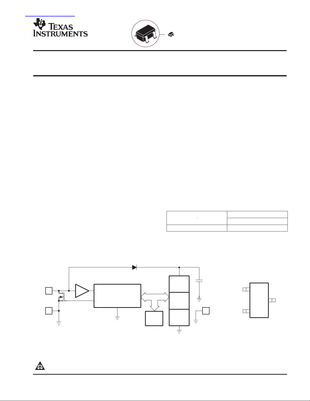
BLOCK DIAGRAM
DBZR P ACKAGE
ID ROM
SDQ 1
2VSS 3 VSS
semiconductor products and disclaimers thereto appears at the end of this data sheet.
!"# $ %&'# "$ (&)%"# *"#'+ *&%#$
%! # $('%%"#$ (' #,' #'!$ '-"$ $#&!'#$ $#"*"* .""#/+
*&%# (%'$$0 *'$ # '%'$$")/ %)&*' #'$#0 ")) (""!'#'$+
SDQ Communications
Controller and 8-Bit CRC
Generation Circuit
Internal
Bus
RAM
Buffer
(8 bytes)
(64 bits)
EPROM
MEMORY
(1024 bits)
EPROM
STATUS
(64 bits)
UDG−02054
Copyright 2003, Texas Instruments Incorporated
(TOP VIEW)
SDQ
VSS
1
VSS
3
2
Page 2

VOLLow-level output voltage
V
t
Recovery time
(1)
s
SLUS526B − OCTOBER 2002 − REVISED OCTOBER 2003
These devices have limited built-in ESD protection. The leads should be shorted together or the device placed in conductive foam during
storage or handling to prevent electrostatic damage to the MOS gates.
www.ti.com
ABSOLUTE MAXIMUM RATINGS
over operating free-air temperature range unless otherwise noted
DC voltage applied to data, V
Low-level output current, I
ESD human body model Data to V
Operating free-air temperature range, T
Communication free-air temperature range, T
Storage temperature range, T
Lead temperature (soldering, 10 s) 260°C
(1)
Stresses beyond those listed under “absolute maximum ratings may cause permanent damage to the device. These are stress ratings only , a nd
functional operation of the device at these or any other conditions beyond those indicated under “recommended operating conditions is not implied.
Exposure to absolute-maximum-rated conditions for extended periods may affect device reliability.
PU
OL
A
A(Comm)
stg
(1)
UNIT
−0.3 V to 7 V
40 mA
SS, VSS
Communication is specified by design −40°C to 85°C
to data 15 kV
−20°C to 70°C
−55°C to 125°C
DC ELECTRICAL CHARACTERISTICS
TA = −20°C to 70°C; V
PARAMETER TEST CONDITION MIN TYP MAX UNIT
I
DATA
V
OH
I
OL
V
IL
V
IH
V
PP
Supply current VPU = 5.5 V 20 µA
High-level output voltage Logic 1 V
Low-level output current (sink) VOL = 0.4 V , SDQ pin 4 mA
Low-level input voltage Logic 0 0.8 V
High-level input voltage Logic 1 2.2 V
Programming voltage 11.5 12 V
= 2.65 VDC to 5.5 VDC, all voltages relative to VSS
PU(min)
Logic 0, VPU = 5.5 V , IOL = 4 mA, SDQ pin 0.4
Logic 0, VPU = 2.65 V , IOL = 2 mA 0.4
PU
5.5
AC ELECTRICAL CHARACTERISTICS
TA = −20°C to 70°C; V
t
c
t
WSTRB
t
WDSU
t
WDH
rec
t
RSTRB
t
ODD
t
ODHO
t
RST
t
PPD
t
PP
t
EPROG
t
PSU
t
PREC
t
PRE
t
PFE
t
RSTREC
(1)
5-kΩ series resistor between SDQ pin and VPU. (See Figure 1)
(2)
t
WDH
Bit cycle time
Write start cycle
Write data setup
Write data hold
Read start cycle
Output data delay
Output data hold
Reset time
Presence pulse delay
Presence pulse
EPROM programming time 2500 µs
Program setup time 5 µs
Program recovery time 5 µs
Program rising-edge time 5 µs
Program falling-edge time 5 µs
must be less than tc to account for recovery.
= 2.65 VDC to 5.5 VDC, all voltages relative to VSS
PU(min)
PARAMETER TEST CONDITION MIN TYP MAX UNIT
(1)
(1)
(1)
(1) (2)
(1)
(1)
(1)
(1)
(1)
(1)
60 120 µs
t
WSTRB
60 t
For memory command only 5
t
RSTRB
17 60 µs
480 µs
15 60 µs
60 240 µs
480 µs
1 15 µs
15 µs
µs
c
1
1 13 µs
µ
13 µs
2
Page 3

www.ti.com
I/O
DESCRIPTION
SLUS526B − OCTOBER 2002 − REVISED OCTOBER 2003
Terminal Functions
TERMINAL
NAME NO.
SDQ 1 I Data
VSS 2, 3 − Ground
FUNCTIONAL DESCRIPTION
General Operation
The block diagram on page 1 shows the relationships among the major control and memory sections of the
bq2022. The bq2022 has three main data components: a 64-bit factory programmed ROM, including 8-bit family
code, 48-bit identification number and 8-bit CRC value, 1024-bit EPROM, and EPROM STATUS bytes. Power
for read and write operations is derived from the DA TA pin. An internal capacitor stores energy while the signal
line is high and releases energy during the low times of the DA TA pin, until the pin returns high to replenish the
charge on the capacitor. A special manufacturer’s PROGRAM PROFILE BYTE can be read to determine the
programming profile required to program the part.
1024-Bits EPROM
Table 1 is a memory map of the 1024-bit EPROM section of the bq2022, configured as four pages of 32 bytes
each. The 8-byte RAM buffer are additional registers used when programming the memory. Data are first written
to the RAM buffer and then verified by reading an 8-bit CRC from the bq2022 that confirms proper receipt of
the data. If the buffer contents are correct, a programming command is issued and an 8-byte segment of data
is written into the selected address in memory. This process ensures data integrity when programming the
memory. The details for reading and programming the 1024-bit EPROM portion of the bq2022 are in the
Memory Function Commands section of this data sheet.
Table 1. 1024-Bit EPROM Data Memory Map
ADDRESS
(HEX)
0060−007F Page 3
0040−005F Page 2
0020−003F Page 1
0000−001F Page 0
PAGE
EPROM STATUS Memory
In addition to the programmable 1024-bits of memory, are 64 bits of status information contained in the EPROM
STATUS memory. The STATUS memory is accessible with separate commands. The STA TUS bits are EPROM
and are read or programmed to indicate various conditions to the software interrogating the bq2022. The first
byte of the STA TUS memory contains the write protect page bits, that inhibit programming of the corresponding
page in the 1024-bit main memory area if the appropriate write-protection bit is programmed. Once a bit has
been programmed in the write protect page byte, the entire 32-byte page that corresponds to that bit can no
longer be altered but may still be read. The write protect bits may be cleared by using the WRITE STATUS
command.
The next four bytes of the EPROM STATUS memory contain the page address redirection bytes. Bits in the
EPROM status bytes can indicate to the host what page is substituted for the page by the appropriate redirection
byte. The hardware of the bq2022 makes no decisions based on the contents of the page address redirection
bytes. This feature allows the user’s software to make a data patch to the EPROM by indicating that a particular
page or pages should be replaced with those indicated in the page address redirection bytes. The ones
complement of the new page address is written into the page address redirection byte that corresponds to the
original (replaced) page. If a page address redirection byte has an FFh value, the data in the main memory that
corresponds to that page are valid. If a page address redirection byte has some other hex value, the data in
the page corresponding to that redirection byte are invalid, and the valid data can now be found at the ones
3
Page 4
SLUS526B − OCTOBER 2002 − REVISED OCTOBER 2003
complement of the page address indicated by the hex value stored in the associated page address redirection
byte. A value of FDh in the redirection byte for page 1, for example, indicates that the updated data are now
in page 2. The details for reading and programming the EPROM status memory portion of the bq2022 are given
in the Memory Function Commands section.
Table 2. EPROM Status Bytes
ADDRESS
(HEX)
Write protection bits
BIT0 − write protect page 0
00h
01h Redirection byte for page 0
02h Redirection byte for page 1
03h Redirection byte for page 2
04h Redirection byte for page 3
05h Reserved
06h Reserved
07h Factory programmed 00h
BIT1 − write protect page 1
BIT2 − write protect page 2
BIT3 − write protect page 3
BIT4 to 7 − bitmap of used pages
PAGE
www.ti.com
Error Checking
To validate the data transmitted from the bq2022, the host generates a CRC value from the data as they are
received. This generated value is compared to the CRC value transmitted by the bq2022. If the two CRC values
match, the transmission is error-free. The equivalent polynomial function of this CRC is X8 + X5 + X4 + 1. Details
are found in the CRC Generation Section of this data sheet.
Customizing the bq2022
The 64-bit ID identifies each bq2022. The 48-bit serial number is unique and programmed by Texas
Instruments. The default 8-bit family code is 09h; however, a different value can be reserved on an individual
customer basis. Contact your Texas Instruments sales representative for more information.
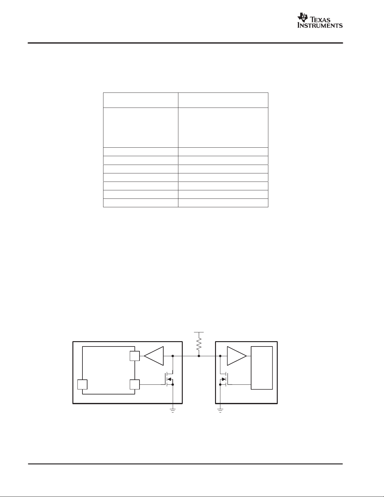
Bus Termination
Because the drive output of the bq2022 is an open-drain N-channel MOSFET, the host must provide a source
current or a 5-kΩ external pullup, as shown in the typical application circuit in Figure 1.
V
PU
1
SDQ
Communications
Controller
3 VSS VSS
2
CPU
HOSTbq2022
UDG−02055
Figure 1. Typical Applications Circuit
4
Page 5
www.ti.com
SLUS526B − OCTOBER 2002 − REVISED OCTOBER 2003
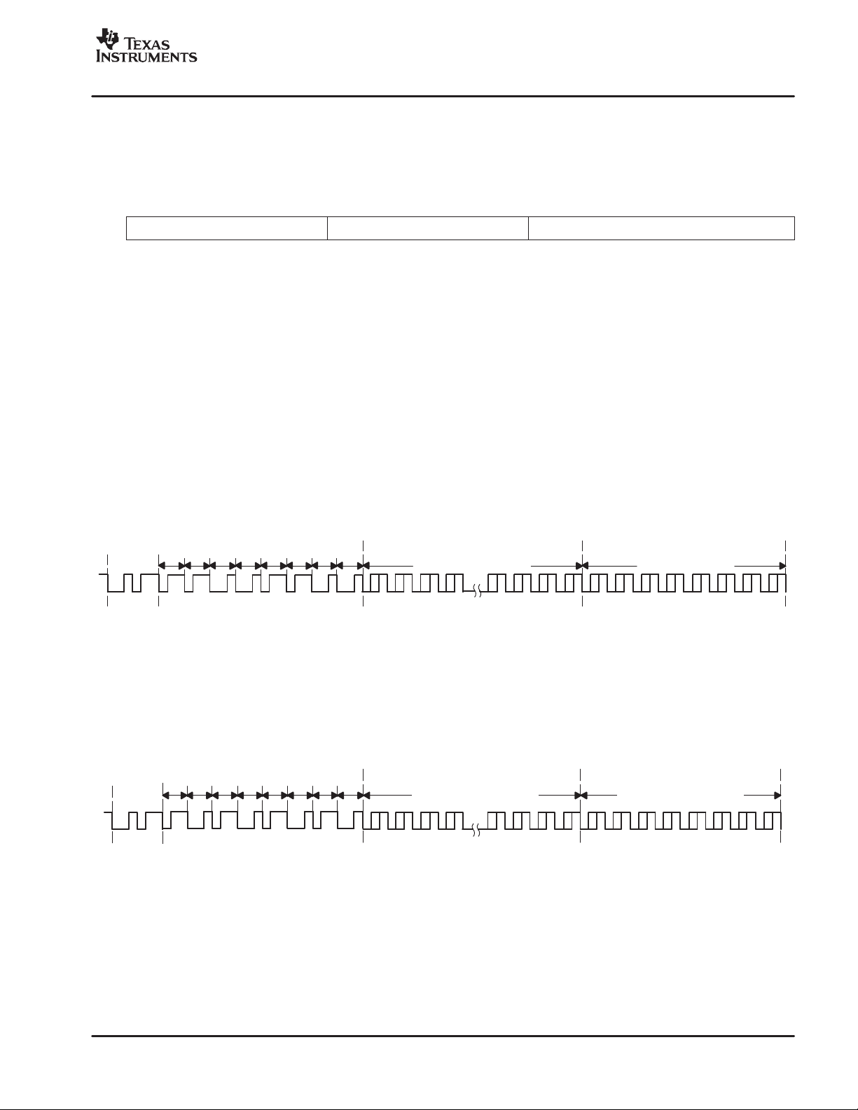
Serial Communication
A host reads, programs, or checks the status of the bq2022 through the hierarchical command structure of the
SDQ interface. Figure 2 shows that the host must first issue a ROM command before the EPROM memory or
status can be read or modified. The ROM command either selects a specific device when multiple devices are
on the SDQ bus, or skips the selection process in single SDQ device applications.
Initialization ROM Command Sequence Memory/Status Command Sequence
Figure 2. General Command Sequence
Initialization
Initialization consists of two pulses, the RESET and the PRESENCE pulses. The host generates the RESET
pulse, while the bq2022 responds with the PRESENCE pulse. The host resets the bq2022 by driving the DATA
bus low for at least 480 µs. For more details, see the RESET section under SDQ Signaling.
ROM Commands
READ ROM
The READ ROM command sequence is the fastest sequence that allows the host to read the 8-bit family code
and 48-bit identification number. It is used if only one SDQ slave device is attached to the bus. The READ ROM
sequence starts with the host generating the RESET pulse of at least 480 µs. The bq2022 responds with a
PRESENCE pulse. Next, the host continues by issuing the READ ROM command, 33h, and then reads the
ROM and CRC byte using the READ signaling (see the READ and WRITE signals section) during the data
frame.
Reset
and
Presence
Signals
Read ROM (33h)
1100011
0
Family Code and Identification
Number (7 BYTES)
CRC (1 BYTE)
Figure 3. READ ROM Sequence
MATCH ROM
The MATCH ROM command, 55h, is used by the host to select a specific SDQ device when the family code
and identification number is known. The host issues the MATCH ROM command followed by the family code,
ROM number and the CRC byte. Only the device that matches the 64-bit ROM sequence is selected and
available to perform subsequent Memory/Status Function commands.
Reset
and
Presence
Signals
Match ROM (55h)
1100011
0
Family Code and Identification
Number (7 BYTES)
CRC (1 BYTE)
Figure 4. MATCH ROM Sequence
SEARCH ROM
The SEARCH ROM command, F0h, is used to obtain the 8-bit family code and the 48-bit identification number
and 8-bit CRC of any SDQ device when it is unknown. All devices on the bus are read under the SEARCH ROM
command with the use of a collision-detect and device-decode method. Figure 5 shows the SEARCH ROM
sequence started by the host, generating the RESET pulse of at least 480 µs. The bq2022 responds with a
PRESENCE pulse. The host then issues the command in the command frame by writing an F0h. During the
DATA READ of the SEARCH ROM sequence, each bit is transmitted three times. The bq2022 transmits the
bit followed by the complement of the bit. The host in turn retransmits the bit just read. Collision detection if
5
Page 6
SLUS526B − OCTOBER 2002 − REVISED OCTOBER 2003
performed by comparing the bit and bit complement time-slots. If they are both zero, this indicates that a collision
has occurred, indicating multiple devices on the bus. The device decode is achieved in the third transmission
of the bit from the host back to the bq2022. If the bit transmitted by the host does not match the bit transmitted
by the bq2022, then the device with mismatch stops transmitting. Devices that did match, continue transmitting.
This process is continued until all bits of a single device are read. The SEARCH ROM command is reissued
and the process is repeated to read additional devices.
NOTE: If the number of devices on the bus is unknown, the SEARCH ROM command should
be used.
Reset
and
Presence
Signals
B = bit(n): nth bit transmitted by bq2022
C = bit(n): complement of nth bit transmitted by bq2022
H = bit(n): nth bit transmitted by host
00001111
Search ROM (F0h)
BIT0
Figure 5. SEARCH ROM Sequence
SKIP ROM
This SKIP ROM command, CCh, allows the host to access the memory/status functions without issuing the
64-bit ROM code sequence. The SKIP ROM command is directly followed by a memory/status functions
command. Because this command can cause bus collisions when multiple SDQ devices are on the same bus,
this command should be issued in single device applications.
Reset
and
Presence
Signals
1000110
Skip ROM (CCh)
Data Read
BITn BIT63
1
www.ti.com
Figure 6. SKIP ROM Sequence
Memory/Status Function Commands
Six memory/status function commands allow read and modification of the 1024-bit EPROM data memory or
the 64-bit EPROM status memory. There are two types of READ MEMORY command, plus the WRITE
MEMORY, READ STATUS and WRITE STATUS commands. Additionally, the part responds to a PROGRAM
PROFILE byte command. The bq2022 responds to memory/status function commands only after a part is
selected by a ROM command.
READ DATA MEMORY Commands
Two READ MEMORY commands are available on the bq2022. Both commands are used to read data from
the 1024-bit EPROM data field. They are the READ MEMORY/Page CRC and the READ MEMORY/Field CRC
commands. The READ MEMORY/Page CRC generates CRC at the end any 32 byte page boundary while the
READ MEMORY/Field CRC generates CRC when the end of the 1024-bit data memory is reached.
READ MEMORY/Page CRC
To read memory and generate the CRC at the 32-byte page boundaries of the bq2022, the ROM command is
followed by the READ MEMORY/Generate CRC command, C3h, followed by the address low byte and then
the address high byte.
6
Page 7

www.ti.com
SLUS526B − OCTOBER 2002 − REVISED OCTOBER 2003
An 8-bit CRC of the command byte and address bytes is computed by the bq2022 and read back by the host
to confirm that the correct command word and starting address were received. If the CRC read by the host is
incorrect, a reset pulse must be issued and the entire sequence must be repeated. If the CRC received by the
host is correct, the host issues read time slots and receives data from the bq2022 starting at the initial address
and continuing until the end of a 32-byte page is reached. At that point the host sends eight additional read time
slots and receive an 8-bit CRC that is the result of shifting into the CRC generator all of the data bytes from
the initial starting byte to the last byte of the current page. Once the 8-bit CRC has been received, data is again
read from the 1024-bit EPROM data field starting at the next page. This sequence continues until the final page
and its accompanying CRC are read by the host. Thus each page of data can be considered to be 33 bytes
long, the 32 bytes of user-programmed EPROM data and an 8-bit CRC that gets generated automatically at
the end of each page.
Initialization and
ROM Command
Sequence
NOTE:Individual bytes of address and data are transmitted LSB first.
READ
MEMORY/Generate
CRC Command
C3h
Address Low Byte
A0 A7
Address High Byte
A8 A15
EPROM Memory and CRC
Byte Generated at 32-Byte
Page Boundaries
Figure 7. READ MEMORY/Page CRC
READ MEMORY/Field CRC
To read memory without CRC generation on 32 byte page boundaries, the ROM command is followed by the
READ MEMORY command, F0h, followed by the address low byte and then the address high byte.
NOTE: As shown in Figure 8, individual bytes of address and data are transmitted LSB first.
An 8-bit CRC of the command byte and address bytes is computed by the bq2022 and read back by the host
to confirm that the correct command word and starting address were received. If the CRC read by the host is
incorrect, a reset pulse must be issued and the entire sequence must be repeated. If the CRC received by the
host is correct, the host issues read time slots and receives data from the bq2022 starting at the initial address
and continuing until the end of the 1024-bit data field is reached or until a reset pulse is issued. If reading occurs
through the end of memory space, the host may issue eight additional read time slots and the bq2022 responds
with a 8-bit CRC of all data bytes read from the initial starting byte through the last byte of memory. After the
CRC is received by the host, any subsequent read time slots appear as logical 1s until a reset pulse is issued.
Any reads ended by a reset pulse prior to reaching the end of memory does not have the 8-bit CRC available.
Initialization and
ROM Command
Sequence
READ
MEMORY
Command
F0h
Address Low
Byte
A0 A7
Address High
Byte
A8 A15
Read and
Verify CRC
Read EEPROM
Memory Until End
of EPROM Memory
Figure 8. READ MEMORY/Field CRC
WRITE MEMORY
The WRITE MEMORY command is used to program the 1024-bit EPROM memory field. The 1024-bit memory
field is programmed in 8-byte segments. Data is first written into an 8-byte RAM buffer one byte at a time. The
contents of the RAM buf fer is then ANDed with the contents of the EPROM memory field when the programming
command is issued.
Figure 9 illustrates the sequence of events for programming the EPROM memory field. After issuing a ROM
command, the host issues the WRITE MEMORY command, 0Fh, followed by the low byte and then the high
byte of the starting address. The bq2022 calculates and transmits an 8-bit CRC based on the WRITE command
and address.
Read and
Verify CRC
7
Page 8

SLUS526B − OCTOBER 2002 − REVISED OCTOBER 2003
If at any time during the WRITE MEMORY process, the CRC read by the host is incorrect, a reset pulse must
be issued, and the entire sequence must be repeated.
After the bq2022 transmits the CRC, the host then transmits 8 bytes of data to the bq2022. Another 8-bit CRC
is calculated and transmitted based on the 8 bytes of data. If this CRC agrees with the CRC calculated by the
host, the host transmits the program command 5Ah and then applies the programming voltage for at least
2500 µs or t
EPROG
EPROM offset by the starting address.
The starting address can be any integer multiple of eight between 0000 and 007F (hex) such as 0000, 0008,
and 0010 (hex).
The WRITE DATA MEMORY command sequence can be terminated at any point by issuing a reset pulse
except during the program pulse period t
NOTE: The bq2022 responds with the data from the selected EPROM address sent least
significant-bit first. This response should be checked to verify the programmed byte. If the
programmed byte is incorrect, then the host must reset the part and begin the write sequence again.
For both of these cases, the decision to continue programming is made entirely by the host, since the bq2022
is not able to determine if the 8-bit CRC calculated by the host agrees with the 8-bit CRC calculated by the
bq2022.
Prior to programming, bits in the 1024-bit EPROM data field appear as logical 1s.
. The contents of the RAM buffer is then logically ANDed with the contents of the 8-byte
.
PROG
www.ti.com
8
Page 9

www.ti.com
SLUS526B − OCTOBER 2002 − REVISED OCTOBER 2003
Selected
State
Write Memory
Command?
(0Fh)
Bus Master TransmitsLow Byte Address
(LSB First) AD0 to AD7
Bus Master Transmits High Byte Address
(LSB First) AD8 to AD15
bq2022
Loads Address Into Address Counter
bq2022 Transmits CRC of Write Command
and Address, and then Clears CRC Register
bq2022 Receives 8 Bytes of Data and
Stores in RAM Buffer
bq2022 Transmits
CRC of Previous Received 8 Bytes of Data
N
Y
Selected
State
Code 5Ah
Received
Contents of RAM buffer AND’ed with contents of
data memory offset by
address counter and stored in data
memory offset by address counter.
programming time required to be at
least t
when VPP Vdc on data pin
EPROG
Transmits 1 Bytes of Data Memory
bq2022
at Address Counter
YN
NOTE: Individual bytes of address and data are transmitted LSB first.
Figure 9. WRITE MEMORY Command Flow
Voltage on Data
Pin = VPP
Y
8th Byte
Transmitted
Y
bq2022 Waits for Reset
(No Further Response)
N
bq2022
Increments Address
Counter and Transmits 1
Byte of Data Memory
Indexed by Address Counter
N
UDG−02061
9
Page 10

SLUS526B − OCTOBER 2002 − REVISED OCTOBER 2003
READ STATUS
The READ STATUS command is used to read data from the EPROM status data field. After issuing a ROM
command, the host issues the READ STATUS command, AAh, followed by the address low byte and then the
address high byte.
NOTE: An 8-bit CRC of the command byte and address bytes is computed by the bq2022 and read
back by the host to confirm that the correct command word and starting address were received.
If the CRC read by the host is incorrect, a reset pulse must be issued and the entire sequence must be repeated.
If the CRC received by the host is correct, the host issues read time slots and receives data from the bq2022
starting at the supplied address and continuing until the end of the EPROM Status data field is reached. At that
point the host receives an 8-bit CRC that is the result of shifting into the CRC generator all of the data bytes
from the initial starting byte through the final factory-programmed byte that contains the 00h value.
This feature is provided since the EPROM status information may change over time making it impossible to
program the data once and include an accompanying CRC that is always valid. Therefore, the READ status
command supplies a 8-bit CRC that is based on (and always is consistent with) the current data stored in the
EPROM status data field.
After the 8-bit CRC is read, the host receives logical 1s from the bq2022 until a reset pulse is issued. The READ
STATUS command sequence can be ended at any point by issuing a reset pulse.
www.ti.com
Initialization and
ROM Command
Sequence
READ STATUS
Command
AAh
Address Low
Byte
A0 A7
Address High
Byte
A8 A15
Read and Verify
CRC
Read
STATUS Memory
Until End of
STATUS Memory
Read and Verify
Figure 10. READ STATUS Command
WRITE STATUS
The Write Status command is used to program the EPROM Status data field after the bq2022 has been selected
by a ROM Command
The flow chart in Figure 11 illustrates that the host issues the Write Status command, 55h, followed by the
address low byte and then the address high byte the followed by the byte of data to be programmed.
NOTE: Individual bytes of address and data are transmitted LSB first. An 8-bit CRC of the command
byte, address bytes, and data byte is computed by the bq2022 and read back by the host to confirm
that the correct command word, starting address, and data byte were received.
If the CRC read by the host is incorrect, a reset pulse must be issued and the entire sequence must be repeated.
If the CRC received by the host is correct, the program command (5Ah) is issued. After the program command
is issued then the programming voltage, VPP is applied to the DA T A pin for period t
. Prior to programming,
PROG
the first seven bytes of the EPROM STATUS data field appear as logical 1s. For each bit in the data byte
provided by the host that is set to a logical 0, the corresponding bit in the selected byte of the EPROM STATUS
data field is programmed to a logical 0 after the programming pulse has been applied at the byte location. The
eighth byte of the EPROM STATUS byte data field is factory-programmed to contain 00h.
CRC
10
Page 11

www.ti.com
SLUS526B − OCTOBER 2002 − REVISED OCTOBER 2003
Selected
State
Write Status
Command?
(55h)
bq2022 Receives Low Address Byte
(LSB First) AD0 to AD7
bq2022 Receives High Address Byte
(LSB First) AD8 to AD15
bq2022 Loads Address Into Address Counter
bq2022 Receives 1 Bytes of Data
and Stores in RAM Buffer
bq2022 Transmits CRC of Write Status
Command, Address, and Data
N
Y
Selected
State
bq2022
Calculates and Transmits
CRC of Loaded Address and
Shifted Data
bq2022
Receives Data Byte
bq2022
Increments Address
Counter and Loads
New Address into CRC
Register
Figure 11. WRITE STATUS Command Flow
Code 5Ah
Received
Contents of RAM buffer AND’ed with contents of
data memory as pointed to by address counter.
Programming time required to be at least
t
when VPP is applied to the data pin
EPROG
bq2022
Transmits Data Byte of
Status Memory Pointed
to by Address Counter
End of Status
Memory?
bq2022 Waits for Reset
YN
N
Y
V
DATA
= VPP?
Y
N
UDG−02064
11
Page 12

ROM Commands
ROM Commands
Available in Command Level I
Memory Function Commands
Memory Function Commands
Available in Command Level II
SLUS526B − OCTOBER 2002 − REVISED OCTOBER 2003
After the programming pulse is applied and the data line returns to VPU, the host issues eight read time slots
to verify that the appropriate bits have been programmed. The bq2022 responds with the data from the selected
EPROM STATUS address sent least significant bit first. This response should be checked to verify the
programmed byte. If the programmed byte is incorrect, then the host must reset the device and begin the write
sequence again. If the bq2022 EPROM data byte programming was successful, the bq2022 automatically
increments its address counter to select the next byte in the ST ATUS MEMORY data field. The least significant
byte of the new two-byte address is also loaded into the 8-bit CRC generator as a starting value. The host issues
the next byte of data using eight write time slots.
As the bq2022 receives this byte of data into the RAM buffer, it also shifts the data into the CRC generator that
has been preloaded with the LSB of the current address and the result is an 8-bit CRC of the new data byte
and the LSB of the new address. After supplying the data byte, the host reads this 8-bit CRC from the bq2022
with eight read time slots to confirm that the address incremented properly and the data byte was received
correctly. If the CRC is incorrect, a Reset Pulse must be issued and the W rite Status command sequence must
be restarted. If the CRC is correct, the host issues a programming pulse and the selected byte in memory is
programmed.
NOTE:The initial write of the WRITE STATUS command, generates an 8-bit CRC value that is the
result of shifting the command byte into the CRC generator, followed by the two-address bytes, and
finally the data byte. Subsequent writes within this WRITE STATUS command due to the bq2022
automatically incrementing its address counter generates an 8-bit CRC that is the result of loading
(not shifting) the LSB of the new (incremented) address into the CRC generator and then shifting
in the new data byte.
www.ti.com
For both of these cases, the decision to continue programming the is made entirely by the host, since the
bq2022 is not able to determine if the 8-bit CRC calculated by the host agrees with the 8-bit CRC calculated
by the bq2022. If an incorrect CRC is ignored and a program pulse is applied by the host, incorrect programming
could occur within the bq2022. Also note that the bq2022 always increments its internal address counter after
the receipt of the eight read time slots used to confirm the programming of the selected EPROM byte. The
decision to continue is again made entirely by the host, therefore if the EPROM data byte does not match the
supplied data byte but the master continues with the WRITE STATUS command, incorrect programming could
occur within the bq2022. The WRITE STATUS command sequence can be ended at any point by issuing a reset
pulse.
Table 3. Command Code Summary
COMMAND
(HEX)
33h Read Serialization ROM and CRC
55h Match Serialization ROM
F0h Search Serialization ROM
CCh Skip Serialization ROM
F0h Read Memory
AAh Read EPROM Status
C3h Read/Generate CRC
0Fh Program Memory
99h Programming Profile
55h Write EPROM Status
5Ah Program Control
DESCRIPTION CATEGORY
Available in Command Level I
Available in Command Level II
Program Command Available Only in WRITE
MEMORY and WRITE STATUS Modes
PROGRAM PROFILE BYTE
The PROGRAM PROFILE byte is read to determine the WRITE MEMORY programming sequence required
by a specific manufacturer. After issuing a ROM command, the host issues the PROGRAM PROFILE BYTE
command, 99h. Figure 12 shows the the bq2022 responds with 55h. This informs the host that the WRITE
MEMORY programming sequence is the one described in the WRITE MEMORY command section of this data
sheet.
12
Page 13

www.ti.com
SLUS526B − OCTOBER 2002 − REVISED OCTOBER 2003
From ROM
Command
Program
Profile Command?
99h
Y
bq2022 Transmits
55h
Master Issues Reset
N
Other
Command
Codes
bq2022 is in
Reset State
Figure 12. PROGRAM PROFILE Command Flow
SDQ Signaling
All SDQt signaling begins with initializing the device, followed by the host driving the bus low to write a 1 or
0, or to begin the start frame for a bit read. Figure 13 shows the initialization timing, while Figure 14 and
Figure 15 show that the host initiates each bit by driving the DATA bus low for the start period, t
WSTRB
After the bit is initiated, either the host continues controlling the bus during a WRITE, or the bq2022 responds
during a READ.
RESET AND PRESENCE PULSE
If the DATA bus is driven low for more than 120 µs, the bq2022 may be reset. Figure 13 shows that if the DATA
bus is driven low for more than 480 µs, the bq2022 resets and indicates that it is ready by responding with a
PRESENCE PULSE.
UDG−02067
/ t
RSTRB
.
RESET
V
PU
V
IH
V
IL
(Sent by Host)
t
RST
t
PPD
Presence Pulse
(Sent by bq2022)
t
PP
t
RSTREC
Figure 13. Reset Timing Diagram
WRITE
The WRITE bit timing diagram in Figure 14 shows that the host initiates the transmission by issuing the t
portion of the bit and then either driving the DATA bus low for a WRITE 0, or releasing the DATA bus for a
WRITE 1.
V
PU
V
IH
V
IL
t
WSTRB
t
WDSU
t
WDH
Write ”1”
Write ”0”
t
rec
Figure 14. Write Bit Timing Diagram
UDG−02067
WSTRB
13
Page 14

SLUS526B − OCTOBER 2002 − REVISED OCTOBER 2003
READ
The READ bit timing diagram in Figure 15 shows the host initiates the transmission of the bit by issuing the
t
RSTRB
or releasing the DATA bus to transmit a READ 1.
portion of the bit. The bq2022 then responds by either driving the DA TA bus low to transmit a READ 0
www.ti.com
V
PU
V
IH
V
IL
t
RSTRB
t
ODD
t
ODHO
Read ”1”
Read ”0”
t
REC
Figure 15. Read Bit Timing Diagram
IDLE
If the bus is high, the bus is in the IDLE state. Bus transactions can be suspended by leaving the DATA bus
in IDLE. Bus transactions can resume at any time from the IDLE state.
CRC Generation
The bq2022 has an 8-bit CRC stored in the most significant byte of the 64-bit ROM. The bus master can
compute a CRC value from the first 56 bits of the 64-bit ROM and compare it to the value stored within the
bq2022 to determine if the ROM data has been received error-free by the bus master. The equivalent polynomial
function of this CRC is: X8 + X5 + X4 +1.
Under certain conditions, the bq2022 also generates an 8-bit CRC value using the same polynomial function
shown above and provides this value to the bus master to validate the transfer of command, address, and data
bytes from the bus master to the bq2022. The bq2022 computes an 8-bit CRC for the command, address, and
data bytes received for the WRITE MEMORY and the WRITE STATUS commands and then outputs this value
to the bus master to confirm proper transfer. Similarly the bq2022 computes an 8-bit CRC for the command
and address bytes received from the bus master for the READ MEMORY, READ STATUS, and READ DATA/
GENERATE 8-BIT CRC commands to confirm that these bytes have been received correctly. The CRC
generator on the bq2022 is also used to provide verification of error-free data transfer as each page of data from
the 1024-bit EPROM is sent to the bus master during a READ DA TA/GENERATE 8-BIT CRC command, and
for the eight bytes of information in the status memory field.
In each case where a CRC is used for data transfer validation, the bus master must calculate a CRC value using
the polynomial function given above and compare the calculated value to either the 8-bit CRC value stored in
the 64-bit ROM portion of the bq2022 (for ROM reads) or the 8-bit CRC value computed within the bq2022. The
comparison of CRC values and decision to continue with an operation are determined entirely by the bus
master. There is no circuitry on the bq2022 that prevents a command sequence from proceeding if the CRC
stored in or calculated by the bq2022 does not match the value generated by the bus master. Proper use of
the CRC as outlined in the circuit shown in Figure 16 can result in a communication channel with a high level
of integrity.
V
PP
V
PU
V
SS
t
PSU
t
PRE
t
EPROG
t
PFE
t
PREC
Figure 16. Program Pulse Timing Diagram
14
Page 15

www.ti.com
SLUS526B − OCTOBER 2002 − REVISED OCTOBER 2003
CLK
DAT
QRD QRD QRD QRD QRD QRD QRD QRD
+++
Figure 17. 8-Bit CRC Generator Circuit (X8 + X5 + X4 + 1)
UDG−02065
15
Page 16

SLUS526B − OCTOBER 2002 − REVISED OCTOBER 2003
www.ti.com
MECHANICAL DATA
DBZ (R-PDSO-G3) PLASTIC SMALL-OUTLINE
3,04
2,80
2,05
1,78
1,03
0,89
0,51
0,37
0,60
0,45
1,40
1,20
2,64
2,10
1,12
0,89
NOTES: A. All linear dimensions are in millimeters.
B. This drawing is subject to change without notice.
C. Dimensions are inclusive of plating.
D. Dimensions are exclusive of mold flash and metal burr.
0,100
0,013
0,55 REF
0,180
0,085
4203227/A 08/01
16
Page 17

PACKAGE OPTION ADDENDUM
www.ti.com
14-Mar-2005
PACKAGING INFORMATION
Orderable Device Status
(1)
Package
Type
Package
Drawing
Pins Package
Qty
Eco Plan
BQ2022DBZR ACTIVE SOT-23 DBZ 3 3000 Green (RoHS &
no Sb/Br)
BQ2022DBZRG4 ACTIVE SOT-23 DBZ 3 3000 Green (RoHS &
no Sb/Br)
(1)
The marketing status values are defined as follows:
ACTIVE: Product device recommended for new designs.
LIFEBUY: TI has announced that the device will be discontinued, and a lifetime-buy period is in effect.
NRND: Not recommended for new designs. Device is in production to support existing customers, but TI does not recommend using this part in
a new design.
PREVIEW: Device has been announced but is not in production. Samples may or may not be available.
OBSOLETE: TI has discontinued the production of the device.
(2)
Eco Plan - May not be currently available - please check http://www.ti.com/productcontent for the latest availability information and additional
product content details.
None: Not yet available Lead (Pb-Free).
Pb-Free (RoHS): TI's terms "Lead-Free" or "Pb-Free" mean semiconductor products that are compatible with the current RoHS requirements
for all 6 substances, including the requirement that lead not exceed 0.1% by weight in homogeneous materials. Where designed to be soldered
at high temperatures, TI Pb-Free products are suitable for use in specified lead-free processes.
Green (RoHS & no Sb/Br): TI defines "Green" to mean "Pb-Free" and in addition, uses package materials that do not contain halogens,
including bromine (Br) or antimony (Sb) above 0.1% of total product weight.
(3)
MSL, Peak Temp. -- The Moisture Sensitivity Level rating according to the JEDECindustry standard classifications, and peak solder
temperature.
(2)
Lead/Ball Finish MSL Peak Temp
CU NIPDAU Level-1-260C-UNLIM
CU NIPDAU Level-1-260C-UNLIM
(3)
Important Information and Disclaimer:The information provided on this page represents TI's knowledge and belief as of the date that it is
provided. TI bases its knowledge and belief on information provided by third parties, and makes no representation or warranty as to the
accuracy of such information. Efforts are underway to better integrate information from third parties. TI has taken and continues to take
reasonable steps to provide representative and accurate information but may not have conducted destructive testing or chemical analysis on
incoming materials and chemicals. TI and TI suppliers consider certain information to be proprietary, and thus CAS numbers and other limited
information may not be available for release.
In no event shall TI's liability arising out of such information exceed the total purchase price of the TI part(s) at issue in this document sold by TI
to Customer on an annual basis.
Addendum-Page 1
Page 18

MECHANICAL DATA
MPDS108 – AUGUST 2001
DBZ (R-PDSO-G3) PLASTIC SMALL-OUTLINE
3,04
2,80
2,05
1,78
1,03
0,89
0,51
0,37
0,60
0,45
1,40
1,20
2,64
2,10
1,12
0,89
NOTES: A. All linear dimensions are in millimeters.
B. This drawing is subject to change without notice.
C. Dimensions are inclusive of plating.
D. Dimensions are exclusive of mold flash and metal burr.
0,100
0,013
0,55 REF
0,180
0,085
4203227/A 08/01
POST OFFICE BOX 655303 • DALLAS, TEXAS 75265
Page 19

IMPORTANT NOTICE
Texas Instruments Incorporated and its subsidiaries (TI) reserve the right to make corrections, modifications,
enhancements, improvements, and other changes to its products and services at any time and to discontinue
any product or service without notice. Customers should obtain the latest relevant information before placing
orders and should verify that such information is current and complete. All products are sold subject to TI’s terms
and conditions of sale supplied at the time of order acknowledgment.
TI warrants performance of its hardware products to the specifications applicable at the time of sale in
accordance with TI’s standard warranty. Testing and other quality control techniques are used to the extent TI
deems necessary to support this warranty . Except where mandated by government requirements, testing of all
parameters of each product is not necessarily performed.
TI assumes no liability for applications assistance or customer product design. Customers are responsible for
their products and applications using TI components. To minimize the risks associated with customer products
and applications, customers should provide adequate design and operating safeguards.
TI does not warrant or represent that any license, either express or implied, is granted under any TI patent right,
copyright, mask work right, or other TI intellectual property right relating to any combination, machine, or process
in which TI products or services are used. Information published by TI regarding third-party products or services
does not constitute a license from TI to use such products or services or a warranty or endorsement thereof.
Use of such information may require a license from a third party under the patents or other intellectual property
of the third party, or a license from TI under the patents or other intellectual property of TI.
Reproduction of information in TI data books or data sheets is permissible only if reproduction is without
alteration and is accompanied by all associated warranties, conditions, limitations, and notices. Reproduction
of this information with alteration is an unfair and deceptive business practice. TI is not responsible or liable for
such altered documentation.
Resale of TI products or services with statements different from or beyond the parameters stated by TI for that
product or service voids all express and any implied warranties for the associated TI product or service and
is an unfair and deceptive business practice. TI is not responsible or liable for any such statements.
Following are URLs where you can obtain information on other Texas Instruments products and application
solutions:
Products Applications
Amplifiers amplifier.ti.com Audio www.ti.com/audio
Data Converters dataconverter.ti.com Automotive www.ti.com/automotive
DSP dsp.ti.com Broadband www.ti.com/broadband
Interface interface.ti.com Digital Control www.ti.com/digitalcontrol
Logic logic.ti.com Military www.ti.com/military
Power Mgmt power.ti.com Optical Networking www.ti.com/opticalnetwork
Microcontrollers microcontroller.ti.com Security www.ti.com/security
Telephony www.ti.com/telephony
Video & Imaging www.ti.com/video
Wireless www.ti.com/wireless
Mailing Address: Texas Instruments
Post Office Box 655303 Dallas, Texas 75265
Copyright 2005, Texas Instruments Incorporated
 Loading...