

查询BQ2018供应商
bq2018
Power Minder™ IC
Features
Multifunction charge/discharge
➤
counter
Resolves signals less than 12.5µV
➤
Internal offset calibration im
➤
proves accuracy
1024 bits of NVRAM configured as
➤
128x8
Internal temperature sensor for
➤
self-discharge estimation
Single-wire serial interface
➤
➤ Dual operating modes:
Operating: <80µA
-
- Sleep: <10µA
➤ REG output for low-cost mi-
croregulation
➤ Internal timebase eliminates ex-
ternal components
➤ 8-pin TSSOP or SOIC allows bat-
tery pack integration
General Description
The bq2018 is a low-cost charge/dis
charge counter peripheral packaged in
an 8-pin TSSOP or SOIC. It works
with an intelligent host controller, pro
viding state-of-charge information for
rechargeable batteries.
The bq2018 measures the voltage
drop across a low-value series sense
resistor between the negative termi
nal of the battery and the battery
pack ground contact. By using the ac
cumulated counts in the charge,
discharge, and self-discharge registers, an intelligent host controller can
determine battery state-of-charge information. To improve accuracy, an
offset count register is available. The
system host controller is responsible
for the register maintenance by resetting the charge in/out and selfdischarge registers as needed.
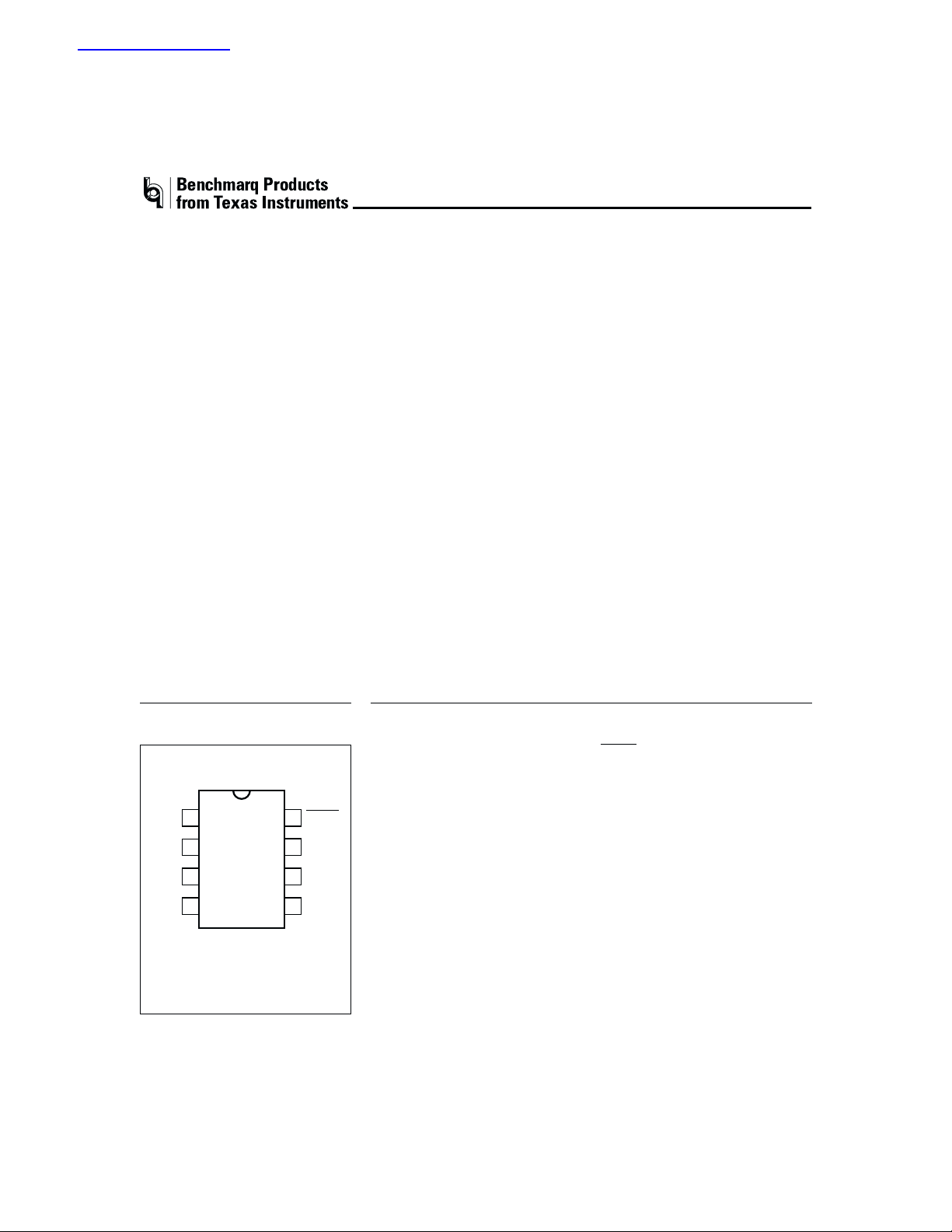
Pin Connections Pin Names
The bq2018 also features 128 bytes
of NVRAM registers. The upper 13
bytes of NVRAM contain the capac
ity monitoring and status informa
tion. The RBI input operates from
an external power storage source
such as a capacitor or a series cell in
the battery pack, providing register
nonvolatility for periods when the
battery is shorted to ground or when
the battery charge state is not suffi
cient to operate the bq2018. During
this mode, the register backup cur
rent is less than 100nA.
-
Packaged in an 8-pin TSSOP or
SOIC, the bq2018 is small enough
to fit in the crevice between two Asize cells or within the width of a
prismatic cell.
-
-
-
-
REG
V
CC
V
SS
HDQ
SLUS003–JUNE 1999 C
1
2
3
4
8-Pin TSSOP or Narrow SOIC
8
7
6
5
PN-201801.eps
WAKE
SR1
SR2
RBI
REG Regulator output
V
CC
V
SS
HDQ Data input/output
Supply voltage input
Ground
1
WAKE Wake-up output
SR1 Current sense input 1
SR2 Current sense input 2
RBI Register backup input

bq2018
Pin Descriptions
REG
V
CC
V
SS
SR1–
SR2
HDQ
RBI
WAKE
Regulator output
REG is the output of the operational trans
conductance amplifier (OTA) that drives an
external pass n-channel JFET to provide an
optional regulated supply. The supply is
regulated at 3.7V nominal.
Supply voltage input
When regulated by the REG output, VCCis
3.7V ±200mV. When the REG output is not
used, the valid operating range is 2.8V to
5.5V.
Ground
Current sense inputs
The bq2018 interprets charge and discharge
activity by monitoring and integrating the
voltage drop (V
The SR1 input connects to the sense resistor
and the negative terminal of the battery.
The SR2 input connects to the sense resistor
and the negative terminal of the pack. V
<V
indicates discharge, and V
SR2
indicates charge. The effective voltage drop,
V
, as seen by the bq2018, is VSR+VOS.
SRO
Valid input range is±200mV.
Data input/output
This bi-directional input/output communicates the register information to the host
system. HDQ is open drain and requires a
pullup/down resistor in the battery pack to
disable/enable sleep mode if the pack is re
moved from the system.
Register backup input
This input maintains the internal register
states during periods when V
minimum operating voltage.
Wake-up output
When asserted, this output is used to indi
cate that the charge or discharge activity is
above a programmed minimal level.
) across pins SR1 and SR2.
SR
SR1>VSR2
is below the
CC
Functional Description
General Operation
A host can use the bq2018 internal counters and timers
to measure battery state-of-charge, estimate selfdischarge, and calculate the average charge and dis
charge current into and out of a rechargeable battery.
The bq2018 needs an external host system to perform all
register maintenance. Using information from the
bq2018, the system host can determine the battery
state-of-charge, estimate self-discharge, and calculate
the average charge and discharge currents. During pack
storage periods, the use of an internal temperature sen
sor doubles the self-discharge count rate every 10° above
25°C.
To reduce cost, power to the bq2018 may be derived using
a low-cost external FET in conjunction with the REG pin.
The bq2018 operating current is less than 80µA. When
the HDQ line remains low for greater than ten seconds
and V
SRO(VSR+VOS
tween SR1 and SR2 and VOSis the offset voltage) is below
the programmed minimal level (WAKE is in High Z), the
bq2018 enters a sleep mode of <10µA where all operations are suspended. HDQ transitioning high reinitiates
the bq2018.
SR1
A register is available to store the calculated offset, allowing current calibration. The offset cancellation register is
written by the bq2018 during pack assembly and is available to the host system to adjust the current measurements. By adding or subtracting the offset value stored
in the OFR, the true charge and discharge counts can be
calculated to a high degree of certainty.
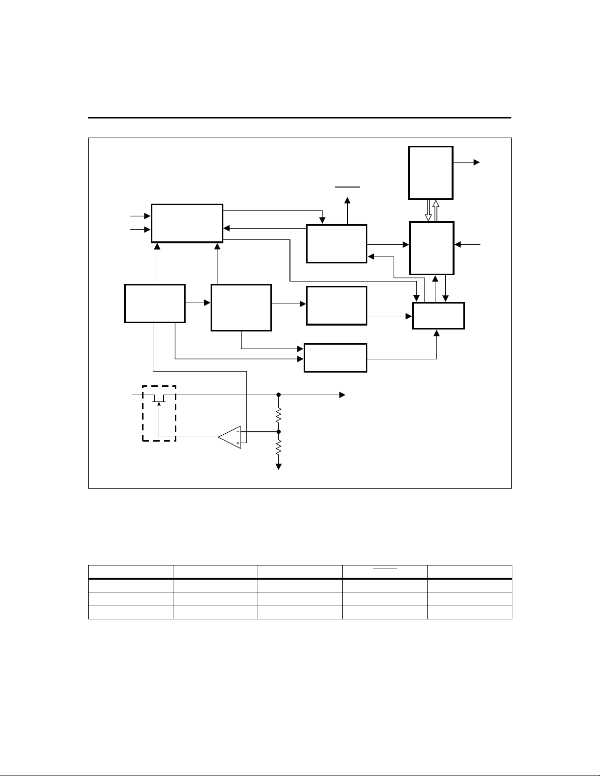
Figure 1 shows a block diagram of the bq2018, and Table
1 outlines the bq2018 operational states.
-
REG Output
The bq2018 can operate directly from three or four
nickel-chemistry cells or a single Li-Ion cell as long as
VCCis limited to 2.8 to 5.5V. To facilitate the power sup
ply requirements of the bq2018, a REG output is present
to regulate an external low-threshold n-JFET. A micro
power VCCsource for the bq2018 can inexpensively be
built using this FET.
-
where VSRis the voltage drop be-
-
-
-
-
2
bq2018
SR1
SR2
Optional
(External)
Dynamically
Balanced VFC
Bandgap
Voltage
Reference
ds
g
Differential
V
CC
REG
Temperature-
Compensated
Precision
Oscillator
WAKE
Calibration
and Power
Control
Timer
Temperature
Sensor
VDD (Internal)
System
I/O
and
Control
RAM
and
Counters
128 x 8
Counter
Control
HDQ
RBI
V
ref
V
SS
Figure 1. bq2018 Block Diagram
Table 1. Operational States
HDQ Pin DCR/CCR/SCR WOE WAKE Operating State
HDQ High yes |V
HDQ High yes |V
HDQ Low no |V
Note: V
is the voltage difference between SR1 and SR2 plus the offset voltage VOS.
SRO
SRO
SRO
SRO
| > V
| < V
| < V
3
WOE
WOE
WOE
Low Normal
High Z Normal
High Z Sleep
BD201801.eps
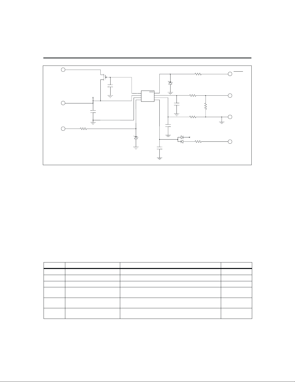
bq2018
BAT+
d
Q1
SST113
s
C5
0.01µF
VCC
1
2
3
45
VCC
C1
0.1µF
R5
HDQ
100
2
D1
BZX84C5V6
Figure 2. Typical Application
RBI Input
The RBI input pin is used with a storage capacitor or external supply to provide back-up potential to the internal
RAM when VCCdrops below 2.4V. The maximum discharge current is 100nA in this mode. The bq2018 outputs VCCon RBI when the supply is above 2.4V, so a diode is required to isolate an external supply.
Charge/Discharge Count Operation
Table 2 shows the main counters and registers of the
bq2018. The bq2018 accumulates charge and discharge
counts into two main count registers, the Discharge
Count Register (DCR) and the Charge Count Register
(CCR). The bq2018 produces charge and discharge
R6
R2
100K
R3
100K
1K
R1
0.05
1W
2
D2
U1
8
WAKE
REG
7
SR1
VCC
6
SR2
VSS
RBI
HDQ
BQ2018
BZX84C5V6
C2
0.1µF
C3
0.1µF
D3
R4
C4
BAV99
0.1µF
1M
2018typAp.eps
counts by sensing the voltage difference across a lowvalue resistor between the negative terminal of the battery pack and the negative terminal of the battery. The
DCR or CCR counts depending on the signal between
SR1 and SR2.
During discharge, the DCR and the Discharge Time
Counter (DTC) are active. If V
cating a discharge, the DCR counts at a rate equivalent to
is less than V
SR1
12.5µV every hour, and the DTC counts at a rate of 1
count/0.8789 seconds (4096 counts per 1 hour). For exam
ple, a -100mV signal produces 8000 DCR counts and 4096
DTC counts each hour. The amount of charge removed
from the battery can easily be calculated.
WAKE
BAT-
PACK-
RBI
SR2
, indi-
-
Table 2. bq2018 Counters
Name Description Range RAM Size
DCR Discharge count register
CCR Charge count register
< V
V
SR1
V
SR1>VSR2
(Max. =-200mV) 12.5µVh increments
SR2
(Max. = +200mV) 12.5µVh increments
SCR Self-discharge count register 1 count/hour @ 25°C 16-bit
DTC Discharge time counter
CTC Charge time counter
MODE/
WOE
MODE/
Wake output enable
1 count/0.8789s default
1 count/225s if STD is set
1 count/0.8789s default
1 count/225s if STC is set
— 8-bit
4
16-bit
16-bit
16-bit
16-bit

bq2018
7f
73
72
User
RAM
00
Figure 3. Address Map
During charge, the CCR and the Charge Time Counter
(CTC) are active. If V
a charge, the CCR counts at a rate equivalent to 12.5µV
every hour, and the CTC counts at a rate of 1
count/0.8789 seconds. For example, a +100mV signal produces 8000 CCR counts and 4096 CTC counts each hour.
The amount of charge added to the battery can easily be
calculated.
The DTC and the CTC are 16-bit registers, and roll over
beyond ffffh. If a rollover occurs, the corresponding bit in
the MODE/WOE register is set, and the counter will subsequently increment at 1/256 of the normal rate (16
counts/hr.).
Whenever the signal between SR1 and SR2 is above the
Wakeup Output Enable (WOE) threshold and the HDQ
pin is high, the bq2018 is in its full operating state. In
this state, the DCR, CCR, DTC, CTC, and SCR are fully
operational, and the WAKE output is low. During this
mode, the internal RAM registers of the bq2018 may be
accessed over the HDQ pin, as described in the section
“Communicating With the 2018.”
If the signal between SR1 and SR2 is below the WOE
threshold (refer to the WAKE section for details) and
HDQ remains low for greater than 10 seconds, the
bq2018 enters a sleep mode where all register counting is
suspended. The bq2018 remains in this mode until HDQ
returns high.
For self-discharge calculation, the self-discharge count
register (SCR) counts at a rate equivalent to 1 count
every hour at a nominal 25°C and doubles approximately
every 10°C up to 60°C. The SCR count rate is halved
every 10 °C below 25°C down to 0°C. The value in SCR is
is greater than V
SR1
, indicating
SR2
7f
Discharge count high byte
7e
Discharge count low byte
7d
Charge count high byte
7c
Charge count low byte
7b
Self-discharge high byte
7a
Self-discharge low byte
79
Discharge time high byte
78
Discharge time low byte
77
Charge time high byte
76
Charge time low byte
75
Mode/wake output enable
74
Temperature/clear
73
Offset register
FG201801.eps
useful in determining an estimation of the battery selfdischarge based on capacity and storage temperature
conditions.
The bq2018 may be programmed to measure the voltage
offset between SR1 and SR2 during pack assembly or at
any time by invoking the Calibration mode. The Offset
Register (OFR) is used to store the bq2018 offset. The 8bit 2’s complement value stored in the OFR is scaled to
the same units as the DCR and CCR, representing the
amount of positive or negative offset in the bq2018. The
maximum offset for the bq2018 is specified as±500µV.
Care should be taken to ensure proper PCB layout. Using OFR, the system host can cancel most of the effects of
bq2018 offset for greater resolution and accuracy.
Figure 3 shows the bq2018 register address map. The
bq2018 uses the upper 13 locations. The remaining
memory can store user-specific information such as
chemistry, serial number, and manufacturing date.
WAKEOutput
This output is used to inform the system that the voltage
difference between SR1 and SR2 is above or below the
Wake Output Enable (WOE) threshold programmed in
the MODE/WOE register. When the voltage difference
between SR1 and SR2 is below V
goes into High Z and remains in this state until the dis
charge or charge current increases above the specified
value. The MODE/WOE resets to 0eh after a power-on
reset. V
tween 1 and 7 (1–7h) according to Table 3.
is set by dividing 3.84mV by a value be
WOE
, the WAKE output
WOE
-
-
5
bq2018
T ab le 3. WOE Thresholds
WOE
(hex) V
3–1
WOE
(mV)
0h n/a
1h 3.840
2h 1.920
3h 1.280
4h 0.960
5h 0.768
6h 0.640
7h* 0.549
* Default value after POR.
Temperature
The bq2018 has an internal temperature sensor which is
used to set the value in the temperature register
(TMP/CLR) and set the self-discharge count rate value.
The register reports the temperature in 8 steps of 10°C
from <0°C to >60°C as Table 4 specifies. The bq2018 temperature sensor has typical accuracy of
2°Cat 25°C.
±
See the TMP/CLR register description for more details.
Clear Register
The host system is responsible for register maintenance.
To facilitate this maintenance, the bq2018 has a Clear
Register (TMP/CLR) designed to reset the specific counter or register pair to zero. The host system clears a register by writing the corresponding register bit to 1. When
the bq2018 completes the reset, the corresponding bit in
the TMP/CLR register is automatically reset to 0, which
saves the host an extra write/read cycle. Clearing the
DTC register clears the STD bit and sets the DTC count
rate to the default value of 1 count per 0.8789s. Clearing
Table 4. Temperature Steps
Temp Value (hex) SDR Count Rate
<0° 0h
0–10° 1h
10–20° 2h
1/8
×
1/4
×
1/2
×
20–30° 3h 1 count/hr.
30–40° 4h
40–50° 5h
50–60° 6h
>60° 7h
2
×
4
×
8
×
16
×
the CTC register clears the STC bit and sets the CTC
count rate to the default value of 1 count per 0.8789s.
Calibration Mode
The system can enable bq2018 VOScalibration by setting
the calibration bit in the MODE/WOE register (Bit 6) to
1. The bq2018 then enters calibration mode when the
HDQ line is low for greater than 10 seconds and when
the signal between SR1 and SR2 is below V
tion: Take care to ensure that no low-level external signal is present between SR1 and SR2 because
this affects the calibration value that the bq2018
calculates.
If HDQ remains low for one hour and |V
the entire time, the measured VOSis latched into the
OFR register, and the calibration bit is reset to zero, indi
cating to the system that the calibration cycle is com
plete. Once calibration is complete, the bq2018 enters a
SR
WOE
|<V
. Cau-
for
WOE
-
-
Written by Host to bq2018
Break
MSB
LSB
0 1 2 3 4 5 6 7
110
LSB
73h = 0 1 1 1 0 0 1 1
Figure 4. Typical Communication with the bq2018
CMDR = 73h
01110
MSB
Received by Host from bq2018
LSB
0
1
Data (OFR) = 65h
1 2 3 4 5 6
010011
MSB LSB
MSB
7
0
65h = 0 1 1 0 0 1 0 1
TD201801.eps
6

Table 5. bq2018 Command and Status Registers
Symbol
CMDR
DCRH
DCRL
CCRH
CCRL
SCRH
SCRL
DTCH
DTCL
CTCH
CTCL
MODE/
WOE
TMP/CLR
OFR
RAM
Notes: 1. MODE/WOE register bit 0 is set to zero at startup and should not be
Register
Name
Command
register
Discharge count
register high
byte
Discharge
count register
low byte
Charge count
register
high byte
Charge count
register
low byte
Self-discharge
count register
high byte
Self-discharge
count register
low byte
Discharge
time count
high byte
Discharge
time count
low byte
Charge
time count
high byte
Charge
time count
low byte
MODE/ wakeup output
enable
Tempera
ture/Clear
register
Offset
register
User
memory
written to 1 for proper bq2018 operation.
2. OFR value is in two’s complement.
Loc.
(hex)
-
72-00
Read/
Write
7(MSB) 6543210(LSB)
- Write W/R
7f Read DCRH7 DCRH6 DCRH5 DCRH4 DCRH3 DCRH2 DCRH1 DCRH0
7e Read DCRL7 DCRL6 DCRL5 DCRL4 DCRL3 DCRL2 DCRL1 DCRL0
7d Read CCRH7 CCRH6 CCRH5 CCRH4 CCRH3 CCRH2 CCRH1 CCRH0
7c Read CCRL7 CCRL6 CCRL5 CCRL4 CCRL3 CCRL2 CCRL1 CCRL0
7b Read SCRH7 SCRH6 SCRH5 SCRH4 SCRH3 SCRH2 SCRH1 SCRH0
7a Read SCRL7 SCRL6 SCRL5 SCRL4 SCRL3 SCRL2 SCRL1 SCRL0
79 Read DTCH7 DTCH6 DTCH5 DTCH4 DTCH3 DTCH2 DTCH1 DTCH0
78 Read DTCL7 DTCL6 DTCL5 DTCL4 DTCL3 DTCL2 DTCL1 DTCL0
77 Read CTCH7 CTCH6 CTCH5 CTCH4 CTCH3 CTCH2 CTCH1 CTCH0
76 Read CTCL7 CTCL6 CTCL5 CTCL4 CTCL3 CTCL2 CTCL1 CTCL0
Read/
75
74
73
OVRDQ CAL STC STD WOE3 WOE2 WOE1 0
write
Read/
write
Read/
write
Read/
write
TMP2 TMP1 TMP0 CTC DTC SCR CCR DCR
OFR7 OFR6 OFR5 OFR4 OFR3 OFR2 OFR1 OFR0
AD6 AD5 AD4 AD3 AD2 AD1 AD0
--------
Control Field
bq2018
7

bq2018
low-power mode until HDQ goes high, indicating an ex
ternal system is ready to access the bq2018. If HDQ
transitions high prior to completion of the VOScalculation
or if |VSR|>V
The bq2018 then postpones the calibration cycle until the
, then the calibration cycle is reset.
WOE
conditions are met. The calibration bit does not reset to
zero until a valid calibration cycle is completed. The re
quirement for HDQ to remain low for the calibration cy
cle can be disabled by setting the OVRDQ bit to 1. In this
case, calibration continues as long as |V
OVRDQ bit is reset to zero at the end of a valid calibra
SR
|<V
WOE
. The
tion cycle.
Communicating with the bq2018
The bq2018 includes a simple single-pin (referenced to
VSS) serial data interface. A host processor uses the in
terface to access various bq2018 registers. Battery activ
ity may be easily monitored by adding a single contact to
the battery pack. Note: The HDQ pin requires an ex
ternal pull-up or pull-down resistor.
The interface uses a command-based protocol, where the
host processor sends a command byte to the bq2018. The
command directs the bq2018 either to store the next
eight bits of data received to a register specified by the
command byte or to output the eight bits of data from a
register specified by the command byte.
The communication protocol is asynchronous return-toone. Command and data bytes consist of a stream of
eight bits that have a maximum transmission rate of 5K
bits/sec. The least-significant bit of a command or data
byte is transmitted first. The protocol is simple enough
that it can be implemented by most host processors using
either polled or interrupt processing. Data input from the
bq2018 may be sampled using the pulse-width capture
timers available on some microcontrollers. A UART may
also be used to communicate through the HDQ pin.
If a communication time-out occurs, e.g., the host waits
longer than t
the first access command, then a BREAK should be sent
by the host. The host may then resend the command. The
bq2018 detects a BREAK when the HDQ pin is driven to
a logic-low state for a time, tBor greater. The HDQ pin
then returns to its normal ready-high logic state for a
time, tBR. The bq2018 is then ready to receive a com
mand from the host processor.
The return-to-one data bit frame consists of three distinct
sections. The first section is used to start the transmis
sion by either the host or the bq2018 taking the HDQ pin
to a logic-low state for a period, t
is the actual data transmission, where the data should be
valid by a period, t
start communication. The data should be held for a peri
od, tDV/tDH, to allow the host or bq2018 to sample the
data bit.
for the bq2018 to respond or if this is
CYCB
. The next section
STRH,B
, after the negative edge used to
DSU,B
The final section is used to stop the transmission by re
turning the HDQ pin to a logic-high state by at least a
period, t
munication. The final logic-high state should be held un
til a period, t
transmission ceased properly. The serial communication
timing specification and illustration sections give the
timings for data and break communication.
-
, after the negative edge used to start com
SSU,B
, to allow time to ensure that the bit
CYCH,B
Communication with the bq2018 always occurs with the
least-significant bit being transmitted first. Figure 4 shows
an example of a communication sequence to read the
bq2018 OFR register.
bq2018 Registers
The bq2018 command and status registers are listed in
Table 5 and described below.
-
Command (CMDR)
-
The write-only command register is accessed when the
bq2018 has received eight contiguous valid command
bits. The command register contains two fields:
n
W/R
n
Command address
The W/R bit of the command register is used to select
whether the received command is for a read or a write
function. The W/R values are
CMDR Bits
76543 21 0
W/R
Where W/R is
The lower seven-bit field of CMDR contains the address
portion of the register to be accessed.
-
Discharge Count Registers(DCRH/DCRL)
The DCRH high-byte register (address = 7fh) and the
DCRL low-byte register (address = 7eh) contain the count
- -- - - - -
0 The bq2018 outputs the requested register
contents specified by the address portion of
the CMDR
1 The following eight bits should be written
to the register specified by the address por
tion of the CMDR
CMDR Bits
76543 21 0
- AD6 AD5 AD4 AD3 AD2 AD1 AD0
-
-
-
-
8

bq2018
of the discharge, and are incremented whenever V
V
. These registers continue to count beyond ffffh, so
SR2
proper register maintenance should be done by the host
SR1
system. The TMP/CLR register is used to force the reset
of both the DCRH and DCRL to zero.
Charge Count Registers (CCRH/CCRL)
The CCRH high-byte register (address = 7dh) and the
CCRL low-byte register (address = 7ch) contain the count
of the charge, and are incremented whenever V
V
. These registers continue to count beyond ffffh, so
SR2
proper register maintenance should be done by the host
SR1
system. The TMP/CLR register is used to force the reset
of both the CCRH and CCRL to zero.
Self-discharge Count Registers
(SCRH/SCRL)
The SCRH high-byte register (address = 7bh) and the
SCRL low-byte register (address = 7ah) contain the selfdischarge count. This register is continually updated
whenever the bq2018 is in its normal operating mode.
The counts in these registers are incremented based on
time and temperature. The SCR counts at a rate of 1
count per hour at 20–30°C and doubles every 10°C to
greater than 60°C (16 counts/hour). The count will half
every 10°C below 20–30°C to less than 0°C (1 count/8
hours). These registers continue to count beyond ffffh, so
proper register maintenance should be done by the host
system. The TMP/CLR register is used to force the reset
of both the SCRH and SCRL to zero.
Discharge Time Count Registers
(DTCH/DTCL)
The DTCH high-byte register (address = 79h) and the
DTCL low-byte register (address = 78h) are used to deter
mine the length of time the V
charge. The counts in these registers are incremented at
SR1<VSR2
indicating a dis
a rate of 4096 counts per hour. If the DTCH/DTCL regis
ter continues to count beyond ffffh, the STD bit is set in
the MODE/WOE register indicating a rollover. Once set,
DTCH and DTCL increment at a rate of 16 counts per
hour. Note: If a second rollover occurs, STD is
cleared. Access to the bq2018 should be timed to
clear DTCH/DTCL more often than every 170 days.
The TMP/CLR register is used to force the reset of both
the DTCH and DTCL to zero.
Charge Time Count Registers (CTCH/CTCL)
The CTCH high-byte register (address = 77h) and the
CTCL low-byte register (address = 76h) are used to deter
mine the length of time the V
charge. The counts in these registers are incremented at
SR1>VSR2
a rate of 4096 counts per hour. If the CTCH/CTCL regis
ters continue to count beyond ffffh, the STC bit is set in
the MODE/WOE register indicating a rollover. Once set,
indicating a
DTCH and DTCL increment at a rate of 16 counts per
<
hour. Note: If a second rollover occurs, STC is
cleared. Access to the bq2018 should be timed to
clear CTCH/CTCL more often than every 170 days.
The TMP/CLR register is used to force the reset of both
the CTCH and CTCL to zero.
Mode/Wake-upEnable Register
The Mode/WOE register (address = 75h) contains the
>
calibration, wakeup enable information, and the STC and
STD bits as described below.
The Override DQ(OVRDQ) bit (bit 7) is used to override
the requirement for HDQ to be low prior to initiating V
calibration. This bit is normally set to zero. If OVRDQ is
written to one, the bq2018 begins offset calibration when
|VSR|<V
The OVRDQ location is
76543210
OVRDQ - - - - - - -
Where OVRDQ is
0 HDQ = 0 and |VSR|<V
1 HDQ = Don’t care and |VSR|<V
Note: The OVRDQ bit should only be used in conjunction with a calibration cycle. Normal operation of the bq2018 cannot be guaranteed when
this bit is set. After a valid calibration cycle, bit 7
is reset to zero.
-
The calibration (CAL) bit 6 is used to enable the bq2018
offset calibration test. Setting this bit to 1 enables a V
calibration whenever HDQ is low (default), and |V
V
WOE
valid VOScalibration is completed, and the OFR register
is updated with the new calculated offset. The bit re
mains 1 if the offset calibration was not completed.
The CAL location is
76543 21 0
-CAL- - - - - -
Where CAL is
0 Valid offset calibration
-
1 Offset calibration pending
where HDQ = Don’t care.
WOE
MODE/WOE Bits
for VOScalibra-
tion to begin
calibration to begin
WOE
WOE
for V
. This bit is cleared to 0 by the bq2018 whenever a
MODE/WOE Bits
OS
SRO
|<
OS
OS
-
9

bq2018
The slow time charge (STC) and slow time discharge
(STD) flags indicate if the CTC or DTC registers have
rolled over beyond ffffh. STC set to 1 indicates a CTC
rollover; STD set to 1 indicates a DTC rollover.
The STC and STD locations are
MODE/WOE Bits
765 4 3 2 1 0
- - STC STD - - - -
Where STC/STD is
0 No rollover
1 Rollover occurred in the corresponding
CTC/DTC register.
The Wake Up Output Enable (WOE) bits (bits 3–1) are
used to set the Wake-Up Enable signal level. Whenever
|V
|<V
SRO
|V
| is greater than V
SRO
bq2018 initialization (power-on reset) these bits are set to
, the WAKE output is in High Z. If
WOE
, WAKE transitions low. On
WOE
1. Setting all of these bits to zero is not valid. Refer to
Table 3 for the various WOE values.
The WOE 3–1 locations are
MODE/WOE Bits
7654 3 2 1 0
- - - - WOE3 WOE2 WOE1 -
Where WOE3–1 is determined by dividing 3.84mV by the
value in WOE.
Bit 0 is reserved and must remain 0.
Temperatureand Clear Register
The TMP/CLR register (address = 74h) is used to give the
present temperature step between < 0°C to > 60°C and
clear the various count registers. The values of the
TMP0–TMP2 (bits 5–7) denote the current temperature
step sense by the bq2018 as outlined in Table 4. The
bq2018 temperature sense is trimmed to ± 2°C typical
(± 4°C maximum).
The TMP2–0 locations are
TMP/CLR Bits
76543210
TMP2 TMP1 TMP0 - - - - -
Where TMP2–0 is the temperature step sensed by this
bq2018.
The Clear bits (Bits 0–4) are used to reset the various
bq2018 counters and STC and STD bits to zero. Writing
the bits to 1 resets the corresponding register to 0. The
clear bit resets to 0 indicating a successful register reset.
Each clear bit is independent, so it is possible to clear the
DCRH/DCRL registers without affecting the values in
any other bq2018 register. The high-byte and low-byte
registers are both cleared when the corresponding bit is
written to 1 per the figure below.
Send Host to bq-HDQ
CDMR
Address
Address-Bit/
Data-Bit
Stop-Bit
Break
LSB
Bit0
Start-bit
Figure 5. Communications Frame Example
10
Send Host to bq-HDQ or
Receive from bq-HDQ
Data
R/W
MSB
Bit7
TD201807.eps
t
RSPS
t
RR

bq2018
The Clear bit locations are
TMP/CLR Bits
76543 2 1 0
- - - CTC DTC SCR CCR DCR
Where:
CTC bit (bit 4) resets both the CTCH and CTCL registers
and the STC bit to 0.
The DTC bit (bit 3) resets both the DTCH and DTCL
registers and the STD bit to 0.
The SCR bit (bit 2) resets both the SCRH and SCRL reg
isters to 0.
The CCR bit (bit 1) resets both the CCRH and CCRL
registers to 0.
The DCR bit (bit 0) resets both the DCRH and DCRL
registers to 0.
Offset Register (OFR)
The OFR register (address = 73h) is used to store the cal
culated V
cancel the voltage offset between V
up/down offset counter is centered at zero. The actual off
set is an 8-bit two’s complement value located in OFR.
The OFR locations are
76543210
OFR7 OFR6 OFR5 OFR4 OFR3 OFR2 OFR1 OFR0
Where OFR7 is
1 Discharge
0 Charge
of the bq2018. The OFR value can be used to
OS
OFR Bits
SR1
and V
SR2
-
. The
-
11

bq2018
Absolute Maximum Ratings
Symbol Parameter Minimum Maximum Uni
Notes
t
V
CC
HDQ Relative to V
Relative to V
SS
SS
All other pins V
I
REG
REG to V
SS
-0.3 +6.0 V
-0.3 +6.0 V
-0.3V VCC+3.0V V
SS
1.0
mA
A 100kΩseries resistor is
/ V
V
SR1
SR2
Relative to V
SS
-0.3 +6.0 V
recommended to protect SR1 / SR2
in case of a shorted battery.
T
OPR
Operating
temperature
- 20 +70 °C
Note: Permanent device damage may occur if Absolute Maximum Ratings are exceeded. Functional opera-
tion should be limited to the Recommended DC Operating Conditions detailed in this data sheet. Exposure to conditions beyond the operational limits for extended periods of time may affect device reliability.
DC Electrical Characteristics (T
=T
)
OPR
A
Symbol Parameter Minimum Typical Maximum Unit Notes
V
I
I
I
V
R
I
V
V
CC
CC
CC2
RBI
SR
SR
OL
IHDQ
ILDQ
Supply voltage
Operating current
Sleep - - 10
RBI current - - 100 nA VCC< 2.4V
Sense resistor input -200 - 200 mV
SR1 / SR2 input impedance 10 - - MΩ-200mV < VSR< 200mV
Open-drain sink current - - 2.0 mA
HDQ input high 2.5 - - V
HDQ input low - - 0.8 V
2.8 4.25 5.5 V REG = No connect
3.5 3.7 3.9 V V
-6070µAV
-7080µAV
AVCC= 5.5V
µ
derived from REG, Note 3
CC
= 3.7V
CC,HDQ
= 5.5V
CC,HDQ
V
SR1<VSR2
V
SR1
Note 2
> V
= discharge;
= charge
SR2
VOL=VSS+ 0.3V
WAKE, HDQ
Notes: 1. All voltages relative to VSS.
2. V
SR1/SR2+VOS.VOS
performance.
is affected by PC board layout. Follow proper layout guidelines for optimal
3. Can be guaranteed by design when using an SST108 or equivalent JFET.
12

bq2018
Performance Characteristics (T
A=TOPR
)
Symbol Parameter Typical Maximum Unit Notes
V
OS
OSC Timer accuracy 1.5 ±3.0 %
INR
INL
Standard Serial Communication Timing Specification (T
Offset voltage
Integrated nonrepeatability error
Integrated
non-linearity
±500 µV
0.5 1.0 %
1.0 2.0 %
Voltage offset between SR1 and SR2
V
=3.5 - 3.9V (T
CC
= 0–70°C)
A
Measured repeatability given similar
operating conditions
Add 0.05% per °C above or below
25°C and 0.5% per volt above or be
low 3.7V.
=T
)
OPR
A
Symbol Parameter Minimum Typical Maximum Unit Notes
t
CYCH
t
CYCB
t
STRH
t
STRB
t
DSU,B
t
DH
t
DV
t
SSUB
t
SSU
t
B
t
BR
t
RSPS
t
RR
Cycle time, host to bq2018 (write) 190 - -
Cycle time, bq2018 to host (read) 190 205 250
Start hold, host to bq2018 (write) 5 - - ns
Start hold, bq2018 to host (read) 32 - -
Data setup - - 50
Data hold 90 - -
Data valid - - 80
Stop setup (bq2018 to host) - - 95
Stop setup (host to bq2018) - - 145
Break 190 - -
Break recovery 40 - -
Response time, bq2018 to host 190 - 320
Read recovery 40 - -
s
µ
s
µ
s
µ
s
µ
s
µ
s
µ
s
µ
s
µ
s
µ
s
µ
s
µ
Host read to next
s
µ
cycle
-
13

bq2018
Break Timing
Host to bq2018
bq2018 to Host
t
STRH
t
DSU
t
t
SSU
DH
t
B
Write "1"
Write "0"
t
CYCH
t
BR
t
STRB
t
DSUB
t
DV
t
SSUB
Read "1"
Read "0"
t
CYCB
14

8-Pin SOIC Narrow ~ SN Package Suffix
Millimeters Inches
Dimension
A 1.52 1.78 0.060 0.070
A1 0.10 0.25 0.004 0.010
B 0.33 0.51 0.013 0.020
C 0.18 0.25 0.007 0.010
D 4.70 5.08 0.185 0.200
E 3.81 4.06 0.150 0.160
e 1.14 1.40 0.045 0.055
H 5.72 6.22 0.225 0.245
L 0.38 0.89 0.015 0.035
Min. Max. Min. Max.
bq2018
15

bq2018
8-Pin TSSOP ~ TS Package Suffix
Millimeters Inches
Dimension
A - 1.10 - 0.043
A1 0.05 0.15 0.002 0.006
B 0.18 0.30 0.007 0.012
C 0.09 0.18 0.004 0.007
D 2.90 3.10 0.115 0.122
E 4.30 4.48 0.169 0.176
e 0.65BSC 0.0256BSC
H 6.25 6.50 0.246 0.256
L 0.50 0.70 0.020 0.028
Notes:
1. Controlling dimension: millimeters. Inches shown for reference only.
2 'D' and 'E' do not include mold flash or protrusions. Mold flash or protrusions shall not exceed 0.15mm per side
3 Each lead centerline shall be located within ±0.10mm of its exact true position.
4. Leads shall be coplanar within 0.08mm at the seating plane.
5 Dimension 'B' does not include dambar protrusion. The dambar protrusion(s) shall not cause the lead width
to exceed 'B' maximum by more than 0.08mm.
6 Dimension applies to the flat section of the lead between 0.10mm and 0.25mm from the lead tip.
7 'A1' is defined as the distance from the seating plane to the lowest point of the package body (base plane).
Min. Max. Min. Max.
16

Data Sheet Revision History
Change No. Page No. Description Nature of Change
1 All
2 12 Clarification of absolute maximum pin ratings
Note: Change 1 = Jan. 1999 B changes to Final from Dec. 1998 Preliminary data sheet.
Change 2 = June 1999 C changes from Jan. 1999 B.
bq2018
17

bq2018
Ordering Information
bq2018
Temperature Range:
blank = Commercial (-20 to +70°C)
Package Option:
SN = 8-pin narrow SOIC
TS = 8 pin TSSOP
Device:
bq2018 Power Minder IC
18

Notes
19

IMPORTANT NOTICE
Texas Instruments and its subsidiaries (TI) reserve the right to make changes to their products or to discontinue any
product or service without notice, and advise customers to obtain the latest version of relevant information to verify,
before placing orders, that information being relied on is current and complete. All products are sold subject to the
terms and conditions of sale supplied at the time of order acknowledgement, including those pertaining to warranty,
patent infringement, and limitation of liability.
TI warrants performance of its semiconductor products to the specifications applicable at the time of sale in accor
dance with TI’s standard warranty. Testing and other quality control techniques are utilized to the extent TI deems
necessary to support this warranty. Specific testing of all parameters of each device is not necessarily performed, ex
cept those mandated by governmentrequirements.
CERTAIN APPLICATIONS USING SEMICONDUCTOR PRODUCTS MAY INVOLVE POTENTIAL RISKS OF DEATH,
PERSONAL INJURY, OR SEVERE PROPERTY OR ENVIRONMENTAL DAMAGE (“CRITICAL APPLICATIONS”). TI
SEMICONDUCTOR PRODUCTS ARE NOT DESIGNED, AUTHORIZED, OR WARRANTED TO BE SUITABLE FOR
USE IN LIFE-SUPPORT DEVICES OR SYSTEMS OR OTHER CRITICAL APPLICATIONS. INCLUSION OF TI
PRODUCTSIN SUCHAPPLICATIONS IS UNDERSTOODTO BE FULLY AT THE CUSTOMER’SRISK.
In order to minimize risks associated with the customer’s applications, adequate design and operating safeguards
must be providedby the customer to minimize inherent or procedural hazards.
TI assumes no liability for applications assistance or customer product design. TI does not warrant or represent that
any license, either express or implied, is granted under any patent right, copyright, mask work right, or other intellec
tual property right of TI covering or relating to any combination, machine, or process in which such semiconductor
products or services might be or are used. TI’s publication of information regarding any third party’s products or ser
vices does not constitute TI’sapproval,warranty or endorsement thereof.
-
-
-
-
Copyright © 1999, Texas Instruments Incorporated
20

IMPORTANT NOTICE
T exas Instruments and its subsidiaries (TI) reserve the right to make changes to their products or to discontinue
any product or service without notice, and advise customers to obtain the latest version of relevant information
to verify, before placing orders, that information being relied on is current and complete. All products are sold
subject to the terms and conditions of sale supplied at the time of order acknowledgement, including those
pertaining to warranty, patent infringement, and limitation of liability.
TI warrants performance of its semiconductor products to the specifications applicable at the time of sale in
accordance with TI’s standard warranty. Testing and other quality control techniques are utilized to the extent
TI deems necessary to support this warranty . Specific testing of all parameters of each device is not necessarily
performed, except those mandated by government requirements.
CERTAIN APPLICA TIONS USING SEMICONDUCT OR PRODUCTS MAY INVOLVE POTENTIAL RISKS OF
DEATH, PERSONAL INJURY, OR SEVERE PROPERTY OR ENVIRONMENTAL DAMAGE (“CRITICAL
APPLICATIONS”). TI SEMICONDUCTOR PRODUCTS ARE NOT DESIGNED, AUTHORIZED, OR
WARRANTED TO BE SUITABLE FOR USE IN LIFE-SUPPORT DEVICES OR SYSTEMS OR OTHER
CRITICAL APPLICA TIONS. INCLUSION OF TI PRODUCTS IN SUCH APPLICATIONS IS UNDERST OOD TO
BE FULLY AT THE CUSTOMER’S RISK.
In order to minimize risks associated with the customer’s applications, adequate design and operating
safeguards must be provided by the customer to minimize inherent or procedural hazards.
TI assumes no liability for applications assistance or customer product design. TI does not warrant or represent
that any license, either express or implied, is granted under any patent right, copyright, mask work right, or other
intellectual property right of TI covering or relating to any combination, machine, or process in which such
semiconductor products or services might be or are used. TI’s publication of information regarding any third
party’s products or services does not constitute TI’s approval, warranty or endorsement thereof.
Copyright 2000, Texas Instruments Incorporated
 Loading...