

查询BQ2002C供应商
bq2002C
NiCd/NiMH Fast-Charge Management IC
Features
Fast charge of nickel cadmium
➤
or nickel-metal hydride batter
ies
Direct LED output displays
➤
charge status
Fast-charge termination by -∆V,
➤
maximum voltage, maximum
temperature, and maximum
time
Internal band-gap voltage ref
➤
erence
Selectable pulse-trickle charge
➤
rates
➤ Low-power mode
➤ 8-pin 300-mil DIP or 150-mil
SOIC
Pin Connections
TM
LED
BAT
V
SS
1
2
3
4
8
CC
7
INH
V
6
CC
TS
5
General Description
The bq2002C F ast-Charge IC is a lowcost CMOS battery-charge controller
providing reliable charge termination
for both NiCd and NiMH battery appli
cations. Controlling a current-limited
or constant-current supply allows the
bq2002C to be the basis for a costeffective stand-alone or system-inte
grated charger. The bq2002C inte
grates fast charge with pulsed-trickle
control in a single IC for charging one
or more NiCd or NiMH battery cells.
Fast charge is initiated on application
of the charging supply or battery
replacement. For safety, fast charge is
inhibited if the battery temperature
and voltage are outside configured
limits.
Pin Names
TM Timer mode select input
LED
BAT Battery voltage input
V
SS
Charging status output
System ground
Fast charge is terminated by any of
the following:
Peak voltage detection (PVD)
n
Negative delta voltage (-∆V)
n
Maximum voltage
n
Maximum temperature
n
-
Maximum time
n
-
After fast charge, the bq2002C pulsetrickles the battery per the preconfigured limits. Fast charge may be
inhibited using the INH pin. The
bq2002C may also be placed in lowstandby-power mode to reduce
system power consumption.
TS Temperature sense input
V
CC
Supply voltage input
INH Charge inhibit input
CC Charge control output
9/97 B
8-Pin DIP or
Narrow SOIC
PN-200201.eps
1
bq2002C
Pin Descriptions
TM
LED
BAT
V
SS
TS
V
CC
INH
Timer mode input
A three-level input that controls the settings
for the fast charge safety timer, voltage ter
mination mode, pulse-trickle, and voltage
hold-off time.
Charging output status
Open-drain output that indicates the charging
status.
Battery input voltage
The battery voltage sense input.The input to
this pin is created by a high-impedance re
sistor divider network connected between
the positive and negative terminals of the
battery.
System ground
Temperaturesenseinput
Input for an external battery temperature
monitoring thermistor.
Supply voltage input
5.0V±20% power input.
Charge inhibit input
When high, INH suspends the fast charge in
progress. When returned low, the IC re
sumes operation at the point where initially
suspended.
CC
Charge control output
An open-drain output used to control the
charging current to the battery. CC switch
ing to high impedance (Z) enables charging
-
current to flow, and low to inhibit charging
current. CC is modulated to provide pulse
trickle.
Functional Description
Figure 2 shows a state diagram and Figure 3 shows a
block diagram of the bq2002C.
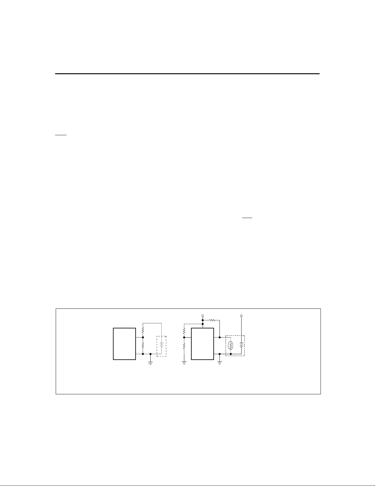
Battery Voltageand Temperature
Measurements
Battery voltage and temperature are monitored for
maximum allowable values. The voltage presented on
the battery sense input, BAT, should represent a
single-cell potential for the battery under charge. A
resistor-dividerratioof
RB1
= N - 1
RB2
is recommended to maintain the battery voltage within
the valid range, where N is the number of cells, RB1 is
the resistor connected to the positive battery terminal,
and RB2 is the resistor connected to the negative
battery terminal. See Figure 1.
Note: This resistor-divider network input impedance to
end-to-end should be at least 200kΩ and less than 1 MΩ.
-
A ground-referenced negative temperature coefficient
thermistor placed near the battery may be used as a lowcost temperature-to-voltage transducer. The temperature
sense voltage input at TS is developed using a resistorthermistor network between V
and VSS. See Figure 1.
CC
-
V
CC
RB1
BAT
bq2002C
BAT pin connection Thermistor connection
RB2
V
SS
NTC = negative temperature coefficient thermistor.
R3
R4
Mid-level
setting for TM
V
CC
TM
bq2002C
T
V
SS
PACK +
RT
S
N
T
C
Fg2002/C.eps
Figure 1. Voltage and Temperature Monitoring and TM Pin Configuration
2
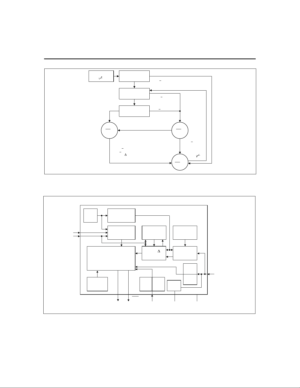
bq2002C
OSC
V
CC
Chip on
4.0V
V
TS
V
BAT
0.84V < V
BAT
/2
> V
CC
Fast
LED =
Low
V
BAT
VTS < VCC/2 or
PVD or - V or
Maximum Time Out
Clock
Phase
Generator
Battery Voltage
too High?
< 2V
Battery Voltage
too Low?
Battery
Temperature?
> 2V or
V
V
V
BAT
BAT
TS
V
> V
2V
>
BAT
< 0.84V
V
BAT
< V
V
CC
TS
> 0.84V and
< 2V and
/2
CC
/2
Figure 2. State Diagram
Trickle
LED =
Flash
Trickle
LED = Z
Charge
Pending
V
BAT
V
> 2V
BAT
2V
20
D
S
s
p
.e
C
02
TM
INH
Charge-Control
State Machine
Power-On
Reset
Timing
Control
Sample
History
PVD, - V
ALU
HTF
Check
CC
LED
Figure 3. Block Diagram
3
TCO
Check
TS
Power
Down
Voltage
Reference
A to D
Converter
LBAT
Check
MCV
Check
V
CC
V
SS
Bd2002CEG.eps
BAT
bq2002C
Fast ChargingVCC = 0 Fast Charging
CC Output
Charge initiated by application of power
Charge initiated by battery replacement
LED
Figure 4. Charge Cycle Phases
Starting ACharge Cycle
Either of two events starts a charge cycle (see Figure 4):
1.Applicationofpowerto V
2. Voltage at the BAT pin falling through the maximum
cell voltage V
MCV
where
V
If the battery is within the configured temperature and
voltage limits, the IC begins fast charge. The valid
battery voltage range is V
V
LBAT
The valid temperature range is V
V
HTF
If V
BAT
≤ V
LBAT
or VTS≤ V
or
CC
= 2V ±5%.
MCV
LBAT<VBAT<VMCV,
= 0.175 ∗ VCC±20%
TS>VHTF
= 0.6 ∗ VCC±5%.
, the IC enters the charge-
HTF
where
where
Pulse-Trickle
1s
See
Table 1
TD2002C1.eps
pending state. In this state pulse trickle charge is
applied to the battery and the LED flashes until the
voltage and temperature come into the allowed fast
charge range or V
≥ V
, the IC enters the Charge Complete/Battery
MCV
rises above V
BAT
. Anytime V
MCV
BAT
Absent state. In this state the LED is off and trickle
charge is applied to the battery until the next new
charge cycle begins.
Fast charge continues until termination by one or more of
the five possible termination conditions:
n
Peak voltage detection (PVD)
n
Negative delta voltage (-∆V)
n
Maximum voltage
n
Maximum temperature
n
Maximum time
Table 1. Fast-Charge Safety Time/Hold-Off Table
Typical
Corresponding
Fast-Charge
Rate TM Termination
Fast-
Charge
Time Limits
(minutes)
Typical PVD
and -∆V
Hold-Off
Time (seconds)
Pulse-
Trickle
Rate
C/2 Mid PVD 160 300 C/32 73 18.7
1C Low PVD 80 150 C/32 37 18.7
2C High -∆V 40 75 C/32 18 9.4
Notes: Typical conditions = 25°C, VCC= 5.0V
Mid = 0.5*V
CC
±0.5V
Tolerance on all timing is ±12%.
4
Pulse-
Trickle
Pulse Width
(ms)
Maximum
Synchronized
Sampling
Period
(seconds)

bq2002C
PVD and -∆VTermination
There are two modes for voltage termination, depend
ing on the state of TM. For -∆V (TM = high), if V
lower than any previously measured value by 12mV
±3mV, fast charge is terminated. For PVD (TM = low or
mid), a decrease of 2.5mV ±2.5mV terminates fast
charge. The PVD and -∆V tests are valid in the range
1V<V
BAT
<2V.
BAT
Synchronized Voltage Sampling
Voltagesampling at the BAT pin for PVD and -∆V termi
nation may be synchronized to an external stimulus
using the INH input. Low-high-low input pulses
between 100ns and 3.5ms in width must be applied at
the INH pin with a frequency greater than the “maxi
mum synchronized sampling period” set by the state of
the TM pin as shown in Table 1. Voltage is sampled on
the falling edge of such pulses. If the time between
pulses is greater than the synchronizing period, voltage
sampling “free-runs” at once every 17 seconds. A sample
is taken by averaging together voltage measurements
taken 57µs apart. The IC takes 32 measurements in
PVD mode and 16 measurements in -∆V mode. The
resulting sample periods (9.17 and 18.18ms, respectively) filter out harmonics centered around 55 and
109Hz. This technique minimizes the effect of any AC
line ripple that may feed through the power supply from
either 50 or 60Hz AC sources. If the INH input remains
high for more than 12ms, the voltage sample history
kept by the IC and used for PVD and -∆V termination
decisions is erased and a new history is started. Such a
reset is required when transitioning from free-running
to synchronized voltage sampling. The response of the
IC to pulses less than 100ns in width or between 3.5ms
and 12ms is indeterminate. The tolerance on all timing
is±12%.
Voltage Termination Hold-off
A hold-off period occurs at the start of fast charging.
During the hold-off time, the PVD and -∆V terminations
are disabled. This avoids premature termination on the
voltage spikes sometimes produced by older batteries
when fast-charge current is first applied. Maximum
voltage and temperature terminations are not affected
by the hold-off period.
Maximum Voltage, Temperature,and Time
Any time the voltage on the BAT pin exceeds the maxi
mum cell voltage, V
Maximum temperature termination occurs anytime the
voltage on the TS pin falls below the temperature cut-off
threshold V
TCO,
,fast charge is terminated.
MCV
where
= 0.5 ∗VCC±5%.
V
TCO
Maximum charge time is configured using the TM pin.
Time settings are available for corresponding charge
-
rates of C/2, 1C, and 2C. Maximum time-out termina
tion is enforced on the fast-charge phase,then reset, and
is
enforced again on the top-off phase, if selected. There is
no time limit on the trickle-charge phase.
Pulse-Trickle Charge
Pulse-trickle is used to compensate for self-discharge
while the battery is idle in the charger. The battery is
pulse-trickle charged by driving the CC pin active once
per second for the period specified in Table 1. This
results in a trickle rate of C/32.
TM Pin
The TM pin is a three-level pin used to select the
charge timer, top-off,voltage termination mode,trickle
rate, and voltage hold-off period options. Table 1
describes the states selected by the TM pin. The
mid-level selection input is developed by a resistor
divider between V
age on TM at V
CC
and ground that fixes the volt
CC
/2 ± 0.5V. See Figure 4.
Charge Status Indication
A fast charge in progress is uniquely indicated when the
LED
pin goes low. In the charge pending state, the LED
pin is driven low for 500ms, then to high-Z for 500ms.
The LED
conditions. Figure 2 outlines the state of the LED
during charge.
pin is driven to the high-Z state for all other
Charge Inhibit
Fast charge and top-off may be inhibited by using the
INH pin. When high, INH suspends all fast charge and
top-off activity and the internal charge timer. INH
freezes the current state of LED
removed. Temperature monitoring is not affected by the
INH pin. During charge inhibit, the bq2002C continues
to pulse-trickle charge the battery per the TM selection.
When INH returns low, charge control and the charge
timer resume from the point where INH became active.
until inhibit is
Low-Power Mode
The IC enters a low-power state when V
above the power-downthreshold(V
= VCC- (1V ±0.5V)
V
Both the CC pin and the LED
high-Z state. The operating current is reduced to less
than 1µA in this mode. When V
below V
new charge cycle begins.
PD
PD
, the IC pulse-trickle charges until the next
PD
pin are driven to the
BAT
BAT
) where
returns to a value
-
-
pin
is driven
5

bq2002C
Absolute Maximum Ratings
Symbol Parameter Minimum Maximum Unit Notes
V
CC
V
T
T
OPR
T
STG
T
SOLDER
T
BIAS
VCCrelative to V
SS
DC voltage applied on any pin
excluding V
relative to V
CC
SS
Operating ambient temperature 0 +70 °C Commercial
Storage temperature -40 +85 °C
Soldering temperature - +260 °C 10 sec max.
Temperature under bias -40 +85 °C
Note: Permanent device damage may occur if Absolute Maximum Ratings are exceeded. Functional opera
tion should be limited to the Recommended DC Operating Conditions detailed in this data sheet. Expo
sure to conditions beyond the operational limits for extended periods of time may affect device reliability.
-0.3 +7.0 V
-0.3 +7.0 V
-
-
DC Thresholds (T
= 0 to 70°C; V
A
CC
20%)
±
Symbol Parameter Rating Tolerance Unit Notes
V
TCO
Temperature cutoff 0.5*V
CC
±5%
V
VTS≤ V
inhibits/terminates
TCO
fast charge
V
HTF
High-temperature fault
0.6 ∗ V
CC
±5%
V
VTS≤ V
inhibits fast charge
HTF
start
V
MCV
Maximum cell voltage 2
±5%
V
V
≥ V
BAT
inhibits/terminates
MCV
fast charge
V
-∆V
LBAT
Minimum cell voltage
BAT input change for
0.175 ∗ V
-12
CC
±20%
±3
V
mV
V
BAT
≤ V
inhibits fast charge
LBAT
-∆V detection
PVD BAT input change for
-2.5
±2.5
mV
PVD detection
6

bq2002C
Recommended DC Operating Conditions (T
= 0 to 70°C)
A
Symbol Condition Minimum Typical Maximum Unit Notes
V
CC
V
DET
V
BAT
V
TS
V
IH
V
IM
V
IL
Supply voltage 4.0 5.0 6.0 V
-∆V, PVD detect voltage 1 - 2 V
Battery input 0 - V
Thermistor input 0.5 - V
CC
CC
V
VVTS< 0.5V prohibited
Logic input high 0.5 - - V INH
Logic input high V
Logic input mid
- 0.5 - - V TM
CC
V
CC
- 0.5
2
-
V
CC
05+ .
2
VTM
Logic input low - - 0.1 V INH
Logic input low - - 0.5 V TM
V
OL
V
PD
Logic output low - - 0.8 V LED, CC, IOL= 10mA
Power down VCC- 1.5 - VCC- 0.5 V V
BAT
V
≥
PD
max. powers
down bq2002C;
V
< VPDmin. =
BAT
normal operation.
I
CC
I
SB
I
OL
I
L
I
OZ
Supply current - - 500
Standby current - - 1
LED, CC sink 10 - - mA @VOL= VSS+ 0.8V
Input leakage - Output leakage in
high-Z state
Note: All voltages relative to VSS.
-5 - -
7
A Outputs unloaded,
µ
V
= 5.1V
CC
AVCC= 5.1V, V
µ
1
±
A INH, CC, V = VSSto V
µ
A LED,CC
µ
BAT
= V
PD
CC

bq2002C
Impedance
Symbol Parameter Minimum Typical Maximum Unit
R
BAT
R
TS
Battery input impedance 50 - - M
TS input impedance 50 - - M
Ω
Ω
Timing (T
Symbol Parameter Minimum Typical Maximum Unit Notes
d
FCV
Note: Typical is at TA= 25°C,VCC= 5.0V.
= 0 to +70°C; V
A
Time base variation -12 - 12 %
CC
10%)
±
8

bq2002C
8-Pin DIP(PN
E1
E
C
e
)
8-Pin PN(0.300" DIP
D
Dimension
A 0.160 0.180 4.06 4.57
A1 0.015 0.040 0.38 1.02
B 0.015 0.022 0.38 0.56
B1 0.055 0.065 1.40 1.65
A
A1
L
B1
C 0.008 0.013 0.20 0.33
D 0.350 0.380 8.89 9.65
E 0.300 0.325 7.62 8.26
E1 0.230 0.280 5.84 7.11
e 0.300 0.370 7.62 9.40
S
B
G
G 0.090 0.110 2.29 2.79
L 0.115 0.150 2.92 3.81
S 0.020 0.040 0.51 1.02
Min. Max. Min. Max.
)
Inches Millimeters
9

bq2002C
8-Pin SOIC Narrow (SN)
8-Pin SN(0.150" SOIC
Inches Millimeters
Dimension
A 0.060 0.070 1.52 1.78
A1 0.004 0.010 0.10 0.25
B 0.013 0.020 0.33 0.51
C 0.007 0.010 0.18 0.25
D 0.185 0.200 4.70 5.08
E 0.150 0.160 3.81 4.06
e 0.045 0.055 1.14 1.40
H 0.225 0.245 5.72 6.22
L 0.015 0.035 0.38 0.89
Min. Max. Min. Max.
)
10

Data Sheet Revision History
Change No. Page No. Description
1 All Revised format and outline of this data sheet
Note: Change 1 = Sept. 1997 B changes from Dec. 1995.
Ordering Information
bq2002C
PackageOption:
PN = 8-pin plastic DIP
SN = 8-pin narrow SOIC
bq2002C
Device:
bq2002C Fast-ChargeIC
11

IMPORTANT NOTICE
T exas Instruments and its subsidiaries (TI) reserve the right to make changes to their products or to discontinue
any product or service without notice, and advise customers to obtain the latest version of relevant information
to verify, before placing orders, that information being relied on is current and complete. All products are sold
subject to the terms and conditions of sale supplied at the time of order acknowledgement, including those
pertaining to warranty, patent infringement, and limitation of liability.
TI warrants performance of its semiconductor products to the specifications applicable at the time of sale in
accordance with TI’s standard warranty. Testing and other quality control techniques are utilized to the extent
TI deems necessary to support this warranty . Specific testing of all parameters of each device is not necessarily
performed, except those mandated by government requirements.
CERTAIN APPLICATIONS USING SEMICONDUCT OR PRODUCTS MAY INVOLVE POTENTIAL RISKS OF
DEATH, PERSONAL INJURY, OR SEVERE PROPERTY OR ENVIRONMENTAL DAMAGE (“CRITICAL
APPLICATIONS”). TI SEMICONDUCTOR PRODUCTS ARE NOT DESIGNED, AUTHORIZED, OR
WARRANTED TO BE SUITABLE FOR USE IN LIFE-SUPPORT DEVICES OR SYSTEMS OR OTHER
CRITICAL APPLICA TIONS. INCLUSION OF TI PRODUCTS IN SUCH APPLICATIONS IS UNDERST OOD TO
BE FULLY AT THE CUSTOMER’S RISK.
In order to minimize risks associated with the customer’s applications, adequate design and operating
safeguards must be provided by the customer to minimize inherent or procedural hazards.
TI assumes no liability for applications assistance or customer product design. TI does not warrant or represent
that any license, either express or implied, is granted under any patent right, copyright, mask work right, or other
intellectual property right of TI covering or relating to any combination, machine, or process in which such
semiconductor products or services might be or are used. TI’s publication of information regarding any third
party’s products or services does not constitute TI’s approval, warranty or endorsement thereof.
Copyright 1999, Texas Instruments Incorporated
 Loading...