

Page 1

User's Guide
SLAU806–October 2019
BP-DAC11001EVM
This user’s guide describes the characteristics, operation, and use of the BP-DAC11001 evaluation
module (EVM) BoosterPack™ plug-in module. This EVM is designed to evaluate the performance of the
DAC11001 buffered voltage output DAC in a variety of configurations. Throughout this document, the
terms evaluation board, evaluation module, and EVM are synonymous with the BP-DAC11001EVM. This
document includes a schematic, reference printed-circuit board (PCB) layouts, and a complete bill of
materials.
Contents
1 Overview ..................................................................................................................... 3
1.1 Kit Contents ......................................................................................................... 3
1.2 Related Documentation from Texas Instruments .............................................................. 3
2 System Setup ................................................................................................................ 4
2.1 Software Setup ..................................................................................................... 4
2.2 Hardware Setup .................................................................................................... 6
3 Detailed Description ......................................................................................................... 8
3.1 Hardware Description ............................................................................................. 8
3.2 Software Description ............................................................................................. 10
4 Schematic, PCB Layout, and Bill of Materials.......................................................................... 16
4.1 BP-DAC11001EVM Schematic ................................................................................. 16
4.2 PCB Layout ........................................................................................................ 20
4.3 BP-DAC11001EVM Bill of Materials............................................................................ 23
List of Figures
1 BP-DAC11001EVM Software Setup ...................................................................................... 4
2 Software Installation Path .................................................................................................. 4
3 Launchpad Setup ............................................................................................................ 5
4 TI Cloud Agent Installation ................................................................................................. 5
5 Hardware Setup.............................................................................................................. 6
SLAU806–October 2019
Submit Documentation Feedback
Copyright © 2019, Texas Instruments Incorporated
BP-DAC11001EVM
1
Page 2

www.ti.com
6 BP-DAC11001EVM Hardware Block Diagram........................................................................... 8
7 Launchpad Interface Pinout................................................................................................ 9
8 BP-DAC11001EVM GUI Location........................................................................................ 10
9 GUI Connection Detection ................................................................................................ 10
10 Software Home Page...................................................................................................... 11
11 Setup Page.................................................................................................................. 12
12 DAC Quick-Start Page: Basic DAC Tab ................................................................................ 13
13 Register Map Page ........................................................................................................ 14
14 Register Page Options .................................................................................................... 14
15 Collateral Page ............................................................................................................. 15
16 Schematic Page 1.......................................................................................................... 16
17 Schematic Page 2.......................................................................................................... 17
18 Schematic Page 3.......................................................................................................... 18
19 Schematic Page 4.......................................................................................................... 19
20 PCB Components: Top Overlay.......................................................................................... 20
21 PCB Components: Bottom Overlay...................................................................................... 20
22 PCB Layout: Top Layer ................................................................................................... 21
23 PCB Layout: Ground Plane............................................................................................... 21
24 PCB Layout: Power Plane ................................................................................................ 22
25 PCB Layout: Bottom Layer................................................................................................ 22
1 Kit Contents .................................................................................................................. 3
2 Required Components Not Included With Kit............................................................................ 3
3 Related Documentation ..................................................................................................... 3
4 BP-DAC11001EVM Power Supply Inputs................................................................................ 7
5 BP-DAC11001EVM Jumper Settings ..................................................................................... 7
6 BP-DAC11001EVM Bill of Materials .................................................................................... 23
Trademarks
BoosterPack is a trademark of Texas Instruments Inc.
Windows is a trademark of Microsoft Corporation.
All other trademarks are the property of their respective owners.
List of Tables
2
BP-DAC11001EVM
Copyright © 2019, Texas Instruments Incorporated
SLAU806–October 2019
Submit Documentation Feedback
Page 3
www.ti.com
1 Overview
The BP-DAC11001EVM is an easy-to-use platform to evaluate the functionality and performance of the
DAC11001 device. The DAC11001 is a highly accurate, low-noise, voltage-output, single-channel, digitalto-analog converter (DAC). The DAC11001 is specified monotonic by design, and offers excellent linearity
of less than 4 LSB (max) across all ranges.
The unbuffered voltage output offers low-noise performance (7 nV/√Hz) in combination with fast settling
time (1 μs), making this device an excellent choice for low-noise, high-speed applications. The DAC11001
integrates an enhanced deglitch circuit with range- and code-independent symmetrical ultra-low glitch (1.5
nV-s) to enable clean waveform ramps with ultra-low harmonic distortion (THD).
The DAC11001 device incorporates a power-on-reset (POR) circuit so that the DAC powers on with
known values in the registers. With external references, DAC output ranges from V
achieved, including asymmetric output ranges.
The DAC11001 uses a versatile 4–wire serial interface that operates at clock rates of up to 50 MHz. The
DAC11001 is specified over the industrial temperature range of –40°C to +125°C.
The EVM provides the GPIO and SPI programming interface using a PC-based graphical user interface
(GUI). This EVM requires the MSP-EXP432E401Y Launchpad for interfacing with the PC-based GUI.
1.1 Kit Contents
Table 1 details the contents of the EVM kit. Contact the TI Product Information Center nearest you if any
component is missing. TI highly recommends that the user verify latest versions of the related software at
the TI website, www.ti.com.
REFPF
to V
REFNF
Overview
can be
Table 1. Kit Contents
Item Quantity
BP-DAC11001EVM BoosterPack 1
Table 2. Required Components Not Included With Kit
Item Quantity
MSP-EXP432E401Y Launchpad 1
The MSP-EXP432E401Y Launchpad can be purchased from the MSP432E401Y tool folder on
www.ti.com.
1.2 Related Documentation from Texas Instruments
The following document provides information regarding Texas Instruments integrated circuits used in the
assembly of the BP-DAC11001EVM. This user's guide is available from the TI web site under literature
number SLAU806. Any letter appended to the literature number corresponds to the document revision that
is current at the time of the writing of this document. Newer revisions may be available from the TI web
site at http://www.ti.com/, or call the Texas Instruments Literature Response Center at (800) 477-8924 or
the Product Information Center at (972) 644-5580. When ordering, identify the document by both title and
literature number.
Table 3. Related Documentation
Document Literature Number
DAC11001 product data sheet SLASEL0
SLAU806–October 2019
Submit Documentation Feedback
Copyright © 2019, Texas Instruments Incorporated
BP-DAC11001EVM
3
Page 4

System Setup
2 System Setup
2.1 Software Setup
This section provides the procedure for EVM software installation.
2.1.1 Software Installation
The EVM software is compatible with the Windows™ 7, 8, and 10 operating systems. The software is
available on the product folder, and can also be found in the GUI Composer Gallery. Search for BP-
DAC11001EVM in the GUI Composer Gallery. Use the down arrow symbol to download the software.
There are two downloads: BP-DAC11001EVM GUI and GUI Composer Runtime. Either download both, or
just download the EVM GUI; the runtime file can be downloaded through the EVM GUI during installation.
The software can also be run online; however, only after the firmware and driver are upgraded. After the
software is downloaded onto the PC, navigate to the download folder, and run the BP-DAC11001EVM
software executable, as shown in Figure 1.
www.ti.com
Figure 1. BP-DAC11001EVM Software Setup
When the BP-DAC11001EVM software is launched, an installation dialog window opens and prompts the
user to select an installation directory. If left unchanged, the software location defaults to C:\Program Files
(x86)\Texas Instruments\BP-DAC11001 EVM, as shown in Figure 2. If there is no previous installation of
the GUI Composer Runtime application, the installer also requests for an automatic download from the
web. Select either Install from Web to download and install from the web, or Install from PC and provide
the path to the local file that is already downloaded. The runtime executable also installs the USB drivers,
unless the drivers are already installed.
The software installation automatically copies the required files and drivers to the local machine.
Figure 2. Software Installation Path
4
BP-DAC11001EVM
Copyright © 2019, Texas Instruments Incorporated
SLAU806–October 2019
Submit Documentation Feedback
Page 5
3 42
Remove
Jumper
Mount
Jumper
1
www.ti.com
2.1.2 Launchpad Firmware Upgrade
Before using the software for the first time, upgrade the firmware for the launchpad. The firmware is
programmed to the launchpad using the online tool, UniFlash. This link is also provided on the Setup page
of the GUI. After unzipping the install_image_BP-DAC11001EVM.zip file, the firmware bin file is found at
<Download Directory>\BP-DAC11001EVM_1.0.1_installer_win\install_image_BP-DAC11001EVM\BPDAC11001EVM\firmware\acctrl.bin.
Follow the step-by-step procedure below to upgrade the firmware and install the device drivers
successfully:
1. Remove jumper JP6 on the launchpad, as shown in step 1 of Figure 3.
System Setup
Figure 3. Launchpad Setup
2. Mount the jumper on 5V-OTG. Retain the jumper on 5V-XDS, as shown in step 1 of Figure 3.
3. Connect the USB cable to the port on the XDS110 side of the board, as shown in step 2 of Figure 3.
4. Connect the USB cable to PC and open UniFlash. Click on Start Now in the Detect Device section.
5. If the GUI Composer framework is being installed for the first time on the PC, the browser extension
and the TI Cloud Agent must also be installed. Follow the 2-step installation flow prompted on the web
page, as shown in Figure 4
6. Press the Refresh or Finish button after the installation is complete. This action should detect the
launchpad.
7. Press Start and browse for <Download Directory>\BP-
DAC11001EVM_1.0.1_installer_win\install_image_BP-DAC11001EVM.\BPDAC11001EVM\firmware\acctrl.bin. Press Load Image followed by Verify Image.
SLAU806–October 2019
Submit Documentation Feedback
Figure 4. TI Cloud Agent Installation
Copyright © 2019, Texas Instruments Incorporated
BP-DAC11001EVM
5
Page 6
System Setup
2.2 Hardware Setup
This section provides the overall system setup for the EVM. The hardware setup contains the MSPEXP432E401Y launchpad and the BP-DAC11001EVM. A PC runs the software that provides an interface
to the BP-DAC11001EVM through the launchpad.
The BP-DAC11001EVM requires external power supplies, as described later in this document. The 3.3-V
and 5-V power supplies from the launchpad can be used for IOVDD and DVDD for the DAC, respectively,
using jumper options. The launchpad generates the digital signals used to communicate with the EVM
board.
Figure 5 displays the hardware setup.
www.ti.com
Figure 5. Hardware Setup
6
BP-DAC11001EVM
Copyright © 2019, Texas Instruments Incorporated
SLAU806–October 2019
Submit Documentation Feedback
Page 7
www.ti.com
2.2.1 Power Configurations and Jumper Settings
The BP-DAC11001EVM provides electrical connections to the device supply pins. The connectors and
optional configurations are shown in Table 4, and Table 5 shows the EVM jumper settings.
Table 4. BP-DAC11001EVM Power Supply Inputs
BP-DAC11001EVM Connector Supply Name Voltage Range Test Point
J12 VCC 5 V to 15 V TP21
J13 VSS –5 V to –15 V TP24
J14 VDD 4.5 V to 5.5 V TP25
J15 VIO 2.7 V to 5.5 V (Option: 3V3 on the launchpad) TP26
J17 GND 0 V TP27
J18 REF_PWR 5.3 V to 5.5 V TP33
J19 REFGND 0 V TP34
Table 5. BP-DAC11001EVM Jumper Settings
Jumper Description Default Position Alternative Position
J1 2x gain configuration None 1-2 or 2-3
J2 Output amplifier feedback configuration
J4 LDAC pull-down None 1-2: LDAC tied low
J5 CLR pull-down None 1-2: CLR tied low
J7 DAC output to load circuit connection
J8 AGND-OUT to FILTGND connection None 1-2: AGND-OUT and FILTGND shorted
J11 DVDD connection 2-3: DVDD from AEVM_5V0 1-2: DVDD from VDD
J16 IOVDD connection 2-3: IOVDD from AEVM_3V3 1-2: IOVDD from VIO
J20 REF_PWR connection
J25 Reference filter bypass None 1-2: Bypass reference filter
J26 Reference source selection 2-3: Onboard reference 1-2: External reference (3 V to 10 V)
J30 REFGND connection 2-3: Through ground buffer 1-2: Do not use on the Rev A PCB
J31 Negative reference selection 2-3: Inverted reference source 1-2: Tied to ground (unipolar output mode)
System Setup
1-2, 3-4: external resistor and
capacitor connection
None 1-2: DAC output to auxiliary circuit; 2-3: DAC
2-3: REF_PWR from J18 1-2: REF_PWR from VCC. Make sure VCC
5-6, 7-8: embedded resistor connection
output to filter input
is < 6 V before using this option.
2.2.2 Connecting the Hardware
After the launchpad firmware is upgraded as described in Section 2.1.2, and power and jumper
configurations done as per Section 2.2.1, the BP-DAC11001EVM and the launchpad can be connected as
shown in Figure 5. Connect the USB cable from the lauchpad OTG USB port (U7) to the PC.
2.2.3 Electrostatic Discharge Caution
Many of the components on the BP-DAC11001EVM and the launchpad are susceptible to damage by
electrostatic discharge (ESD). Observe proper ESD handling precautions when unpacking and handling
the EVM, including the use of a grounded wrist strap at an approved ESD workstation.
SLAU806–October 2019
Submit Documentation Feedback
Copyright © 2019, Texas Instruments Incorporated
BP-DAC11001EVM
7
Page 8
DAC110 01
RC
FILTER
REF625 0
EXTERNAL
REFEREN CE
REFP
REFN
REF_PWR
REFGN D
AGND
REF_VCC
REF_VSS
AGND
DGND
OUT_VCC OUT_VSS
AGND -OUT
BUFFERE D
DAC
OUTPU T
SW
FILTGND
FILT_VCC FILT_ VSS
FILTER1
FILTER2
AUXGND
VCC VSS VDD VIO
DGNDAGND
INTERF ACE FOR
AUXILIAR Y
CIRCU IT
VREFP VREFN
VCCVSS
VDD
VIOREF_PWR
REFGN D AGND
VCC VSS DVDD IOVD D
AVDD
EXTERNAL
LDAC
SPI
DGND
LAUNC HPAD
INTERF ACE
AEVM_3V 3
AEVM_5V 0
VDD
IOVDD
VDD
DVDD
VDD D VDD
Detailed Description
3 Detailed Description
3.1 Hardware Description
The following subsections provide detailed information on the EVM hardware and jumper configuration
settings.
3.1.1 Theory of Operation
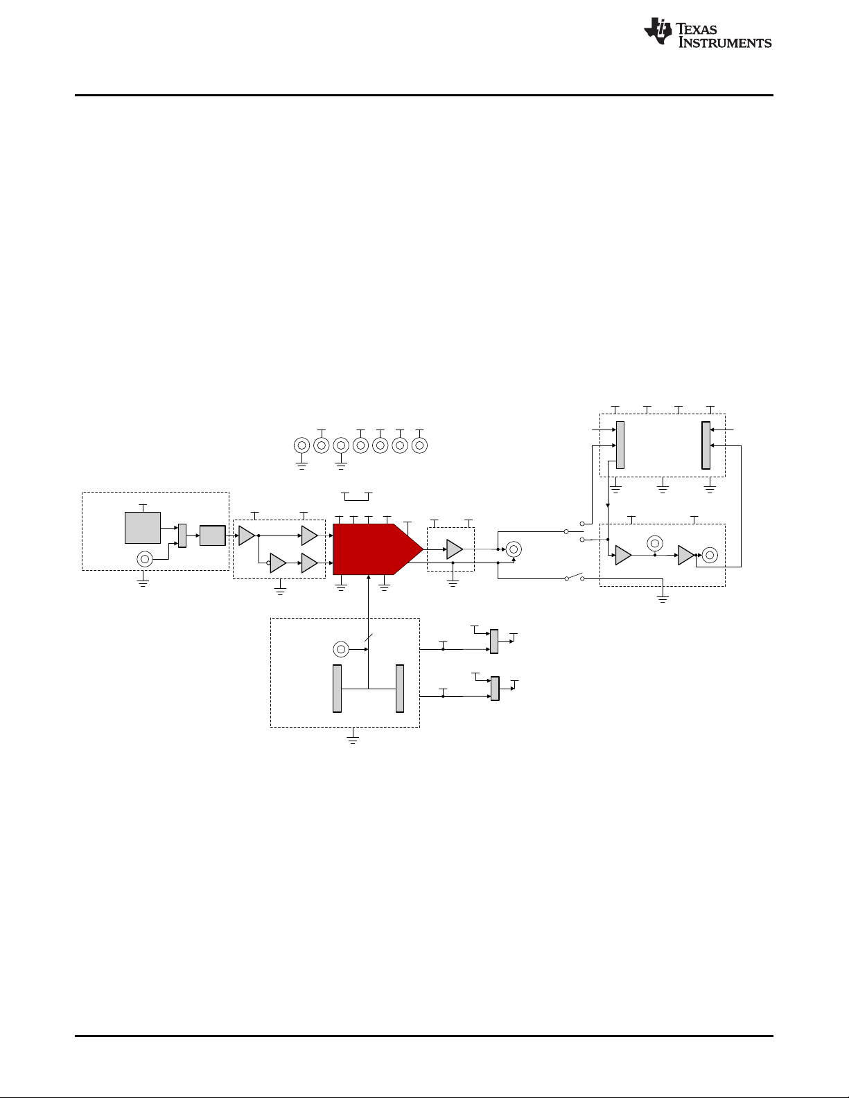
The block diagram of the BP-DAC11001EVM board is displayed in Figure 6. The dotted lines indicate
different power and ground domains. All grounds are shorted together using single-point shorts. The EVM
board connects to the launchpad with the BoosterPack connectors. There is an onboard reference, using
the REF6250, that generates a 5-V voltage reference, that in turn is converted to 5-V and –5-V reference
inputs for the DAC. There is an option for an external reference using connectors J27 and J28. Both J27
and J28 form a force-sense pair that eliminate cable losses while connected to external reference
sources. The DAC output is provided on J3. Jumper J2 provides various feedback options for the output
amplifier. The DAC output can be taken through two-stage, second-order filters using connectors J7 and
J8. There is an option to interface an external circuit using auxiliary connectors J23 and J24.
www.ti.com
Figure 6. BP-DAC11001EVM Hardware Block Diagram
8
BP-DAC11001EVM
Copyright © 2019, Texas Instruments Incorporated
SLAU806–October 2019
Submit Documentation Feedback
Page 9
1
2
3
4
5
6
7
8
9
10
20
19
18
17
16
15
14
13
12
11
3v3
LDAC
SCLK
GND
21
22
23
24
25
26
27
28
29
30
40
39
38
37
36
35
34
33
32
31
5v
GND
CLR
Pin aligns with BoosterPack pinout standard
SYNC
SDO
SDIN
www.ti.com
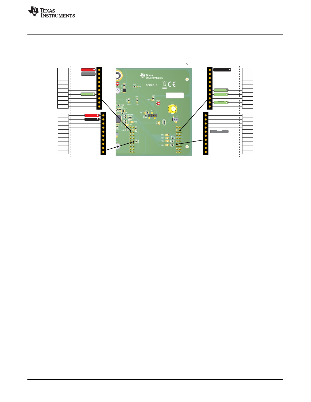
3.1.2 Signal Definition for the Launchpad Interface
The BP-DAC11001EVM interfaces with the launchpad through connectors J9 and J10. The pin definitions
are shown in Figure 7.
Figure 7. Launchpad Interface Pinout
Detailed Description
SLAU806–October 2019
Submit Documentation Feedback
Copyright © 2019, Texas Instruments Incorporated
BP-DAC11001EVM
9
Page 10

Detailed Description
3.2 Software Description
This section describes the features of the BP-DAC11001EVM software, and discusses how to use these
features. The software provides basic control of all the registers and functions of the DAC11001 device.
3.2.1 Starting the Software
To launch the software, locate the Texas Instruments folder in the All Programs menu, and select the BPDAC11001EVM icon, as shown in Figure 8.
www.ti.com
Figure 8. BP-DAC11001EVM GUI Location
Figure 9 shows that if the launchpad connector is connected correctly, the status bar at the bottom of the
screen displays Hardware Connected. If the launchpad is not properly connected or not connected at all,
the status bar displays Hardware not connected. In case the Hardware not connected status persists even
after the hardware is connected, go to Options → Serial Port, and change the port to the other available
port with the (Texas Instruments) or ACCtrl tag. One of the two ports with these tags will connect to the
hardware.
Figure 9. GUI Connection Detection
10
BP-DAC11001EVM
Copyright © 2019, Texas Instruments Incorporated
SLAU806–October 2019
Submit Documentation Feedback
Page 11

www.ti.com
3.2.2 Software Features
The BP-DAC11001EVM incorporates interactive functions that help configure the DAC11001 device.
These functions are built into several GUI pages, as shown in the following sections. The Menu button
allows the user to switch between the pages, with each page representing a feature of the software.
3.2.2.1 Home Page
The Home page, shown in Figure 10, provides the basic information and navigation to other pages. Click
on Learn More... to get more information on the device.
Detailed Description
SLAU806–October 2019
Submit Documentation Feedback
Figure 10. Software Home Page
Copyright © 2019, Texas Instruments Incorporated
BP-DAC11001EVM
11
Page 12

Detailed Description
3.2.2.2 Setup Page
The Setup page, shown in Figure 11, guides the user to perform a one-time firmware upgrade for the
launchpad.
www.ti.com
Figure 11. Setup Page
12
BP-DAC11001EVM
Copyright © 2019, Texas Instruments Incorporated
SLAU806–October 2019
Submit Documentation Feedback
Page 13

www.ti.com
3.2.2.3 DAC Quick-Start Page
The DAC Quick-Start page provides the functions to quickly get started with the EVM. The basic
initialization settings are meant for basic dc operation; whereas, the advanced settings are meant for ac
functionality, such as settling time and total harmonic distortion (THD). Write a decimal code to the DAC
output input box to get the corresponding analog output.
Detailed Description
Figure 12. DAC Quick-Start Page: Basic DAC Tab
SLAU806–October 2019
Submit Documentation Feedback
Copyright © 2019, Texas Instruments Incorporated
BP-DAC11001EVM
13
Page 14

Detailed Description
3.2.2.4 Register Map Page
The Register Map page, shown in Figure 13, allows the user to access low-level communication directly
with the DAC11001 registers. Selecting a register on the Register Map list shows a description of the
values in that register, as well as information on the register address, default value, size, and current
value. Values are read from and written to the registers by writing to the Value or bit field of the GUI.
www.ti.com
Figure 13. Register Map Page
There are some configuration lists and action buttons provided on the Register Map page. To store the
values of the register map locally, press the Save Registers button under the File menu option.
Additionally, recall and load the stored configuration files through the Load Registers button. Other options
selectable by the user are the Auto Read Interval, Read Register, Read All Registers, Write Register,
Write All Registers, and Update Mode buttons. These buttons are displayed in Figure 14. The Write
Register and Write All Registers buttons are enabled only with Deferred update mode. Deferred mode
initiates a write operation only when the Write Register or the Write All Registers button is pressed. By
default, the Immediate update mode is selected for the Register Map page write operations.
Figure 14. Register Page Options
14
BP-DAC11001EVM
Copyright © 2019, Texas Instruments Incorporated
SLAU806–October 2019
Submit Documentation Feedback
Page 15

www.ti.com
3.2.2.5 Collateral Page
This page shown in Figure 15 provides links for all the collateral on the DAC11001 device.
Detailed Description
Figure 15. Collateral Page
SLAU806–October 2019
Submit Documentation Feedback
Copyright © 2019, Texas Instruments Incorporated
BP-DAC11001EVM
15
Page 16

Schematic, PCB Layout, and Bill of Materials
4 Schematic, PCB Layout, and Bill of Materials
This section contains the complete bill of materials and schematic diagram for the BP-DAC11001EVM.
4.1 BP-DAC11001EVM Schematic
www.ti.com
16
BP-DAC11001EVM
Figure 16. Schematic Page 1
SLAU806–October 2019
Submit Documentation Feedback
Copyright © 2019, Texas Instruments Incorporated
Page 17

www.ti.com
Schematic, PCB Layout, and Bill of Materials
SLAU806–October 2019
Submit Documentation Feedback
Figure 17. Schematic Page 2
Copyright © 2019, Texas Instruments Incorporated
BP-DAC11001EVM
17
Page 18

Schematic, PCB Layout, and Bill of Materials
www.ti.com
18
BP-DAC11001EVM
Figure 18. Schematic Page 3
SLAU806–October 2019
Submit Documentation Feedback
Copyright © 2019, Texas Instruments Incorporated
Page 19

www.ti.com
Schematic, PCB Layout, and Bill of Materials
SLAU806–October 2019
Submit Documentation Feedback
Figure 19. Schematic Page 4
Copyright © 2019, Texas Instruments Incorporated
BP-DAC11001EVM
19
Page 20

Schematic, PCB Layout, and Bill of Materials
4.2 PCB Layout
Figure 20 through Figure 25 show the layout details of the BP-DAC11001EVM board.
Figure 20. PCB Components: Top Overlay
www.ti.com
20
BP-DAC11001EVM
Figure 21. PCB Components: Bottom Overlay
Copyright © 2019, Texas Instruments Incorporated
SLAU806–October 2019
Submit Documentation Feedback
Page 21

www.ti.com
Schematic, PCB Layout, and Bill of Materials
Figure 22. PCB Layout: Top Layer
SLAU806–October 2019
Submit Documentation Feedback
Figure 23. PCB Layout: Ground Plane
Copyright © 2019, Texas Instruments Incorporated
BP-DAC11001EVM
21
Page 22

Schematic, PCB Layout, and Bill of Materials
Figure 24. PCB Layout: Power Plane
www.ti.com
22
BP-DAC11001EVM
Figure 25. PCB Layout: Bottom Layer
Copyright © 2019, Texas Instruments Incorporated
SLAU806–October 2019
Submit Documentation Feedback
Page 23

www.ti.com
4.3 BP-DAC11001EVM Bill of Materials
Table 6 lists the EVM bill of materials (BOM).
Schematic, PCB Layout, and Bill of Materials
Table 6. BP-DAC11001EVM Bill of Materials
Designator Quantity Value Description Package Reference Part Number Manufacturer Alternate Part
!PCB1 1 Printed Circuit Board DC026 Any
C1, C47, C55 3 100pF CAP, CERM, 100 pF, 50 V,
C2, C4, C7, C8, C9, C10,
C13, C16, C18, C28, C35,
C36, C39, C40, C44, C46,
C50, C51, C53, C54, C56,
C57, C58, C59
C5, C6 2 10uF CAP, CERM, 10 uF, 10 V,
C11, C12, C14, C15, C17,
C19, C20, C21, C22, C23,
C29, C30
C24, C25, C26, C27, C31,
C42, C60, C61
C32, C34 2 0.01uF CAP, CERM, 0.01 uF, 50 V,
C33, C37, C38 3 2700pF CAP, CERM, 2700 pF, 25 V,
C41, C43, C45 3 1uF CAP,Film, 1 uF, 16 V, +/-
D1, D2, D3, D4, D5, D6, D7,
D8, D9
H1, H2, H3, H4 4 MACHINE SCREW PAN
J1, J7, J11, J16, J20, J26,
J30, J31
J2 1 Header, 2.54mm, 4x2, Gold,
J3, J6, J21, J22, J27, J28,
J29
J4, J5, J8, J25 4 Header, 100mil, 2x1, Gold
J9, J10 2 Receptacle, 2.54mm, 10x2,
J12, J13, J14, J15, J17,
J18, J19
J23, J24 2 Receptacle, 100mil, 10x1,
24 0.1uF CAP, CERM, 0.1 uF, 50 V,
12 1uF CAP, CERM, 1 uF, 50 V, +/-
8 10uF CAP, CERM, 10 uF, 50 V,
9 100V Diode, Schottky, 100 V, 1 A,
8 Header, 100mil, 3x1, Gold,
7 Connector, SMA, TH SMA 142-0701-231 Cinch Connectivity
7 Standard Banana Jack,
+/- 5%, C0G/NP0, 0603
+/- 10%, X7R, 0603
+/- 20%, X5R, 0603
10%, X7R, AEC-Q200
Grade 1, 0805
+/- 10%, X7S, AEC-Q200
Grade 1, 1210
+/- 5%, C0G/NP0, 0603
+/- 5%, C0G/NP0, 0805
20%, 1210 SMD
AEC-Q101, SOD-123W
PHILLIPS 4-40
SMT
SMT
with Tin Tail, SMT
Tin, TH
Uninsulated, 5.5mm
Tin, TH
0603 885012006057 Wurth Elektronik
0603 GRM188R71H104KA93D MuRata
0603 C1608X5R1A106M080AC TDK
0805 CGA4J3X7R1H105K125AB TDK
1210 CGA6P3X7S1H106K250AB TDK
0603 GRM1885C1H103JA01D MuRata
0805 08053A272JAT2A AVX
1210 ECPU1C105MA5 Panasonic
SOD-123W PMEG10010ELRX Nexperia
Machine Screw, 4-40, 1/4
inch
Samtec_TSM-103-01-X-SV TSM-103-01-L-SV Samtec
Header, 2.54mm, 4x2, SMT TSM-104-01-L-DV Samtec
2x1 Header TSM-102-01-L-SV Samtec
Receptacle, 2.54mm, 10x2,THESQ-110-14-T-D Samtec
Keystone_575-4 575-4 Keystone
Receptacle, 10x1, 100mil,
Tin
MSSS 440 0025 PH B and F Fastener
Supply
PPTC101LFBN-RC Sullins Connector
Solutions
Number
Alternate
Manufacturer
SLAU806–October 2019
Submit Documentation Feedback
Copyright © 2019, Texas Instruments Incorporated
BP-DAC11001EVM
23
Page 24

Schematic, PCB Layout, and Bill of Materials
Table 6. BP-DAC11001EVM Bill of Materials (continued)
Designator Quantity Value Description Package Reference Part Number Manufacturer Alternate Part
L1, L2, L3, L4, L5, L6, L7,
L8, L9
LBL1 1 Thermal Transfer Printable
R4, R5, R11, R12, R13,
R15, R16, R46, R52, R54
R6 1 2.4k RES, 2.4 k, 0.05%, 0.1 W,
R7, R8, R9, R10 4 10.0k RES, 10.0 k, 1%, 0.1 W,
R14, R17, R18, R19, R20,
R21, R22, R23
R24, R25, R26, R27, R28,
R29, R30, R31, R32, R33,
R34, R35, R40
R36 1 2.49k RES, 2.49 k, 1%, 0.1 W,
R37 1 3.40k RES, 3.40 k, 1%, 0.1 W,
R38 1 866 RES, 866, 1%, 0.1 W, AEC-
R39 1 1.58k RES, 1.58 k, 1%, 0.1 W,
R41 1 0.51 RES,0.51, 1%, 0.1 W, AEC-
R42 1 1.00 RES,1.00, 1%, 0.1 W, 0603 0603 RC0603FR-071RL Yageo
R43, R51 2 22 RES, 22.0, 0.1%, 0.063 W,
R44 1 51k RES, 51 k, 5%, 0.1 W, AEC-
R47, R48 2 4.99k RES, 4.99 k, 0.1%, 0.125
R55, R56 2 1.00k RES, 1.00 k, 0.01%, 0.15
SH-JP1, SH-JP2, SH-JP3,
SH-JP4, SH-JP5, SH-JP6,
SH-JP7, SH-JP8, SH-JP9,
SH-JP10
TP6, TP21, TP24, TP25,
TP26, TP27, TP28, TP29,
TP30, TP31, TP32, TP33,
TP34, TP35, TP36, TP37,
TP38, TP39, TP40, TP41,
TP42
9 600 ohm Ferrite Bead, 600 ohm at
100 MHz, 2.1 A, 0805
Labels, 0.650" W x 0.200" H
- 10,000 per roll
10 0 RES, 0, 1%, 0.1 W, AEC-
Q200 Grade 0, 0603
AEC-Q200 Grade 0, 0603
0603
8 33 RES, 33, 5%, 0.1 W, AEC-
Q200 Grade 0, 0603
13 10 RES, 10, 5%, 0.1 W, AEC-
Q200 Grade 0, 0603
AEC-Q200 Grade 0, 0603
AEC-Q200 Grade 0, 0603
Q200 Grade 0, 0603
AEC-Q200 Grade 0, 0603
Q200 Grade 1, 0603
0603
Q200 Grade 0, 0603
W, 0805
W, 0603
10 1x2 Shunt, 100mil, Gold plated,
Black
21 Test Point, Compact, Red,THRed Compact Testpoint 5005 Keystone
0805 74279220601 Wurth Elektronik
PCB Label 0.650 x 0.200
inch
0603 RMCF0603ZT0R00 Stackpole Electronics
0603 RG1608N-242-W-T1 Susumu Co Ltd
0603 RC0603FR-0710KL Yageo
0603 CRCW060333R0JNEA Vishay-Dale
0603 CRCW060310R0JNEA Vishay-Dale
0603 CRCW06032K49FKEA Vishay-Dale
0603 CRCW06033K40FKEA Vishay-Dale
0603 CRCW0603866RFKEA Vishay-Dale
0603 CRCW06031K58FKEA Vishay-Dale
0603 ERJ-3RQFR51V Panasonic
0603 CPF0603B22RE1 TE Connectivity
0603 CRCW060351K0JNEA Vishay-Dale
0805 RT0805BRD074K99L Yageo America
0603 PLTU0603U1001LST5 Vishay-Dale
Shunt SNT-100-BK-G Samtec 969102-0000-DA 3M
THT-14-423-10 Brady
Inc
Number
www.ti.com
Alternate
Manufacturer
24
BP-DAC11001EVM
SLAU806–October 2019
Submit Documentation Feedback
Copyright © 2019, Texas Instruments Incorporated
Page 25

www.ti.com
Schematic, PCB Layout, and Bill of Materials
Table 6. BP-DAC11001EVM Bill of Materials (continued)
Designator Quantity Value Description Package Reference Part Number Manufacturer Alternate Part
U1 1 20-/18-/16-Bit, Low Noise,
Ultra Low Harmonic
Distortion, Fast Settling,
High-Voltage Output Digitalto-Analog Converters
(DACs), PFB0048A (TQFP-
48)
U2, U6, U7, U8, U9, U10 6 36-Volt, High-speed (45
MHz GBW and 150V/μs
SR), low-noise (4nV/√Hz)
RRO JFET operational
amplifier, D0008A (SOIC-8)
U3, U4 0 1.1 nV/rtHz Noise, Low
Power, Precision
Operational Amplifier, 4.5 to
36 V, -40 to 85 degC, 8-pin
SOIC (D8), Green (RoHS &
no Sb/Br)
U5 1 High-Precision Voltage
Reference with Integrated
High-Bandwidth Buffer,
DGK0008A (VSSOP-8)
C3, C52 0 100pF CAP, CERM, 100 pF, 50 V,
+/- 5%, C0G/NP0, 0603
C48, C49 0 10uF CAP, Film, 10 uF, 63 V, +/-
10%, TH
FID1, FID2, FID3 0 Fiducial mark. There is
nothing to buy or mount.
R1, R2, R3, R45, R49, R53 0 0 RES, 0, 1%, 0.1 W, AEC-
Q200 Grade 0, 0603
PFB0048A DAC11001APFB Texas Instruments
D0008A OPA828IDR Texas Instruments
D0008A OPA1611AID Texas Instruments
DGK0008A REF6250IDGKR Texas Instruments REF6250IDGKT Texas Instruments
0603 885012006057 Wurth Elektronik
18x17.5x9mm B32522C106K TDK
N/A N/A N/A
0603 RMCF0603ZT0R00 Stackpole Electronics
Inc
Number
Alternate
Manufacturer
SLAU806–October 2019
Submit Documentation Feedback
Copyright © 2019, Texas Instruments Incorporated
BP-DAC11001EVM
25
Page 26

STANDARD TERMS FOR EVALUATION MODULES
1. Delivery: TI delivers TI evaluation boards, kits, or modules, including any accompanying demonstration software, components, and/or
documentation which may be provided together or separately (collectively, an “EVM” or “EVMs”) to the User (“User”) in accordance
with the terms set forth herein. User's acceptance of the EVM is expressly subject to the following terms.
1.1 EVMs are intended solely for product or software developers for use in a research and development setting to facilitate feasibility
evaluation, experimentation, or scientific analysis of TI semiconductors products. EVMs have no direct function and are not
finished products. EVMs shall not be directly or indirectly assembled as a part or subassembly in any finished product. For
clarification, any software or software tools provided with the EVM (“Software”) shall not be subject to the terms and conditions
set forth herein but rather shall be subject to the applicable terms that accompany such Software
1.2 EVMs are not intended for consumer or household use. EVMs may not be sold, sublicensed, leased, rented, loaned, assigned,
or otherwise distributed for commercial purposes by Users, in whole or in part, or used in any finished product or production
system.
2 Limited Warranty and Related Remedies/Disclaimers:
2.1 These terms do not apply to Software. The warranty, if any, for Software is covered in the applicable Software License
Agreement.
2.2 TI warrants that the TI EVM will conform to TI's published specifications for ninety (90) days after the date TI delivers such EVM
to User. Notwithstanding the foregoing, TI shall not be liable for a nonconforming EVM if (a) the nonconformity was caused by
neglect, misuse or mistreatment by an entity other than TI, including improper installation or testing, or for any EVMs that have
been altered or modified in any way by an entity other than TI, (b) the nonconformity resulted from User's design, specifications
or instructions for such EVMs or improper system design, or (c) User has not paid on time. Testing and other quality control
techniques are used to the extent TI deems necessary. TI does not test all parameters of each EVM.
User's claims against TI under this Section 2 are void if User fails to notify TI of any apparent defects in the EVMs within ten (10)
business days after delivery, or of any hidden defects with ten (10) business days after the defect has been detected.
2.3 TI's sole liability shall be at its option to repair or replace EVMs that fail to conform to the warranty set forth above, or credit
User's account for such EVM. TI's liability under this warranty shall be limited to EVMs that are returned during the warranty
period to the address designated by TI and that are determined by TI not to conform to such warranty. If TI elects to repair or
replace such EVM, TI shall have a reasonable time to repair such EVM or provide replacements. Repaired EVMs shall be
warranted for the remainder of the original warranty period. Replaced EVMs shall be warranted for a new full ninety (90) day
warranty period.
WARNING
Evaluation Kits are intended solely for use by technically qualified,
professional electronics experts who are familiar with the dangers
and application risks associated with handling electrical mechanical
components, systems, and subsystems.
User shall operate the Evaluation Kit within TI’s recommended
guidelines and any applicable legal or environmental requirements
as well as reasonable and customary safeguards. Failure to set up
and/or operate the Evaluation Kit within TI’s recommended
guidelines may result in personal injury or death or property
damage. Proper set up entails following TI’s instructions for
electrical ratings of interface circuits such as input, output and
electrical loads.
NOTE:
EXPOSURE TO ELECTROSTATIC DISCHARGE (ESD) MAY CAUSE DEGREDATION OR FAILURE OF THE EVALUATION
KIT; TI RECOMMENDS STORAGE OF THE EVALUATION KIT IN A PROTECTIVE ESD BAG.
Page 27

3 Regulatory Notices:
3.1 United States
3.1.1 Notice applicable to EVMs not FCC-Approved:
FCC NOTICE: This kit is designed to allow product developers to evaluate electronic components, circuitry, or software
associated with the kit to determine whether to incorporate such items in a finished product and software developers to write
software applications for use with the end product. This kit is not a finished product and when assembled may not be resold or
otherwise marketed unless all required FCC equipment authorizations are first obtained. Operation is subject to the condition
that this product not cause harmful interference to licensed radio stations and that this product accept harmful interference.
Unless the assembled kit is designed to operate under part 15, part 18 or part 95 of this chapter, the operator of the kit must
operate under the authority of an FCC license holder or must secure an experimental authorization under part 5 of this chapter.
3.1.2 For EVMs annotated as FCC – FEDERAL COMMUNICATIONS COMMISSION Part 15 Compliant:
CAUTION
This device complies with part 15 of the FCC Rules. Operation is subject to the following two conditions: (1) This device may not
cause harmful interference, and (2) this device must accept any interference received, including interference that may cause
undesired operation.
Changes or modifications not expressly approved by the party responsible for compliance could void the user's authority to
operate the equipment.
FCC Interference Statement for Class A EVM devices
NOTE: This equipment has been tested and found to comply with the limits for a Class A digital device, pursuant to part 15 of
the FCC Rules. These limits are designed to provide reasonable protection against harmful interference when the equipment is
operated in a commercial environment. This equipment generates, uses, and can radiate radio frequency energy and, if not
installed and used in accordance with the instruction manual, may cause harmful interference to radio communications.
Operation of this equipment in a residential area is likely to cause harmful interference in which case the user will be required to
correct the interference at his own expense.
www.ti.com
FCC Interference Statement for Class B EVM devices
NOTE: This equipment has been tested and found to comply with the limits for a Class B digital device, pursuant to part 15 of
the FCC Rules. These limits are designed to provide reasonable protection against harmful interference in a residential
installation. This equipment generates, uses and can radiate radio frequency energy and, if not installed and used in accordance
with the instructions, may cause harmful interference to radio communications. However, there is no guarantee that interference
will not occur in a particular installation. If this equipment does cause harmful interference to radio or television reception, which
can be determined by turning the equipment off and on, the user is encouraged to try to correct the interference by one or more
of the following measures:
• Reorient or relocate the receiving antenna.
• Increase the separation between the equipment and receiver.
• Connect the equipment into an outlet on a circuit different from that to which the receiver is connected.
• Consult the dealer or an experienced radio/TV technician for help.
3.2 Canada
3.2.1 For EVMs issued with an Industry Canada Certificate of Conformance to RSS-210 or RSS-247
Concerning EVMs Including Radio Transmitters:
This device complies with Industry Canada license-exempt RSSs. Operation is subject to the following two conditions:
(1) this device may not cause interference, and (2) this device must accept any interference, including interference that may
cause undesired operation of the device.
Concernant les EVMs avec appareils radio:
Le présent appareil est conforme aux CNR d'Industrie Canada applicables aux appareils radio exempts de licence. L'exploitation
est autorisée aux deux conditions suivantes: (1) l'appareil ne doit pas produire de brouillage, et (2) l'utilisateur de l'appareil doit
accepter tout brouillage radioélectrique subi, même si le brouillage est susceptible d'en compromettre le fonctionnement.
Concerning EVMs Including Detachable Antennas:
Under Industry Canada regulations, this radio transmitter may only operate using an antenna of a type and maximum (or lesser)
gain approved for the transmitter by Industry Canada. To reduce potential radio interference to other users, the antenna type
and its gain should be so chosen that the equivalent isotropically radiated power (e.i.r.p.) is not more than that necessary for
successful communication. This radio transmitter has been approved by Industry Canada to operate with the antenna types
listed in the user guide with the maximum permissible gain and required antenna impedance for each antenna type indicated.
Antenna types not included in this list, having a gain greater than the maximum gain indicated for that type, are strictly prohibited
for use with this device.
2
Page 28

www.ti.com
3.3 Japan
Concernant les EVMs avec antennes détachables
Conformément à la réglementation d'Industrie Canada, le présent émetteur radio peut fonctionner avec une antenne d'un type et
d'un gain maximal (ou inférieur) approuvé pour l'émetteur par Industrie Canada. Dans le but de réduire les risques de brouillage
radioélectrique à l'intention des autres utilisateurs, il faut choisir le type d'antenne et son gain de sorte que la puissance isotrope
rayonnée équivalente (p.i.r.e.) ne dépasse pas l'intensité nécessaire à l'établissement d'une communication satisfaisante. Le
présent émetteur radio a été approuvé par Industrie Canada pour fonctionner avec les types d'antenne énumérés dans le
manuel d’usage et ayant un gain admissible maximal et l'impédance requise pour chaque type d'antenne. Les types d'antenne
non inclus dans cette liste, ou dont le gain est supérieur au gain maximal indiqué, sont strictement interdits pour l'exploitation de
l'émetteur
3.3.1 Notice for EVMs delivered in Japan: Please see http://www.tij.co.jp/lsds/ti_ja/general/eStore/notice_01.page 日本国内に
輸入される評価用キット、ボードについては、次のところをご覧ください。
http://www.tij.co.jp/lsds/ti_ja/general/eStore/notice_01.page
3.3.2 Notice for Users of EVMs Considered “Radio Frequency Products” in Japan: EVMs entering Japan may not be certified
by TI as conforming to Technical Regulations of Radio Law of Japan.
If User uses EVMs in Japan, not certified to Technical Regulations of Radio Law of Japan, User is required to follow the
instructions set forth by Radio Law of Japan, which includes, but is not limited to, the instructions below with respect to EVMs
(which for the avoidance of doubt are stated strictly for convenience and should be verified by User):
1. Use EVMs in a shielded room or any other test facility as defined in the notification #173 issued by Ministry of Internal
Affairs and Communications on March 28, 2006, based on Sub-section 1.1 of Article 6 of the Ministry’s Rule for
Enforcement of Radio Law of Japan,
2. Use EVMs only after User obtains the license of Test Radio Station as provided in Radio Law of Japan with respect to
EVMs, or
3. Use of EVMs only after User obtains the Technical Regulations Conformity Certification as provided in Radio Law of Japan
with respect to EVMs. Also, do not transfer EVMs, unless User gives the same notice above to the transferee. Please note
that if User does not follow the instructions above, User will be subject to penalties of Radio Law of Japan.
【無線電波を送信する製品の開発キットをお使いになる際の注意事項】 開発キットの中には技術基準適合証明を受けて
いないものがあります。 技術適合証明を受けていないもののご使用に際しては、電波法遵守のため、以下のいずれかの
措置を取っていただく必要がありますのでご注意ください。
1. 電波法施行規則第6条第1項第1号に基づく平成18年3月28日総務省告示第173号で定められた電波暗室等の試験設備でご使用
いただく。
2. 実験局の免許を取得後ご使用いただく。
3. 技術基準適合証明を取得後ご使用いただく。
なお、本製品は、上記の「ご使用にあたっての注意」を譲渡先、移転先に通知しない限り、譲渡、移転できないものとします。
上記を遵守頂けない場合は、電波法の罰則が適用される可能性があることをご留意ください。 日本テキサス・イ
ンスツルメンツ株式会社
東京都新宿区西新宿6丁目24番1号
西新宿三井ビル
3.3.3 Notice for EVMs for Power Line Communication: Please see http://www.tij.co.jp/lsds/ti_ja/general/eStore/notice_02.page
電力線搬送波通信についての開発キットをお使いになる際の注意事項については、次のところをご覧ください。http:/
/www.tij.co.jp/lsds/ti_ja/general/eStore/notice_02.page
3.4 European Union
3.4.1 For EVMs subject to EU Directive 2014/30/EU (Electromagnetic Compatibility Directive):
This is a class A product intended for use in environments other than domestic environments that are connected to a
low-voltage power-supply network that supplies buildings used for domestic purposes. In a domestic environment this
product may cause radio interference in which case the user may be required to take adequate measures.
3
Page 29

www.ti.com
4 EVM Use Restrictions and Warnings:
4.1 EVMS ARE NOT FOR USE IN FUNCTIONAL SAFETY AND/OR SAFETY CRITICAL EVALUATIONS, INCLUDING BUT NOT
LIMITED TO EVALUATIONS OF LIFE SUPPORT APPLICATIONS.
4.2 User must read and apply the user guide and other available documentation provided by TI regarding the EVM prior to handling
or using the EVM, including without limitation any warning or restriction notices. The notices contain important safety information
related to, for example, temperatures and voltages.
4.3 Safety-Related Warnings and Restrictions:
4.3.1 User shall operate the EVM within TI’s recommended specifications and environmental considerations stated in the user
guide, other available documentation provided by TI, and any other applicable requirements and employ reasonable and
customary safeguards. Exceeding the specified performance ratings and specifications (including but not limited to input
and output voltage, current, power, and environmental ranges) for the EVM may cause personal injury or death, or
property damage. If there are questions concerning performance ratings and specifications, User should contact a TI
field representative prior to connecting interface electronics including input power and intended loads. Any loads applied
outside of the specified output range may also result in unintended and/or inaccurate operation and/or possible
permanent damage to the EVM and/or interface electronics. Please consult the EVM user guide prior to connecting any
load to the EVM output. If there is uncertainty as to the load specification, please contact a TI field representative.
During normal operation, even with the inputs and outputs kept within the specified allowable ranges, some circuit
components may have elevated case temperatures. These components include but are not limited to linear regulators,
switching transistors, pass transistors, current sense resistors, and heat sinks, which can be identified using the
information in the associated documentation. When working with the EVM, please be aware that the EVM may become
very warm.
4.3.2 EVMs are intended solely for use by technically qualified, professional electronics experts who are familiar with the
dangers and application risks associated with handling electrical mechanical components, systems, and subsystems.
User assumes all responsibility and liability for proper and safe handling and use of the EVM by User or its employees,
affiliates, contractors or designees. User assumes all responsibility and liability to ensure that any interfaces (electronic
and/or mechanical) between the EVM and any human body are designed with suitable isolation and means to safely
limit accessible leakage currents to minimize the risk of electrical shock hazard. User assumes all responsibility and
liability for any improper or unsafe handling or use of the EVM by User or its employees, affiliates, contractors or
designees.
4.4 User assumes all responsibility and liability to determine whether the EVM is subject to any applicable international, federal,
state, or local laws and regulations related to User’s handling and use of the EVM and, if applicable, User assumes all
responsibility and liability for compliance in all respects with such laws and regulations. User assumes all responsibility and
liability for proper disposal and recycling of the EVM consistent with all applicable international, federal, state, and local
requirements.
5. Accuracy of Information: To the extent TI provides information on the availability and function of EVMs, TI attempts to be as accurate
as possible. However, TI does not warrant the accuracy of EVM descriptions, EVM availability or other information on its websites as
accurate, complete, reliable, current, or error-free.
6. Disclaimers:
6.1 EXCEPT AS SET FORTH ABOVE, EVMS AND ANY MATERIALS PROVIDED WITH THE EVM (INCLUDING, BUT NOT
LIMITED TO, REFERENCE DESIGNS AND THE DESIGN OF THE EVM ITSELF) ARE PROVIDED "AS IS" AND "WITH ALL
FAULTS." TI DISCLAIMS ALL OTHER WARRANTIES, EXPRESS OR IMPLIED, REGARDING SUCH ITEMS, INCLUDING BUT
NOT LIMITED TO ANY EPIDEMIC FAILURE WARRANTY OR IMPLIED WARRANTIES OF MERCHANTABILITY OR FITNESS
FOR A PARTICULAR PURPOSE OR NON-INFRINGEMENT OF ANY THIRD PARTY PATENTS, COPYRIGHTS, TRADE
SECRETS OR OTHER INTELLECTUAL PROPERTY RIGHTS.
6.2 EXCEPT FOR THE LIMITED RIGHT TO USE THE EVM SET FORTH HEREIN, NOTHING IN THESE TERMS SHALL BE
CONSTRUED AS GRANTING OR CONFERRING ANY RIGHTS BY LICENSE, PATENT, OR ANY OTHER INDUSTRIAL OR
INTELLECTUAL PROPERTY RIGHT OF TI, ITS SUPPLIERS/LICENSORS OR ANY OTHER THIRD PARTY, TO USE THE
EVM IN ANY FINISHED END-USER OR READY-TO-USE FINAL PRODUCT, OR FOR ANY INVENTION, DISCOVERY OR
IMPROVEMENT, REGARDLESS OF WHEN MADE, CONCEIVED OR ACQUIRED.
7. USER'S INDEMNITY OBLIGATIONS AND REPRESENTATIONS. USER WILL DEFEND, INDEMNIFY AND HOLD TI, ITS
LICENSORS AND THEIR REPRESENTATIVES HARMLESS FROM AND AGAINST ANY AND ALL CLAIMS, DAMAGES, LOSSES,
EXPENSES, COSTS AND LIABILITIES (COLLECTIVELY, "CLAIMS") ARISING OUT OF OR IN CONNECTION WITH ANY
HANDLING OR USE OF THE EVM THAT IS NOT IN ACCORDANCE WITH THESE TERMS. THIS OBLIGATION SHALL APPLY
WHETHER CLAIMS ARISE UNDER STATUTE, REGULATION, OR THE LAW OF TORT, CONTRACT OR ANY OTHER LEGAL
THEORY, AND EVEN IF THE EVM FAILS TO PERFORM AS DESCRIBED OR EXPECTED.
4
Page 30

www.ti.com
8. Limitations on Damages and Liability:
8.1 General Limitations. IN NO EVENT SHALL TI BE LIABLE FOR ANY SPECIAL, COLLATERAL, INDIRECT, PUNITIVE,
INCIDENTAL, CONSEQUENTIAL, OR EXEMPLARY DAMAGES IN CONNECTION WITH OR ARISING OUT OF THESE
TERMS OR THE USE OF THE EVMS , REGARDLESS OF WHETHER TI HAS BEEN ADVISED OF THE POSSIBILITY OF
SUCH DAMAGES. EXCLUDED DAMAGES INCLUDE, BUT ARE NOT LIMITED TO, COST OF REMOVAL OR
REINSTALLATION, ANCILLARY COSTS TO THE PROCUREMENT OF SUBSTITUTE GOODS OR SERVICES, RETESTING,
OUTSIDE COMPUTER TIME, LABOR COSTS, LOSS OF GOODWILL, LOSS OF PROFITS, LOSS OF SAVINGS, LOSS OF
USE, LOSS OF DATA, OR BUSINESS INTERRUPTION. NO CLAIM, SUIT OR ACTION SHALL BE BROUGHT AGAINST TI
MORE THAN TWELVE (12) MONTHS AFTER THE EVENT THAT GAVE RISE TO THE CAUSE OF ACTION HAS
OCCURRED.
8.2 Specific Limitations. IN NO EVENT SHALL TI'S AGGREGATE LIABILITY FROM ANY USE OF AN EVM PROVIDED
HEREUNDER, INCLUDING FROM ANY WARRANTY, INDEMITY OR OTHER OBLIGATION ARISING OUT OF OR IN
CONNECTION WITH THESE TERMS, , EXCEED THE TOTAL AMOUNT PAID TO TI BY USER FOR THE PARTICULAR
EVM(S) AT ISSUE DURING THE PRIOR TWELVE (12) MONTHS WITH RESPECT TO WHICH LOSSES OR DAMAGES ARE
CLAIMED. THE EXISTENCE OF MORE THAN ONE CLAIM SHALL NOT ENLARGE OR EXTEND THIS LIMIT.
9. Return Policy. Except as otherwise provided, TI does not offer any refunds, returns, or exchanges. Furthermore, no return of EVM(s)
will be accepted if the package has been opened and no return of the EVM(s) will be accepted if they are damaged or otherwise not in
a resalable condition. If User feels it has been incorrectly charged for the EVM(s) it ordered or that delivery violates the applicable
order, User should contact TI. All refunds will be made in full within thirty (30) working days from the return of the components(s),
excluding any postage or packaging costs.
10. Governing Law: These terms and conditions shall be governed by and interpreted in accordance with the laws of the State of Texas,
without reference to conflict-of-laws principles. User agrees that non-exclusive jurisdiction for any dispute arising out of or relating to
these terms and conditions lies within courts located in the State of Texas and consents to venue in Dallas County, Texas.
Notwithstanding the foregoing, any judgment may be enforced in any United States or foreign court, and TI may seek injunctive relief
in any United States or foreign court.
Mailing Address: Texas Instruments, Post Office Box 655303, Dallas, Texas 75265
Copyright © 2019, Texas Instruments Incorporated
5
Page 31

IMPORTANT NOTICE AND DISCLAIMER
TI PROVIDES TECHNICAL AND RELIABILITY DATA (INCLUDING DATASHEETS), DESIGN RESOURCES (INCLUDING REFERENCE
DESIGNS), APPLICATION OR OTHER DESIGN ADVICE, WEB TOOLS, SAFETY INFORMATION, AND OTHER RESOURCES “AS IS”
AND WITH ALL FAULTS, AND DISCLAIMS ALL WARRANTIES, EXPRESS AND IMPLIED, INCLUDING WITHOUT LIMITATION ANY
IMPLIED WARRANTIES OF MERCHANTABILITY, FITNESS FOR A PARTICULAR PURPOSE OR NON-INFRINGEMENT OF THIRD
PARTY INTELLECTUAL PROPERTY RIGHTS.
These resources are intended for skilled developers designing with TI products. You are solely responsible for (1) selecting the appropriate
TI products for your application, (2) designing, validating and testing your application, and (3) ensuring your application meets applicable
standards, and any other safety, security, or other requirements. These resources are subject to change without notice. TI grants you
permission to use these resources only for development of an application that uses the TI products described in the resource. Other
reproduction and display of these resources is prohibited. No license is granted to any other TI intellectual property right or to any third
party intellectual property right. TI disclaims responsibility for, and you will fully indemnify TI and its representatives against, any claims,
damages, costs, losses, and liabilities arising out of your use of these resources.
TI’s products are provided subject to TI’s Terms of Sale (www.ti.com/legal/termsofsale.html) or other applicable terms available either on
ti.com or provided in conjunction with such TI products. TI’s provision of these resources does not expand or otherwise alter TI’s applicable
warranties or warranty disclaimers for TI products.
Mailing Address: Texas Instruments, Post Office Box 655303, Dallas, Texas 75265
Copyright © 2019, Texas Instruments Incorporated
 Loading...