

Page 1
User's Guide
SBAU316–August 2018
BOOSTXL-ADS1219 BoosterPack™ User's Guide
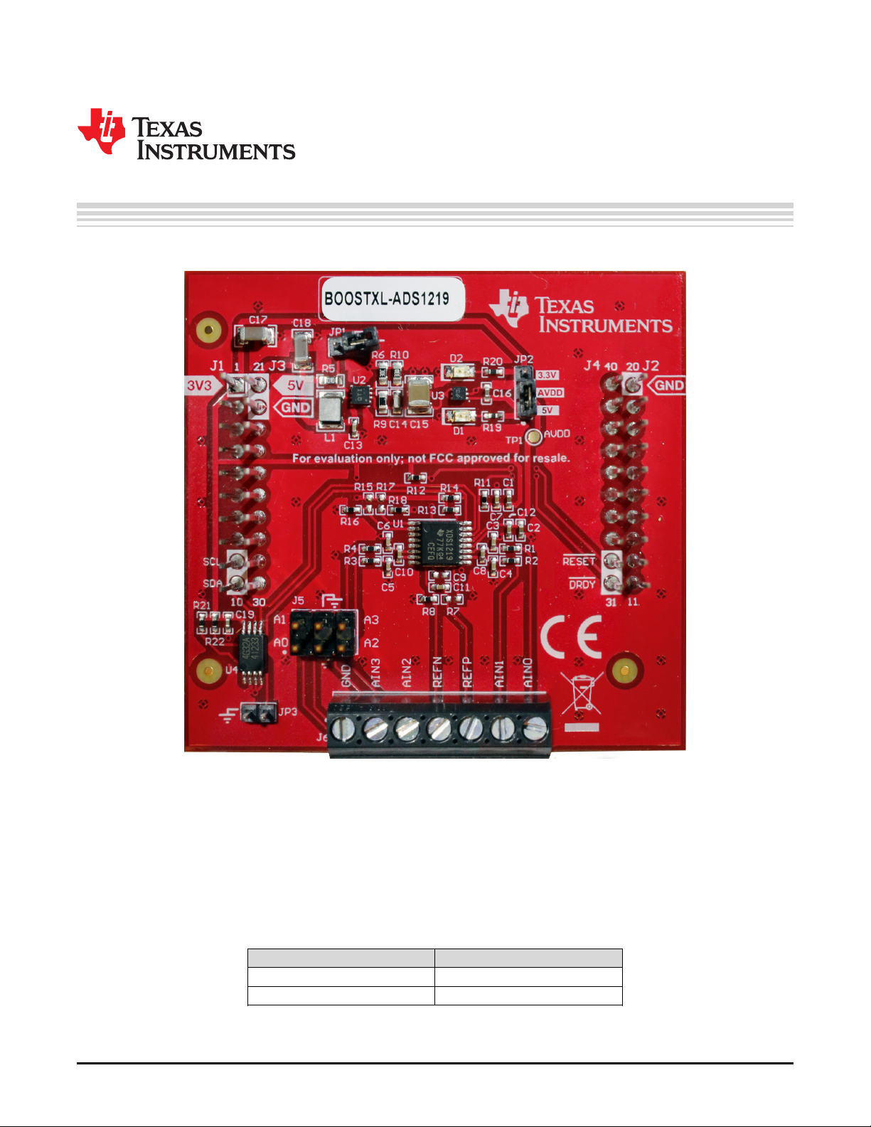
Figure 1. ADS1219 Evaluation Module (BOOSTXL-ADS1219)
The ADS1219 BoosterPack™ plug-in module (BOOSTXL-ADS1219) allows users to evaluate the
functionality of the ADS1219. The ADS1219 is a 24-bit, delta-sigma, analog-to-digital converter (ADC) that
can be configured as four single-ended inputs or as two differential input pairs. Data rates range from 20
SPS up to 1000 SPS. Processors can communicate to the ADS1219 though an I2C interface.
This user's guide includes a detailed description of the hardware (HW), bill of materials (BOM), schematic,
and software GUI when using the LaunchPad™ MSP-EXP432E401Y.
SBAU316–August 2018
Submit Documentation Feedback
Table 1. Related Documentation
Device Literature Number
ADS1219 SBAS924
MSP-EXP432E401Y SLAU748
BOOSTXL-ADS1219 BoosterPack™ User's Guide
Copyright © 2018, Texas Instruments Incorporated
1
Page 2

www.ti.com
Contents
1 Introduction ................................................................................................................... 3
2 Quick Start.................................................................................................................... 4
3 BOOSTXL-ADS1219 Hardware Overview................................................................................ 6
4 Setup Details ................................................................................................................. 8
5 ADS1219 BoosterPack™ GUI Operation ............................................................................... 12
6 Bill of Materials, PCB Layout, and Schematic.......................................................................... 16
List of Figures
1 ADS1219 Evaluation Module (BOOSTXL-ADS1219)................................................................... 1
2 Block Diagram................................................................................................................ 3
3 Quick Start.................................................................................................................... 4
4 LaunchPad™ and BoosterPack™ Combo ............................................................................... 5
5 BOOSTXL-ADS1219 Overview ............................................................................................ 6
6 Analog Supply Jumper...................................................................................................... 8
7 UniFlash: New Coniguration ............................................................................................... 9
8 UniFlash: Choose Connection ............................................................................................. 9
9 UniFlash: Browse to Firmware ........................................................................................... 10
10 UniFlash: Load Image ..................................................................................................... 10
11 UniFlash: Successful Download.......................................................................................... 11
12 Power Jumper Change.................................................................................................... 12
13 Home Page ................................................................................................................. 13
14 Quick Start Page ........................................................................................................... 13
15 Settings Page............................................................................................................... 14
16 Chart Page .................................................................................................................. 15
17 Register Map Page ........................................................................................................ 15
18 Collateral Page ............................................................................................................. 16
19 Top Silkscreen.............................................................................................................. 18
20 Top Layer ................................................................................................................... 18
21 Bottom Layer................................................................................................................ 19
22 Bottom Silkscreen.......................................................................................................... 19
23 BOOSTXL-ADS1219 Schematic ......................................................................................... 20
1 Related Documentation ..................................................................................................... 1
2 Header Input (J5) ............................................................................................................ 6
3 Terminal Block Input (J6) ................................................................................................... 6
4 MSP432E401Y Port to BoosterPack™ Interface........................................................................ 7
5 Bill of Materials ............................................................................................................. 16
Trademarks
BoosterPack, LaunchPad are trademarks of Texas Instruments.
Windows is a registered trademark of Microsoft.
2
BOOSTXL-ADS1219 BoosterPack™ User's Guide
List of Tables
Copyright © 2018, Texas Instruments Incorporated
Submit Documentation Feedback
SBAU316–August 2018
Page 3
www.ti.com
1 Introduction
The BOOSTXL-ADS1219 is a fully-assembled evaluation platform designed to highlight the ADS1219
device features and its various modes of operation.
The BOOSTXL-ADS1219 interfaces to LaunchPad™ development platforms using the XL connector
format. However, to use the ADS1219 BoosterPack™ GUI a specific LaunchPad™ (the MSPEXP432E401Y) must be used. The LaunchPad™ communicates to the ADS1219 through its I2C interface
and also acts as a USB-to-PC GUI communication bridge.
NOTE: The BOOSTXL-ADS1219 requires an external master controller to evaluate the ADS1219.
The MSP-EXP432E401Y LaunchPad™ is controlled by commands received from the ADS1219
BoosterPack™ GUI. The LaunchPad™ sends data to the GUI for display and analysis. If a LaunchPad™
is not used, the BoosterPack™ plug-in module format allows an alternate external host to communicate
with the ADS1219 using the LaunchPad™ connectors.
The BOOSTXL-ADS1219 EVM incorporates circuitry and components with the following features:
• The 24-bit ADS1219 delta-sigma ADC with four single-ended input channels (or two differential),
2.048-V reference, and I2C interface.
• External reference and analog inputs can be connected either through a header or screw terminal
block.
• 3.3-V or 5-V selectable analog power supply.
• LEDs to indicate active power supplies.
• I2C interface for the ADS1219 device configuration and communication.
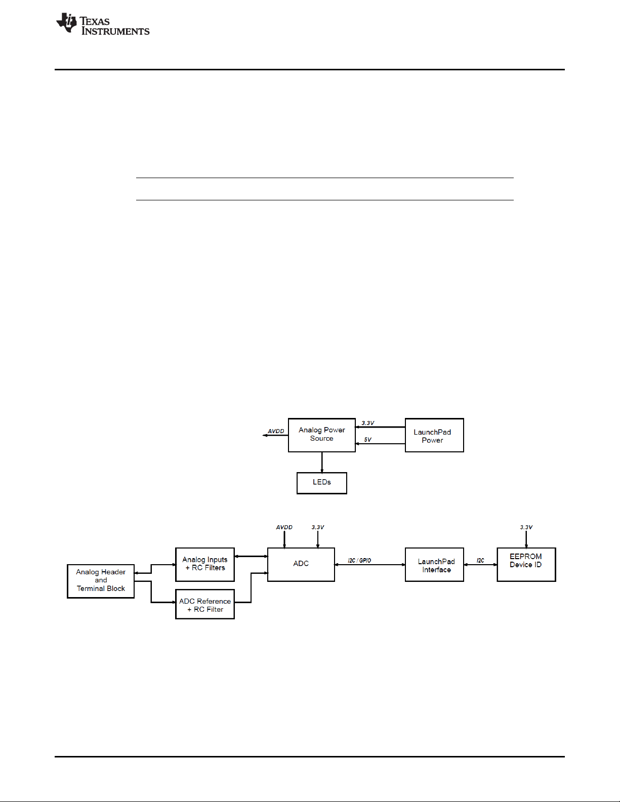
Figure 2 shows the BOOSTXL-ADS1219 EVM architecture along with key components and blocks listed in
the features.
Introduction
SBAU316–August 2018
Submit Documentation Feedback
Figure 2. Block Diagram
BOOSTXL-ADS1219 BoosterPack™ User's Guide
Copyright © 2018, Texas Instruments Incorporated
3
Page 4
Quick Start
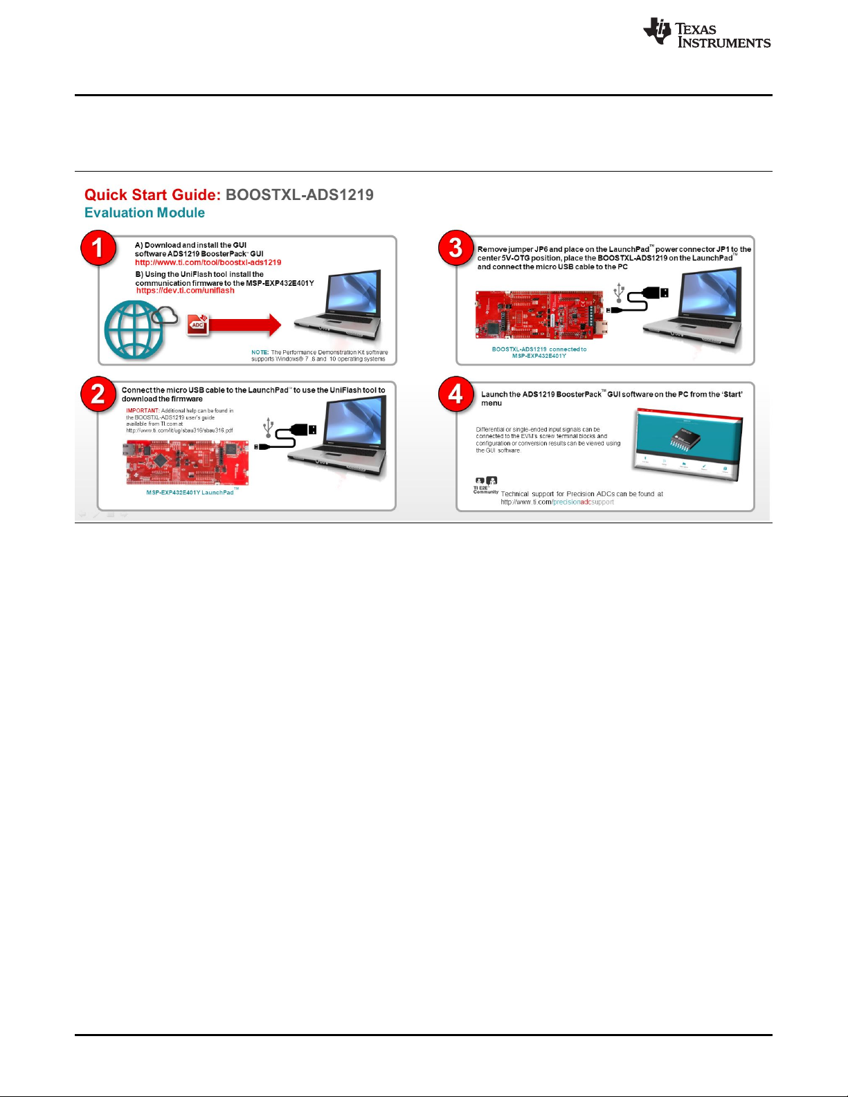
2 Quick Start
The quick start in Figure 3 shows a minimalist view of the startup procedure to get the system up and
running. Details regarding these steps can be found in Section 4.
www.ti.com
Figure 3. Quick Start
2.1 Step 1
Download and install the GUI software from the BOOSTXL-ADS1219 tools folder. This software install
also includes the firmware file required for communication with the LaunchPad™. The firmware file can be
installed to the LaunchPad™ by using the UniFlash cloud tool. A desktop version of UniFlash is also
available for download if needed.
2.2 Step 2
Connect the LaunchPad™ to the PC and download the firmware to the LaunchPad™ using the micro USB
cable provided with the LaunchPad™ kit.
2.2.1 Connect the LaunchPad™
Connect the USB cable from the PC to the micro USB connector on the top portion of the LaunchPad™
(XDS110 portion of the LaunchPad™). A green LED lights up indicating that the LaunchPad™ is powered.
2.2.2 Start the UniFlash Program and Choose the Correct LaunchPad™
Start the UniFlash program and begin a New Configuration (Figure 7) and select the LaunchPad™ MSPEXP432E401Y.
The connection type is automatically chosen based on the LaunchPad™ being used. Verify that the Texas
Instruments XDS110 USB Debug Probe is selected and press Start.
2.2.3 Choose the Firmware File and Flash the LaunchPad™
The firmware file is located in the folder Program Files (x86)\Texas Instruments\ADS1219\firmware. Use
the Browse button to browse to folder containing the firmware binary file. The firmware file can also be
dragged and dropped into the browse window provided in UniFlash.
4
BOOSTXL-ADS1219 BoosterPack™ User's Guide
Copyright © 2018, Texas Instruments Incorporated
Submit Documentation Feedback
SBAU316–August 2018
Page 5
www.ti.com
When the desired firmware is selected, use the Load Image button to load the firmware into the
LaunchPad™.
Verify that the firmware installed successfully by checking the Console portion of the UniFlash tool at the
bottom of the GUI window.
2.3 Step 3
After the firmware file has successfully downloaded to the LaunchPad™, unplug the USB cable from the
LaunchPad™. Further communication takes place using the USB connector located at the opposite end of
the LaunchPad™. For proper power to be supplied to the BOOSTXL-ADS1219, remove the jumper from
the middle of the LaunchPad™ at JP6 and place the jumper on the center pins of JP1 (see Figure 12).
This jumper takes the available USB power from the bottom connector and applies the voltage to the
remainder of the board.
Before plugging the USB cable to the bottom LaunchPad™ USB connector, properly align the connectors
and attach the BOOSTXL-ADS1219 BoosterPack™ to the bottom set of connectors on the LaunchPad™
(Figure 4).
Quick Start
When the BoosterPack™ is attached, plug the USB cable into the bottom connector of the LaunchPad™
and also to the PC. The LaunchPad™ communication to the PC is USB communications device class
(CDC) using a virtual COM port. Windows®10 automatically installs the required driver. Earlier versions of
the operating system may require a manual driver installation. The required driver files can be found in the
installation directory Program Files (x86)/Texas Instruments/ADS1219/drivers.
2.4 Step 4
From the Windows Start menu, go to the Texas Instruments folder and under ADS1219 start the GUI
application. The communication should automatically connect. If the hardware does not connect, manually
try to make the connection by clicking on the connect icon in the lower left portion of the GUI.
SBAU316–August 2018
Submit Documentation Feedback
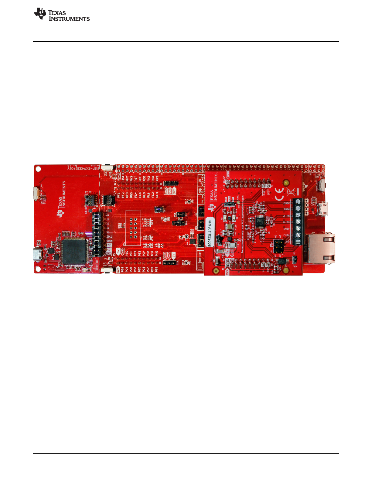
Figure 4. LaunchPad™ and BoosterPack™ Combo
BOOSTXL-ADS1219 BoosterPack™ User's Guide
Copyright © 2018, Texas Instruments Incorporated
5
Page 6
BOOSTXL-ADS1219 Hardware Overview
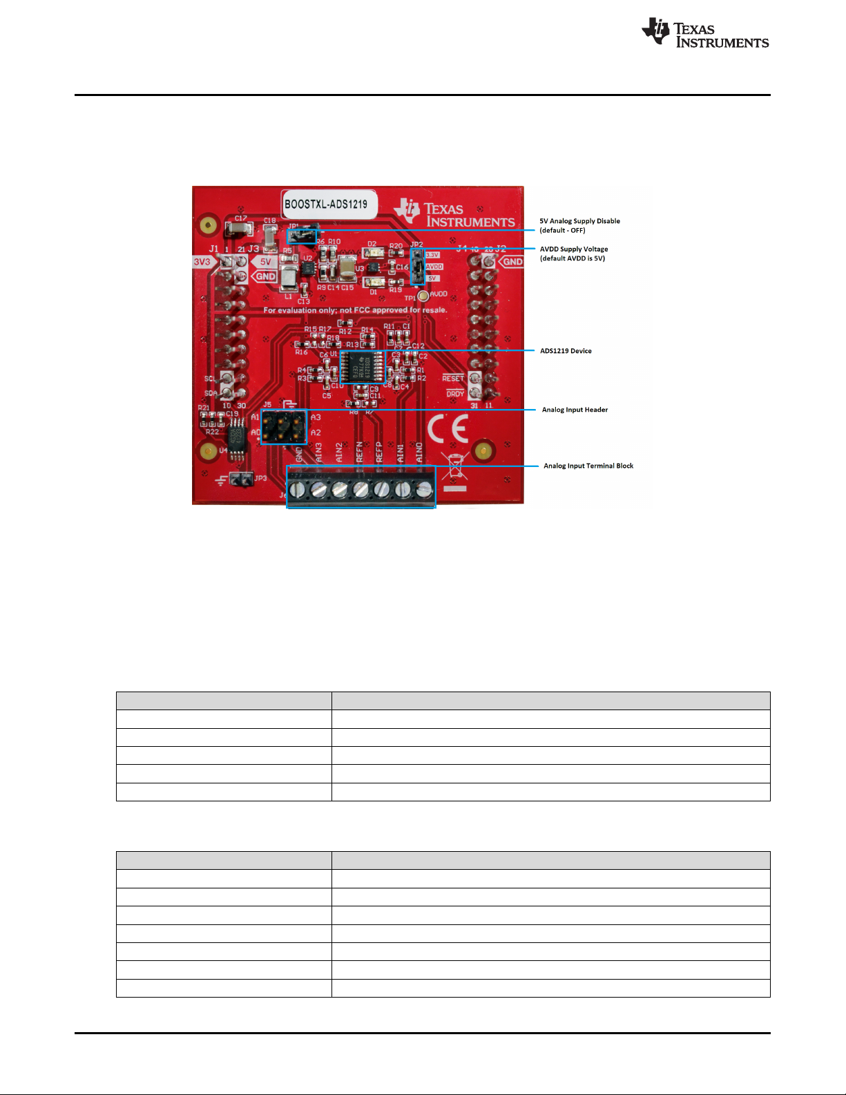
3 BOOSTXL-ADS1219 Hardware Overview
This section lists various onboard components that are used to interface analog inputs, analog reference,
digital interface, and power to the BOOSTXL-ADS1219 EVM. Figure 5 shows a top-level view of the
board.
www.ti.com
Figure 5. BOOSTXL-ADS1219 Overview
3.1 Connectors for the Analog Input
The BOOSTXL-ADS1219 EVM is designed for easy interface to analog sources through a 100-mil header
(J5) or to a screw terminal block (J6). J6 also allows for an external reference input. Table 2 shows the
input configuration for J5 and Table 3 shows the configuration for J6. Both connectors are clearly labeled
on the PCB silkscreen for easy input connection identification.
J5 Connector Pin Description
J5:1 Analog input for A0 of the ADC
J5:2 Analog input for A1 of the ADC
J5:3 and J5:4 BoosterPack™ plug-in module ground
J5:5 Analog input for A2 of the ADC
J5:6 Analog input for A3 of the ADC
Table 3. Terminal Block Input (J6)
J6 Terminal Block Inputs Description
J6:1 BoosterPack™ plug-in module ground
J6:2 Analog input for A3 of the ADC
J6:3 Analog input for A2 of the ADC
J6:4 Analog reference input REFN
J6:5 Analog reference input REFP
J6:6 Analog input for A1 of the ADC
J6:7 Analog input for A0 of the ADC
Table 2. Header Input (J5)
6
BOOSTXL-ADS1219 BoosterPack™ User's Guide
Copyright © 2018, Texas Instruments Incorporated
Submit Documentation Feedback
SBAU316–August 2018
Page 7

www.ti.com
The analog inputs can range from GND up to AVDD, which is the analog supply voltage. A maximum of
four single-ended inputs, or two differential inputs may be applied to the ADS1219. The user can configure
the input channels through the ADS1219 BoosterPack™ GUI. Each of the analog inputs have a series 1kΩ resistor with a 100-nF differential capacitor between inputs and a 10-nF common-mode capacitor to
GND for filtering noise and aliasing. Figure 23 provides a schematic that details the input filtering.
3.2 Voltage Reference
The ADS1219 contains an internal 2.048-V reference and no external reference is required. The analog
supply can also be used as reference input by installing a 0-Ω resistor at R7. An external reference can be
applied to the terminal block REFP and REFN connections available on J6 (see the analog input terminal
block in Figure 5). The external reference input is limited by a minimum of 0.75 V and a maximum of the
analog supply voltage (AVDD). The REFN input is connected to the board ground by default through the
0-Ω resistor R8.
3.3 Digital Interface
The BOOSTXL-ADS1219 interfaces to the MSP-EXP432E401Y LaunchPad™, which in turn
communicates with the computer through USB. The two devices are on the BoosterPack™ and they both
communicate using I2C. U4 is an EEPROM used to hold device and board manufacturing information. The
EEPROM information is not currently available to the GUI. U1 is the ADS1219 and communication from
the GUI allows for register read and write as well as ADC conversion data collection.
3.4 BOOSTXL-ADS1219 Digial I/O
The BOOSTXL-ADS1219 EVM supports the I2C digital interface and functional modes as described in the
ADS1219 datasheet. The LaunchPad™ operates at a 3.3-V logic and I/O level. The ADS1219 has both
DVDD and AVDD. DVDD is the digital supply and is fixed to the same voltage level as the LaunchPad™
processor so no level shifting is required. The I2C communication is through LaunchPad™ ports PN5
(SCL) and PN4 (SDA). GPIO pin control for the Reset pin of the ADS1219 is controlled by port PK6. The
Reset control pin defaults high (not in reset). GPIO port PK7 is an input port pin used to interrupt the
processor when a new conversion result is ready to be read from the ADS1219. Table 4 lists the port to
connector pin interface.
BOOSTXL-ADS1219 Hardware Overview
Table 4. MSP432E401Y Port to BoosterPack™ Interface
MSP-EXP432E401Y GPIO Port
SCL (PN5 - Output) J1:9
SDA (PN4 - Input/Output) J1:10
RESET (PK6 - Output) J4:32
DRDY (PK7 - Input) J4:31
BOOSTXL-ADS1219 Connector
Pin
SBAU316–August 2018
Submit Documentation Feedback
BOOSTXL-ADS1219 BoosterPack™ User's Guide
Copyright © 2018, Texas Instruments Incorporated
7
Page 8
BOOSTXL-ADS1219 Hardware Overview
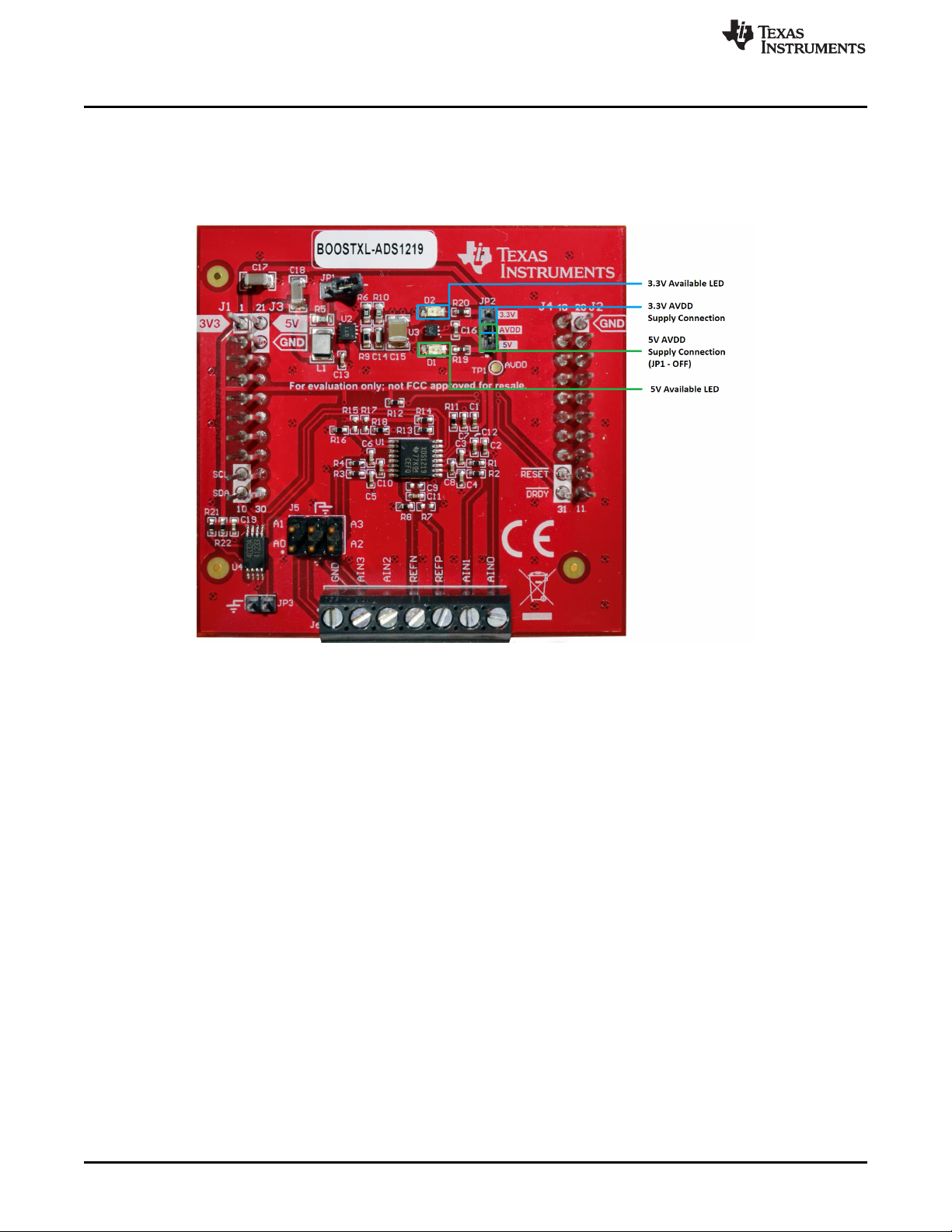
3.5 Power Supply
Both the LaunchPad™ 3.3-V and 5-V supplies are used for the BOOSTXL-ADS1219. The digital supply is
3.3 V and supplies the ADS1219 DVDD supply input. AVDD is the ADS1219 analog supply and can
accommodate either 3.3-V or 5-V operation. The choice of analog supply voltage is selected by jumper
JP2. JP2:1-2 selects the 5-V supply source and JP2:2-3 selects the 3.3-V source, as shown in Figure 6.
www.ti.com
Figure 6. Analog Supply Jumper
The 3.3-V source comes directly from the LaunchPad™ and when available on the BOOSTXL-ADS1219
the D2 LED lights up indicating that the supply is active. The LaunchPad™ 5-V source is often less than
5 V. To achieve a stable voltage when operating at 5-V AVDD, U3 is used to charge pump the
LaunchPad™ 5-V source and regulate for a fixed 5-V output. U3 can be disabled by installing jumper JP1,
but by default this jumper is not installed. When U3 is active, then LED D1 lights up indicating the supply
is available. TP1 can be used to monitor the AVDD supply voltage. Jumper placement and LEDs are
shown in Figure 6.
4 Setup Details
Getting the BOOSTXL-ADS1219 and MSP-EXP432E401Y LaunchPad™ combination to communicate
with the PC requires firmware to be installed in the LaunchPad™ (see Section 4.2.1). This firmware is
made available as part of the ADS1219 BoosterPack™ GUI software installation. Depending on which
operating system is being used, there may also be a need for driver installation. The drivers are also
included as a part of the GUI software installation.
4.1 ADS1219 BoosterPack™ GUI Installation
Download and install the GUI from the BOOSTXL-ADS1219 tools folder. The license agreements must be
accepted or the software will not install. Follow all remaining on-screen instructions to complete the
installation.
4.2 Using the UniFlash Tool to Program the LaunchPad™
The UniFlash program can be accessed via the cloud or by download. When using the cloud version for
the first time the TI cloud agent must be installed. Follow all instructions by downloading and installing the
correct cloud version for the operating system being used.
8
BOOSTXL-ADS1219 BoosterPack™ User's Guide
Copyright © 2018, Texas Instruments Incorporated
Submit Documentation Feedback
SBAU316–August 2018
Page 9

www.ti.com
4.2.1 Flashing the Firmware
When the UniFlash program is accessed, either by cloud or download, start the process by first plugging
in the LaunchPad™ to the XDS110 programming connector at the top of the LaunchPad™. A green LED
lights up indicating that power is available and the cloud agent driver recognizes and installs the
appropriate drivers for the LaunchPad™. For any issues with the installation or operation of the UniFlash
program, click on the Help icon in the UniFlash menu bar.
1. In the UniFlash program start a New Configuration by selecting the MSP-EXP432E401Y LaunchPad™
from the drop down list as shown in Figure 7.
Setup Details
Figure 7. UniFlash: New Coniguration
2. The Selected Connection happens automatically to Texas Instruments XDS110 USB Debug Probe as
seen in Figure 8, then press Start.
Figure 8. UniFlash: Choose Connection
SBAU316–August 2018
Submit Documentation Feedback
BOOSTXL-ADS1219 BoosterPack™ User's Guide
Copyright © 2018, Texas Instruments Incorporated
9
Page 10

Setup Details
3. From the Program tab, Browse to the Flash Image to be installed, as shown in Figure 9. The flash
binary file is found under the Program Files (x86)\Texas Instruments\ADS1219\fimware folder.
www.ti.com
Figure 9. UniFlash: Browse to Firmware
4. When the flash binary image file is located, press the Load Image button to start the firmware
download, as shown in Figure 10.
10
Figure 10. UniFlash: Load Image
BOOSTXL-ADS1219 BoosterPack™ User's Guide
Copyright © 2018, Texas Instruments Incorporated
Submit Documentation Feedback
SBAU316–August 2018
Page 11

www.ti.com
5. The console at the bottom of the UniFlash window shows the result of the loading process. The correct
Setup Details
response is [SUCCESS] Program Load completed successfully, as shown in Figure 11. If this
response is not shown or an error message is displayed try the Load Image button again. You may
have to unplug and plug the USB cable to the LaunchPad™ again to reset communication.
Figure 11. UniFlash: Successful Download
SBAU316–August 2018
Submit Documentation Feedback
BOOSTXL-ADS1219 BoosterPack™ User's Guide
Copyright © 2018, Texas Instruments Incorporated
11
Page 12

Setup Details
4.2.2 LaunchPad™ Power Configuration
To reduce the number of cables required to communicate and power the BOOSTXL-ADS1219, the USB
connection at U7 can be used as the supply source for the LaunchPad™ as well as the communication
connection for the CDC virtual COM port to the GUI. To route the power correctly, use the jumper installed
on JP6 and connect to JP1 at the 5V-OTG (center) position as shown in Figure 12. There should now be
two jumpers on JP1.
www.ti.com
Figure 12. Power Jumper Change
4.3 Driver Installation (If Required)
For Windows 10, the enumeration of a CDC device automatically installs the required driver on
enumeration. For earlier versions of the operating system a communication device class driver (CDC) may
need to be installed. If the driver shows as unknown, manually install the driver from Program Files
(x86)/Texas Instruments/ADS1219/drivers. Go to the Control Panel and select Device Manager. Right click
on the unknown device and select Update driver. Choose the selection Browse my computer for driver
software. Browse to the driver folder location and choose Next to locate the correct driver.
5 ADS1219 BoosterPack™ GUI Operation
Figure 13 illustrates the home page of the ADS1219 BoosterPack™ GUI. This page provides a high-level
overview of the ADS1219 device. Starting at the upper left portion of the GUI are various icons that refer
to particular pages within the GUI application. Along with the home page is the quick start, setup, chart,
register, and collateral pages. Each page can be selected by clicking on the appropriate icon. When the
MSP-EXP432E401Y LaunchPad™ is combined with the BOOSTXL-ADS1219 BoosterPack™ and
connected to the PC with the micro USB cable, the board is detected and connected. The connection
status is shown at the lower left corner of the GUI.
12
BOOSTXL-ADS1219 BoosterPack™ User's Guide
Copyright © 2018, Texas Instruments Incorporated
Submit Documentation Feedback
SBAU316–August 2018
Page 13

www.ti.com
5.1 Home Page
The Home page is the starting point of the GUI application. The five other pages can be selected from the
bottom portion of the page, or from the icons along the left-hand side of the window. By clicking on Learn
more, the ADS1219 features and functional diagram will be displayed in place of the page control tabs.
When clicking on Show Less the page control tabs are once again displayed.
ADS1219 BoosterPack™ GUI Operation
5.2 Quick Start Page
The Quick Start page (Figure 14) shows a minimal view of the startup procedure to get the system up and
running. For specific details see Section 4.
Figure 13. Home Page
SBAU316–August 2018
Submit Documentation Feedback
Figure 14. Quick Start Page
BOOSTXL-ADS1219 BoosterPack™ User's Guide
Copyright © 2018, Texas Instruments Incorporated
13
Page 14

ADS1219 BoosterPack™ GUI Operation
5.3 Settings Page
There is only one control setting on the Settings page (Figure 15). The control can be used to force a
hardware reset to the ADS1219. Clicking the Reset button twice forces the reset pin low with the first click,
and then returns the pin high with the second button click.
www.ti.com
5.4 Chart Page
There is only one Chart page option available (Figure 16) and that is the Time Domain Analysis plot. For
any data to be displayed in a continuous mode of operation requires that the Conversion Mode in the
ADS1219 register setting be set to Continuous.
5.4.1 Time Domain Analysis
The plot begins when the START button in pressed. When the chart begins to display data, the START
button changes to STOP. Data are displayed on the chart until the STOP button is pressed. There are two
ways the data can be displayed. One option is to display by voltage and the second option displays by the
number of codes. The voltage option is the default, and the voltage value displayed depends on the gain
applied in the register setting and the reference voltage being used. The default reference voltage
displayed is the internal reference voltage of the ADS1219. If another reference source is used, update
the reference voltage box to accurately display the voltage value determined at the ADC input.
Figure 15. Settings Page
14
BOOSTXL-ADS1219 BoosterPack™ User's Guide
Copyright © 2018, Texas Instruments Incorporated
Submit Documentation Feedback
SBAU316–August 2018
Page 15

www.ti.com
5.5 Register Map Page
The Register Map page (Figure 17) displays the contents of the ADS1219 registers. Only the first register
can be written. The second register is a read-only register. Register settings can be changed using the
drop-down lists and click boxes. Information regarding the selections and options can be displayed by
using the cursor to hover over the various options.
ADS1219 BoosterPack™ GUI Operation
Figure 16. Chart Page
SBAU316–August 2018
Submit Documentation Feedback
Figure 17. Register Map Page
BOOSTXL-ADS1219 BoosterPack™ User's Guide
Copyright © 2018, Texas Instruments Incorporated
15
Page 16

ADS1219 BoosterPack™ GUI Operation
5.6 Collateral Page
The Collateral page (Figure 18) provides information and links to various application notes and any other
useful information as applicable to the GUI or the BOOSTXL-ADS1219.
www.ti.com
Figure 18. Collateral Page
6 Bill of Materials, PCB Layout, and Schematic
This section contains the BOOSTXL-ADS1219 EVM bill of materials (BOM), printed-circuit board (PCB)
layout, and board schematic.
6.1 Bill of Materials
Table 5 lists the bill of materials (BOM) for the BOOSTXL-ADS1219 EVM.
Table 5. Bill of Materials
Designator Quantity Description Manufacturer Part
!PCB1 1 Printed Circuit Board DC023 Any
C1, C2, C16 3 CAP, CERM, 1 uF, 10 V, +/- 10%,
C3, C4, C5, C6 4 CAP, CERM, 0.01 uF, 10 V, +/- 10%,
C7, C8, C10,
C11, C12, C13,
C19
C14 1 CAP, CERM, 100 pF, 25 V, +/- 10%,
C15 1 CAP, CERM, 22 uF, 25 V, +/- 20%,
C17, C18 2 CAP, CERM, 10 uF, 16 V, +/- 10%,
7 CAP, CERM, 0.1 uF, 10 V, +/- 10%,
X7S, 0402
X7R, 0402
X7R, 0402
X7R, 0603
X7R, 1210
X5R, 1206
Number
Manufacturer
C1005X7S1A105K050BC TDK
0402ZC103KAT2A AVX
GRM155R71A104KA01D MuRata
06033C101KAT2A AVX
TMK325B7226MM-TR Taiyo Yuden
GRM319R61C106KE15D MuRata
16
BOOSTXL-ADS1219 BoosterPack™ User's Guide
Submit Documentation Feedback
SBAU316–August 2018
Copyright © 2018, Texas Instruments Incorporated
Page 17

www.ti.com
Bill of Materials, PCB Layout, and Schematic
Table 5. Bill of Materials (continued)
D1, D2 2 LED, Green, SMD LTST-C171GKT Lite-On
J1/J3, J2/J4 2 Receptacle, 2.54mm, 10x2, Tin, TH SSQ-110-03-T-D Samtec
J5 1 Header, 100mil, 3x2, Gold, TH TSW-103-07-G-D Samtec
J6 1 Terminal Block, 3.5mm Pitch, 7x1, TH ED555/7DS On-Shore Technology
JP1, JP3 2 Header, 2mm, 2x1, Tin, TH TMM-102-01-T-S Samtec
JP2 1 Header, 2mm, 3x1, Tin, TH TMM-103-01-T-S Samtec
L1 1 Inductor, Wirewound, Ferrite, 1 uH,
R1, R2, R3, R4,
R13, R14
R5 1 RES, 100 k, 1%, 0.1 W, AEC-Q200
R6 1 RES, 20.0 k, 1%, 0.1 W, 0603 RC0603FR-0720KL Yageo
R8 1 RES, 0, 5%, 0.1 W, AEC-Q200 Grade
R9 1 RES, 768 k, 1%, 0.1 W, 0603 RC0603FR-07768KL Yageo
R10 1 RES, 215 k, 1%, 0.1 W, 0603 RC0603FR-07215KL Yageo
R11, R12, R16,
R18, R21, R22
R19 1 RES, 160, 5%, 0.063 W, AEC-Q200
R20 1 RES, 100, 1%, 0.063 W, AEC-Q200
SH-JP1, SH-JP2 2 Shunt, 2mm, Gold plated, Black 2SN-BK-G Samtec
U1 1 24-Bit, 4-Channel, 1-kSPS, Delta-
U2 1 3.5MHz, 1.5A, 92% Efficient Boost
U3 1 Single Output High PSRR LDO, 150
U4 1 I2C BUS EEPROM (2-Wire), TSSOP-B8BR24G32FVT-3AGE2 Rohm
6 RES, 1.00 k, 1%, 0.063 W, AEC-Q200
6 RES, 10 k, 5%, 0.1 W, AEC-Q200
2.05 A, 0.045 ohm, SMD
Grade 0, 0402
Grade 0, 0603
0, 0402
Grade 0, 0402
Grade 0, 0402
Grade 0, 0402
Sigma ADC with I2C Interface,
PW0016A (TSSOP-16)
Converter with Adjustable Input
Current Limit, DSG0008A (WSON-8)
mA, Fixed 5 V Output, 2.5 to 6.5 V
Input, with Low IQ, 6-pin WSON
(DSE), -40 to 125 degC, Green (RoHS
& no Sb/Br)
LQH32PN1R0NN0 MuRata
CRCW04021K00FKED Vishay-Dale
CRCW0603100KFKEA Vishay-Dale
ERJ-2GE0R00X Panasonic
ERJ-2GEJ103X Panasonic
CRCW0402160RJNED Vishay-Dale
CRCW0402100RFKED Vishay-Dale
ADS1219IPWR Texas Instruments
TPS61252DSGR Texas Instruments
TPS71750DSER Texas Instruments
C9 0 CAP, CERM, 0.1 uF, 10 V, +/- 10%,
R7 0 RES, 0, 5%, 0.1 W, AEC-Q200 Grade
R15, R17 0 RES, 10 k, 5%, 0.1 W, AEC-Q200
SH-JP3 0 Shunt, 2mm, Gold plated, Black 2SN-BK-G Samtec
SBAU316–August 2018
Submit Documentation Feedback
X7R, 0402
0, 0402
Grade 0, 0402
Copyright © 2018, Texas Instruments Incorporated
GRM155R71A104KA01D MuRata
ERJ-2GE0R00X Panasonic
ERJ-2GEJ103X Panasonic
BOOSTXL-ADS1219 BoosterPack™ User's Guide
17
Page 18

Bill of Materials, PCB Layout, and Schematic
6.2 PCB Layout
Figure 19 to Figure 22 depict the BOOSTXL-ADS1219EVM PCB layout.
www.ti.com
Figure 19. Top Silkscreen
Figure 20. Top Layer
18
BOOSTXL-ADS1219 BoosterPack™ User's Guide
Copyright © 2018, Texas Instruments Incorporated
Submit Documentation Feedback
SBAU316–August 2018
Page 19

www.ti.com
Bill of Materials, PCB Layout, and Schematic
Figure 21. Bottom Layer
SBAU316–August 2018
Submit Documentation Feedback
Figure 22. Bottom Silkscreen
BOOSTXL-ADS1219 BoosterPack™ User's Guide
Copyright © 2018, Texas Instruments Incorporated
19
Page 20

1
1
2
2
3
3
4
4
5
5
6
6
D D
C C
B B
A A
2 3
ADC and Power Supply
7/3/2018
DC023_Schematic.SchDoc
SheetTitle:
Size:
Mod. Date:
File:
Sheet: of
B http://www.ti.com
Contact: http://www.ti.com/support
BOOSTXL-ADS1x19ProjectTitle:
Designedfor: Public Release
Assembly Variant: 001
Drawn By:
Engineer:
Benjamin/Mendez
RobertBenjamin
TexasInstruments and/or its licensorsdo not warrant the accuracyor completeness of thisspecification or any informationcontained therein.Texas Instrumentsand/or its licensors do not
warrant that this design willmeet the specifications, willbe suitable foryour application or fit for any particular purpose,or will operate in animplementation. TexasInstruments and/or its
licensorsdo not warrantthat the design is production worthy. Youshould completelyvalidate and testyour design implementationto confirm the systemfunctionality for yourapplication.
Version controldisabledSVN Rev:
DC023Number: Rev: A
TID #: N/A
Orderable: BOOSTXL-ADS1219
Launchpad Connectors
LP5V
215k
R10
768k
R9
22uF
C15
100pF
C14
243k= 5V
215k= 5.5V
191k= 6V
Power Supply Generation Circuit
AVDD
GND
GND
1
VOUT
2
FB
3
ILIM
4
PG
5
EN
6
SW
7
VIN
8
PAD
9
U2
TPS61252
L1
20.0k
R6
100k
R5
GND
Green
D1
GND
GND
GNDGNDGND
SCL
SDA
GND GND
LP3.3V LP3.3V
GND
AVDD
A0
A1
A0A1
GND
AIN0
AIN1
AIN2
AIN3
LP3.3V
DRDY
LP3.3V
GND
0.1uF
C7
LP3.3V
RESET
DRDY
RESET
SCL
SDA
GND
GND
GND
GND
GND
AVDD
1uF
C1
GND
1uF
C2
GND
LP3.3V
LP3.3V
SCL
REFP
REFN
REFP
REFN
SDA
GND
OUT
1
NR3EN
4
NC
5
IN
6
2
GND
TPS71750DSERU3
1uF
C16
GND
GND
LP3.3V
100
R20
160
R19
5V
GPIO !
31
GPIO !
32
GPIO !
33
GPIO !
34
Timer_Cap/GPIO !
35
Timer_Cap/GPIO !
36
PWM/GPIO !
37
PWM/GPIO !
38
PWM/GPIO !
39
PWM/GPIO !
40
GPIO !
11
SPI_CS/GPIO !
12
SPI_CS/GPIO !
13
SPI_MISO
14
SPI_MOSI
15
RST
16
GPIO
17
GPIO !
18
PWM/GPIO !
19
GND
20
J2/J4
SSQ-110-03-T-D
+3.3V
1
Analog_In
2
LP_UART_RX
3
LP_UART_TX
4
GPIO !
5
Analog In
6
SPI_CLK
7
GPIO !
8
I2C_SCL
9
I2C_SDA
10
+5V
21
GND
22
Analog_In
23
Analog_In
24
Analog_In
25
Analog_In
26
Analog_In/I2S_WS
27
Analog_In/I2S_SCLK
28
Analog_Out/I2S_SDout
29
Analog_Out/I2S_SDin
30
J1/J3
SSQ-110-03-T-D
GND
RESET
LP5V
GND
GND
DRDY
LP3.3V
GND
A0
1
A1
2
A2
3
VSS4SDA
5
SCL
6
WP
7
VCC
8
U4
BR24G32FVT-3AGE2
LP3.3V
GND
SCL
SDA
GND
GND
1
2
3
JP2
JP3
JP1
0.1uF
C12
0.1uF
C11
0.1uF
C13
0.1uF
C19
10k
R21
10k
R22
10k
R12
10k
R16
10k
R18
10k
R17
DNP
10k
R15
DNP
10k
R11
ADC
EEPROM Memory
1 2
3 4
5 6
J5
GND
Green
D2
AIN0
11
AIN1
10
AIN2
7
AIN3
6
AVDD
12
AGND
5
DGND
4
DVDD
13
A1
2
A0
1
DRDY
14
REFN
8
REFP
9
SCL
16
SDA
15
RESET
3
ADS1219IPWR
U1
GND
5
4
1
2
3
6
7
J6
ED555/7DS
1.00k
R1
1.00k
R4
1.00k
R2
1.00k
R3
0.01uF
C3
0.01uF
C6
0.01uF
C4
0.01uF
C5
0.1uF
C8
0.1uF
C10
0.1uF
C9
DNP
AIN0 AIN1
AIN2 AIN3
TP1
AVDD
1.00k
R13
1.00k
R14
0
R7
DNP
0
R8
10uF
C17
10uF
C18
Bill of Materials, PCB Layout, and Schematic
6.3 Schematic
Figure 23 shows the BOOSTXL-ADS1219 schematic.
www.ti.com
Figure 23. BOOSTXL-ADS1219 Schematic
20
BOOSTXL-ADS1219 BoosterPack™ User's Guide
Copyright © 2018, Texas Instruments Incorporated
Submit Documentation Feedback
SBAU316–August 2018
Page 21

STANDARD TERMS FOR EVALUATION MODULES
1. Delivery: TI delivers TI evaluation boards, kits, or modules, including any accompanying demonstration software, components, and/or
documentation which may be provided together or separately (collectively, an “EVM” or “EVMs”) to the User (“User”) in accordance
with the terms set forth herein. User's acceptance of the EVM is expressly subject to the following terms.
1.1 EVMs are intended solely for product or software developers for use in a research and development setting to facilitate feasibility
evaluation, experimentation, or scientific analysis of TI semiconductors products. EVMs have no direct function and are not
finished products. EVMs shall not be directly or indirectly assembled as a part or subassembly in any finished product. For
clarification, any software or software tools provided with the EVM (“Software”) shall not be subject to the terms and conditions
set forth herein but rather shall be subject to the applicable terms that accompany such Software
1.2 EVMs are not intended for consumer or household use. EVMs may not be sold, sublicensed, leased, rented, loaned, assigned,
or otherwise distributed for commercial purposes by Users, in whole or in part, or used in any finished product or production
system.
2 Limited Warranty and Related Remedies/Disclaimers:
2.1 These terms do not apply to Software. The warranty, if any, for Software is covered in the applicable Software License
Agreement.
2.2 TI warrants that the TI EVM will conform to TI's published specifications for ninety (90) days after the date TI delivers such EVM
to User. Notwithstanding the foregoing, TI shall not be liable for a nonconforming EVM if (a) the nonconformity was caused by
neglect, misuse or mistreatment by an entity other than TI, including improper installation or testing, or for any EVMs that have
been altered or modified in any way by an entity other than TI, (b) the nonconformity resulted from User's design, specifications
or instructions for such EVMs or improper system design, or (c) User has not paid on time. Testing and other quality control
techniques are used to the extent TI deems necessary. TI does not test all parameters of each EVM.
User's claims against TI under this Section 2 are void if User fails to notify TI of any apparent defects in the EVMs within ten (10)
business days after delivery, or of any hidden defects with ten (10) business days after the defect has been detected.
2.3 TI's sole liability shall be at its option to repair or replace EVMs that fail to conform to the warranty set forth above, or credit
User's account for such EVM. TI's liability under this warranty shall be limited to EVMs that are returned during the warranty
period to the address designated by TI and that are determined by TI not to conform to such warranty. If TI elects to repair or
replace such EVM, TI shall have a reasonable time to repair such EVM or provide replacements. Repaired EVMs shall be
warranted for the remainder of the original warranty period. Replaced EVMs shall be warranted for a new full ninety (90) day
warranty period.
3 Regulatory Notices:
3.1 United States
3.1.1 Notice applicable to EVMs not FCC-Approved:
FCC NOTICE: This kit is designed to allow product developers to evaluate electronic components, circuitry, or software
associated with the kit to determine whether to incorporate such items in a finished product and software developers to write
software applications for use with the end product. This kit is not a finished product and when assembled may not be resold or
otherwise marketed unless all required FCC equipment authorizations are first obtained. Operation is subject to the condition
that this product not cause harmful interference to licensed radio stations and that this product accept harmful interference.
Unless the assembled kit is designed to operate under part 15, part 18 or part 95 of this chapter, the operator of the kit must
operate under the authority of an FCC license holder or must secure an experimental authorization under part 5 of this chapter.
3.1.2 For EVMs annotated as FCC – FEDERAL COMMUNICATIONS COMMISSION Part 15 Compliant:
CAUTION
This device complies with part 15 of the FCC Rules. Operation is subject to the following two conditions: (1) This device may not
cause harmful interference, and (2) this device must accept any interference received, including interference that may cause
undesired operation.
Changes or modifications not expressly approved by the party responsible for compliance could void the user's authority to
operate the equipment.
FCC Interference Statement for Class A EVM devices
NOTE: This equipment has been tested and found to comply with the limits for a Class A digital device, pursuant to part 15 of
the FCC Rules. These limits are designed to provide reasonable protection against harmful interference when the equipment is
operated in a commercial environment. This equipment generates, uses, and can radiate radio frequency energy and, if not
installed and used in accordance with the instruction manual, may cause harmful interference to radio communications.
Operation of this equipment in a residential area is likely to cause harmful interference in which case the user will be required to
correct the interference at his own expense.
Page 22

FCC Interference Statement for Class B EVM devices
NOTE: This equipment has been tested and found to comply with the limits for a Class B digital device, pursuant to part 15 of
the FCC Rules. These limits are designed to provide reasonable protection against harmful interference in a residential
installation. This equipment generates, uses and can radiate radio frequency energy and, if not installed and used in accordance
with the instructions, may cause harmful interference to radio communications. However, there is no guarantee that interference
will not occur in a particular installation. If this equipment does cause harmful interference to radio or television reception, which
can be determined by turning the equipment off and on, the user is encouraged to try to correct the interference by one or more
of the following measures:
• Reorient or relocate the receiving antenna.
• Increase the separation between the equipment and receiver.
• Connect the equipment into an outlet on a circuit different from that to which the receiver is connected.
• Consult the dealer or an experienced radio/TV technician for help.
3.2 Canada
3.2.1 For EVMs issued with an Industry Canada Certificate of Conformance to RSS-210 or RSS-247
Concerning EVMs Including Radio Transmitters:
This device complies with Industry Canada license-exempt RSSs. Operation is subject to the following two conditions:
(1) this device may not cause interference, and (2) this device must accept any interference, including interference that may
cause undesired operation of the device.
Concernant les EVMs avec appareils radio:
Le présent appareil est conforme aux CNR d'Industrie Canada applicables aux appareils radio exempts de licence. L'exploitation
est autorisée aux deux conditions suivantes: (1) l'appareil ne doit pas produire de brouillage, et (2) l'utilisateur de l'appareil doit
accepter tout brouillage radioélectrique subi, même si le brouillage est susceptible d'en compromettre le fonctionnement.
Concerning EVMs Including Detachable Antennas:
Under Industry Canada regulations, this radio transmitter may only operate using an antenna of a type and maximum (or lesser)
gain approved for the transmitter by Industry Canada. To reduce potential radio interference to other users, the antenna type
and its gain should be so chosen that the equivalent isotropically radiated power (e.i.r.p.) is not more than that necessary for
successful communication. This radio transmitter has been approved by Industry Canada to operate with the antenna types
listed in the user guide with the maximum permissible gain and required antenna impedance for each antenna type indicated.
Antenna types not included in this list, having a gain greater than the maximum gain indicated for that type, are strictly prohibited
for use with this device.
Concernant les EVMs avec antennes détachables
Conformément à la réglementation d'Industrie Canada, le présent émetteur radio peut fonctionner avec une antenne d'un type et
d'un gain maximal (ou inférieur) approuvé pour l'émetteur par Industrie Canada. Dans le but de réduire les risques de brouillage
radioélectrique à l'intention des autres utilisateurs, il faut choisir le type d'antenne et son gain de sorte que la puissance isotrope
rayonnée équivalente (p.i.r.e.) ne dépasse pas l'intensité nécessaire à l'établissement d'une communication satisfaisante. Le
présent émetteur radio a été approuvé par Industrie Canada pour fonctionner avec les types d'antenne énumérés dans le
manuel d’usage et ayant un gain admissible maximal et l'impédance requise pour chaque type d'antenne. Les types d'antenne
non inclus dans cette liste, ou dont le gain est supérieur au gain maximal indiqué, sont strictement interdits pour l'exploitation de
l'émetteur
3.3 Japan
3.3.1 Notice for EVMs delivered in Japan: Please see http://www.tij.co.jp/lsds/ti_ja/general/eStore/notice_01.page 日本国内に
輸入される評価用キット、ボードについては、次のところをご覧ください。
http://www.tij.co.jp/lsds/ti_ja/general/eStore/notice_01.page
3.3.2 Notice for Users of EVMs Considered “Radio Frequency Products” in Japan: EVMs entering Japan may not be certified
by TI as conforming to Technical Regulations of Radio Law of Japan.
If User uses EVMs in Japan, not certified to Technical Regulations of Radio Law of Japan, User is required to follow the
instructions set forth by Radio Law of Japan, which includes, but is not limited to, the instructions below with respect to EVMs
(which for the avoidance of doubt are stated strictly for convenience and should be verified by User):
1. Use EVMs in a shielded room or any other test facility as defined in the notification #173 issued by Ministry of Internal
Affairs and Communications on March 28, 2006, based on Sub-section 1.1 of Article 6 of the Ministry’s Rule for
Enforcement of Radio Law of Japan,
2. Use EVMs only after User obtains the license of Test Radio Station as provided in Radio Law of Japan with respect to
EVMs, or
3. Use of EVMs only after User obtains the Technical Regulations Conformity Certification as provided in Radio Law of Japan
with respect to EVMs. Also, do not transfer EVMs, unless User gives the same notice above to the transferee. Please note
that if User does not follow the instructions above, User will be subject to penalties of Radio Law of Japan.
Page 23

【無線電波を送信する製品の開発キットをお使いになる際の注意事項】 開発キットの中には技術基準適合証明を受けて
いないものがあります。 技術適合証明を受けていないもののご使用に際しては、電波法遵守のため、以下のいずれかの
措置を取っていただく必要がありますのでご注意ください。
1. 電波法施行規則第6条第1項第1号に基づく平成18年3月28日総務省告示第173号で定められた電波暗室等の試験設備でご使用
いただく。
2. 実験局の免許を取得後ご使用いただく。
3. 技術基準適合証明を取得後ご使用いただく。
なお、本製品は、上記の「ご使用にあたっての注意」を譲渡先、移転先に通知しない限り、譲渡、移転できないものとします。
上記を遵守頂けない場合は、電波法の罰則が適用される可能性があることをご留意ください。 日本テキサス・イ
ンスツルメンツ株式会社
東京都新宿区西新宿6丁目24番1号
西新宿三井ビル
3.3.3 Notice for EVMs for Power Line Communication: Please see http://www.tij.co.jp/lsds/ti_ja/general/eStore/notice_02.page
電力線搬送波通信についての開発キットをお使いになる際の注意事項については、次のところをご覧ください。http:/
/www.tij.co.jp/lsds/ti_ja/general/eStore/notice_02.page
3.4 European Union
3.4.1 For EVMs subject to EU Directive 2014/30/EU (Electromagnetic Compatibility Directive):
This is a class A product intended for use in environments other than domestic environments that are connected to a
low-voltage power-supply network that supplies buildings used for domestic purposes. In a domestic environment this
product may cause radio interference in which case the user may be required to take adequate measures.
4 EVM Use Restrictions and Warnings:
4.1 EVMS ARE NOT FOR USE IN FUNCTIONAL SAFETY AND/OR SAFETY CRITICAL EVALUATIONS, INCLUDING BUT NOT
LIMITED TO EVALUATIONS OF LIFE SUPPORT APPLICATIONS.
4.2 User must read and apply the user guide and other available documentation provided by TI regarding the EVM prior to handling
or using the EVM, including without limitation any warning or restriction notices. The notices contain important safety information
related to, for example, temperatures and voltages.
4.3 Safety-Related Warnings and Restrictions:
4.3.1 User shall operate the EVM within TI’s recommended specifications and environmental considerations stated in the user
guide, other available documentation provided by TI, and any other applicable requirements and employ reasonable and
customary safeguards. Exceeding the specified performance ratings and specifications (including but not limited to input
and output voltage, current, power, and environmental ranges) for the EVM may cause personal injury or death, or
property damage. If there are questions concerning performance ratings and specifications, User should contact a TI
field representative prior to connecting interface electronics including input power and intended loads. Any loads applied
outside of the specified output range may also result in unintended and/or inaccurate operation and/or possible
permanent damage to the EVM and/or interface electronics. Please consult the EVM user guide prior to connecting any
load to the EVM output. If there is uncertainty as to the load specification, please contact a TI field representative.
During normal operation, even with the inputs and outputs kept within the specified allowable ranges, some circuit
components may have elevated case temperatures. These components include but are not limited to linear regulators,
switching transistors, pass transistors, current sense resistors, and heat sinks, which can be identified using the
information in the associated documentation. When working with the EVM, please be aware that the EVM may become
very warm.
4.3.2 EVMs are intended solely for use by technically qualified, professional electronics experts who are familiar with the
dangers and application risks associated with handling electrical mechanical components, systems, and subsystems.
User assumes all responsibility and liability for proper and safe handling and use of the EVM by User or its employees,
affiliates, contractors or designees. User assumes all responsibility and liability to ensure that any interfaces (electronic
and/or mechanical) between the EVM and any human body are designed with suitable isolation and means to safely
limit accessible leakage currents to minimize the risk of electrical shock hazard. User assumes all responsibility and
liability for any improper or unsafe handling or use of the EVM by User or its employees, affiliates, contractors or
designees.
4.4 User assumes all responsibility and liability to determine whether the EVM is subject to any applicable international, federal,
state, or local laws and regulations related to User’s handling and use of the EVM and, if applicable, User assumes all
responsibility and liability for compliance in all respects with such laws and regulations. User assumes all responsibility and
liability for proper disposal and recycling of the EVM consistent with all applicable international, federal, state, and local
requirements.
5. Accuracy of Information: To the extent TI provides information on the availability and function of EVMs, TI attempts to be as accurate
as possible. However, TI does not warrant the accuracy of EVM descriptions, EVM availability or other information on its websites as
accurate, complete, reliable, current, or error-free.
Page 24

6. Disclaimers:
6.1 EXCEPT AS SET FORTH ABOVE, EVMS AND ANY MATERIALS PROVIDED WITH THE EVM (INCLUDING, BUT NOT
LIMITED TO, REFERENCE DESIGNS AND THE DESIGN OF THE EVM ITSELF) ARE PROVIDED "AS IS" AND "WITH ALL
FAULTS." TI DISCLAIMS ALL OTHER WARRANTIES, EXPRESS OR IMPLIED, REGARDING SUCH ITEMS, INCLUDING BUT
NOT LIMITED TO ANY EPIDEMIC FAILURE WARRANTY OR IMPLIED WARRANTIES OF MERCHANTABILITY OR FITNESS
FOR A PARTICULAR PURPOSE OR NON-INFRINGEMENT OF ANY THIRD PARTY PATENTS, COPYRIGHTS, TRADE
SECRETS OR OTHER INTELLECTUAL PROPERTY RIGHTS.
6.2 EXCEPT FOR THE LIMITED RIGHT TO USE THE EVM SET FORTH HEREIN, NOTHING IN THESE TERMS SHALL BE
CONSTRUED AS GRANTING OR CONFERRING ANY RIGHTS BY LICENSE, PATENT, OR ANY OTHER INDUSTRIAL OR
INTELLECTUAL PROPERTY RIGHT OF TI, ITS SUPPLIERS/LICENSORS OR ANY OTHER THIRD PARTY, TO USE THE
EVM IN ANY FINISHED END-USER OR READY-TO-USE FINAL PRODUCT, OR FOR ANY INVENTION, DISCOVERY OR
IMPROVEMENT, REGARDLESS OF WHEN MADE, CONCEIVED OR ACQUIRED.
7. USER'S INDEMNITY OBLIGATIONS AND REPRESENTATIONS. USER WILL DEFEND, INDEMNIFY AND HOLD TI, ITS
LICENSORS AND THEIR REPRESENTATIVES HARMLESS FROM AND AGAINST ANY AND ALL CLAIMS, DAMAGES, LOSSES,
EXPENSES, COSTS AND LIABILITIES (COLLECTIVELY, "CLAIMS") ARISING OUT OF OR IN CONNECTION WITH ANY
HANDLING OR USE OF THE EVM THAT IS NOT IN ACCORDANCE WITH THESE TERMS. THIS OBLIGATION SHALL APPLY
WHETHER CLAIMS ARISE UNDER STATUTE, REGULATION, OR THE LAW OF TORT, CONTRACT OR ANY OTHER LEGAL
THEORY, AND EVEN IF THE EVM FAILS TO PERFORM AS DESCRIBED OR EXPECTED.
8. Limitations on Damages and Liability:
8.1 General Limitations. IN NO EVENT SHALL TI BE LIABLE FOR ANY SPECIAL, COLLATERAL, INDIRECT, PUNITIVE,
INCIDENTAL, CONSEQUENTIAL, OR EXEMPLARY DAMAGES IN CONNECTION WITH OR ARISING OUT OF THESE
TERMS OR THE USE OF THE EVMS , REGARDLESS OF WHETHER TI HAS BEEN ADVISED OF THE POSSIBILITY OF
SUCH DAMAGES. EXCLUDED DAMAGES INCLUDE, BUT ARE NOT LIMITED TO, COST OF REMOVAL OR
REINSTALLATION, ANCILLARY COSTS TO THE PROCUREMENT OF SUBSTITUTE GOODS OR SERVICES, RETESTING,
OUTSIDE COMPUTER TIME, LABOR COSTS, LOSS OF GOODWILL, LOSS OF PROFITS, LOSS OF SAVINGS, LOSS OF
USE, LOSS OF DATA, OR BUSINESS INTERRUPTION. NO CLAIM, SUIT OR ACTION SHALL BE BROUGHT AGAINST TI
MORE THAN TWELVE (12) MONTHS AFTER THE EVENT THAT GAVE RISE TO THE CAUSE OF ACTION HAS
OCCURRED.
8.2 Specific Limitations. IN NO EVENT SHALL TI'S AGGREGATE LIABILITY FROM ANY USE OF AN EVM PROVIDED
HEREUNDER, INCLUDING FROM ANY WARRANTY, INDEMITY OR OTHER OBLIGATION ARISING OUT OF OR IN
CONNECTION WITH THESE TERMS, , EXCEED THE TOTAL AMOUNT PAID TO TI BY USER FOR THE PARTICULAR
EVM(S) AT ISSUE DURING THE PRIOR TWELVE (12) MONTHS WITH RESPECT TO WHICH LOSSES OR DAMAGES ARE
CLAIMED. THE EXISTENCE OF MORE THAN ONE CLAIM SHALL NOT ENLARGE OR EXTEND THIS LIMIT.
9. Return Policy. Except as otherwise provided, TI does not offer any refunds, returns, or exchanges. Furthermore, no return of EVM(s)
will be accepted if the package has been opened and no return of the EVM(s) will be accepted if they are damaged or otherwise not in
a resalable condition. If User feels it has been incorrectly charged for the EVM(s) it ordered or that delivery violates the applicable
order, User should contact TI. All refunds will be made in full within thirty (30) working days from the return of the components(s),
excluding any postage or packaging costs.
10. Governing Law: These terms and conditions shall be governed by and interpreted in accordance with the laws of the State of Texas,
without reference to conflict-of-laws principles. User agrees that non-exclusive jurisdiction for any dispute arising out of or relating to
these terms and conditions lies within courts located in the State of Texas and consents to venue in Dallas County, Texas.
Notwithstanding the foregoing, any judgment may be enforced in any United States or foreign court, and TI may seek injunctive relief
in any United States or foreign court.
Mailing Address: Texas Instruments, Post Office Box 655303, Dallas, Texas 75265
Copyright © 2018, Texas Instruments Incorporated
Page 25

IMPORTANT NOTICE FOR TI DESIGN INFORMATION AND RESOURCES
Texas Instruments Incorporated (‘TI”) technical, application or other design advice, services or information, including, but not limited to,
reference designs and materials relating to evaluation modules, (collectively, “TI Resources”) are intended to assist designers who are
developing applications that incorporate TI products; by downloading, accessing or using any particular TI Resource in any way, you
(individually or, if you are acting on behalf of a company, your company) agree to use it solely for this purpose and subject to the terms of
this Notice.
TI’s provision of TI Resources does not expand or otherwise alter TI’s applicable published warranties or warranty disclaimers for TI
products, and no additional obligations or liabilities arise from TI providing such TI Resources. TI reserves the right to make corrections,
enhancements, improvements and other changes to its TI Resources.
You understand and agree that you remain responsible for using your independent analysis, evaluation and judgment in designing your
applications and that you have full and exclusive responsibility to assure the safety of your applications and compliance of your applications
(and of all TI products used in or for your applications) with all applicable regulations, laws and other applicable requirements. You
represent that, with respect to your applications, you have all the necessary expertise to create and implement safeguards that (1)
anticipate dangerous consequences of failures, (2) monitor failures and their consequences, and (3) lessen the likelihood of failures that
might cause harm and take appropriate actions. You agree that prior to using or distributing any applications that include TI products, you
will thoroughly test such applications and the functionality of such TI products as used in such applications. TI has not conducted any
testing other than that specifically described in the published documentation for a particular TI Resource.
You are authorized to use, copy and modify any individual TI Resource only in connection with the development of applications that include
the TI product(s) identified in such TI Resource. NO OTHER LICENSE, EXPRESS OR IMPLIED, BY ESTOPPEL OR OTHERWISE TO
ANY OTHER TI INTELLECTUAL PROPERTY RIGHT, AND NO LICENSE TO ANY TECHNOLOGY OR INTELLECTUAL PROPERTY
RIGHT OF TI OR ANY THIRD PARTY IS GRANTED HEREIN, including but not limited to any patent right, copyright, mask work right, or
other intellectual property right relating to any combination, machine, or process in which TI products or services are used. Information
regarding or referencing third-party products or services does not constitute a license to use such products or services, or a warranty or
endorsement thereof. Use of TI Resources may require a license from a third party under the patents or other intellectual property of the
third party, or a license from TI under the patents or other intellectual property of TI.
TI RESOURCES ARE PROVIDED “AS IS” AND WITH ALL FAULTS. TI DISCLAIMS ALL OTHER WARRANTIES OR
REPRESENTATIONS, EXPRESS OR IMPLIED, REGARDING TI RESOURCES OR USE THEREOF, INCLUDING BUT NOT LIMITED TO
ACCURACY OR COMPLETENESS, TITLE, ANY EPIDEMIC FAILURE WARRANTY AND ANY IMPLIED WARRANTIES OF
MERCHANTABILITY, FITNESS FOR A PARTICULAR PURPOSE, AND NON-INFRINGEMENT OF ANY THIRD PARTY INTELLECTUAL
PROPERTY RIGHTS.
TI SHALL NOT BE LIABLE FOR AND SHALL NOT DEFEND OR INDEMNIFY YOU AGAINST ANY CLAIM, INCLUDING BUT NOT
LIMITED TO ANY INFRINGEMENT CLAIM THAT RELATES TO OR IS BASED ON ANY COMBINATION OF PRODUCTS EVEN IF
DESCRIBED IN TI RESOURCES OR OTHERWISE. IN NO EVENT SHALL TI BE LIABLE FOR ANY ACTUAL, DIRECT, SPECIAL,
COLLATERAL, INDIRECT, PUNITIVE, INCIDENTAL, CONSEQUENTIAL OR EXEMPLARY DAMAGES IN CONNECTION WITH OR
ARISING OUT OF TI RESOURCES OR USE THEREOF, AND REGARDLESS OF WHETHER TI HAS BEEN ADVISED OF THE
POSSIBILITY OF SUCH DAMAGES.
You agree to fully indemnify TI and its representatives against any damages, costs, losses, and/or liabilities arising out of your noncompliance with the terms and provisions of this Notice.
This Notice applies to TI Resources. Additional terms apply to the use and purchase of certain types of materials, TI products and services.
These include; without limitation, TI’s standard terms for semiconductor products http://www.ti.com/sc/docs/stdterms.htm), evaluation
modules, and samples (http://www.ti.com/sc/docs/sampterms.htm).
Mailing Address: Texas Instruments, Post Office Box 655303, Dallas, Texas 75265
Copyright © 2018, Texas Instruments Incorporated
 Loading...