

Page 1
User's Guide
SNVU564A–July 2017–Revised August 2017
Using the BOOST-LP5569EVM Evaluation Module
The Texas Instruments LP5569 evaluation module (EVM) helps designers evaluate the operation and
performance of the LP5569 nine-LED driver. The LP5569 device is an RGB LED driver that can
individually control up to 9 LEDs. The driver has 12-bit PWM and 8-bit current control of each low-side
LED current sink. The current sinks can be individually controlled through the I2C interface.
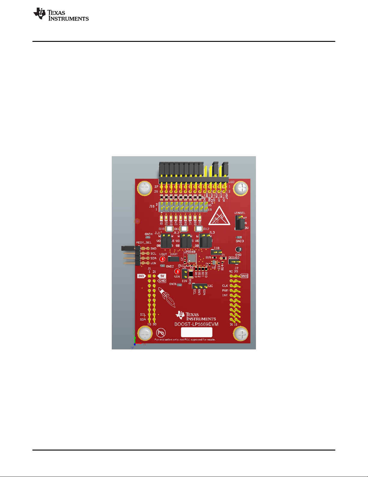
The EVM contains one LP5569 device (see Table 1).
Table 1. Device and Package Configurations
REFERENCE ID DEVICE PACKAGE
U1 LP5569 WQFN (24)
Contents
1 Setup .......................................................................................................................... 3
1.1 Input/Output Connector Description.............................................................................. 3
1.2 I
1.3 LED Type and Supply Selection.................................................................................. 3
1.4 RGB LED Operation................................................................................................ 4
1.5 White LED Operation............................................................................................... 5
1.6 External LED Operation............................................................................................ 6
1.7 EVM and MSP-EXP432P401R LaunchPad Development Kit Setup ........................................ 6
1.8 Minimum Procedure for Turning on the LEDs .................................................................. 8
2 EVM Software................................................................................................................ 9
2.1 EVM Software Installation ......................................................................................... 9
2.2 XDS110 Driver Installation....................................................................................... 14
2.3 EVM Software Launch............................................................................................ 16
2.4 Update Firmware for MSP-EXP432P401R LaunchPad Development Kit ................................. 16
2.5 MSP432 Firmware Running...................................................................................... 18
2.6 Main Menu ......................................................................................................... 18
2.7 Status Bar .......................................................................................................... 18
2.8 Information View................................................................................................... 19
2.9 Register View ...................................................................................................... 19
2.10 Control Menu....................................................................................................... 21
2.11 Control View – Program Tab..................................................................................... 24
2.12 Control View – Code Memory Tab.............................................................................. 25
2.13 Control View – Source Edit Tab................................................................................. 25
2.14 Control View – Log Tab .......................................................................................... 27
2.15 Console............................................................................................................. 27
3 LP5569 Programming ..................................................................................................... 29
3.1 Programming Flow Chart ........................................................................................ 29
3.2 Reserved Keywords............................................................................................... 30
3.3 Commenting ....................................................................................................... 30
3.4 Directives........................................................................................................... 31
3.5 Labels............................................................................................................... 31
3.6 Instruction Set Details ............................................................................................ 32
3.7 Programming Examples.......................................................................................... 34
4 Board Layout................................................................................................................ 38
2
C Address Selection .............................................................................................. 3
SNVU564A–July 2017–Revised August 2017
Submit Documentation Feedback
Using the BOOST-LP5569EVM Evaluation Module
Copyright © 2017, Texas Instruments Incorporated
1
Page 2

5 Schematic ................................................................................................................... 41
6 Bill of Materials (BOM)..................................................................................................... 42
Trademarks
LaunchPad is a trademark of Texas Instruments.
Microsoft, Windows are registered trademarks of Microsoft Corporation.
All other trademarks are the property of their respective owners.
www.ti.com
2
Using the BOOST-LP5569EVM Evaluation Module
Copyright © 2017, Texas Instruments Incorporated
SNVU564A–July 2017–Revised August 2017
Submit Documentation Feedback
Page 3

www.ti.com
1 Setup
This section describes the jumpers and connectors on the EVM as well and how to properly connect, set
up, and use the LP5569EVM. The input voltage range for VINis 2.5 V to 5.5 V. The input voltage range for
V
is 1.65 V to 1.95 V.
1P8
1.1 Input/Output Connector Description
• ADDR_SEL – is provided to configure the I2C slave address.
• DISVIO – is provided to disable the onboard 1.8-V LDO when supplying an external 1.8-V supply.
• I18 – is provided to measure the V1P8 supply current through a 1-Ω sense resistor.
• I2C – is provided to monitor the I2C SDA and SCL signals.
• IIN – is provided to measure the VIN supply current through a 1-Ω sense resistor.
• IOUT – is provided to measure the VOUT supply current. The jumper must be installed for normal
operation.
• J1 and J2 are the TI LaunchPad connector interface.
• JLED – is provided to connect an external LED to the LP5569EVM evaluation module.
• JIS – is provided to measure the LED current through a 1-Ω sense resistor.
• JL1 – is provided to select either a white or RGB LED on LED0, LED1, and LED2 and on the LED
supply.
• JL2 – is provided to select either a white or RGB LED on LED3, LED4, and LED5 and on the LED
supply.
• JL3 – is provided to select either a white or RGB LED on LED6, LED7, and LED8 and on the LED
supply.
• VINSEL – is provided to select 3.3 V either from the MSP432 LaunchPad™ development kit or from an
external supply connected to JLED.
Setup
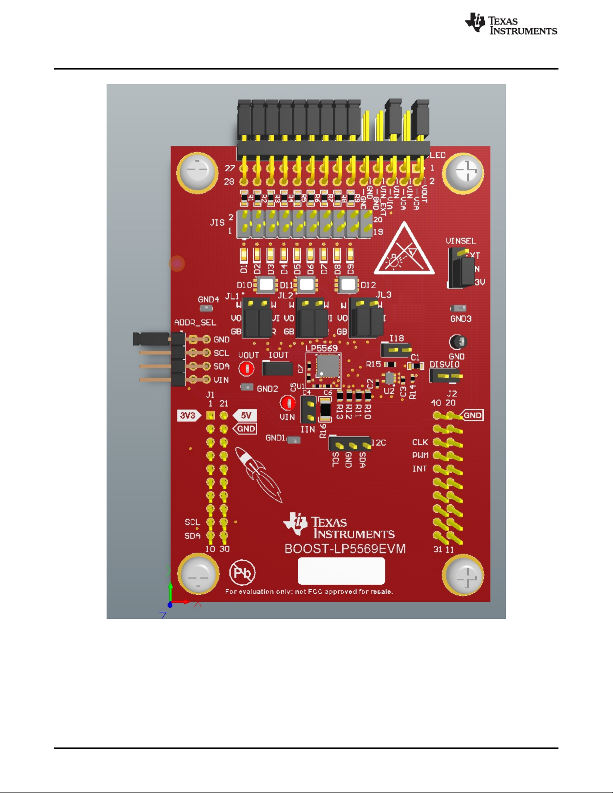
1.2 I2C Address Selection
The LP5569 I2C slave address is set according to the jumper installed on ADDR_SEL.
Figure 1. ADDR_SEL Configuration
1.3 LED Type and Supply Selection
The connectors JL1, JL2, and JL3 are used to select the LED type and supply rail.
Figure 2. JL1, JL2, JL3 Configuration
SNVU564A–July 2017–Revised August 2017
Submit Documentation Feedback
Using the BOOST-LP5569EVM Evaluation Module
Copyright © 2017, Texas Instruments Incorporated
3
Page 4
Setup
www.ti.com
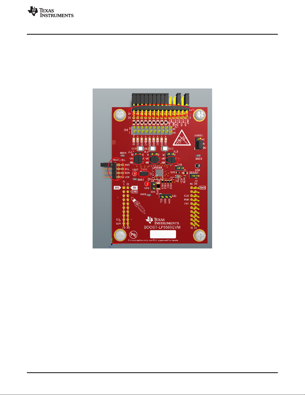
1.4 RGB LED Operation
For proper operation of the LP5569 device, ADDR_SEL, IOUT, JL1, JL2, JL3, JLED, and VINSEL must be
properly configured. The recommended settings, using shunts, are as follows:
• ADDR_SEL: Shunt installed between pins 1 and 2 only.
• IOUT: Shunt installed.
4
Using the BOOST-LP5569EVM Evaluation Module
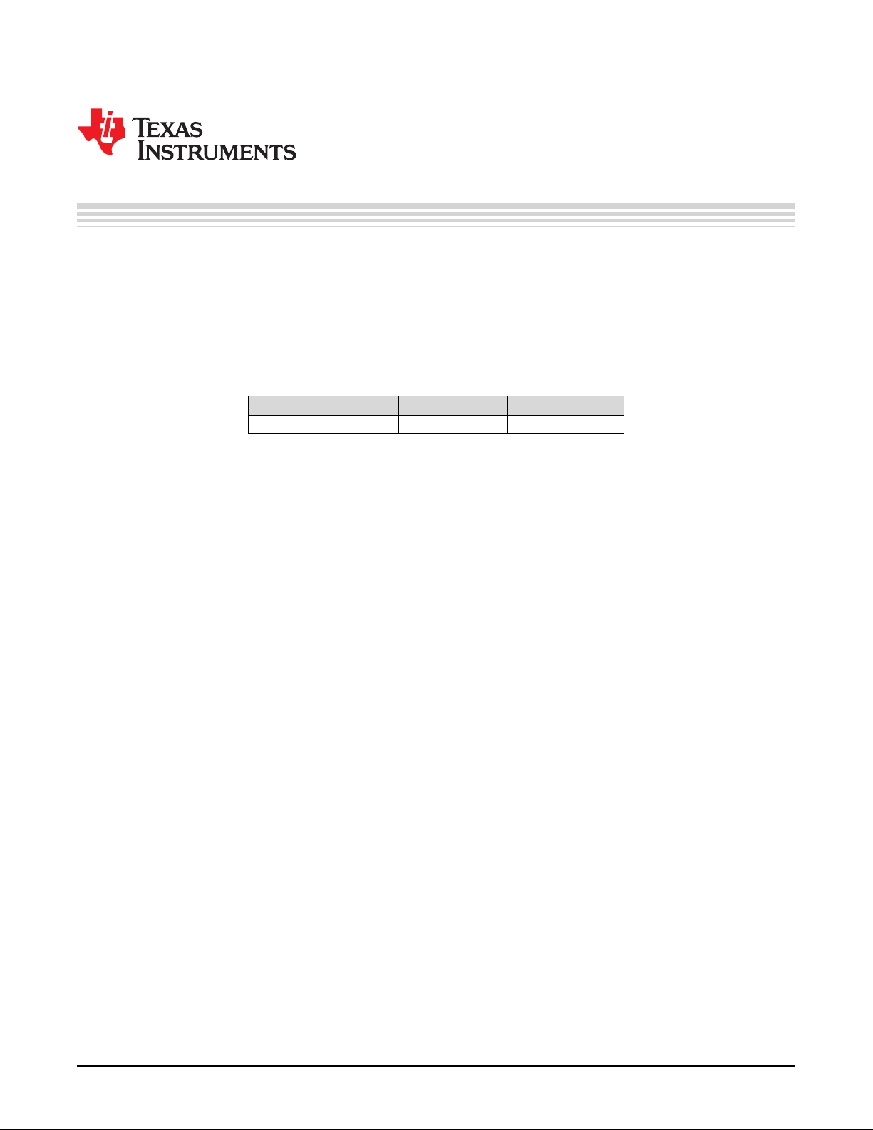
Figure 3. LP5569EVM
Copyright © 2017, Texas Instruments Incorporated
SNVU564A–July 2017–Revised August 2017
Submit Documentation Feedback
Page 5
www.ti.com
• JL1: Shunts installed between pins 3 and 5 and pins 4 and 6 (RGB LED selected).
• JL2: Shunts installed between pins 3 and 5 and pins 4 and 6 (RGB LED selected).
• JL3: Shunts installed between pins 3 and 5 and pins 4 and 6 (RGB LED selected).
• JLED: Shunts installed between pins 1 and 2, 5 and 6, 11 and 12, 13 and 14, 15 and 16, 17 and 18,
In this configuration, the green and blue LEDs are connected to the charge pump output with the red
LEDs connected to VIN.
Setup
19 and 20, 21 and 22, 23 and 24, 25 and 26, 27 and 28.
Figure 4. RGB Configuration Jumper Settings
1.5 White LED Operation
For proper operation of the LP5569 device, ADDR_SEL, IOUT, JL1, JL2, JL3, JLED, and VINSEL must be
properly configured. The recommended settings, using shunts, are as follows:
• ADDR_SEL: Shunt installed between pins 1 and 2 only.
• IOUT: Shunt installed.
• JL1: Shunt installed between pins 1 and 3 (white LED selected).
• JL2: Shunt installed between pins 1 and 3 (white LED selected).
• JL3: Shunt installed between pins 1 and 3 (white LED selected).
• JLED: Shunts installed between pins 1 and 2, 5 and 6, 11 and 12, 13 and 14, 15 and 16, 17 and 18,
19 and 20, 21 and 22, 23 and 24, 25 and 26, 27 and 28.
In this configuration, the white LEDs are connected to the charge pump output.
SNVU564A–July 2017–Revised August 2017
Submit Documentation Feedback
Using the BOOST-LP5569EVM Evaluation Module
Copyright © 2017, Texas Instruments Incorporated
5
Page 6
Setup
www.ti.com
Figure 5. White LED Jumper Settings
1.6 External LED Operation
For proper operation of the LP5569 device, ADDR_SEL, IOUT, JL1, JL2, JL3, JLED, and VINSEL must be
properly configured. The recommended settings, using shunts, are as follows:
• ADDR_SEL: Shunt installed between pins 1 and 2 only.
• IOUT: Shunt installed.
• JL1: No shunt installed.
• JL2: No shunt installed.
• JL3: No shunt installed.
• JLED: No shunt installed, external LED cathodes connected to JLED pins 11, 13, 15, 17, 19, 21, 23,
25, and 27 with LED anodes connected to either JLED pin 1 (VOUT) or pin 3 (VIN).
In this configuration, the LEDs are located on a separate board connected to JLED. Multiple LP5569EVMs can be stacked vertically to control up to 72 LEDs (8 LP5569EVMs) using a single MSP432
LaunchPad developmant kit.
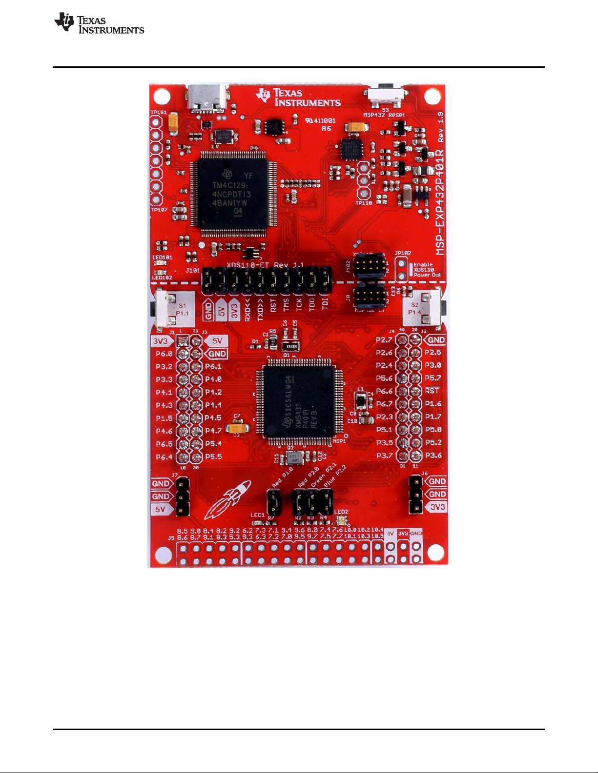
1.7 EVM and MSP-EXP432P401R LaunchPad Development Kit Setup
The MSP-EXP432P401R LaunchPad jumpers should be set as shown in Figure 6.
6
Using the BOOST-LP5569EVM Evaluation Module
Copyright © 2017, Texas Instruments Incorporated
SNVU564A–July 2017–Revised August 2017
Submit Documentation Feedback
Page 7
www.ti.com
Setup
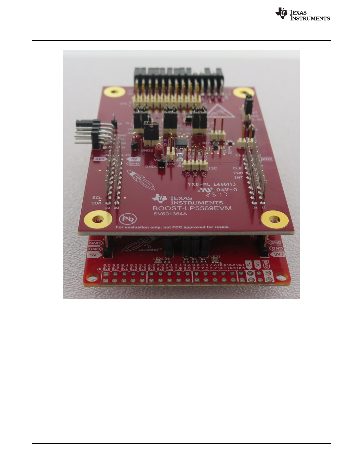
Connect the MSP432 LaunchPad development kit and EVM (BOOSTXL-LP5569) as shown in Figure 7.
SNVU564A–July 2017–Revised August 2017
Submit Documentation Feedback
Figure 6. MSP432 Jumper Settings
Using the BOOST-LP5569EVM Evaluation Module
Copyright © 2017, Texas Instruments Incorporated
7
Page 8
Setup
www.ti.com
Figure 7. Connect Evaluation Board and LaunchPad Development Kit
1.8 Minimum Procedure for Turning on the LEDs
The minimum procedure for turning on the LEDs is as follows:
1. Verify jumper pin settings on the MSP-EXP432P401R LaunchPad development kit and the
LP5569EVM board.
2. Connect the MSP-EXP432P401R LaunchPad to the LP5569EVM board.
3. If it is the first time to use the MSP432, install an XDS110 driver. See the MSP432P401R SimpleLink™
Microcontroller LaunchPad™ Development Kit (MSP‑EXP432P401R) User's Guide for more-detailed
information regarding the XDS110 driver.
4. Verify the XDS110 Class Application/User UART and XDS110 Class Auxiliary Data Port on the
Microsoft®Windows®Device Manager.
5. Install and run the EVM software.
6. If the LaunchPad development kit is a new one or was used another purpose, the EVM software asks
to update the firmware. Update the firmware through the top menu, File → Update Firmware. The EVM
software restarts after updating the firmware.
8
Using the BOOST-LP5569EVM Evaluation Module
Copyright © 2017, Texas Instruments Incorporated
SNVU564A–July 2017–Revised August 2017
Submit Documentation Feedback
Page 9
www.ti.com
7. Make sure the Hardware Connected message appears on the status bar.
8. Select the Control Page Menu and Manual tab.
9. Set the appropriate I2C slave address.
10. Click the EN button to high. (Red color means high.)
11. Set the chip_en bit and click Yes to read all registers.
12. Set cp_mode to 1× mode.
13. Change the pwm[0….8] register values and click the Update button.
2 EVM Software
EVM software is available for download from the Product Folder. The LP5569EVM is connected via USB
to the computer and controlled with special EVM software (Windows 7 and 10 compatible). A
SimpleLink™ MSP432P401R LaunchPad™ Development Kit is used with the EVM to provide I2C
communication and external PWM, EN, and INT pin control with the LP5569 device via USB.
EVM Software
Figure 8. MSP432 LaunchPad Developmant Kit (MSP-EXP432P401R) and LP5569 EVM
2.1 EVM Software Installation
Execute the setup_LP5569_EVM.msi file. If it is compressed in zip file format, unzip first in any location,
and then click the Run button even though the Windows security warning message appears. Click the
Next button.
SNVU564A–July 2017–Revised August 2017
Submit Documentation Feedback
Using the BOOST-LP5569EVM Evaluation Module
Copyright © 2017, Texas Instruments Incorporated
9
Page 10

EVM Software
www.ti.com
Figure 9. Setting Up the LP5569 EVM
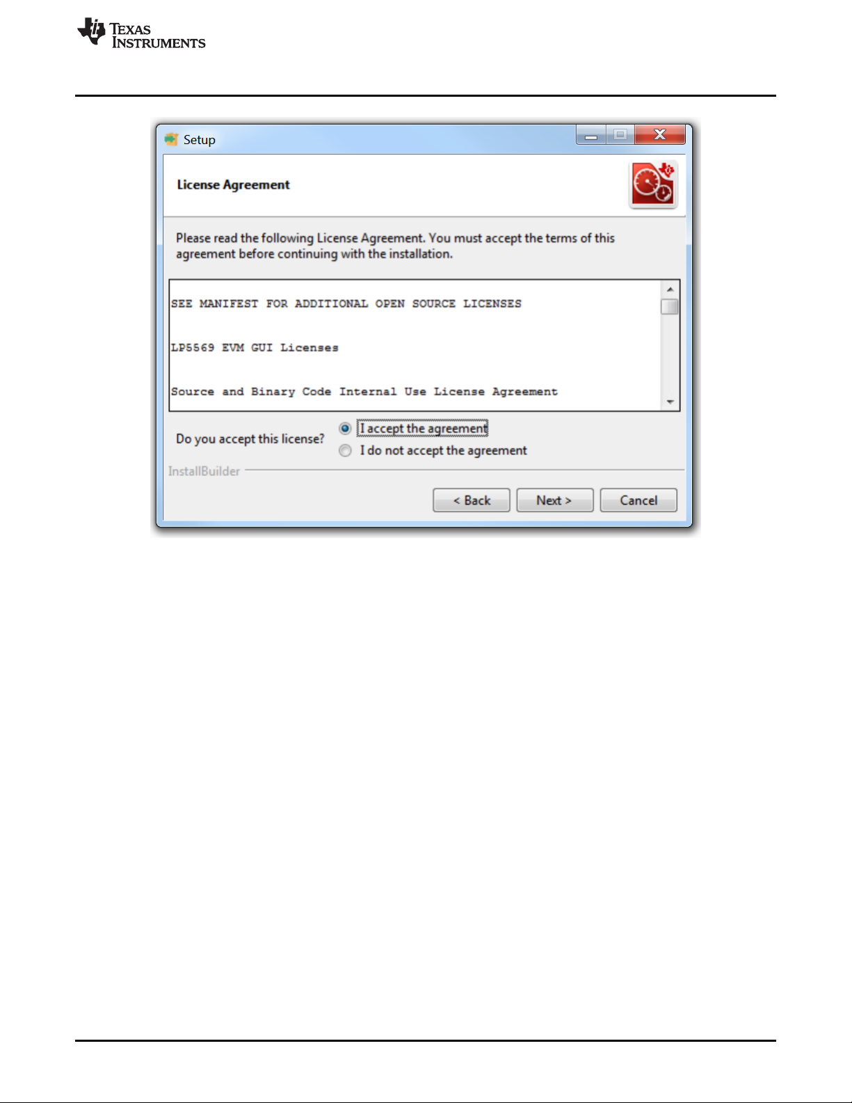
Check to accept the agreement and click the Next button to proceed with the installation.
10
Using the BOOST-LP5569EVM Evaluation Module
Copyright © 2017, Texas Instruments Incorporated
SNVU564A–July 2017–Revised August 2017
Submit Documentation Feedback
Page 11
www.ti.com
EVM Software
Figure 10. License Agreement
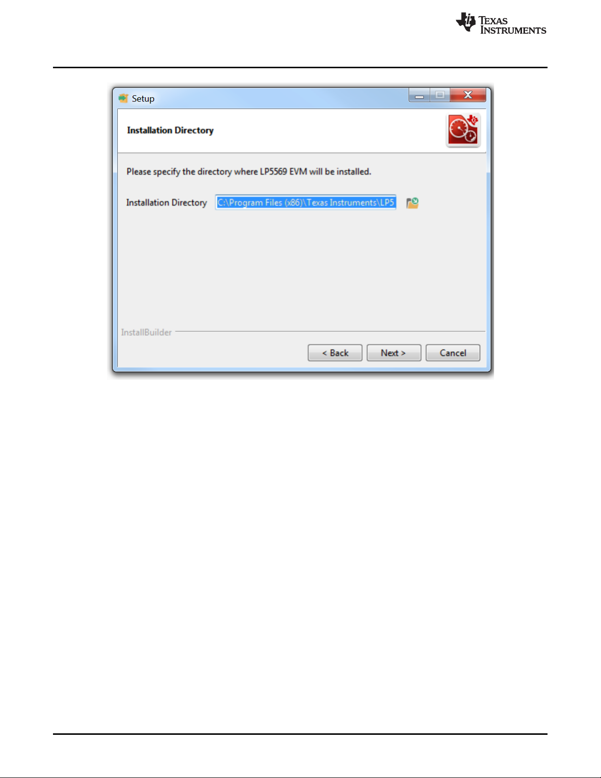
Click Next button. By default, the program is installed in the C:\Program Files (x86)\Texas
Instruments\LP5569 folder and Texas Instruments\LP5569EVM in the start menu.
SNVU564A–July 2017–Revised August 2017
Submit Documentation Feedback
Using the BOOST-LP5569EVM Evaluation Module
Copyright © 2017, Texas Instruments Incorporated
11
Page 12
EVM Software
www.ti.com
Figure 11. Installation Directory Dialog
Click the Next button to proceed with the installation.
12
Using the BOOST-LP5569EVM Evaluation Module
Copyright © 2017, Texas Instruments Incorporated
SNVU564A–July 2017–Revised August 2017
Submit Documentation Feedback
Page 13
www.ti.com
EVM Software
Figure 12. Installation Progress
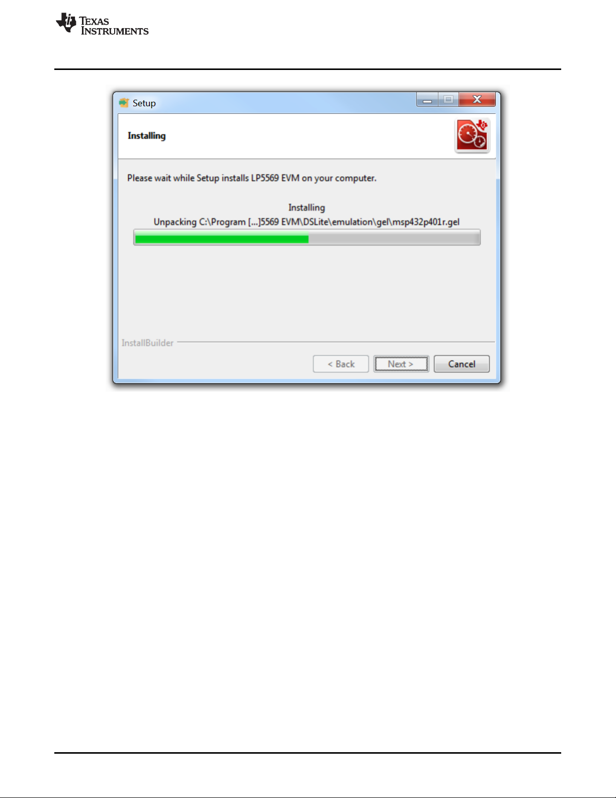
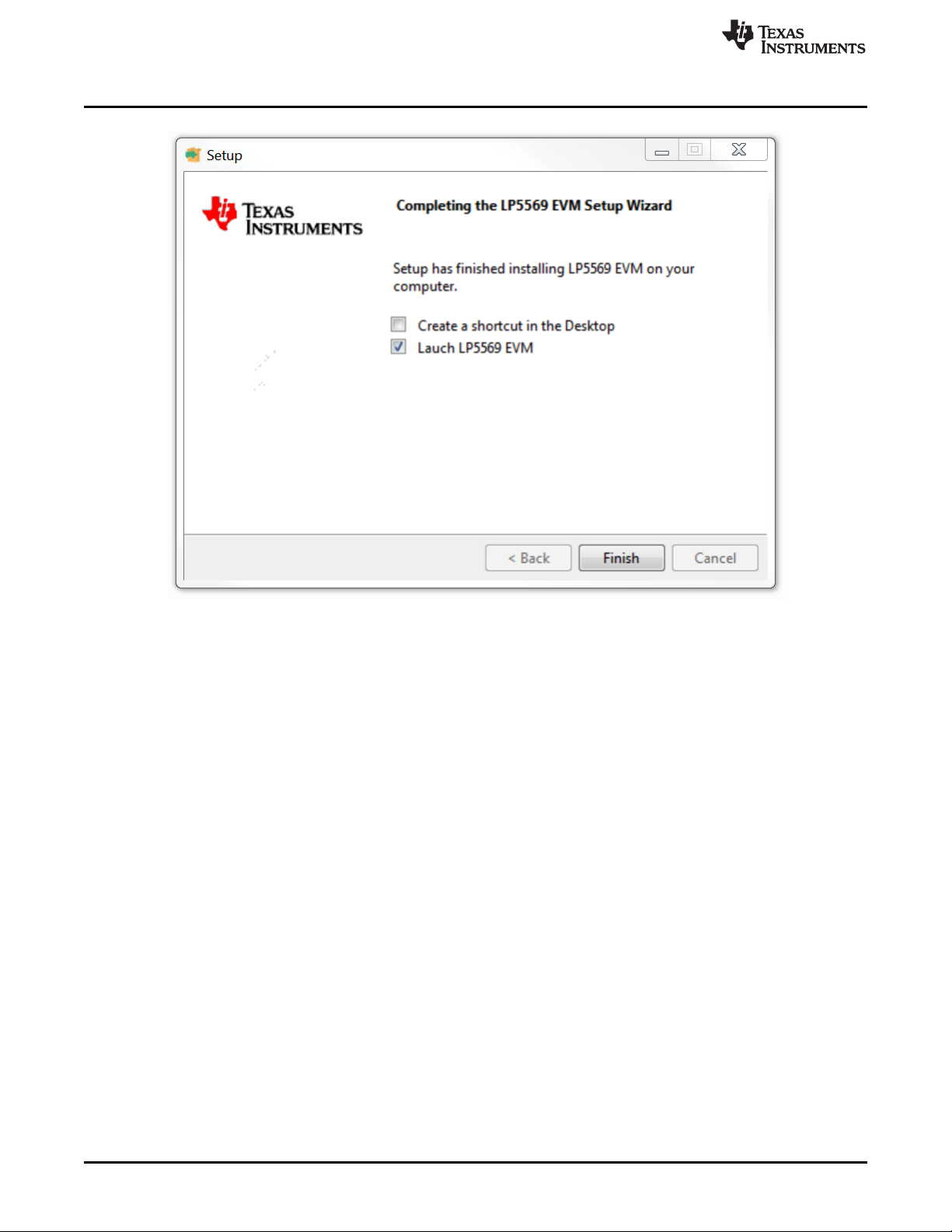
Check to create a desktop icon for the program and check to launch the EVM software after installation.
SNVU564A–July 2017–Revised August 2017
Submit Documentation Feedback
Using the BOOST-LP5569EVM Evaluation Module
Copyright © 2017, Texas Instruments Incorporated
13
Page 14
EVM Software
www.ti.com
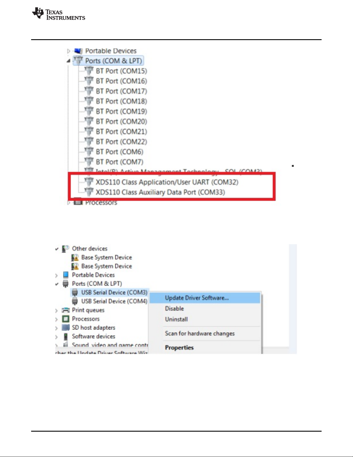
2.2 XDS110 Driver Installation
The EVM software uses XDS110, a back-channel UART-over-USB connection, so it should be installed
properly.
Connect the PC and MSP-EXP432P401R LaunchPad development kit using a USB cable and open the
Device Manager of Windows (Control Panel→Device Manager). Verify that XDS110 Class
Application/User UART and XDS110 Class Auxiliary Data Port appear.
Figure 13. LP5569 Setup Wizard
14
Using the BOOST-LP5569EVM Evaluation Module
Copyright © 2017, Texas Instruments Incorporated
SNVU564A–July 2017–Revised August 2017
Submit Documentation Feedback
Page 15
www.ti.com
EVM Software
Figure 14. Verify XDS110 Driver
If they are shown as USB Serial Device (COMx), the driver must be updated.
Figure 15. Driver Update
The XDS100 driver can be downloaded from XDS Emulation Software Package. If the EVM software is
already installed in your computer, the driver software can be saved in the folder where the EVM software
is already installed. The default EVM software installation folder is C:\Program Files (x86)\Texas
Instruments\LP5569 EVM.
SNVU564A–July 2017–Revised August 2017
Submit Documentation Feedback
Using the BOOST-LP5569EVM Evaluation Module
Copyright © 2017, Texas Instruments Incorporated
15
Page 16

EVM Software
2.3 EVM Software Launch
Run C:\Program Files (x86)\Texas Instruments\ LP5569 EVM\LP5569_EVM.exe if the default installation
folder was not modified in the EVM software installation step or click the desktop icon, LP5569_EVM.
www.ti.com
Figure 16. Driver Installation
Figure 17. Desktop Icon
2.4 Update Firmware for MSP-EXP432P401R LaunchPad Development Kit
The MSP-EXP432P401R LaunchPad development kit can be used for many purposes. Therefore, if the
LaunchPad development kit is a new one or was used for another purpose, the EVM software asks to
update the firmware through a popup window.
16
Using the BOOST-LP5569EVM Evaluation Module
Copyright © 2017, Texas Instruments Incorporated
SNVU564A–July 2017–Revised August 2017
Submit Documentation Feedback
Page 17

www.ti.com
Firmware can be updated through the top menu, FILE → FW Update.
EVM Software
Figure 18. MSP432 Update Firmware
Figure 19. Firmware Update Menu
A firmware-download-status popup is displayed after finishing the firmware update.
Figure 20. Firmware Download Status
The EVM software is restarted after updating the firmware.
SNVU564A–July 2017–Revised August 2017
Submit Documentation Feedback
Using the BOOST-LP5569EVM Evaluation Module
Copyright © 2017, Texas Instruments Incorporated
17
Page 18

EVM Software
2.5 MSP432 Firmware Running
There are three LEDs on the MSP-EXP432P401R LaunchPad development kit, and if the firmware is
working properly, the LED color is usually blue when there is no transaction between the firmware and the
EVM software.
2.6 Main Menu
There are three available views on the main menu: Info, Register, and Control. The components in each
view are synchronized so any changes performed in one view of the menu are automatically updated in
the others.
www.ti.com
Figure 21. MSP432 LED
2.7 Status Bar
The status bar at the bottom of the EVM software screen provides information regarding hardware
connection status, I2C communication status, and software versions. Once the EVM software is connected
to the hardware and starts to communicate with the firmware of the MSP432 LaunchPad development kit,
the light blue sign Hardware Connected is displayed.
18
Using the BOOST-LP5569EVM Evaluation Module
Figure 22. Main Menu Icons
Figure 23. Status Bar (Hardware Connected)
SNVU564A–July 2017–Revised August 2017
Copyright © 2017, Texas Instruments Incorporated
Submit Documentation Feedback
Page 19

www.ti.com
2.8 Information View
The information view is shown when the EVM software is started or the Info icon is clicked, and it provides
brief information about the LP5569 device. For more-detailed information, see LP5569 Nine-Channel I2C
RGB LED Driver With Engine Control and Charge Pump.
EVM Software
2.9 Register View
The register view is shown when the Register icon is clicked, and it provides the register values, field
values, and descriptions.
Figure 24. Information View
SNVU564A–July 2017–Revised August 2017
Submit Documentation Feedback
Using the BOOST-LP5569EVM Evaluation Module
Copyright © 2017, Texas Instruments Incorporated
19
Page 20

EVM Software
www.ti.com
Figure 25. Register View (Collapsed)
Clicking on a bold text entry in the RegisterName column expands the register group to reveal all registers
contained within the RegisterName group. Any RegisterName that is expanded can be collapsed by
clicking on the RegisterName a second time.
20
Figure 26. Register View (Expanded)
Using the BOOST-LP5569EVM Evaluation Module
Copyright © 2017, Texas Instruments Incorporated
SNVU564A–July 2017–Revised August 2017
Submit Documentation Feedback
Page 21

www.ti.com
Enter the desired hex value in the registers (Current Value column), perform a bit-wise configuration of
any register fields by double-clicking on the corresponding register bit, or configure a register field by
entering the desired hex value in the Value column located under FieldView. FieldView displays the
description of all fields of the selected register. Each register can be read independently or all registers
can be read at once by using the Read or Read All button, respectively. The data is written to the
register(s) in one of two ways, depending on the Update Mode field selection: In Immediate mode, the
register data is written immediately following a Current Value , an individual bit, or a Value change. In
Deferred mode, the displayed data is written to all registers on depression of the Write button.
Press the Read All button to read back all the registers and update the values in this table. If any register
value must be changed, simply double-click on the individual bit values to change the value in this table in
immediate updated mode or press the Write Register button to write all the registers at a time if Deferred
is selected instead of Immediate from the drop-down box.
Register settings can be saved in text-file format by selecting Save Registers from file menu.
A register settings file in text-file format can be loaded and programmed automatically by selecting Load
Register from the file menu.
2.10 Control Menu
The Control view is shown when the Control icon is clicked, and provides easy ways to control registers
and pin values.
There are five tabs available under the Control view: Manual, Program, Code Memory, Source Edit, and
Log. The LP5569 registers are grouped by function with the description of each function being displayed in
the lower right quadrant. When hovering the cursor over a check box, a drop-down dialog pops up a field
describing the settings available. The Control view provides immediate mode only, unlike the Registers
view which also provides deferred mode.
EVM Software
2.10.1 Control View – Common Controls
The GUI provides control of I2C slave-address selection, direct register access, EN/PWM pin control, and
the external clock that is common to all five control screen tabs.
Figure 27. Common Controls
• I2C Slave Address Selection
– The I2C slave addresses 0x32, 0x33, 0x34, 0x35, 0x40, 0x42, 0x43, 0x44, and 0x45 are available.
The user must ensure that the slave address selected matches the jumper setting on the EVM
ADDR_SEL header (see Figure 1).
• Direct Register Access
– Register data can be accessed through the direct access group. The EN pin should be in the high
state before reading or writing data though I2C.
• EN/PWM Pin Control
– EN pin control. Red color means high, gray means low.
– The EN pin can be used as PWM, and EVM software supports 500 Hz, 600 Hz, 700 Hz, 800 Hz,
900 Hz, and from 1 kHz to 20 kHz with 1-kHz steps.
– When PWM is unchecked, the frequency, duty cycle, and update controls are gray (inactive). The
PWM checkbox must be checked to activate the PWM signal from the MSP432 LaunchPad
development kit and enable frequency and duty-cycle updates. The Update button must be clicked
after any change to frequency or duty cycle.
• External Clock Control
– External clock pin control. Red color means that a 32.7-kHz external clock is operating.
SNVU564A–July 2017–Revised August 2017
Submit Documentation Feedback
Using the BOOST-LP5569EVM Evaluation Module
Copyright © 2017, Texas Instruments Incorporated
21
Page 22

EVM Software
Figure 28 illustrates the GUI Read all registers prompt which appears after setting the chip_en bit in the
CHIP_EN register.
www.ti.com
Figure 28. Control View (Manual Tab)
2.10.2 Chip Enable and MISC Setting
The chip_en bit of the CONFIG register can be written by clicking the chip_en check box, and a popup
window is shown to read all registers after writing the chip_en bit. Note that the EN pin should be high
before accessing registers. The en_auto_incr bit and powersave_en bit of the MISC register can be
controlled also.
2.10.3 Direct LED Current and PWM Control
There are nine tabs to control each LED from LED0 to LED8. The external_power(x), exp_en(x),
led(x)_ratio_en and mf_mapping(x) bits of the LED(X)_CONTROL register can be controlled. The pwm(x)
bit of the LED(X)_PWM register and the current(x) bit of the LED(X)_CURRENT register can also be
adjusted. Regarding pwm(x) and current(x), an Update button click is required to write data through I2C
after changing the value by using the slide bar or text box.
22
Figure 29. LED ON-OFF Control
Using the BOOST-LP5569EVM Evaluation Module
Copyright © 2017, Texas Instruments Incorporated
SNVU564A–July 2017–Revised August 2017
Submit Documentation Feedback
Page 23

www.ti.com
2.10.4 Charge Pump Control
The charge pump mode, cp_return_1x and cp_dis_dischg settings in registers MISC and MISC2 are
configured within this group.
2.10.5 PWM Control
The PWM group box provides information and control of the CONFIG_PWM register (0x00) and external
PWM signal generation.
EVM Software
Figure 30. Charge Pump Control Information
2.10.6 GPIO Control
The gpo and gpio_config bits of the IO_CONTROL register can be controlled. The check box for gpo is
enabled only when the gpio_config bits are set to 2h or 3h, whereas the Read> button to read the current
status of pin is available only when the gpio_config bits are set to 0h or 1h.
2.10.7 Fault Status
The LED_FAULT1, LED_FAULT2, and GENERAL_FAULT registers can be read by clicking the read
button or selecting the poll check box. The polling time to read the fault registers is 1s.
Figure 31. PWM Register Information
Figure 32. Interrupt Status/Mask/Clear
SNVU564A–July 2017–Revised August 2017
Submit Documentation Feedback
Using the BOOST-LP5569EVM Evaluation Module
Copyright © 2017, Texas Instruments Incorporated
23
Page 24

EVM Software
2.11 Control View – Program Tab
The Program tab on the control view provides the interfaces to load the compiled file, upload or download
a program to or from the device, and control each engine. The Program tab is divided into two parts: the
right part contains the compiled version of the code; the left part contains program execution-engine
controls.
www.ti.com
2.11.1 Load Hex File
The generated *.hex file can be loaded by clicking the Load Hex File button, browsing the file and clicking
Open. The hex data is shown in the Data column and the Code Memory tab. If there are *.src file and *.lst
files in same file path with the *.hex file, more data is displayed in the Label and Code columns and
Source Edit Tab.
2.11.2 Upload to LP5569
The loaded hex data can be uploaded to the chip by clicking the Upload to LP5569 button.
2.11.3 Download From LP5569
The data on the chip can be downloaded to EVM software by clicking the Download from LP5569 button.
2.11.4 Master Operating Mode
The operation mode is set by selecting the desired value on the drop-down box. Operation modes include:
• Disable—Engine operation is disabled and the engines cannot be run.
• Load Program to SRAM—In this mode, writing to program memory is allowed. While one or more
engines are in the load-program mode. all the three engines are placed in Hold until the loading is
complete.. PWM values are also frozen. Program execution continues when all the engines are out of
the load-program mode. The load-program mode resets the program counter of the respective engine.
The load-program mode can be entered from the disabled mode only. Entering the load-program mode
from the run-program mode is not allowed. Note that the load-program mode does not automatically
load the program opened with the Load Hex File button. When using this operation mode, one must
write the program through the Code Memory tab.
• Run Program—This mode executes the instructions stored in the program memory. Execution register
(ENG1_EXEC, and so forth) bits define how the program is executed (hold, step, free run, or execute
Figure 33. Program Tab
24
Using the BOOST-LP5569EVM Evaluation Module
Copyright © 2017, Texas Instruments Incorporated
SNVU564A–July 2017–Revised August 2017
Submit Documentation Feedback
Page 25

www.ti.com
once). The program start address can be programmed into the Program Counter (PC) register. The
program counter is reset to zero when the upper limit value of the PC is reached.
• Halt—In this mode, instruction execution aborts immediately and engine operation halts. Execution can
be continued if the operation mode is set to Run again.
2.11.5 Run Mode for Engines 1, 2, and 3
Each LED engine has four execution modes. The execution mode is selected by clicking one of the four
push-buttons. Functions of the buttons from left to right are:
• Hold—Engine execution is stopped. The current instruction is executed and then execution stops.
• Step—Execute the instruction at the location pointed to by the program counter, increment the program
counter by 1 and then reset ENG1_EXEC bits to 00 (enter the hold mode).
• Free Run—Start program execution from the instruction pointed to by the program counter.
• Execute Once—Execute the instruction pointed to by the current program counter value and reset.
ENG1_EXEC to 00 (for example, enter Hold mode). The difference between Step and Execute Once is
that Execute Once does not increment the program counter.
2.12 Control View – Code Memory Tab
The Code Memory tab on the control view provides the interfaces to read or write data from or to SRAM
pages.
EVM Software
Figure 34. Code Memory Tab
The code memory tab supports read/write to a single page or read/write of all pages. These operations
are described in the following list:
• Read Page—A single page can be read from the device. Select the row of the desired page and click
the Read Page button.
• Write Page—A single page can be written to the device. Select the row of the desired page and click
the Write Page button.
• Read All Pages—All pages from 0 to 15 can be read by clicking the Read All Pages button.
• Write All Pages — All pages from 0 to 15 can be written by clicking the Write All Pages button.
2.13 Control View – Source Edit Tab
The Source Edit tab on the control view provides the interfaces to create or edit a source file and compile.
SNVU564A–July 2017–Revised August 2017
Submit Documentation Feedback
Copyright © 2017, Texas Instruments Incorporated
Using the BOOST-LP5569EVM Evaluation Module
25
Page 26

EVM Software
www.ti.com
Figure 35. Source Edit Tab
2.13.1 New Source File
A new source file can be created by clicking the New button, browsing to a folder, selecting the file name
and clicking Save. The default target folder is C:\Users\[User Name]\Documents\Texas
Instruments\lp5569.
2.13.2 Load Source File
An existing source file can be loaded by clicking the Load button, browsing to the folder, selecting the file
name and clicking Open. The default target folder is C:\Users\[User Name]\Documents\Texas
Instruments\lp5569.
2.13.3 Save (As) Source File
An edited source file can be saved by clicking the Save button. The Save As button saves the file under a
new name.
2.13.4 Compile Source File
An edited or loaded source file can be compiled by clicking the Save and Compile button. The result of
compilation from the assembler (lasm.exe) is displayed on the Compile Log area.
2.13.5 Input Instruction
A source file can be edited using the interfaces on the Input Instruction group.
26
Using the BOOST-LP5569EVM Evaluation Module
Figure 36. File List After Compilation
Copyright © 2017, Texas Instruments Incorporated
SNVU564A–July 2017–Revised August 2017
Submit Documentation Feedback
Page 27

www.ti.com
• Seg/Label supports predefined label names and .segment directives. If a .segment directive is
selected, the Instruction supports only three options (program1, program2, program3).
• Instruction provides all available instructions. If an instruction is selected, parameter1, parameter2, and
parameter3 are enabled according to the type of instruction and the available parameters should be
provided. The detailed instruction format and examples are displayed.
2.13.6 Line Clear
The selected line is cleared but not removed.
2.13.7 Line Remove
The selected line is cleared and removed.
2.13.8 Line Insert
Seg/Label, Instruction, Parameters, and Comment data are inserted into the selected line.
2.13.9 Line Replace
The selected line is replaced by the Seg/Label, Instruction, Parameters, and Comment data.
2.14 Control View – Log Tab
The Log tab on the control view provides the history regarding I2C read/write, file access, and so forth.
EVM Software
2.15 Console
A predefined macro file can be executed using the Console window (see Figure 38). The Console window
can be opened by selecting Help→Console. The predefined macro file should be saved in .txt file format,
and it can be loaded and executed by clicking the Load File button. The default folder path is
C:\Users\[ID]\Documents\Texas Instruments\ lp5569.
MACRO SYNTAX FUNCTION EXAMPLE
REGISTER_NAME()
REGISTER_NAME(hex_data)
FIELD_NAME()
SNVU564A–July 2017–Revised August 2017
Submit Documentation Feedback
Figure 37. Log Tab
Table 2. Macro Instructions
Register read REGISTER_NAME must be
the same as the register map on the GUI
(see Figure 26)
Register write REGISTER_NAME must be
the same as the register map on the GUI
Field read FIELD_NAME must be same
as the register map on the GUI
Using the BOOST-LP5569EVM Evaluation Module
Copyright © 2017, Texas Instruments Incorporated
>CONFIG(); read CONFIG(0x00) register
CONFIG(0x40); write CONFIG
exp_en0(); read exp_en0 bit
27
Page 28

EVM Software
Table 2. Macro Instructions (continued)
MACRO SYNTAX FUNCTION EXAMPLE
FIELD_NAME(hex_data)
read_all() Read all registers read_all(); real all registers from chip
i2c_addr(hex_addr) Set slave address i2c_addr(0x32); use 0x32 slave address
en_pin(high/low Enable pin control to low or high
ext_clk(on/off) External clock control to on or off
wait(time_ms) Wait time in ms wait(1000); wait 1s
repeat(number_of_loop) { …… } Loop for repeated macro execution
Field write FIELD_NAME must be same
as the register map on the GUI
exp_en0(0x1); write exp_en0 bit
en_pin(high); set en pin to high
en_pin(low); set en pin to low
ext_clk(on); set ext_clk on ext_clk(off); set
ext_clk off
repeat(10); repeat 10 times {en_pin(high);
en pin set to high chip_en(0x01); set
chip_en bit to 1 read_all(); read all
regsiters wait(1000); en_pin(low); en pin
set to low}
www.ti.com
28
Figure 38. Console Window
Figure 39. Macro File
Using the BOOST-LP5569EVM Evaluation Module
Copyright © 2017, Texas Instruments Incorporated
SNVU564A–July 2017–Revised August 2017
Submit Documentation Feedback
Page 29

www.ti.com
3 LP5569 Programming
3.1 Programming Flow Chart
Figure 40 shows the typical programming flow of the LP5569 device. The program is first typed in with the
Source Edit tab of the EVM software or with the PSPad (or equivalent) text editor (See AN-2227 LP5523
Evaluation Kit regarding PSPad usage.) Then the program is compiled into hex and binary files. Finally,
the hex file is loaded into the LP5569 memory and tested.
LP5569 Programming
SNVU564A–July 2017–Revised August 2017
Submit Documentation Feedback
Figure 40. Programming Flow Chart
Using the BOOST-LP5569EVM Evaluation Module
Copyright © 2017, Texas Instruments Incorporated
29
Page 30

LP5569 Programming
3.2 Reserved Keywords
The names of registers and instructions are assembler-reserved keywords. For the LP5523 device, the
following words are reserved and may not be used as statement labels:
Register names :
• ra
• rb
• rc
• rd
Instructions:
• add
• branch
• end
• int
• je
• jge
• jl
• jne
• ld
• load_addr
• load_end
• load_next
• load_prev
• load_start
• map_addr
• map_clr
• map_next
• map_prev
• map_sel
• map_start
• ramp
• rst
• set_pwm
• sub
• trig_clear
• trigger
• wait
Directives:
• ds
• dw
• .segment
www.ti.com
3.3 Commenting
Commenting starts with a semicolon (;). The assembler ignores all characters after a semicolon.
30
Using the BOOST-LP5569EVM Evaluation Module
Copyright © 2017, Texas Instruments Incorporated
SNVU564A–July 2017–Revised August 2017
Submit Documentation Feedback
Page 31

www.ti.com
3.4 Directives
The directives are not translated directly in the LP5569 device. Instead, directives are instructions for the
LASM.exe assembler. Directives are used to adjust the location of the engine 1, 2, and 3 programs in
memory and reserve memory resources in the LP5569 SRAM. For example, .segment program1 is a
directive which tells the assembler that whatever follows is the program for the program execution
engine 1. An overview of the directives is given in the following table.
.segment Adjust the location of the programs in
ds Define Storage. The directive reserves
dw Define constant Word. Inserts a binary
LP5569 Programming
Table 3. Directives
DIRECTIVE DESCRIPTION EXAMPLE SOURCE CODE
SRAM. Note the leading dot
segment name of engine1 is program1
segment name of engine2 is program2
segment name of engine3 is program3
memory resources in the SRAM. The ds
directive takes one parameter, which is
the number of words to reserve. The
number of bits in a word (word length) is
16. The allocated words are initialized with
zeros.
word to the SRAM.
.segment program1
.segment program2
.segment program3
ds 3
ds 17
dw 0000000011111111b
dw FFABh
dw 3
3.5 Labels
A label is a symbolic address. Labels are used to mark program line(s), like in a branch instruction or
when labeling rows in amapping table. Labels must have the colon (:) suffix.
INSTRUCTION
ramp time, PWM
Time is a positive
constant (0.000484 ×
PWM); PWM is a
positive or negative
constant (–255 to 255).
Note: time is rounded by
the assembler if needed.
ramp var1, prescale,
var2
Var1 is a variable (ra, rb,
rc, rd); Prescale is a
boolean constant (pre=0
or pre=1); Var2 is a
variable (ra, rb, rc, rd).
set_pwm PWM
PWM is a constant
(0–255 or 0–FFh).
set_pwm var1
Var1 is a variable (ra, rb,
rc, rd).
wait time
Time is a positive
constant (0 to 0.484).
Note: time is rounded by
assembler if needed.
SYNTAX
Table 4. LED Driver Instructions
FUNCTION EXAMPLE 16-BIT ASSEMBLED
Output PWM with
increasing or decreasing
duty cycle.
Output PWM with
increasing or decreasing
duty cycle.
Generate a continuous
PWM output.
Generate a continuous
PWM output.
Pause for some time. wait 0.25;
ramp 0.6, 255;
Ramp up to full scale
over 0.6 s.
ramp 1.2, –255;
Ramp down to zero over
1.2 s.
ld ra, 31 ld rb, 255 ramp
ra, pre=0, +rb;
Ramp up to full scale
over 3.9 s.
ld ra, 1; ld rb, 255p;
ramp ra, pre=0, -rb;
Ramp down to zero over
0.12 s.
set_pwm 128;
Set PWM duty cycle to
50%.
ld rc, 128; set_pwm rc;
Set PWM duty cycle to
50%.
Wait 0.25 seconds.
BIT SEQUENCE
0000 1010 1111 1111 0AFF
0001 0101 1111 1111 15FF
1000 0100 0000 0001 8401
1000 0100 0001 0001 8411
0100 0000 1000 0000 4080
1000 0100 0110 0010 8462
0110 0000 0000 0000 6000
ASSEMBLED CODE
(HEX)
SNVU564A–July 2017–Revised August 2017
Submit Documentation Feedback
Using the BOOST-LP5569EVM Evaluation Module
Copyright © 2017, Texas Instruments Incorporated
31
Page 32

LP5569 Programming
3.6 Instruction Set Details
Instructions are executable statements. The LASM assembler translates text-based language source
instructions into hex-based executable codes. This section provides the syntax with detailed examples for
all the LP5569 instructions supported by the LASM assembler.
www.ti.com
Table 5. LED Mapping Instructions
INSTRUCTION
SYNTAX
load_start address
Address is a label which
specifies where to find
the first row.
map_start address
Address is a label which
specifies where to find
the first row.
load_end address
Address is a label which
specifies where to find
the first row.
map_sel output
Output is a constant (0
to 9); 10 through 127 =
no drivers selected.
map_clr Clears engine-to-driver
map_next Sets the next row active
map_prev Sets the previous row
load_next The index pointer is set
load_prev The index pointer is set
load_addr address
Address is a label which
specifies the row to
which the pointer is to
be moved.
map_addr address
Address is a label which
specifies the row to
which the pointer is to
be moved.
FUNCTION EXAMPLE 16-BIT ASSEMBLED
Defines the start
address of the mappingdata table. The
mapping-data-table start
address is restricted to
the lower half of
memory.
Defines the start
address of the mappingdata table and sets the
row active.
Defines the last address
of the mapping-data
table. The mappingdata-table end address
is restricted to the lower
half of memory.
Connects one and only
one LED output to an
engine.
mapping.
in the mapping table.
active in the mapping
table.
to point to the next row
in the mapping-data
table.
to point to the previous
row in the mapping-data
table.
Sets the index pointer to
point to the mappingdata-table row defined
by address. An SRAM
address containing
mapping data is
restricted to lower half of
memory.
Sets the index pointer to
point to the mappingdata-table row defined
by address and sets the
row active. An SRAM
address containing
mapping data is
restricted to lower half of
memory.
BIT SEQUENCE
load_start row1 ;
The first row can be
found at the address
marked with row1.
map_start row1 ;
The first row can be
found at the address
marked with row1.
load_end row9 ;
The last row can be
found at the address
marked with row9.
map_sel 1 ;
D1 output is connected
to the engine.
map_clr 1001 1101 0000 0000 9D00
map_next 1001 1101 1000 0000 9D80
map_prev 1001 1101 1100 0000 9DC0
load_next 1001 1101 1000 0000 9D81
load_prev 1001 1101 1100 0000 9DC1
load_addr row2 1001 1111 0000 0001 9F01
map_addr row2 1001 1111 1000 0001 9F81
1001 1110 0000 0000
Assumed that row1
points to addr 00h.
1001 1100 0000 0000 9C00
1001 1100 1000 1000 9C88
1001 1101 0000 0001 9D01
ASSEMBLED CODE
9E00
(HEX)
32
Using the BOOST-LP5569EVM Evaluation Module
Copyright © 2017, Texas Instruments Incorporated
SNVU564A–July 2017–Revised August 2017
Submit Documentation Feedback
Page 33

www.ti.com
LP5569 Programming
Table 6. Branch Instructions
INSTRUCTION
SYNTAX
rst Resets program counter
branch loopcount,
address
Loopcount is a constant
(0 to 63); address is a
label which specifies the
offset.
int Causes an interrupt. int 1100 0100 0000 0000 C400
end interrupt, reset
Interrupt (i) is an
optional flag. Reset (r) is
an optional flag.
trigger
w{source1|source2...}
Source is the source of
the trigger (1, 2, 3,
external).
trigger
s{target1|target2...}
Source is the source of
the trigger (1, 2, 3,
extenal ).
trig_clear Clear pending triggers. trig_clear 1110 0000 0000 0000 E000
jne var1, var2, address
var1 is a variable (ra, rb,
rc, rd);
var2 is a variable (ra, rb,
rc, rd);
address is a label which
specifies the offset.
jl var1, var2, address
var1 is a variable (ra, rb,
rc, rd);
var2 is a variable (ra, rb,
rc, rd);
address is a label which
specifies the offset.
jge var1, var2, address
var1 is a variable (ra, rb,
rc, rd);
var2 is a variable (ra, rb,
rc, rd);
address is a label which
specifies the offset
je var1, var2, address
var1 is a variable (ra, rb,
rc, rd);
var2 is a variable (ra, rb,
rc, rd);
address is a label which
specifies the offset.
FUNCTION EXAMPLE 16-BIT ASSEMBLED
and starts the program
again.
Repeat a section of
code. A branch to the
outside of a segment is
not allowed.
End program execution. end i;
Wait for a trigger. trigger w{1};
Send a trigger. trigger s{1};
Jump if not equal. It
jumps forward to the
address relative to the
present location.
Jump if less. It jumps
forward to the address
relative to the present
location.
Jump if greater or equal.
It jumps forward to the
address relative to the
present location.
Jump if equal. It jumps
forward to the address
relative to the present
location.
rst 0000 0000 0000 0000 0000
branch 20, loop1;
Define loop for 20 times.
End program execution
and send an interrupt.
Wait for a trigger from
engine 1.
Send a trigger to engine
1
jne ra, rb, flash;
jump to flash if A!=B.
jl ra, rb, flash;
jump to flash if A<B
jge ra, rb flash;
jump to flash if A>=B.
je ra, rb, flash;
jump to flash if A==B
BIT SEQUENCE
1010 1010 0000 0000 AA00
1101 0000 0000 0000 D000
1110 0000 1000 0000 E080
1110 0000 0000 0010 E002
1000 1000 0010 0001
Assumes that offset = 2.
1000 1010 0001 0001
Assumes that offset = 1.
1000 1100 0001 0001
Assumes that offset = 1.
1000 1110 0001 0001
Assumes that offset = 1.
ASSEMBLED CODE
8821
8A11
8C11
8E11
(HEX)
SNVU564A–July 2017–Revised August 2017
Submit Documentation Feedback
Using the BOOST-LP5569EVM Evaluation Module
Copyright © 2017, Texas Instruments Incorporated
33
Page 34

LP5569 Programming
www.ti.com
Table 7. Data Transfer and Arithmetic Instructions
INSTRUCTION
SYNTAX
ld var, value
var is a variable (ra, rb,
rc);
value is a constant (0 to
255 or 0 to FFh)
add var, value
var is a variable (ra, rb,
rc);
value is a constant (0 to
255 or 0 to FFh)
add var1, var2, var3
var1 is a variable (ra, rb,
rc);
var2 is a variable (ra, rb,
rc, rd);
var3 is a variable (ra, rb,
rc, rd).
sub var, value
var is a variable (ra, rb,
rc);
value is a constant (0 to
255 or 0 to FFh)
sub var1, var2, var3
var1 is a variable (ra, rb,
rc);
var2 is a variable (ra, rb,
rc, rd);
var3 is a variable (ra, rb,
rc, rd).
FUNCTION EXAMPLE 16-BIT ASSEMBLED
Assigns a value to a
variable
Add the 8-bit value to
the variable value.
Add the value of var3 to
the value of var2 and
store the result in var1.
Subtract the 8-bit value
from the variable value.
Subtract the value of
var3 from the value of
var2 and store the result
in var1.
ld ra, 10;
Variable A = 10.
add ra, 30;
A = A + 30.
add ra, rc, rd;
A = C + D.
sub ra, 30;
A = A – 30
sub ra, rc, rd;
A = C – D
BIT SEQUENCE
1001 0000 0000 1010 900A
1001 0001 0001 1110 911E
1001 0011 0000 1010 930B
1001 0010 0001 1110 921E
1001 0011 0001 1011 931B
ASSEMBLED CODE
(HEX)
3.7 Programming Examples
This is a demonstration example to display a slow ramp of all three colors for each tri-color LED.
Label/Seg INSTRUCTION PARAMETERS
ENG1: dw 0000 0001 0001 0001b
ENG2: dw 0000 0000 1000 1100b
ENG3: dw 0000 0000 0110 0010b
ALL: dw 0000 0001 1111 1111b
.segment program1
loop1:
.segment program2
Table 8. Example .src file
map_addr ALL
set_pwm 0
map_addr ENG1
trigger s{2|3}
ramp 2, 255
ramp 2, –255
ramp 2, -255
branch 0, loop1
rst
trigger w{1}
map_addr ENG2
34
Using the BOOST-LP5569EVM Evaluation Module
SNVU564A–July 2017–Revised August 2017
Submit Documentation Feedback
Copyright © 2017, Texas Instruments Incorporated
Page 35

www.ti.com
loop2:
.segment program3
loop3:
LP5569 Programming
Table 8. Example .src file (continued)
ramp 2, –255
ramp 2, 255
ramp 2, –255
branch 0, loop2
rst
trigger w{1}
map_addr ENG3
ramp 2, –255
ramp 2, –255
ramp 2, 255
branch 0, loop3
rst
SNVU564A–July 2017–Revised August 2017
Submit Documentation Feedback
Using the BOOST-LP5569EVM Evaluation Module
Copyright © 2017, Texas Instruments Incorporated
35
Page 36

LP5569 Programming
.hex file: The .src file is translated to the following .hex file by the assembler (lasm.exe).
www.ti.com
.lst file: The .lst file is generated by the assembler (lasm.exe). The listing file contains the source code
along with the compiled machine code and is helpful for debugging and seeing how source code is
translated into machine code. The first column is the row number, the second column indicates the SRAM
memory address, the third column shows the machine code data and the fourth column includes the
source code.
001 ; This is a demonstration to
002 ; ramp of all 3 colors for each
003
004 00 0111 ENG1: dw 0000 0001 0001 0001b
005 01 008C ENG2: dw 0000 0000 1000 1100b
006 02 0062 ENG3: dw 0000 0000 0110 0010b
007
36
Using the BOOST-LP5569EVM Evaluation Module
display a slow
tri-color LED
Figure 41. Example .hex File
Table 9. Example .lst File
SNVU564A–July 2017–Revised August 2017
Submit Documentation Feedback
Copyright © 2017, Texas Instruments Incorporated
Page 37

www.ti.com
008 03 01FF ALL: dw 0000 0001 1111 1111b
009
010 .segment program1
011 04 9F83 map_addr ALL
012 05 4000 set_pwm 0
013 06 9F80 map_addr ENG1
014 07 E00C trigger s{2|3}
015 loop1:
016 08 20FF ramp 2, 255
017 09 21FF ramp 2, –255
018 0A 21FF ramp 2, –255
019 0B A004 branch 0, loop1
020 0C 0000 rst
021
022 program2
023 0D E080 trigger w{1}
024 0E 9F81 map_addr ENG2
025 loop2:
026 0F 21FF ramp 2, –255
027 10 20FF ramp 2, 255
028 11 21FF ramp 2, –255
029 12 A002 branch 0, loop2
030 13 0000 rst
031
032 .segment program3
033 14 E080 trigger w{1}
034 15 9F82 map_addr ENG3
035 loop3:
0326 16 21FF ramp 2, –255
037 17 21FF ramp 2, –255
038 18 20FF ramp 2, 255
039 19 A002 branch 0, loop3
040 1A 0000 rst
LP5569 Programming
Table 9. Example .lst File (continued)
========================
========
Labels:
ENG1 = 00
ENG2 = 01
ENG3 = 02
ALL = 03
loop1 = 08
loop2 = 0F
loop3 = 16
========================
========
Segments:
program1 = 04
program2 = 0D
SNVU564A–July 2017–Revised August 2017
Submit Documentation Feedback
Using the BOOST-LP5569EVM Evaluation Module
Copyright © 2017, Texas Instruments Incorporated
37
Page 38

Board Layout
program3 = 14
========================
========
Free memory: 228
Errors: 0
4 Board Layout
www.ti.com
Table 9. Example .lst File (continued)
38
Figure 42. Top Assembly Layer
Using the BOOST-LP5569EVM Evaluation Module
Copyright © 2017, Texas Instruments Incorporated
SNVU564A–July 2017–Revised August 2017
Submit Documentation Feedback
Page 39

www.ti.com
Board Layout
Figure 43. Top Layer Routing
SNVU564A–July 2017–Revised August 2017
Submit Documentation Feedback
Figure 44. Middle Layer 1 Routing
Using the BOOST-LP5569EVM Evaluation Module
Copyright © 2017, Texas Instruments Incorporated
39
Page 40

Board Layout
www.ti.com
Figure 45. Middle Layer 2 Routing
40
Figure 46. Bottom Layer Routing (Mirrored)
Using the BOOST-LP5569EVM Evaluation Module
Copyright © 2017, Texas Instruments Incorporated
SNVU564A–July 2017–Revised August 2017
Submit Documentation Feedback
Page 41

www.ti.com
5 Schematic
Schematic
Figure 47. LP5569EVM Schematic
SNVU564A–July 2017–Revised August 2017
Submit Documentation Feedback
Using the BOOST-LP5569EVM Evaluation Module
Copyright © 2017, Texas Instruments Incorporated
41
Page 42

Bill of Materials (BOM)
6 Bill of Materials (BOM)
DESIGNATOR QTY. VALUE DESCRIPTION
C1 1 10 µF
C2, C3, C4, C5,
C6, C7
D1, D2, D3, D4,
D5, D6, D7, D8,D99
D10, D11, D12 3 RGB LED, RGB, SMD
H1, H2, H3, H4 4
H5, H6, H7, H8 4 Standoff, hex, 0.5"L #4-40 nylon Standoff 1902C Keystone
J1 1 Receptacle, 2,54 mm, 10 × 2, tin, TH
J2 1 Receptacle, 2,54 mm, 10 × 2, tin, TH
J3, J4 2 Header, 100-mil, 3 × 1, gold, TH 3 × 1 header TSW-103-07-G-S Samtec
J5 1 Header, 2.54 mm, 4 × 2, gold, R/A, TH
J6, J7, J8, J9 4 Header, 100-mil, 2 × 1, gold, TH 2 × 1 header TSW-102-07-G-S Samtec
J10 1 Header, 10 × 2, 2,54 mm, tin, TH
6 1 µF
Cool
white
www.ti.com
Table 10. LP556EVM BOM
PACKAGE
REFERENCE
Capacitor, ceramic, 10 µF, 6.3 V, ±10%,
JB, 0603
Capacitor, ceramic, 1 µF, 6.3 V, ±10%,
X5R, 0402
LED, cool white, SMD 0603 LED LNJ037X8ARA Panasonic
Machine screw, round, #4-40 × 1/4,
nylon, philips panhead
0603 C1608JB0J106K080AB TDK
0402 GRM155R60J105KE19D MuRata
LED, 3- × 2- ×
3.6-mm
Screw NY PMS 440 0025 PH
10 × 2
receptacle
10 × 2
receptacle
Header, 2,54-
mm, 4 × 2, R/A,TH61300821021 Wurth Elektronik
Header, 10 × 2,
2,54 mm, tin,THTSW-110-07-T-D Samtec
PART NUMBER MANUFACTURER
ASMT-YTC2-0AA02 Avago
B&F Fastener
Supply
SSQ-110-03-T-D Samtec
SSQ-110-03-T-D Samtec
J11, J12, J13 3 Header, 100-mil, 3 × 2, gold, TH 3 × 2 header TSW-103-07-G-D Samtec
J14 1 Header, 100-mil, 14 × 2, gold, R/A, TH
R1, R2, R3, R4,
R5, R6, R7, R8,R99 1.00 Resistor, 1.00 Ω, 1%, 0.1 W, 0603 0603 CRCW06031R00FKEA Vishay-Dale
R10, R11, R12,
R13
R14 1 1.0 kΩ Resistor, 1.0 kΩ, 5%, 0.063 W, 0402 0402 CRCW04021K00JNED Vishay-Dale
R15 1 1.00 Ω Resistor, 1.00 Ω, 1%, 0.1 W, 0603 0603 CRCW06031R00FKEA Vishay-Dale
R16 1 1.00 Ω Resistor, 1.00 Ω, 1%, 0.5 W, 1206 1206 CSR1206FK1R00
SH1, SH2,
SH3, SH4,
SH4, SH6,
SH7, SH8,
SH9, SH10,
SH11, SH12,
SH13, SH14,
SH15, SH16,
SH17, SH18,
SH19, SH20
TP1, TP2 2 Test point, miniature, red, TH
TP3, TP4, TP5,
TP6
TP7 1 Test point, miniature, black, TH
U1 1
U2 1
4 6.04 kΩ Resistor, 6.04 kΩ, 1%, 0.1 W, 0603 0603 CRCW06036K04FKEA Vishay-Dale
20 1 × 2 Shunt, 100 mil, flash gold, black
4 Header, 1 × 1, tin, TH
Easy-to-use nine-channel RGB LED
driver, RTW0024B (WQFN-24)
Micropower, 150-mA low-dropout CMOS
voltage regulator, 5-pin SC-70, Pb-free
14 × 2 R/A
header
Closed-top 100-
mil shunt
Red miniature
test point
Header, 1 × 1,
50-mil, TH
Black miniature
test point
RTW0024B LP5569RTW Texas Instruments
MAA05A LP5951MG-1.8/NOPB Texas Instruments
TSW-114-08-G-D-RA Samtec
Stackpole
Electronics Inc
SPC02SYAN
5000 Keystone
TMS-101-02-T-S Samtec
5001 Keystone
Sullins Connector
Solutions
42
Using the BOOST-LP5569EVM Evaluation Module
Copyright © 2017, Texas Instruments Incorporated
SNVU564A–July 2017–Revised August 2017
Submit Documentation Feedback
Page 43

STANDARD TERMS FOR EVALUATION MODULES
1. Delivery: TI delivers TI evaluation boards, kits, or modules, including any accompanying demonstration software, components, and/or
documentation which may be provided together or separately (collectively, an “EVM” or “EVMs”) to the User (“User”) in accordance
with the terms set forth herein. User's acceptance of the EVM is expressly subject to the following terms.
1.1 EVMs are intended solely for product or software developers for use in a research and development setting to facilitate feasibility
evaluation, experimentation, or scientific analysis of TI semiconductors products. EVMs have no direct function and are not
finished products. EVMs shall not be directly or indirectly assembled as a part or subassembly in any finished product. For
clarification, any software or software tools provided with the EVM (“Software”) shall not be subject to the terms and conditions
set forth herein but rather shall be subject to the applicable terms that accompany such Software
1.2 EVMs are not intended for consumer or household use. EVMs may not be sold, sublicensed, leased, rented, loaned, assigned,
or otherwise distributed for commercial purposes by Users, in whole or in part, or used in any finished product or production
system.
2 Limited Warranty and Related Remedies/Disclaimers:
2.1 These terms do not apply to Software. The warranty, if any, for Software is covered in the applicable Software License
Agreement.
2.2 TI warrants that the TI EVM will conform to TI's published specifications for ninety (90) days after the date TI delivers such EVM
to User. Notwithstanding the foregoing, TI shall not be liable for a nonconforming EVM if (a) the nonconformity was caused by
neglect, misuse or mistreatment by an entity other than TI, including improper installation or testing, or for any EVMs that have
been altered or modified in any way by an entity other than TI, (b) the nonconformity resulted from User's design, specifications
or instructions for such EVMs or improper system design, or (c) User has not paid on time. Testing and other quality control
techniques are used to the extent TI deems necessary. TI does not test all parameters of each EVM.
User's claims against TI under this Section 2 are void if User fails to notify TI of any apparent defects in the EVMs within ten (10)
business days after delivery, or of any hidden defects with ten (10) business days after the defect has been detected.
2.3 TI's sole liability shall be at its option to repair or replace EVMs that fail to conform to the warranty set forth above, or credit
User's account for such EVM. TI's liability under this warranty shall be limited to EVMs that are returned during the warranty
period to the address designated by TI and that are determined by TI not to conform to such warranty. If TI elects to repair or
replace such EVM, TI shall have a reasonable time to repair such EVM or provide replacements. Repaired EVMs shall be
warranted for the remainder of the original warranty period. Replaced EVMs shall be warranted for a new full ninety (90) day
warranty period.
3 Regulatory Notices:
3.1 United States
3.1.1 Notice applicable to EVMs not FCC-Approved:
FCC NOTICE: This kit is designed to allow product developers to evaluate electronic components, circuitry, or software
associated with the kit to determine whether to incorporate such items in a finished product and software developers to write
software applications for use with the end product. This kit is not a finished product and when assembled may not be resold or
otherwise marketed unless all required FCC equipment authorizations are first obtained. Operation is subject to the condition
that this product not cause harmful interference to licensed radio stations and that this product accept harmful interference.
Unless the assembled kit is designed to operate under part 15, part 18 or part 95 of this chapter, the operator of the kit must
operate under the authority of an FCC license holder or must secure an experimental authorization under part 5 of this chapter.
3.1.2 For EVMs annotated as FCC – FEDERAL COMMUNICATIONS COMMISSION Part 15 Compliant:
CAUTION
This device complies with part 15 of the FCC Rules. Operation is subject to the following two conditions: (1) This device may not
cause harmful interference, and (2) this device must accept any interference received, including interference that may cause
undesired operation.
Changes or modifications not expressly approved by the party responsible for compliance could void the user's authority to
operate the equipment.
FCC Interference Statement for Class A EVM devices
NOTE: This equipment has been tested and found to comply with the limits for a Class A digital device, pursuant to part 15 of
the FCC Rules. These limits are designed to provide reasonable protection against harmful interference when the equipment is
operated in a commercial environment. This equipment generates, uses, and can radiate radio frequency energy and, if not
installed and used in accordance with the instruction manual, may cause harmful interference to radio communications.
Operation of this equipment in a residential area is likely to cause harmful interference in which case the user will be required to
correct the interference at his own expense.
Page 44

FCC Interference Statement for Class B EVM devices
NOTE: This equipment has been tested and found to comply with the limits for a Class B digital device, pursuant to part 15 of
the FCC Rules. These limits are designed to provide reasonable protection against harmful interference in a residential
installation. This equipment generates, uses and can radiate radio frequency energy and, if not installed and used in accordance
with the instructions, may cause harmful interference to radio communications. However, there is no guarantee that interference
will not occur in a particular installation. If this equipment does cause harmful interference to radio or television reception, which
can be determined by turning the equipment off and on, the user is encouraged to try to correct the interference by one or more
of the following measures:
• Reorient or relocate the receiving antenna.
• Increase the separation between the equipment and receiver.
• Connect the equipment into an outlet on a circuit different from that to which the receiver is connected.
• Consult the dealer or an experienced radio/TV technician for help.
3.2 Canada
3.2.1 For EVMs issued with an Industry Canada Certificate of Conformance to RSS-210 or RSS-247
Concerning EVMs Including Radio Transmitters:
This device complies with Industry Canada license-exempt RSSs. Operation is subject to the following two conditions:
(1) this device may not cause interference, and (2) this device must accept any interference, including interference that may
cause undesired operation of the device.
Concernant les EVMs avec appareils radio:
Le présent appareil est conforme aux CNR d'Industrie Canada applicables aux appareils radio exempts de licence. L'exploitation
est autorisée aux deux conditions suivantes: (1) l'appareil ne doit pas produire de brouillage, et (2) l'utilisateur de l'appareil doit
accepter tout brouillage radioélectrique subi, même si le brouillage est susceptible d'en compromettre le fonctionnement.
Concerning EVMs Including Detachable Antennas:
Under Industry Canada regulations, this radio transmitter may only operate using an antenna of a type and maximum (or lesser)
gain approved for the transmitter by Industry Canada. To reduce potential radio interference to other users, the antenna type
and its gain should be so chosen that the equivalent isotropically radiated power (e.i.r.p.) is not more than that necessary for
successful communication. This radio transmitter has been approved by Industry Canada to operate with the antenna types
listed in the user guide with the maximum permissible gain and required antenna impedance for each antenna type indicated.
Antenna types not included in this list, having a gain greater than the maximum gain indicated for that type, are strictly prohibited
for use with this device.
Concernant les EVMs avec antennes détachables
Conformément à la réglementation d'Industrie Canada, le présent émetteur radio peut fonctionner avec une antenne d'un type et
d'un gain maximal (ou inférieur) approuvé pour l'émetteur par Industrie Canada. Dans le but de réduire les risques de brouillage
radioélectrique à l'intention des autres utilisateurs, il faut choisir le type d'antenne et son gain de sorte que la puissance isotrope
rayonnée équivalente (p.i.r.e.) ne dépasse pas l'intensité nécessaire à l'établissement d'une communication satisfaisante. Le
présent émetteur radio a été approuvé par Industrie Canada pour fonctionner avec les types d'antenne énumérés dans le
manuel d’usage et ayant un gain admissible maximal et l'impédance requise pour chaque type d'antenne. Les types d'antenne
non inclus dans cette liste, ou dont le gain est supérieur au gain maximal indiqué, sont strictement interdits pour l'exploitation de
l'émetteur
3.3 Japan
3.3.1 Notice for EVMs delivered in Japan: Please see http://www.tij.co.jp/lsds/ti_ja/general/eStore/notice_01.page 日本国内に
輸入される評価用キット、ボードについては、次のところをご覧ください。
http://www.tij.co.jp/lsds/ti_ja/general/eStore/notice_01.page
3.3.2 Notice for Users of EVMs Considered “Radio Frequency Products” in Japan: EVMs entering Japan may not be certified
by TI as conforming to Technical Regulations of Radio Law of Japan.
If User uses EVMs in Japan, not certified to Technical Regulations of Radio Law of Japan, User is required to follow the
instructions set forth by Radio Law of Japan, which includes, but is not limited to, the instructions below with respect to EVMs
(which for the avoidance of doubt are stated strictly for convenience and should be verified by User):
1. Use EVMs in a shielded room or any other test facility as defined in the notification #173 issued by Ministry of Internal
Affairs and Communications on March 28, 2006, based on Sub-section 1.1 of Article 6 of the Ministry’s Rule for
Enforcement of Radio Law of Japan,
2. Use EVMs only after User obtains the license of Test Radio Station as provided in Radio Law of Japan with respect to
EVMs, or
3. Use of EVMs only after User obtains the Technical Regulations Conformity Certification as provided in Radio Law of Japan
with respect to EVMs. Also, do not transfer EVMs, unless User gives the same notice above to the transferee. Please note
that if User does not follow the instructions above, User will be subject to penalties of Radio Law of Japan.
Page 45

【無線電波を送信する製品の開発キットをお使いになる際の注意事項】 開発キットの中には技術基準適合証明を受けて
いないものがあります。 技術適合証明を受けていないもののご使用に際しては、電波法遵守のため、以下のいずれかの
措置を取っていただく必要がありますのでご注意ください。
1. 電波法施行規則第6条第1項第1号に基づく平成18年3月28日総務省告示第173号で定められた電波暗室等の試験設備でご使用
いただく。
2. 実験局の免許を取得後ご使用いただく。
3. 技術基準適合証明を取得後ご使用いただく。
なお、本製品は、上記の「ご使用にあたっての注意」を譲渡先、移転先に通知しない限り、譲渡、移転できないものとします。
上記を遵守頂けない場合は、電波法の罰則が適用される可能性があることをご留意ください。 日本テキサス・イ
ンスツルメンツ株式会社
東京都新宿区西新宿6丁目24番1号
西新宿三井ビル
3.3.3 Notice for EVMs for Power Line Communication: Please see http://www.tij.co.jp/lsds/ti_ja/general/eStore/notice_02.page
電力線搬送波通信についての開発キットをお使いになる際の注意事項については、次のところをご覧ください。http:/
/www.tij.co.jp/lsds/ti_ja/general/eStore/notice_02.page
3.4 European Union
3.4.1 For EVMs subject to EU Directive 2014/30/EU (Electromagnetic Compatibility Directive):
This is a class A product intended for use in environments other than domestic environments that are connected to a
low-voltage power-supply network that supplies buildings used for domestic purposes. In a domestic environment this
product may cause radio interference in which case the user may be required to take adequate measures.
4 EVM Use Restrictions and Warnings:
4.1 EVMS ARE NOT FOR USE IN FUNCTIONAL SAFETY AND/OR SAFETY CRITICAL EVALUATIONS, INCLUDING BUT NOT
LIMITED TO EVALUATIONS OF LIFE SUPPORT APPLICATIONS.
4.2 User must read and apply the user guide and other available documentation provided by TI regarding the EVM prior to handling
or using the EVM, including without limitation any warning or restriction notices. The notices contain important safety information
related to, for example, temperatures and voltages.
4.3 Safety-Related Warnings and Restrictions:
4.3.1 User shall operate the EVM within TI’s recommended specifications and environmental considerations stated in the user
guide, other available documentation provided by TI, and any other applicable requirements and employ reasonable and
customary safeguards. Exceeding the specified performance ratings and specifications (including but not limited to input
and output voltage, current, power, and environmental ranges) for the EVM may cause personal injury or death, or
property damage. If there are questions concerning performance ratings and specifications, User should contact a TI
field representative prior to connecting interface electronics including input power and intended loads. Any loads applied
outside of the specified output range may also result in unintended and/or inaccurate operation and/or possible
permanent damage to the EVM and/or interface electronics. Please consult the EVM user guide prior to connecting any
load to the EVM output. If there is uncertainty as to the load specification, please contact a TI field representative.
During normal operation, even with the inputs and outputs kept within the specified allowable ranges, some circuit
components may have elevated case temperatures. These components include but are not limited to linear regulators,
switching transistors, pass transistors, current sense resistors, and heat sinks, which can be identified using the
information in the associated documentation. When working with the EVM, please be aware that the EVM may become
very warm.
4.3.2 EVMs are intended solely for use by technically qualified, professional electronics experts who are familiar with the
dangers and application risks associated with handling electrical mechanical components, systems, and subsystems.
User assumes all responsibility and liability for proper and safe handling and use of the EVM by User or its employees,
affiliates, contractors or designees. User assumes all responsibility and liability to ensure that any interfaces (electronic
and/or mechanical) between the EVM and any human body are designed with suitable isolation and means to safely
limit accessible leakage currents to minimize the risk of electrical shock hazard. User assumes all responsibility and
liability for any improper or unsafe handling or use of the EVM by User or its employees, affiliates, contractors or
designees.
4.4 User assumes all responsibility and liability to determine whether the EVM is subject to any applicable international, federal,
state, or local laws and regulations related to User’s handling and use of the EVM and, if applicable, User assumes all
responsibility and liability for compliance in all respects with such laws and regulations. User assumes all responsibility and
liability for proper disposal and recycling of the EVM consistent with all applicable international, federal, state, and local
requirements.
5. Accuracy of Information: To the extent TI provides information on the availability and function of EVMs, TI attempts to be as accurate
as possible. However, TI does not warrant the accuracy of EVM descriptions, EVM availability or other information on its websites as
accurate, complete, reliable, current, or error-free.
Page 46

6. Disclaimers:
6.1 EXCEPT AS SET FORTH ABOVE, EVMS AND ANY MATERIALS PROVIDED WITH THE EVM (INCLUDING, BUT NOT
LIMITED TO, REFERENCE DESIGNS AND THE DESIGN OF THE EVM ITSELF) ARE PROVIDED "AS IS" AND "WITH ALL
FAULTS." TI DISCLAIMS ALL OTHER WARRANTIES, EXPRESS OR IMPLIED, REGARDING SUCH ITEMS, INCLUDING BUT
NOT LIMITED TO ANY EPIDEMIC FAILURE WARRANTY OR IMPLIED WARRANTIES OF MERCHANTABILITY OR FITNESS
FOR A PARTICULAR PURPOSE OR NON-INFRINGEMENT OF ANY THIRD PARTY PATENTS, COPYRIGHTS, TRADE
SECRETS OR OTHER INTELLECTUAL PROPERTY RIGHTS.
6.2 EXCEPT FOR THE LIMITED RIGHT TO USE THE EVM SET FORTH HEREIN, NOTHING IN THESE TERMS SHALL BE
CONSTRUED AS GRANTING OR CONFERRING ANY RIGHTS BY LICENSE, PATENT, OR ANY OTHER INDUSTRIAL OR
INTELLECTUAL PROPERTY RIGHT OF TI, ITS SUPPLIERS/LICENSORS OR ANY OTHER THIRD PARTY, TO USE THE
EVM IN ANY FINISHED END-USER OR READY-TO-USE FINAL PRODUCT, OR FOR ANY INVENTION, DISCOVERY OR
IMPROVEMENT, REGARDLESS OF WHEN MADE, CONCEIVED OR ACQUIRED.
7. USER'S INDEMNITY OBLIGATIONS AND REPRESENTATIONS. USER WILL DEFEND, INDEMNIFY AND HOLD TI, ITS
LICENSORS AND THEIR REPRESENTATIVES HARMLESS FROM AND AGAINST ANY AND ALL CLAIMS, DAMAGES, LOSSES,
EXPENSES, COSTS AND LIABILITIES (COLLECTIVELY, "CLAIMS") ARISING OUT OF OR IN CONNECTION WITH ANY
HANDLING OR USE OF THE EVM THAT IS NOT IN ACCORDANCE WITH THESE TERMS. THIS OBLIGATION SHALL APPLY
WHETHER CLAIMS ARISE UNDER STATUTE, REGULATION, OR THE LAW OF TORT, CONTRACT OR ANY OTHER LEGAL
THEORY, AND EVEN IF THE EVM FAILS TO PERFORM AS DESCRIBED OR EXPECTED.
8. Limitations on Damages and Liability:
8.1 General Limitations. IN NO EVENT SHALL TI BE LIABLE FOR ANY SPECIAL, COLLATERAL, INDIRECT, PUNITIVE,
INCIDENTAL, CONSEQUENTIAL, OR EXEMPLARY DAMAGES IN CONNECTION WITH OR ARISING OUT OF THESE
TERMS OR THE USE OF THE EVMS , REGARDLESS OF WHETHER TI HAS BEEN ADVISED OF THE POSSIBILITY OF
SUCH DAMAGES. EXCLUDED DAMAGES INCLUDE, BUT ARE NOT LIMITED TO, COST OF REMOVAL OR
REINSTALLATION, ANCILLARY COSTS TO THE PROCUREMENT OF SUBSTITUTE GOODS OR SERVICES, RETESTING,
OUTSIDE COMPUTER TIME, LABOR COSTS, LOSS OF GOODWILL, LOSS OF PROFITS, LOSS OF SAVINGS, LOSS OF
USE, LOSS OF DATA, OR BUSINESS INTERRUPTION. NO CLAIM, SUIT OR ACTION SHALL BE BROUGHT AGAINST TI
MORE THAN TWELVE (12) MONTHS AFTER THE EVENT THAT GAVE RISE TO THE CAUSE OF ACTION HAS
OCCURRED.
8.2 Specific Limitations. IN NO EVENT SHALL TI'S AGGREGATE LIABILITY FROM ANY USE OF AN EVM PROVIDED
HEREUNDER, INCLUDING FROM ANY WARRANTY, INDEMITY OR OTHER OBLIGATION ARISING OUT OF OR IN
CONNECTION WITH THESE TERMS, , EXCEED THE TOTAL AMOUNT PAID TO TI BY USER FOR THE PARTICULAR
EVM(S) AT ISSUE DURING THE PRIOR TWELVE (12) MONTHS WITH RESPECT TO WHICH LOSSES OR DAMAGES ARE
CLAIMED. THE EXISTENCE OF MORE THAN ONE CLAIM SHALL NOT ENLARGE OR EXTEND THIS LIMIT.
9. Return Policy. Except as otherwise provided, TI does not offer any refunds, returns, or exchanges. Furthermore, no return of EVM(s)
will be accepted if the package has been opened and no return of the EVM(s) will be accepted if they are damaged or otherwise not in
a resalable condition. If User feels it has been incorrectly charged for the EVM(s) it ordered or that delivery violates the applicable
order, User should contact TI. All refunds will be made in full within thirty (30) working days from the return of the components(s),
excluding any postage or packaging costs.
10. Governing Law: These terms and conditions shall be governed by and interpreted in accordance with the laws of the State of Texas,
without reference to conflict-of-laws principles. User agrees that non-exclusive jurisdiction for any dispute arising out of or relating to
these terms and conditions lies within courts located in the State of Texas and consents to venue in Dallas County, Texas.
Notwithstanding the foregoing, any judgment may be enforced in any United States or foreign court, and TI may seek injunctive relief
in any United States or foreign court.
Mailing Address: Texas Instruments, Post Office Box 655303, Dallas, Texas 75265
Copyright © 2018, Texas Instruments Incorporated
Page 47

IMPORTANT NOTICE FOR TI DESIGN INFORMATION AND RESOURCES
Texas Instruments Incorporated (‘TI”) technical, application or other design advice, services or information, including, but not limited to,
reference designs and materials relating to evaluation modules, (collectively, “TI Resources”) are intended to assist designers who are
developing applications that incorporate TI products; by downloading, accessing or using any particular TI Resource in any way, you
(individually or, if you are acting on behalf of a company, your company) agree to use it solely for this purpose and subject to the terms of
this Notice.
TI’s provision of TI Resources does not expand or otherwise alter TI’s applicable published warranties or warranty disclaimers for TI
products, and no additional obligations or liabilities arise from TI providing such TI Resources. TI reserves the right to make corrections,
enhancements, improvements and other changes to its TI Resources.
You understand and agree that you remain responsible for using your independent analysis, evaluation and judgment in designing your
applications and that you have full and exclusive responsibility to assure the safety of your applications and compliance of your applications
(and of all TI products used in or for your applications) with all applicable regulations, laws and other applicable requirements. You
represent that, with respect to your applications, you have all the necessary expertise to create and implement safeguards that (1)
anticipate dangerous consequences of failures, (2) monitor failures and their consequences, and (3) lessen the likelihood of failures that
might cause harm and take appropriate actions. You agree that prior to using or distributing any applications that include TI products, you
will thoroughly test such applications and the functionality of such TI products as used in such applications. TI has not conducted any
testing other than that specifically described in the published documentation for a particular TI Resource.
You are authorized to use, copy and modify any individual TI Resource only in connection with the development of applications that include
the TI product(s) identified in such TI Resource. NO OTHER LICENSE, EXPRESS OR IMPLIED, BY ESTOPPEL OR OTHERWISE TO
ANY OTHER TI INTELLECTUAL PROPERTY RIGHT, AND NO LICENSE TO ANY TECHNOLOGY OR INTELLECTUAL PROPERTY
RIGHT OF TI OR ANY THIRD PARTY IS GRANTED HEREIN, including but not limited to any patent right, copyright, mask work right, or
other intellectual property right relating to any combination, machine, or process in which TI products or services are used. Information
regarding or referencing third-party products or services does not constitute a license to use such products or services, or a warranty or
endorsement thereof. Use of TI Resources may require a license from a third party under the patents or other intellectual property of the
third party, or a license from TI under the patents or other intellectual property of TI.
TI RESOURCES ARE PROVIDED “AS IS” AND WITH ALL FAULTS. TI DISCLAIMS ALL OTHER WARRANTIES OR
REPRESENTATIONS, EXPRESS OR IMPLIED, REGARDING TI RESOURCES OR USE THEREOF, INCLUDING BUT NOT LIMITED TO
ACCURACY OR COMPLETENESS, TITLE, ANY EPIDEMIC FAILURE WARRANTY AND ANY IMPLIED WARRANTIES OF
MERCHANTABILITY, FITNESS FOR A PARTICULAR PURPOSE, AND NON-INFRINGEMENT OF ANY THIRD PARTY INTELLECTUAL
PROPERTY RIGHTS.
TI SHALL NOT BE LIABLE FOR AND SHALL NOT DEFEND OR INDEMNIFY YOU AGAINST ANY CLAIM, INCLUDING BUT NOT
LIMITED TO ANY INFRINGEMENT CLAIM THAT RELATES TO OR IS BASED ON ANY COMBINATION OF PRODUCTS EVEN IF
DESCRIBED IN TI RESOURCES OR OTHERWISE. IN NO EVENT SHALL TI BE LIABLE FOR ANY ACTUAL, DIRECT, SPECIAL,
COLLATERAL, INDIRECT, PUNITIVE, INCIDENTAL, CONSEQUENTIAL OR EXEMPLARY DAMAGES IN CONNECTION WITH OR
ARISING OUT OF TI RESOURCES OR USE THEREOF, AND REGARDLESS OF WHETHER TI HAS BEEN ADVISED OF THE
POSSIBILITY OF SUCH DAMAGES.
You agree to fully indemnify TI and its representatives against any damages, costs, losses, and/or liabilities arising out of your noncompliance with the terms and provisions of this Notice.
This Notice applies to TI Resources. Additional terms apply to the use and purchase of certain types of materials, TI products and services.
These include; without limitation, TI’s standard terms for semiconductor products http://www.ti.com/sc/docs/stdterms.htm), evaluation
modules, and samples (http://www.ti.com/sc/docs/sampterms.htm).
Mailing Address: Texas Instruments, Post Office Box 655303, Dallas, Texas 75265
Copyright © 2018, Texas Instruments Incorporated
 Loading...