Page 1

AN-2241 SM72445 Evaluation Board
User's Guide
Literature Number: SNVA649
May 2012
Page 2

Contents
1 Introduction ........................................................................................................................ 5
2 System Overview ................................................................................................................ 5
3 SM72445 Evaluation module Design Specification .................................................................. 6
4 Schematic .......................................................................................................................... 9
5 Bill of Material ................................................................................................................... 11
2
Table of Contents SNVA649–May 2012
Copyright © 2012, Texas Instruments Incorporated
Submit Documentation Feedback
Page 3

www.ti.com
1 Evaluation Board Simplified Diagram .................................................................................... 5
2 Panel Mode Operation Using Converter's FET (“Boost” waveform is taken at drain of Q3, “Buck”
3 Slew Rate Limit (between the two markers) and Soft OVP (after the second marker)............................ 7
4 Start-Up Pattern With Unloaded Output ................................................................................. 7
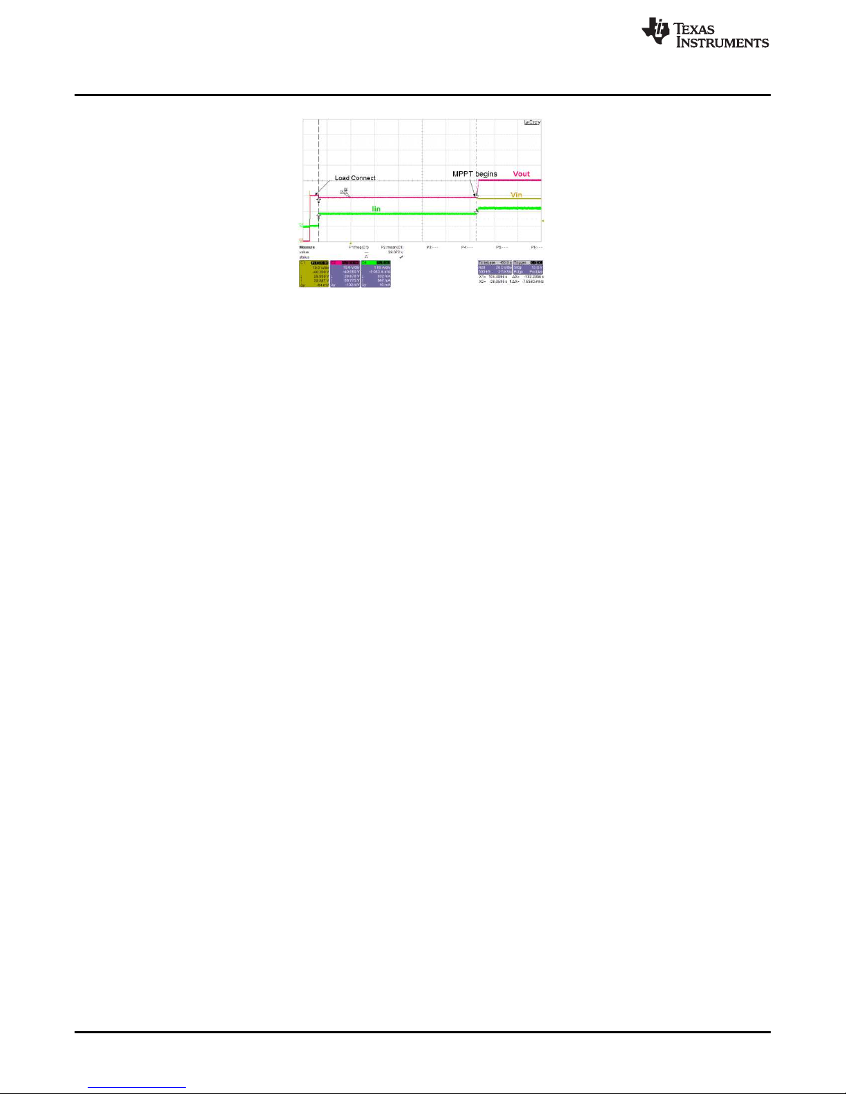
5 Load Connect and Stand-By Sequence After Start-Up................................................................ 8
6 Circuit Schematic ........................................................................................................... 9
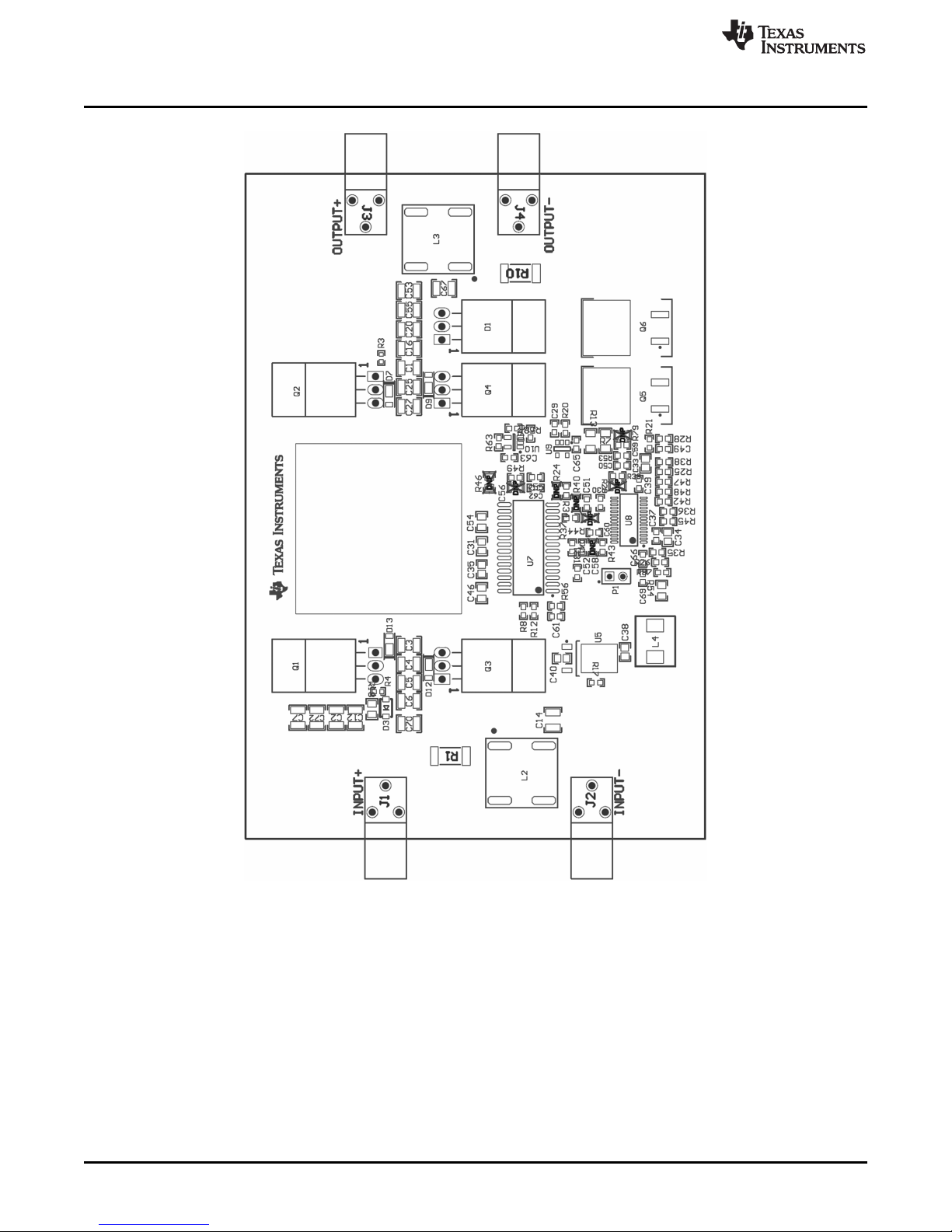
7 Top Assembly Diagram................................................................................................... 10
8 Bottom Assembly Diagram............................................................................................... 11
List of Figures
waveform was taken at drain of Q4.)..................................................................................... 6
All trademarks are the property of their respective owners.
SNVA649–May 2012 List of Figures
Submit Documentation Feedback
3
Copyright © 2012, Texas Instruments Incorporated
Page 4

User's Guide
SNVA649–May 2012
AN-2241 SM72445 Evaluation Board
The SolarMagic™ SM72445 Evaluation Board is designed to demonstrate the operation and the
capabilities of the SM72445 MPPT controller. The board consists of a high efficiency, four-switch BuckBoost DC/DC converter and a bidirectional FET based switch designed to bypass the DC/DC converter for
cases when DC/DC conversion is not needed and during failure of the DC/DC converter (over-current
protection, over-temperature, and so forth). The board also includes auxiliary circuits such as driver,
current sensor, temperature sensor and additional OVP circuitry.
4
AN-2241 SM72445 Evaluation Board SNVA649–May 2012
Copyright © 2012, Texas Instruments Incorporated
Submit Documentation Feedback
Page 5
DC/DC converter
Panel Mode
Bi-directional switch
SM72445
SM72295
Curr.
Sense amp.
Comparator
Temp. sensor
PV
Panel
LOAD
PWM signal
Gate Drive
Current
sense
Input
Current
sense
Input voltage
sense
Output voltage
sense
Protection trigger
Out current sense
Protection
trigger
www.ti.com
1 Introduction
The SM72445 is designed to maximize the energy production of a photovoltaic panel through the control
of a four switch buck-boost converter as well as an optional FET bi-directional switch (two FETs) designed
to maximize the efficiency at 1:1 conversion ratios. The maximum voltage and power transferred depend
on the component choice (driver, passive components, FET, and so forth). The SM72445 performs
optimization of the operating point of the solar panel through a high speed Perturb&Observe algorithm.
The input voltage and current are sampled at a high rate and digitally filtered while the algorithm updates
the output PWM waveform at a rate up to 1.2ms/step. The PWM waveforms include dead-time and can be
directly fed to the drivers controlling the DC/DC converter’s switches. The SM72445 is designed to
operate at 110kHz, 137kHz and 220kHz depending on the operating mode set. The SM72445 includes
and I2C slave module with 8 address settings to communicate monitoring information and to allow remote
shut-down and configuration modifications.
The SolarMagic™ SM72445 Evaluation Board is based off of the SM3320-1A1 power optimizer, and
shares all of its best-in-class power optimization features. This includes its ability to mitigate real-world
mismatch, its 99.5% peak efficiency, and its Panel-Mode operation. In addition, the same ultra-low profile
form factor of the original SM3320-1A1 is maintained so that it can be integrated into the same junction
box designs.
This Evaluation module is fully operational and can be used with panels from 15V up to 50V (absolute)
operating voltage and up to 300W of power. Proper heat-sinking of the Power FETs must be achieved for
power levels above 50W at room temperature.
The absolute maximum output voltage is 50V. The maximum operating current is 11A
Introduction
2 System Overview
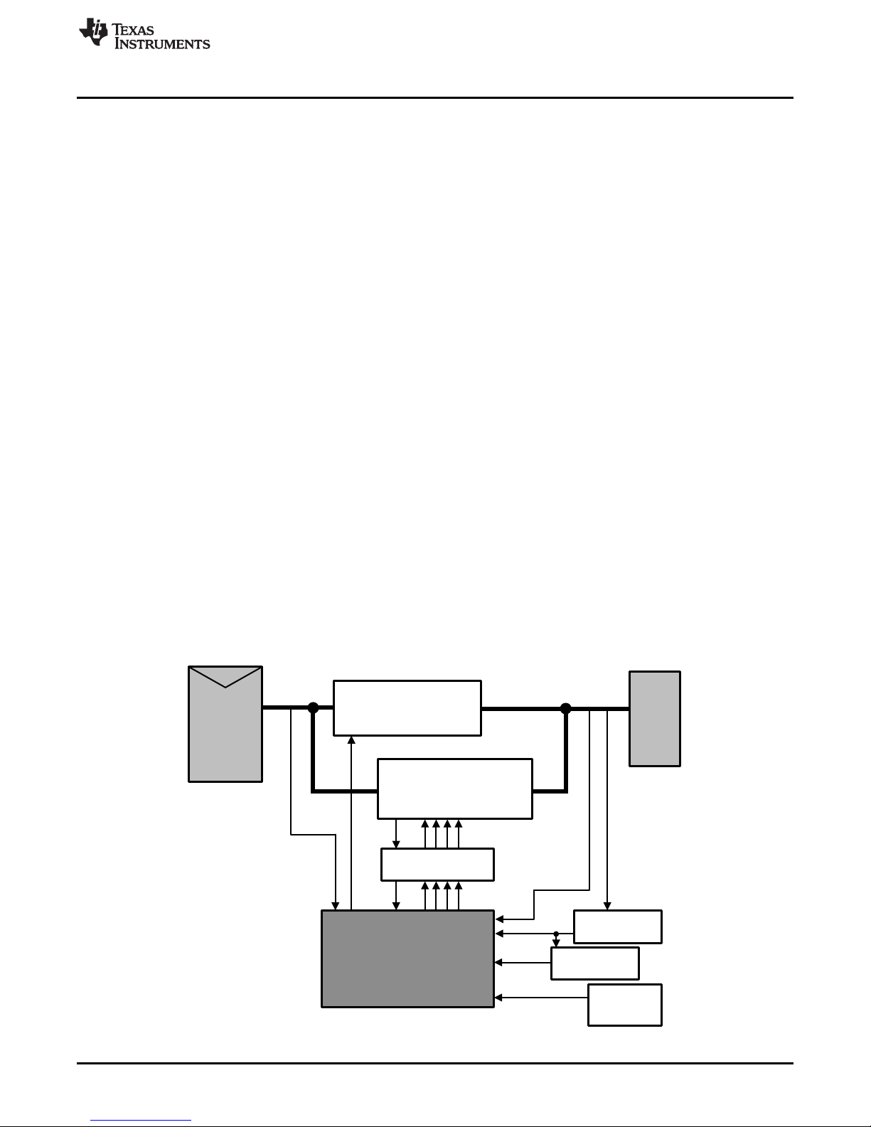
Figure 1 depicts how the SM72445 design would be implemented in its intended application. In this
example, the SM72445 senses the input and output voltages and currents, filters them digitally and
calculates power. It then issues four PWM pulses to the gate drivers to control the converter's switches.
The SM72445 also operates an additional switch (called Panel-Mode or PM switch) to optimize efficiency
when operating close to a 1:1 conversion ratio. Optionally, the switch can be omitted for reduced cost. The
SM72445 then utilizes the converter at a 1:1 conversion ratio and increases efficiency by reducing the
switching frequency of the converter
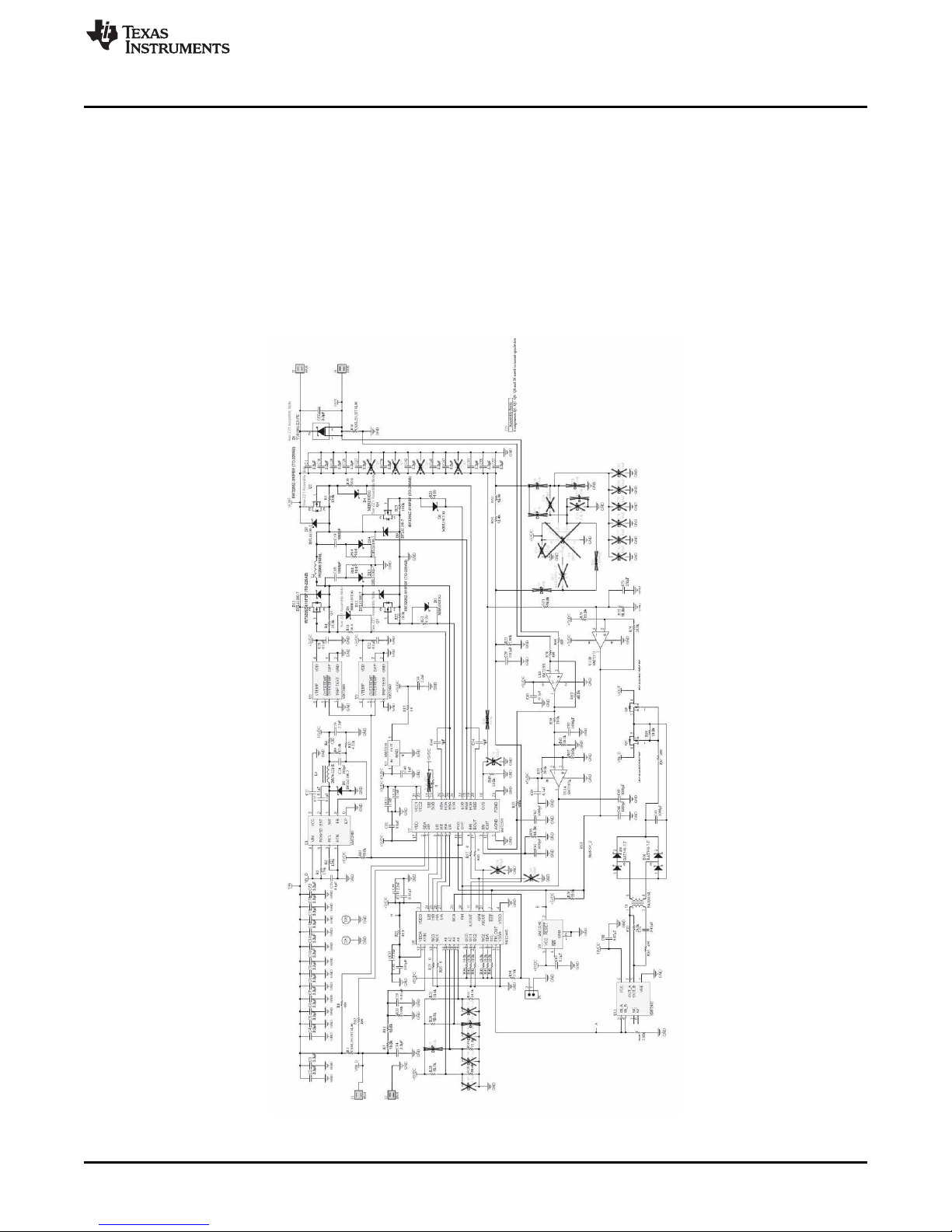
Figure 6 shows the detailed schematic with component references.
Figure 1. Evaluation Board Simplified Diagram
SNVA649–May 2012 AN-2241 SM72445 Evaluation Board
Submit Documentation Feedback
Copyright © 2012, Texas Instruments Incorporated
5
Page 6

Buck
Boost
SM72445 Evaluation module Design Specification
3 SM72445 Evaluation module
Design Specification
Symbol Parameter Min Typ Max
V
MPP
P
MPP
V
OC
I
SC
V
OUT
I
OUT
OVP Overvoltage Protection Threshold 45V
OTP Overtemperature Protection Threshold 125oC
MPP
EFF
PM
EFF
CONFIGURATION MODES
The SM72445 is configured through I2C communication or through resistor settings on pin A0, A2, A4 and
A6. The default configuration setting on the board is:
Pin name Pin Voltage Description
A0 3.0V “Soft” output voltage limit of 40V (AVOUT=3V)
A2 0V 220kHz operation, uses dedicated FET switch for higher efficiency
A4 5.0V Internal current protection not used
A6 1.56V Long slew rate limit, 60s in a 1:1 conversion ratio at start-up before enabling
PV Module MPP Voltage 15 Vdc 40Vdc
PV Module Power 10 W 350 W
PV Module Open Circuit Voltage 50 Vdc
PV Module Short-Circuit Current 11A
Output Voltage 0 Vdc 43 Vdc
Output Current 12.5A
MPP Efficiency 98.5%
Panel-Mode Efficiency 99.5%
www.ti.com
optimization
Modifications to the configuration can be performed by changing the resistor settings. The change in
configuration will only happen at start-up and during reset of the IC.
“PANEL MODE” OPERATION
The board is configured to use “Panel Mode” FETs to reach the highest possible efficiency at a 1:1
conversion ratio. The SM72445 will disconnect the DC/DC converter and turn on this switch whenever it
detects that the panel is matched to the load. The detail of this operation can be found in the SM72445
datasheet. Alternatively, the SM72445 can be configured to run the DC/DC converter in a Panel-Mode
behavior instead, driving the high-side FETs of the converter in a mostly ONstate (Figure 2) and achieving
the same function as the dedicated Panel-Mode FETs. This option optimizes the component count and the
cost of the solution but slightly reduces the efficiency of the system in the band close to a 1:1 conversion
ratio. To configure the board in this mode, the resistor couple R29 and R39 can be changed to modify the
voltage at pin A2. In addition, T1 should be removed. Check the SM72445 datasheet for additional details
on the different configuration settings.
Figure 2. Panel Mode Operation Using Converter's FET (“Boost” waveform is taken at drain of Q3,
“Buck” waveform was taken at drain of Q4.)
6
AN-2241 SM72445 Evaluation Board SNVA649–May 2012
Copyright © 2012, Texas Instruments Incorporated
Submit Documentation Feedback
Page 7

www.ti.com
“SOFT” OUTPUT VOLTAGE LIMIT
The soft output voltage limit of “Soft OVP” is designed to prevent the output voltage from reaching
dangerous level when the system is running the converter in boost mode. This mechanism works by
reducing the duty cycle of the converter when the voltage at pin AVOUT is increasing above the voltage at
pin A0.
SLEW RATE LIMIT
The slew rate limit is designed to limit the rate of rise of the output voltage when and only when the
converter is running in boost mode. The rise of the duty cycle will be limited to ensure that the output
voltage will rise in a controlled manner, especially during transients such as when the load is reduced or
gets removed (before the SM72445 returns in stand-by mode). To test the slew rate limit, start-up the
system with a current load at 1.5A and with an input that has a maximum power point above 3A. The
output voltage will increase very rapidly until it reaches the input voltage. The output voltage will then
increase slowly above the input voltage as limited by the slew rate setting programmed.
SM72445 Evaluation module Design Specification
Figure 3. Slew Rate Limit (between the two markers) and Soft OVP (after the second marker)
STARTUP
When starting up at no load, the SM72445 will increase the duty cycle until a 1:1 conversion ratio is
reached. The system will then enter a stand-by mode and wait for the detection of power by sensing the
output current. When the voltage on AIOUT rises above the internal threshold, the system will wait for a
typical period of 64 seconds and exit the stand-by mode. This is to allow the proper start-up of a potential
inverter connected to the string of panels in which the SM72445 based optimizer would be inserted. Upon
exiting stand-by mode, the system will enter “PM mode” (see SM72445 datasheet for further explanation).
MPPT will be enabled if power variation is detected. If no power variation is detected such as when the
system is connected to a DC Electronic load for example, MPPT will be enabled only after the “PM mode”
timer expires after an additional period of 64 seconds.
Figure 4. Start-Up Pattern With Unloaded Output
SNVA649–May 2012 AN-2241 SM72445 Evaluation Board
Submit Documentation Feedback
7
Copyright © 2012, Texas Instruments Incorporated
Page 8
SM72445 Evaluation module Design Specification
Figure 5. Load Connect and Stand-By Sequence After Start-Up
When a load is already present on the output of the board, the SM72445 will increase the duty cycle and
immediately enable MPPT operation when the voltages on AIOUT and AIIN rise above the internal
threshold.
INTERNAL CURRENT PROTECTION
If the voltage at AIOUT rises above the value set in A4, the system will reset. If AIOUT is set at or above
VDDA, this feature will be de-activated. The default setting for this board has this feature de-activated.
Current protection is performed using an external comparator
BOARD CURRENT PROTECTION
The board features a current protection circuit with U11A activating the PM pin of the SM72445 and
forcing the PM mode bypass switch to turn on (or the bridge to switch to 1:1 operation if the board is
reconfigured) when the output current reaches 13.5A. The output current will then be limited by the input
(solar panel) current. It is important to verify that the maximum solar panel current does not exceed the
rating of the components.
TEMPERATURE PROTECTION
U2 and U3 are strategically placed near the highest source of heat in the system (Q1 and Q4). When the
temperature reaches the tripping point (120 C), the ICs will activate the PM mode of the SM72445 by
forcing the PM pin low.
OVER-VOLTAGE PROTECTION
U11B forces the SM72445 to reset if the output voltage rises above 44V.
PANEL MODE SWITCH
Q5 and Q6 form a bi-directional switch controlled by the SM72445 and driven by U13 through T1. The
SM72445 supplies a 440kHz square waveform to turn on the switch.
GATE DRIVER
U7 is a quad 3A gate driver (two high and two low). It contains high-side operational amplifiers and buffers
used to sense the input current for MPPT purposes.
HEATSINKING
SM72445 evaluation board does not come with a heatsink. Therefore, in order to run the evaluation board
at elevated power ratings, an appropriate heatsink should be added on Q1, Q2, Q3 and Q4 as well as
diode D1. Care must be taken to prevent electrical contact between the drains of the MOSFETs in the
process of proper heatsinking. At elevated power operation please note the increase in temperature
across these semiconductor devices.
TEST SETUP
To perform an evaluation on the SM72445 evaluation board, it is suggested that the user connect the
input to a SAS (Solar Array Simulator) and the output to a load bank, preferably in Current mode (Voltage
mode sometimes causes regulation issues with some electronic load when used with the evaluation
board). The following sequence can be used to verify the operation of the board:
www.ti.com
8
AN-2241 SM72445 Evaluation Board SNVA649–May 2012
Copyright © 2012, Texas Instruments Incorporated
Submit Documentation Feedback
Page 9
www.ti.com
• Connect S.A.S. to input.
• Connect Electronic load to output.
• Turn on SAS Verify proper startup pattern (see Figure 4).
• Set Electronic load to 2A and turn on Electronic load.
• Wait two minutes and verify that SAS is operating at Maximum Power Point. If output voltage is
close to 40V, increase Electronic load current.
• Vary Electronic load current and verify that the SAS is operating at Maximum Power Point in
step-up (lower load current) and step-down (higher load current) operation.
4 Schematic
Schematic
SNVA649–May 2012 AN-2241 SM72445 Evaluation Board
Submit Documentation Feedback
Figure 6. Circuit Schematic
9
Copyright © 2012, Texas Instruments Incorporated
Page 10
Schematic
www.ti.com
10
AN-2241 SM72445 Evaluation Board SNVA649–May 2012
Figure 7. Top Assembly Diagram
Copyright © 2012, Texas Instruments Incorporated
Submit Documentation Feedback
Page 11

www.ti.com
Bill of Material
5 Bill of Material
SNVA649–May 2012 AN-2241 SM72445 Evaluation Board
Submit Documentation Feedback
Figure 8. Bottom Assembly Diagram
11
Copyright © 2012, Texas Instruments Incorporated
Page 12

Bill of Material
www.ti.com
Table 1. Bill of Material
Designator Part Description Qty. Manufacturer Part number
C1, C2, C3, C4, CAP, CERM, 3.3µF, 50V, ±20%, X7R, 1210 28 TDK C3225X7R1H335M
C5, C6, C7, C8,
C9, C10, C11,
C12, C13, C14,
C16, C20, C25,
C27, C30, C42,
C45, C47, C53,
C55, C57, C67,
C70, C72
C15, C17, C22, CAP, CERM, 0.1µF, 16V, ±10%, X7R, 0603 8 Taiyo Yuden EMK107B7104KA-T
C26, C32, C63,
C64, C65
C18, C19 CAP, CERM, 1000pF, 100V, ±10%, X7R, 0805 2 Kemet C0805C102K1RACTU
C21 CAP, CERM, 0.1µF, 100V, ±10%, X7R, 0805 1 Kemet C0805C104K1RACTU
C23, C33, C34, CAP, CERM, 2.2µF, 16V, ±10%, X7R, 0805 4 Taiyo Yuden EMK212B7225KG-T
C38
C24 CAP, CERM, 330pF, 50V, ±10%, X7R, 0603 1 Kemet C0603C331K5RACTU
C29, C37, C39, CAP, CERM, 0.01µF, 50V, ±10%, X7R, 0603 4 Kemet C0603C103K5RACTU
C59
C31, C35, C40, CAP, CERM, 1µF, 16V, ±10%, X7R, 0805 5 Taiyo Yuden EMK212B7105KG-T
C46, C54
C43, C61, C62, CAP, CERM, 1000pF, 50V, ±10%, X7R, 0603 6 Kemet C0603C102K5RACTU
C66, C69, C82
C68, C71 CAP, CERM, 0.47µF, 16V, ±10%, X7R, 0805 2 TDK C2012X7R1C474K
C73 CAP, CERM, 150pF, 50V, ±5%, C0G/NP0, 0603 1 Kemet C0603C151J5GACTU
D1 DIODE SCHOTTKY 30A 100V TO-220AB 1 Vishay-Semiconductor V30100S-E3/4W
D2, D7, D9, D12, Diode, Schottky, 100V, 1A, PowerDI123 7 Diodes Inc. DFLS1100-7
D13, D14, D15
D3, D4, D5, D6 Diode, Schottky, 30V, 1A, SOD-123 4 ON Semiconductor MBR130T1G
D8, D10 Diode, Schottky, 30V, 0.2A, SOT-23 2 Diodes Inc. BAT54S-7-F
J1, J2, J3, J4 PC Quick-Fit 0.250 Horizontal Tab 4 Keystone Electronics 4910
L1 Inductor 20 µH EFD-30 core 1 Pulse Electronics PA2965.203NL
L2, L3 Choke, Filter 2 Pulse PA2972NL
L4 Inductor, Shielded Drum Core, Ferrite, 220 µH, 1 Coiltronics DR74-221-R
P1 Header, TH, 100mil, 1x2, Tin plated, 230 mil 1 Samtec Inc. TSW-102-07-T-S
Q1, Q2, Q3, Q4 MOSFET 55V, 6.5m Ω 4 International Rectifier IRF3205Z-010PBF
Q5, Q6 MOSFET 60V, 2.4m Ω 2 International Rectifier IRFS3206TRRPBF
R1, R10 RES .004 Ω 2W 1% 2512 SMD 2 Stackpole Electronics Inc CSNL2512FT4L00
R2, R54 RES, 174k Ω, 1%, 0.125W, 0805 2 Vishay-Dale CRCW0805174KFKEA
R3, R4, R22, R23, RES, 10.0k Ω, 1%, 0.1W, 0603 13 Vishay-Dale CRCW060310k0FKEA
R36, R42, R43,
R45, R47, R48,
R49, R64, R72
R5 RES, 124k Ω, 1%, 0.1W, 0603 1 Vishay-Dale CRCW0603124kFKEA
R6 RES, 1.00 Ω, 1%, 0.125W, 0805 1 Vishay-Dale CRCW08051R00FNEA
R7, R13 RES, 10.0k Ω, 1%, 0.25W, 1206 2 Vishay-Dale CRCW120610K0FKEA
R8, R12, R16, RES, 499 Ω, 1%, 0.1W, 0603 6 Vishay-Dale CRCW0603499RFKEA
R58, R60, R67
R9 RES, 12.4k Ω, 1%, 0.1W, 0603 1 Vishay-Dale CRCW060312k4FKEA
R11, R14 RES, 10.0 Ω, 1%, 1W, 1218 SMD 2 Vishay-Dale CRCW121810R0FKEK
R15 RES, 4.22k Ω, 1%, 0.1W, 0603 1 Vishay-Dale CRCW06034k22FKEA
R17 RES, 1.0 Ω, 1%, 0.1W, 0603 1 Panasonic ERJ3RQF1R0V
0.56A, 0.907 Ω, SMD
above insulator
12
AN-2241 SM72445 Evaluation Board SNVA649–May 2012
Copyright © 2012, Texas Instruments Incorporated
Submit Documentation Feedback
Page 13

www.ti.com
Bill of Material
Table 1. Bill of Material (continued)
Designator Part Description Qty. Manufacturer Part number
R18, R19 RES, 10.0 Ω, 1%, 0.125W, 0805 2 Vishay-Dale CRCW080510R0FKEA
R20, R53, R69 RES, 2.00k Ω, 1%, 0.1W, 0603 3 Vishay-Dale CRCW06032k00FKEA
R21 RES, 49.9 Ω, 1%, 0.1W, 0603 1 Vishay-Dale CRCW060349R9FKEA
R25, R34, R35, RES, 0 Ω, 5%, 0.1W, 0603 5 Vishay-Dale CRCW06030000Z0EA
R37, R44
R26, R87 RES, 59.0k Ω, 1%, 0.1W, 0603 2 Vishay-Dale CRCW060359K0FKEA
R28, R30 RES, 19.1k Ω, 1%, 0.1W, 0603 2 Vishay-Dale CRCW060319K1FKEA
R31 RES, 31.6k Ω, 1%, 0.1W, 0603 1 Vishay-Dale CRCW060331K6FKEA
R32, R33 RES, 4.99 Ω, 1%, 0.125W, 0805 2 Vishay-Dale CRCW08054R99FNEA
R38 RES, 29.4k Ω, 1%, 0.1W, 0603 1 Vishay-Dale CRCW060329K4FKEA
R39 RES, 15.8k Ω, 1%, 0.1W, 0603 1 Vishay-Dale CRCW060315K8FKEA
R41 RES, 14.3k Ω, 1%, 0.1W, 0603 1 Vishay-Dale CRCW060314K3FKEA
R51, R52 RES, 12.4k Ω, 1%, 0.25W, 1206 2 Vishay-Dale CRCW120612K4FKEA
R55 RES, 100k Ω, 1%, 0.1W, 0603 1 Vishay-Dale CRCW0603100KFKEA
R56 RES, 45.3k Ω, 1%, 0.1W, 0603 1 Vishay-Dale CRCW060345K3FKEA
R57, R59, R62, RES, 20.0k Ω, 1%, 0.1W, 0603 5 Vishay-Dale CRCW060320K0FKEA
R70, R74
R61 RES, 26.1k Ω, 1%, 0.1W, 0603 1 Vishay-Dale CRCW060326K1FKEA
R63 RES, 40.2k Ω, 1%, 0.1W, 0603 1 Vishay-Dale CRCW060340K2FKEA
R71 RES, 76.8k Ω, 1%, 0.125W, 0805 1 Vishay-Dale CRCW080576K8FKEA
R73 RES, 23.2k Ω, 1%, 0.1W, 0603 1 Vishay-Dale CRCW060323K2FKEA
T1 SMT GATE TRANS 1:1 1500V 403 uH 0.60R 1 Pulse Electronics PA2001NL
TP1, TP2 Test Point, SMT, Miniature 2 Keystone Electronics 5015
U1 100V, 150 mA Constant On-Time Buck Switching 1 National Semiconductor SM72485
U2, U3 1.6V, LLP-6 Factory Preset Temperature Switch 2 National Semiconductor SM72480
U5 5V Micropower Voltage Regulator 1 National Semiconductor SM72238
U7 Photovoltaic Full Bridge Driver 1 National Semiconductor SM72295
U8 Programmable Maximum Power Point Tracking 1 Texas Instruments SM72445
U9 5-Pin Microprocessor Reset Circuits 1 National Semiconductor SM72240
U10 Precision, CMOS Input, RRIO, Wide Supply 1 National Semiconductor SM72501
U11 Dual Micropower Rail-To-Rail Input CMOS 1 National Semiconductor SM72375
U13 Dual 5A Compound Gate Driver 1 National Semiconductor SM72482
Regulator
and Temperature Sensor
Controller With Adjustable PWM Frequency
Range Amplifier
Comparator with Open Drain Output
SNVA649–May 2012 AN-2241 SM72445 Evaluation Board
Submit Documentation Feedback
13
Copyright © 2012, Texas Instruments Incorporated
Page 14

IMPORTANT NOTICE
Texas Instruments Incorporated and its subsidiaries (TI) reserve the right to make corrections, enhancements, improvements and other
changes to its semiconductor products and services per JESD46, latest issue, and to discontinue any product or service per JESD48, latest
issue. Buyers should obtain the latest relevant information before placing orders and should verify that such information is current and
complete. All semiconductor products (also referred to herein as “components”) are sold subject to TI’s terms and conditions of sale
supplied at the time of order acknowledgment.
TI warrants performance of its components to the specifications applicable at the time of sale, in accordance with the warranty in TI’s terms
and conditions of sale of semiconductor products. Testing and other quality control techniques are used to the extent TI deems necessary
to support this warranty. Except where mandated by applicable law, testing of all parameters of each component is not necessarily
performed.
TI assumes no liability for applications assistance or the design of Buyers’ products. Buyers are responsible for their products and
applications using TI components. To minimize the risks associated with Buyers’ products and applications, Buyers should provide
adequate design and operating safeguards.
TI does not warrant or represent that any license, either express or implied, is granted under any patent right, copyright, mask work right, or
other intellectual property right relating to any combination, machine, or process in which TI components or services are used. Information
published by TI regarding third-party products or services does not constitute a license to use such products or services or a warranty or
endorsement thereof. Use of such information may require a license from a third party under the patents or other intellectual property of the
third party, or a license from TI under the patents or other intellectual property of TI.
Reproduction of significant portions of TI information in TI data books or data sheets is permissible only if reproduction is without alteration
and is accompanied by all associated warranties, conditions, limitations, and notices. TI is not responsible or liable for such altered
documentation. Information of third parties may be subject to additional restrictions.
Resale of TI components or services with statements different from or beyond the parameters stated by TI for that component or service
voids all express and any implied warranties for the associated TI component or service and is an unfair and deceptive business practice.
TI is not responsible or liable for any such statements.
Buyer acknowledges and agrees that it is solely responsible for compliance with all legal, regulatory and safety-related requirements
concerning its products, and any use of TI components in its applications, notwithstanding any applications-related information or support
that may be provided by TI. Buyer represents and agrees that it has all the necessary expertise to create and implement safeguards which
anticipate dangerous consequences of failures, monitor failures and their consequences, lessen the likelihood of failures that might cause
harm and take appropriate remedial actions. Buyer will fully indemnify TI and its representatives against any damages arising out of the use
of any TI components in safety-critical applications.
In some cases, TI components may be promoted specifically to facilitate safety-related applications. With such components, TI’s goal is to
help enable customers to design and create their own end-product solutions that meet applicable functional safety standards and
requirements. Nonetheless, such components are subject to these terms.
No TI components are authorized for use in FDA Class III (or similar life-critical medical equipment) unless authorized officers of the parties
have executed a special agreement specifically governing such use.
Only those TI components which TI has specifically designated as military grade or “enhanced plastic” are designed and intended for use in
military/aerospace applications or environments. Buyer acknowledges and agrees that any military or aerospace use of TI components
which have not been so designated is solely at the Buyer's risk, and that Buyer is solely responsible for compliance with all legal and
regulatory requirements in connection with such use.
TI has specifically designated certain components as meeting ISO/TS16949 requirements, mainly for automotive use. In any case of use of
non-designated products, TI will not be responsible for any failure to meet ISO/TS16949.
Products Applications
Audio www.ti.com/audio Automotive and Transportation www.ti.com/automotive
Amplifiers amplifier.ti.com Communications and Telecom www.ti.com/communications
Data Converters dataconverter.ti.com Computers and Peripherals www.ti.com/computers
DLP® Products www.dlp.com Consumer Electronics www.ti.com/consumer-apps
DSP dsp.ti.com Energy and Lighting www.ti.com/energy
Clocks and Timers www.ti.com/clocks Industrial www.ti.com/industrial
Interface interface.ti.com Medical www.ti.com/medical
Logic logic.ti.com Security www.ti.com/security
Power Mgmt power.ti.com Space, Avionics and Defense www.ti.com/space-avionics-defense
Microcontrollers microcontroller.ti.com Video and Imaging www.ti.com/video
RFID www.ti-rfid.com
OMAP Applications Processors www.ti.com/omap TI E2E Community e2e.ti.com
Wireless Connectivity www.ti.com/wirelessconnectivity
Mailing Address: Texas Instruments, Post Office Box 655303, Dallas, Texas 75265
Copyright © 2012, Texas Instruments Incorporated
Page 15

Mouser Electronics
Authorized Distributor
Click to View Pricing, Inventory, Delivery & Lifecycle Information:
Texas Instruments:
SM72445EVM/NOPB
 Loading...