Texas Instruments ADS8674, ADS8678 Datasheet
-0.05
-0.03
-0.01
0.01
0.03
0.05
±40 ±7
26 59 92 125
Gain (% FS)
Free-Air Temperature (oC)
C039
---- ± 2.5*V
REF,
---- 1.25*V
REF
---- 0.625*V
REF,
------0.3125*V
REF
-------0.156 V
REF,
---- + 2.5*V
REF
---- + 1.25*V
REF,
---- + 0.625*V
REF
---- + 0.3125*V
REF
Multiplexer
Oscillator
CS
SCLK
SDI
SDO
DAISY
REFSEL
RST/PD
REFCAP
REFIO
PGA
1 M:
OVP
1 M:
2nd-Order
LPF
ADC
Driver
V
B0
AIN_0P
AIN_0GND
OVP
PGA
1 M:
OVP
1 M:
2nd-Order
LPF
ADC
Driver
V
B1
AIN_1P
AIN_1GND
OVP
PGA
1 M:
OVP
1 M:
2nd-Order
LPF
ADC
Driver
V
B2
AIN_2P
AIN_2GND
OVP
PGA
1 M:
OVP
1 M:
2nd-Order
LPF
ADC
Driver
V
B3
AIN_3P
AIN_3GND
OVP
PGA
1 M:
OVP
1 M:
2nd-Order
LPF
ADC
Driver
V
B4
AIN_4P
AIN_4GND
OVP
PGA
1 M:
OVP
1 M:
2nd-Order
LPF
ADC
Driver
V
B5
AIN_5P
AIN_5GND
OVP
PGA
1 M:
OVP
1 M:
2nd-Order
LPF
ADC
Driver
V
B6
AIN_6P
AIN_6GND
OVP
PGA
1 M:
OVP
1 M:
2nd-Order
LPF
ADC
Driver
V
B7
AIN_7P
AIN_7GND
OVP
AUX_IN
AUX_GND
14-Bit
SAR ADC
Digital
Logic
and
Interface
4.096-V
Reference
REFGND
DGNDAGND
DVDD
AVDD
Additional Channels in ADS8678
ADS8678
ADS8674
ALARM
Product
Folder
Sample &
Buy
Technical
Documents
Tools &
Software
Support &
Community
Reference
Design
ADS867x 14-Bit, 500-kSPS, 4- and 8-Channel, Single-Supply, SAR ADCs with
Bipolar Input Ranges
1 Features 2 Applications
1
• 14-Bit ADCs with Integrated Analog Front-End
• 4-, 8-Channel MUX with Auto and Manual Scan • Protection Relays
• Channel-Independent Programmable Inputs: • PLC Analog Input Modules
– ±10.24 V, ±5.12 V, ±2.56 V, ±1.28 V, ±0.64 V
– 10.24 V, 5.12 V, 2.56 V, 1.28 V
• 5-V Analog Supply: 1.65-V to 5-V I/O Supply
• Constant Resistive Input Impedance: 1 MΩ
• Input Overvoltage Protection: Up to ±20 V
• On-Chip, 4.096-V Reference with Low Drift
• Excellent Performance:
– 500-kSPS Aggregate Throughput
– DNL: ±0.2 LSB; INL: ±0.25 LSB
– Low Drift for Gain Error and Offset
– SNR: 85 dB; THD: –100 dB
– Low Power: 65 mW
• AUX Input → Direct Connection to ADC Inputs
• ALARM → High and Low Thresholds per Channel
• SPI™-Compatible Interface with Daisy-Chain
• Industrial Temperature Range: –40°C to 125°C
• TSSOP-38 Package (9.7 mm × 4.4 mm)
Block Diagram
• Power Automation
3 Description
The ADS8674 and ADS8678 are 4- and 8-channel,
integrated data acquisition systems based on a 14-bit
successive approximation (SAR) analog-to-digital
converter (ADC), operating at a throughput of
500 kSPS. The devices feature integrated analog
front-end circuitry for each input channel with
overvoltage protection up to ±20 V, a 4- or 8-channel
multiplexer with automatic and manual scanning
modes, and an on-chip, 4.096-V reference with low
temperature drift. Operating on a single 5-V analog
supply, each input channel on the devices can
support true bipolar input ranges of ±10.24 V,
±5.12 V, ±2.56 V, ±1.28V and ±0.64V, as well as
unipolar input ranges of 0 V to 10.24 V, 0 V to 5.12 V,
0 V to 2.56 V and 0 V to 1.28 V. The gain of the
analog front-end for all input ranges is accurately
trimmed to ensure a high dc precision. The input
range selection is software-programmable and
independent for each channel. The devices offer a
1-MΩ constant resistive input impedance irrespective
of the selected input range.
The ADS8674 and ADS8678 offer a simple SPIcompatible serial interface to the digital host and also
support daisy-chaining of multiple devices. The digital
supply operates from 1.65 V to 5.25 V, enabling
direct interface to a wide range of host controllers.
ADS8674,ADS8678
SBAS627 –JULY 2015
1
Device Information
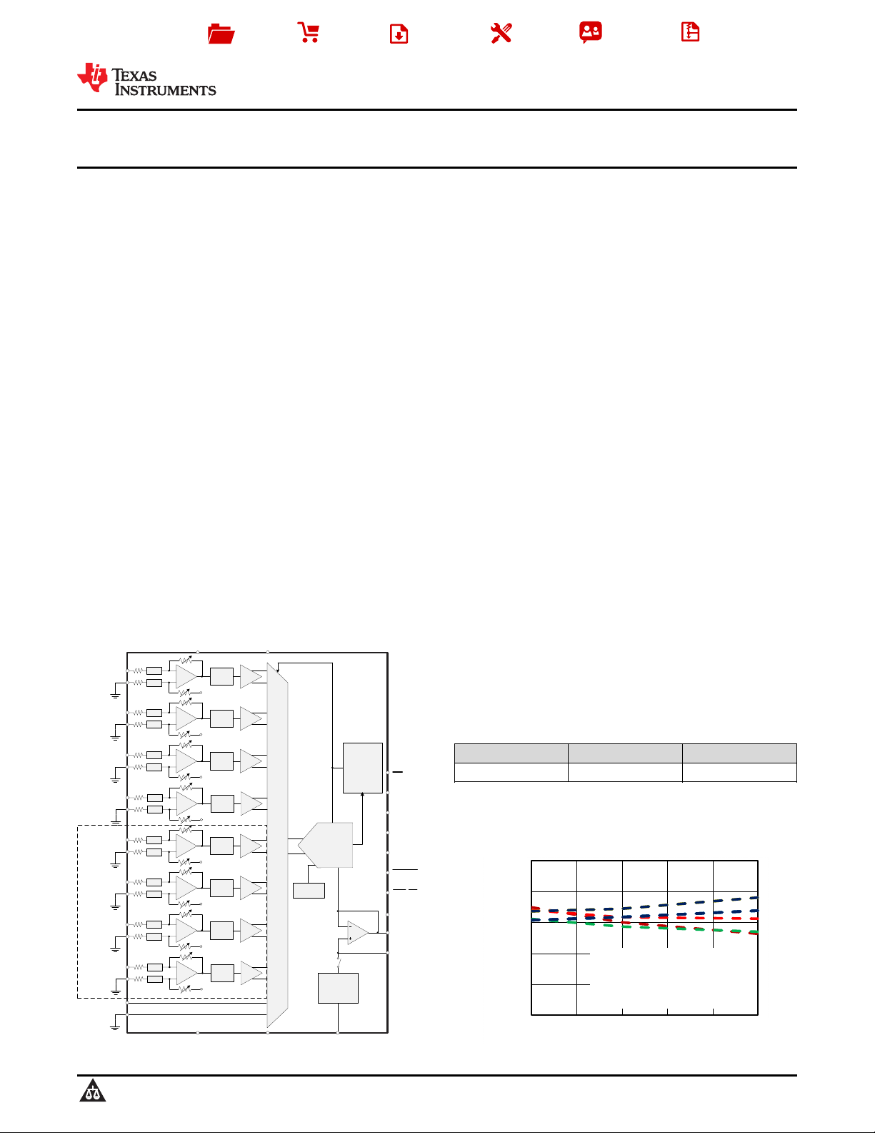
Gain Error versus Temperature
PART NUMBER PACKAGE BODY SIZE (NOM)
ADS867x TSSOP (38) 9.70 mm × 4.40 mm
(1) For all available packages, see the orderable addendum at
the end of the datasheet.
An IMPORTANT NOTICE at the end of this data sheet addresses availability, warranty, changes, use in safety-critical applications,
intellectual property matters and other important disclaimers. PRODUCTION DATA.
(1)

ADS8674,ADS8678
SBAS627 –JULY 2015
www.ti.com
Table of Contents
1 Features.................................................................. 1
2 Applications ........................................................... 1
3 Description ............................................................. 1
4 Revision History..................................................... 2
5 Device Comparison Table..................................... 3
6 Pin Configuration and Functions......................... 3
7 Specifications......................................................... 5
7.1 Absolute Maximum Ratings ...................................... 5
7.2 ESD Ratings.............................................................. 5
7.3 Recommended Operating Conditions....................... 5
7.4 Thermal Information.................................................. 5
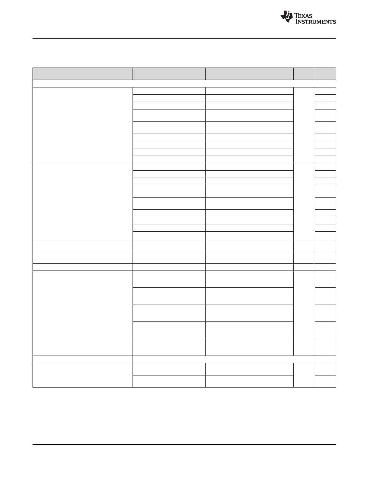
7.5 Electrical Characteristics........................................... 6
7.6 Timing Requirements: Serial Interface.................... 10
7.7 Typical Characteristics............................................ 11
8 Detailed Description ............................................ 22
8.1 Overview ................................................................. 22
8.2 Functional Block Diagram....................................... 22
8.3 Feature Description................................................. 23
4 Revision History
DATE REVISION NOTES
July 2014 * Initial release.
8.4 Device Functional Modes........................................ 36
8.5 Register Maps......................................................... 49
9 Application and Implementation........................ 65
9.1 Application Information............................................ 65
9.2 Typical Applications ................................................ 65
10 Power-Supply Recommendations ..................... 68
11 Layout................................................................... 69
11.1 Layout Guidelines ................................................. 69
11.2 Layout Example .................................................... 70
12 Device and Documentation Support................. 71
12.1 Documentation Support ........................................ 71
12.2 Related Links ........................................................ 71
12.3 Community Resources.......................................... 71
12.4 Trademarks........................................................... 71
12.5 Electrostatic Discharge Caution............................ 71
12.6 Glossary................................................................ 71
13 Mechanical, Packaging, and Orderable
Information........................................................... 72
2 Submit Documentation Feedback Copyright © 2015, Texas Instruments Incorporated
Product Folder Links: ADS8674 ADS8678
1
2
3
4
5
6
7
8
30
29
28
27
26
25
24
CS
SCLK
SDO
ALARM
DVDD
DGND
AGND
AGND
SDI
RST/PD
DAISY
REFSEL
REFIO
REFGND
REFCAP
22
21
20
AVDD
AGND
AGND
AIN_5P
AIN_5GND
AIN_4P
AIN_4GND
9AVDD
AUX_IN
AUX_GND
AIN_6P
AIN_6GND
AIN_7P
AIN_7GND
10
11
12
13
14
15
23
AIN_3P
AIN_3GND
AIN_2P
AIN2_GND
AIN_0P
AIN_0GND
AIN_1P
AIN_1GND
16
17
18
19
31
32
33
34
35
36
37
38
AGND
ADS8678
1
2
3
4
5
6
7
8
30
29
28
27
26
25
24
CS
SCLK
SDO
ALARM
DVDD
DGND
AGND
AGND
SDI
RST/PD
DAISY
REFSEL
REFIO
REFGND
REFCAP
22
21
20
AVDD
AGND
AGND
NC
NC
NC
NC
9AVDD
AUX_IN
AUX_GND
NC
NC
NC
NC
10
11
12
13
14
15
23
AIN_3P
AIN_3GND
AIN_2P
AIN2_GND
AIN_0P
AIN_0GND
AIN_1P
AIN_1GND
16
17
18
19
31
32
33
34
35
36
37
38
AGND
ADS8674
www.ti.com
5 Device Comparison Table
PRODUCT RESOLUTION (Bits) CHANNELS SAMPLE RATE (kSPS)
ADS8674 14 4, single-ended 500
ADS8678 14 8, single-ended 500
6 Pin Configuration and Functions
ADS8674,ADS8678
SBAS627 –JULY 2015
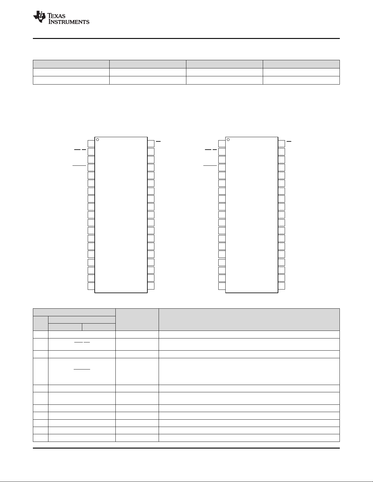
DBT Package
38-Pin TSSOP
Top View (Not to Scale)
Pin Functions
PIN
NO.
1 SDI Digital input Data input for serial communication.
2 RST/PD Digital input
3 DAISY Digital input Chain the data input during serial communication in daisy-chain mode.
4 REFSEL Digital input REFIO becomes an output that includes the V
5 REFIO Analog input, output Internal reference output and external reference input pin. Decouple with REFGND on pin 6.
6 REFGND Power supply
7 REFCAP Analog output ADC reference decoupling capacitor pin. Decouple with REFGND on pin 6.
8 AGND Power supply Analog ground pin. Decouple with AVDD on pin 9.
9 AVDD Power supply Analog supply pin. Decouple with AGND on pin 8.
10 AUX_IN Analog input Auxiliary input channel: positive input. Decouple with AUX_GND on pin 11.
11 AUX_GND Analog input Auxiliary input channel: negative input. Decouple with AUX_IN on pin 10.
Copyright © 2015, Texas Instruments Incorporated Submit Documentation Feedback 3
ADS8674 ADS8678
NAME I/O DESCRIPTION
Product Folder Links: ADS8674 ADS8678
Active low logic input.
Dual functionality to reset or power-down the device.
Active low logic input to enable the internal reference.
When low, the internal reference is enabled;
When high, the internal reference is disabled;
REFIO becomes an input to apply the external V
Reference GND pin; short to the analog GND plane.
Decouple with REFIO on pin 5 and REFCAP on pin 7.
REF
voltage.
REF
voltage.
ADS8674,ADS8678
SBAS627 –JULY 2015
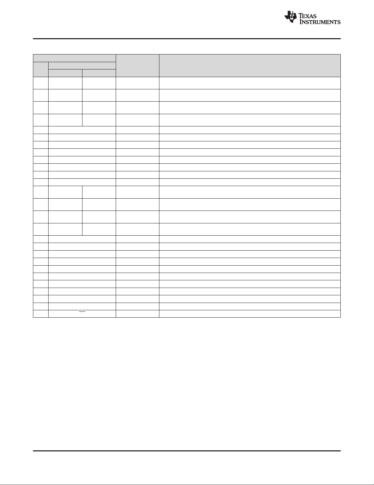
Pin Functions (continued)
PIN
NO.
12 NC AIN_6P Analog input
13 NC AIN_6GND Analog input
14 NC AIN_7P Analog input
15 NC AIN_7GND Analog input
16 AIN_0P Analog input Analog input channel 0, positive input. Decouple with AIN_0GND on pin 17.
17 AIN_0GND Analog input Analog input channel 0, negative input. Decouple with AIN_0P on pin 16.
18 AIN_1P Analog input Analog input channel 1, positive input. Decouple with AIN_1GND on pin 19.
19 AIN_1GND Analog input Analog input channel 1, negative input. Decouple with AIN_1P on pin 18.
20 AIN2_GND Analog input Analog input channel 2, negative input. Decouple with AIN_2P on pin 21.
21 AIN_2P Analog input Analog input channel 2, positive input. Decouple with AIN_2GND on pin 20.
22 AIN_3GND Analog input Analog input channel 3, negative input. Decouple with AIN_3P on pin 23.
23 AIN_3P Analog input Analog input channel 3, positive input. Decouple with AIN_3GND on pin 22.
24 NC AIN_4GND Analog input
25 NC AIN_4P Analog input
26 NC AIN_5GND Analog input
27 NC AIN_5P Analog input
28 AGND Power supply Analog ground pin
29 AGND Power supply Analog ground pin
30 AVDD Power supply Analog supply pin. Decouple with AGND on pin 31.
31 AGND Power supply Analog ground pin. Decouple with AVDD on pin 30.
32 AGND Power supply Analog ground pin
33 DGND Power supply Digital ground pin. Decouple with DVDD on pin 34.
34 DVDD Power supply Digital supply pin. Decouple with DGND on pin 33.
35 ALARM Digital output Active high alarm output
36 SDO Digital output Data output for serial communication
37 SCLK Digital input Clock input for serial communication
38 CS Digital input Active low logic input; chip-select signal
ADS8674 ADS8678
NAME I/O DESCRIPTION
Analog input channel 6, positive input. Decouple with AIN_6GND on pin 13.
No connection for the ADS8674; this pin can be left floating or connected to AGND.
Analog input channel 6, negative input. Decouple with AIN_6P on pin 12.
No connection for the ADS8674; this pin can be left floating or connected to AGND.
Analog input channel 7, positive input. Decouple with AIN_7GND on pin 15.
No connection for the ADS8674; this pin can be left floating or connected to AGND.
Analog input channel 7, negative input. Decouple with AIN_7P on pin 14.
No connection for the ADS8674; this pin can be left floating or connected to AGND.
Analog input channel 4, negative input. Decouple with AIN_4P on pin 25.
No connection for the ADS8674; this pin can be left floating or connected to AGND.
Analog input channel 4, positive input. Decouple with AIN_4GND on pin 24.
No connection for the ADS8674; this pin can be left floating or connected to AGND.
Analog input channel 5, negative input. Decouple with AIN_5P on pin 27.
No connection for the ADS8674; this pin can be left floating or connected to AGND.
Analog input channel 5, positive input. Decouple with AIN_5GND on pin 26.
No connection for the ADS8674; this pin can be left floating or connected to AGND.
www.ti.com
4 Submit Documentation Feedback Copyright © 2015, Texas Instruments Incorporated
Product Folder Links: ADS8674 ADS8678
ADS8674,ADS8678
www.ti.com
SBAS627 –JULY 2015
7 Specifications
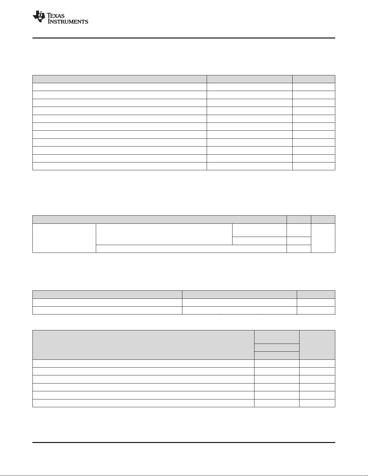
7.1 Absolute Maximum Ratings
over operating free-air temperature range (unless otherwise noted)
AIN_nP, AIN_nGND to GND
AIN_nP, AIN_nGND to GND
AUX_GND to GND –0.3 0.3 V
AUX_IN to GND –0.3 AVDD + 0.3 V
AVDD to GND or DVDD to GND –0.3 7 V
REFCAP to REFGND or REFIO to REFGND –0.3 5.7 V
GND to REFGND –0.3 0.3 V
Digital input pins to GND –0.3 DVDD + 0.3 V
Digital output pins to GND –0.3 DVDD + 0.3 V
Operating temperature, T
Storage temperature, T
(1) Stresses beyond those listed under Absolute Maximum Ratings may cause permanent damage to the device. These are stress ratings
only, and do not imply functional operation of the device at these or any other conditions beyond those indicated under Recommended
Operating Conditions. Exposure to absolute-maximum-rated conditions for extended periods may affect device reliability.
(2) AVDD = 5 V or offers a low impedance of < 30 kΩ.
(3) AVDD = floating with an impedance > 30 kΩ.
(2)
(3)
A
stg
(1)
MIN MAX UNIT
–20 20 V
–11 11 V
–40 125 °C
–65 150 °C
7.2 ESD Ratings
VALUE UNIT
V
Analog input pins
(1)
Electrostatic
(ESD)
discharge All other pins ±2000
Human body model (HBM), per ANSI/ESDA/JEDEC JS-001
Charged device model (CDM), per JEDEC specification JESD22-C101
(AIN_nP; AIN_nGND)
(2)
±4000
±500
(1) JEDEC document JEP155 states that 500-V HBM allows safe manufacturing with a standard ESD control process.
(2) JEDEC document JEP157 states that 250-V CDM allows safe manufacturing with a standard ESD control process.
7.3 Recommended Operating Conditions
over operating free-air temperature range (unless otherwise noted)
MIN NOM MAX UNIT
AVDD Analog supply voltage 4.75 5 5.25 V
DVDD Digital supply voltage 1.65 3.3 AVDD V
7.4 Thermal Information
ADS8674,
(1)
R
θJA
R
θJC(top)
R
θJB
ψ
JT
ψ
JB
R
θJC(bot)
THERMAL METRIC
Junction-to-ambient thermal resistance 68.8 °C/W
Junction-to-case (top) thermal resistance 19.9 °C/W
Junction-to-board thermal resistance 30.4 °C/W
Junction-to-top characterization parameter 1.3 °C/W
Junction-to-board characterization parameter 29.8 °C/W
Junction-to-case (bottom) thermal resistance NA °C/W
(1) For more information about traditional and new thermal metrics, see the IC Package Thermal Metrics application report, SPRA953.
ADS8678
DBT (TSSOP)
38 PINS
UNIT
V
Copyright © 2015, Texas Instruments Incorporated Submit Documentation Feedback 5
Product Folder Links: ADS8674 ADS8678
ADS8674,ADS8678
SBAS627 –JULY 2015
www.ti.com
7.5 Electrical Characteristics
Minimum and maximum specifications are at TA= –40°C to 125°C. Typical specifications are at TA= 25°C.
AVDD = 5 V, DVDD = 3 V, V
PARAMETER TEST CONDITIONS MIN TYP MAX UNIT
ANALOG INPUTS
Full-scale input span
(AIN_nP to AIN_nGND) Input range = ±0.15625 × V
AIN_nP –0.15625 × 0.15625 × V
AIN_nGND All input ranges –0.1 0 0.1 V B
z
i
I
Ikg(in)
INPUT OVERVOLTAGE PROTECTION
V
OVP
(1) Test Levels: (A) Tested at final test. Over temperature limits are set by characterization and simulation. (B) Limits set by characterization
and simulation, across temperature range. (C) Typical value only for information, provided by design simulation.
(2) Ideal input span, does not include gain or offset error.
Operating input range,
positive input Input range = ±0.15625 × V
Operating input range,
negative input
Input impedance 0.85 1 1.15 MΩ B
Input impedance drift All input ranges 7 25 ppm/°C B
Input leakage current input ranges = ±0.625 × V
Overvoltage protection voltage V
= 4.096 V (internal), and f
REF
Input range = ±2.5 × V
Input range = ±1.25 × V
Input range = ±0.625 × V
Input range = ±0.3125 × V
(2)
Input range = 2.5 × V
Input range = 1.25 × V
Input range = 0.625 × V
Input range = 0.3125 × V
Input range = ±2.5 × V
Input range = ±1.25 × V
Input range = ±0.625 × V
Input range = ±0.3125 × V
Input range = 2.5 × V
Input range = 1.25 × V
Input range = 0.625 × V
Input range = 0.3125 × V
At TA= 25°C,
all input ranges
With voltage at AIN_nP pin = VIN,
input range = ±2.5 × V
With voltage at AIN_nP pin = VIN,
input range = ±1.25 × V
With voltage at AIN_nP pin = VIN, VIN– 1.60
±0.3125 × V
With voltage at AIN_nP pin = VIN,
input range = 2.5 × V
With voltage at AIN_nP pin = VIN, VIN– 2.50
input range = 1.25 × V
V
; 0.3125 × V
REF
AVDD = 5 V or offers low
impedance < 30 kΩ, all input ranges
AVDD = floating with impedance
> 30 kΩ, all input ranges
SAMPLE
; ±0.15625 × V
REF
REF
= 500 kSPS, unless otherwise noted.
REF
REF
REF
REF
REF
REF
REF
REF
REF
REF
REF
REF
REF
REF
REF
REF
REF
REF
–2.5 × V
REF
–1.25 × V
–0.625 × V
REF
REF
–0.3125 ×
V
REF
–0.15625 × 0.15625 × V
V
REF
0 2.5 × V
0 1.25 × V
0 0.625 × V
0 0.3125 × V
–2.5 × V
REF
–1.25 × V
–0.625 × V
REF
REF
–0.3125 ×
V
REF
V
REF
0 2.5 × V
0 1.25 × V
0 0.625 × V
0 0.3125 × V
VIN– 2.25
REF
———— A
R
IN
VIN– 2.00
REF
; ———— µA A
REF
REF
———— A
R
IN
R
IN
VIN– 2.50
REF
; 0.625 × ———— A
REF
———— A
R
IN
R
IN
–20 20 B
–11 11 B
2.5 × V
1.25 × V
0.625 × V
0.3125 × V
2.5 × V
1.25 × V
0.625 × V
0.3125 × V
REF
REF
REF
REF
V
REF
REF
REF
REF
REF
REF
REF
REF
REF
V
REF
REF
REF
REF
REF
TEST
LEVEL
A
A
A
A
A
A
A
A
A
A
A
A
A
A
A
A
A
A
(1)
6 Submit Documentation Feedback Copyright © 2015, Texas Instruments Incorporated
Product Folder Links: ADS8674 ADS8678
ADS8674,ADS8678
www.ti.com
SBAS627 –JULY 2015
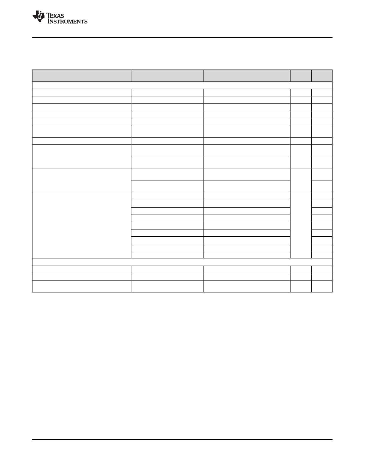
Electrical Characteristics (continued)
Minimum and maximum specifications are at TA= –40°C to 125°C. Typical specifications are at TA= 25°C.
AVDD = 5 V, DVDD = 3 V, V
PARAMETER TEST CONDITIONS MIN TYP MAX UNIT
SYSTEM PERFORMANCE
Resolution 14 Bits A
NMC No missing codes 14 Bits A
DNL Differential nonlinearity –0.5 ±0.2 0.5 LSB
INL Integral nonlinearity
E
G
E
O
SAMPLING DYNAMICS
t
CONV
t
ACQ
f
S
(3) LSB = least significant bit.
(4) This parameter is the endpoint INL, not best-fit INL.
(5) FSR = full-scale range.
(6) Does not include the shift in offset over time.
Gain error At TA= 25°C, all input ranges ±0.02 ±0.05 %FSR
Gain error matching
(channel-to-channel)
Gain error temperature drift All input ranges 1 4 ppm/°C B
Offset error mV
Offset error matching
(channel-to-channel)
Offset error temperature drift Input range = ±0.15625 × V
Conversion time 850 ns A
Acquisition time 1150 ns A
Maximum throughput rate
without latency
= 4.096 V (internal), and f
REF
(4)
At TA= 25°C, all input ranges ±0.02 ±0.05 %FSR A
At TA= 25°C,
input range = ±2.5 × V
At TA= 25°C,
all other input ranges
At TA= 25°C,
input range = ±2.5 × V
At TA= 25°C,
all other input ranges
Input range = ±2.5 × V
Input range = ±1.25 × V
Input range = ±0.625 × V
Input range = ±0.3125 × V
Input range = 0 to 2.5 × V
Input range = 0 to 1.25 × V
Input range = 0 to 0.625 × V
Input range = 0 to 0.3125 × V
= 500 kSPS, unless otherwise noted.
SAMPLE
–0.75 ±0.25 0.75 LSB A
(6)
REF
(6)
REF
REF
REF
REF
REF
REF
REF
REF
REF
REF
LEVEL
(3)
(5)
±0.5 ±1 A
±0.5 ±2 A
±0.5 ±1 A
mV
±0.5 ±2 A
1 3 B
1 3 B
1 3 B
2 6 B
4 12 ppm/°C B
1 3 B
1 3 B
2 6 B
4 12 B
500 kSPS A
TEST
A
A
(1)
Copyright © 2015, Texas Instruments Incorporated Submit Documentation Feedback 7
Product Folder Links: ADS8674 ADS8678
ADS8674,ADS8678
SBAS627 –JULY 2015
www.ti.com
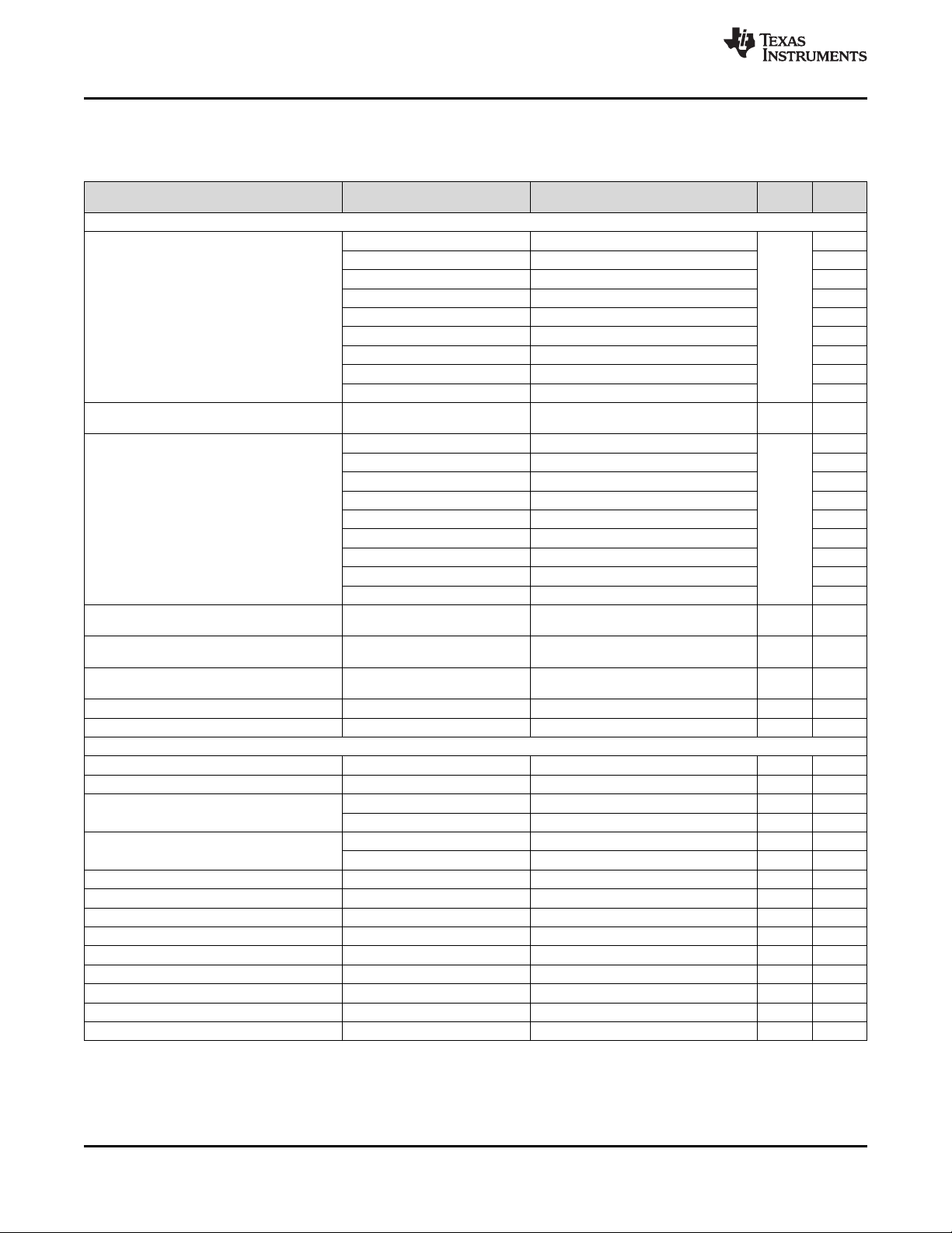
Electrical Characteristics (continued)
Minimum and maximum specifications are at TA= –40°C to 125°C. Typical specifications are at TA= 25°C.
AVDD = 5 V, DVDD = 3 V, V
PARAMETER TEST CONDITIONS MIN TYP MAX UNIT
DYNAMIC CHARACTERISTICS
SNR Input range = ±0.15625 × V
THD All input ranges –100 dB B
SINAD Input range = ±0.15625 × V
SFDR All input ranges 101 dB B
BW
(–3 dB)
BW
(–0.1 dB)
AUXILIARY CHANNEL
V
(AUX_IN)
C
i
I
Ikg(in)
DNL Differential nonlinearity –0.75 ±0.5 0.75 LSB A
INL Integral nonlinearity –1 ±0.5 1 LSB A
E
G(AUX)
E
O(AUX)
SNR Signal-to-noise ratio V
THD Total harmonic distortion
SINAD Signal-to-noise + distortion V
SFDR Spurious-free dynamic range V
(7) Calculated on the first nine harmonics of the input frequency.
(8) Isolation crosstalk is measured by applying a full-scale sinusoidal signal up to 10 kHz to a channel, not selected in the multiplexing
sequence, and measuring its effect on the output of any selected channel.
(9) Memory crosstalk is measured by applying a full-scale sinusoidal signal up to 10 kHz to a channel that is selected in the multiplexing
sequence, and measuring its effect on the output of the next selected channel for all combinations of input channels.
Signal-to-noise ratio
(VIN– 0.5 dBFS at 1 kHz)
Total harmonic distortion
(VIN– 0.5 dBFS at 1 kHz)
Signal-to-noise ratio
(VIN– 0.5 dBFS at 1 kHz)
Spurious-free dynamic range
(VIN– 0.5 dBFS at 1 kHz)
Crosstalk isolation
Crosstalk memory
Small-signal bandwidth, –3 dB At TA= 25°C, all input ranges 15 kHz B
Small-signal bandwidth, –0.1 dB At TA= 25°C, all input ranges 2.5 kHz B
Resolution 14 Bits A
AUX_IN voltage range (AUX_IN – AUX_GND) 0 V
Operating input range
Input capacitance
Input leakage current 100 nA A
Gain error At TA= 25°C ±0.02 ±0.2 %FSR A
Offset error At TA= 25°C –5 5 mV A
= 4.096 V (internal), and f
REF
Input range = ±2.5 × V
Input range = ±1.25 × V
Input range = ±0.625 × V
Input range = ±0.3125 × V
Input range = 2.5 × V
Input range = 1.25 × V
Input range = 0.625 × V
Input range = 0.3125 × V
(7)
Input range = ±2.5 × V
Input range = ±1.25 × V
Input range = ±0.625 × V
Input range = ±0.3125 × V
Input range = 2.5 × V
Input range = 1.25 × V
Input range = 0.625 × V
Input range = 0.3125 × V
(8)
(9)
Aggressor channel input overdriven
to 2 × maximum input voltage
Aggressor channel input overdriven
to 2 × maximum input voltage
AUX_IN 0 V
AUX_GND 0 V A
During sampling 75 pF C
During conversion 5 pF C
(7)
(AUX_IN)
V
(AUX_IN)
(AUX_IN)
(AUX_IN)
= 500 kSPS, unless otherwise noted.
SAMPLE
TEST
LEVEL
REF
REF
REF
REF
REF
REF
REF
REF
REF
REF
REF
REF
REF
REF
REF
REF
REF
REF
84.5 85 A
84.2 85 A
83.5 84.5 A
80 82 A
75 77 dB A
84 85 A
83.5 84.5 A
80 82 A
75 77 A
84.3 84.8 A
84 84.8 A
83.3 84.3 A
80 82 A
75 77 dB A
83.8 84.8 A
83.3 84.3 A
80 82 A
75 77 A
110 dB B
90 dB B
V A
REF
V A
REF
= –0.5 dBFS at 1 kHz 83.3 84.4 dB A
= –0.5 dBFS at 1 kHz –100 dB B
= –0.5 dBFS at 1 kHz 83 84.3 dB A
= –0.5 dBFS at 1 kHz 100 dB B
(1)
8 Submit Documentation Feedback Copyright © 2015, Texas Instruments Incorporated
Product Folder Links: ADS8674 ADS8678
ADS8674,ADS8678
www.ti.com
SBAS627 –JULY 2015
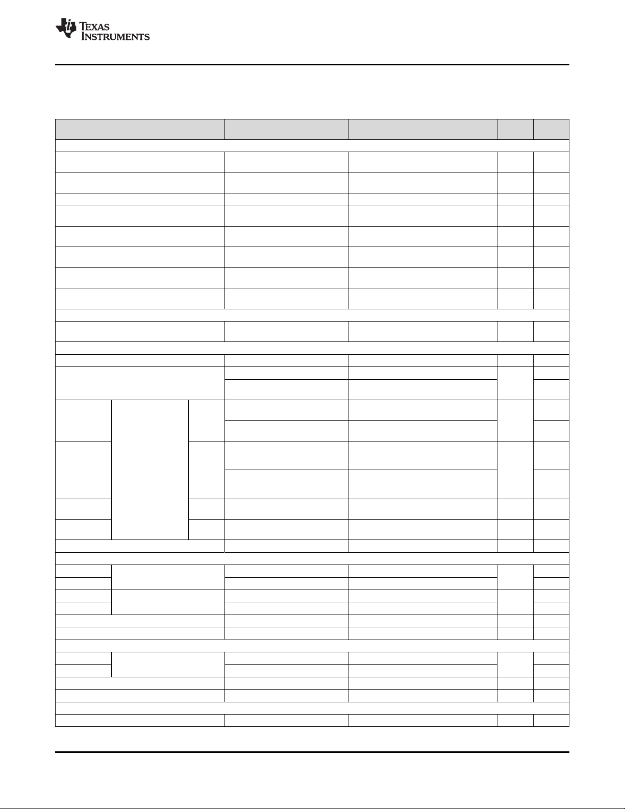
Electrical Characteristics (continued)
Minimum and maximum specifications are at TA= –40°C to 125°C. Typical specifications are at TA= 25°C.
AVDD = 5 V, DVDD = 3 V, V
PARAMETER TEST CONDITIONS MIN TYP MAX UNIT
INTERNAL REFERENCE OUTPUT
Voltage on REFIO pin
(REFIO_INT)
(OUT_REFIO)
(REFCAP)
(OUT_REFCAP)
REFIO_EXT
IH
IL
IH
IL
OH
OL
A
(10)
(configured as output)
Internal reference temperature
drift
Decoupling capacitor on REFIO 10 22 µF B
Reference voltage to ADC
(on REFCAP pin)
Reference buffer output
impedance
Reference buffer temperature
drift
Decoupling capacitor on
REFCAP
Turn-on time 15 ms B
External reference voltage on
REFIO (configured as input)
Analog supply current Static mA
Digital supply current At DVDD = 3.3 V, output = 0000h 0.5 mA A
Digital input logic levels
DVDD > 2.1 V
Digital input logic levels
DVDD ≤ 2.1 V
Input leakage current 100 nA A
Input pin capacitance 5 pF C
Digital output logic levels V
Floating state leakage current Only for SDO 1 µA A
Internal pin capacitance 5 pF C
Operating free-air temperature –40 125 °C B
V
C
V
C
EXTERNAL REFERENCE INPUT
V
POWER-SUPPLY REQUIREMENTS
AVDD Analog power-supply voltage Analog supply 4.75 5 5.25 V B
DVDD Digital power-supply voltage V
I
AVDD_DYN
I
AVDD_STC
I
STDBY
I
PWR_DN
I
DVDD_DYN
DIGITAL INPUTS (CMOS)
V
V
V
V
DIGITAL OUTPUTS (CMOS)
V
V
TEMPERATURE RANGE
T
(10) Does not include the variation in voltage resulting from solder-shift and long-term effects.
= 4.096 V (internal), and f
REF
= 500 kSPS, unless otherwise noted.
SAMPLE
At TA= 25°C 4.094 4.096 4.098 V A
8 20 ppm/°C B
At TA= 25°C 4.094 4.096 4.098 V A
0.5 1 Ω B
0.6 1.5 ppm/°C B
10 22 μF B
C
(OUT_REFCAP)
C
(OUT_REFIO)
= 22 µF,
= 22 µF
4.046 4.096 4.146 V C
Digital supply range 1.65 3.3 AVDD B
Dynamic,
AVDD
Digital supply range for specified
performance
For the ADS8678; AVDD = 5 V, fS=
maximum and internal reference
For the ADS8674; AVDD = 5 V, fS=
maximum and internal reference
2.7 3.3 5.25 B
13 16 A
8.5 11.5 A
For the ADS8678; AVDD = 5 V,
device not converting and internal 10 12 A
reference
For the ADS8674; AVDD = 5 V,
device not converting and internal 5.5 8.5 A
reference
Standby 3 4.5 mA A
Power-
down
At AVDD = 5 V, device in STDBY
mode and internal reference
At AVDD = 5 V, device in PWR_DN 3 20 μA B
0.7 × DVDD DVDD + 0.3 A
–0.3 0.3 × DVDD A
0.8 × DVDD DVDD + 0.3 A
–0.3 0.2 × DVDD A
IO= 500-μA source 0.8 × DVDD DVDD A
IO= 500-μA sink 0 0.2 × DVDD A
LEVEL
mA
V
V
TEST
(1)
Copyright © 2015, Texas Instruments Incorporated Submit Documentation Feedback 9
Product Folder Links: ADS8674 ADS8678
1 2 14 15 16 17
23 24
25
26
27 28 29
30SCLK
CS
D7#2D6#2D5
#2
D4#2D3
#2
D2
#2
SDO
t
SU_CSCK
t
DV_CSDO
t
HT_CKDO
t
SU_DOCK
t
DZ_CSDO
Sample
N
Sample
N + 1
t
ACQ
t
CONV
t
S
Data from sample N
t
PH_CS
31 32
D13
#2
D12
#2
18
D1#2D0
#2
B15
B14 B2
B1 B0 X X
X X X X
SDI
X
X X X X X
t
PH_CK
t
PL_CK
t
SCLK
t
SU_DICK
t
HT_CKDI
t
D_CKCS
7 8 9
B9 B8 B7B10
B3
D7#1D6#1D5
#1
D4#1D3
#1
D2
#1
DAISY
D13
#1
D12
#1
D1#1D0
#1
t
HT_CKDSY
t
SU_DSYCK
ADS8674,ADS8678
SBAS627 –JULY 2015
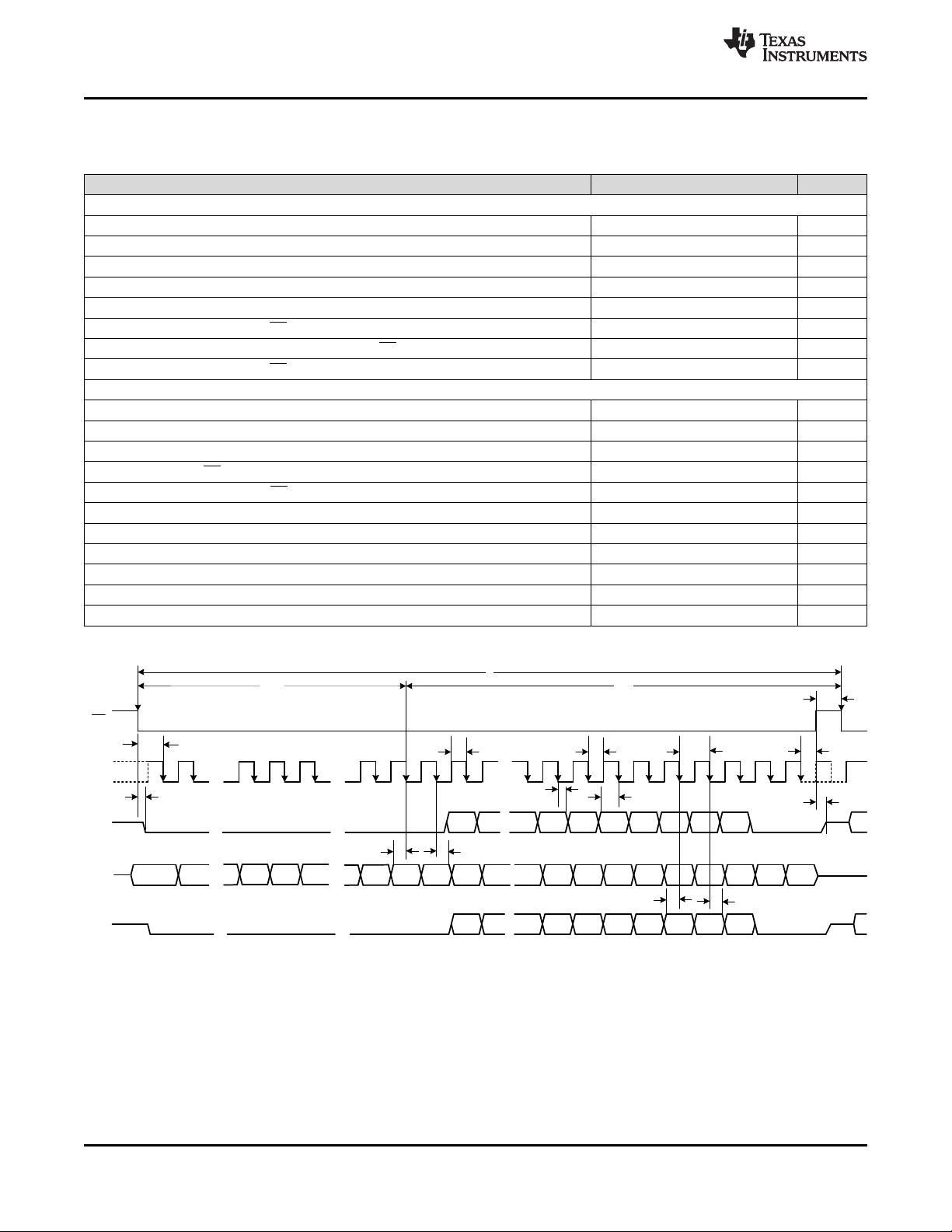
7.6 Timing Requirements: Serial Interface
Minimum and maximum specifications are at TA= –40°C to 125°C. Typical specifications are at TA= 25°C.
AVDD = 5 V, DVDD = 3 V, V
TIMING SPECIFICATIONS
f
S
t
S
f
SCLK
t
SCLK
t
CONV
t
DZ_CSDO
t
D_CKCS
t
DZ_CSDO
TIMING REQUIREMENTS
t
ACQ
t
PH_CK
t
PL_CK
t
PH_CS
t
SU_CSCK
t
HT_CKDO
t
SU_DOCK
t
SU_DICK
t
HT_CKDI
t
SU_DSYCK
t
HT_CKDSY
Sampling frequency (f
ADC cycle time period (f
Serial clock frequency (fS= max) 17 MHz
Serial clock time period (fS= max) 59 ns
Conversion time 850 ns
Delay time: CS falling to data enable 10 ns
Delay time: last SCLK falling to CS rising 10 ns
Delay time: CS rising to SDO going to 3-state 10 ns
Acquisition time 1150 ns
Clock high time 0.4 0.6 t
Clock low time 0.4 0.6 t
CS high time 30 ns
Setup time: CS falling to SCLK falling 30 ns
Hold time: SCLK falling to (previous) data valid on SDO 10 ns
Setup time: SDO data valid to SCLK falling 25 ns
Setup time: SDI data valid to SCLK falling 5 ns
Hold time: SCLK falling to (previous) data valid on SDI 5 ns
Setup time: DAISY data valid to SCLK falling 5 ns
Hold time: SCLK falling to (previous) data valid on DAISY 5 ns
= 4.096 V (internal), SDO load = 20 pF, and f
REF
= max) 500 kSPS
CLK
= max) 2 µs
CLK
= 500 kSPS, unless otherwise noted.
SAMPLE
MIN TYP MAX UNIT
www.ti.com
SCLK
SCLK
10 Submit Documentation Feedback Copyright © 2015, Texas Instruments Incorporated
Figure 1. Serial Interface Timing Diagram
Product Folder Links: ADS8674 ADS8678
0
3000
6000
9000
12000
8189 8190 8191 8192 8193 8194 8195
Number of Hits
Output Codes
C007
0
1000
2000
3000
4000
5000
6000
8189 8190 8191 8192 8193 8194 8195
Number of Hits
Output Codes
C008
-70
0
70
140
210
280
350
±40 ±7
26 59 92 125
Input Impedance Variation ()
Free-Air Temperature (oC)
C005
---- ± 2.5*V
REF,
---- 1.25*V
REF
---- 0.625*V
REF,
------0.3125*V
REF
-------0.156 V
REF,
---- + 2.5*V
REF
---- + 1.25*V
REF,
---- + 0.625*V
REF
---- + 0.3125*V
REF
0
160
320
480
640
800
0.85 0.88 0.91 0.94 0.97 1 1.03 1.06 1.09 1.12 1.15
Number of Samples
Input Impedance (M)
C006
±15
±9
±3
3
9
15
±10 ±6 ±2
2 6 10
Analog Input Current (µA)
Input Voltage (V) C001
---- ± 2.5*V
REF,
---- 1.25*V
REF
---- 0.625*V
REF,
------0.3125*V
REF
-------0.156 V
REF,
---- + 2.5*V
REF
---- + 1.25*V
REF,
---- + 0.625*V
REF
---- + 0.3125*V
REF
±15
±9
±3
3
9
15
±10 ±6 ±2
2 6 10
Analog Input Current (µA)
Input Voltage (V)
C002
----- -400C
----- 250C
----- 1250C
www.ti.com
7.7 Typical Characteristics
At TA= 25°C, AVDD = 5 V, DVDD = 3 V, internal reference V
= 4.096 V, and f
REF
ADS8674,ADS8678
SBAS627 –JULY 2015
= 500 kSPS, unless otherwise noted.
SAMPLE
Input range = ±2.5 × V
REF
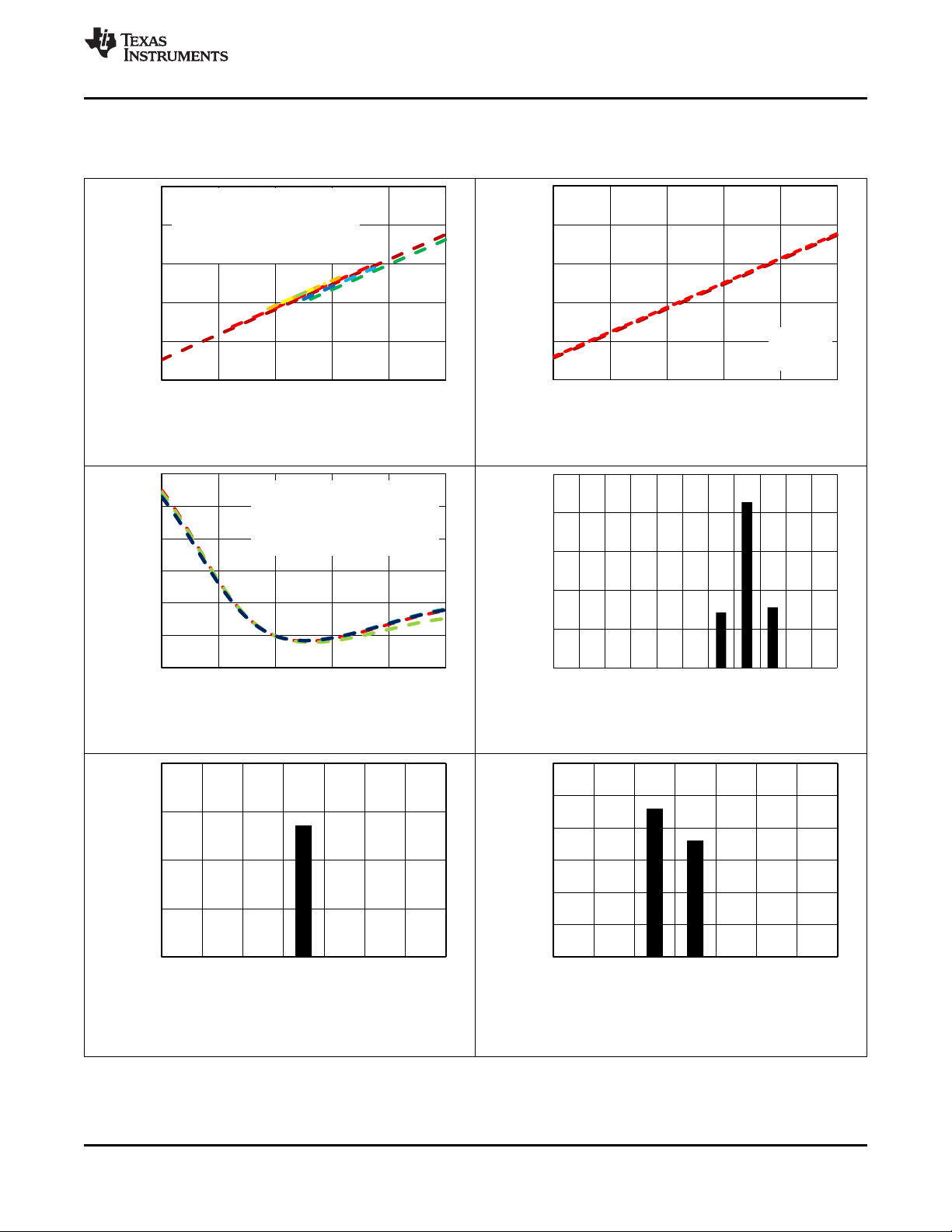
Figure 2. Input I-V Characteristic Figure 3. Input Current vs Temperature
Number of samples = 1160
Figure 4. Input Impedance Variation vs Temperature Figure 5. Typical Distribution of Input Impedance
Copyright © 2015, Texas Instruments Incorporated Submit Documentation Feedback 11
Mean = 8192.5, sigma = 0.31, input = 0 V, Mean = 8192.5, sigma = 0.32, input = 0 V,
Figure 6. DC Histogram for Mid-Scale Inputs (±2.5 × V
range = ±2.5 × V
REF
range = ±1.25 × V
) Figure 7. DC Histogram for Mid-Scale Inputs (±1.25 × V
REF
Product Folder Links: ADS8674 ADS8678
REF
REF
)
0
1000
2000
3000
4000
5000
6000
8189 8190 8191 8192 8193 8194 8195 8196
Number of Hits
Output Codes
C013
0
1000
2000
3000
4000
5000
6000
8190 8191 8192 8193 8194 8195
Number of Hits
Output Codes
C014
0
2000
4000
6000
8000
10000
8187 8189 8191 8193 8195
Number of Hits
Output Codes
C011
0
1000
2000
3000
4000
5000
6000
8190 8191 8192 8193 8194 8195
Number of Hits
Output Codes
C012
0
2000
4000
6000
8000
8187 8188 8189 8190 8191 8192 8193 8194 8195
Number of Hits
Output Codes
C009
0
2000
4000
6000
8000
10000
8188 8189 8190 8191 8192 8193 8194 8195 8196
Number of Hits
Output Codes
C010
ADS8674,ADS8678
SBAS627 –JULY 2015
Typical Characteristics (continued)
www.ti.com
At TA= 25°C, AVDD = 5 V, DVDD = 3 V, internal reference V
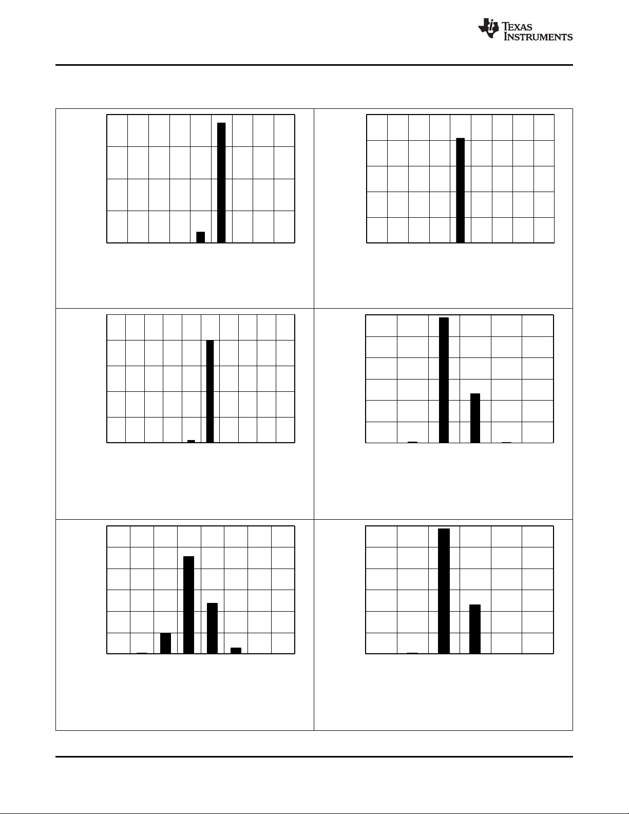
Mean = 8192.5, sigma = 0.34, input = 0 V, Mean = 8192.5, sigma = 0.32, input = 1.25 × V
Figure 8. DC Histogram for Mid-Scale Inputs (±0.625 × V
range = ±0.625 × V
REF
REF
= 4.096 V, and f
REF
= 500 kSPS, unless otherwise noted.
SAMPLE
range = 2.5 × V
REF
REF
,
) Figure 9. DC Histogram for Mid-Scale Inputs (2.5 × V
REF
)
Mean = 8192.5, sigma = 0.34, input = 0.625 × V
range = 1.25 × V
Figure 10. DC Histogram for Mid-Scale Inputs Figure 11. DC Histogram for Mid-Scale Inputs
12 Submit Documentation Feedback Copyright © 2015, Texas Instruments Incorporated
Mean = 8192.5, sigma = 0.72, input = 0 V, Mean = 8192.5, sigma = 0.72, input = 0.3125 × V
range = ±0.15625 × V
Figure 12. DC Histogram for Mid-Scale Inputs Figure 13. DC Histogram for Mid-Scale Inputs
(±0.15625 x V
(1.25 × V
, Mean = 8192.5, sigma = 0.43, input = 0 V,
REF
) (±0.3125 x V
REF
REF
) (0.625 x V
REF
REF
range = ±0.3125 × V
range = 0.625 × V
Product Folder Links: ADS8674 ADS8678
REF
REF
REF
REF
)
)
,
REF
-0.5
-0.3
-0.1
0.1
0.3
0.5
0 4096 8192 12288 16384
Integral Nonlinearity (LSB)
Codes (LSB)
C019
-0.5
-0.3
-0.1
0.1
0.3
0.5
0 4096 8192 12288 16384
Integral Nonlinearity (LSB)
Codes (LSB)
C020
-0.5
-0.3
-0.1
0.1
0.3
0.5
±40 ±7
26 59 92 125
Differential Nonlinearity (LSB)
Free-Air Temperature (oC)
C017
Maximum
Minimum
-0.5
-0.25
0
0.25
0.5
0 4096 8192 12288 16384
Integral Nonlinearity (LSB)
Codes (LSB)
C018
0
1000
2000
3000
4000
5000
6000
8189 8190 8191 8192 8193 8194 8195 8196
Number of Hits
Output Codes
C015
-0.5
-0.3
-0.1
0.1
0.3
0.5
0 4096 8192 12288 16384
Differential Nonlinearity (LSB)
Codes (LSB)
C016
www.ti.com
Typical Characteristics (continued)
ADS8674,ADS8678
SBAS627 –JULY 2015
At TA= 25°C, AVDD = 5 V, DVDD = 3 V, internal reference V
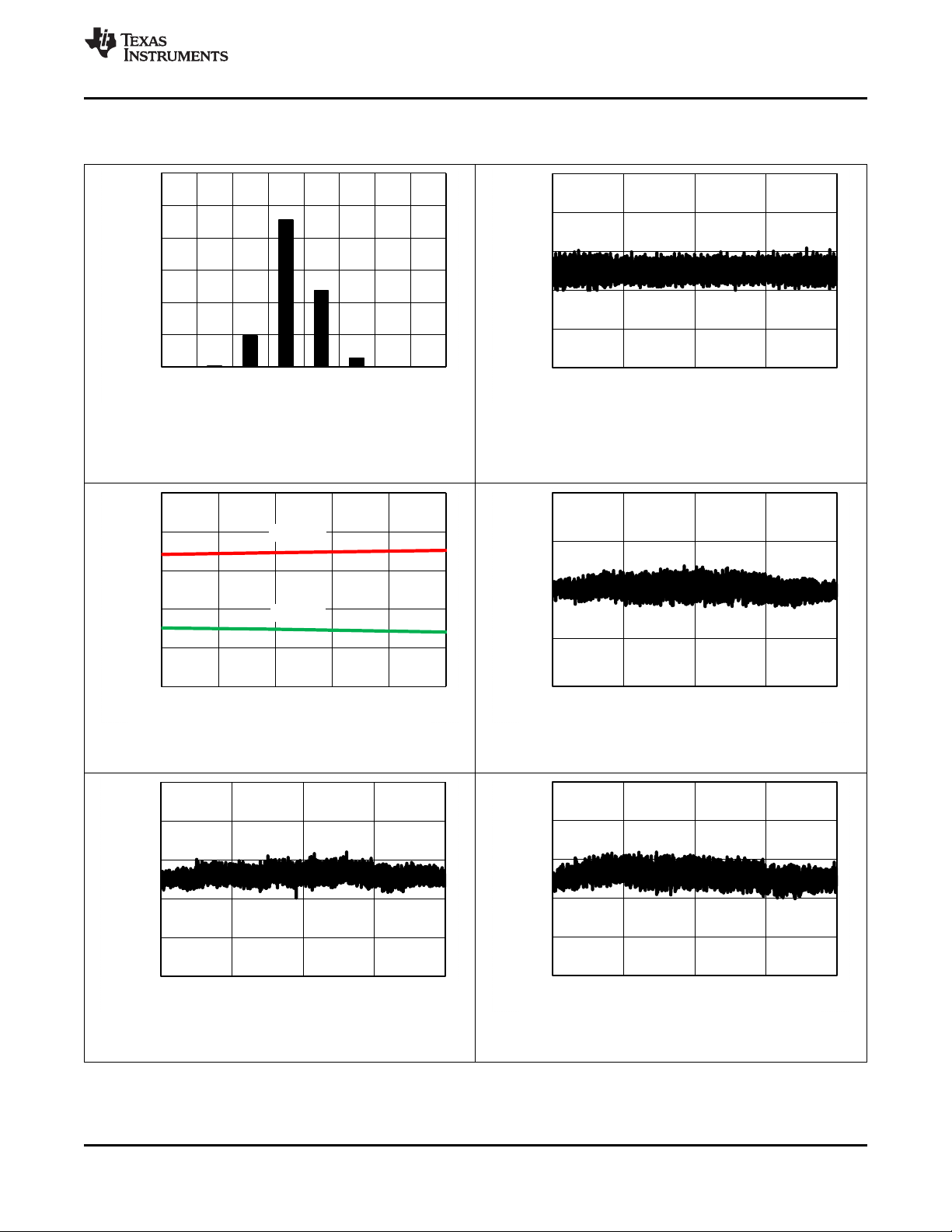
Mean = 8192.5, sigma = 0.750.72, input = 0.15625 × V
range = 0.3125 × V
REF
Figure 14. DC Histogram for Mid-Scale Inputs
(0.3125 x V
REF
)
, All input ranges
REF
= 4.096 V, and f
REF
= 500 kSPS, unless otherwise noted.
SAMPLE
Figure 15. Typical DNL for All Codes
All input ranges Range = ±2.5 × V
Figure 16. DNL vs Temperature Figure 17. Typical INL for All Codes
Copyright © 2015, Texas Instruments Incorporated Submit Documentation Feedback 13
Range = ±1.25 × V
Figure 18. Typical INL for All Codes Figure 19. Typical INL for All Codes
REF
Product Folder Links: ADS8674 ADS8678
Range = ±0.625 × V
REF
REF
-0.5
-0.3
-0.1
0.1
0.3
0.5
0 4096 8192 12288 16384
Integral Nonlinearity (LSB)
Codes (LSB)
C025
-0.5
-0.3
-0.1
0.1
0.3
0.5
0 4096 8192 12288 16384
Integral Nonlinearity (LSB)
Codes (LSB)
C026
-0.5
-0.3
-0.1
0.1
0.3
0.5
0 4096 8192 12288 16384
Integral Nonlinearity (LSB)
Codes (LSB)
C023
-0.5
-0.3
-0.1
0.1
0.3
0.5
0 4096 8192 12288 16384
Integral Nonlinearity (LSB)
Codes (LSB)
C024
-0.5
-0.3
-0.1
0.1
0.3
0.5
0 4096 8192 12288 16384
Integral Nonlinearity (LSB)
Codes (LSB)
C021
-0.5
-0.3
-0.1
0.1
0.3
0.5
0 4096 8192 12288 16384
Integral Nonlinearity (LSB)
Codes (LSB)
C022
ADS8674,ADS8678
SBAS627 –JULY 2015
Typical Characteristics (continued)
www.ti.com
At TA= 25°C, AVDD = 5 V, DVDD = 3 V, internal reference V
Range = 2.5 × V
Figure 20. Typical INL for All Codes Figure 21. Typical INL for All Codes
REF
= 4.096 V, and f
REF
= 500 kSPS, unless otherwise noted.
SAMPLE
Range = 1.25 × V
REF
Range = ±0.3125 × V
REF
Range = ±0.15625 × V
REF
Figure 22. Typical INL for All Codes Figure 23. Typical INL for All Codes
Range = 0.625 × V
REF
Range = 0.3125 × V
REF
Figure 24. Typical INL for All Codes Figure 25. Typical INL for All Codes
14 Submit Documentation Feedback Copyright © 2015, Texas Instruments Incorporated
Product Folder Links: ADS8674 ADS8678
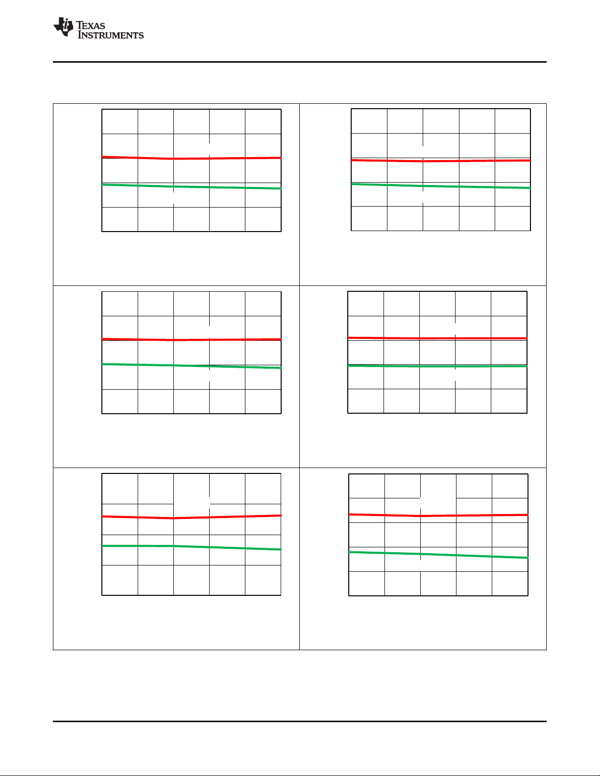
-0.5
-0.25
0
0.25
0.5
±40 ±7
26 59 92 125
Integgral Nonlinearity (LSB)
Free-Air Temperature (oC)
C031
Minimum
Maximum
-0.5
-0.3
-0.1
0.1
0.3
0.5
±40 ±7
26 59 92 125
Integral Nonlinearity (LSB)
Free- Air Temperature (oC)
C032
Minimum
Maximum
-0.5
-0.3
-0.1
0.1
0.3
0.5
±40 ±7
26 59 92 125
Integral Nonlinearity (LSB)
Free-Air Temperature (oC)
C029
Minimum
Maximum
-0.5
-0.3
-0.1
0.1
0.3
0.5
±40 ±7
26 59 92 125
Integral Nonlinearity (LSB)
Free-Air Temperature (oC)
C030
Maximum
Minimum
-0.5
-0.3
-0.1
0.1
0.3
0.5
±40 ±7
26 59 92 125
Integral Nonlinearity (LSB)
Free-Air Temperature (oC)
C027
Minimum
Maximum
-0.5
-0.3
-0.1
0.1
0.3
0.5
±40 ±7
26 59 92 125
Integral Nonlinearity (LSB)
Free-Air Temperature (oC)
C028
Maximum
Minimum
www.ti.com
Typical Characteristics (continued)
ADS8674,ADS8678
SBAS627 –JULY 2015
At TA= 25°C, AVDD = 5 V, DVDD = 3 V, internal reference V
Range = ±2.5 × V
Figure 26. INL vs Temperature (±2.5 × V
REF
) Figure 27. INL vs Temperature (±1.25 × V
REF
= 4.096 V, and f
REF
= 500 kSPS, unless otherwise noted.
SAMPLE
Range = ±1.25 × V
REF
REF
)
Range = ±0.625 × V
Figure 28. INL vs Temperature (±0.625 × V
Range = 1.25 × V
Figure 30. INL vs Temperature (1.25 × V
Copyright © 2015, Texas Instruments Incorporated Submit Documentation Feedback 15
REF
REF
) Figure 29. INL vs Temperature (2.5 × V
REF
) Figure 31. INL vs Temperature (±0.3125 × V
REF
Range = 2.5 × V
REF
Range = ±0.3125 × V
REF
REF
Product Folder Links: ADS8674 ADS8678
)
REF
)
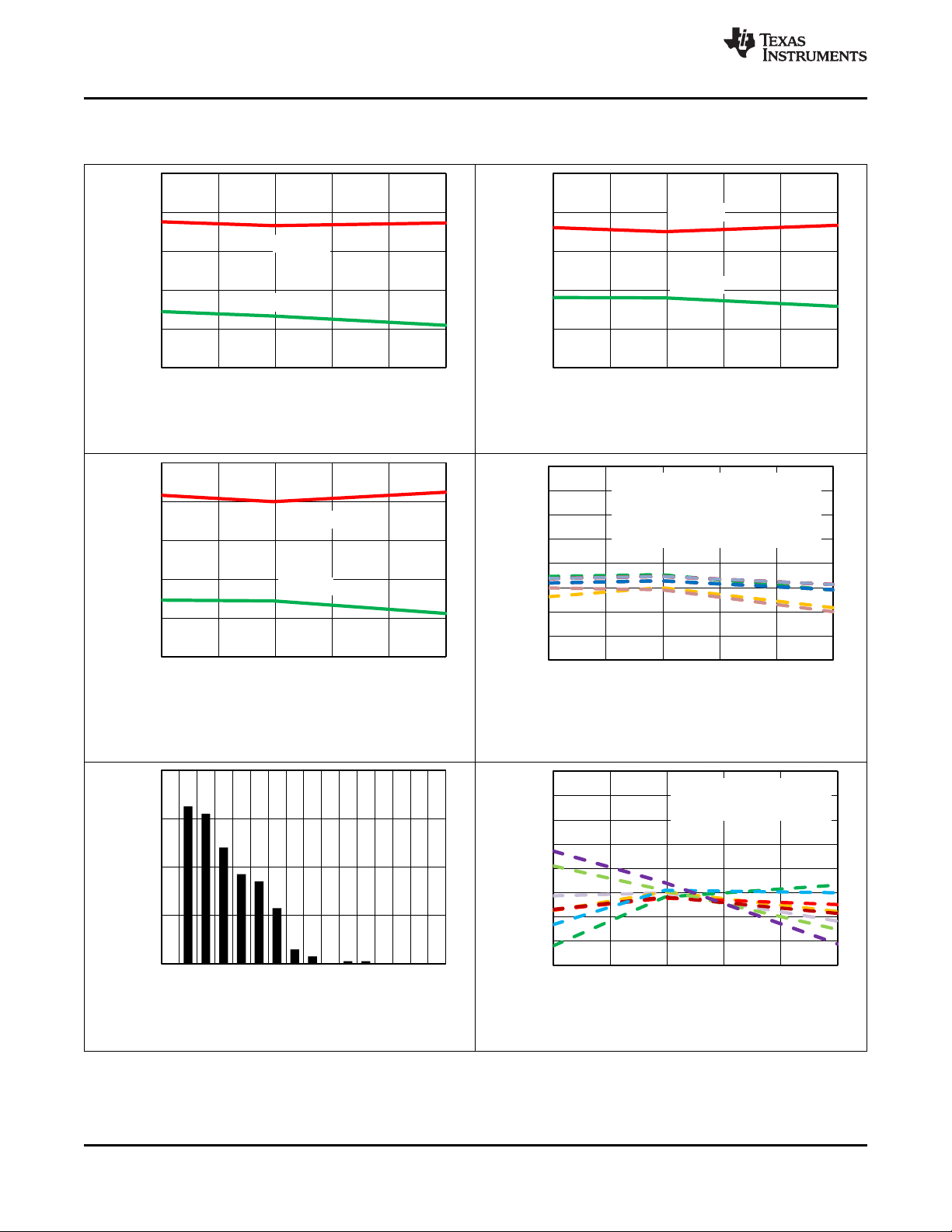
-1
-0.75
-0.5
-0.25
0
0.25
0.5
0.75
1
±40 ±7
26 59 92 125
Offset Error (mV)
Free-Air Temperature (oC)
C038
......CH0, .......CH1, ......CH2,
.......CH3, ......CH4, .......CH5,
........CH6, .......CH7
0
20
40
60
80
0 0.2 0.4 0.6 0.8 1 1.2 1.4 1.6 1.8 2 2.2 2.4 2.6 2.8 3
Number of Devices
Offset Drift (ppm/oC)
C037
-1
-0.75
-0.5
-0.25
0
0.25
0.5
0.75
1
±40 ±7
26 59 92 125
Offset Error (mV)
Free-Air Temperature (oC)
C036
---- ± 2.5*V
REF,
---- 1.25*V
REF
---- 0.625*V
REF,
------0.3125*V
REF
-------0.156 V
REF,
---- + 2.5*V
REF
---- + 1.25*V
REF,
---- + 0.625*V
REF
---- + 0.3125*V
REF
-0.5
-0.3
-0.1
0.1
0.3
0.5
±40 ±7
26 59 92 125
Integral Nonlinearity (LSB)
Free-Air Temperature (oC)
C035
Maximum
Minimum
-0.5
-0.3
-0.1
0.1
0.3
0.5
±40 ±7
26 59 92 125
Integral Nonlinearity (LSB)
Free-Air Temperature (oC)
C033
Minimum
Maximum
-0.5
-0.3
-0.1
0.1
0.3
0.5
±40 ±7
26 59 92 125
Integral Nonlinearity (LSB)
Free-Air Temperature (oC)
C034
Maximum
Minimum
ADS8674,ADS8678
SBAS627 –JULY 2015
Typical Characteristics (continued)
www.ti.com
At TA= 25°C, AVDD = 5 V, DVDD = 3 V, internal reference V
Range = ±0.15625 × V
Figure 32. INL vs Temperature (±0.15625 × V
REF
) Figure 33. INL vs Temperature (0.625 × V
REF
= 4.096 V, and f
REF
= 500 kSPS, unless otherwise noted.
SAMPLE
Range = 0.625 × V
REF
REF
)
Range = 0.3125 × V
Figure 34. INL vs Temperature (0.3125 × V
REF
REF
)
Figure 35. Offset Error vs
Temperature Across Input Ranges
Figure 36. Typical Histogram for Offset Drift
Range = ±2.5 × V
REF
Figure 37. Offset Error vs Temperature Across Channels
Range = ±2.5 × V
REF
16 Submit Documentation Feedback Copyright © 2015, Texas Instruments Incorporated
Product Folder Links: ADS8674 ADS8678
±160
±120
±80
±40
0
0 50000 100000 150000 200000 250000
Amplitude (dB)
Input Frequency (Hz)
C043
±160
±120
±80
±40
0
0 50000 100000 150000 200000 250000
Amplitude (dB)
Input Frequency (Hz)
C044
-0.05
-0.03
-0.01
0.01
0.03
0.05
±40 ±7
26 59 92 125
Gain (%FS)
Free- Air Temperature (oC)
C041
......CH0, .......CH1, ......CH2,
.......CH3, ......CH4, .......CH5,
........CH6, .......CH7
0
0.5
1
1.5
2
0 4 8 12 16 20
Gain (%FS)
Source Resistance (k)
C042
---- ± 2.5*V
REF,
---- 1.25*V
REF
---- 0.625*V
REF,
------0.3125*V
REF
-------0.156 V
REF,
---- + 2.5*V
REF
---- + 1.25*V
REF,
---- + 0.625*V
REF
---- + 0.3125*V
REF
-0.05
-0.03
-0.01
0.01
0.03
0.05
±40 ±7
26 59 92 125
Gain (% FS)
Free-Air Temperature (oC)
C039
---- ± 2.5*V
REF,
---- 1.25*V
REF
---- 0.625*V
REF,
------0.3125*V
REF
-------0.156 V
REF,
---- + 2.5*V
REF
---- + 1.25*V
REF,
---- + 0.625*V
REF
---- + 0.3125*V
REF
0
20
40
60
80
100
120
140
0 0.5 1 1.5 2 2.5 3 3.5 4
Number of Units
Gain Drift (ppm/oC)
C040
www.ti.com
Typical Characteristics (continued)
ADS8674,ADS8678
SBAS627 –JULY 2015
At TA= 25°C, AVDD = 5 V, DVDD = 3 V, internal reference V
Figure 38. Gain Error vs Temperature Across Input Ranges
= 4.096 V, and f
REF
= 500 kSPS, unless otherwise noted.
SAMPLE
Range = ±2.5 × V
REF
Figure 39. Typical Histogram for Gain Error Drift
Range = ±2.5 × V
Figure 40. Gain Error vs Temperature Across Channels
Copyright © 2015, Texas Instruments Incorporated Submit Documentation Feedback 17
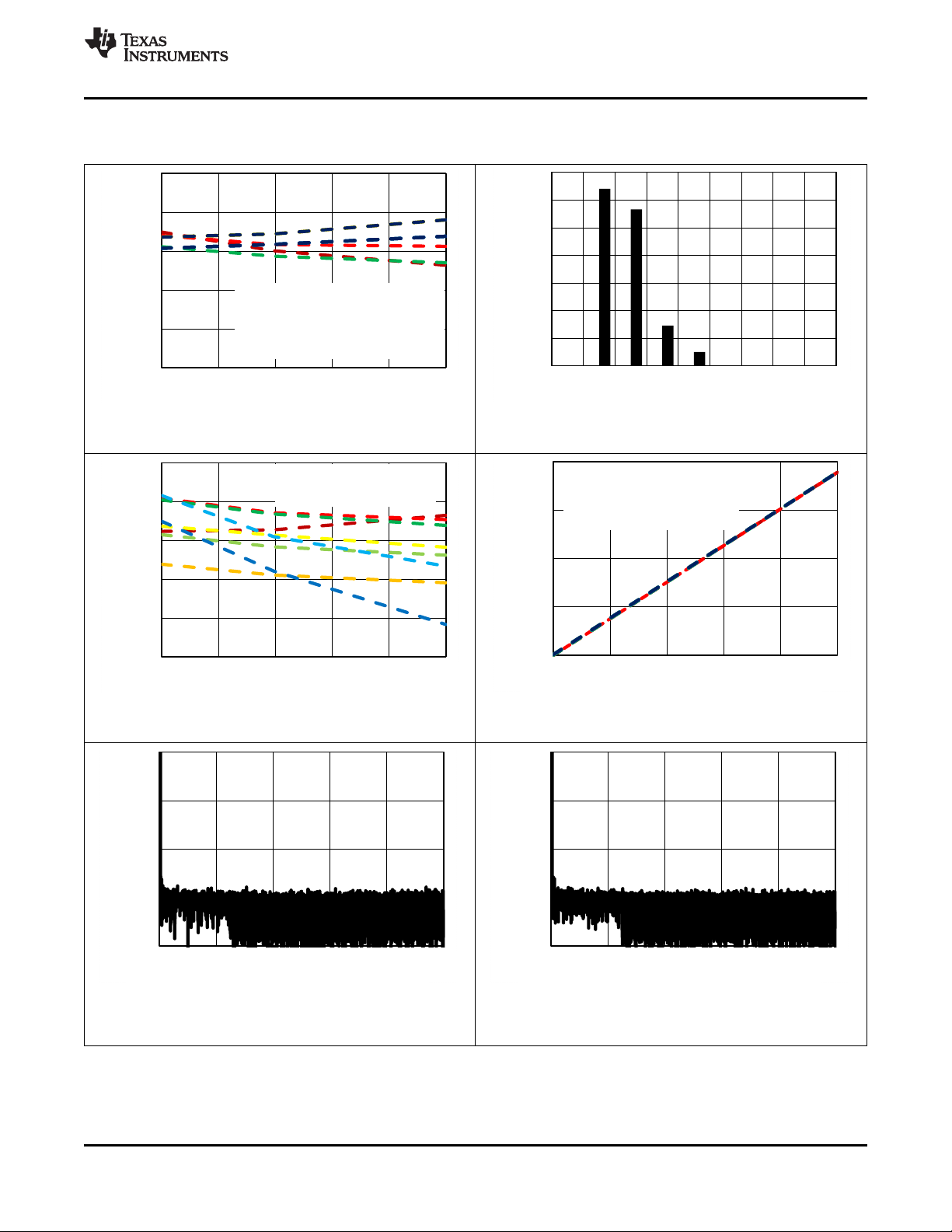
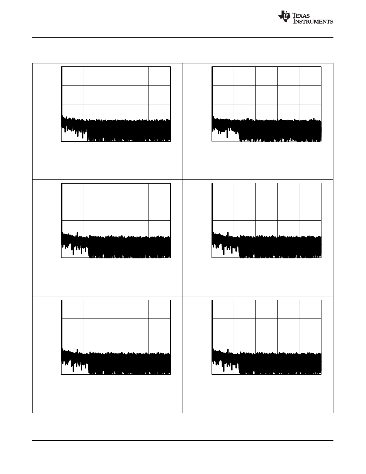
Number of points = 16k, fIN= 1 kHz, SNR = 85.37 dB, Number of points = 16k, fIN= 1 kHz, SNR = 85.11 dB,
SINAD = 85.35, THD = –104.68 dB, SFDR = 105 dB SINAD = 85.15 dB, THD = –105.28 dB, SFDR = 105 dB
Figure 42. Typical FFT Plot (±2.5 × V
REF
) Figure 43. Typical FFT Plot (±1.25 × V
REF
Product Folder Links: ADS8674 ADS8678
Figure 41. Gain Error vs External Resistance (R
REF
)
EXT
)
±160
±120
±80
±40
0
0 50000 100000 150000 200000 250000
Amplitude (dB)
Input Frequency (Hz)
C049
±160
±120
±80
±40
0
0 50000 100000 150000 200000 250000
Amplitude (dB)
Input Frequency (Hz)
C050
±160
±120
±80
±40
0
0 50000 100000 150000 200000 250000
Amplitude (dB)
Input Frequency (Hz)
C047
±160
±120
±80
±40
0
0 50000 100000 150000 200000 250000
Amplitude (dB)
Input Frequency (Hz)
C048
±160
±120
±80
±40
0
0 50000 100000 150000 200000 250000
Amplitude (dB)
Input Frequency (Hz)
C045
±160
±120
±80
±40
0
0 50000 100000 150000 200000 250000
Amplitude (dB)
Input Frequency (Hz)
C046
ADS8674,ADS8678
SBAS627 –JULY 2015
Typical Characteristics (continued)
www.ti.com
At TA= 25°C, AVDD = 5 V, DVDD = 3 V, internal reference V
= 4.096 V, and f
REF
= 500 kSPS, unless otherwise noted.
SAMPLE
Number of points = 16k, fIN= 1 kHz, SNR = 84.69 dB, Number of points = 16k, fIN= 1 kHz, SNR = 85.04 dB,
SINAD = 84.67 dB, THD = –106.41 dB, SFDR = 105 dB SINAD = 85.04 dB, THD = –106.31 dB, SFDR = 105 dB
Figure 44. Typical FFT Plot (±0.625 × V
) Figure 45. Typical FFT Plot (2.5 × V
REF
REF
)
Number of points = 16k, fIN= 1 kHz, SNR = 84.62 dB, Number of points = 16k, fIN= 1 kHz, SNR = 82.59 dB,
SINAD = 84.65 dB, THD = –103.74 dB, SFDR = 105 dB SINAD = 82.56 dB, THD = –102.41 dB, SFDR = 105 dB
Figure 46. Typical FFT Plot (1.25 × V
Number of points = 16k, fIN= 1 kHz, SNR = 78.09 dB, Number of points = 16k, fIN= 1 kHz, SNR = 82.59 dB,
SINAD = 78.06 dB, THD = –99.41 dB, SFDR = 105 dB SINAD = 82.55 dB, THD = –99.74 dB, SFDR = 105 dB
18 Submit Documentation Feedback Copyright © 2015, Texas Instruments Incorporated
Figure 48. Typical FFT Plot (±0.15625 × V
) Figure 47. Typical FFT Plot (±0.3125 × V
REF
) Figure 49. Typical FFT Plot (0.625 × V
REF
Product Folder Links: ADS8674 ADS8678
REF
REF
)
)
75
79
83
87
91
95
±40 ±7
26 59 92 125
Signal-to-Noise + Distortion Ratio (dB)
Free-Air Temperature (oC)
C055
---- ± 2.5*V
REF,
---- 1.25*V
REF,
---- 0.625*V
REF,
------0.3125*V
REF,
-------0.156 V
REF,
---- + 2.5*V
REF
---- + 1.25*V
REF,
---- + 0.625*V
REF,
---- + 0.3125*V
REF
±120
±115
±110
±105
±100
±95
±90
±85
±80
100 1000 10000
Total Harmonic Distortion (dB)
Input Frequency (Hz)
C056
---- ± 2.5*V
REF,
---- 1.25*V
REF,
---- 0.625*V
REF,
------0.3125*V
REF,
-------0.156 V
REF,
---- + 2.5*V
REF
---- + 1.25*V
REF,
---- + 0.625*V
REF,
---- + 0.3125*V
REF
75
78
81
84
87
90
93
96
±40 ±7
26 59 92 125
Signal-to-Noise Ratio (dB)
Free-Air Temperature (oC)
C053
---- ± 2.5*V
REF,
---- 1.25*V
REF,
---- 0.625*V
REF,
------0.3125*V
REF,
-------0.156 V
REF,
---- + 2.5*V
REF
---- + 1.25*V
REF,
---- + 0.625*V
REF,
---- + 0.3125*V
REF
72
75
78
81
84
87
90
93
100 1000 10000
Signal-to-Noise + Distortion Ratio (dB)
Input Frequency (Hz)
C054
---- ± 2.5*V
REF,
---- 1.25*V
REF,
---- 0.625*V
REF,
------0.3125*V
REF,
-------0.156 V
REF,
---- + 2.5*V
REF
---- + 1.25*V
REF,
---- + 0.625*V
REF,
---- + 0.3125*V
REF
±160
±120
±80
±40
0
0 50000 100000 150000 200000 250000
Amplitude (dB)
Input Frequency (Hz)
C051
75
80
85
90
95
100 1000 10000
Signal-to-Noise Ratio (dB)
Input Frequency (Hz)
C052
---- ± 2.5*V
REF,
---- 1.25*V
REF,
---- 0.625*V
REF,
------0.3125*V
REF,
-------0.156 V
REF,
---- + 2.5*V
REF
---- + 1.25*V
REF,
---- + 0.625*V
REF,
---- + 0.3125*V
REF
www.ti.com
Typical Characteristics (continued)
ADS8674,ADS8678
SBAS627 –JULY 2015
At TA= 25°C, AVDD = 5 V, DVDD = 3 V, internal reference V
Number of points = 16k, fIN= 1 kHz, SNR = 78.09 dB,
SINAD = 78.05 dB, THD = –96.74 dB, SFDR = 105 dB
Figure 50. Typical FFT Plot (0.3125 × V
REF
)
= 4.096 V, and f
REF
= 500 kSPS, unless otherwise noted.
SAMPLE
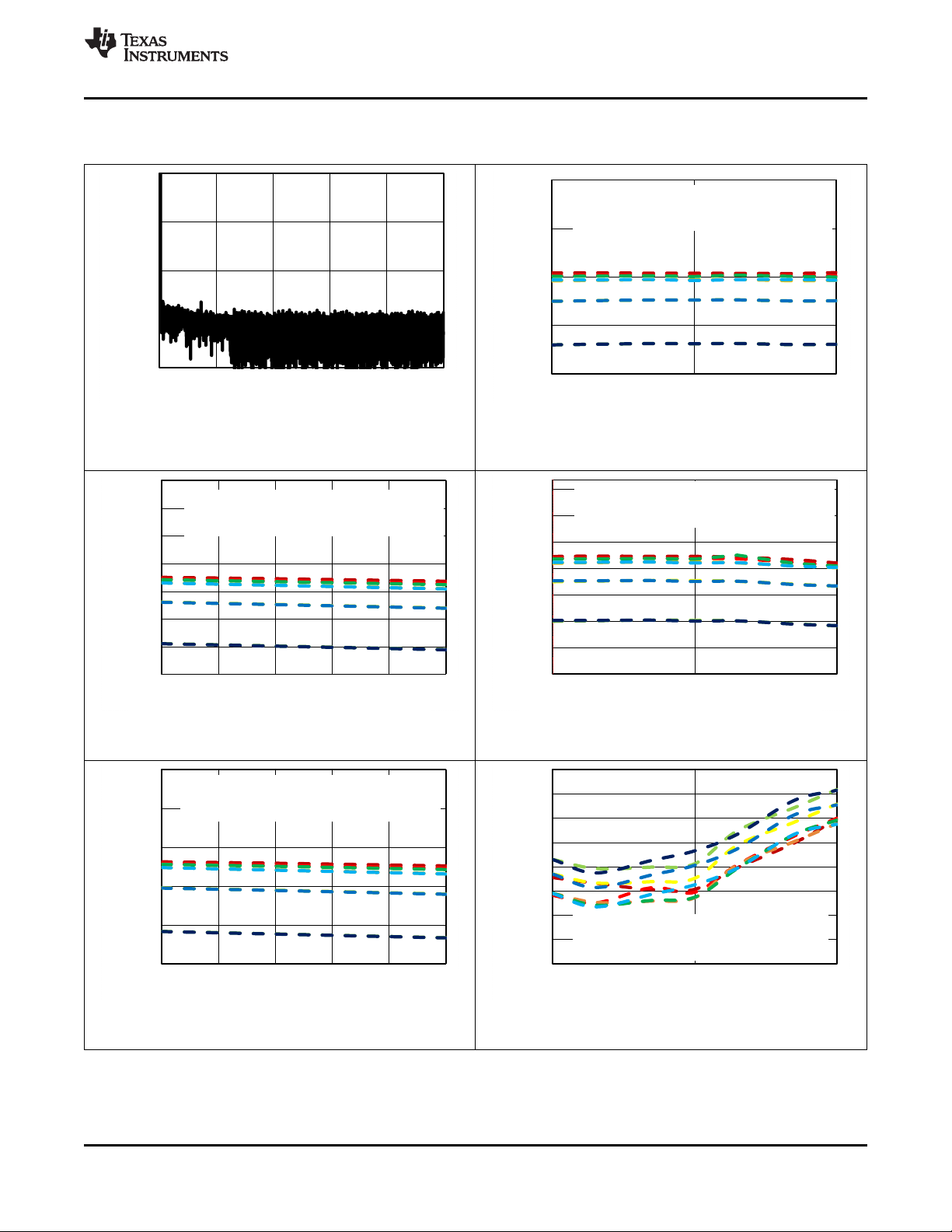
Figure 51. SNR vs Input Frequency
fIN= 1 kHz
Figure 52. SNR vs Temperature Figure 53. SINAD vs Input Frequency
Copyright © 2015, Texas Instruments Incorporated Submit Documentation Feedback 19
Figure 54. SINAD vs Temperature Figure 55. THD vs Input Frequency
fIN= 1 kHz
Product Folder Links: ADS8674 ADS8678
±160
±140
±120
±100
±80
±60
±40
50 500 5000 50000 500000 5000000
Isolation Crosstalk (dB)
Input Frequency (Hz)
C061
---- ± 2.5*V
REF,
---- 1.25*V
REF,
---- 0.625*V
REF,
------0.3125*V
REF,
-------0.156 V
REF,
---- + 2.5*V
REF
---- + 1.25*V
REF,
---- + 0.625*V
REF,
---- + 0.3125*V
REF
10
10.5
11
11.5
12
±40 ±7
26 59 92 125
I
AVDD
Dynamic (mA)
Free-Air Temperature (oC)
C074
±160
±140
±120
±100
±80
±60
±40
50 500 5000 50000 500000 5000000
Memory Crosstalk (dB)
Input Frequency (Hz)
C060
---- ± 2.5*V
REF,
---- 1.25*V
REF,
---- 0.625*V
REF,
------0.3125*V
REF,
-------0.156 V
REF,
---- + 2.5*V
REF
---- + 1.25*V
REF,
---- + 0.625*V
REF,
---- + 0.3125*V
REF
±180
±160
±140
±120
±100
±80
50 500 5000 50000 500000 5000000
Isolation Cross Talk (dB)
Input Frequency (Hz)
C059
---- ± 2.5*V
REF,
---- 1.25*V
REF,
---- 0.625*V
REF,
------0.3125*V
REF,
-------0.156 V
REF,
---- + 2.5*V
REF
---- + 1.25*V
REF,
---- + 0.625*V
REF,
---- + 0.3125*V
REF
±160
±145
±130
±115
±100
±85
±70
50 500 5000 50000 500000 5000000
Memory Crosstalk (dB)
Input Frequency (Hz)
C058
---- ± 2.5*V
REF,
---- 1.25*V
REF,
---- 0.625*V
REF,
------0.3125*V
REF,
-------0.156 V
REF,
---- + 2.5*V
REF
---- + 1.25*V
REF,
---- + 0.625*V
REF,
---- + 0.3125*V
REF
±120
±115
±110
±105
±100
±95
±90
±85
±80
±40 ±7
26 59 92 125
Total Harmonic Distortion (dB)
Free-Air temperature (oC)
C057
---- ± 2.5*V
REF,
---- 1.25*V
REF,
---- 0.625*V
REF,
------0.3125*V
REF,
-------0.156 V
REF,
---- + 2.5*V
REF
---- + 1.25*V
REF,
---- + 0.625*V
REF,
---- + 0.3125*V
REF
ADS8674,ADS8678
SBAS627 –JULY 2015
Typical Characteristics (continued)
www.ti.com
At TA= 25°C, AVDD = 5 V, DVDD = 3 V, internal reference V
fIN= 1 kHz
Figure 56. THD vs Temperature
= 4.096 V, and f
REF
= 500 kSPS, unless otherwise noted.
SAMPLE
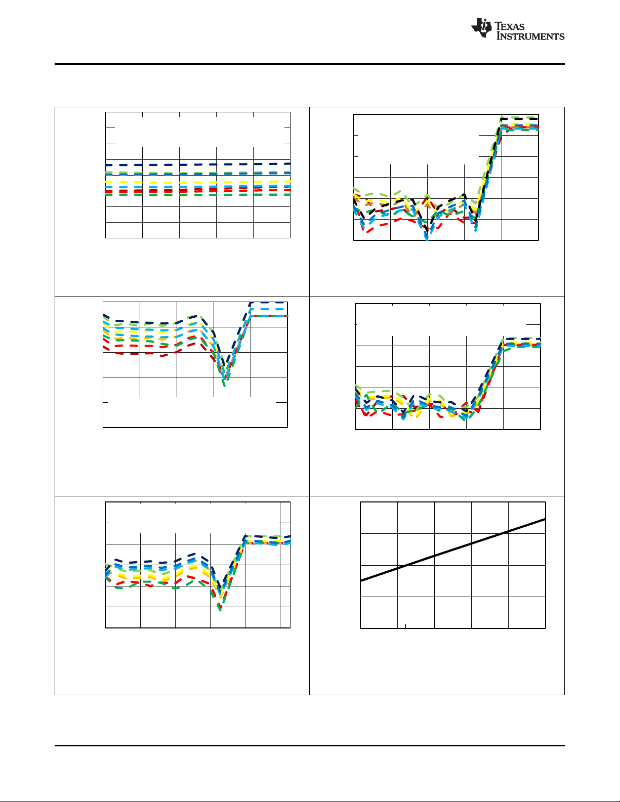
Figure 57. Memory Crosstalk vs Frequency
Figure 58. Isolation Crosstalk vs Frequency
20 Submit Documentation Feedback Copyright © 2015, Texas Instruments Incorporated
Input = 2 × maximum input voltage
Figure 60. Isolation Crosstalk vs Frequency for Figure 61. AVDD Current vs Temperature for the ADS8678
Overrange Inputs (fS= 500 kSPS)
Input = 2 × maximum input voltage
Figure 59. Memory Crosstalk vs Frequency for
Overrange Inputs
Product Folder Links: ADS8674 ADS8678
1
2
3
4
5
6
±40 ±7
26 59 92 125
I
AVDD
PD (uA)
Free-Air Temperature (oC)
C077
4.5
4.75
5
5.25
5.5
5.75
6
±40 ±7
26 59 92 125
I
AVDD
Static (mA)
Free-Air Temperature(oC)
C079
2
2.1
2.2
2.3
±40 ±7
26 59 92 125
I
AVDD
Standby (mA)
Free-Air Temperature (oC)
C076
7.5
7.75
8
8.25
8.5
8.75
9
±40 ±7
26 59 92 125
I
AVDD
Static (mA)
Free-Air Temperature (oC)
C075
7.5
7.75
8
8.25
8.5
8.75
9
±40 ±7
26 59 92 125
I
AVDD
Dynamic (mA)
Free-Air Temperature(oC)
C078
www.ti.com
Typical Characteristics (continued)
ADS8674,ADS8678
SBAS627 –JULY 2015
At TA= 25°C, AVDD = 5 V, DVDD = 3 V, internal reference V
= 4.096 V, and f
REF
= 500 kSPS, unless otherwise noted.
SAMPLE
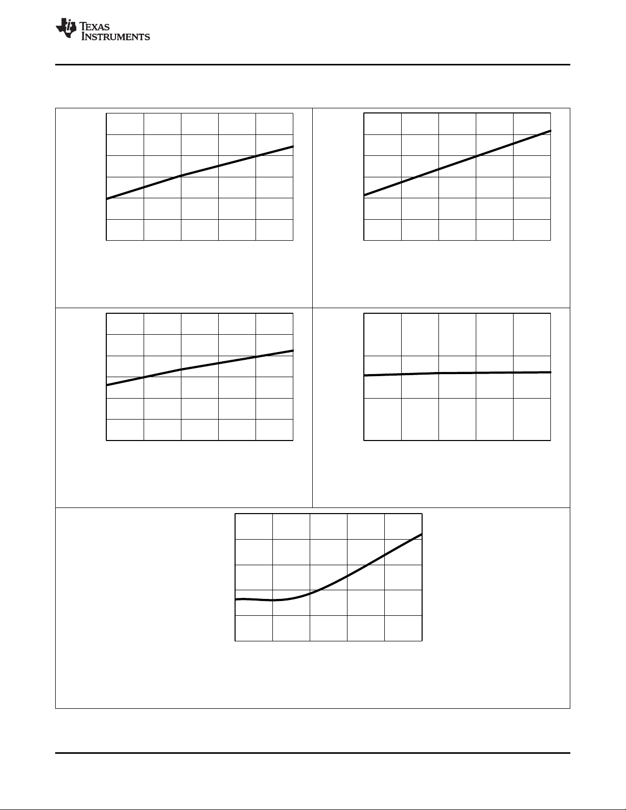
Figure 62. AVDD Current vs Temperature for the ADS8678 Figure 63. AVDD Current vs Temperature for the ADS8674
(During Sampling) (fS= 500 kSPS)
Figure 64. AVDD Current vs Temperature for the ADS8674 Figure 65. AVDD Current vs Temperature
(During Sampling) (STANDBY)
Figure 66. AVDD Current vs Temperature
(Power Down)
Copyright © 2015, Texas Instruments Incorporated Submit Documentation Feedback 21
Product Folder Links: ADS8674 ADS8678
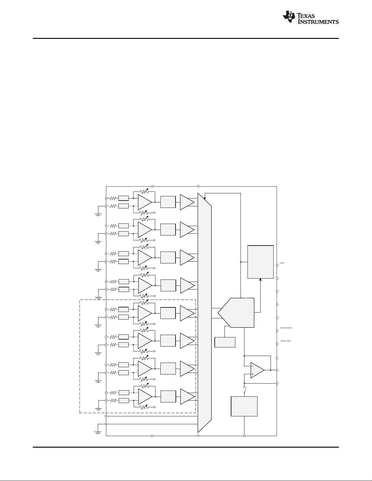
Multiplexer
Oscillator
PGA
1 M:
OVP
1 M:
2nd-Order
LPF
ADC
Driver
V
B0
AIN_0P
AIN_0GND
OVP
PGA
1 M:
OVP
1 M:
2nd-Order
LPF
ADC
Driver
V
B1
AIN_1P
AIN_1GND
OVP
PGA
1 M:
OVP
1 M:
2nd-Order
LPF
ADC
Driver
V
B2
AIN_2P
AIN_2GND
OVP
PGA
1 M:
OVP
1 M:
2nd-Order
LPF
ADC
Driver
V
B3
AIN_3P
AIN_3GND
OVP
PGA
1 M:
OVP
1 M:
2nd-Order
LPF
ADC
Driver
V
B4
AIN_4P
AIN_4GND
OVP
PGA
1 M:
OVP
1 M:
2nd-Order
LPF
ADC
Driver
V
B5
AIN_5P
AIN_5GND
OVP
PGA
1 M:
OVP
1 M:
2nd-Order
LPF
ADC
Driver
V
B6
AIN_6P
AIN_6GND
OVP
PGA
1 M:
OVP
1 M:
2nd-Order
LPF
ADC
Driver
V
B7
AIN_7P
AIN_7GND
OVP
AUX_IN
AUX_GND
14-Bit
SAR ADC
Digital
Logic
and
Interface
4.096-V
Reference
REFGND
DGNDAGND
DVDD
AVDD
Additional Channels in ADS8678
ADS8678
ADS8674
ALARM
CS
SCLK
SDI
SDO
DAISY
REFSEL
RST/PD
REFCAP
REFIO
ADS8674,ADS8678
SBAS627 –JULY 2015
www.ti.com
8 Detailed Description
8.1 Overview
The ADS8674 and ADS8678 are 14-bit data acquisition systems with 4- and 8-channel analog inputs,
respectively. Each analog input channel consists of an overvoltage protection circuit, a programmable gain
amplifier (PGA), and a second-order, antialiasing filter that conditions the input signal before being fed into a 4or 8-channel analog multiplexer (MUX). The output of the MUX is digitized using a 14-bit analog-to-digital
converter (ADC), based on the successive approximation register (SAR) architecture. This overall system can
achieve a maximum throughput of 500 kSPS, combined across all channels. The devices feature a 4.096-V
internal reference with a fast-settling buffer and a simple SPI-compatible serial interface with daisy-chain (DAISY)
and ALARM features.
The devices operate from a single 5-V analog supply and can accommodate true bipolar input signals up to
±2.5 × V
or the selected input range. The integration of multichannel precision analog front-end circuits with high input
impedance and a precision ADC operating from a single 5-V supply offers a simplified end solution without
requiring external high-voltage bipolar supplies and complicated driver circuits.
8.2 Functional Block Diagram
. The devices offer a constant 1-MΩ resistive input impedance irrespective of the sampling frequency
REF
22 Submit Documentation Feedback Copyright © 2015, Texas Instruments Incorporated
Product Folder Links: ADS8674 ADS8678
MUX
PGA
1 M:
OVP
1 M:
OVP
2nd-Order
LPF
ADC
Driver
V
B
ADC
AIN_nP
AIN_nGND
CS
SCLK
SDI
SDO
DAISY
ADS8674,ADS8678
www.ti.com
SBAS627 –JULY 2015
8.3 Feature Description
8.3.1 Analog Inputs
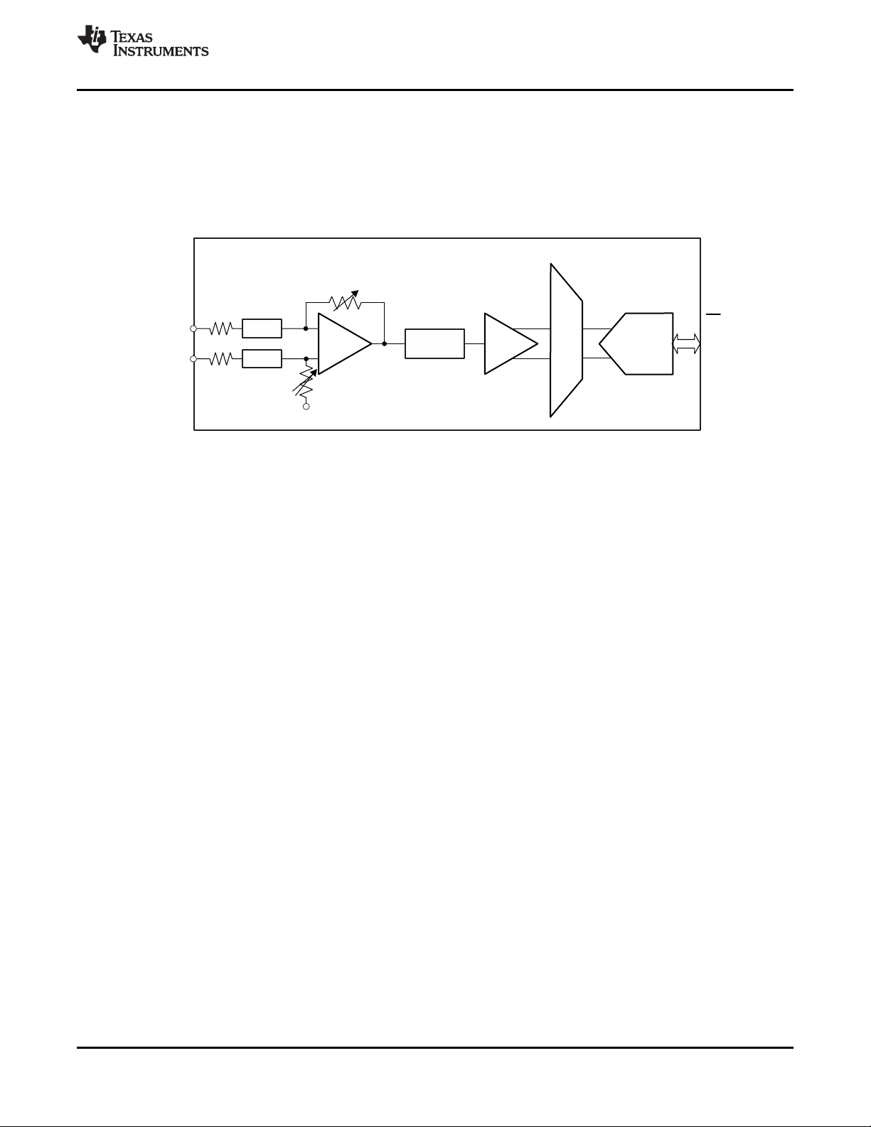
The ADS8674 and ADS8678 have either four or eight analog input channels, respectively, such that the positive
inputs AIN_nP (n = 0 to 3 or 7) are the single-ended analog inputs and the negative inputs AIN_nGND are tied to
GND. Figure 67 shows the simplified circuit schematic for each analog input channel, including the input
overvoltage protection circuit, PGA, low-pass filter (LPF), high-speed ADC driver, and analog multiplexer.
NOTE: n = 0 to 3 for the ADS8674 and n = 0 to 7 for the ADS8678.
Figure 67. Front-End Circuit Schematic for Each Analog Input Channel
The devices can support multiple unipolar or bipolar, single-ended input voltage ranges based on the
configuration of the program registers. As explained in the Range Select Registers section, the input voltage
range for each analog channel can be configured to bipolar ±2.5 × V
V
, and ±0.15625 × V
REF
V
. With the internal or external reference voltage set to 4.096 V, the input ranges of the device can be
REF
or unipolar 0 to 2.5 × V
REF
, 0 to 1.25 × V
REF
, ±1.25 × V
REF
, 0 to 0.625 × V
REF
, ±0.625 × V
REF
, ±0.3125 ×
REF
, and 0 to 0.3125 ×
REF
configured to bipolar ranges of ±10.24 V, ±5.12 V, ±2.56 V, ±1.28 V, and ±0.64 V or unipolar ranges of 0 V to
10.24 V, 0 V to 5.12 V, 0 V to 2.56 V, and 0 V to 1.28 V. Any of these input ranges can be assigned to any
analog input channel of the device. For instance, the ±2.5 × V
V
range can be assigned to AIN_2P, the 0 V to 2.5 × V
REF
REF
range can be assigned to AIN_1P, the ±1.25 ×
REF
range can be assigned to AIN_3P, and so forth.
The devices sample the voltage difference (AIN_nP – AIN_nGND) between the selected analog input channel
and the AIN_nGND pin. The devices allow a ±0.1-V range on the AIN_nGND pin for all analog input channels.
This feature is useful in modular systems where the sensor or signal-conditioning block is further away from the
ADC on the board and when a difference in the ground potential of the sensor or signal conditioner from the ADC
ground is possible. In such cases, running separate wires from the AIN_nGND pin of the device to the sensor or
signal-conditioning ground is recommended.
If the analog input pins (AIN_nP) to the devices are left floating, the output of the ADC corresponds to an internal
biasing voltage. The output from the ADC must be considered as invalid if the devices are operated with floating
input pins. This condition does not cause any damage to the devices, which are fully functional when a valid
input voltage is applied to the pins.
8.3.2 Analog Input Impedance
Each analog input channel in the device presents a constant resistive impedance of 1 MΩ. The input impedance
is independent of either the ADC sampling frequency, the input signal frequency, or range. The primary
advantage of such high-impedance inputs is the ease of driving the ADC inputs without requiring driving
amplifiers with low output impedance. Bipolar, high-voltage power supplies are not required in the system
because this ADC does not require any high-voltage front-end drivers. In most applications, the signal sources or
sensor outputs can be directly connected to the ADC input, thus significantly simplifying the design of the signal
chain.
In order to maintain the dc accuracy of the system, matching the external source impedance on the AIN_nP input
pin with an equivalent resistance on the AIN_nGND pin is recommended. This matching helps to cancel any
additional offset error contributed by the external resistance.
Copyright © 2015, Texas Instruments Incorporated Submit Documentation Feedback 23
Product Folder Links: ADS8674 ADS8678
V
OUT
V
+
V
±
+
V
B
AVDD
GND
AIN_nP
AIN_nGND
10
10
R
DC
R
FB
0V
V
P+
V
P-
R
S
ESD
D1p
D2n
R
S
AVDD
AVDD
D2p
D1n
ESD
ADS8674,ADS8678
SBAS627 –JULY 2015
www.ti.com
Feature Description (continued)
8.3.3 Input Overvoltage Protection Circuit
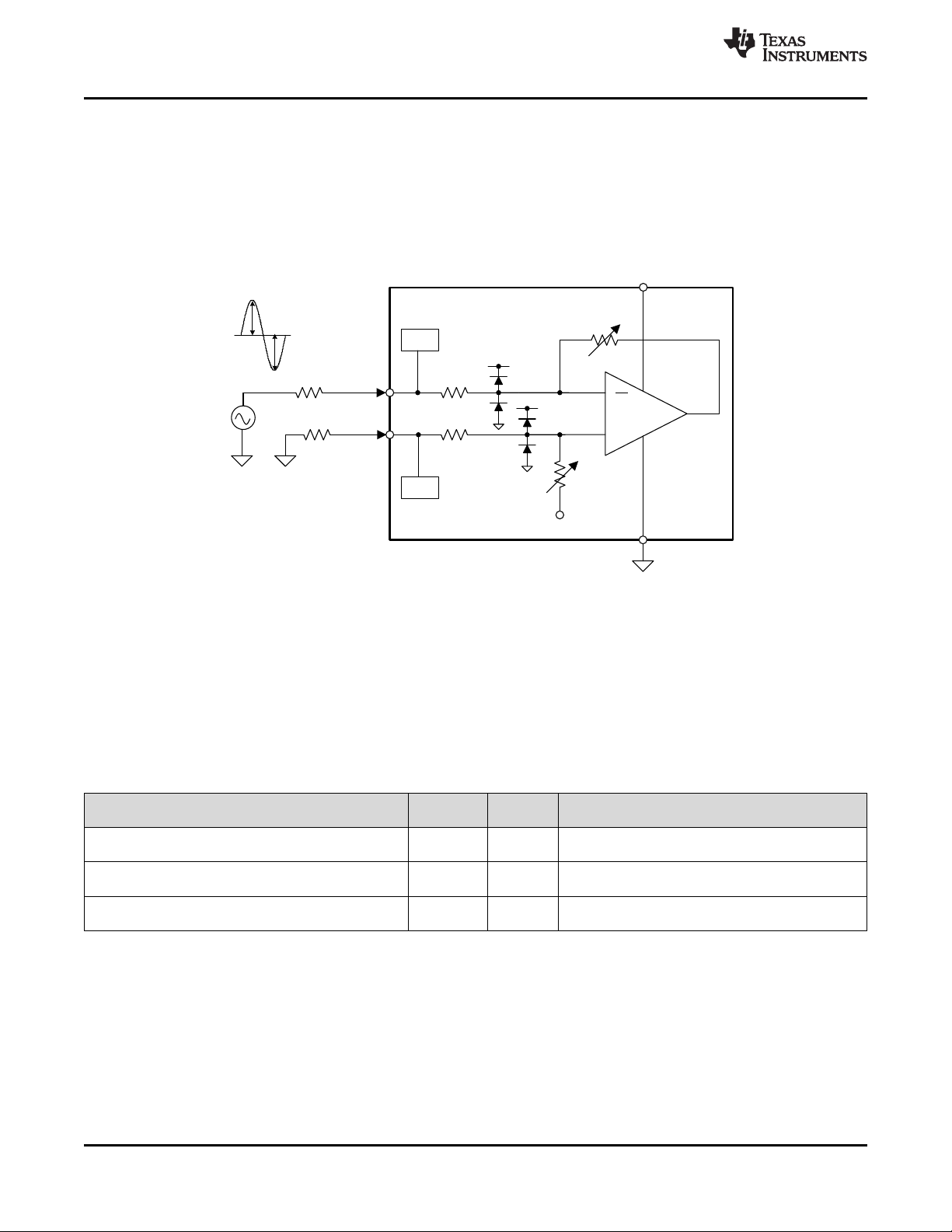
The ADS8674 and ADS8678 feature an internal overvoltage protection circuit on each of the four or eight analog
input channels, respectively. Use these protection circuits as a secondary protection scheme to protect the
device. Using external protection devices against surges, electrostatic discharge (ESD), and electrical fast
transient (EFT) conditions is highly recommended. The conceptual block diagram of the internal overvoltage
protection (OVP) circuit is shown in Figure 68.
Figure 68. Input Overvoltage Protection Circuit Schematic
As shown in Figure 68, the combination of the 1-MΩ input resistors along with the PGA gain-setting resistors
(RFBand RDC) limit the current flowing into the input pins. A combination of antiparallel diodes (D1 and D2) are
added on each input pin to protect the internal circuitry and set the overvoltage protection limits.
Table 1 explains the various operating conditions for the device when the device is powered on. Table 1
indicates that when the AVDD pin of the device is connected to the proper supply voltage (AVDD = 5 V) or offers
a low impedance of < 30 kΩ, the internal overvoltage protection circuit can withstand up to ±20 V on the analog
input pins.
Table 1. Input Overvoltage Protection Limits When AVDD = 5 V or Offers a Low Impedance of < 30 kΩ
INPUT CONDITION TEST ADC
(V
= ±20 V) CONDITION OUTPUT
OVP
|VIN| < |V
|V
RANGE
|VIN| > |V
(1) GND = 0, AIN_nGND = 0 V, |V
for the internal OVP circuit. Assume that RSis approximately 0.
The results indicated in Table 1 are based on an assumption that the analog input pins are driven by very low
impedance sources (RSis approximately 0). However, if the sources driving the inputs have higher impedance,
the current flowing through the protection diodes reduces further, thereby increasing the OVP voltage range.
Note that higher source impedance results in gain errors and contributes to overall system noise performance.
| Within operating range Valid Device functions as per data sheet specifications
RANGE
| < |VIN| < |V
| Beyond overvoltage range Saturated
OVP
Beyond operating range but All input ADC output is saturated, but device is internally
| Saturated
OVP
within overvoltage range ranges protected (not recommended for extended time)
| is the maximum input voltage for any selected input range, and |V
RANGE
All input
ranges
All input This usage condition may cause irreversible damage
ranges to the device
COMMENTS
| is the break-down voltage
OVP
(1)
24 Submit Documentation Feedback Copyright © 2015, Texas Instruments Incorporated
Product Folder Links: ADS8674 ADS8678
 Loading...