

-0.05
-0.03
-0.01
0.01
0.03
0.05
±40 ±7
26 59 92 125
Gain (% FS)
Free-Air Temperature (oC)
C039
---- ± 2.5*V
REF,
---- 1.25*V
REF
---- 0.625*V
REF,
------0.3125*V
REF
-------0.156 V
REF,
---- + 2.5*V
REF
---- + 1.25*V
REF,
---- + 0.625*V
REF
---- + 0.3125*V
REF
Multiplexer
Oscillator
CS
SCLK
SDI
SDO
DAISY
REFSEL
RST/PD
REFCAP
REFIO
PGA
1 M:
OVP
1 M:
2nd-Order
LPF
ADC
Driver
V
B0
AIN_0P
AIN_0GND
OVP
PGA
1 M:
OVP
1 M:
2nd-Order
LPF
ADC
Driver
V
B1
AIN_1P
AIN_1GND
OVP
PGA
1 M:
OVP
1 M:
2nd-Order
LPF
ADC
Driver
V
B2
AIN_2P
AIN_2GND
OVP
PGA
1 M:
OVP
1 M:
2nd-Order
LPF
ADC
Driver
V
B3
AIN_3P
AIN_3GND
OVP
PGA
1 M:
OVP
1 M:
2nd-Order
LPF
ADC
Driver
V
B4
AIN_4P
AIN_4GND
OVP
PGA
1 M:
OVP
1 M:
2nd-Order
LPF
ADC
Driver
V
B5
AIN_5P
AIN_5GND
OVP
PGA
1 M:
OVP
1 M:
2nd-Order
LPF
ADC
Driver
V
B6
AIN_6P
AIN_6GND
OVP
PGA
1 M:
OVP
1 M:
2nd-Order
LPF
ADC
Driver
V
B7
AIN_7P
AIN_7GND
OVP
AUX_IN
AUX_GND
12-Bit
SAR ADC
Digital
Logic
and
Interface
4.096-V
Reference
REFGND
DGNDAGND
DVDD
AVDD
Additional Channels in ADS8668
ADS8668
ADS8664
ALARM
Product
Folder
Sample &
Buy
Technical
Documents
Tools &
Software
Support &
Community
Reference
Design
ADS866x 12-Bit, 500-kSPS, 4- and 8-Channel, Single-Supply, SAR ADCs with
Bipolar Input Ranges
1 Features 2 Applications
1
• 12-Bit ADCs with Integrated Analog Front-End
• 4-, 8-Channel MUX with Auto and Manual Scan • Protection Relays
• Channel-Independent Programmable Inputs: • PLC Analog Input Modules
– ±10.24 V, ±5.12 V, ±2.56 V, ±1.28 V, ±0.64 V
– 10.24 V, 5.12 V, 2.56 V, 1.28 V
• 5-V Analog Supply: 1.65-V to 5-V I/O Supply
• Constant Resistive Input Impedance: 1 MΩ
• Input Overvoltage Protection: Up to ±20 V
• On-Chip, 4.096-V Reference with Low Drift
• Excellent Performance:
– 500-kSPS Aggregate Throughput
– DNL: ±0.2 LSB; INL: ±0.2 LSB
– Low Drift for Gain Error and Offset
– SNR: 73.8 dB; THD: –95 dB
– Low Power: 65 mW
• AUX Input → Direct Connection to ADC Inputs
• ALARM → High and Low Thresholds per Channel
• SPI™-Compatible Interface with Daisy-Chain
• Industrial Temperature Range: –40°C to 125°C
• TSSOP-38 Package (9.7 mm × 4.4 mm)
Block Diagram
• Power Automation
3 Description
The ADS8664 and ADS8668 are 4- and 8-channel,
integrated data acquisition systems based on a 12-bit
successive approximation (SAR) analog-to-digital
converter (ADC), operating at a throughput of
500 kSPS. The devices feature integrated analog
front-end circuitry for each input channel with
overvoltage protection up to ±20 V, a 4- or 8-channel
multiplexer with automatic and manual scanning
modes, and an on-chip, 4.096-V reference with low
temperature drift. Operating on a single 5-V analog
supply, each input channel on the devices can
support true bipolar input ranges of ±10.24 V,
±5.12 V, ±2.56 V, ±1.28V and ±0.64V, as well as
unipolar input ranges of 0 V to 10.24 V, 0 V to 5.12 V,
0 V to 2.56 V and 0 V to 1.28 V. The gain of the
analog front-end for all input ranges is accurately
trimmed to ensure a high dc precision. The input
range selection is software-programmable and
independent for each channel. The devices offer a
1-MΩ constant resistive input impedance irrespective
of the selected input range.
The ADS8664 and ADS8668 offer a simple SPIcompatible serial interface to the digital host and also
support daisy-chaining of multiple devices. The digital
supply operates from 1.65 V to 5.25 V, enabling
direct interface to a wide range of host controllers.
ADS8664,ADS8668
SBAS492 –JULY 2015
1
Device Information
Gain Error versus Temperature
PART NUMBER PACKAGE BODY SIZE (NOM)
ADS866x TSSOP (38) 9.70 mm × 4.40 mm
(1) For all available packages, see the orderable addendum at
the end of the datasheet.
An IMPORTANT NOTICE at the end of this data sheet addresses availability, warranty, changes, use in safety-critical applications,
intellectual property matters and other important disclaimers. PRODUCTION DATA.
(1)

ADS8664,ADS8668
SBAS492 –JULY 2015
www.ti.com
Table of Contents
1 Features.................................................................. 1
2 Applications ........................................................... 1
3 Description ............................................................. 1
4 Revision History..................................................... 2
5 Device Comparison Table..................................... 3
6 Pin Configuration and Functions......................... 3
7 Specifications......................................................... 5
7.1 Absolute Maximum Ratings ...................................... 5
7.2 ESD Ratings.............................................................. 5
7.3 Recommended Operating Conditions....................... 5
7.4 Thermal Information.................................................. 5
7.5 Electrical Characteristics........................................... 6
7.6 Timing Requirements: Serial Interface.................... 10
7.7 Typical Characteristics............................................ 11
8 Detailed Description ............................................ 22
8.1 Overview ................................................................. 22
8.2 Functional Block Diagram....................................... 22
8.3 Feature Description................................................. 23
4 Revision History
DATE REVISION NOTES
July 2014 * Initial release.
8.4 Device Functional Modes........................................ 36
8.5 Register Maps......................................................... 49
9 Application and Implementation........................ 65
9.1 Application Information............................................ 65
9.2 Typical Applications ................................................ 65
10 Power-Supply Recommendations ..................... 68
11 Layout................................................................... 69
11.1 Layout Guidelines ................................................. 69
11.2 Layout Example .................................................... 70
12 Device and Documentation Support................. 71
12.1 Documentation Support ........................................ 71
12.2 Related Links ........................................................ 71
12.3 Community Resources.......................................... 71
12.4 Trademarks........................................................... 71
12.5 Electrostatic Discharge Caution............................ 71
12.6 Glossary................................................................ 71
13 Mechanical, Packaging, and Orderable
Information........................................................... 72
2 Submit Documentation Feedback Copyright © 2015, Texas Instruments Incorporated
Product Folder Links: ADS8664 ADS8668
1
2
3
4
5
6
7
8
30
29
28
27
26
25
24
CS
SCLK
SDO
ALARM
DVDD
DGND
AGND
AGND
SDI
RST/PD
DAISY
REFSEL
REFIO
REFGND
REFCAP
22
21
20
AVDD
AGND
AGND
AIN_5P
AIN_5GND
AIN_4P
AIN_4GND
9AVDD
AUX_IN
AUX_GND
AIN_6P
AIN_6GND
AIN_7P
AIN_7GND
10
11
12
13
14
15
23
AIN_3P
AIN_3GND
AIN_2P
AIN2_GND
AIN_0P
AIN_0GND
AIN_1P
AIN_1GND
16
17
18
19
31
32
33
34
35
36
37
38
AGND
ADS8668
1
2
3
4
5
6
7
8
30
29
28
27
26
25
24
CS
SCLK
SDO
ALARM
DVDD
DGND
AGND
AGND
SDI
RST/PD
DAISY
REFSEL
REFIO
REFGND
REFCAP
22
21
20
AVDD
AGND
AGND
NC
NC
NC
NC
9AVDD
AUX_IN
AUX_GND
NC
NC
NC
NC
10
11
12
13
14
15
23
AIN_3P
AIN_3GND
AIN_2P
AIN2_GND
AIN_0P
AIN_0GND
AIN_1P
AIN_1GND
16
17
18
19
31
32
33
34
35
36
37
38
AGND
ADS8664
www.ti.com
5 Device Comparison Table
PRODUCT RESOLUTION (Bits) CHANNELS SAMPLE RATE (kSPS)
ADS8664 12 4, single-ended 500
ADS8668 12 8, single-ended 500
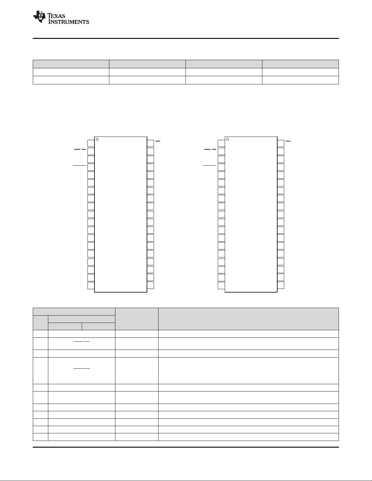
6 Pin Configuration and Functions
ADS8664,ADS8668
SBAS492 –JULY 2015
DBT Package
38-Pin TSSOP
Top View (Not to Scale)
Pin Functions
PIN
NO.
1 SDI Digital input Data input for serial communication.
2 RST/PD Digital input
3 DAISY Digital input Chain the data input during serial communication in daisy-chain mode.
4 REFSEL Digital input REFIO becomes an output that includes the V
5 REFIO Analog input, output Internal reference output and external reference input pin. Decouple with REFGND on pin 6.
6 REFGND Power supply
7 REFCAP Analog output ADC reference decoupling capacitor pin. Decouple with REFGND on pin 6.
8 AGND Power supply Analog ground pin. Decouple with AVDD on pin 9.
9 AVDD Power supply Analog supply pin. Decouple with AGND on pin 8.
10 AUX_IN Analog input Auxiliary input channel: positive input. Decouple with AUX_GND on pin 11.
11 AUX_GND Analog input Auxiliary input channel: negative input. Decouple with AUX_IN on pin 10.
Copyright © 2015, Texas Instruments Incorporated Submit Documentation Feedback 3
ADS8664 ADS8668
NAME I/O DESCRIPTION
Product Folder Links: ADS8664 ADS8668
Active low logic input.
Dual functionality to reset or power-down the device.
Active low logic input to enable the internal reference.
When low, the internal reference is enabled;
When high, the internal reference is disabled;
REFIO becomes an input to apply the external V
Reference GND pin; short to the analog GND plane.
Decouple with REFIO on pin 5 and REFCAP on pin 7.
REF
voltage.
REF
voltage.
ADS8664,ADS8668
SBAS492 –JULY 2015
Pin Functions (continued)
PIN
NO.
12 NC AIN_6P Analog input
13 NC AIN_6GND Analog input
14 NC AIN_7P Analog input
15 NC AIN_7GND Analog input
16 AIN_0P Analog input Analog input channel 0, positive input. Decouple with AIN_0GND on pin 17.
17 AIN_0GND Analog input Analog input channel 0, negative input. Decouple with AIN_0P on pin 16.
18 AIN_1P Analog input Analog input channel 1, positive input. Decouple with AIN_1GND on pin 19.
19 AIN_1GND Analog input Analog input channel 1, negative input. Decouple with AIN_1P on pin 18.
20 AIN2_GND Analog input Analog input channel 2, negative input. Decouple with AIN_2P on pin 21.
21 AIN_2P Analog input Analog input channel 2, positive input. Decouple with AIN_2GND on pin 20.
22 AIN_3GND Analog input Analog input channel 3, negative input. Decouple with AIN_3P on pin 23.
23 AIN_3P Analog input Analog input channel 3, positive input. Decouple with AIN_3GND on pin 22.
24 NC AIN_4GND Analog input
25 NC AIN_4P Analog input
26 NC AIN_5GND Analog input
27 NC AIN_5P Analog input
28 AGND Power supply Analog ground pin
29 AGND Power supply Analog ground pin
30 AVDD Power supply Analog supply pin. Decouple with AGND on pin 31.
31 AGND Power supply Analog ground pin. Decouple with AVDD on pin 30.
32 AGND Power supply Analog ground pin
33 DGND Power supply Digital ground pin. Decouple with DVDD on pin 34.
34 DVDD Power supply Digital supply pin. Decouple with DGND on pin 33.
35 ALARM Digital output Active high alarm output
36 SDO Digital output Data output for serial communication
37 SCLK Digital input Clock input for serial communication
38 CS Digital input Active low logic input; chip-select signal
ADS8664 ADS8668
NAME I/O DESCRIPTION
Analog input channel 6, positive input. Decouple with AIN_6GND on pin 13.
No connection for the ADS8664; this pin can be left floating or connected to AGND.
Analog input channel 6, negative input. Decouple with AIN_6P on pin 12.
No connection for the ADS8664; this pin can be left floating or connected to AGND.
Analog input channel 7, positive input. Decouple with AIN_7GND on pin 15.
No connection for the ADS8664; this pin can be left floating or connected to AGND.
Analog input channel 7, negative input. Decouple with AIN_7P on pin 14.
No connection for the ADS8664; this pin can be left floating or connected to AGND.
Analog input channel 4, negative input. Decouple with AIN_4P on pin 25.
No connection for the ADS8664; this pin can be left floating or connected to AGND.
Analog input channel 4, positive input. Decouple with AIN_4GND on pin 24.
No connection for the ADS8664; this pin can be left floating or connected to AGND.
Analog input channel 5, negative input. Decouple with AIN_5P on pin 27.
No connection for the ADS8664; this pin can be left floating or connected to AGND.
Analog input channel 5, positive input. Decouple with AIN_5GND on pin 26.
No connection for the ADS8664; this pin can be left floating or connected to AGND.
www.ti.com
4 Submit Documentation Feedback Copyright © 2015, Texas Instruments Incorporated
Product Folder Links: ADS8664 ADS8668
ADS8664,ADS8668
www.ti.com
SBAS492 –JULY 2015
7 Specifications
7.1 Absolute Maximum Ratings
over operating free-air temperature range (unless otherwise noted)
AIN_nP, AIN_nGND to GND
AIN_nP, AIN_nGND to GND
AUX_GND to GND –0.3 0.3 V
AUX_IN to GND –0.3 AVDD + 0.3 V
AVDD to GND or DVDD to GND –0.3 7 V
REFCAP to REFGND or REFIO to REFGND –0.3 5.7 V
GND to REFGND –0.3 0.3 V
Digital input pins to GND –0.3 DVDD + 0.3 V
Digital output pins to GND –0.3 DVDD + 0.3 V
Operating temperature, T
Storage temperature, T
(1) Stresses beyond those listed under Absolute Maximum Ratings may cause permanent damage to the device. These are stress ratings
only, and do not imply functional operation of the device at these or any other conditions beyond those indicated under Recommended
Operating Conditions. Exposure to absolute-maximum-rated conditions for extended periods may affect device reliability.
(2) AVDD = 5 V or offers a low impedance of < 30 kΩ.
(3) AVDD = floating with an impedance > 30 kΩ.
(2)
(3)
A
stg
(1)
MIN MAX UNIT
–20 20 V
–11 11 V
–40 125 °C
–65 150 °C
7.2 ESD Ratings
VALUE UNIT
V
Analog input pins
(1)
Electrostatic
(ESD)
discharge All other pins ±2000
Human body model (HBM), per ANSI/ESDA/JEDEC JS-001
Charged device model (CDM), per JEDEC specification JESD22-C101
(AIN_nP; AIN_nGND)
(2)
±4000
±500
(1) JEDEC document JEP155 states that 500-V HBM allows safe manufacturing with a standard ESD control process.
(2) JEDEC document JEP157 states that 250-V CDM allows safe manufacturing with a standard ESD control process.
7.3 Recommended Operating Conditions
over operating free-air temperature range (unless otherwise noted)
MIN NOM MAX UNIT
AVDD Analog supply voltage 4.75 5 5.25 V
DVDD Digital supply voltage 1.65 3.3 AVDD V
7.4 Thermal Information
ADS8664,
(1)
R
θJA
R
θJC(top)
R
θJB
ψ
JT
ψ
JB
R
θJC(bot)
THERMAL METRIC
Junction-to-ambient thermal resistance 68.8 °C/W
Junction-to-case (top) thermal resistance 19.9 °C/W
Junction-to-board thermal resistance 30.4 °C/W
Junction-to-top characterization parameter 1.3 °C/W
Junction-to-board characterization parameter 29.8 °C/W
Junction-to-case (bottom) thermal resistance NA °C/W
(1) For more information about traditional and new thermal metrics, see the IC Package Thermal Metrics application report, SPRA953.
ADS8668
DBT (TSSOP)
38 PINS
UNIT
V
Copyright © 2015, Texas Instruments Incorporated Submit Documentation Feedback 5
Product Folder Links: ADS8664 ADS8668
ADS8664,ADS8668
SBAS492 –JULY 2015
www.ti.com
7.5 Electrical Characteristics
Minimum and maximum specifications are at TA= –40°C to 125°C. Typical specifications are at TA= 25°C.
AVDD = 5 V, DVDD = 3 V, V
PARAMETER TEST CONDITIONS MIN TYP MAX UNIT
ANALOG INPUTS
Full-scale input span
(AIN_nP to AIN_nGND) Input range = ±0.15625 × V
AIN_nP –0.15625 × 0.15625 × V
AIN_nGND All input ranges –0.1 0 0.1 V B
z
i
I
Ikg(in)
INPUT OVERVOLTAGE PROTECTION
V
OVP
(1) Test Levels: (A) Tested at final test. Over temperature limits are set by characterization and simulation. (B) Limits set by characterization
and simulation, across temperature range. (C) Typical value only for information, provided by design simulation.
(2) Ideal input span, does not include gain or offset error.
Operating input range,
positive input Input range = ±0.15625 × V
Operating input range,
negative input
Input impedance 0.85 1 1.15 MΩ B
Input impedance drift All input ranges 7 25 ppm/°C B
Input leakage current input ranges = ±0.625 × V
Overvoltage protection voltage V
= 4.096 V (internal), and f
REF
Input range = ±2.5 × V
Input range = ±1.25 × V
Input range = ±0.625 × V
Input range = ±0.3125 × V
(2)
Input range = 2.5 × V
Input range = 1.25 × V
Input range = 0.625 × V
Input range = 0.3125 × V
Input range = ±2.5 × V
Input range = ±1.25 × V
Input range = ±0.625 × V
Input range = ±0.3125 × V
Input range = 2.5 × V
Input range = 1.25 × V
Input range = 0.625 × V
Input range = 0.3125 × V
At TA= 25°C,
all input ranges
With voltage at AIN_nP pin = VIN,
input range = ±2.5 × V
With voltage at AIN_nP pin = VIN,
input range = ±1.25 × V
With voltage at AIN_nP pin = VIN, VIN– 1.60
±0.3125 × V
With voltage at AIN_nP pin = VIN,
input range = 2.5 × V
With voltage at AIN_nP pin = VIN, VIN– 2.50
input range = 1.25 × V
V
; 0.3125 × V
REF
AVDD = 5 V or offers low
impedance < 30 kΩ, all input ranges
AVDD = floating with impedance
> 30 kΩ, all input ranges
SAMPLE
; ±0.15625 × V
REF
REF
= 500 kSPS, unless otherwise noted.
REF
REF
REF
REF
REF
REF
REF
REF
REF
REF
REF
REF
REF
REF
REF
REF
REF
REF
–2.5 × V
REF
–1.25 × V
–0.625 × V
REF
REF
–0.3125 ×
V
REF
–0.15625 × 0.15625 × V
V
REF
0 2.5 × V
0 1.25 × V
0 0.625 × V
0 0.3125 × V
–2.5 × V
REF
–1.25 × V
–0.625 × V
REF
REF
–0.3125 ×
V
REF
V
REF
0 2.5 × V
0 1.25 × V
0 0.625 × V
0 0.3125 × V
VIN– 2.25
REF
———— A
R
IN
VIN– 2.00
REF
; ———— µA A
REF
REF
———— A
R
IN
R
IN
VIN– 2.50
REF
; 0.625 × ———— A
REF
———— A
R
IN
R
IN
–20 20 B
–11 11 B
2.5 × V
1.25 × V
0.625 × V
0.3125 × V
2.5 × V
1.25 × V
0.625 × V
0.3125 × V
REF
REF
REF
REF
V
REF
REF
REF
REF
REF
REF
REF
REF
REF
V
REF
REF
REF
REF
REF
TEST
LEVEL
A
A
A
A
A
A
A
A
A
A
A
A
A
A
A
A
A
A
(1)
6 Submit Documentation Feedback Copyright © 2015, Texas Instruments Incorporated
Product Folder Links: ADS8664 ADS8668
ADS8664,ADS8668
www.ti.com
SBAS492 –JULY 2015
Electrical Characteristics (continued)
Minimum and maximum specifications are at TA= –40°C to 125°C. Typical specifications are at TA= 25°C.
AVDD = 5 V, DVDD = 3 V, V
PARAMETER TEST CONDITIONS MIN TYP MAX UNIT
SYSTEM PERFORMANCE
Resolution 12 Bits A
NMC No missing codes 12 Bits A
DNL Differential nonlinearity –0.5 ±0.2 0.5 LSB
INL Integral nonlinearity
E
G
E
O
SAMPLING DYNAMICS
t
CONV
t
ACQ
f
S
(3) LSB = least significant bit.
(4) This parameter is the endpoint INL, not best-fit INL.
(5) FSR = full-scale range.
Gain error At TA= 25°C, all input ranges ±0.05 ±0.1 %FSR
Gain error matching
(channel-to-channel)
Gain error temperature drift All input ranges 1 5 ppm/°C B
Offset error ±1 ±2.5 mV A
Offset error matching At TA= 25°C,
(channel-to-channel) all input ranges
Offset error temperature drift Input range = ±0.15625 × V
Conversion time 850 ns A
Acquisition time 1150 ns A
Maximum throughput rate
without latency
= 4.096 V (internal), and f
REF
(4)
At TA= 25°C, all input ranges ±0.05 ±0.1 %FSR A
At TA= 25°C,
all input ranges
Input range = ±2.5 × V
Input range = ±1.25 × V
Input range = ±0.625 × V
Input range = ±0.3125 × V
Input range = 0 to 2.5 × V
Input range = 0 to 1.25 × V
Input range = 0 to 0.625 × V
Input range = 0 to 0.3125 × V
= 500 kSPS, unless otherwise noted.
SAMPLE
–0.5 ±0.2 0.5 LSB A
REF
REF
REF
REF
REF
REF
REF
REF
REF
LEVEL
(3)
(5)
±1 ±2.5 mV A
1 3 B
1 3 B
1 3 B
2 6 B
4 12 ppm/°C B
1 3 B
1 3 B
2 6 B
4 12 B
500 kSPS A
TEST
A
A
(1)
Copyright © 2015, Texas Instruments Incorporated Submit Documentation Feedback 7
Product Folder Links: ADS8664 ADS8668
ADS8664,ADS8668
SBAS492 –JULY 2015
www.ti.com
Electrical Characteristics (continued)
Minimum and maximum specifications are at TA= –40°C to 125°C. Typical specifications are at TA= 25°C.
AVDD = 5 V, DVDD = 3 V, V
PARAMETER TEST CONDITIONS MIN TYP MAX UNIT
DYNAMIC CHARACTERISTICS
SNR Input range = ±0.15625 × V
THD All input ranges –95 dB B
SINAD Input range = ±0.15625 × V
SFDR All input ranges 97 dB B
BW
(–3 dB)
BW
(–0.1 dB)
AUXILIARY CHANNEL
V
(AUX_IN)
C
i
I
Ikg(in)
DNL Differential nonlinearity –0.5 ±0.2 0.5 LSB A
INL Integral nonlinearity –0.75 ±0.5 0.75 LSB A
E
G(AUX)
E
O(AUX)
SNR Signal-to-noise ratio V
THD Total harmonic distortion
SINAD Signal-to-noise + distortion V
SFDR Spurious-free dynamic range V
(6) Calculated on the first nine harmonics of the input frequency.
(7) Isolation crosstalk is measured by applying a full-scale sinusoidal signal up to 10 kHz to a channel, not selected in the multiplexing
sequence, and measuring its effect on the output of any selected channel.
(8) Memory crosstalk is measured by applying a full-scale sinusoidal signal up to 10 kHz to a channel that is selected in the multiplexing
sequence, and measuring its effect on the output of the next selected channel for all combinations of input channels.
Signal-to-noise ratio
(VIN– 0.5 dBFS at 1 kHz)
Total harmonic distortion
(VIN– 0.5 dBFS at 1 kHz)
Signal-to-noise ratio
(VIN– 0.5 dBFS at 1 kHz)
Spurious-free dynamic range
(VIN– 0.5 dBFS at 1 kHz)
Crosstalk isolation
Crosstalk memory
Small-signal bandwidth, –3 dB At TA= 25°C, all input ranges 15 kHz B
Small-signal bandwidth, –0.1 dB At TA= 25°C, all input ranges 2.5 kHz B
Resolution 12 Bits A
AUX_IN voltage range (AUX_IN – AUX_GND) 0 V
Operating input range
Input capacitance
Input leakage current 100 nA A
Gain error At TA= 25°C ±0.02 ±0.2 %FSR A
Offset error At TA= 25°C –5 5 mV A
= 4.096 V (internal), and f
REF
Input range = ±2.5 × V
Input range = ±1.25 × V
Input range = ±0.625 × V
Input range = ±0.3125 × V
Input range = 2.5 × V
Input range = 1.25 × V
Input range = 0.625 × V
Input range = 0.3125 × V
(6)
Input range = ±2.5 × V
Input range = ±1.25 × V
Input range = ±0.625 × V
Input range = ±0.3125 × V
Input range = 2.5 × V
Input range = 1.25 × V
Input range = 0.625 × V
Input range = 0.3125 × V
(7)
(8)
Aggressor channel input overdriven
to 2 × maximum input voltage
Aggressor channel input overdriven
to 2 × maximum input voltage
AUX_IN 0 V
AUX_GND 0 V A
During sampling 75 pF C
During conversion 5 pF C
(6)
(AUX_IN)
V
(AUX_IN)
(AUX_IN)
(AUX_IN)
= 500 kSPS, unless otherwise noted.
SAMPLE
TEST
LEVEL
REF
REF
REF
REF
REF
REF
REF
REF
REF
REF
REF
REF
REF
REF
REF
REF
REF
REF
73 73.85 A
73 73.85 A
73 73.85 A
72.7 73.5 A
71.4 72.5 dB A
73 73.85 A
73 73.85 A
72.7 73.5 A
71.4 72.5 A
73 73.8 A
73 73.8 A
73 73.8 A
72.7 73.5 A
71.4 72.5 dB A
73 73.8 A
73 73.8 A
72.7 73.5 A
71.4 72.5 A
110 dB B
90 dB B
V A
REF
V A
REF
= –0.5 dBFS at 1 kHz 73.2 73.7 dB A
= –0.5 dBFS at 1 kHz –90 dB B
= –0.5 dBFS at 1 kHz 72.5 73.5 dB A
= –0.5 dBFS at 1 kHz 93 dB B
(1)
8 Submit Documentation Feedback Copyright © 2015, Texas Instruments Incorporated
Product Folder Links: ADS8664 ADS8668
ADS8664,ADS8668
www.ti.com
SBAS492 –JULY 2015
Electrical Characteristics (continued)
Minimum and maximum specifications are at TA= –40°C to 125°C. Typical specifications are at TA= 25°C.
AVDD = 5 V, DVDD = 3 V, V
PARAMETER TEST CONDITIONS MIN TYP MAX UNIT
INTERNAL REFERENCE OUTPUT
Voltage on REFIO pin
(REFIO_INT)
(OUT_REFIO)
(REFCAP)
(OUT_REFCAP)
REFIO_EXT
IH
IL
IH
IL
OH
OL
A
(9)
(configured as output)
Internal reference temperature
drift
Decoupling capacitor on REFIO 10 22 µF B
Reference voltage to ADC
(on REFCAP pin)
Reference buffer output
impedance
Reference buffer temperature
drift
Decoupling capacitor on
REFCAP
Turn-on time 15 ms B
External reference voltage on
REFIO (configured as input)
Analog supply current Static mA
Digital supply current At DVDD = 3.3 V, output = 0000h 0.5 mA A
Digital input logic levels
DVDD > 2.1 V
Digital input logic levels
DVDD ≤ 2.1 V
Input leakage current 100 nA A
Input pin capacitance 5 pF C
Digital output logic levels V
Floating state leakage current Only for SDO 1 µA A
Internal pin capacitance 5 pF C
Operating free-air temperature –40 125 °C B
V
C
V
C
EXTERNAL REFERENCE INPUT
V
POWER-SUPPLY REQUIREMENTS
AVDD Analog power-supply voltage Analog supply 4.75 5 5.25 V B
DVDD Digital power-supply voltage V
I
AVDD_DYN
I
AVDD_STC
I
STDBY
I
PWR_DN
I
DVDD_DYN
DIGITAL INPUTS (CMOS)
V
V
V
V
DIGITAL OUTPUTS (CMOS)
V
V
TEMPERATURE RANGE
T
(9) Does not include the variation in voltage resulting from solder-shift and long-term effects.
= 4.096 V (internal), and f
REF
= 500 kSPS, unless otherwise noted.
SAMPLE
At TA= 25°C 4.094 4.096 4.098 V A
8 20 ppm/°C B
At TA= 25°C 4.094 4.096 4.098 V A
0.5 1 Ω B
0.6 1.5 ppm/°C B
10 22 μF B
C
(OUT_REFCAP)
C
(OUT_REFIO)
= 22 µF,
= 22 µF
4.046 4.096 4.146 V C
Digital supply range 1.65 3.3 AVDD B
Dynamic,
AVDD
Digital supply range for specified
performance
For the ADS8668; AVDD = 5 V, fS=
maximum and internal reference
For the ADS8664; AVDD = 5 V, fS=
maximum and internal reference
2.7 3.3 5.25 B
13 16 A
8.5 11.5 A
For the ADS8668; AVDD = 5 V,
device not converting and internal 10 12 A
reference
For the ADS8664; AVDD = 5 V,
device not converting and internal 5.5 8.5 A
reference
Standby 3 4.5 mA A
Power-
down
At AVDD = 5 V, device in STDBY
mode and internal reference
At AVDD = 5 V, device in PWR_DN 3 20 μA B
0.7 × DVDD DVDD + 0.3 A
–0.3 0.3 × DVDD A
0.8 × DVDD DVDD + 0.3 A
–0.3 0.2 × DVDD A
IO= 500-μA source 0.8 × DVDD DVDD A
IO= 500-μA sink 0 0.2 × DVDD A
LEVEL
mA
V
V
TEST
(1)
Copyright © 2015, Texas Instruments Incorporated Submit Documentation Feedback 9
Product Folder Links: ADS8664 ADS8668
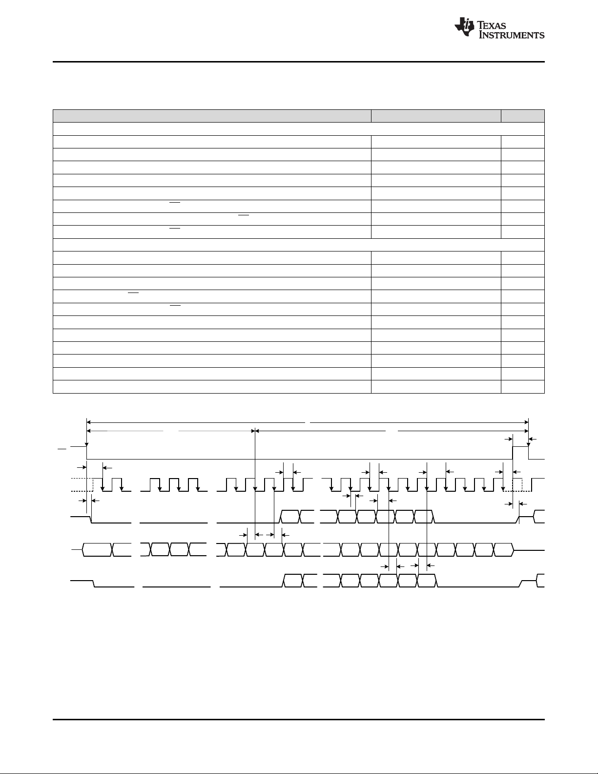
1 2 14 15 16 17
23 24
25
26
27 28 29
30SCLK
CS
D5#2D4#2D3
#2
D2#2D1
#2
D0
#2
SDO
t
SU_CSCK
t
DV_CSDO
t
HT_CKDO
t
SU_DOCK
t
DZ_CSDO
Sample
N
Sample
N + 1
t
ACQ
t
CONV
t
S
Data from sample N
t
PH_CS
31 32
D11
#2
D10
#2
18
B15
B14 B2
B1 B0 X X
X X X X
SDI
X
X X X X X
t
PH_CK
t
PL_CK
t
SCLK
t
SU_DICK
t
HT_CKDI
t
D_CKCS
7 8 9
B9 B8 B7B10
B3
D5#1D4#1D3
#1
D2#1D1
#1
D0
#1
DAISY
D11
#1
D10
#1
t
HT_CKDSY
t
SU_DSYCK
ADS8664,ADS8668
SBAS492 –JULY 2015
7.6 Timing Requirements: Serial Interface
Minimum and maximum specifications are at TA= –40°C to 125°C. Typical specifications are at TA= 25°C.
AVDD = 5 V, DVDD = 3 V, V
TIMING SPECIFICATIONS
f
S
t
S
f
SCLK
t
SCLK
t
CONV
t
DZ_CSDO
t
D_CKCS
t
DZ_CSDO
TIMING REQUIREMENTS
t
ACQ
t
PH_CK
t
PL_CK
t
PH_CS
t
SU_CSCK
t
HT_CKDO
t
SU_DOCK
t
SU_DICK
t
HT_CKDI
t
SU_DSYCK
t
HT_CKDSY
Sampling frequency (f
ADC cycle time period (f
Serial clock frequency (fS= max) 17 MHz
Serial clock time period (fS= max) 59 ns
Conversion time 850 ns
Delay time: CS falling to data enable 10 ns
Delay time: last SCLK falling to CS rising 10 ns
Delay time: CS rising to SDO going to 3-state 10 ns
Acquisition time 1150 ns
Clock high time 0.4 0.6 t
Clock low time 0.4 0.6 t
CS high time 30 ns
Setup time: CS falling to SCLK falling 30 ns
Hold time: SCLK falling to (previous) data valid on SDO 10 ns
Setup time: SDO data valid to SCLK falling 25 ns
Setup time: SDI data valid to SCLK falling 5 ns
Hold time: SCLK falling to (previous) data valid on SDI 5 ns
Setup time: DAISY data valid to SCLK falling 5 ns
Hold time: SCLK falling to (previous) data valid on DAISY 5 ns
= 4.096 V (internal), SDO load = 20 pF, and f
REF
= max) 500 kSPS
CLK
= max) 2 µs
CLK
= 500 kSPS, unless otherwise noted.
SAMPLE
MIN TYP MAX UNIT
www.ti.com
SCLK
SCLK
10 Submit Documentation Feedback Copyright © 2015, Texas Instruments Incorporated
Figure 1. Serial Interface Timing Diagram
Product Folder Links: ADS8664 ADS8668
0
500
1000
1500
2000
2500
3000
2045 2046 2047 2048 2049 2050 2051
Number of Hits
Output Codes
C007
0
500
1000
1500
2000
2500
3000
2045 2046 2047 2048 2049 2050 2051
Number of Hits
Output Codes
C008
0
160
320
480
640
800
0.85 0.88 0.91 0.94 0.97 1 1.03 1.06 1.09 1.12 1.15
Njumber of Samples
Input Impedance (M)
C006
-70
0
70
140
210
280
350
±40 ±7
26 59 92 125
Input Impedance Variation ()
Free-Air Temperature (oC)
C005
---- ± 2.5*V
REF,
---- 1.25*V
REF
---- 0.625*V
REF,
------0.3125*V
REF
-------0.156 V
REF,
---- + 2.5*V
REF
---- + 1.25*V
REF,
---- + 0.625*V
REF
---- + 0.3125*V
REF
±15
±9
±3
3
9
15
±10 ±6 ±2
2 6 10
Analog Input Current (µA)
Input Voltage (V)
C001
---- ± 2.5*V
REF,
---- 1.25*V
REF
---- 0.625*V
REF,
------0.3125*V
REF
-------0.156 V
REF,
---- + 2.5*V
REF
---- + 1.25*V
REF,
---- + 0.625*V
REF
---- + 0.3125*V
REF
±15
±9
±3
3
9
15
±10 ±6 ±2
2 6 10
Analog Input Current (µA)
Input Voltage (V)
C002
----- -400C
----- 250C
----- 1250C
www.ti.com
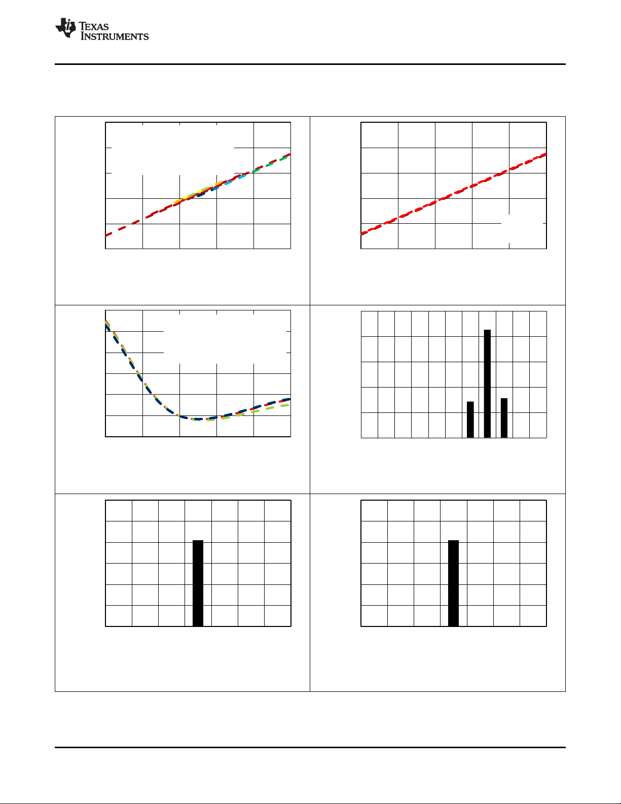
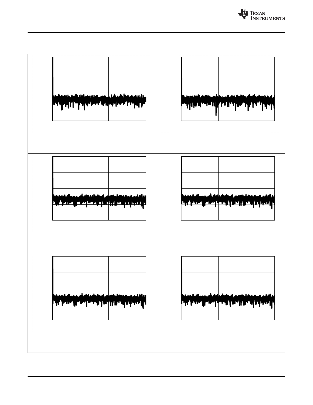
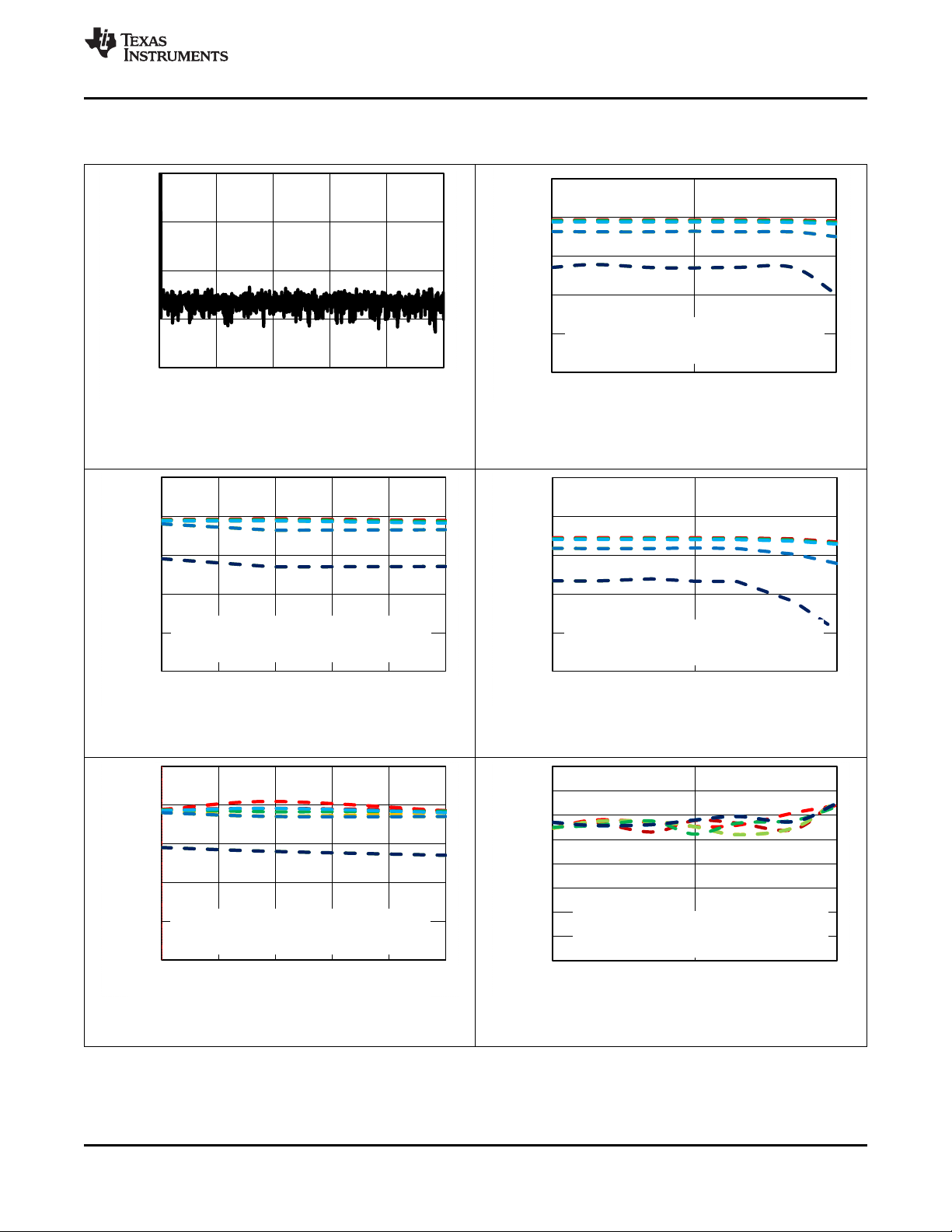
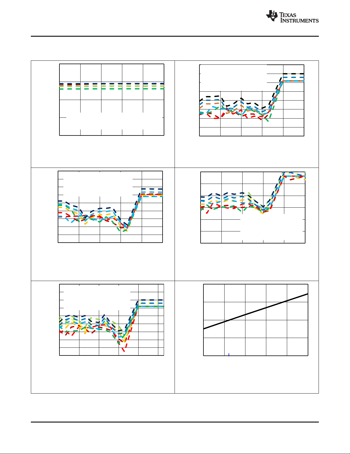
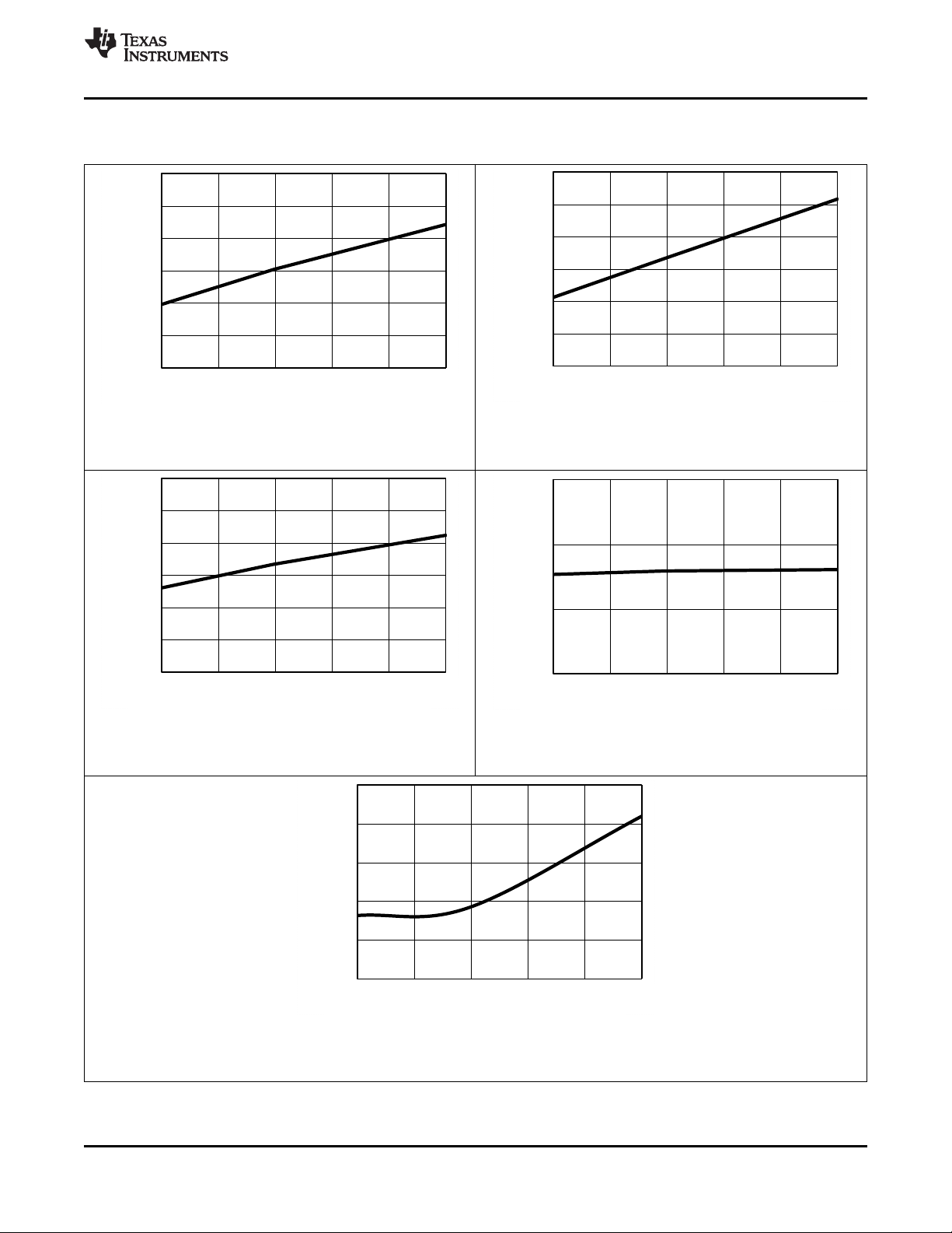
7.7 Typical Characteristics
At TA= 25°C, AVDD = 5 V, DVDD = 3 V, internal reference V
= 4.096 V, and f
REF
ADS8664,ADS8668
SBAS492 –JULY 2015
= 500 kSPS, unless otherwise noted.
SAMPLE
Figure 2. Input I-V Characteristic Figure 3. Input Current vs Temperature
Figure 4. Input Impedance Variation vs Temperature
Input range = ±2.5 × V
REF
Number of samples = 1160
Figure 5. Typical Distribution of Input Impedance
Figure 6. DC Histogram for Mid-Scale Inputs (±2.5 × V
Mean = 2048, sigma = 0.0, input = 0 V, Mean = 2048, sigma = 0.0, input = 0 V,
range = ±2.5 × V
Copyright © 2015, Texas Instruments Incorporated Submit Documentation Feedback 11
REF
) Figure 7. DC Histogram for Mid-Scale Inputs (±1.25 × V
REF
Product Folder Links: ADS8664 ADS8668
range = ±1.25 × V
REF
REF
)
0
1000
2000
3000
2044 2045 2046 2047 2048 2049 2050 2051
Number of Hits
Output Codes
C013
0
1000
2000
3000
2045 2046 2047 2048 2049 2050 2051
Number of Hits
Output Codes
C014
0
1000
2000
3000
2044 2046 2048 2050 2052
Number of Hits
Output Codes
C011
0
1000
2000
3000
2045 2046 2047 2048 2049 2050
Number of Hits
Output Codes
C012
0
500
1000
1500
2000
2044 2045 2046 2047 2048 2049 2050 2051 2052
Number of Hits
Output Codes
C009
0
1000
2000
3000
2044 2045 2046 2047 2048 2049 2050 2051 2052
Number of Hits
Output Codes
C010
ADS8664,ADS8668
SBAS492 –JULY 2015
Typical Characteristics (continued)
www.ti.com
At TA= 25°C, AVDD = 5 V, DVDD = 3 V, internal reference V
Mean = 2048, sigma = 0.1, input = 0 V, Mean = 2048, sigma = 0.0, input = 1.25 × V
range = ±0.625 × V
Figure 8. DC Histogram for Mid-Scale Inputs (±0.625 × V
REF
REF
= 4.096 V, and f
REF
= 500 kSPS, unless otherwise noted.
SAMPLE
range = 2.5 × V
REF
REF
,
) Figure 9. DC Histogram for Mid-Scale Inputs (2.5 × V
REF
)
Mean = 2048, sigma = 0.0, input = 0.625 × V
range = 1.25 × V
Figure 10. DC Histogram for Mid-Scale Inputs Figure 11. DC Histogram for Mid-Scale Inputs
Mean = 2048, sigma = 0.18, input = 0 V, Mean = 2048, sigma = 0.1, input = 0.3125 × V
12 Submit Documentation Feedback Copyright © 2015, Texas Instruments Incorporated
Figure 12. DC Histogram for Mid-Scale Inputs Figure 13. DC Histogram for Mid-Scale Inputs
range = ±0.15625 × V
(1.25 × V
REF
(±0.15625 x V
, Mean = 2048, sigma = 0.1, input = 0 V,
REF
REF
range = ±0.3125 × V
) (±0.3125 x V
REF
) (0.625 x V
REF
range = 0.625 × V
Product Folder Links: ADS8664 ADS8668
REF
REF
REF
REF
)
)
,
REF
-0.5
-0.3
-0.1
0.1
0.3
0.5
0 1024 2048 3072 4096
Integral Nonlinearity (LSB)
Codes (LSB)
C019
-0.5
-0.3
-0.1
0.1
0.3
0.5
0 1024 2048 3072 4096
Integral Nonlinearity (LSB)
Codes (LSB)
C020
-0.5
-0.25
0
0.25
0.5
0 1024 2048 3072 4096
Integral Nonlinearity (LSB)
Codes (LSB)
C018
-0.5
-0.3
-0.1
0.1
0.3
0.5
±40 ±7
26 59 92 125
Differential Nonlinearity (LSB)
Free-Air Temperature (oC)
C017
Maximum
Minimum
0
1000
2000
3000
2045 2046 2047 2048 2049 2050 2051
Number of Hits
Output Codes
C015
-0.5
-0.4
-0.3
-0.2
-0.1
0
0.1
0.2
0.3
0.4
0.5
0 512 1024 1536 2048 2560 3072 3584 4096
Differential Nonlinearity (LSB)
Codes (LSB) C016
www.ti.com
Typical Characteristics (continued)
ADS8664,ADS8668
SBAS492 –JULY 2015
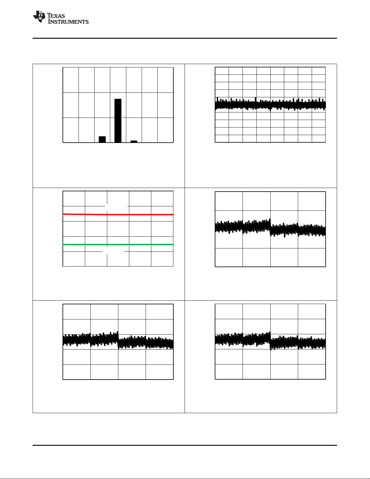
At TA= 25°C, AVDD = 5 V, DVDD = 3 V, internal reference V
Mean = 2048, sigma = 0.18, input = 0.15625 × V
range = 0.3125 × V
REF
Figure 14. DC Histogram for Mid-Scale Inputs
(0.3125 x V
REF
)
REF
,
= 4.096 V, and f
REF
= 500 kSPS, unless otherwise noted.
SAMPLE
All input ranges
Figure 15. Typical DNL for All Codes
All input ranges
Figure 16. DNL vs Temperature
Copyright © 2015, Texas Instruments Incorporated Submit Documentation Feedback 13
Range = ±1.25 × V
Figure 18. Typical INL for All Codes Figure 19. Typical INL for All Codes
REF
Product Folder Links: ADS8664 ADS8668
Range = ±2.5 × V
REF
Figure 17. Typical INL for All Codes
Range = ±0.625 × V
REF
-0.5
-0.3
-0.1
0.1
0.3
0.5
0 1024 2048 3072 4096
Integral Nonlinearity (LSB)
Codes (LSB)
C025
-0.5
-0.3
-0.1
0.1
0.3
0.5
0 1024 2048 3072 4096
Integral Nonlinearity (LSB)
Codes (LSB)
C026
-0.5
-0.3
-0.1
0.1
0.3
0.5
0 1024 2048 3072 4096
Integral Nonlinearity (LSB)
Codes (LSB)
C023
-0.5
-0.3
-0.1
0.1
0.3
0.5
0 1024 2048 3072 4096
Integral Nonlinearity (LSB)
Codes (LSB)
C024
-0.5
-0.3
-0.1
0.1
0.3
0.5
0 1024 2048 3072 4096
Integral Nonlinearity (LSB)
Codes (LSB)
C021
-0.5
-0.3
-0.1
0.1
0.3
0.5
0 1024 2048 3072 4096
Integral Nonlinearity (LSB)
Codes (LSB)
C022
ADS8664,ADS8668
SBAS492 –JULY 2015
Typical Characteristics (continued)
www.ti.com
At TA= 25°C, AVDD = 5 V, DVDD = 3 V, internal reference V
Range = 2.5 × V
Figure 20. Typical INL for All Codes Figure 21. Typical INL for All Codes
REF
= 4.096 V, and f
REF
= 500 kSPS, unless otherwise noted.
SAMPLE
Range = 1.25 × V
REF
Range = ±0.3125 × V
REF
Range = ±0.15625 × V
REF
Figure 22. Typical INL for All Codes Figure 23. Typical INL for All Codes
Range = 0.625 × V
REF
Range = 0.3125 × V
REF
Figure 24. Typical INL for All Codes Figure 25. Typical INL for All Codes
14 Submit Documentation Feedback Copyright © 2015, Texas Instruments Incorporated
Product Folder Links: ADS8664 ADS8668
-0.5
-0.25
0
0.25
0.5
±40 ±7
26 59 92 125
Integgral Nonlinearity (LSB)
Free-Air Temperature (oC)
C031
Minimum
Maximum
-0.5
-0.3
-0.1
0.1
0.3
0.5
±40 ±7
26 59 92 125
Integral Nonlinearity (LSB)
Free- Air Temperature (oC)
C032
Minimum
Maximum
-0.5
-0.3
-0.1
0.1
0.3
0.5
±40 ±7
26 59 92 125
Integral Nonlinearity (LSB)
Free-Air Temperature (oC)
C029
Minimum
Maximum
-0.5
-0.3
-0.1
0.1
0.3
0.5
±40 ±7
26 59 92 125
Integral Nonlinearity (LSB)
Free-Air Temperature (oC)
C030
Maximum
Minimum
-0.5
-0.3
-0.1
0.1
0.3
0.5
±40 ±7
26 59 92 125
Integral Nonlinearity (LSB)
Free-Air Temperature (oC)
C027
Minimum
Maximum
-0.5
-0.3
-0.1
0.1
0.3
0.5
±40 ±7
26 59 92 125
Integral Nonlinearity (LSB)
Free-Air Temperature (oC)
C028
Maximum
Minimum
www.ti.com
Typical Characteristics (continued)
ADS8664,ADS8668
SBAS492 –JULY 2015
At TA= 25°C, AVDD = 5 V, DVDD = 3 V, internal reference V
Range = ±2.5 × V
Figure 26. INL vs Temperature (±2.5 × V
REF
) Figure 27. INL vs Temperature (±1.25 × V
REF
= 4.096 V, and f
REF
= 500 kSPS, unless otherwise noted.
SAMPLE
Range = ±1.25 × V
REF
REF
)
Range = ±0.625 × V
REF
Figure 28. INL vs Temperature (±0.625 × V
Range = 1.25 × V
REF
Figure 30. INL vs Temperature (1.25 × V
) Figure 29. INL vs Temperature (2.5 × V
REF
) Figure 31. INL vs Temperature (±0.3125 × V
REF
Range = 2.5 × V
REF
Range = ±0.3125 × V
REF
REF
Copyright © 2015, Texas Instruments Incorporated Submit Documentation Feedback 15
Product Folder Links: ADS8664 ADS8668
)
REF
)
-1
-0.75
-0.5
-0.25
0
0.25
0.5
0.75
1
±40 ±7
26 59 92 125
Offset Error (mV)
Free-Air Temperature (oC)
C038
......CH0, .......CH1, ......CH2,
.......CH3, ......CH4, .......CH5,
........CH6, .......CH7
0
20
40
60
80
0 0.2 0.4 0.6 0.8 1 1.2 1.4 1.6 1.8 2 2.2 2.4 2.6 2.8 3
Number of Devices
Offset Drift (ppm/oC) C037
-1
-0.75
-0.5
-0.25
0
0.25
0.5
0.75
1
±40 ±7
26 59 92 125
Offset Error (mV)
Free-Air Temperature (oC)
C036
---- ± 2.5*V
REF,
---- 1.25*V
REF
---- 0.625*V
REF,
------0.3125*V
REF
-------0.156 V
REF,
---- + 2.5*V
REF
---- + 1.25*V
REF,
---- + 0.625*V
REF
---- + 0.3125*V
REF
-0.5
-0.3
-0.1
0.1
0.3
0.5
±40 ±7
26 59 92 125
Integral Nonlinearity (LSB)
Free-Air Temperature (oC)
C035
Maximum
Minimum
-0.5
-0.3
-0.1
0.1
0.3
0.5
±40 ±7
26 59 92 125
Integral Nonlinearity (LSB)
Free-Air Temperature (oC)
C033
Minimum
Maximum
-0.5
-0.3
-0.1
0.1
0.3
0.5
±40 ±7
26 59 92 125
Integral Nonlinearity (LSB)
Free-Air Temperature (oC)
C034
Maximum
Minimum
ADS8664,ADS8668
SBAS492 –JULY 2015
Typical Characteristics (continued)
www.ti.com
At TA= 25°C, AVDD = 5 V, DVDD = 3 V, internal reference V
Range = ±0.15625 × V
Figure 32. INL vs Temperature (±0.15625 × V
REF
) Figure 33. INL vs Temperature (0.625 × V
REF
= 4.096 V, and f
REF
= 500 kSPS, unless otherwise noted.
SAMPLE
Range = 0.625 × V
REF
REF
)
Range = 0.3125 × V
Figure 34. INL vs Temperature (0.3125 × V
REF
REF
)
Figure 35. Offset Error vs
Temperature Across Input Ranges
Figure 36. Typical Histogram for Offset Drift
Range = ±2.5 × V
REF
Range = ±2.5 × V
REF
Figure 37. Offset Error vs Temperature Across Channels
16 Submit Documentation Feedback Copyright © 2015, Texas Instruments Incorporated
Product Folder Links: ADS8664 ADS8668
±160
±120
±80
±40
0
0 50000 100000 150000 200000 250000
Amplitude (dB)
Input Frequency (Hz)
C043
±160
±120
±80
±40
0
0 50000 100000 150000 200000 250000
Amplitude (dB)
Input Frequency (Hz)
C044
-0.05
-0.03
-0.01
0.01
0.03
0.05
±40 ±7
26 59 92 125
Gain (%FS)
Free-Air Temperature (oC)
C041
......CH0, .......CH1, ......CH2,
.......CH3, ......CH4, .......CH5,
........CH6, .......CH7
0
0.5
1
1.5
2
0 4 8 12 16 20
Gain (%FS)
Source Resistance (k)
C042
---- ± 2.5*V
REF,
---- 1.25*V
REF
---- 0.625*V
REF,
------0.3125*V
REF
-------0.156 V
REF,
---- + 2.5*V
REF
---- + 1.25*V
REF,
---- + 0.625*V
REF
---- + 0.3125*V
REF
-0.05
-0.03
-0.01
0.01
0.03
0.05
±40 ±7
26 59 92 125
Gain (% FS)
Free-Air Temperature (oC)
C039
---- ± 2.5*V
REF,
---- 1.25*V
REF
---- 0.625*V
REF,
------0.3125*V
REF
-------0.156 V
REF,
---- + 2.5*V
REF
---- + 1.25*V
REF,
---- + 0.625*V
REF
---- + 0.3125*V
REF
0
50
100
150
200
250
300
0 0.5 1 1.5 2 2.5 3 3.5 4
Number of Units
Gain Drift (ppm/oC)
C040
www.ti.com
Typical Characteristics (continued)
ADS8664,ADS8668
SBAS492 –JULY 2015
At TA= 25°C, AVDD = 5 V, DVDD = 3 V, internal reference V
= 4.096 V, and f
REF
= 500 kSPS, unless otherwise noted.
SAMPLE
Range = ±2.5 × V
REF
Figure 38. Gain Error vs Temperature Across Input Ranges Figure 39. Typical Histogram for Gain Error Drift
Range = ±2.5 × V
Figure 40. Gain Error vs Temperature Across Channels
Copyright © 2015, Texas Instruments Incorporated Submit Documentation Feedback 17
Number of points = 4k, fIN= 1 kHz, SNR = 73.69 dB, Number of points = 4k, fIN= 1 kHz, SNR = 73.68 dB,
SINAD = 73.69 dB, THD = –91.13 dB, SFDR = 94 dB SINAD = 73.68 dB, THD = –92.34 dB, SFDR = 94 dB
Figure 42. Typical FFT Plot (±2.5 × V
REF
) Figure 43. Typical FFT Plot (±1.25 × V
REF
Product Folder Links: ADS8664 ADS8668
Figure 41. Gain Error vs External Resistance (R
REF
)
EXT
)
±160
±120
±80
±40
0
0 50000 100000 150000 200000 250000
Amplitude (dB)
Input Frequency (Hz)
C049
±160
±120
±80
±40
0
0 50000 100000 150000 200000 250000
Amplitude (dB)
Input Frequency (Hz)
C050
±160
±120
±80
±40
0
0 50000 100000 150000 200000 250000
Amplitude (dB)
Input Frequency (Hz)
C047
±160
±120
±80
±40
0
0 50000 100000 150000 200000 250000
Amplitude (dB)
Input Frequency (Hz)
C048
±160
±120
±80
±40
0
0 50000 100000 150000 200000 250000
Amplitude (dB)
Input Frequency (Hz)
C045
±160
±120
±80
±40
0
0 50000 100000 150000 200000 250000
Amplitude (dB)
Input Frequency (Hz)
C046
ADS8664,ADS8668
SBAS492 –JULY 2015
Typical Characteristics (continued)
www.ti.com
At TA= 25°C, AVDD = 5 V, DVDD = 3 V, internal reference V
Number of points = 4k, fIN= 1 kHz, SNR = 73.65 dB, Number of points = 4k, fIN= 1 kHz, SNR = 73.67 dB,
SINAD = 73.64 dB, THD = –92.382 dB, SFDR = 94 dB SINAD = 73.67 dB, THD = –93.93 dB, SFDR = 94 dB
Figure 44. Typical FFT Plot (±0.625 × V
) Figure 45. Typical FFT Plot (2.5 × V
REF
= 4.096 V, and f
REF
= 500 kSPS, unless otherwise noted.
SAMPLE
REF
)
Number of points = 4k, fIN= 1 kHz, SNR = 73.64 dB, Number of points = 4k, fIN= 1 kHz, SNR = 73.44 dB,
SINAD = 73.64 dB, THD = –91.022 dB, SFDR = 94 dB SINAD = 73.43 dB, THD = –92.382 dB, SFDR = 94 dB
Figure 46. Typical FFT Plot (1.25 × V
Number of points = 4k, fIN= 1 kHz, SNR = 72.57 dB, Number of points = 4k, fIN= 1 kHz, SNR = 73.44 dB,
SINAD = 72.56 dB, THD = –92.382 dB, SFDR = 94 dB SINAD = 73.43 dB, THD = –91.02 dB, SFDR = 94 dB
18 Submit Documentation Feedback Copyright © 2015, Texas Instruments Incorporated
Figure 48. Typical FFT Plot (±0.15625 × V
) Figure 47. Typical FFT Plot (±0.3125 × V
REF
) Figure 49. Typical FFT Plot (0.625 × V
REF
Product Folder Links: ADS8664 ADS8668
REF
REF
)
)
70
71
72
73
74
75
±40 ±7
26 59 92 125
Signal-to-Noise + Distortion Ratio (dB)
Free-Air Temperature (oC)
C054
---- ± 2.5*V
REF,
---- 1.25*V
REF,
---- 0.625*V
REF,
------0.3125*V
REF,
-------0.156 V
REF,
---- + 2.5*V
REF
---- + 1.25*V
REF,
---- + 0.625*V
REF,
---- + 0.3125*V
REF
±120
±115
±110
±105
±100
±95
±90
±85
±80
100 1000 10000
Total Harmonic Distortion (dB)
Input Frequency (Hz)
C056
---- ± 2.5*V
REF,
---- 1.25*V
REF,
---- 0.625*V
REF,
------0.3125*V
REF,
-------0.156 V
REF,
---- + 2.5*V
REF
---- + 1.25*V
REF,
---- + 0.625*V
REF,
---- + 0.3125*V
REF
70
71
72
73
74
75
±40 ±7
26 59 92 125
Signal-to-Noise Ratio (dB)
Free-Air Temperature (oC)
C053
---- ± 2.5*V
REF,
---- 1.25*V
REF,
---- 0.625*V
REF,
------0.3125*V
REF,
-------0.156 V
REF,
---- + 2.5*V
REF
---- + 1.25*V
REF,
---- + 0.625*V
REF,
---- + 0.3125*V
REF
70
71
72
73
74
75
100 1000 10000
Signal-to-Noise + Distortion Ratio (dB)
Input Frequency (Hz)
C055
---- ± 2.5*V
REF,
---- 1.25*V
REF,
---- 0.625*V
REF,
------0.3125*V
REF,
-------0.156 V
REF,
---- + 2.5*V
REF
---- + 1.25*V
REF,
---- + 0.625*V
REF,
---- + 0.3125*V
REF
±160
±120
±80
±40
0
0 50000 100000 150000 200000 250000
Amplitude (dB)
Input Frequency (Hz)
C051
70
71
72
73
74
75
100 1000 10000
Signal-to-Noise Ratio (dB)
Input Frequency (Hz)
C052
---- ± 2.5*V
REF,
---- 1.25*V
REF,
---- 0.625*V
REF,
------0.3125*V
REF,
-------0.156 V
REF,
---- + 2.5*V
REF
---- + 1.25*V
REF,
---- + 0.625*V
REF,
---- + 0.3125*V
REF
www.ti.com
Typical Characteristics (continued)
ADS8664,ADS8668
SBAS492 –JULY 2015
At TA= 25°C, AVDD = 5 V, DVDD = 3 V, internal reference V
Number of points = 4k, fIN= 1 kHz, SNR = 72.57 dB,
SINAD = 72.56 dB, THD = –91.022 dB, SFDR = 94 dB
Figure 50. Typical FFT Plot (0.3125 × V
REF
)
= 4.096 V, and f
REF
= 500 kSPS, unless otherwise noted.
SAMPLE
Figure 51. SNR vs Input Frequency
fIN= 1 kHz
Figure 52. SNR vs Temperature Figure 53. SINAD vs Input Frequency
Copyright © 2015, Texas Instruments Incorporated Submit Documentation Feedback 19
Figure 54. SINAD vs Temperature Figure 55. THD vs Input Frequency
fIN= 1 kHz
Product Folder Links: ADS8664 ADS8668
±160
±145
±130
±115
±100
±85
±70
±55
±40
±25
50 500 5000 50000 500000 5000000
Isolation Crosstalk (dB)
Input Frequency (Hz)
C061
-- ± 2.5*V
REF,
-- 1.25*V
REF,
-- 0.625*V
REF,
----0.3125*V
REF,
--0.156 V
REF,
-- + 2.5*V
REF,
-- + 1.25*V
REF,
-- + 0.625*V
REF,
-- + 0.3125*V
REF
10
10.5
11
11.5
12
±40 ±7
26 59 92 125
I
AVDD
Dynamic (mA)
Free-Air Temperature (oC)
C074
±180
±160
±140
±120
±100
±80
±60
50 500 5000 50000 500000 5000000
Memory Crosstalk (dB)
Input Frequency (Hz)
C060
-- ± 2.5*V
REF,
-- 1.25*V
REF,
-- 0.625*V
REF,
----0.3125*V
REF,
--0.156 V
REF,
-- + 2.5*V
REF,
-- + 1.25*V
REF,
-- + 0.625*V
REF,
-- + 0.3125*V
REF
±160
±145
±130
±115
±100
±85
±70
±55
±40
±25
50 500 5000 50000 500000 5000000
Isolation Cross Talk (dB)
Input Frequency (Hz)
C059
---- ± 2.5*V
REF,
---- 1.25*V
REF
---- 0.625*V
REF,
------0.3125*V
REF
-------0.156 V
REF,
---- + 2.5*V
REF
---- + 1.25*V
REF,
---- + 0.625*V
REF
---- + 0.3125*V
REF
±160
±145
±130
±115
±100
±85
±70
±55
±40
50 500 5000 50000 500000 5000000
Memory Cross talk (dB)
Input Frequency (Hz)
C058
-- ± 2.5*V
REF,
-- 1.25*V
REF,
-- 0.625*V
REF,
----0.3125*V
REF,
--0.156 V
REF,
-- + 2.5*V
REF,
-- + 1.25*V
REF,
-- + 0.625*V
REF,
-- + 0.3125*V
REF
±120
±110
±100
±90
±80
±40 ±7
26 59 92 125
Total Harmonic Distortion (dB)
Free-Air Temperature (oC)
C057
---- ± 2.5*V
REF,
---- 1.25*V
REF,
---- 0.625*V
REF,
------0.3125*V
REF,
-------0.156 V
REF,
---- + 2.5*V
REF
---- + 1.25*V
REF,
---- + 0.625*V
REF,
---- + 0.3125*V
REF
ADS8664,ADS8668
SBAS492 –JULY 2015
Typical Characteristics (continued)
www.ti.com
At TA= 25°C, AVDD = 5 V, DVDD = 3 V, internal reference V
fIN= 1 kHz
Figure 56. THD vs Temperature
= 4.096 V, and f
REF
= 500 kSPS, unless otherwise noted.
SAMPLE
Figure 57. Memory Crosstalk vs Frequency
Figure 58. Isolation Crosstalk vs Frequency
20 Submit Documentation Feedback Copyright © 2015, Texas Instruments Incorporated
Input = 2 × maximum input voltage
Figure 60. Isolation Crosstalk vs Frequency for Figure 61. AVDD Current vs Temperature for the ADS8668
Overrange Inputs (fS= 500 kSPS)
Product Folder Links: ADS8664 ADS8668
Input = 2 × maximum input voltage
Figure 59. Memory Crosstalk vs Frequency for
Overrange Inputs
1
2
3
4
5
6
±40 ±7
26 59 92 125
I
AVDD
PD (uA)
Free-Air Temperature (oC)
C077
2
2.1
2.2
2.3
±40 ±7
26 59 92 125
I
AVDD
Standby (mA)
Free-Air Temperature (oC)
C076
4.5
4.75
5
5.25
5.5
5.75
6
±40 ±7
26 59 92 125
I
AVDD
Static (mA)
Free-Air Temperature(oC)
C079
7.5
7.75
8
8.25
8.5
8.75
9
±40 ±7
26 59 92 125
I
AVDD
Static (mA)
Free-Air Temperature (oC)
C075
7.5
7.75
8
8.25
8.5
8.75
9
±40 ±7
26 59 92 125
I
AVDD
Dynamic (mA)
Free-Air Temperature(oC)
C078
www.ti.com
Typical Characteristics (continued)
ADS8664,ADS8668
SBAS492 –JULY 2015
At TA= 25°C, AVDD = 5 V, DVDD = 3 V, internal reference V
Figure 62. AVDD Current vs Temperature for the ADS8668
(During Sampling)
= 4.096 V, and f
REF
Figure 63. AVDD Current vs Temperature for the ADS8664
= 500 kSPS, unless otherwise noted.
SAMPLE
(fS= 500 kSPS)
Figure 64. AVDD Current vs Temperature for the ADS8664
(During Sampling)
Figure 65. AVDD Current vs Temperature
(STANDBY)
Figure 66. AVDD Current vs Temperature
(Power Down)
Copyright © 2015, Texas Instruments Incorporated Submit Documentation Feedback 21
Product Folder Links: ADS8664 ADS8668
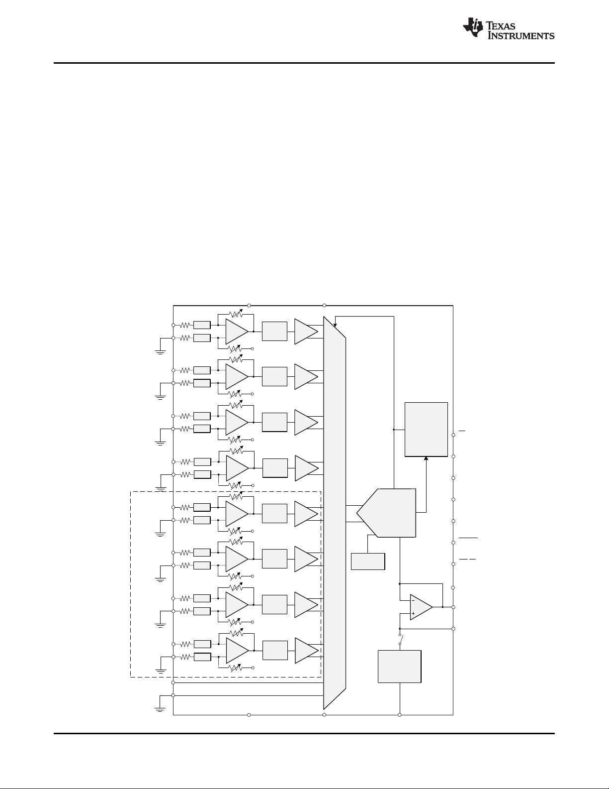
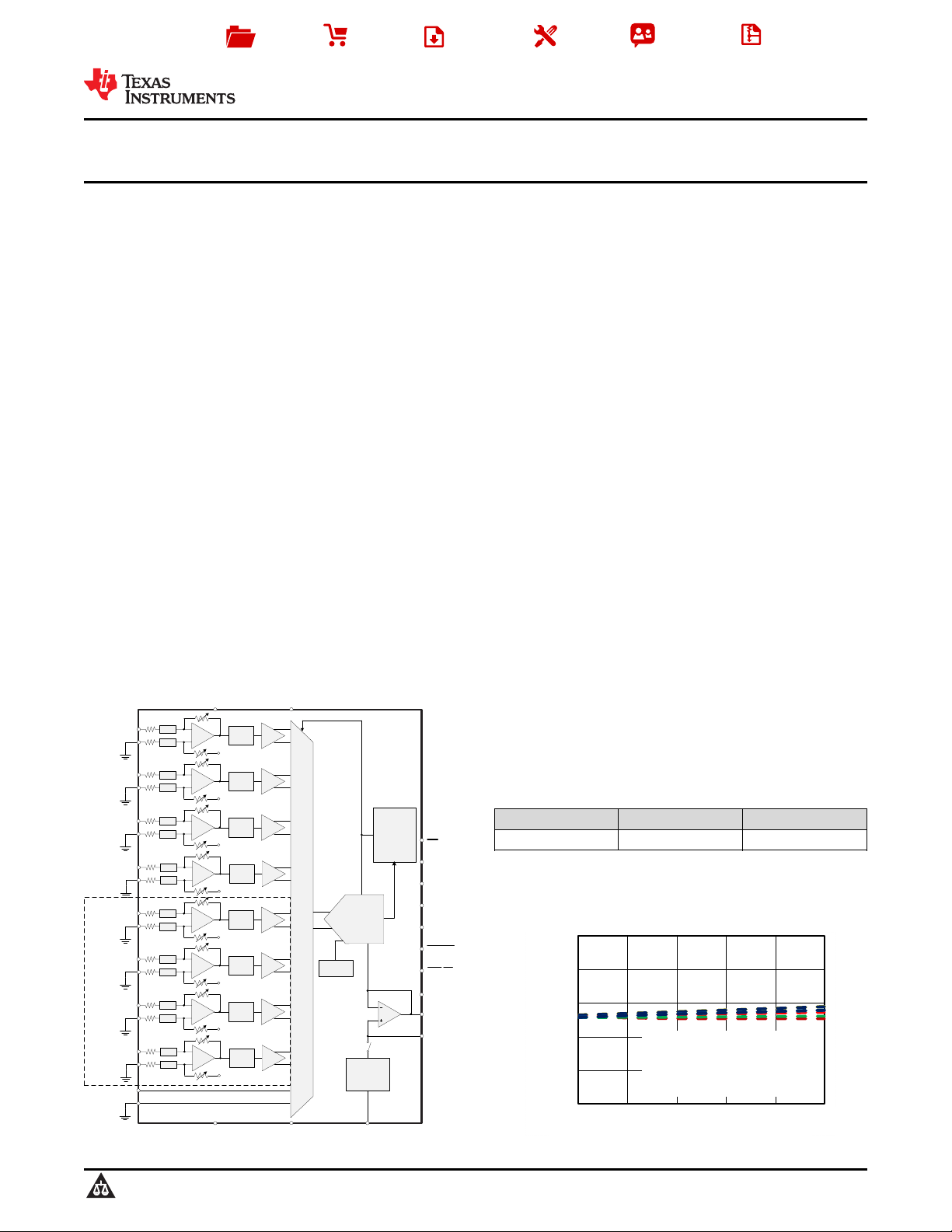
Multiplexer
Oscillator
PGA
1 M:
OVP
1 M:
2nd-Order
LPF
ADC
Driver
V
B0
AIN_0P
AIN_0GND
OVP
PGA
1 M:
OVP
1 M:
2nd-Order
LPF
ADC
Driver
V
B1
AIN_1P
AIN_1GND
OVP
PGA
1 M:
OVP
1 M:
2nd-Order
LPF
ADC
Driver
V
B2
AIN_2P
AIN_2GND
OVP
PGA
1 M:
OVP
1 M:
2nd-Order
LPF
ADC
Driver
V
B3
AIN_3P
AIN_3GND
OVP
PGA
1 M:
OVP
1 M:
2nd-Order
LPF
ADC
Driver
V
B4
AIN_4P
AIN_4GND
OVP
PGA
1 M:
OVP
1 M:
2nd-Order
LPF
ADC
Driver
V
B5
AIN_5P
AIN_5GND
OVP
PGA
1 M:
OVP
1 M:
2nd-Order
LPF
ADC
Driver
V
B6
AIN_6P
AIN_6GND
OVP
PGA
1 M:
OVP
1 M:
2nd-Order
LPF
ADC
Driver
V
B7
AIN_7P
AIN_7GND
OVP
AUX_IN
AUX_GND
12-Bit
SAR ADC
Digital
Logic
and
Interface
4.096-V
Reference
REFGND
DGNDAGND
DVDD
AVDD
Additional Channels in ADS8668
ADS8668
ADS8664
ALARM
CS
SCLK
SDI
SDO
DAISY
REFSEL
RST/PD
REFCAP
REFIO
ADS8664,ADS8668
SBAS492 –JULY 2015
www.ti.com
8 Detailed Description
8.1 Overview
The ADS8664 and ADS8668 are 12-bit data acquisition systems with 4- and 8-channel analog inputs,
respectively. Each analog input channel consists of an overvoltage protection circuit, a programmable gain
amplifier (PGA), and a second-order, antialiasing filter that conditions the input signal before being fed into a 4or 8-channel analog multiplexer (MUX). The output of the MUX is digitized using a 12-bit analog-to-digital
converter (ADC), based on the successive approximation register (SAR) architecture. This overall system can
achieve a maximum throughput of 500 kSPS, combined across all channels. The devices feature a 4.096-V
internal reference with a fast-settling buffer and a simple SPI-compatible serial interface with daisy-chain (DAISY)
and ALARM features.
The devices operate from a single 5-V analog supply and can accommodate true bipolar input signals up to
±2.5 × V
or the selected input range. The integration of multichannel precision analog front-end circuits with high input
impedance and a precision ADC operating from a single 5-V supply offers a simplified end solution without
requiring external high-voltage bipolar supplies and complicated driver circuits.
8.2 Functional Block Diagram
. The devices offer a constant 1-MΩ resistive input impedance irrespective of the sampling frequency
REF
22 Submit Documentation Feedback Copyright © 2015, Texas Instruments Incorporated
Product Folder Links: ADS8664 ADS8668
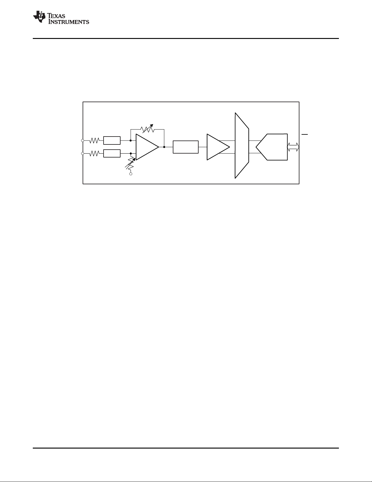
MUX
PGA
1 M:
OVP
1 M:
OVP
2nd-Order
LPF
ADC
Driver
V
B
ADC
AIN_nP
AIN_nGND
CS
SCLK
SDI
SDO
DAISY
ADS8664,ADS8668
www.ti.com
SBAS492 –JULY 2015
8.3 Feature Description
8.3.1 Analog Inputs
The ADS8664 and ADS8668 have either four or eight analog input channels, respectively, such that the positive
inputs AIN_nP (n = 0 to 3 or 7) are the single-ended analog inputs and the negative inputs AIN_nGND are tied to
GND. Figure 67 shows the simplified circuit schematic for each analog input channel, including the input
overvoltage protection circuit, PGA, low-pass filter (LPF), high-speed ADC driver, and analog multiplexer.
NOTE: n = 0 to 3 for the ADS8664 and n = 0 to 7 for the ADS8668.
Figure 67. Front-End Circuit Schematic for Each Analog Input Channel
The devices can support multiple unipolar or bipolar, single-ended input voltage ranges based on the
configuration of the program registers. As explained in the Range Select Registers section, the input voltage
range for each analog channel can be configured to bipolar ±2.5 × V
V
, and ±0.15625 × V
REF
V
. With the internal or external reference voltage set to 4.096 V, the input ranges of the device can be
REF
or unipolar 0 to 2.5 × V
REF
, 0 to 1.25 × V
REF
, ±1.25 × V
REF
, 0 to 0.625 × V
REF
, ±0.625 × V
REF
, ±0.3125 ×
REF
, and 0 to 0.3125 ×
REF
configured to bipolar ranges of ±10.24 V, ±5.12 V, ±2.56 V, ±1.28 V, and ±0.64 V or unipolar ranges of 0 V to
10.24 V, 0 V to 5.12 V, 0 V to 2.56 V, and 0 V to 1.28 V. Any of these input ranges can be assigned to any
analog input channel of the device. For instance, the ±2.5 × V
V
range can be assigned to AIN_2P, the 0 V to 2.5 × V
REF
REF
range can be assigned to AIN_1P, the ±1.25 ×
REF
range can be assigned to AIN_3P, and so forth.
The devices sample the voltage difference (AIN_nP – AIN_nGND) between the selected analog input channel
and the AIN_nGND pin. The devices allow a ±0.1-V range on the AIN_nGND pin for all analog input channels.
This feature is useful in modular systems where the sensor or signal-conditioning block is further away from the
ADC on the board and when a difference in the ground potential of the sensor or signal conditioner from the ADC
ground is possible. In such cases, running separate wires from the AIN_nGND pin of the device to the sensor or
signal-conditioning ground is recommended.
If the analog input pins (AIN_nP) to the devices are left floating, the output of the ADC corresponds to an internal
biasing voltage. The output from the ADC must be considered as invalid if the devices are operated with floating
input pins. This condition does not cause any damage to the devices, which are fully functional when a valid
input voltage is applied to the pins.
8.3.2 Analog Input Impedance
Each analog input channel in the device presents a constant resistive impedance of 1 MΩ. The input impedance
is independent of either the ADC sampling frequency, the input signal frequency, or range. The primary
advantage of such high-impedance inputs is the ease of driving the ADC inputs without requiring driving
amplifiers with low output impedance. Bipolar, high-voltage power supplies are not required in the system
because this ADC does not require any high-voltage front-end drivers. In most applications, the signal sources or
sensor outputs can be directly connected to the ADC input, thus significantly simplifying the design of the signal
chain.
In order to maintain the dc accuracy of the system, matching the external source impedance on the AIN_nP input
pin with an equivalent resistance on the AIN_nGND pin is recommended. This matching helps to cancel any
additional offset error contributed by the external resistance.
Copyright © 2015, Texas Instruments Incorporated Submit Documentation Feedback 23
Product Folder Links: ADS8664 ADS8668
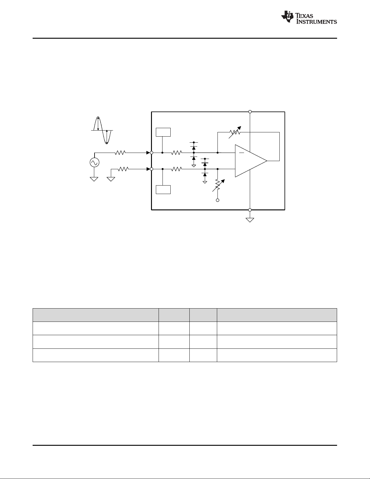
V
OUT
V
+
V
±
+
V
B
AVDD
GND
AIN_nP
AIN_nGND
10
10
R
DC
R
FB
0V
V
P+
V
P-
R
S
ESD
D1p
D2n
R
S
AVDD
AVDD
D2p
D1n
ESD
ADS8664,ADS8668
SBAS492 –JULY 2015
www.ti.com
Feature Description (continued)
8.3.3 Input Overvoltage Protection Circuit
The ADS8664 and ADS8668 feature an internal overvoltage protection circuit on each of the four or eight analog
input channels, respectively. Use these protection circuits as a secondary protection scheme to protect the
device. Using external protection devices against surges, electrostatic discharge (ESD), and electrical fast
transient (EFT) conditions is highly recommended. The conceptual block diagram of the internal overvoltage
protection (OVP) circuit is shown in Figure 68.
Figure 68. Input Overvoltage Protection Circuit Schematic
As shown in Figure 68, the combination of the 1-MΩ input resistors along with the PGA gain-setting resistors
(RFBand RDC) limit the current flowing into the input pins. A combination of antiparallel diodes (D1 and D2) are
added on each input pin to protect the internal circuitry and set the overvoltage protection limits.
Table 1 explains the various operating conditions for the device when the device is powered on. Table 1
indicates that when the AVDD pin of the device is connected to the proper supply voltage (AVDD = 5 V) or offers
a low impedance of < 30 kΩ, the internal overvoltage protection circuit can withstand up to ±20 V on the analog
input pins.
Table 1. Input Overvoltage Protection Limits When AVDD = 5 V or Offers a Low Impedance of < 30 kΩ
INPUT CONDITION TEST ADC
(V
= ±20 V) CONDITION OUTPUT
OVP
|VIN| < |V
|V
RANGE
|VIN| > |V
(1) GND = 0, AIN_nGND = 0 V, |V
for the internal OVP circuit. Assume that RSis approximately 0.
The results indicated in Table 1 are based on an assumption that the analog input pins are driven by very low
impedance sources (RSis approximately 0). However, if the sources driving the inputs have higher impedance,
the current flowing through the protection diodes reduces further, thereby increasing the OVP voltage range.
Note that higher source impedance results in gain errors and contributes to overall system noise performance.
| Within operating range Valid Device functions as per data sheet specifications
RANGE
| < |VIN| < |V
| Beyond overvoltage range Saturated
OVP
Beyond operating range but All input ADC output is saturated, but device is internally
| Saturated
OVP
within overvoltage range ranges protected (not recommended for extended time)
| is the maximum input voltage for any selected input range, and |V
RANGE
All input
ranges
All input This usage condition may cause irreversible damage
ranges to the device
COMMENTS
| is the break-down voltage
OVP
(1)
24 Submit Documentation Feedback Copyright © 2015, Texas Instruments Incorporated
Product Folder Links: ADS8664 ADS8668

±20
±12
±4
4
12
20
±20 ±12 ±4
4 12 20
Analog Input Current (µA)
Input Voltage (V)
C004
±30
±18
±6
6
18
30
±30 ±20 ± 10
0 10 20 30
Analog Input Current (uA)
Input Voltage (V)
C003
---- ± 2.5*V
REF,
---- 1.25*V
REF
---- 0.625*V
REF,
------0.3125*V
REF
-------0.156 V
REF,
---- + 2.5*V
REF
---- + 1.25*V
REF,
---- + 0.625*V
REF
---- + 0.3125*V
REF
ADS8664,ADS8668
www.ti.com
SBAS492 –JULY 2015
Figure 69 shows the voltage versus current response of the internal overvoltage protection circuit when the
device is powered on. According to this current-to-voltage (I-V) response, the current flowing into the device input
pins is limited by the 1-MΩ input impedance. However, for voltages beyond ±20 V, the internal node voltages
surpass the break-down voltage for internal transistors, thus setting the limit for overvoltage protection on the
input pins.
The same overvoltage protection circuit also provides protection to the device when the device is not powered on
and AVDD is floating with an impedance > 30 kΩ. This condition can arise when the input signals are applied
before the ADC is fully powered on. The overvoltage protection limits for this condition are shown in Table 2.
OVP
(1)
| is the
Table 2. Input Overvoltage Protection Limits When AVDD = Floating with Impedance > 30 kΩ
INPUT CONDITION TEST
(V
= ±11 V) CONDITION
OVP
|VIN| < |V
|VIN| > |V
(1) AVDD = floating, GND = 0, AIN_nGND = 0 V, |V
| Within overvoltage range All input ranges Invalid
OVP
| Beyond overvoltage range All input ranges Invalid
OVP
| is the maximum input voltage for any selected input range, and |V
break-down voltage for the internal OVP circuit. Assume that RSis approximately 0.
RANGE
ADC OUTPUT COMMENTS
Device is not functional but is protected internally by
the OVP circuit.
This usage condition may cause irreversible damage
to the device.
Figure 70 shows the voltage versus current response of the internal overvoltage protection circuit when the
device is not powered on. According to this I-V response, the current flowing into the device input pins is limited
by the 1-MΩ input impedance. However, for voltages beyond ±11 V, the internal node voltages surpass the
break-down voltage for internal transistors, thus setting the limit for overvoltage protection on the input pins.
Copyright © 2015, Texas Instruments Incorporated Submit Documentation Feedback 25
Figure 69. I-V Curve for an Input OVP Circuit
Figure 70. I-V Curve for an Input OVP Circuit
(AVDD = Floating)
Product Folder Links: ADS8664 ADS8668

±6
±5
±4
±3
±2
±1
0
50 500 5000 50000
Magnitude (dB)
Input Frequency (Hz)
C064
---- ± 2.5*V
REF,
---- 1.25*V
REF
---- 0.625*V
REF,
------0.3125*V
REF
-------0.156 V
REF,
---- + 2.5*V
REF
---- + 1.25*V
REF,
---- + 0.625*V
REF
---- + 0.3125*V
REF
±90
±75
±60
±45
±30
±15
0
100 1000 10000 100000
Phase (Degree)
Input Frequency (Hz)
C065
---- ± 2.5*V
REF,
---- 1.25*V
REF
---- 0.625*V
REF,
------0.3125*V
REF
-------0.156 V
REF,
---- + 2.5*V
REF
---- + 1.25*V
REF,
---- + 0.625*V
REF
---- + 0.3125*V
REF
ADS8664,ADS8668
SBAS492 –JULY 2015
www.ti.com
8.3.4 Programmable Gain Amplifier (PGA)
The devices offer a programmable gain amplifier (PGA) at each individual analog input channel, which converts
the original single-ended input signal into a fully-differential signal to drive the internal 12-bit ADC. The PGA also
adjusts the common-mode level of the input signal before being fed into the ADC to ensure maximum usage of
the ADC input dynamic range. Depending on the range of the input signal, the PGA gain can be accordingly
adjusted by setting the Range_CHn[3:0] (n = 0 to 3 or 7) bits in the program register. The default or power-on
state for the Range_CHn[3:0] bits is 0000, which corresponds to an input signal range of ±2.5 × V
. Table 3
REF
lists the various configurations of the Range_CHn[3:0] bits for the different analog input voltage ranges.
The PGA uses a very highly-matched network of resistors for multiple gain configurations. Matching between
these resistors and the amplifiers across all channels is accurately trimmed to keep the overall gain error low
across all channels and input ranges.
Table 3. Input Range Selection Bits Configuration
ANALOG INPUT RANGE
±2.5 × V
±1.25 × V
±0.625 × V
±0.3125 × V
±0.15625 × V
0 to 2.5 × V
0 to 1.25 × V
0 to 0.625 × V
0 to 0.3125 × V
REF
REF
REF
REF
REF
REF
REF
REF
REF
BIT 3 BIT 2 BIT 1 BIT 0
0 0 0 0
0 0 0 1
0 0 1 0
0 0 1 1
1 0 1 1
0 1 0 1
0 1 1 0
0 1 1 1
1 1 1 1
Range_CHn[3:0]
8.3.5 Second-Order, Low-Pass Filter (LPF)
In order to mitigate the noise of the front-end amplifiers and gain resistors of the PGA, each analog input channel
of the ADS8664 and ADS8668 features a second-order, antialiasing LPF at the output of the PGA. The
magnitude and phase response of the analog antialiasing filter are shown in Figure 71 and Figure 72,
respectively. For maximum performance, the –3-dB cutoff frequency for the antialiasing filter is typically set to
15 kHz. The performance of the filter is consistent across all input ranges supported by the ADC.
Figure 71. Second-Order LPF Magnitude Response Figure 72. Second-Order LPF Phase Response
26 Submit Documentation Feedback Copyright © 2015, Texas Instruments Incorporated
Product Folder Links: ADS8664 ADS8668

ADS8664,ADS8668
www.ti.com
SBAS492 –JULY 2015
8.3.6 ADC Driver
In order to meet the performance of a 12-bit, SAR ADC at the maximum sampling rate (500 kSPS), the sampleand-hold capacitors at the input of the ADC must be successfully charged and discharged during the acquisition
time window. This drive requirement at the inputs of the ADC necessitates the use of a high-bandwidth, lownoise, and stable amplifier buffer. Such an input driver is integrated in the front-end signal path of each analog
input channel of the device. During transition from one channel of the multiplexer to another channel, the fast
integrated driver ensures that the multiplexer output settles to a 12-bit accuracy within the acquisition time of the
ADC, irrespective of the input levels on the respective channels.
8.3.7 Multiplexer (MUX)
The ADS8664 and ADS8668 feature an integrated 4- and 8-channel analog multiplexer, respectively. For each
analog input channel, the voltage difference between the positive analog input AIN_nP and the negative ground
input AIN_nGND is conditioned by the analog front-end circuitry before being fed into the multiplexer. The output
of the multiplexer is directly sampled by the ADC. The multiplexer in the device can scan these analog inputs in
either manual or auto-scan mode, as explained in the Channel Sequencing Modes section. In manual mode
(MAN_Ch_n), the channel is selected for every sample via a register write; in auto-scan mode (AUTO_RST), the
channel number is incremented automatically on every CS falling edge after the present channel is sampled. The
analog inputs can be selected for an auto scan with register settings (see the Auto-Scan Sequencing Control
Registers section). The devices automatically scan only the selected analog inputs in ascending order.
The maximum overall throughput for the ADS8664 and ADS8668 is specified at 500 kSPS across all channels.
The per channel throughput is dependent on the number of channels selected in the multiplexer scanning
sequence. For example, the throughput per channel is equal to 250 kSPS if only two channels are selected, but
is equal to 125 kSPS per channel if four channels are selected (as in the ADS8664), and so forth.
See Table 6 for command register settings to switch between the auto-scan mode and manual mode for
individual analog channels.
8.3.8 Reference
The ADS8664 and ADS8668 can operate with either an internal voltage reference or an external voltage
reference using the internal buffer. The internal or external reference selection is determined by an external
REFSEL pin. The devices have a built-in buffer amplifier to drive the actual reference input of the internal ADC
core for maximizing performance.
Copyright © 2015, Texas Instruments Incorporated Submit Documentation Feedback 27
Product Folder Links: ADS8664 ADS8668

0
100
200
300
400
500
600
-1 -0.6 -0.2 0.2 0.6 1
Number of Devices
Error in REFIO Voltage (mV)
C064
ADC
4.096 V
REF
REFCAP
REFIO
AGND
22 PF
REFGND
10 PF
REFSEL
AVDD
1 PF
ADS8664,ADS8668
SBAS492 –JULY 2015
www.ti.com
8.3.8.1 Internal Reference
The devices have an internal 4.096-V (nominal value) reference. In order to select the internal reference, the
REFSEL pin must be tied low or connected to AGND. When the internal reference is used, REFIO (pin 5)
becomes an output pin with the internal reference value. Placing a 10-µF (minimum) decoupling capacitor
between the REFIO pin and REFGND (pin 6) is recommended, as shown in Figure 73. The capacitor must be
placed as close to the REFIO pin as possible. The output impedance of the internal band-gap circuit creates a
low-pass filter with this capacitor to band-limit the noise of the reference. The use of a smaller capacitor value
allows higher reference noise in the system, thus degrading SNR and SINAD performance. Do not use the
REFIO pin to drive external ac or dc loads because REFIO has limited current output capability. The REFIO pin
can be used as a source if followed by a suitable op amp buffer (such as the OPA320).
Figure 73. Device Connections for Using an Internal 4.096-V Reference
The device internal reference is trimmed to a maximum initial accuracy of ±1 mV. The histogram in Figure 74
shows the distribution of the internal voltage reference output taken from more than 3300 production devices.
28 Submit Documentation Feedback Copyright © 2015, Texas Instruments Incorporated
Figure 74. Internal Reference Accuracy at Room Temperature Histogram
Product Folder Links: ADS8664 ADS8668

4.09
4.091
4.092
4.093
4.094
4.095
4.096
4.097
4.098
4.099
4.1
±40 ±7
26 59 92 125
REFIO Voltage (V)
Free-Air Temperature (oC)
C053
----- AVDD = 5.25 V
------ AVDD = 5 V
------ AVDD = 4.75 V
0
4
8
12
16
20
1 2 3 4 5 6 7 8 9 10
Number of Devices
REFIO Drift (ppm/ºC)
C054
0
5
10
15
20
25
30
-4 -3 -2 -1 0 1
Number of Devices
Error in REFIO Voltage (mV)
C065
ADS8664,ADS8668
www.ti.com
SBAS492 –JULY 2015
The initial accuracy specification for the internal reference can be degraded if the die is exposed to any
mechanical or thermal stress. Heating the device when being soldered to a PCB and any subsequent solder
reflow is a primary cause for shifts in the V
value. The main cause of thermal hysteresis is a change in die
REF
stress and therefore is a function of the package, die-attach material, and molding compound, as well as the
layout of the device itself.
In order to illustrate this effect, 80 devices were soldered using lead-free solder paste with the manufacturer's
suggested reflow profile, as explained in application report SNOA550. The internal voltage reference output is
measured before and after the reflow process and the typical shift in value is shown in Figure 75. Although all
tested units exhibit a positive shift in their output voltages, negative shifts are also possible. Note that the
histogram in Figure 75 shows the typical shift for exposure to a single reflow profile. Exposure to multiple reflows,
which is common on PCBs with surface-mount components on both sides, causes additional shifts in the output
voltage. If the PCB is to be exposed to multiple reflows, solder the ADS8664 and ADS8668 in the second pass to
minimize device exposure to thermal stress.
Figure 75. Solder Heat Shift Distribution Histogram
The internal reference is also temperature compensated to provide excellent temperature drift over an extended
industrial temperature range of –40°C to 125°C. Figure 76 shows the variation of the internal reference voltage
across temperature for different values of the AVDD supply voltage. The typical specified value of the reference
voltage drift over temperature is 8 ppm/°C (Figure 77) and the maximum specified temperature drift is equal to
20 ppm/°C.
Figure 76. Variation of the Internal Reference Output Figure 77. Internal Reference Temperature Drift Histogram
(REFIO) Across Supply and Temperature
Copyright © 2015, Texas Instruments Incorporated Submit Documentation Feedback 29
Product Folder Links: ADS8664 ADS8668
AVDD = 5 V, number of devices = 30, ΔT = –40°C to 125°C

ADC
4.096 V
REF
REFCAP
REFIO
AGND
22 PF
REFGND
C
REF
REFSEL
AVDD
REF5040
(See the device datasheet for
a detailed pin configuration.)
AVDD
OUT
DVDD
1 PF
ADS8664,ADS8668
SBAS492 –JULY 2015
www.ti.com
8.3.8.2 External Reference
For applications that require a better reference voltage or a common reference voltage for multiple devices, the
ADS8664 and ADS8668 offer a provision to use an external reference along with an internal buffer to drive the
ADC reference pin. In order to select the external reference mode, either tie the REFSEL pin high or connect this
pin to the DVDD supply. In this mode, an external 4.096-V reference must be applied at REFIO (pin 5), which
becomes an input pin. Any low-power, low-drift, or small-size external reference can be used in this mode
because the internal buffer is optimally designed to handle the dynamic loading on the REFCAP pin, which is
internally connected to the ADC reference input. The output of the external reference must be appropriately
filtered to minimize the resulting effect of the reference noise on system performance. A typical connection
diagram for this mode is shown in Figure 78.
Figure 78. Device Connections for Using an External 4.096-V Reference
The output of the internal reference buffer appears at the REFCAP pin. A minimum capacitance of 10 µF must
be placed between REFCAP (pin 7) and REFGND (pin 6). Place another capacitor of 1 µF as close to the
REFCAP pin as possible for decoupling high-frequency signals. Do not use the internal buffer to drive external ac
or dc loads because of the limited current output capability of this buffer.
30 Submit Documentation Feedback Copyright © 2015, Texas Instruments Incorporated
Product Folder Links: ADS8664 ADS8668

4.095
4.0952
4.0954
4.0956
4.0958
4.096
4.0962
4.0964
4.0966
4.0968
4.097
±40 ±7
26 59 92 125
REFCAP Voltage (V)
Free-Air Temperature (oC)
C055
----- AVDD = 5.25 V
------ AVDD = 5 V
------ AVDD = 4.75 V
0
3
6
9
12
15
0 0.2 0.4 0.6 0.8 1 1.2
Number of Devices
REFCAP Drift (ppm/ºC)
C056
ADS8664,ADS8668
www.ti.com
SBAS492 –JULY 2015
The performance of the internal buffer output is very stable across the entire operating temperature range of
–40°C to 125°C. Figure 79 shows the variation in the REFCAP output across temperature for different values of
the AVDD supply voltage. The typical specified value of the reference buffer drift over temperature is 1 ppm/°C
(Figure 80) and the maximum specified temperature drift is equal to 1.5 ppm/°C.
AVDD = 5 V, number of devices = 30, ΔT = –40°C to 125°C
Figure 79. Variation of the Reference Buffer Output Figure 80. Reference Buffer Temperature Drift Histogram
(REFCAP) vs Supply and Temperature
8.3.9 Auxiliary Channel
The devices include a single-ended auxiliary input channel (AUX_IN and AUX_GND). The AUX channel provides
direct interface to an internal, high-precision, 12-bit ADC through the multiplexer because this channel does not
include the front-end analog signal conditioning that the other analog input channels have. The AUX channel
supports a single unipolar input range of 0 V to V
AUX_IN pin can vary from 0 V to V
, whereas the AUX_GND pin must be tied to GND.
REF
because there is no front-end PGA. The input signal on the
REF
When a conversion is initiated, the voltage between these pins is sampled directly on an internal sampling
capacitor (75 pF, typical). The input current required to charge the sampling capacitor is determined by several
factors, including the sampling rate, input frequency, and source impedance. For slow applications that use a
low-impedance source, the inputs of the AUX channel can be directly driven. When the throughput, input
frequency, or the source impedance increases, a driving amplifier must be used at the input to achieve good ac
performance from the AUX channel. Some key requirements of the driving amplifier are discussed in the Input
Driver for the AUX Channel section.
Copyright © 2015, Texas Instruments Incorporated Submit Documentation Feedback 31
Product Folder Links: ADS8664 ADS8668

±200
±160
±120
±80
±40
0
0 50000 100000 150000 200000 250000
Amplitude (dB)
Input Frequency (Hz)
C068
-90.35
-90.3
-90.25
-90.2
-90.15
-90.1
-90.05
-90
-89.95
-89.9
-89.85
70
72
74
76
-40 -7 26 59 92 125
SNR, SINAD (dB)
Free-Air Temperature (oC)
C069
SNR
THD
SINAD
THD (dB)
0
1000
2000
3000
4000
5000
2044 2045 2046 2047 2048 2049 2050 2051 2052
Number of Hits
Output Codes
C066
±4.0
±3.0
±2.0
±1.0
0.0
1.0
2.0
3.0
4.0
-0.3
-0.25
-0.2
-0.15
-0.1
-0.05
0
0.05
0.1
-40 -7 26 59 92 125
Offset Error (mV)
Gain Error (%FSR)
Free-Air Temperature (oC)
C067
Gain Error
Offset Error
ADS8664,ADS8668
SBAS492 –JULY 2015
www.ti.com
The AUX channel in the ADS8664 and ADS8668 offers a true 12-bit performance with no missing codes. Some
typical performance characteristics of the AUX channel are shown in Figure 81 to Figure 84.
Mean = 2048, sigma = 0
Figure 81. DC Histogram for Mid-Scale Input
(AUX Channel)
fIN= 1 kHz, SNR = 74.06 dB, SINAD = 74.03 dB,
THD = –95.40 dB, SFDR = 97.04 dB, number of points = 64k
Figure 83. Typical FFT Plot
(AUX Channel)
AUX channel
Figure 82. Offset and Gain vs Temperature
(AUX Channel)
fIN= 1 kHz
Figure 84. SNR, SINAD, and THD vs Temperature
(AUX Channel)
32 Submit Documentation Feedback Copyright © 2015, Texas Instruments Incorporated
Product Folder Links: ADS8664 ADS8668

_ _
_
.
2
SNR dB
1
AMP PP
2
FSR
f
20
G n RMS 3dB
V
V
1
6 6 2 5
2 2
S
§ ·
¨ ¸
u u u d u u
¨ ¸
© ¹
AMP ADC
3dB
t u
ADS8664,ADS8668
www.ti.com
SBAS492 –JULY 2015
8.3.9.1 Input Driver for the AUX Channel
For applications that use the AUX input channels at high throughput and high input frequency, a driving amplifier
with low output impedance is required to meet the ac performance of the internal 12-bit ADC. Some key
specifications of the input driving amplifier are discussed below:
• Small-signal bandwidth. The small-signal bandwidth of the input driving amplifier must be much higher than
the bandwidth of the AUX input to ensure that there is no attenuation of the input signal resulting from the
bandwidth limitation of the amplifier. In a typical data acquisition system, a low cut-off frequency, antialiasing
filter is used at the inputs of a high-resolution ADC. The amplifier driving the antialiasing filter must have a low
closed-loop output impedance for stability, thus implying a higher gain bandwidth for the amplifier. Higher
small-signal bandwidth also minimizes the harmonic distortion at higher input frequencies. In general, the
amplifier bandwidth requirements can be calculated on the basis of Equation 1.
where:
• f
is the 3-dB bandwidth of the RC filter. (1)
–3dB
• Distortion. In order to achieve the distortion performance of the AUX channel, the distortion of the input driver
must be at least 10 dB lower than the specified distortion of the internal ADC, as shown in Equation 2.
(2)
• Noise. Careful considerations must be made to select a low-noise, front-end amplifier in order to prevent any
degradation in SNR performance of the system. As a rule of thumb, to ensure that the noise performance of
the data acquisition system is not limited by the front-end circuit, keep the total noise contribution from the
front-end circuit below 20% of the input-referred noise of the ADC. Noise from the input driver circuit is bandlimited by the low cut-off frequency of the input antialiasing filter, as explained in Equation 3.
where:
• V
1 / f_AMP_PP
• e
n_RMS
• NGis the noise gain of the front-end circuit, which is equal to 1 in a buffer configuration. (3)
is the peak-to-peak flicker noise,
is the amplifier broadband noise density in nV/√Hz, and
Copyright © 2015, Texas Instruments Incorporated Submit Documentation Feedback 33
Product Folder Links: ADS8664 ADS8668

001h
FFFh
800h
FSR ± 1LSB
FSR/21LSB
ADC Output Code
Analog Input (AIN_nP t AIN_nGND)
NFS
PFS
ADS8664,ADS8668
SBAS492 –JULY 2015
www.ti.com
8.3.10 ADC Transfer Function
The ADS8664 and ADS8668 are a family of multichannel devices that support single-ended, bipolar, and
unipolar input ranges on all input channels. The output of the devices is in straight binary format for both bipolar
and unipolar input ranges. The format for the output codes is the same across all analog channels.
The ideal transfer characteristic for each ADC channel for all input ranges is shown in Figure 85. The full-scale
range (FSR) for each input signal is equal to the difference between the positive full-scale (PFS) input voltage
and the negative full-scale (NFS) input voltage. The LSB size is equal to FSR / 212= FSR / 4096 because the
resolution of the ADC is 12 bits. For a reference voltage of V
= 4.096 V, the LSB values corresponding to the
REF
different input ranges are listed in Table 4.
Figure 85. 12-Bit ADC Transfer Function (Straight-Binary Format)
Table 4. ADC LSB Values for Different Input Ranges (V
INPUT RANGE POSITIVE FULL-SCALE NEGATIVE FULL-SCALE FULL-SCALE RANGE LSB (mV)
±2.5 × V
±1.25 × V
±0.625 × V
REF
REF
REF
±0.3125 × V
±0.15625 × V
0 to 2.5 × V
0 to 1.25 × V
0 to 0.625 × V
0 to 0.3125 × V
REF
REF
REF
REF
REF
REF
10.24 V –10.24 V 20.48 V 5.00
5.12 V –5.12 V 10.24 V 2.50
2.56 V –2.56 V 5.12 V 1.25
1.28 V –1.28 V 2.56 V 0.625
0.64 V –0.64 V 1.28 V 0.3125
10.24 V 0 V 10.24 V 2.50
5.12 V 0 V 5.12 V 1.25
2.56 V 0 V 2.56 V 0.625
1.28 V 0 V 1.28 V 0.3125
= 4.096 V)
REF
34 Submit Documentation Feedback Copyright © 2015, Texas Instruments Incorporated
Product Folder Links: ADS8664 ADS8668

ADC Output
Channel n
Alarm Threshold
Channel n
+/-
Hysteresis Channel n
+
S Q
QR
Alarm Flag Read
Active Alarm Flag
Channel n
Tripped Alarm Flag
Channel n
All Channel
H/L Alarms
SDO
ALARM
ADC
16
th
SCLK
Alarm Threshold
ADC Output
H_ALARM On
H_ALARM Off
(T ± H ± 2)
(T + H)
ADC Output
L_ALARM Off
L_ALARM On
(T + H + 1)(T ± H ± 1)
Alarm Threshold
ADS8664,ADS8668
www.ti.com
SBAS492 –JULY 2015
8.3.11 Alarm Feature
The devices have an active-high ALARM output on pin 35. The ALARM signal is synchronous and changes its
state on the 16th falling edge of the SCLK signal. A high level on ALARM indicates that the alarm flag has
tripped on one or more channels of the device. This pin can be wired to interrupt the host input. When an
ALARM interrupt is received, the alarm flag registers are read to determine which channels have an alarm. The
devices feature independently-programmable alarms for each channel. There are two alarms per channel (a low
and a high alarm) and each alarm threshold has a separate hysteresis setting.
The ADS8664 and ADS8668 set a high alarm when the digital output for a particular channel exceeds the high
alarm upper limit [high alarm threshold (T) + hysteresis (H)]. The alarm resets when the digital output for the
channel is less than or equal to the high alarm lower limit (high alarm T – H – 2). This function is shown in
Figure 86.
Similarly, the lower alarm is triggered when the digital output for a particular channel falls below the low alarm
lower limit (low alarm threshold T – H – 1). The alarm resets when the digital output for the channel is greater
than or equal to the low alarm higher limit (low alarm T + H + 1). This function is shown in Figure 87.
Figure 86. High-ALARM Hysteresis
Figure 87. Low-ALARM Hysteresis
Figure 88 shows a functional block diagram for a single-channel alarm. There are two flags for each high and low
alarm: active alarm flag and tripped alarm flag; see the Alarm Flag Registers (Read-Only) section for more
details. The active alarm flag is triggered when an alarm condition is encountered for a particular channel; the
active alarm flag resets when the alarm shuts off. A tripped alarm flag sets an alarm condition in the same
manner as for an active alarm flag. However, the tripped alarm flag remains latched and resets only when the
appropriate alarm flag register is read.
Copyright © 2015, Texas Instruments Incorporated Submit Documentation Feedback 35
Figure 88. Alarm Functionality Schematic
Product Folder Links: ADS8664 ADS8668

CS
SCLK
SDI
SDO
DAISY
ADS8664
ADS8668
SDON (from previous device)
or DGND
CS
SCLK
SDO
SDI
Host Controller
RST / PD
RST / PD
ADS8664,ADS8668
SBAS492 –JULY 2015
8.4 Device Functional Modes
8.4.1 Device Interface
8.4.1.1 Digital Pin Description
The digital data interface for the ADS8664 and ADS8668 is shown in Figure 89.
Figure 89. Pin Configuration for the Digital Interface
www.ti.com
The signals shown in Figure 89 are summarized as follows:
8.4.1.1.1 CS (Input)
CS indicates an active-low, chip-select signal. CS is also used as a control signal to trigger a conversion on the
falling edge. Each data frame begins with the falling edge of the CS signal. The analog input channel to be
converted during a particular frame is selected in the previous frame. On the CS falling edge, the devices sample
the input signal from the selected channel and a conversion is initiated using the internal clock. The device
settings for the next data frame can be input during this conversion process. When the CS signal is high, the
ADC is considered to be in an idle state.
8.4.1.1.2 SCLK (Input)
This pin indicates the external clock input for the data interface. All synchronous accesses to the device are
timed with respect to the falling edges of the SCLK signal.
8.4.1.1.3 SDI (Input)
SDI is the serial data input line. SDI is used by the host processor to program the internal device registers for
device configuration. At the beginning of each data frame, the CS signal goes low and the data on the SDI line
are read by the device at every falling edge of the SCLK signal for the next 16 SCLK cycles. Any changes made
to the device configuration in a particular data frame are applied to the device on the subsequent falling edge of
the CS signal.
8.4.1.1.4 SDO (Output)
SDO is the serial data output line. SDO is used by the device to output conversion data. The size of the data
output frame varies depending on the register setting for the SDO format; see Table 13. A low level on CS
releases the SDO pin from the Hi-Z state. SDO is kept low for the first 15 SCLK falling edges. The MSB of the
output data stream is clocked out on SDO on the 16th SCLK falling edge, followed by the subsequent data bits
on every falling edge thereafter. The SDO line goes low after the entire data frame is output and goes to a Hi-Z
state when CS goes high.
36 Submit Documentation Feedback Copyright © 2015, Texas Instruments Incorporated
Product Folder Links: ADS8664 ADS8668

RST / PD
t
PL_RST_PD
ADS8664,ADS8668
www.ti.com
SBAS492 –JULY 2015
Device Functional Modes (continued)
8.4.1.1.5 DAISY (Input)
DAISY is a serial input pin. When multiple devices are connected in daisy-chain mode, as illustrated in Figure 92,
the DAISY pin of the first device in the chain is connected to GND. The DAISY pin of every subsequent device is
connected to the SDO output pin of the previous device, and the SDO output of the last device in the chain goes
to the SDI of the host processor. If an application uses a stand-alone device, the DAISY pin is connected to
GND.
8.4.1.1.6 RST/PD (Input)
RST/PD is a dual-function pin. Figure 90 shows the timing of this pin and Table 5 explains the usage of this pin.
Figure 90. RST/PD Pin Timing
Table 5. RST/PD Pin Functionality
CONDITION DEVICE MODE
40 ns < t
100 ns < t
t
PL_RST_PD
PL_RST_PD
PL_RST_PD
≤ 100 ns The device is in RST mode and does not enter PWR_DN mode.
< 400 ns
≥ 400 ns
The device is in RST mode and may or may not enter PWR_DN mode.
NOTE: This setting is not recommended.
The device enters PWR_DN mode and the program registers are reset to default
value.
The devices can be placed into power-down (PWR_DN) mode by pulling the RST/PD pin to a logic low state for
at least 400 ns. The RST/PD pin is asynchronous to the clock; thus, RST/PD can be triggered at any time
regardless of the status of other pins (including the analog input channels). When the device is in power-down
mode, any activity on the digital input pins (apart from the RST/PD pin) is ignored.
The program registers in the device can be reset to their default values (RST) by pulling the RST/PD pin to a
logic low state for no longer than 100 ns. This input is asynchronous to the clock. When RST/PD is pulled back
to a logic high state, the devices are placed in normal mode. One valid write operation must be executed on the
program register in order to configure the device, followed by an appropriate command (AUTO_RST or MAN) to
initiate conversions.
When the RST/PD pin is pulled back to a logic high level, the devices wake-up in a default state in which the
program registers are reset to their default values.
Copyright © 2015, Texas Instruments Incorporated Submit Documentation Feedback 37
Product Folder Links: ADS8664 ADS8668

1 2 14 15 16 17
23 24
25
26
27 28 29
30SCLK
CS
D5 D4 D3
D2 D1
D0
SDO
Sample
N
Sample
N + 1
Data from sample N
31 32
D11
D10
18
B15
B14 B2
B1 B0
X X X X X X X X X
SDI
7 8 9
B9 B8 B7
B10
B3
1 2 3 4
ADS8664,ADS8668
SBAS492 –JULY 2015
www.ti.com
8.4.1.2 Data Acquisition Example
This section provides an example of how a host processor can use the device interface to configure the device
internal registers as well as convert and acquire data for sampling a particular input channel. The timing diagram
shown in Figure 91 provides further details.
Figure 91. Device Operation Using the Serial Interface Timing Diagram
There are four events shown in Figure 91. These events are described below:
• Event 1: The host initiates a data conversion frame through a falling edge of the CS signal. The analog input
signal at the instant of the CS falling edge is sampled by the ADC and conversion is performed using an
internal oscillator clock. The analog input channel converted during this frame is selected in the previous data
frame. The internal register settings of the device for the next conversion can be input during this data frame
using the SDI and SCLK inputs. Initiate SCLK at this instant and latch data on the SDI line into the device on
every SCLK falling edge for the next 16 SCLK cycles. At this instant, SDO goes low because the device does
not output internal conversion data on the SDO line during the first 16 SCLK cycles.
• Event 2: During the first 16 SCLK cycles, the device completes the internal conversion process and data are
now ready within the converter. However, the device does not output data bits on SDO until the 16th falling
edge appears on the SCLK input. Because the ADC conversion time is fixed (the maximum value is given in
the Electrical Characteristics table), the 16th SCLK falling edge must appear after the internal conversion is
over, otherwise data output from the device is incorrect. Therefore, the SCLK frequency cannot exceed a
maximum value, as provided in the Timing Requirements: Serial Interface table.
• Event 3: At the 16th falling edge of the SCLK signal, the device reads the LSB of the input word on the SDI
line. The device does not read anything from the SDI line for the remaining data frame. On the same edge,
the MSB of the conversion data is output on the SDO line and can be read by the host processor on the
subsequent falling edge of the SCLK signal. For 12 bits of output data, the LSB can be read on the 28th
SCLK falling edge. The SDO outputs 0 on subsequent SCLK falling edges until the next conversion is
initiated.
• Event 4: When the internal data from the device is received, the host terminates the data frame by
deactivating the CS signal to high. The SDO output goes into a Hi-Z state until the next data frame is initiated,
as explained in Event 1.
8.4.1.3 Host-to-Device Connection Topologies
The digital interface of the ADS8664 and ADS8668 offers a lot of flexibility in the ways that a host controller can
exchange data or commands with the device. A typical connection between a host controller and a stand-alone
device is illustrated in Figure 89. However, there are applications that require multiple ADCs but the host
controller has limited interfacing capability. This section describes two connection topologies that can be used to
address the requirements of such applications.
38 Submit Documentation Feedback Copyright © 2015, Texas Instruments Incorporated
Product Folder Links: ADS8664 ADS8668

1 2 15 16 17
SCLK
CS
Sample
N
Sample
N + 1
t
S
29 32
18
B15
B14
X
X X X
SDI
X
B1 B0 XB2
33 34
43 44
45 48
X
X
X X X
X
SDO
3
Data from Sample N
ADC
3
SDO2,
3
SDO1,
2
{D11}
1
{D10}
1
{D1}
1
{D0}
1
{D11}
2
{D10}
2
{D1}
2
{D0}
2
{D11}
3
{D10}
3
{D1}
3
{D0}
3
{D11}
1
{D10}
1
{D1}
1
{D0}
1
{D11}
2
{D10}
2
{D1}
2
{D0}
2
{D11}
1
{D10}1{D1}
1
{D0}
1
Data from Sample N
ADC
2
Data from Sample N
ADC
1
27 28 50
59 60
61 6449
X
X
X
X XX
CS SDISCLK
DAISY
1
SDO
1
SDI
ADC
1
ADC
2
ADC
N
CS
SDO
SCLK
Host Controller
CS SDISCLK
DAISY
2
SDO
2
CS
SDISCLK
DAISY
N
SDO
N
ADS8664,ADS8668
www.ti.com
8.4.1.3.1 Daisy-Chain Topology
SBAS492 –JULY 2015
A typical connection diagram showing multiple devices in daisy-chain mode is shown in Figure 92. The CS,
SCLK, and SDI inputs of all devices are connected together and controlled by a single CS, SCLK, and SDO pin
of the host controller, respectively. The DAISY1input pin of the first ADC in the chain is connected to DGND, the
SDO1output pin is connected to the DAISY2input of ADC2, and so forth. The SDONpin of the Nth ADC in the
chain is connected to the SDI pin of the host controller. The devices do not require any special hardware or
software configuration to enter daisy-chain mode.
Figure 92. Daisy-Chain Connection Schematic
A typical timing diagram for three devices connected in daisy-chain mode is shown in Figure 93.
At the falling edge of the CS signal, all devices sample the input signal at their respective selected channels and
enter into conversion phase. For the first 16 SCLK cycles, the internal register settings for the next conversion
can be entered using the SDI line that is common to all devices in the chain. During this time period, the SDO
outputs for all devices remain low. At the end of conversion, every ADC in the chain loads its own conversion
result into an internal 16-bit shift register. For the 12-bit device, the internal shift register is loaded with 12 bits of
output data followed by 0000 in the LSB. At the 16th SCLK falling edge, every ADC in the chain outputs the MSB
bit on its own SDO output pin. On every subsequent SCLK falling edge, the internal shift register of each ADC
latches the data available on its DAISY pin and shifts out the next bit of data on its SDO pin. Therefore, the
digital host receives the data of ADCN, followed by the data of ADC
total, a minimum of 16 × N SCLK falling edges are required to capture the outputs of all N devices in the chain.
This example uses three devices in a daisy-chain connection, so 3 × 16 = 48 SCLK cycles are required to
capture the outputs of all devices in the chain along with the 16 SCLK cycles to input the register settings for the
next conversion, resulting in a total of 64 SCLK cycles for the entire data frame. Note that the overall throughput
of the system is proportionally reduced with the number of devices connected in a daisy-chain configuration.
Copyright © 2015, Texas Instruments Incorporated Submit Documentation Feedback 39
Figure 93. Three Devices Connected in Daisy-Chain Mode Timing Diagram
, and so forth (in MSB-first fashion). In
N–1
Product Folder Links: ADS8664 ADS8668

CS
SDO
SCLK
SDI
CS
SDO
SCLK
SDI
CS
SDO
SCLK
SDI
SDO
SCLK
ADC
1
ADC
2
ADC
N
SDI
CS
1
CS
2
CS
N
Host Controller
ADS8664,ADS8668
SBAS492 –JULY 2015
www.ti.com
The following points must be noted about the daisy-chain configuration illustrated in Figure 92:
• The SDI pins for all devices are connected together so each device operates with the same internal
configuration. This limitation can be overcome by spending additional host controller resources to control the
CS or SDI input of devices with unique configurations.
• If the number of devices connected in daisy-chain is more than four, loading increases on the shared output
lines from the host controller (CS, SDO, and SCLK). This increased loading can lead to digital timing errors.
This limitation can be overcome by using digital buffers on the shared outputs from the host controller before
feeding the shared digital lines into additional devices.
8.4.1.3.2 Star Topology
A typical connection diagram showing multiple devices in the star topology is shown in Figure 94. The SDI and
SCLK inputs of all devices are connected together and are controlled by a single SDO and SCLK pin of the host
controller, respectively. Similarly, the SDO outputs of all devices are tied together and connected to the SDI input
pin of the host controller. The CS input pin of each device is individually controlled by separate CS control lines
from the host controller.
Figure 94. Star Topology Connection Schematic
The timing diagram for a typical data frame in the star topology is the same as in a stand-alone device operation,
as illustrated in Figure 91. The data frame for a particular device starts with the falling edge of the CS signal and
ends when the CS signal goes high. Because the host controller provides separate CS control signals for each
device in this topology, the user can select the devices in any order and initiate a conversion by bringing down
the CS signal for that particular device. As explained in Figure 91, when CS goes high at the end of each data
frame, the SDO output of the device is placed into a Hi-Z state. Therefore, the shared SDO line in the star
topology is controlled only by the device with an active data frame (CS is low). In order to avoid any conflict
related to multiple devices driving the SDO line at the same time, ensure that the host controller pulls down the
CS signal for only one device at any particular time.
TI recommends connecting a maximum of four devices in the star topology. Beyond that, loading may increase
on the shared output lines from the host controller (SDO and SCLK). This loading can lead to digital timing
errors. This limitation can be overcome by using digital buffers on the shared outputs from the host controller
before being fed into additional devices.
40 Submit Documentation Feedback Copyright © 2015, Texas Instruments Incorporated
Product Folder Links: ADS8664 ADS8668

STANDBY
(STDBY)
POWER
DOWN
(PWR_DN)
PROGRAM
REGISTER
(PROG)
STDBY
PWR
_
DN
STDBY
PROG
PWR_DN
PROG
NO
_
OP
NO
_
OP
NO_OP
MANUAL
Channel n
(MAN_Ch_n)
AUTO
Ch. Scan
(AUTO)
AUTO Seq.
RESET
(AUTO_RST)
MAN_
Ch
_
n
MAN
_
Ch
_
n
AUTO
NO_OP
AUTO_RST
AUTO
_
RST
NO
_
OP
NO_OP
MAN_Ch_n
IDLE
Device waits for a
valid command to
initiate conversion
RESET
(RST)
Program Registers
are set to default
values
STDBY
/
PWR
_
DN
/
PROG
MAN_
Ch_
n
/
AUTO
_
RST
NO_OPRST
MAN_Ch_n / AUTO_RST
STDBY / PWR_DN / PROG
STDBY / PWR_DN / PROG
RST
MAN
_
Ch_n / AUTO
_
RST
RST
IDLE
ADS8664,ADS8668
www.ti.com
SBAS492 –JULY 2015
8.4.2 Device Modes
The ADS8664 and ADS8668 support multiple modes of operation that are software programmable. After
powering up, the device is placed into idle mode and does not perform any function until a command is received
from the user. Table 6 lists all commands to enter the different modes of the device. After power-up, the program
registers wake up with the default values and require appropriate configuration settings before performing any
conversion. The diagram in Figure 95 explains how to switch the device from one mode of operation to another.
Figure 95. State Transition Diagram
8.4.2.1 Continued Operation in the Selected Mode (NO_OP)
Holding the SDI line low continuously (equivalent to writing a 0 to all 16 bits) during device operation continues
device operation in the last selected mode (STDBY, PWR_DN, AUTO_RST, or MAN_Ch_n). In this mode, the
device follows the same settings that are already configured in the program registers.
If a NO_OP condition occurs when the device is performing any read or write operation in the program register
(PROG mode), then the device retains the current settings of the program registers. The device goes back to
IDLE mode and waits for the user to enter a proper command to execute the program register read or write
configuration.
Copyright © 2015, Texas Instruments Incorporated Submit Documentation Feedback 41
Product Folder Links: ADS8664 ADS8668

1 2 14 15
16 17
18 28 29 32
CS
D1
SDO
Data from Sample N
D11
D10
D0
STDBY Command ± 8200h
SDI
X
X X X X X
X X
Sample N
Enters STDBY on
CS Rising Edge
CS can go high immediately after Standby
command or after reading frame data.
1 2 14 15
16
Stays in STDBY
if SDI is Low in a
Data Frame
ADS8664,ADS8668
SBAS492 –JULY 2015
www.ti.com
8.4.2.2 Frame Abort Condition (FRAME_ABORT)
As explained in the Data Acquisition Example section, the device digital interface is designed such that each data
frame starts with a falling edge of the CS signal. During the first 16 SCLK cycles, the device reads the 16-bit
command word on the SDI line. The device waits to execute the command until the last bit of the command is
received, which is latched on the 16th SCLK falling edge. During this operation, the CS signal must stay low. If
the CS signal goes high for any reason before the data transmission is complete, the device goes into an
INVALID state and waits for a proper command to be written. This condition is called the FRAME_ABORT
condition. When the device is operating in this INVALID mode, any read operation on the device returns invalid
data on the SDO line. The output of the ALARM pin will continue to reflect the status of input signal on the
previously selected channel.
8.4.2.3 STANDBY Mode (STDBY)
The devices support a low-power standby mode (STDBY) in which only part of the circuit is powered down. The
internal reference and buffer is not powered down, and therefore, the devices can be quickly powered up in 20
µs on exiting the STDBY mode. When the device comes out of STDBY mode, the program registers are not
reset to the default values.
To enter STDBY mode, execute a valid write operation to the command register with a STDBY command of
8200h, as shown in Figure 96. The command is executed and the device enters STDBY mode on the next CS
rising edge following this write operation. The device remains in STDBY mode if no valid conversion command
(AUTO_RST or MAN_Ch_n) is executed and SDI remains low (see the Continued Operation in the Selected
Mode section) during the subsequent data frames. When the device operates in STDBY mode, the program
register settings can be updated (as explained in the Program Register Read/Write Operation section) using 16
SCLK cycles. However, if 32 complete SCLK cycles are provided, then the device returns invalid data on the
SDO line because there is no ongoing conversion in STDBY mode. The program register read operation can
take place normally during this mode.
42 Submit Documentation Feedback Copyright © 2015, Texas Instruments Incorporated
Figure 96. Enter and Remain in STDBY Mode Timing Diagram
Product Folder Links: ADS8664 ADS8668

1 2 12 13 14 15
16
CS
SDO
AUTO_RST Command
MAN_CH_n Command
SDI
9 10 11
3 4 5
6 7 8
Device exits
STDBY Mode on
CS Rising Edge
Min width of CS HIGH = 20µs
for valid sample
ADS8664,ADS8668
www.ti.com
SBAS492 –JULY 2015
In order to exit STDBY mode a valid 16-bit write command must be executed to enter auto (AUTO_RST) or
manual (MAN_CH_n) scan mode, as shown in Figure 97. The device starts exiting STDBY mode on the next CS
rising edge. At the next CS falling edge, the device samples the analog input at the channel selected by the
MAN_CH_n command or the first channel of the AUTO_RST mode sequence. To ensure that the input signal is
sampled correctly, keep the minimum width of the CS signal at 20 µs after exiting STDBY mode so the device
internal circuitry can be fully powered up and biased properly before taking the sample. The data output for the
selected channel can be read during the same data frame, as explained in Figure 91.
Figure 97. Exit STDBY Mode Timing Diagram
Copyright © 2015, Texas Instruments Incorporated Submit Documentation Feedback 43
Product Folder Links: ADS8664 ADS8668

1 2 12 13 14 15
16
CS
SDO
AUTO_RST Command
MAN_CH_n Command
SDI
9 10 11
3 4 5
6 7 8
Device exits PWR_DN Mode, but
waits 15ms for 16-bit settling
First 16-bit accurate data
frame after recovery from
PWR_DN mode
Invalid Data
1 2 14 15
16 17
18 28 29 32
CS
D1
SDO
Data from Sample N
D11
D10
D0
PWR_DN Command ± 8300h
SDI
X
X X X X X
X X
Sample
N
Enters PWR_DN on
CS Rising Edge
CS can go high immediately after PWR_DN
command or after reading frame data.
1 2 14 15
16
Stays in PWR_DN
if SDI is Low in a
Data Frame
ADS8664,ADS8668
SBAS492 –JULY 2015
www.ti.com
8.4.2.4 Power-Down Mode (PWR_DN)
The devices support a hardware and software power-down mode (PWR_DN) in which all internal circuitry is
powered down, including the internal reference and buffer. A minimum time of 15 ms is required for the device to
power up and convert the selected analog input channel after exiting PWR_DN mode, if the device is operating
in the internal reference mode (REFSEL = 0). The hardware power mode for the device is explained in the
RST/PD (Input) section. The primary difference between the hardware and software power-down modes is that
the program registers are reset to default values when the devices wake up from hardware power-down, but the
previous settings of the program registers are retained when the devices wake up from software power-down.
To enter PWR_DN mode using software, execute a valid write operation on the command register with a
software PWR_DN command of 8300h, as shown in Figure 98. The command is executed and the device enters
PWR_DN mode on the next CS rising edge following this write operation. The device remains in PWR_DN mode
if no valid conversion command (AUTO_RST or MAN_Ch_n) is executed and SDI remains low (see the
Continued Operation in the Selected Mode section) during the subsequent data frames. When the device
operates in PWR_DN mode, the program register settings can be updated (as explained in the Program Register
Read/Write Operation section) using 16 SCLK cycles. However, if 32 complete SCLK cycles are provided, then
the device returns invalid data on the SDO line because there is no ongoing conversion in PWR_DN mode. The
program register read operation can take place normally during this mode.
Figure 98. Enter and Remain in PWR_DN Mode Timing Diagram
In order to exit from PWR_DN mode a valid 16-bit write command must be executed, as shown in Figure 99. The
device comes out of PWR_DN mode on the next CS rising edge. For operation in internal reference mode
(REFSEL = 0), 15 ms are required for the device to power-up the reference and other internal circuits and settle
to the required accuracy before valid conversion data are output for the selected input channel.
44 Submit Documentation Feedback Copyright © 2015, Texas Instruments Incorporated
Figure 99. Exit PWR_DN Mode Timing Diagram
Product Folder Links: ADS8664 ADS8668

AUTO_RST
Sample
N
SDI
SDO
CS
xxxx
Sample N Data
Ch 0
Sample
0000h xxxx
Ch 0 Data
Ch 1
Sample
0000h xxxx
Ch 1 Data
Ch 2
Sample
AUTO_RST xxxx
Ch 2 Data
Based on Previous
Mode Setting
Ch 0
Sample
0000h xxxx
Ch 0 Data
AUTO_RST Mode
(Channel sequence restarted from
lowest count.)
AUTO_RST Mode
(Channels 0-2 are selected in sequence.)
1 2 14 15
16 17
18 28 29 32
CS
D1
SDO
Data from Sample N
D11
D10
D0
AUTO_RST Command ± A000h
SDI
X
X X X X X
X X
Sample N
Enters AUTO_RST mode on CS Rising Edge
Samples 1st Ch. of Auto-Ch Sequence
CS can go high immediately after AUTO_RST
command or after reading frame data.
1 2 14 15
16
Stays in AUTO_RST Mode if
SDI is Low in a Data Frame
27
28
Samples 2nd Ch. of
Auto-Ch Sequence
Data from 1st Ch of Seq.
32
ADS8664,ADS8668
www.ti.com
SBAS492 –JULY 2015
8.4.2.5 Auto Channel Enable with Reset (AUTO_RST)
The devices can be programmed to scan the input signal on all analog channels automatically by writing a valid
auto channel sequence with a reset (AUTO_RST, A000h) command in the command register, as explained in
Figure 100. As shown in Figure 100, the CS signal can be pulled high immediately after the AUTO_RST
command or after reading the output data of the frame. However, in order to accurately acquire and convert the
input signal on the first selected channel in the next data frame, the command frame must be a complete frame
of 32 SCLK cycles.
The sequence of channels for the automatic scan can be configured by the AUTO SCAN sequencing control
register (01h to 02h) in the program register; see the Program Register Map section. In this mode, the devices
continuously cycle through the selected channels in ascending order, beginning with the lowest channel and
converting all channels selected in the program register. On completion of the sequence, the devices return to
the lowest count channel in the program register and repeat the sequence. The input voltage range for each
channel in the auto-scan sequence can be configured by setting the Range Select Registers of the program
registers.
The devices remain in AUTO_RST mode if no other valid command is executed and SDI is kept low (see the
Continued Operation in the Selected Mode (NO_OP) section) during subsequent data frames. If the AUTO_RST
command is executed again at any time during this mode of operation, then the sequence of the scanned
channels is reset. The devices return to the lowest count channel of the auto-scan sequence in the program
register and repeat the sequence. The timing diagram in Figure 101 shows this behavior using an example in
which channels 0 to 2 are selected in the auto sequence. For switching between AUTO_RST mode and
MAN_Ch_n mode; see the Channel Sequencing Modes section.
Copyright © 2015, Texas Instruments Incorporated Submit Documentation Feedback 45
Figure 100. Enter AUTO_RST Mode Timing Diagram
Figure 101. Device Operation Example in AUTO_RST Mode
Product Folder Links: ADS8664 ADS8668

MAN_Ch_1
Sample
N
SDI
SDO
CS
xxxx
Sample N Data
Ch 1
Sample
0000h xxxx
Ch 1 Data
Ch 1
Sample
0000h xxxx
Ch 1 Data
Ch 1
Sample
MAN_Ch_3 xxxx
Ch 1 Data
Based on Previous
Mode Setting
Ch 3
Sample
0000h xxxx
Ch 3 Data
MAN_Ch_n Mode
(Ch 1 is selected and device continuously converts Ch 1 if NO_OP command is provided)
MAN_Ch_n Mode
(Transition from Ch1 to Ch 3)
1 2 14 15
16 17
18 28 29 32
CS
D1
SDO
Data from Sample N
D11
D10
D0
MAN_Ch_n Command
SDI
X
X X X X X
X X
Sample N
Enters MAN_Ch_n Mode on CS Rising Edge
1st Sample of Manual Channel n
CS can go high immediately after MAN_Ch_n
command or after reading frame data.
1 2 14 15
16
Stays in MAN_Ch_n Mode if
SDI is Low in a Data Frame
27
28
2nd Sample of Manual Ch. n
Sample 1 of Channel n
32
ADS8664,ADS8668
SBAS492 –JULY 2015
www.ti.com
8.4.2.6 Manual Channel n Select (MAN_Ch_n)
The devices can be programmed to convert a particular analog input channel by operating in manual channel n
scan mode (MAN_Ch_n). This programming is done by writing a valid manual channel n select command
(MAN_Ch_n) in the command register, as shown in Figure 102. As shown in Figure 102, the CS signal can be
pulled high immediately after the MAN_Ch_n command or after reading the output data of the frame. However, in
order to accurately acquire and convert the input signal on the next channel, the command frame must be a
complete frame of 32 SCLK cycles. See Table 6 for a list of commands to select individual channels during
MAN_Ch_n mode.
Figure 102. Enter MAN_Ch_n Scan Mode Timing Diagram
The manual channel n select command (MAN_Ch_n) is executed and the devices sample the analog input on
the selected channel on the CS falling edge of the next data frame following this write operation. The input
voltage range for each channel in the MAN_Ch_n mode can be configured by setting the Range Select Registers
in the program registers. The device continues to sample the analog input on the same channel if no other valid
command is executed and SDI is kept low (see the Continued Operation in the Selected Mode (NO_OP) section)
during subsequent data frames. The timing diagram in Figure 103 shows this behavior using an example in
which channel 1 is selected in the manual sequencing mode. For switching between MAN_Ch_n mode and
AUTO_RST mode; see the Channel Sequencing Modes section.
Figure 103. Device Operation in MAN_Ch_n Mode
46 Submit Documentation Feedback Copyright © 2015, Texas Instruments Incorporated
Product Folder Links: ADS8664 ADS8668

MAN_Ch_2
SDI
SDO
AUTO_RST ModeMAN_Ch_n Mode
CS
xxxx
Ch 2
Sample
AUTO_RST xxxx
Ch 2 Data
Ch 0
Sample
0000h xxxx
Ch 0 Data
Ch 5
Sample
0000h xxxx
Ch 5 Data
Sample
N
Sample N Data
Based on Previous
Mode Setting
0000h
Ch 0
Sample
SDI
SDO
MAN_Ch_n ModeAUTO_RST Mode
CS
xxxx
Ch 0 Data
Ch 5
Sample
MAN_Ch_1 xxxx
Ch 5 Data
Ch 1
Sample
MAN_Ch_3 xxxx
Ch 1 Data
Ch 3
Sample
MAN_Ch_n xxxx
Ch 3 Data
ADS8664,ADS8668
www.ti.com
SBAS492 –JULY 2015
8.4.2.7 Channel Sequencing Modes
The devices offer two channel sequencing modes: AUTO_RST and MAN_Ch_n.
In AUTO_RST mode, the channel number automatically increments in every subsequent frame. As explained in
the Auto-Scan Sequencing Control Registers section, the analog inputs can be selected for an automatic scan
with a register setting. The device automatically scans only the selected analog inputs in ascending order. The
unselected analog input channels can also be powered down for optimizing power consumption in this mode of
operation. The auto-mode sequence can be reset at any time during an automatic scan (using the AUTO_RST
command). When the reset command is received, the ongoing auto-mode sequence is reset and restarts from
the lowest selected channel in the sequence.
In MAN_Ch_n mode, the same input channel is selected during every data conversion frame. The input
command words to select individual analog channels in MAN_Ch_n mode are listed in Table 6. If a particular
input channel is selected during a data frame, then the analog inputs on the same channel are sampled during
the next data frame. Figure 104 shows the SDI command sequence for transitions from AUTO_RST to
MAN_Ch_n mode.
Figure 104. Transitioning from AUTO_RST to MAN_Ch_n Mode
(Channels 0 and 5 are Selected for Auto Sequence)
Figure 105 shows the SDI command sequence for transitions from MAN_Ch_n to AUTO_RST mode. Note that
each SDI command is executed on the next CS falling edge. A RST command can be issued at any instant
during any channel sequencing mode, after which the device is placed into a default power-up state in the next
data frame.
Figure 105. Transitioning from MAN_Ch_n to AUTO_RST Mode
Copyright © 2015, Texas Instruments Incorporated Submit Documentation Feedback 47
(Channels 0 and 5 are Selected for Auto Sequence)
Product Folder Links: ADS8664 ADS8668

1 2 13 14 15
16 17
18 28 29 32
CS
D1
SDO
Data from Sample N
D11
D10
D0
Reset Program Registers (RST) ± 8500h
SDI
X
X X X X X
3 4 5
X X
Sample N
All Program
Registers are Reset
to Default Values on
CS Rising Edge
CS can go high immediately after RST
command or after reading frame data.
ADS8664,ADS8668
SBAS492 –JULY 2015
www.ti.com
8.4.2.8 Reset Program Registers (RST)
The devices support a hardware and software reset (RST) mode in which all program registers are reset to their
default values. The devices can be put into RST mode using a hardware pin, as explained in the RST/PD (Input)
section.
The device program registers can be reset to their default values during any data frame by executing a valid
write operation on the command register with a RST command of 8500h, as shown in Figure 106. The device
remains in RST mode if no valid conversion command (AUTO_RST or MAN_Ch_n) is executed and SDI remains
low (see the Continued Operation in the Selected Mode (NO_OP) section) during the subsequent data frames.
When the device operates in RST mode, the program register settings can be updated (as explained in the
Program Register Read/Write Operation section) using 16 SCLK cycles. However, if 32 complete SCLK cycles
are provided, then the device returns invalid data on the SDO line because there is no ongoing conversion in
RST mode. The values of the program register can be read normally during this mode. A valid AUTO_RST or
MAN_CH_n channel selection command must be executed for initiating a conversion on a particular analog
channel using the default program register settings.
Figure 106. Reset Program Registers (RST) Timing Diagram
48 Submit Documentation Feedback Copyright © 2015, Texas Instruments Incorporated
Product Folder Links: ADS8664 ADS8668

ADS8664,ADS8668
www.ti.com
SBAS492 –JULY 2015
8.5 Register Maps
The internal registers of the ADS8664 and ADS8668 are categorized into two categories: command registers and
program registers.
The command registers are used to select the channel sequencing mode (AUTO_RST or MAN_Ch_n), configure
the device in standby (STDBY) or power-down (PWR_DN) mode, and reset (RST) the program registers to their
default values.
The program registers are used to select the sequence of channels for AUTO_RST mode, select the SDO output
format, control input range settings for individual channels, control the ALARM feature, reading the alarm flags,
and programming the alarm thresholds for each channel.
8.5.1 Command Register Description
The command register is a 16-bit, write-only register that is used to set the operating modes of the ADS8664 and
ADS8668. The settings in this register are used to select the channel sequencing mode (AUTO_RST or
MAN_Ch_n), configure the device in standby (STDBY) or power-down (PWR_DN) mode, and reset (RST) the
program registers to their default values. All command settings for this register are listed in Table 6. During
power-up or reset, the default content of the command register is all 0's and the device waits for a command to
be written before being placed into any mode of operation. See Figure 1 for a typical timing diagram for writing a
16-bit command into the device. The device executes the command at the end of this particular data frame when
the CS signal goes high.
Table 6. Command Register Map
REGISTER OPERATION IN NEXT FRAME
Continued Operation
(NO_OP)
Standby
(STDBY)
Power Down
(PWR_DN)
Reset program registers
(RST)
Auto Ch. Sequence with Reset
(AUTO_RST)
Manual Ch 0 Selection
(MAN_Ch_0)
Manual Ch 1 Selection
(MAN_Ch_1)
Manual Ch 2 Selection
(MAN_Ch_2)
Manual Ch 3 Selection
(MAN_Ch_3)
Manual Ch 4 Selection
(MAN_Ch_4)
Manual Ch 5 Selection
(MAN_Ch_5)
Manual Ch 6 Selection
(MAN_Ch_6)
Manual Ch 7 Selection
(MAN_Ch_7)
Manual AUX Selection
(MAN_AUX)
(1)
B15 B14 B13 B12 B11 B10 B9 B8 B[7:0]
0 0 0 0 0 0 0 0 0000 0000 0000h Continue operation in previous mode
1 0 0 0 0 0 1 0 0000 0000 8200h Deviceis placed into standby mode
1 0 0 0 0 0 1 1 0000 0000 8300h Deviceis powered down
1 0 0 0 0 1 0 1 0000 0000 8500h Programregister is reset to default
1 0 1 0 0 0 0 0 0000 0000 A000h Auto mode enabled following a reset
1 1 0 0 0 0 0 0 0000 0000 C000h Channel 0 input is selected
1 1 0 0 0 1 0 0 0000 0000 C400h Channel 1 input is selected
1 1 0 0 1 0 0 0 0000 0000 C800h Channel 2 input is selected
1 1 0 0 1 1 0 0 0000 0000 CC00h Channel 3 input is selected
1 1 0 1 0 0 0 0 0000 0000 D000h Channel 4 input is selected
1 1 0 1 0 1 0 0 0000 0000 D400h Channel 5 input is selected
1 1 0 1 1 0 0 0 0000 0000 D800h Channel 6 input is selected
1 1 0 1 1 1 0 0 0000 0000 DC00h Channel 7 input is selected
1 1 1 0 0 0 0 0 0000 0000 E000h AUX channel input is selected
MSB BYTE LSB BYTE
(1) Shading indicates bits or registers not included in the 4-channel version of the device.
COMMAND
(Hex)
Copyright © 2015, Texas Instruments Incorporated Submit Documentation Feedback 49
Product Folder Links: ADS8664 ADS8668

1 2
15
16
CS
SDO
ADDR [6:0]
WR
DIN [7:0]
SDI
9 10
6 7 8
Data written into register, DIN [7:0]
23
24
17 18
X X X X
Sample
N
ADS8664,ADS8668
SBAS492 –JULY 2015
www.ti.com
8.5.2 Program Register Description
The program register is a 16-bit register used to set the operating modes of the ADS8664 and ADS8668. The
settings in this register are used to select the channel sequence for AUTO_RST mode, configure the device ID in
daisy-chain mode, select the SDO output format, control input range settings for individual channels, control the
ALARM feature, reading the alarm flags, and programming the alarm thresholds for each channel. All program
settings for this register are listed in Table 9. During power-up or reset, the different program registers in the
device wake up with their default values and the device waits for a command to be written before being placed
into any mode of operation.
8.5.2.1 Program Register Read/Write Operation
The program register is a 16-bit read or write register. There must be a minimum of 24 SCLKs after the CS
falling edge for any read or write operation to the program registers. When CS goes low, the SDO line goes low
as well. The device receives the command (see Table 7 and Table 8) through SDI where the first seven bits (bits
15-9) represent the register address and the eighth bit (bit 8) is the write or read instruction.
For a write cycle, the next eight bits (bits 7-0) on SDI are the desired data for the addressed register. Over the
next eight SCLK cycles, the device outputs this 8-bit data that is written into the register. This data readback
allows verification to determine if the correct data are entered into the device. A typical timing diagram for a
program register write cycle is shown in Figure 107.
Table 7. Write Cycle Command Word
PIN
SDI ADDR[6:0] 1 DIN[7:0]
REGISTER ADDRESS WR/RD DATA
(Bits 15-9) (Bit 8) (Bits 7-0)
Figure 107. Program Register Write Cycle Timing Diagram
50 Submit Documentation Feedback Copyright © 2015, Texas Instruments Incorporated
Product Folder Links: ADS8664 ADS8668

1 2
15
16
CS
SDO
ADDR [6:0]
RD
X X X X X X
SDI
9 10
6 7 8
DOUT [7:0]
23
24
17 18
ADS8664,ADS8668
www.ti.com
SBAS492 –JULY 2015
For a read cycle, the next eight bits (bits 7-0) on SDI are don’t care bits and SDO stays low. From the 16th SCLK
falling edge and onwards, SDO outputs the 8-bit data from the addressed register during the next eight clocks, in
MSB-first fashion. A typical timing diagram for a program register read cycle is shown in Figure 108.
Table 8. Read Cycle Command Word
PIN
SDI ADDR[6:0] 0 XXXXX
SDO 0000 000 0 DOUT[7:0]
REGISTER ADDRESS WR/RD DATA
(Bits 15-9) (Bit 8) (Bits 7-0)
Figure 108. Program Register Read Cycle Timing Diagram
Copyright © 2015, Texas Instruments Incorporated Submit Documentation Feedback 51
Product Folder Links: ADS8664 ADS8668

ADS8664,ADS8668
SBAS492 –JULY 2015
www.ti.com
8.5.2.2 Program Register Map
This section provides a bit-by-bit description of each program register.
Table 9. Program Register Map
REGISTER ADDRESS BIT 7 BIT 6 BIT 5 BIT 4 BIT 3 BIT 2 BIT 1 BIT 0
REGISTER
BITS[15:9]
AUTO SCAN SEQUENCING CONTROL
AUTO_SEQ_EN 01h FFh CH7_EN
Channel Power Down 02h 00h CH7_PD CH6_PD CH5_PD CH4_PD CH3_PD CH2_PD CH1_PD CH0_PD
DEVICE FEATURES SELECTION CONTROL
Feature Select 03h 00h DEV[1:0] 0 ALARM_EN0 0 SDO [2:0]
RANGE SELECT REGISTERS
Channel 0 Input Range 05h 00h 0 0 0 0 Range Select Channel 0[3:0]
Channel 1 Input Range 06h 00h 0 0 0 0 Range Select Channel 1[3:0]
Channel 2 Input Range 07h 00h 0 0 0 0 Range Select Channel 2[3:0]
Channel 3 Input Range 08h 00h 0 0 0 0 Range Select Channel 3[3:0]
Channel 4 Input Range 09h 00h 0 0 0 0 Range Select Channel 4[3:0]
Channel 5 Input Range 0Ah 00h 0 0 0 0 Range Select Channel 5[3:0]
Channel 6 Input Range 0Bh 00h 0 0 0 0 Range Select Channel 6[3:0]
Channel 7 Input Range 0Ch 00h 0 0 0 0 Range Select Channel 7[3:0]
ALARM FLAG REGISTERS (Read-Only)
ALARM Overview Tripped-Flag 10h 00h
ALARM Ch 0-3 Tripped-Flag 11h 00h
ALARM Ch 0-3 Active-Flag 12h 00h
ALARM Ch 4-7 Tripped-Flag 13h 00h
ALARM Ch 4-7 Active-Flag 14h 00h
(1) All registers are reset to the default values at power-on or at device reset using the register settings method.
(2) Shading indicates bits or registers that are not included in the 4-channel version of the device. A write operation on any of these bits or registers has no effect on device behavior. A read
operation on any of these bits or registers outputs all 1's on the SDO line.
DEFAULT
VALUE
(1)
(2)
Tripped Alarm Tripped Alarm Tripped Alarm Tripped Alarm Tripped Alarm Tripped Alarm Tripped Alarm Tripped Alarm
Flag Ch7 Flag Ch6 Flag Ch5 Flag Ch4 Flag Ch3 Flag Ch2 Flag Ch1 Flag Ch0
Tripped Alarm Tripped Alarm Tripped Alarm Tripped Alarm Tripped Alarm Tripped Alarm Tripped Alarm Tripped Alarm
Flag Ch0 Low Flag Ch0 High Flag Ch1 Low Flag Ch1 High Flag Ch2 Low Flag Ch2 High Flag Ch3 Low Flag Ch3 High
Active Alarm Active Alarm Active Alarm Active Alarm Active Alarm Active Alarm Active Alarm Active Alarm
Flag Ch0 Low Flag Ch0 High Flag Ch1 Low Flag Ch1 High Flag Ch2 Low Flag Ch2 High Flag Ch3 Low Flag Ch3 High
Tripped Alarm Tripped Alarm Tripped Alarm Tripped Alarm Tripped Alarm Tripped Alarm Tripped Alarm Tripped Alarm
Flag Ch4 Low Flag Ch4 High Flag Ch5 Low Flag Ch5 High Flag Ch6 Low Flag Ch6 High Flag Ch7 Low Flag Ch7 High
Active Alarm Active Alarm Active Alarm Active Alarm Active Alarm Active Alarm Active Alarm Active Alarm
Flag Ch4 Low Flag Ch4 High Flag Ch5 Low Flag Ch5 High Flag Ch6 Low Flag Ch6 High Flag Ch7 Low Flag Ch7 High
CH6_EN CH5_EN CH4_EN CH3_EN CH2_EN CH1_EN CH0_EN
52 Submit Documentation Feedback Copyright © 2015, Texas Instruments Incorporated
Product Folder Links: ADS8664 ADS8668

ADS8664,ADS8668
www.ti.com
Table 9. Program Register Map (continued)
REGISTER ADDRESS BIT 7 BIT 6 BIT 5 BIT 4 BIT 3 BIT 2 BIT 1 BIT 0
REGISTER
BITS[15:9]
ALARM THRESHOLD REGISTERS
Ch 0 Hysteresis 15h 00h CH0_HYST[3:0] 0 0 0 0
Ch 0 High Threshold MSB 16h FFh CH0_HT[11:4]
Ch 0 High Threshold LSB 17h F0h CH0_HT[3:0] 0 0 0 0
Ch 0 Low Threshold MSB 18h 00h CH0_LT[11:4]
Ch 0 Low Threshold LSB 19h 00h CH0_LT[3:0] 0 0 0 0
… … … See the Alarm Threshold Setting Registers for details regarding the ALARM threshold settings registers.
Ch 7 Hysteresis 38h 00h CH7_HYST[3:0] 0 0 0 0
Ch 7 High Threshold MSB 39h FFh CH7_HT[11:4]
Ch 7 High Threshold LSB 3Ah F0h CH7_HT[3:0] 0 0 0 0
Ch 7 Low Threshold MSB 3Bh 00h CH7_LT[11:4]
Ch 7 Low Threshold LSB 3Ch 00h CH7_LT[3:0] 0 0 0 0
COMMAND READ BACK (Read-Only)
Command Read Back 3Fh 00h COMMAND_WORD[7:0]
DEFAULT
VALUE
(1)
…
…
SBAS492 –JULY 2015
Copyright © 2015, Texas Instruments Incorporated Submit Documentation Feedback 53
Product Folder Links: ADS8664 ADS8668

ADS8664,ADS8668
SBAS492 –JULY 2015
www.ti.com
8.5.2.3 Program Register Descriptions
8.5.2.3.1 Auto-Scan Sequencing Control Registers
In AUTO_RST mode, the device automatically scans the preselected channels in ascending order with a new
channel selected for every conversion. Each individual channel can be selectively included in the auto channel
sequencing. For channels not selected for auto sequencing, the analog front-end circuitry can be individually
powered down.
8.5.2.3.1.1 Auto-Scan Sequence Enable Register (address = 01h)
This register selects individual channels for sequencing in AUTO_RST mode. The default value for this register is
FFh, which implies that in default condition all channels are included in the auto-scan sequence. If no channels
are included in the auto sequence (that is, the value for this register is 00h), then channel 0 is selected for
conversion by default.
Figure 109. AUTO_SEQ_EN Register
7 6 5 4 3 2 1 0
CH7_EN
LEGEND: R/W = Read/Write; -n = value after reset
(1) Shading indicates bits or registers that are not included in the 4-channel version of the device. A write operation on any of these bits or
(1)
R/W-1h R/W-1h R/W-1h R/W-1h R/W-1h R/W-1h R/W-1h R/W-1h
registers has no effect on device behavior. A read operation on any of these bits or registers outputs all 1's on the SDO line.
CH6_EN CH5_EN CH4_EN CH3_EN CH2_EN CH1_EN CH0_EN
Table 10. AUTO_SEQ_EN Field Descriptions
Bit Field Type Reset Description
7 CH7_EN R/W 1h Channel 7 enable.
6 CH6_EN R/W 1h Channel 6 enable.
5 CH5_EN R/W 1h Channel 5 enable.
4 CH4_EN R/W 1h Channel 4 enable.
3 CH3_EN R/W 1h Channel 3 enable.
2 CH2_EN R/W 1h Channel 2 enable.
1 CH1_EN R/W 1h Channel 1 enable.
0 CH0_EN R/W 1h Channel 0 enable.
0 = Channel 7 is not selected for sequencing in AUTO_RST mode
1 = Channel 7 is selected for sequencing in AUTO_RST mode
0 = Channel 6 is not selected for sequencing in AUTO_RST mode
1 = Channel 6 is selected for sequencing in AUTO_RST mode
0 = Channel 5 is not selected for sequencing in AUTO_RST mode
1 = Channel 5 is selected for sequencing in AUTO_RST mode
0 = Channel 4 is not selected for sequencing in AUTO_RST mode
1 = Channel 4 is selected for sequencing in AUTO_RST mode
0 = Channel 3 is not selected for sequencing in AUTO_RST mode
1 = Channel 3 is selected for sequencing in AUTO_RST mode
0 = Channel 2 is not selected for sequencing in AUTO_RST mode
1 = Channel 2 is selected for sequencing in AUTO_RST mode
0 = Channel 1 is not selected for sequencing in AUTO_RST mode
1 = Channel 1 is selected for sequencing in AUTO_RST mode
0 = Channel 0 is not selected for sequencing in AUTO_RST mode
1 = Channel 0 is selected for sequencing in AUTO_RST mode
54 Submit Documentation Feedback Copyright © 2015, Texas Instruments Incorporated
Product Folder Links: ADS8664 ADS8668

ADS8664,ADS8668
www.ti.com
8.5.2.3.1.2 Channel Power Down Register (address = 02h)
SBAS492 –JULY 2015
This register powers down individual channels that are not included for sequencing in AUTO_RST mode. The
default value for this register is 00h, which implies that in default condition all channels are powered up. If all
channels are powered down (that is, the value for this register is FFh), then the analog front-end circuits for all
channels are powered down and the output of the ADC contains invalid data. If the device is in MAN-Ch_n mode
and the selected channel is powered down, then the device yields invalid output that can also trigger a false
alarm condition.
Figure 110. Channel Power Down Register
7 6 5 4 3 2 1 0
CH7_PD
LEGEND: R/W = Read/Write; -n = value after reset
(1) Shading indicates bits or registers that are not included in the 4-channel version of the device. A write operation on any of these bits or
(1)
R/W-0h R/W-0h R/W-0h R/W-0h R/W-0h R/W-0h R/W-0h R/W-0h
registers has no effect on device behavior. A read operation on any of these bits or registers outputs all 1's on the SDO line.
CH6_PD CH5_PD CH4_PD CH3_PD CH2_PD CH1_PD CH0_PD
Table 11. Channel Power Down Register Field Descriptions
Bit Field Type Reset Description
7 CH7_PD R/W 0h Channel 7 power-down.
6 CH6_PD R/W 0h Channel 6 power-down.
5 CH5_PD R/W 0h Channel 5 power-down.
4 CH4_PD R/W 0h Channel 4 power-down.
3 CH3_PD R/W 0h Channel 3 power-down.
2 CH2_PD R/W 0h Channel 2 power-down.
1 CH1_PD R/W 0h Channel 1 power-down.
0 CH0_PD R/W 0h Channel 0 power-down.
0 = The analog front-end on channel 7 is powered up and channel 7 can be
included in the AUTO_RST sequence
1 = The analog front-end on channel 7 is powered down and channel 7
cannot be included in the AUTO_RST sequence
0 = The analog front-end on channel 6 is powered up and channel 6 can be
included in the AUTO_RST sequence
1 = The analog front-end on channel 6 is powered down and channel 6
cannot be included in the AUTO_RST sequence
0 = The analog front-end on channel 5 is powered up and channel 5 can be
included in the AUTO_RST sequence
1 = The analog front-end on channel 5 is powered down and channel 5
cannot be included in the AUTO_RST sequence
0 = The analog front-end on channel 4 is powered up and channel 4 can be
included in the AUTO_RST sequence
1 = The analog front-end on channel 4 is powered down and channel 4
cannot be included in the AUTO_RST sequence
0 = The analog front-end on channel 3 is powered up and channel 3 can be
included in the AUTO_RST sequence
1 = The analog front end on channel 3 is powered down and channel 3
cannot be included in the AUTO_RST sequence
0 = The analog front end on channel 2 is powered up and channel 2 can be
included in the AUTO_RST sequence
1 = The analog front end on channel 2 is powered down and channel 2
cannot be included in the AUTO_RST sequence
0 = The analog front end on channel 1 is powered up and channel 1 can be
included in the AUTO_RST sequence
1 = The analog front end on channel 1 is powered down and channel 1
cannot be included in the AUTO_RST sequence
0 = The analog front end on channel 0 is powered up and channel 0 can be
included in the AUTO_RST sequence
1 = The analog front end on channel 0 is powered down and channel 0
cannot be included in the AUTO_RST sequence
Copyright © 2015, Texas Instruments Incorporated Submit Documentation Feedback 55
Product Folder Links: ADS8664 ADS8668

ADS8664,ADS8668
SBAS492 –JULY 2015
8.5.2.3.2 Device Features Selection Control Register (address = 03h)
www.ti.com
The bits in this register can be used to configure the device ID for daisy-chain operation, enable the ALARM
feature, and configure the output bit format on SDO.
Figure 111. Feature Select Register
7 6 5 4 3 2 1 0
DEV[1:0] 0 ALARM_EN 0 SDO[2:0]
R/W-0h R-0h R/W-0h R-0h R/W-0h
LEGEND: R/W = Read/Write; R = Read only; -n = value after reset
Table 12. Feature Select Register Field Descriptions
Bit Field Type Reset Description
7-6 DEV[1:0] R/W 0h Device ID bits.
5 0 R 0h Must always be set to 0
4 0 R/W 0h ALARM feature enable.
3 0 R 0h Must always be set to 0
2-0 SDO[2:0] R/W 0h SDO data format bits (see Table 13).
00 = ID for device 0 in daisy-chain mode
01 = ID for device 1 in daisy-chain mode
10 = ID for device 2 in daisy-chain mode
11 = ID for device 3 in daisy-chain mode
0 = ALARM feature is disabled
1 = ALARM feature is enabled
Table 13. Description of Program Register Bits for SDO Data Format
SDO FORMAT BEGINNING OF THE
SDO[2:0] OUTPUT BIT STREAM
000 SDO pulled low
001 SDO pulled low
010
011
(1) Table 14 lists the bit descriptions for these channel addresses, device addresses, and input range.
16th SCLK falling edge, Conversion result for selected
no latency channel (MSB-first)
16th SCLK falling edge, Conversion result for selected Channel
no latency channel (MSB-first) address
16th SCLK falling edge, Conversion result for selected Channel Device SDO pulled
no latency channel (MSB-first) address
16th SCLK falling edge, Conversion result for selected Channel Device Input
no latency channel (MSB-first) address
BITS 24-9 BITS 8-5 BITS 4-3 BITS 2-0
OUTPUT FORMAT
(1)
(1)
(1)
address
address
(1)
(1)
low
range
(1)
Table 14. Bit Description for the SDO Data
BIT BIT DESCRIPTION
24-9 12 bits of conversion result for the channel represented in MSB-first format followed by 0000.
Four bits of channel address.
0000 = Channel 0
0001 = Channel 1
8-5 0011 = Channel 3
4-3 Two bits of device address (mainly useful in daisy-chain mode).
2-0 Three LSB bits of input voltage range (see the Range Select Registers section).
0010 = Channel 2
0100 = Channel 4 (valid only for the ADS8668)
0101 = Channel 5 (valid only for the ADS8668)
0110 = Channel 6 (valid only for the ADS8668)
0111 = Channel 7 (valid only for the ADS8668)
56 Submit Documentation Feedback Copyright © 2015, Texas Instruments Incorporated
Product Folder Links: ADS8664 ADS8668

ADS8664,ADS8668
www.ti.com
8.5.2.3.3 Range Select Registers (addresses 05h-0Ch)
SBAS492 –JULY 2015
Address 05h corresponds to channel 0, address 06h corresponds to channel 1, address 07h corresponds to
channel 2, address 08h corresponds to channel 3, address 09h corresponds to channel 4, address 0Ah
corresponds to channel 5, address 0Bh corresponds to channel 6, and address 0Ch corresponds to channel 7.
These registers allow the selection of input ranges for all individual channels (n = 0 to 3 for the ADS8664 and n =
0 to 7 for the ADS8668). The default value for these registers is 00h.
Figure 112. Channel n Input Range Registers
7 6 5 4 3 2 1 0
0 0 0 0 Range_CHn[3:0]
R-0h R-0h R-0h R-0h R/W-0h
LEGEND: R/W = Read/Write; R = Read only; -n = value after reset
Table 15. Channel n Input Range Registers Field Descriptions
Bit Field Type Reset Description
7-4 0 R 0h Must always be set to 0
3-0 Range_CHn[3:0] R/W 0h Input range selection bits for channel n (n = 0 to 3 for the ADS8664 and
n = 0 to 7 for the ADS8668).
0000 = Input range is set to ±2.5 x V
0001 = Input range is set to ±1.25 x V
0010 = Input range is set to ±0.625 x V
0011 = Input range is set to ±0.3125 x V
1011 = Input range is set to ±0.15625 x V
0101 = Input range is set to 0 to 2.5 x V
0110 = Input range is set to 0 to 1.25 x V
0111 = Input range is set to 0 to 0.625 x V
REF
REF
REF
REF
REF
REF
1111 = Input range is set to 0 to 0.3125 x V
REF
REF
REF
Copyright © 2015, Texas Instruments Incorporated Submit Documentation Feedback 57
Product Folder Links: ADS8664 ADS8668

ADS8664,ADS8668
SBAS492 –JULY 2015
8.5.2.3.4 Alarm Flag Registers (Read-Only)
www.ti.com
The alarm conditions related to individual channels are stored in these registers. The flags can be read when an
alarm interrupt is received on the ALARM pin. There are two types of flag for every alarm: active and tripped.
The active flag is set to 1 under the alarm condition (when data cross the alarm limit) and remains so as long as
the alarm condition persists. The tripped flag turns on the alarm condition similar to the active flag, but remains
set until read. This feature relieves the device from having to track alarms.
8.5.2.3.4.1 ALARM Overview Tripped-Flag Register (address = 10h)
The ALARM overview tripper-flags register contains the logical OR of high or low tripped alarm flags for all eight
channels.
Figure 113. ALARM Overview Tripped-Flag Register
7 6 5 4 3 2 1 0
Tripped Alarm Tripped Alarm Tripped Alarm Tripped Alarm Tripped Alarm Tripped Alarm Tripped Alarm Tripped Alarm
Flag Ch7
LEGEND: R = Read only; -n = value after reset
(1) Shading indicates bits or registers that are not included in the 4-channel version of the device. A write operation on any of these bits or
(1)
R-0h R-0h R-0h R-0h R-0h R-0h R-0h R-0h
registers has no effect on device behavior. A read operation on any of these bits or registers outputs all 1's on the SDO line.
Flag Ch6 Flag Ch5 Flag Ch4 Flag Ch3 Flag Ch2 Flag Ch1 Flag Ch0
Table 16. ALARM Overview Tripped-Flag Register Field Descriptions
Bit Field Type Reset Description
7 Tripped Alarm Flag Ch7 R 0h Tripped alarm flag for all analog channels at a glance.
6 Tripped Alarm Flag Ch6 R 0h
5 Tripped Alarm Flag Ch5 R 0h
4 Tripped Alarm Flag Ch4 R 0h
3 Tripped Alarm Flag Ch3 R 0h
2 Tripped Alarm Flag Ch2 R 0h
1 Tripped Alarm Flag Ch1 R 0h
0 Tripped Alarm Flag Ch0 R 0h
Each individual bit indicates a tripped alarm flag status for each
channel, as per the alarm flags register for channels 7 to 0,
respectively.
0 = No alarm detected
1 = Alarm detected
58 Submit Documentation Feedback Copyright © 2015, Texas Instruments Incorporated
Product Folder Links: ADS8664 ADS8668

ADS8664,ADS8668
www.ti.com
8.5.2.3.4.2 Alarm Flag Registers: Tripped and Active (address = 11h to 14h)
SBAS492 –JULY 2015
There are two alarm thresholds (high and low) per channel, with two flags for each threshold. An active alarm
flag is enabled when an alarm is triggered (when data cross the alarm threshold) and remains enabled as long
as the alarm condition persists. A tripped alarm flag is enabled in the same manner as an active alarm flag, but
remains latched until read. Registers 11h to 14h in the program registers store the active and tripped alarm flags
for all individual eight channels.
Figure 114. ALARM Ch0-3 Tripped-Flag Register (address = 11h)
7 6 5 4 3 2 1 0
Tripped Alarm Tripped Alarm Tripped Alarm Tripped Alarm Tripped Alarm Tripped Alarm Tripped Alarm Tripped Alarm
Flag Ch0 Low Flag Ch0 High Flag Ch1 Low Flag Ch1 High Flag Ch2 Low Flag Ch2 High Flag Ch3 Low Flag Ch3 High
R-0h R-0h R-0h R-0h R-0h R-0h R-0h R-0h
LEGEND: R = Read only; -n = value after reset
Table 17. ALARM Ch0-3 Tripped-Flag Register Field Descriptions
Bit Field Type Reset Description
7-0 Tripped Alarm Flag Ch n R 0h Tripped alarm flag high, low for channel n (n = 0 to 3)
Low or High (n = 0 to 3) Each individual bit indicates an active high or low alarm flag status for
each channel, as per the alarm flags register for channels 0 to 7.
0 = No alarm detected
1 = Alarm detected
Figure 115. ALARM Ch0-3 Active-Flag Register (address = 12h)
7 6 5 4 3 2 1 0
Active Alarm Active Alarm Active Alarm Active Alarm Active Alarm Active Alarm Active Alarm Active Alarm
Flag Ch0 Low Flag Ch0 High Flag Ch1 Low Flag Ch1 High Flag Ch2 Low Flag Ch2 High Flag Ch3 Low Flag Ch3 High
R-0h R-0h R-0h R-0h R-0h R-0h R-0h R-0h
LEGEND: R = Read only; -n = value after reset
Table 18. ALARM Ch0-3 Active-Flag Register Field Descriptions
Bit Field Type Reset Description
7-0 Active Alarm Flag Ch n Low R 0h Active alarm flag high, low for channel n (n = 0 to 3)
Tripped Alarm Tripped Alarm Tripped Alarm Tripped Alarm Tripped Alarm Tripped Alarm Tripped Alarm Tripped Alarm
Flag Ch4 Low Flag Ch4 High Flag Ch5 Low Flag Ch5 High Flag Ch6 Low Flag Ch6 High Flag Ch7 Low Flag Ch7 High
LEGEND: R = Read only; -n = value after reset
(1) This register is not included in the 4-channel version of the device. A write operation on this register has no effect on device behavior. A
or High (n = 0 to 3) Each individual bit indicates an active high or low alarm flag status for
Figure 116. ALARM Ch4-7 Tripped-Flag Register (address = 13h)
7 6 5 4 3 2 1 0
R-0h R-0h R-0h R-0h R-0h R-0h R-0h R-0h
read operation on this register outputs all 1's on the SDO line.
each channel, as per the alarm flags register for channels 0 to 7.
0 = No alarm detected
1 = Alarm detected
(1)
Table 19. ALARM Ch4-7 Tripped-Flag Register Field Descriptions
Bit Field Type Reset Description
7-0 Tripped Alarm Flag Ch n R 0h Tripped alarm flag high, low for channel n (n = 4 to 7).
Low or High (n = 4 to 7) Each individual bit indicates an active high or low alarm flag status for
each channel, as per the alarm flags register for channels 0 to 7.
0 = No alarm detected
1 = Alarm detected
Copyright © 2015, Texas Instruments Incorporated Submit Documentation Feedback 59
Product Folder Links: ADS8664 ADS8668

ADS8664,ADS8668
SBAS492 –JULY 2015
www.ti.com
Figure 117. ALARM Ch4-7 Active-Flag Register (address = 14h)
7 6 5 4 3 2 1 0
Active Alarm Active Alarm Active Alarm Active Alarm Active Alarm Active Alarm Active Alarm Active Alarm
Flag Ch4 Low Flag Ch4 High Flag Ch5 Low Flag Ch5 High Flag Ch6 Low Flag Ch6 High Flag Ch7 Low Flag Ch7 High
R-0h R-0h R-0h R-0h R-0h R-0h R-0h R-0h
LEGEND: R = Read only; -n = value after reset
(1) This register is not included in the 4-channel version of the device. A write operation on this register has no effect on device behavior. A
read operation on this register outputs all 1's on the SDO line.
(1)
Table 20. ALARM Ch4-7 Active-Flag Register Field Descriptions
Bit Field Type Reset Description
7-0 Active Alarm Flag Ch n Low R 0h Active alarm flag high, low for channel n (n = 4 to 7).
or High (n = 4 to 7) Each individual bit indicates an active high or low alarm flag status for
each channel, as per the alarm flags register for channels 0 to 7.
0 = No alarm detected
1 = Alarm detected
60 Submit Documentation Feedback Copyright © 2015, Texas Instruments Incorporated
Product Folder Links: ADS8664 ADS8668

ADS8664,ADS8668
www.ti.com
8.5.2.3.5 Alarm Threshold Setting Registers
SBAS492 –JULY 2015
The ADS8664 and ADS8668 feature individual high and low alarm threshold settings for each channel. Each
alarm threshold is 12 bits wide with 4-bit hysteresis, which is the same for both high and low threshold settings.
This 28-bit setting is accomplished through five 8-bit registers associated with every high and low alarm.
NAME ADDR BIT 7 BIT 6 BIT 5 BIT 4 BIT 3 BIT 2 BIT 1 BIT 0
Ch 0 Hysteresis 15h CH0_HYST[3:0] 0 0 0 0
Ch 0 High Threshold MSB 16h CH0_HT[11:4]
Ch 0 High Threshold LSB 17h CH0_HT[3:0] 0 0 0 0
Ch 0 Low Threshold MSB 18h CH0_LT[11:4]
Ch 0 Low Threshold LSB 19h CH0_LT[3:0] 0 0 0 0
Ch 1 Hysteresis 1Ah CH1_HYST[3:0] 0 0 0 0
Ch 1 High Threshold MSB 1Bh CH1_HT[11:4]
Ch 1 High Threshold LSB 1Ch CH1_HT[3:0] 0 0 0 0
Ch 1 Low Threshold MSB 1Dh CH1_LT[11:4]
Ch 1 Low Threshold LSB 1Eh CH1_LT[3:0] 0 0 0 0
Ch 2 Hysteresis 1Fh CH2_HYST[3:0] 0 0 0 0
Ch 2 High Threshold MSB 20h CH2_HT[11:4]
Ch 2 High Threshold LSB 21h CH2_HT[3:0] 0 0 0 0
Ch 2 Low Threshold MSB 22h CH2_LT[11:4]
Ch 2 Low Threshold LSB 23h CH2_LT[3:0] 0 0 0 0
Ch 3 Hysteresis 24h CH3_HYST[3:0] 0 0 0 0
Ch 3 High Threshold MSB 25h CH3_HT[11:4]
Ch 3 High Threshold LSB 26h CH3_HT[3:0] 0 0 0 0
Ch 3 Low Threshold MSB 27h CH3_LT[11:4]
Ch 3 Low Threshold LSB 28h CH3_LT[3:0] 0 0 0 0
Ch 4 Hysteresis
Ch 4 High Threshold MSB 2Ah CH4_HT[11:4]
Ch 4 High Threshold LSB 2Bh CH4_HT[3:0] 0 0 0 0
Ch 4 Low Threshold MSB 2Ch CH4_LT[11:4]
Ch 4 Low Threshold LSB 2Dh CH4_LT[3:0] 0 0 0 0
Ch 5 Hysteresis 2Eh CH5_HYST[3:0] 0 0 0 0
Ch 5 High Threshold MSB 2Fh CH5_HT[11:4]
Ch 5 High Threshold LSB 30h CH5_HT[3:0] 0 0 0 0
Ch 5 Low Threshold MSB 31h CH5_LT[11:4]
Ch 5 Low Threshold LSB 32h CH5_LT[3:0] 0 0 0 0
Ch 6 Hysteresis 33h CH6_HYST[3:0] 0 0 0 0
Ch 6 High Threshold MSB 34h CH6_HT[11:4]
Ch 6 High Threshold LSB 35h CH6_HT[3:0] 0 0 0 0
Ch 6 Low Threshold MSB 36h CH6_LT[11:4]
Ch 6 Low Threshold LSB 37h CH6_LT[3:0] 0 0 0 0
Ch 7 Hysteresis 38h CH7_HYST[3:0] 0 0 0 0
Ch 7 High Threshold MSB 39h CH7_HT[11:4]
Ch 7 High Threshold LSB 3Ah CH7_HT[3:0] 0 0 0 0
Ch 7 Low Threshold MSB 3Bh CH7_LT[11:4]
Ch 7 Low Threshold LSB 3Ch CH7_LT[3:0] 0 0 0 0
(1) Shading indicates bits or registers not included in the 4-channel version of the device.
(1)
29h CH4_HYST[3:0] 0 0 0 0
Copyright © 2015, Texas Instruments Incorporated Submit Documentation Feedback 61
Product Folder Links: ADS8664 ADS8668

ADS8664,ADS8668
SBAS492 –JULY 2015
Figure 118. Ch n Hysteresis Registers
7 6 5 4 3 2 1 0
CHn_HYST[3:0] 0 0 0 0
R/W-0h R-0h R-0h R-0h R-0h
LEGEND: R/W = Read/Write; R = Read only; -n = value after reset
Table 21. Channel n Hysteresis Register Field Descriptions
(n = 0 to 7 for the ADS8668; n = 0 to 3 for the ADS8664)
Bit Field Type Reset Description
7-4 Channel n Hysteresis[7-4] R/W 0h These bits set the channel high and low alarm hysteresis for
(n = 0 to 7 for the ADS8668; channel n (n = 0 to 7 for the ADS8668; n = 0 to 3 for the
n = 0 to 3 for the ADS8664) ADS8664)
For example, bits 3-0 of the channel 0 register (address 15h) set
the channel 0 alarm hysteresis.
0000 = No hysteresis
0001 = ±1-LSB hysteresis
0010 to 1110 = ±2-LSB to ±14-LSB hysteresis
1111 = ±15-LSB hysteresis
3-0 Channel n Hysteresis[3-0] R 0h Read-only bit; internally set to 0
(n = 0 to 7 for the ADS8668;
n = 0 to 3 for the ADS8664)
Figure 119. Ch n High Threshold MSB Registers
www.ti.com
7 6 5 4 3 2 1 0
CHn_HT[11:4]
R/W-1h
LEGEND: R/W = Read/Write; -n = value after reset
Table 22. Channel n High Threshold MSB Register Field Descriptions
(n = 0 to 7 for the ADS8668; n = 0 to 3 for the ADS8664)
Bit Field Type Reset Description
7-0 CHn_HT[15:8] R/W 1h These bits set the MSB byte for the 12-bit channel n high alarm.
(n = 0 to 7 for the ADS8668; For example, bits 7-0 of the channel 0 register (address 16h) set
n = 0 to 3 for the ADS8664) the MSB byte for the channel 0 high alarm threshold. The
channel 0 high alarm threshold is AAF0h when bits 7-0 of the ch
0 high threshold MSB register (address 16h) are set to AAh and
bits 3-0 of the ch 0 high threshold LSB register (address 17h)
are set to 1111.
0000 0000 = MSB byte is 00h
0000 0001 = MSB byte is 01h
0000 0010 to 1110 1111 = MSB byte is 02h to FEh
1111 1111 = MSB byte is FFh
62 Submit Documentation Feedback Copyright © 2015, Texas Instruments Incorporated
Product Folder Links: ADS8664 ADS8668

ADS8664,ADS8668
www.ti.com
SBAS492 –JULY 2015
Figure 120. Ch n High Threshold LSB Registers
7 6 5 4 3 2 1 0
CHn_HT[3:0] 0 0 0 0
R/W-1h R-0h R-0h R-0h R-0h
LEGEND: R/W = Read/Write; R = Read only; -n = value after reset
Table 23. Channel n High Threshold LSB Register Field Descriptions
(n = 0 to 7 for the ADS8668; n = 0 to 3 for the ADS8664)
Bit Field Type Reset Description
7-4 CHn_HT[7-4] R/W 1h These bits set the LSB for the 12-bit channel n high alarm.
3-0 CHn_HT[3-0] R 0h Read-only bit; internally set to 0
(n = 0 to 7 for the ADS8668; For example, bits 3-0 of the channel 0 register (address 17h) set
n = 0 to 3 for the ADS8664) the LSB for the channel 0 high alarm threshold. The channel 0
high alarm threshold is AAF0h when bits 7-0 of the ch 0 high
threshold MSB register (address 16h) are set to AAh and bits 30 of the ch 0 high threshold LSB register (address 17h) are set
to 1111.
0000 = LSB is 0h
0001 = LSB is 01h
0010 to 1110 = LSB is 2h to Eh
1111 = LSB is Fh
(n = 0 to 7 for the ADS8668;
n = 0 to 3 for the ADS8664)
Figure 121. Ch n Low Threshold MSB Registers
7 6 5 4 3 2 1 0
CHn_LT[11:4]
R/W-0h
LEGEND: R/W = Read/Write; -n = value after reset
Table 24. Channel n Low Threshold MSB Register Field Descriptions
(n = 0 to 7 for the ADS8668; n = 0 to 3 for the ADS8664)
Bit Field Type Reset Description
7-0 CHn_LT[15:8] R/W 0h These bits set the MSB byte for the 12-bit channel n low alarm.
(n = 0 to 7 for the ADS8668; For example, bits 7-0 of the channel 0 register (address 18h) set
n = 0 to 3 for the ADS8664) the MSB byte for the channel 0 low alarm threshold. The
channel 0 low alarm threshold is AAF0h when bits 7-0 of the ch
0 low threshold MSB register (address 18h) are set to AAh and
bits 3-0 of the ch 0 low threshold LSB register (address 19h) are
set to 1111.
0000 0000 = MSB byte is 00h
0000 0001 = MSB byte is 01h
0000 0010 to 1110 1111 = MSB byte is 02h to FEh
1111 1111 = MSB byte is FFh
Copyright © 2015, Texas Instruments Incorporated Submit Documentation Feedback 63
Product Folder Links: ADS8664 ADS8668
ADS8664,ADS8668
SBAS492 –JULY 2015
Figure 122. Ch n Low Threshold LSB Registers
7 6 5 4 3 2 1 0
CHn_LT[3:0] 0 0 0 0
R/W-0h R-0h R-0h R-0h R-0h
LEGEND: R/W = Read/Write; R = Read only; -n = value after reset
Table 25. Channel n Low Threshold MSB Register Field Descriptions
(n = 0 to 7 for the ADS8668; n = 0 to 3 for the ADS8664)
Bit Field Type Reset Description
7-4 CHn_LT[7-4] R/W 0h These bits set the LSB for the 12-bit channel n low alarm.
(n = 0 to 7 for the ADS8668; For example, bits 3-0 of the channel 0 register (address 19h) set
n = 0 to 3 for the ADS8664) the LSB for the channel 0 low alarm threshold. The channel 0
low alarm threshold is AAF0h when bits 7-0 of the ch 0 low
threshold MSB register (address 18h) are set to AAh and bits 30 of the ch 0 low threshold LSB register (address 19h) are set to
1111.
0000 = LSB is 0h
0001 = LSB is 01h
0010 to 1110 = LSB is 2h to Eh
1111 = LSB is Fh
3-0 CHn_LT[3-0] R 0h Read-only bit; internally set to 0
(n = 0 to 7 for the ADS8668;
n = 0 to 3 for the ADS8664)
www.ti.com
8.5.2.3.6 Command Read-Back Register (address = 3Fh)
This register allows the device mode of operation to be read. On execution of this command, the device outputs
the command word executed in the previous data frame. The output of the command register appears on SDO
from the 16th falling edge onwards in an MSB-first format. All information regarding the command register is
contained in the first eight bits and the last eight bits are 0 (see Table 6), thus the command read-back operation
can be stopped after the 24th SCLK cycle.
Figure 123. Command Read-Back Register
7 6 5 4 3 2 1 0
COMMAND_WORD[15:8]
R-0h
LEGEND: R = Read only; -n = value after reset
Table 26. Command Read-Back Register Field Descriptions
Bit Field Type Reset Description
7-0 COMMAND_WORD[15:8] R 0h Command executed in previous data frame.
64 Submit Documentation Feedback Copyright © 2015, Texas Instruments Incorporated
Product Folder Links: ADS8664 ADS8668

1 M:
1 M:
LPF
AIN_0P
AIN_0GND
4.096 V
AVDD = 5 V
ADS8668
12-Bit
ADC
C
0
R
0P
R
0M
Multiplexer
FPGA SITARA
DDR
USB
Simple Capture Card
Phase
Compensation GUI
AGND
PGA
1 M:
1 M:
LPF
AIN_7P
AIN_7GND
C
7
R
7P
R
7M
PGA
Typical 50-Hz
Balanced RC Filter
on Each Input
Angle ()
¨r1
¨rn
(n = 1 to 7)
Reference
Input, V
R
Ch1 Input, V
1
Ch n Input, V
n
(n = 1 to 7)
¨= Measured Phase Difference
Between Channels
ADS8664,ADS8668
www.ti.com
SBAS492 –JULY 2015
9 Application and Implementation
NOTE
Information in the following applications sections is not part of the TI component
specification, and TI does not warrant its accuracy or completeness. TI’s customers are
responsible for determining suitability of components for their purposes. Customers should
validate and test their design implementation to confirm system functionality.
9.1 Application Information
The ADS8664 and ADS8668 devices are fully-integrated data acquisition systems based on a 12-bit SAR ADC.
The devices include an integrated analog front-end for each input channel and an integrated precision reference
with a buffer. As such, this device family does not require any additional external circuits for driving the reference
or analog input pins of the ADC.
9.2 Typical Applications
9.2.1 Phase-Compensated, 8-Channel, Multiplexed Data Acquisition System for Power Automation
9.2.1.1 Design Requirements
Figure 124. 8-Channel, Multiplexed Data Acquisition System for Power Automation
In modern power grids, accurately measuring the electrical parameters of the various areas of the power grid is
extremely critical. This measurement helps determine the operating status and running quality of the grid. Such
Product Folder Links: ADS8664 ADS8668
accurate measurements also help diagnose potential problems with the power network so that these problems
can be resolved quickly without having any significant service disruption. The key electrical parameters include
amplitude, frequency, and phase, which are important for calculating the power factor, power quality, and other
parameters of the power system.
Copyright © 2015, Texas Instruments Incorporated Submit Documentation Feedback 65

ADS8664,ADS8668
SBAS492 –JULY 2015
www.ti.com
Typical Applications (continued)
The phase angle of the electrical signal on the power network buses is a special interest to power system
engineers. The primary objective for this design is to accurately measure the phase and phase difference
between the analog input signals in a multichannel data acquisition system. When multiple input channels are
sampled in a sequential manner as in a multiplexed ADC, an additional phase delay is introduced between the
channels. Thus, the phase measurements are not accurate. However, this additional phase delay is constant and
can be compensated in application software.
The key design requirements are given below:
• Single-ended sinusoidal input signal with a ±10-V amplitude and typical frequency (fIN= 50 Hz).
• Design an 8-channel multiplexed data acquisition system using a 12-bit SAR ADC.
• Design a software algorithm to compensate for the additional phase difference between the channels.
9.2.1.2 Detailed Design Procedure
The application circuit and system diagram for this design is shown in Figure 124. This design includes a
complete hardware and software implementation of a multichannel data acquisition system for power automation
applications.
This system can be designed using the ADS8668, which is a 12-bit, 500-kSPS, 8-channel, multiplexed input,
SAR ADC with integrated precision reference and analog front-end circuitry for each channel. The ADC supports
bipolar input ranges up to ±10.24 V with a single 5-V supply and provides minimum latency in data output
resulting from the SAR architecture. The integration offered by this device makes the ADS8664 and ADS8668 an
ideal selection for such applications, because the integrated signal conditioning helps minimize system
components and avoids the need for generating high-voltage supply rails. The overall system-level dc precision
(gain and offset errors) and low temperature drift offered by this device helps system designers achieve the
desired system accuracy without calibration. In most applications, using passive RC filters or multi-stage filters in
front of the ADC is preferred to reduce the noise of the input signal.
The software algorithm implemented in this design uses the discrete fourier transform (DFT) method to calculate
and track the input signal frequency, obtain the exact phase angle of the individual signal, calculate the phase
difference, and implement phase compensation. The entire algorithm has four steps:
• Calculate the theoretical phase difference introduced by the ADC resulting from multiplexing input channels.
• Estimate the frequency of the input signal using frequency tracking and DFT techniques.
• Calculate the phase angle of all signals in the system based on the estimated frequency.
• Compensate the phase difference for all channels using the theoretical value of an additional MUX phase
delay calculated in the first step.
For a step-by-step design procedure, circuit schematics, bill of materials, PCB files, simulation results, and test
results, see Phase Compensated 8-Channel, Multiplexed Data Acquisition System for Power Automation
Reference Design (TIDU427).
66 Submit Documentation Feedback Copyright © 2015, Texas Instruments Incorporated
Product Folder Links: ADS8664 ADS8668

Hot Swap
Protection
LM5069
LDO
TPS71501
LDO
TPS71533
EEPROM
Isolated
Power Supply
LM5017
Protection
Protection
Filter
Filter
4 SE Voltage Inputs:
±10 VDC
0 VDC to 10 VDC
0 VDC to 5 VDC
1 VDC to 5 VDC
4 Current Inputs:
0 mA to 20 mA
4 mA to 20 mA
ADS8668
12-Bit, 8-Ch, 500-kSPS
SAR ADC
AVDD DVDD
5-V V
ISO
5-V V
ISO
Digital Isolator
ISO7141CC
3.3 VDC
I2C
3.3 VDC,
15 mA
SPI
24 VDC
24 VDC_LIMIT
6-V V
ISO
5-V V
ISO
, 25mA
9.3 VDC
50-Pin Interface
Connector
(To Base Board)
ADS8664,ADS8668
www.ti.com
SBAS492 –JULY 2015
9.2.2 12-Bit, 8-Channel, Integrated Analog Input Module for Programmable Logic Controllers (PLCs)
Figure 125. 12-Bit, 8-Channel, Integrated Analog Input Module for PLCs
9.2.2.1 Design Requirements
This reference design provides a complete solution for a single-supply industrial control analog input module.
The design is suitable for process control end equipment, such as programmable logic controllers (PLCs),
distributed control systems (DCSs), and data acquisition systems (DAS) modules that must digitize standard
industrial current inputs, and bipolar or unipolar input voltage ranges up to ±10 V. In an industrial environment,
the analog voltage and current ranges typically include ±2.5 V, ±5 V, ±10 V, 0 V to 5 V, 0 V to 10 V, 4 mA to
20 mA, and 0 mA to 20 mA. This reference design can measure all standard industrial voltage and current
inputs. Eight channels are provided on the module, and each channel can be configured as a current or voltage
input with software configuration.
The key design requirements are given below:
• Up to eight channels of user-programmable inputs:
– Voltage inputs (with a typical ZINof 1 MΩ): ±10 V, ±5 V, ±2.5 V, 0 V to 10 V, and 0 V to 5 V.
– Current inputs (with a ZINof 300 Ω): 0 mA to 20 mA, 4 mA to 20 mA, and ±20 mA.
• A 12-bit SAR ADC with SPI.
• Accuracy of ≤ 0.2% at 25°C over the entire input range of voltage and current inputs.
• Onboard isolated Fly-Buck™ power supply with inrush current protection.
• Slim-form factor 96 mm × 50.8 mm × 10 mm (L × W × H).
• LabView-based GUI for signal-chain analysis and functional testing.
• Designed to comply with IEC61000-4 standards for ESD, EFT, and surge.
9.2.2.2 Detailed Design Procedure
The application circuit and system diagram for this design is shown in Figure 125.
The module has eight analog input channels, and each channel can be configured as a current or voltage input
with software configuration. This design can be implemented using the ADS8668, 12-bit, 8-channel, single-supply
SAR ADC with an on-chip PGA and reference. The on-chip PGA provides a high-input impedance (typically 1
MΩ) and filters noise interference. The on-chip, 4.096-V, ultra-low drift voltage reference is used as the reference
for the ADC core.
Digital isolation is achieved using an ISO7141CC and ISO1541D. The host microcontroller communicates with a
TCA6408A (an 8-bit, I2C, I/O expander over an I2C bus). The ISO1541D is a bidirectional, I2C isolator that
isolates the I2C lines for the TCA6408A. The TCA6408A controls the low RONopto-switch (TLP3123) that is used
to switch between voltage-to-current input modes. The input channel configuration is done in microcontroller
firmware.
Copyright © 2015, Texas Instruments Incorporated Submit Documentation Feedback 67
Product Folder Links: ADS8664 ADS8668

30
50
70
90
110
130
150
0.001 0.01 0.1 1 10
Power Supply Rejection Ratio
Input Frequency (MHz)
C063
---- ± 2.5*V
REF,
---- 1.25*V
REF,
---- 0.625*V
REF,
------0.3125*V
REF,
-------0.156 V
REF,
---- + 2.5*V
REF
---- + 1.25*V
REF,
---- + 0.625*V
REF,
---- + 0.3125*V
REF
40
60
80
100
120
140
0.001 0.01 0.1 1 10
Power Supply Rejection Ratio
Input Frequency (MHz)
C062
---- ± 2.5*V
REF,
---- 1.25*V
REF,
---- 0.625*V
REF,
------0.3125*V
REF,
-------0.156 V
REF,
---- + 2.5*V
REF
---- + 1.25*V
REF,
---- + 0.625*V
REF,
---- + 0.3125*V
REF
ADS8664,ADS8668
SBAS492 –JULY 2015
www.ti.com
A low-cost, constant, on-time, synchronous buck regulator in fly-buck configuration with an external transformer
(LM5017) generates the isolated power supply. The LM5017 has a wide input supply range, making this device
ideal for accepting a 24-V industrial supply. This transformer can accept up to 100 V, thereby making reliable
transient protection of the input supply more easily achievable. The fly-buck power supply isolates and steps the
input voltage down to 6 V. The supply then provides that voltage to the TPS70950 (the low dropout regulator) to
generate 5 V to power the ADS8668 and other circuitry. The LM5017 also features a number of other safety and
reliability functions, such as undervoltage lockout (UVLO), thermal shutdown, and peak current limit protection.
Input analog signals are protected against high-voltage, fast-transient events often expected in an industrial
environment. The protection circuitry makes use of the transient voltage suppressor (TVS) and ESD diodes. The
RC low-pass mode filters are used on each analog input before the input reaches the ADS8668, thus eliminating
any high-frequency noise pickups and minimizing aliasing.
For a step-by-step design procedure, circuit schematics, bill of materials, PCB files, simulation results, and test
results, see 16-Bit, 8-Channel, Integrated Analog Input Module for Programmable Logic Controllers (PLCs)
(TIDU365).
10 Power-Supply Recommendations
The device uses two separate power supplies: AVDD and DVDD. The internal circuits of the device operate on
AVDD; DVDD is used for the digital interface. AVDD and DVDD can be independently set to any value within the
permissible range.
The AVDD supply pins must be decoupled with AGND by using a minimum 10-µF and 1-µF capacitor on each
supply. Place the 1-µF capacitor as close to the supply pins as possible. Place a minimum 10-µF decoupling
capacitor very close to the DVDD supply to provide the high-frequency digital switching current. The effect of
using the decoupling capacitor is illustrated in the difference between the power-supply rejection ratio (PSRR)
performance of the device. Figure 126 shows the PSRR of the device without using a decoupling capacitor. The
PSRR improves when the decoupling capacitors are used, as shown in Figure 127.
Code output near 2048 Code output near 2048
Figure 126. PSRR Without a Decoupling Capacitor Figure 127. PSRR With a Decoupling Capacitor
68 Submit Documentation Feedback Copyright © 2015, Texas Instruments Incorporated
Product Folder Links: ADS8664 ADS8668

ADS8664,ADS8668
www.ti.com
SBAS492 –JULY 2015
11 Layout
11.1 Layout Guidelines
Figure 128 illustrates a PCB layout example for the ADS8664 and ADS8668.
• Partition the PCB into analog and digital sections. Care must be taken to ensure that the analog signals are
kept away from the digital lines. This layout helps keep the analog input and reference input signals away
from the digital noise. In this layout example, the analog input and reference signals are routed on the lower
side of the board and the digital connections are routed on the top side of the board.
• Using a single dedicated ground plane is strongly encouraged.
• Power sources to the ADS8664 and ADS8668 must be clean and well-bypassed. TI recommends using a
1-μF, X7R-grade, 0603-size ceramic capacitor with at least a 10-V rating in close proximity to the analog
(AVDD) supply pins. For decoupling the digital (DVDD) supply pin, a 10-μF, X7R-grade, 0805-size ceramic
capacitor with at least a 10-V rating is recommended. Placing vias between the AVDD, DVDD pins and the
bypass capacitors must be avoided. All ground pins must be connected to the ground plane using short, low
impedance paths.
• There are two decoupling capacitors used for the REFCAP pin. The first is a small, 1-μF, X7R-grade, 0603size ceramic capacitor placed close to the device pins for decoupling the high-frequency signals and the
second is a 22-µF, X7R-grade, 1210-size ceramic capacitor to provide the charge required by the reference
circuit of the device. Both of these capacitors must be directly connected to the device pins without any vias
between the pins and capacitors.
• The REFIO pin also must be decoupled with a 10-µF ceramic capacitor, if the internal reference of the device
is used. The capacitor must be placed close to the device pins.
• For the auxiliary channel, the fly-wheel RC filter components must be placed close to the device. Among
ceramic surface-mount capacitors, COG (NPO) ceramic capacitors provide the best capacitance precision.
The type of dielectric used in COG (NPO) ceramic capacitors provides the most stable electrical properties
over voltage, frequency, and temperature changes.
Copyright © 2015, Texas Instruments Incorporated Submit Documentation Feedback 69
Product Folder Links: ADS8664 ADS8668

`
1: SDI
2: RST/PD
3: REFSEL
4: DAISY
5: REFIO
6: REFGND
7: REFCAP
8: AGND
9: AVDD
10: AUX_IN
11: AUX_GND
12: AIN_6P
13: AIN_6GND
14: AIN_7P
15: AIN_7GND
16: AIN_0P
17: AIN_0GND
18: AIN_1P
19: AIN_1GND
38: CS
37: SCLK
36: SDO
35: NC
34: DVDD
33: DGND
32: AGND
31: AGND
30: AVDD
29: AGND
28: AGND
27: AIN_5P
26: AIN_5GND
25: AIN_4P
24: AIN_4GND
23: AIN_3P
22: AIN_3GND
21: AIN_2P
20: AIN_2GND
1µF
22µF
GND
GND
GND
GND
GND
10µF
GND
1µF
GND
CS
SCLK
SDO
SDI
RST/PD
REFSEL
DAISY
Optional RC Filter for
Channel AIN_0 to AIN_7
1µF
Digital Pins
Analog Pins
10µF (When using internal V
REF
)
ADS8664,ADS8668
SBAS492 –JULY 2015
11.2 Layout Example
www.ti.com
70 Submit Documentation Feedback Copyright © 2015, Texas Instruments Incorporated
Figure 128. Board Layout for the ADS8664 and ADS8668
Product Folder Links: ADS8664 ADS8668

ADS8664,ADS8668
www.ti.com
SBAS492 –JULY 2015
12 Device and Documentation Support
12.1 Documentation Support
12.1.1 Related Documentation
For related documentation see the following:
• LM5017 Data Sheet, SNVS783
• OPA320 Data Sheet, SBOS513
• REF5040 Data Sheet, SBOS410F
• AN-2029 - Handling & Process Recommendations, SNOA550B
• TIDA-00164 Verified Design Reference Guide: 16-Bit, 8-Channel, Integrated Analog Input Module for
Programmable Logic Controllers (PLCs), TIDU365
• TIPD167 Verified Design Reference Guide: Phase Compensated 8-Channel, Multiplexed Data Acquisition
System for Power Automation, TIDU427
12.2 Related Links
The table below lists quick access links. Categories include technical documents, support and community
resources, tools and software, and quick access to sample or buy.
Table 27. Related Links
PARTS PRODUCT FOLDER SAMPLE & BUY
ADS8664 Click here Click here Click here Click here Click here
ADS8668 Click here Click here Click here Click here Click here
TECHNICAL TOOLS & SUPPORT &
DOCUMENTS SOFTWARE COMMUNITY
12.3 Community Resources
The following links connect to TI community resources. Linked contents are provided "AS IS" by the respective
contributors. They do not constitute TI specifications and do not necessarily reflect TI's views; see TI's Terms of
Use.
TI E2E™ Online Community TI's Engineer-to-Engineer (E2E) Community. Created to foster collaboration
among engineers. At e2e.ti.com, you can ask questions, share knowledge, explore ideas and help
solve problems with fellow engineers.
Design Support TI's Design Support Quickly find helpful E2E forums along with design support tools and
contact information for technical support.
12.4 Trademarks
E2E is a trademark of Texas Instruments.
Fly-Buck is a trademark of Texas Instruments, Inc.
SPI is a trademark of Motorola.
All other trademarks are the property of their respective owners.
12.5 Electrostatic Discharge Caution
This integrated circuit can be damaged by ESD. Texas Instruments recommends that all integrated circuits be handled with
appropriate precautions. Failure to observe proper handling and installation procedures can cause damage.
ESD damage can range from subtle performance degradation to complete device failure. Precision integrated circuits may be more
susceptible to damage because very small parametric changes could cause the device not to meet its published specifications.
12.6 Glossary
SLYZ022 — TI Glossary.
This glossary lists and explains terms, acronyms, and definitions.
Copyright © 2015, Texas Instruments Incorporated Submit Documentation Feedback 71
Product Folder Links: ADS8664 ADS8668

ADS8664,ADS8668
SBAS492 –JULY 2015
www.ti.com
13 Mechanical, Packaging, and Orderable Information
The following pages include mechanical packaging and orderable information. This information is the most
current data available for the designated devices. This data is subject to change without notice and revision of
this document. For browser-based versions of this data sheet, refer to the left-hand navigation.
72 Submit Documentation Feedback Copyright © 2015, Texas Instruments Incorporated
Product Folder Links: ADS8664 ADS8668

PACKAGE OPTION ADDENDUM
www.ti.com
10-Dec-2020
PACKAGING INFORMATION
Orderable Device Status
ADS8664IDBT ACTIVE TSSOP DBT 38 50 RoHS & Green NIPDAU Level-2-260C-1 YEAR -40 to 125 ADS8664
ADS8664IDBTR ACTIVE TSSOP DBT 38 2000 RoHS & Green NIPDAU Level-2-260C-1 YEAR -40 to 125 ADS8664
ADS8668IDBT ACTIVE TSSOP DBT 38 50 RoHS & Green NIPDAU Level-2-260C-1 YEAR -40 to 125 ADS8668
ADS8668IDBTR ACTIVE TSSOP DBT 38 2000 RoHS & Green NIPDAU Level-2-260C-1 YEAR -40 to 125 ADS8668
(1)
The marketing status values are defined as follows:
ACTIVE: Product device recommended for new designs.
LIFEBUY: TI has announced that the device will be discontinued, and a lifetime-buy period is in effect.
NRND: Not recommended for new designs. Device is in production to support existing customers, but TI does not recommend using this part in a new design.
PREVIEW: Device has been announced but is not in production. Samples may or may not be available.
OBSOLETE: TI has discontinued the production of the device.
Package Type Package
(1)
Drawing
Pins Package
Qty
Eco Plan
(2)
Lead finish/
Ball material
(6)
MSL Peak Temp
(3)
Op Temp (°C) Device Marking
(4/5)
(2)
RoHS: TI defines "RoHS" to mean semiconductor products that are compliant with the current EU RoHS requirements for all 10 RoHS substances, including the requirement that RoHS substance
do not exceed 0.1% by weight in homogeneous materials. Where designed to be soldered at high temperatures, "RoHS" products are suitable for use in specified lead-free processes. TI may
reference these types of products as "Pb-Free".
RoHS Exempt: TI defines "RoHS Exempt" to mean products that contain lead but are compliant with EU RoHS pursuant to a specific EU RoHS exemption.
Green: TI defines "Green" to mean the content of Chlorine (Cl) and Bromine (Br) based flame retardants meet JS709B low halogen requirements of <=1000ppm threshold. Antimony trioxide based
flame retardants must also meet the <=1000ppm threshold requirement.
(3)
MSL, Peak Temp. - The Moisture Sensitivity Level rating according to the JEDEC industry standard classifications, and peak solder temperature.
(4)
There may be additional marking, which relates to the logo, the lot trace code information, or the environmental category on the device.
(5)
Multiple Device Markings will be inside parentheses. Only one Device Marking contained in parentheses and separated by a "~" will appear on a device. If a line is indented then it is a continuation
of the previous line and the two combined represent the entire Device Marking for that device.
(6)
Lead finish/Ball material - Orderable Devices may have multiple material finish options. Finish options are separated by a vertical ruled line. Lead finish/Ball material values may wrap to two
lines if the finish value exceeds the maximum column width.
Important Information and Disclaimer:The information provided on this page represents TI's knowledge and belief as of the date that it is provided. TI bases its knowledge and belief on information
provided by third parties, and makes no representation or warranty as to the accuracy of such information. Efforts are underway to better integrate information from third parties. TI has taken and
Samples
Addendum-Page 1

PACKAGE OPTION ADDENDUM
www.ti.com
continues to take reasonable steps to provide representative and accurate information but may not have conducted destructive testing or chemical analysis on incoming materials and chemicals.
TI and TI suppliers consider certain information to be proprietary, and thus CAS numbers and other limited information may not be available for release.
10-Dec-2020
In no event shall TI's liability arising out of such information exceed the total purchase price of the TI part(s) at issue in this document sold by TI to Customer on an annual basis.
Addendum-Page 2

PACKAGE MATERIALS INFORMATION
www.ti.com 17-Dec-2020
TAPE AND REEL INFORMATION
*All dimensions are nominal
Device Package
ADS8664IDBTR TSSOP DBT 38 2000 330.0 16.4 6.9 10.2 1.8 12.0 16.0 Q1
ADS8668IDBTR TSSOP DBT 38 2000 330.0 16.4 6.9 10.2 1.8 12.0 16.0 Q1
Type
Package
Drawing
Pins SPQ Reel
Diameter
(mm)
Reel
Width
W1 (mm)
A0
(mm)B0(mm)K0(mm)P1(mm)W(mm)
Pin1
Quadrant
Pack Materials-Page 1

PACKAGE MATERIALS INFORMATION
www.ti.com 17-Dec-2020
*All dimensions are nominal
Device Package Type Package Drawing Pins SPQ Length (mm) Width (mm) Height (mm)
ADS8664IDBTR TSSOP DBT 38 2000 853.0 449.0 35.0
ADS8668IDBTR TSSOP DBT 38 2000 853.0 449.0 35.0
Pack Materials-Page 2

www.ti.com
PACKAGE OUTLINE
C
38 X 0.5
2X
9
38 X
0.23
0.17
1.2 MAX
0.15
0.05
0.25
GAGE PLANE
-80
B
4.45
4.35
NOTE 4
A
9.75
9.65
NOTE 3
0.75
0.50
(0.15) TYP
TSSOP - 1.2 mm max heightDBT0038A
SMALL OUTLINE PACKAGE
1
19
20
38
0.1 C A B
PIN 1 INDEX AREA
SEE DETAIL A
0.1 C
NOTES:
1. All linear dimensions are in millimeters. Any dimensions in parenthesis are for reference only. Dimensioning and tolerancing
per ASME Y14.5M.
2. This drawing is subject to change without notice.
3. This dimension does not include mold flash, protrusions, or gate burrs. Mold flash, protrusions, or gate burrs shall not
exceed 0.15 mm per side.
4. This dimension does not include interlead flash. Interlead flash shall not exceed 0.25 mm per side.
5. Reference JEDEC registration MO-153.
SEATING
PLANE
A 20
DETAIL A
TYPICAL
SCALE 2.000
4220221/A 05/2020
6.55
6.25
TYP

www.ti.com
EXAMPLE BOARD LAYOUT
0.05 MAX
ALL AROUND
0.05 MIN
ALL AROUND
38 X (1.5)
38 X (0.3)
38 X (0.5)
(5.8)
(R0.05) TYP
TSSOP - 1.2 mm max heightDBT0038A
SMALL OUTLINE PACKAGE
NOTES: (continued)
6. Publication IPC-7351 may have alternate designs.
7. Solder mask tolerances between and around signal pads can vary based on board fabrication site.
LAND PATTERN EXAMPLE
EXPOSED METAL SHOWN
SCALE: 10X
SYMM
SYMM
1
19
20
38
15.000
METAL
SOLDER MASK
OPENING
METAL UNDER
SOLDER MASK
SOLDER MASK
OPENING
EXPOSED METAL
EXPOSED METAL
SOLDER MASK DETAILS
NON-SOLDER MASK
DEFINED
(PREFERRED)
SOLDER MASK
DEFINED
4220221/A 05/2020

www.ti.com
EXAMPLE STENCIL DESIGN
38 X (1.5)
38 X (0.3)
38 X (0.5)
(5.8)
(R0.05) TYP
TSSOP - 1.2 mm max heightDBT0038A
SMALL OUTLINE PACKAGE
NOTES: (continued)
8. Laser cutting apertures with trapezoidal walls and rounded corners may offer better paste release. IPC-7525 may have alternate
design recommendations.
9. Board assembly site may have different recommendations for stencil design.
SOLDER PASTE EXAMPLE
BASED ON 0.125 mm THICK STENCIL
SCALE: 10X
SYMM
SYMM
1
19
20
38
4220221/A 05/2020

IMPORTANT NOTICE AND DISCLAIMER
TI PROVIDES TECHNICAL AND RELIABILITY DATA (INCLUDING DATASHEETS), DESIGN RESOURCES (INCLUDING REFERENCE
DESIGNS), APPLICATION OR OTHER DESIGN ADVICE, WEB TOOLS, SAFETY INFORMATION, AND OTHER RESOURCES “AS IS”
AND WITH ALL FAULTS, AND DISCLAIMS ALL WARRANTIES, EXPRESS AND IMPLIED, INCLUDING WITHOUT LIMITATION ANY
IMPLIED WARRANTIES OF MERCHANTABILITY, FITNESS FOR A PARTICULAR PURPOSE OR NON-INFRINGEMENT OF THIRD
PARTY INTELLECTUAL PROPERTY RIGHTS.
These resources are intended for skilled developers designing with TI products. You are solely responsible for (1) selecting the appropriate
TI products for your application, (2) designing, validating and testing your application, and (3) ensuring your application meets applicable
standards, and any other safety, security, or other requirements. These resources are subject to change without notice. TI grants you
permission to use these resources only for development of an application that uses the TI products described in the resource. Other
reproduction and display of these resources is prohibited. No license is granted to any other TI intellectual property right or to any third
party intellectual property right. TI disclaims responsibility for, and you will fully indemnify TI and its representatives against, any claims,
damages, costs, losses, and liabilities arising out of your use of these resources.
TI’s products are provided subject to TI’s Terms of Sale (www.ti.com/legal/termsofsale.html) or other applicable terms available either on
ti.com or provided in conjunction with such TI products. TI’s provision of these resources does not expand or otherwise alter TI’s applicable
warranties or warranty disclaimers for TI products.
Mailing Address: Texas Instruments, Post Office Box 655303, Dallas, Texas 75265
Copyright © 2020, Texas Instruments Incorporated
 Loading...