

www.DataSheet4U.com
74AC11239
DUAL 2–LINE TO 4–LINE DECODER/DEMULTIPLEXER
SCAS072A – JULY 1989 – REVISED APRIL 1993
• Designed Specifically for High-Speed
Memory Decoders and Data Transmission
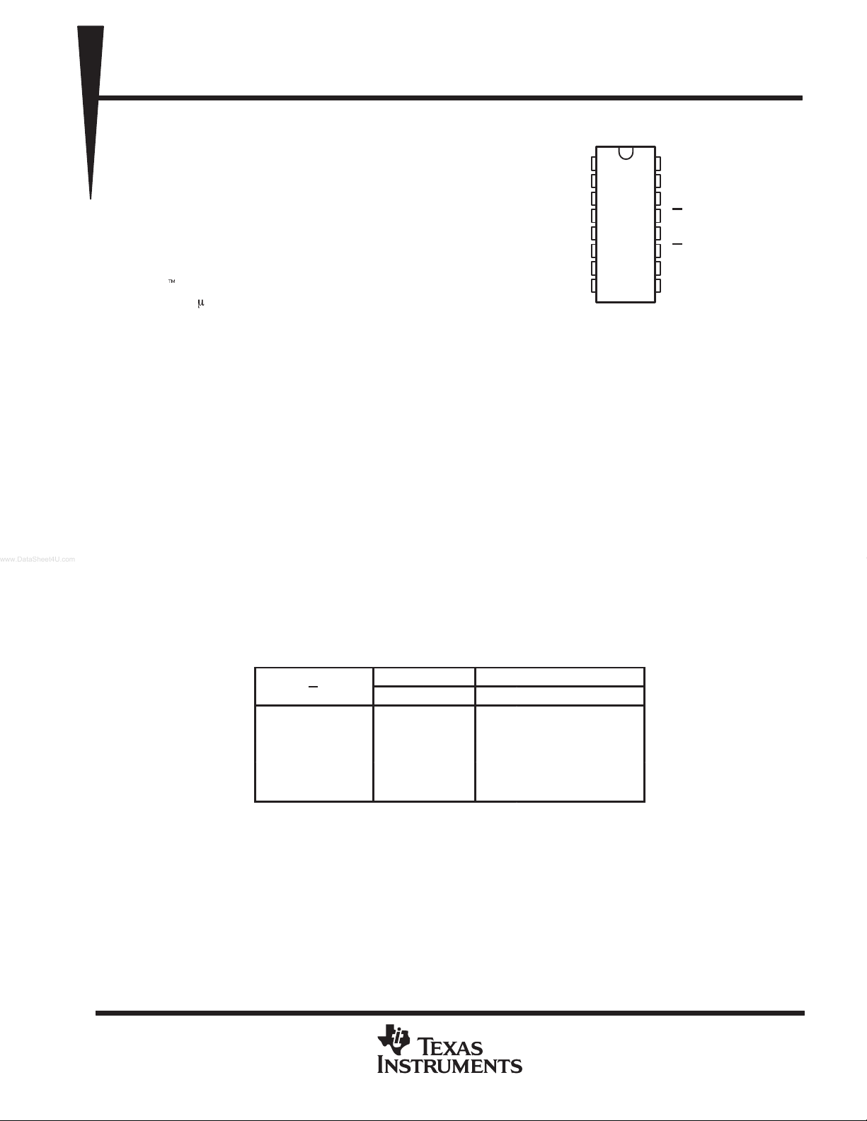
D OR N PACKAGE
(TOP VIEW)
Systems
• Incorporates Two Enable Inputs to Simplify
Cascading and/or Data Reception
• Flow-Through Architecture to Optimize
PCB Layout
• Center-Pin V
Minimize High-Speed Switching Noise
• EPIC
t
(Enhanced-Performance Implanted
and GND Configurations to
CC
1Y1
1Y2
1Y3
GND
2Y0
2Y1
2Y2
2Y3
1
2
3
4
5
6
7
8
15
14
13
12
11
10
1Y0
1A
1B
1G
V
CC
2G
2A
9
2B
16
CMOS) 1-mm Process
• 500-mA Typical Latch-Up Immunity
at 125°C
• Package Options Include Plastic Small
Outline Packages, and Standard Plastic
300-mil DIPs
description
The 74AC11239 circuit is designed to be used in high-performance memory-decoding or data- routing
applications requiring very short propagation delay times. In high-performance memory systems, this decoder
can be used to minimize the effects of system decoding. When employed with high-speed memories utilizing
a fast enable circuit, the delay times of this decoder and the enable time of the memory are usually less than
the typical access time of the memory . This means that the ef fective system delay introduced by the decoder
is negligible.
The 74AC1 1239 is comprised of two individual two-line to four-line decoders in a single package. The active-low
enable input can be used as a data line in demultiplexing applications. These decoders/demultiplexers feature
fully buffered inputs, each of which represents only one normalized load to its driving circuit.
The 74AC11239 is characterized for operation from – 40°C to 85°C.
FUNCTION TABLE
ENABLE INPUT
G
H X X L L L L
L L LHLLL
L H LLHLL
L L HLLHL
L H H L L L H
SELECT INPUTS OUTPUTS
A B Y0 Y1 Y2 Y3
EPIC is a trademark of Texas Instruments Incorporated.
PRODUCTION DATA information is current as of publication date.
Products conform to specifications per the terms of Texas Instruments
standard warranty. Production processing does not necessarily include
testing of all parameters.
POST OFFICE BOX 655303 • DALLAS, TEXAS 75265
POST OFFICE BOX 1443
Copyright 1993, Texas Instruments Incorporated
1
• HOUSTON, TEXAS 77251–1443
74AC11239
DUAL 2–LINE TO 4–LINE DECODER/DEMULTIPLEXER
SCAS072A – JULY 1989 – REVISED APRIL 1993
†
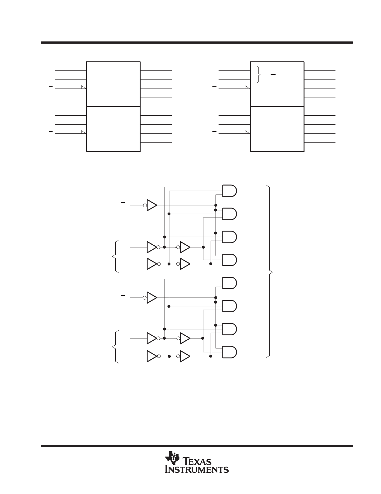
logic symbols
(alternatives)
15
1A
14
1B
13
1G
10
2A
9
2B
11
2G
†
These symbols are in accordance with ANSI/IEEE Std 91-1984 and IEC Publication 617-12.
0
1
EN
X/Y
16
0
1
2
3
1Y0
1
1Y1
2
1Y2
3
1Y3
5
2Y0
6
2Y1
7
2Y2
8
2Y3
1A
1B
1G
2A
2B
2G
15
14
13
10
9
11
logic diagram (positive logic)
1A
1B
13
15
14
Enable 1G
Select Inputs
16
DMUX
0
0
G
3
1
1Y0
1
1Y1
2
1Y2
3
1Y3
Data Outputs
5
2Y0
0
1
2
3
16
1Y0
1
1Y1
2
1Y2
3
1Y3
5
2Y0
6
2Y1
7
2Y2
8
2Y3
Enable 2G
Select
2A
2B
11
10
9
6
2Y1
7
2Y2
8
2Y3
2
POST OFFICE BOX 655303 • DALLAS, TEXAS 75265
POST OFFICE BOX 1443
• HOUSTON, TEXAS 77251–1443
74AC11239
DUAL 2–LINE TO 4–LINE DECODER/DEMULTIPLEXER
SCAS072A – JULY 1989 – REVISED APRIL 1993
absolute maximum ratings over operating free-air temperature range (unless otherwise noted)
Supply voltage range, V
CC
Input voltage range, VI (see Note 1) –0.5 V to VCC+ 0.5 V. . . . . . . . . . . . . . . . . . . . . . . . . . . . . . . . . . . . . . . . . . .
Output voltage range, VO (see Note 1) –0.5 V to VCC+ 0.5 V. . . . . . . . . . . . . . . . . . . . . . . . . . . . . . . . . . . . . . . .
Input clamp current, I
Output clamp current, I
Continuous output current, I
(V
< 0 or VI > VCC) ± 20 mA. . . . . . . . . . . . . . . . . . . . . . . . . . . . . . . . . . . . . . . . . . . . . . . . .
IK
I
(V
OK
< 0 or VO > VCC) ± 50 mA. . . . . . . . . . . . . . . . . . . . . . . . . . . . . . . . . . . . . . . . . . . .
O
(V
= 0 to VCC) ± 50 mA. . . . . . . . . . . . . . . . . . . . . . . . . . . . . . . . . . . . . . . . . . . . . .
O
O
Continuous current through VCC or GND ± 200 mA. . . . . . . . . . . . . . . . . . . . . . . . . . . . . . . . . . . . . . . . . . . . . . . . . .
Storage temperature range –65°C to 150°C. . . . . . . . . . . . . . . . . . . . . . . . . . . . . . . . . . . . . . . . . . . . . . . . . . . . . . . .
†
Stresses beyond those listed under “absolute maximum ratings” may cause permanent damage to the device. These are stress ratings only and
functional operation of the device at these or any other conditions beyond those indicated under “recommended operating conditions” is not
implied. Exposure to absolute-maximum-rated conditions for extended periods may affect device reliability.
NOTE 1: The input and output voltage ratings may be exceeded if the input and output current ratings are observed.
–0.5 V to 7 V. . . . . . . . . . . . . . . . . . . . . . . . . . . . . . . . . . . . . . . . . . . . . . . . . . . . . . . . . .
recommended operating conditions
MIN NOM MAX UNIT
V
V
V
V
V
I
I
Dt/D
T
Supply voltage 3 5 5.5 V
CC
VCC = 3 V 2.1
High-level input voltage
IH
Low-level input voltage
IL
Input voltage 0 V
I
Output voltage 0 V
O
High-level output current
OH
Low-level output current
OL
v Input transition rise or fall rate 0 10 ns/V
Operating free-air temperature –40 85 °C
A
VCC = 4.5 V
VCC = 5.5 V 3.85
VCC = 3 V 0.9
VCC = 4.5 V
VCC = 5.5 V 1.65
VCC = 3 V –4
VCC = 4.5 V
VCC = 5.5 V –24
VCC = 3 V 12
VCC = 4.5 V
VCC = 5.5 V 24
3.15
1.35
CC
CC
–24
24
V
V
V
V
mA
mA
†
POST OFFICE BOX 655303 • DALLAS, TEXAS 75265
POST OFFICE BOX 1443
• HOUSTON, TEXAS 77251–1443
3

74AC11239
PARAMETER
TEST CONDITIONS
V
MIN
MAX
UNIT
V
V
I
mA
V
V
I
24 mA
PARAMETER
MIN
MAX
UNIT
A or B
Y
ns
G
Y
ns
PARAMETER
MIN
MAX
UNIT
A or B
Y
ns
G
Y
ns
DUAL 2–LINE TO 4–LINE DECODER/DEMULTIPLEXER
SCAS072A – JULY 1989 – REVISED APRIL 1993
electrical characteristics over recommended operating free-air temperature range (unless
otherwise noted)
CC
3 V 2.9 2.9
IOH = – 50 mA
OH
OL
I
I
I
CC
C
i
†
Not more than one output should be tested at a time, and the duration of the test should not exceed 10 ms.
IOH = – 4 mA 3 V 2.58 2.48
= –24
OH
IOH = – 50 mA
IOH = – 75 mA
IOL = 50 mA
IOL = 12 mA 3 V 0.36 0.44
=
OL
IOL = 50 mA
IOL = 75 mA
VI = VCC or GND 5.5 V ± 0.1 ± 1
VI = VCC or GND, IO = 0 5.5 V 8 80
VI = VCC or GND 5 V 3.5 pF
{
{
{
{
4.5 V 4.4 4.4
5.5 V 5.4 5.4
4.5 V 3.94 3.8
5.5 V 4.94 4.8
5.5 V
5.5 V 3.85
3 V 0.1 0.1
4.5 V 0.1 0.1
5.5 V 0.1 0.1
4.5 V 0.36 0.44
5.5 V 0.36 0.44
5.5 V
5.5 V 1.65
TA = 25°C
MIN TYP MAX
m
A
m
A
switching characteristics over recommended operating free-air temperature range,
V
= 3.3 V ± 0.3 V (unless otherwise noted) (see Figure 1)
CC
TA = 25°C
MIN TYP MAX
1.5 6.2 8.5 1.5 9.5
1.5 5.6 8 1.5 9
1.5 5.4 7.1 1.5 7.9
1.5 5.7 7.3 1.5 8.1
t
PLH
t
PHL
t
PLH
t
PHL
FROM TO
(INPUT) (OUTPUT)
switching characteristics over recommended operating free-air temperature range,
V
= 5 V ± 0.5 V (unless otherwise noted) (see Figure 1)
CC
FROM TO
(INPUT) (OUTPUT)
t
PLH
t
PHL
t
PLH
t
PHL
operating characteristics, V
PARAMETER TEST CONDITIONS TYP UNIT
Cpd Power dissipation capacitance CL = 50 pF, f = 1 MHz 48 pF
= 5 V, TA = 25°C
CC
TA = 25°C
MIN TYP MAX
1.5 4 6.1 1.5 6.7
1.5 3.7 6.1 1.5 6.8
1.5 3.5 5.3 1.5 5.8
1.5 3.9 5.6 1.5 6.2
4
POST OFFICE BOX 655303 • DALLAS, TEXAS 75265
POST OFFICE BOX 1443
• HOUSTON, TEXAS 77251–1443

DUAL 2–LINE TO 4–LINE DECODER/DEMULTIPLEXER
SCAS072A – JULY 1989 – REVISED APRIL 1993
PARAMETER MEASUREMENT INFORMATION
From Output
Under Test
74AC11239
Input
(see Note B)
Output
NOTES: A.CL includes probe and jig capacitance.
B.Input pulses are supplied by generators having the following characteristics: PRR ≤ 10 MHz, ZO = 50 Ω, tr = 3 ns, tf = 3 ns.
C.The outputs are measured one at a time with one input transition per measurement.
Figure 1. Load Circuit and Voltage Waveforms
CL = 50 pF
(see Note A)
LOAD CIRCUIT
50% 50%
t
PLH
50%
PROPAGATION DELAY TIMES
500 Ω
t
50%
PHL
V
CC
0
V
OH
V
OL
POST OFFICE BOX 655303 • DALLAS, TEXAS 75265
POST OFFICE BOX 1443
• HOUSTON, TEXAS 77251–1443
5

PACKAGE OPTION ADDENDUM
www.ti.com
24-Jun-2005
PACKAGING INFORMATION
Orderable Device Status
(1)
Package
Type
Package
Drawing
Pins Package
Qty
Eco Plan
74AC11239D OBSOLETE SOIC D 16 TBD Call TI Call TI
74AC11239N OBSOLETE PDIP N 16 TBD Call TI Call TI
(1)
The marketing status values are defined as follows:
ACTIVE: Product device recommended for new designs.
LIFEBUY: TI has announced that the device will be discontinued, and a lifetime-buy period is in effect.
NRND: Not recommended for new designs. Device is in production to support existing customers, but TI does not recommend using this part in
a new design.
PREVIEW: Device has been announced but is not in production. Samples may or may not be available.
OBSOLETE: TI has discontinued the production of the device.
(2)
Eco Plan - The planned eco-friendly classification: Pb-Free (RoHS) or Green (RoHS & no Sb/Br) - please check
http://www.ti.com/productcontent for the latest availability information and additional product content details.
TBD: The Pb-Free/Green conversion plan has not been defined.
Pb-Free (RoHS): TI's terms "Lead-Free" or "Pb-Free" mean semiconductor products that are compatible with the current RoHS requirements
for all 6 substances, including the requirement that lead not exceed 0.1% by weight in homogeneous materials. Where designed to be soldered
at high temperatures, TI Pb-Free products are suitable for use in specified lead-free processes.
Green (RoHS & no Sb/Br): TI defines "Green" to mean Pb-Free (RoHS compatible), and free of Bromine (Br) and Antimony (Sb) based flame
retardants (Br or Sb do not exceed 0.1% by weight in homogeneous material)
(3)
MSL, Peak Temp. -- The Moisture Sensitivity Level rating according to the JEDEC industry standard classifications, and peak solder
temperature.
(2)
Lead/Ball Finish MSL Peak Temp
(3)
Important Information and Disclaimer:The information provided on this page represents TI's knowledge and belief as of the date that it is
provided. TI bases its knowledge and belief on information provided by third parties, and makes no representation or warranty as to the
accuracy of such information. Efforts are underway to better integrate information from third parties. TI has taken and continues to take
reasonable steps to provide representative and accurate information but may not have conducted destructive testing or chemical analysis on
incoming materials and chemicals. TI and TI suppliers consider certain information to be proprietary, and thus CAS numbers and other limited
information may not be available for release.
In no event shall TI's liability arising out of such information exceed the total purchase price of the TI part(s) at issue in this document sold by TI
to Customer on an annual basis.
Addendum-Page 1

IMPORTANT NOTICE
Texas Instruments Incorporated and its subsidiaries (TI) reserve the right to make corrections, modifications,
enhancements, improvements, and other changes to its products and services at any time and to discontinue
any product or service without notice. Customers should obtain the latest relevant information before placing
orders and should verify that such information is current and complete. All products are sold subject to TI’s terms
and conditions of sale supplied at the time of order acknowledgment.
TI warrants performance of its hardware products to the specifications applicable at the time of sale in
accordance with TI’s standard warranty. Testing and other quality control techniques are used to the extent TI
deems necessary to support this warranty . Except where mandated by government requirements, testing of all
parameters of each product is not necessarily performed.
TI assumes no liability for applications assistance or customer product design. Customers are responsible for
their products and applications using TI components. To minimize the risks associated with customer products
and applications, customers should provide adequate design and operating safeguards.
TI does not warrant or represent that any license, either express or implied, is granted under any TI patent right,
copyright, mask work right, or other TI intellectual property right relating to any combination, machine, or process
in which TI products or services are used. Information published by TI regarding third-party products or services
does not constitute a license from TI to use such products or services or a warranty or endorsement thereof.
Use of such information may require a license from a third party under the patents or other intellectual property
of the third party, or a license from TI under the patents or other intellectual property of TI.
Reproduction of information in TI data books or data sheets is permissible only if reproduction is without
alteration and is accompanied by all associated warranties, conditions, limitations, and notices. Reproduction
of this information with alteration is an unfair and deceptive business practice. TI is not responsible or liable for
such altered documentation.
Resale of TI products or services with statements different from or beyond the parameters stated by TI for that
product or service voids all express and any implied warranties for the associated TI product or service and
is an unfair and deceptive business practice. TI is not responsible or liable for any such statements.
Following are URLs where you can obtain information on other Texas Instruments products and application
solutions:
Products Applications
Amplifiers amplifier.ti.com Audio www.ti.com/audio
Data Converters dataconverter.ti.com Automotive www.ti.com/automotive
DSP dsp.ti.com Broadband www.ti.com/broadband
Interface interface.ti.com Digital Control www.ti.com/digitalcontrol
Logic logic.ti.com Military www.ti.com/military
Power Mgmt power.ti.com Optical Networking www.ti.com/opticalnetwork
Microcontrollers microcontroller.ti.com Security www.ti.com/security
Telephony www.ti.com/telephony
Video & Imaging www.ti.com/video
Wireless www.ti.com/wireless
Mailing Address: Texas Instruments
Post Office Box 655303 Dallas, Texas 75265
Copyright 2005, Texas Instruments Incorporated
 Loading...